Spread Aware™, Zero Del ay Buffer
W162
Cypress Semiconductor Corporation
• 3901 North First Street • San Jose • CA 95134 • 408-943-2600
July 31, 2000, rev. *B
Features
• Spread Aware™—designed to work with SSFTG
reference signals
• Two banks of four outputs, plus the fed back output
• Outputs may be three-stated
• Available in 16-pin SOIC or SSOP package
• Extra strength output drive available (-19 version)
• Internal feedback
Key Specifications
Operating Voltage: ............................................... 3.3V±10%
Operating Range: .................................15 < f
OUT
< 133 MHz
Cycle-to-Cycle Jitter: .................................... .............. 250 ps
Output to Output Skew: .......................... .................... 150 ps
Propagation Delay :..................................................... 150 ps
Table 1. Input Logic
SEL1 SEL0 QA0:3 QB0:3 PLL QFB
00Three-
State
Three-
State
Shutdown Active
01ActiveThree-
State
Active,
Utilized
Active
1 0 Active Active Shutdown,
Bypassed
Active
1 1 Active Active Active,
Utilized
Active
Spread Aware is a trademark of Cypress Semiconductor Corporation.
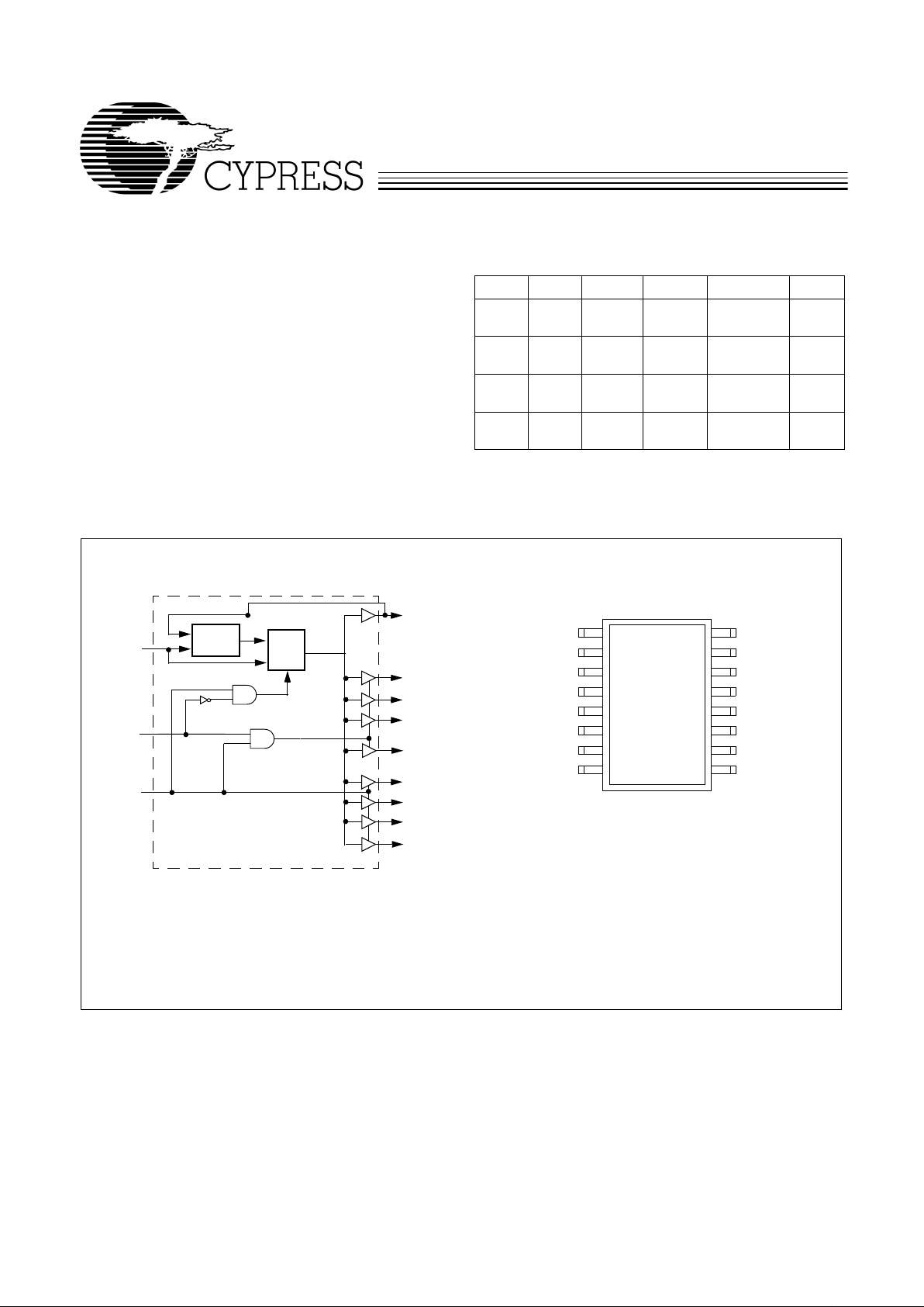
Block Diagram
Pin Configuration
PLL
REF
MUX
QA1
QA2
QA3
QB0
QB1
SEL0
QB2
QB3
SEL1
QFB
QA3
QA2
VDD
GND
QB3
QB2
SEL0
16
15
14
13
12
11
10
9
REF
QA0
QA1
VDD
GND
QB0
QB1
SEL1
1
2
3
4
5
6
7
8
QFB
QA0

W162
2
Overview
The W162 products are nine-output zero delay buffers. A
Phase-Lock ed Loop (PLL) is used to tak e a time-v arying signal
and provide eight copies of that same signal out.
Interna l feedback is used to m aximize the number of output
signals provid ed in the 16-p in package.
Spread Aware
Many systems b eing designed now util ize a technolog y ca lle d
Spread Spectrum F requency T iming Gener ation. Cypre ss has
been one of the pioneers of SSFTG development, and w e designed this product so as not to fil ter of f the S prea d Spe ctrum
feature of the Ref erence input, ass uming it exists . When a zero
delay buffer is not designed to pass the SS feature through,
the result is a significant amount of tracking skew which may
cause problems in systems requiring synchronization.
For more details on Spread Spectrum timing technology,
please see the Cyp ress App licat ion not e titled , “EMI Sup pression Techniques with Spread Spectrum Frequency Timing
Generator (SSFTG) ICs.”
Functional Description
Logic inputs pro v ide the us er th e ab ili ty to turn off one or both
banks of cloc k s wh en n o t in us e , a s d es crib ed i n Table 1. Disabling a bank of unused outputs will reduce jitter and power
consumption, and will als o reduce the amoun t of EMI generated by the W162.
These same inputs allo w the user to b ypass the PLL e ntirely if
so desired. When this is done, the device no longer acts as a
zero delay buffer, it simply reverts to a standard nine-output
clock driver.
Pin Definitions
Pin Name Pin No.
Pin
Type Pin Description
REF 1 I
Reference Input:
The output signals QA0:3 through QB0:3 will be synchro-
nized to this signal unless the device is programmed to bypass the PLL.
QFB 16 O
Feedback Output:
This signal is used as the feedback internally to esta b lish
the propagation delay of nearly 0.
QA0:3 2, 3, 14, 15 O
Outputs from Bank A:
The frequency of the signals provided by these pins
is equal to the signal connected to REF.
QB0:3 6, 7, 10, 11 O
Outputs from Bank B:
The frequency of the signals provided by these pins
is equal to the signal connected to REF.
VDD 4, 13 P
Power Conn ections:
Connect to 3.3V. Use ferrite beads to help reduc e noise
for optimal jitter performance.
GND 5, 12 P
Ground Connections:
Connect all grounds to the common system ground
plane.
SEL0:1 9, 8 I
Function Select Inputs:
Tie to V
DD
(HIGH, 1) or GND (LOW, 0) as desired
per Table 1.
 Loading...