Cypress W161H Datasheet

PRELIMINARY
133-MHz Spread Spectrum FTG f or Pentium® II Plat f orms
W161
Cypress Semiconductor Corporation
• 3901 North First Street • San Jose • CA 95134 • 408-943-2600
October 13, 1999, rev. **
Features
• Maximized EMI Suppression usi ng Cypress’s Spread
Spectrum Technology
• Three copies of CPU outputs at 100 or 133 MHz
• Three copies of 66-MHz output at 3.3V
• Ten copies of PCI clocks at 33 MHz, 3.3V
• T w o copies of 14.318-MHz refer ence output at 3.3V
• One copy of 48-MHz USB clock
• One copy of CPU- divide-b y-2 output as refer ence input
to Direct Rambus™ Clock Generator ( C ypress W134)
• Av ail able in 48-pin SSOP (300 mils)
Key Specific ati o n s
Supply Voltages:...................................... V
DDQ2
= 2.5V±5%
V
DDQ3
= 3.3V±5%
CPU, CPUdiv2 Output Jitter:............ .. .........................250 ps
CPU, CPUdiv2 Outp ut Skew:................... ................ ... 175 ps
IOAPIC, 3V66 Output Skew: . ...................................... 250 ps
PCI0:9 Output Skew:.......................... ................ ........ 500 ps
Duty Cycle: ...................................................................45/55
Spread Spectrum Modulation:..................................... –0.5%
CPU to 3V66 Output Offset:............ .0.0–1.5 ns (CPU leads)
3V66 to PCI Output Offset:.............. 1.5–3.0 ns (3V66 leads)
CPU to IOAPIC Output Offset:.........1.5–4.0 ns (CPU leads)
Pentium is a registered trademark of Intel Corporation. Direct Rambus is a trademark of Rambus, Inc.
T able 1. Pin Selectable Frequency
SEL133/100# SEL1 SEL0 Function
0 0 0 All outputs Three-State
001(Reserved)
0 1 0 Active 100-MHz, 48-MHz
PLL inactive
0 1 1 Active 100-MHz, 48-MHz
PLL active
1 0 0 Test Mode
101(Reserved)
1 1 0 Active 133-MHz, 48-MHz
PLL inactive
1 1 1 Active 133-MHz, 48-MHz
PLL active
Block Diagram
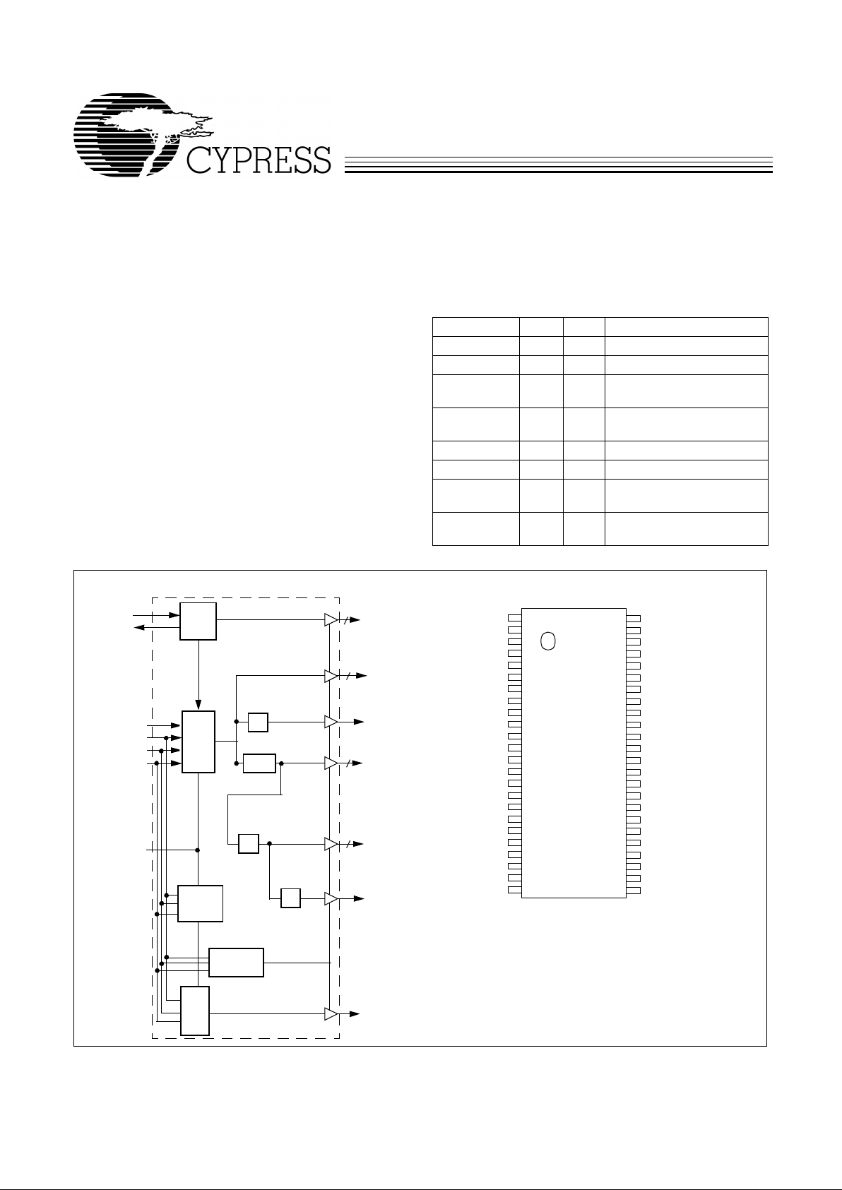
Pin Configuration
REF_[0:1]
CPU_[0:2]
CPUdiv2
3V66_[0:2]
XTAL
PLL 1
SPREAD#
X2
X1
PCI_[0:9]
IOAPIC
48MHz
PLL2
OSC
÷2
Power
Three-state
Logic
SEL0
SEL1
SEL133/100#
÷2/÷1.5
Down
Logic
÷2
÷2
2
3
3
9
PWRDWN#
REF0
REF1
VDDQ3
X1
X2
GND
PCI0
PCI1
VDDQ3
PCI2
PCI3
PCI4
PCI5
GND
PCI6
PCI7
VDDQ3
PCI8
PCI9
GND
3V66_0
3V66_1
3V66_2
VDDQ3
W161
GND
VDDQ2
IOAPIC
GND
VDDQ2
CPUdiv2
GND
VDDQ2
CPU2
GND
VDDQ2
CPU1
CPU0
GND
VDDQ3
GND
PWRDWN#*
SPREAD#*
SEL1*
SEL0*
VDDQ3
48MHz
GND
SEL133/100#
48
47
46
45
44
43
42
41
40
39
38
37
36
35
34
33
32
31
30
29
28
27
26
25
1
2
3
4
5
6
7
8
9
10
11
12
13
14
15
16
17
18
19
20
21
22
23
24
Note:
1. Internal 250-kΩ pull-up resistors present on inputs marked with *.
Design should not rely solely on internal pull-up resistor to set I/O
pins HIGH.
[1]

W161
PRELIMINARY
2
Overview
The W161, a motherboard clock synthesizer, provides 2.5V
CPU clock outputs for advanced CPU and a CPU-divide-by-2
refere nce frequency for Di rect Rambus
Clock Generat or (such
Cypress W134) int erfa ce. Fix ed output f requencie s are provi ded for other system functions.
CPU Frequency Selection
CPU frequency is selected with input pins 25, 29, and 30
(SEL133/100#, SEL0, and SEL1, re specti vel y). Ref er to Table
1 for detail s.
Output Buffer Configuration
Clock Output s
All clock outputs are designed to drive serial terminated clock
lines. The W161 outputs are CMOS-type, which provide
rail-to-rail output swi ng.
Crystal Oscillator
The W161 requires one input ref erence cl oc k to synt hesiz e all
output frequencies. The reference clock can be either an externally generated clock signal or the clock generated by the
internal crystal oscil lator. When using an e x ternal clo c k sig nal,
pin X1 is used as the clock in put and pin X2 is left open.
The internal crystal oscillator is used in conjunction with a
quartz crystal connected t o de vi ce pins X 1 and X2 . Th is f orms
a parallel resonant crystal oscillator circuit. The W161 incorporates the necessary feedback resistor and crystal load capacitors. Including typical stray circuit capacitance, the total
load presented to the crystal is approximately 18 pF. For optimum frequency accuracy without the addition of external capacitors, a parallel-resonant mode crystal s pecifying a load o f
18 pF sh ould be used . This will t ypically y ield referenc e frequency accuracies within ±100 ppm.
Pin Definitions
Pin Name
Pin
No.
Pin
T ype Pin Description
CPU0:2 36, 37, 40 O
CPU Clock Outputs 0 through 2:
CPU clock outputs. Their output volt age
swing is cont rolled by voltag e applied to VDDQ2.
PCI0:9 7, 8, 10, 11, 12,
13, 15, 16, 18,
19
O
PCI Clock Out puts 0 t hrough 9:
Output vo ltage s wing is control led by vo ltage
applied to VDDQ3.
CPUdiv2 43 O
CPU-Divide-By-2 Output:
This serves as a reference input signal for Direct
Rambus Clock G enerator (Cypress W134). The output voltage is determined
by VDDQ2.
3V66_0:2 21, 22, 23 O
66-MHz Clock Outputs 0 through 2:
Output volt age swing is controll ed by
voltage applied to VDDQ3.
IOAPIC 46 O
I/O APIC Clock Output:
Provides an out put synchronous to CPU clock. See
Ta ble 1 for their relation to other system clock outputs.
48 MHz 27 O
48-MHz Output:
Fixed clock output at 48 MHz.
SPREAD# 31 I
Spread Spectrum Enable:
This input enab les spread spectrum modulat ion
on the PLL1 generated f requency outputs of the W161. Modulation range is
–0.5%.
PWRDWN# 32 I
Power Down Control
REF0:1 1, 2 I
Fixed 14.318-MHz Output 0 and 1:
Output volt age swing is controll ed by
voltage applied to VDDQ3.
SEL0:1 29, 30 I
Mode Select Input 0 through 1:
3.3V LVTTL-compatible input for selecting
clock output mo des. As shown in Ta ble 1.
SEL133/100# 25 I
Frequency Selection Input:
3.3V LVTTL-compatible input that selec ts CPU
output frequen cy as shown in Table 1.
X1 4 I
Crystal Connection or Ext ernal Reference Freque ncy Input:
This pin has
dual functions. It can be used as an ex ternal 14.318-MHz crystal connection
or as an external reference frequency input.
X2 5 I
Crystal Connecti on:
An input connec tion f or an e xternal 14.3 18-MHz crystal.
If using an external reference , this pin must be left unconn ected.
VDDQ2 38, 41, 44, 47 P
Power Connection:
Connected to 2.5V power supply.
VDDQ3 3, 9, 17, 24, 28,
34
P
Power Connection:
Connected to 3.3V power supply.
GND 6, 14, 20, 26,
33, 35, 39, 42,
45, 48
G
Ground Connectio n:
Connect all ground pin s to th e common s ystem gr oun d
plane.

W161
PRELIMINARY
3
Spread Sp ectrum Feat u re
The device generates a clock that is frequency modulated in
order to increase the bandwidth that it occu pies. By increas ing
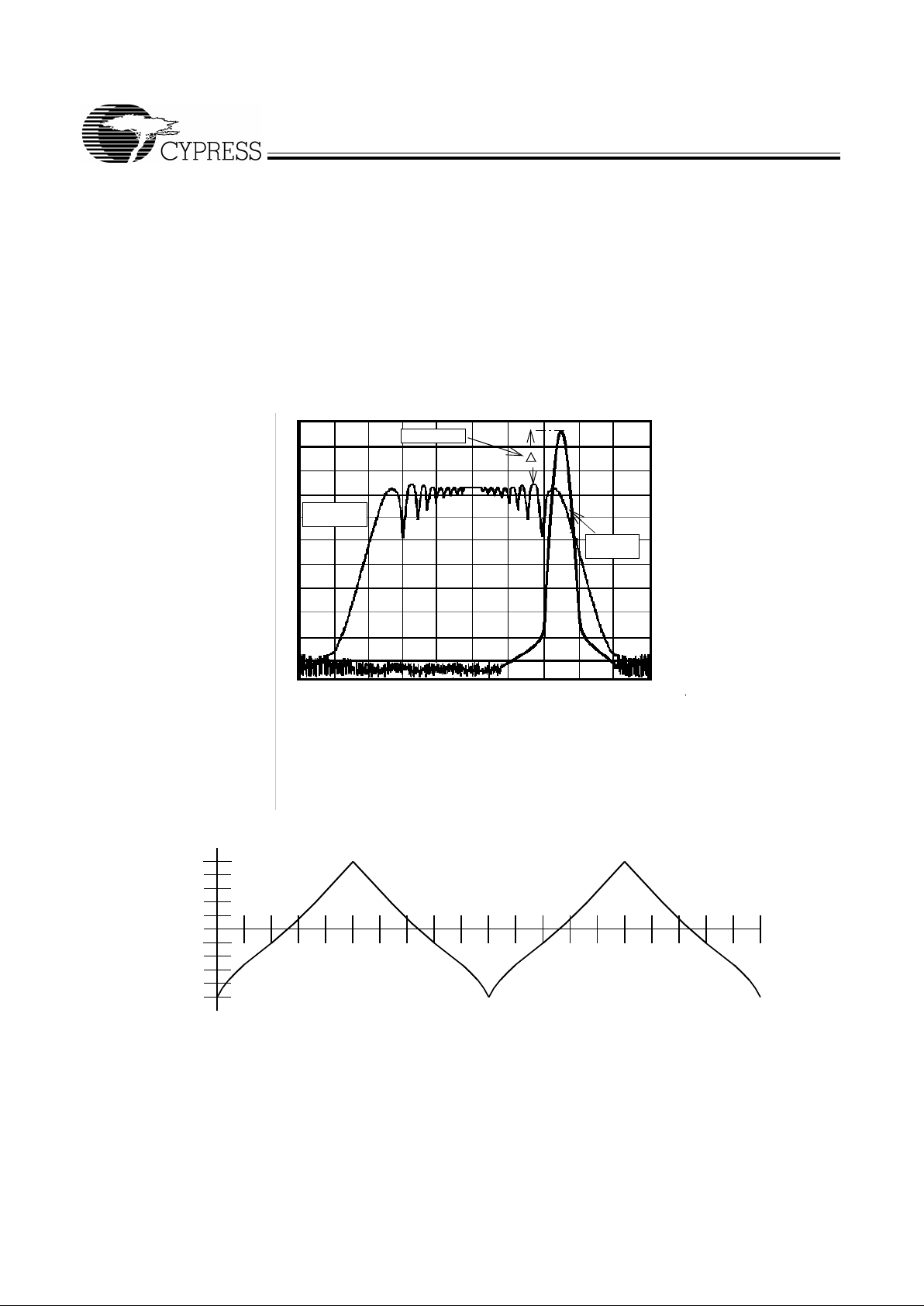
the bandwidth of the fundamental and its harmonics, the amplitudes of the radiated electromagnetic emissions are reduced. This effect is depicted in Figure 1.
As shown in Figure 1, a harmonic of a modulated cl ock has a
much low er amplitude th an that of an un modulated si gnal. The
reduction in amplitude is dependent on the harmonic number
and the frequency deviation or spread. The equation for the
reduction is
dB = 6.5 + 9*log
10
(P) + 9*log10(F)
Where P is the perce nta ge of de viati on and F is the frequen cy
in MHz where the reduction is measured.
The output clock is modulated with a waveform depicted in
Figure 2. This waveform, as discussed in “Spread Spect rum
Clock Generation f or the Reducti on of Radiated Emissio ns” by
Bush, Fessler, and Hardin produces the maximum reduction
in the amplitude of radiated electromagnetic emissions. The
deviati on selec ted for this chip i s –0.5% do wnspr ead. Fi gure 2
details the Cypress spr eading pat tern. Cypress does offer options with more spread and greater EMI reduction. Cont act
your local Sales representative for details on these devices .
Spread
Spectrum
Enabled
EMI Reduction
Spread
Spectrum
Non-
Figure 1. Typi cal Clock and SSFTG Comparison
100%
60%
20%
80%
40%
0%
–20%
–40%
–60%
–80%
–100%
10%
20%
30%
40%
50%
60%
70%
80%
90%
100%
10%
20%
30%
40%
50%
60%
70%
80%
90%
100%
Time
Frequency Shift
Figure 2. Typica l Modulation Profile
 Loading...