Spread Spectrum System Frequency Synthesizer
W158
Cypress Semiconductor Corporation
• 3901 North First Street • San Jose • CA 95134 • 408-943-2600
October 12, 1999, rev. **
Features
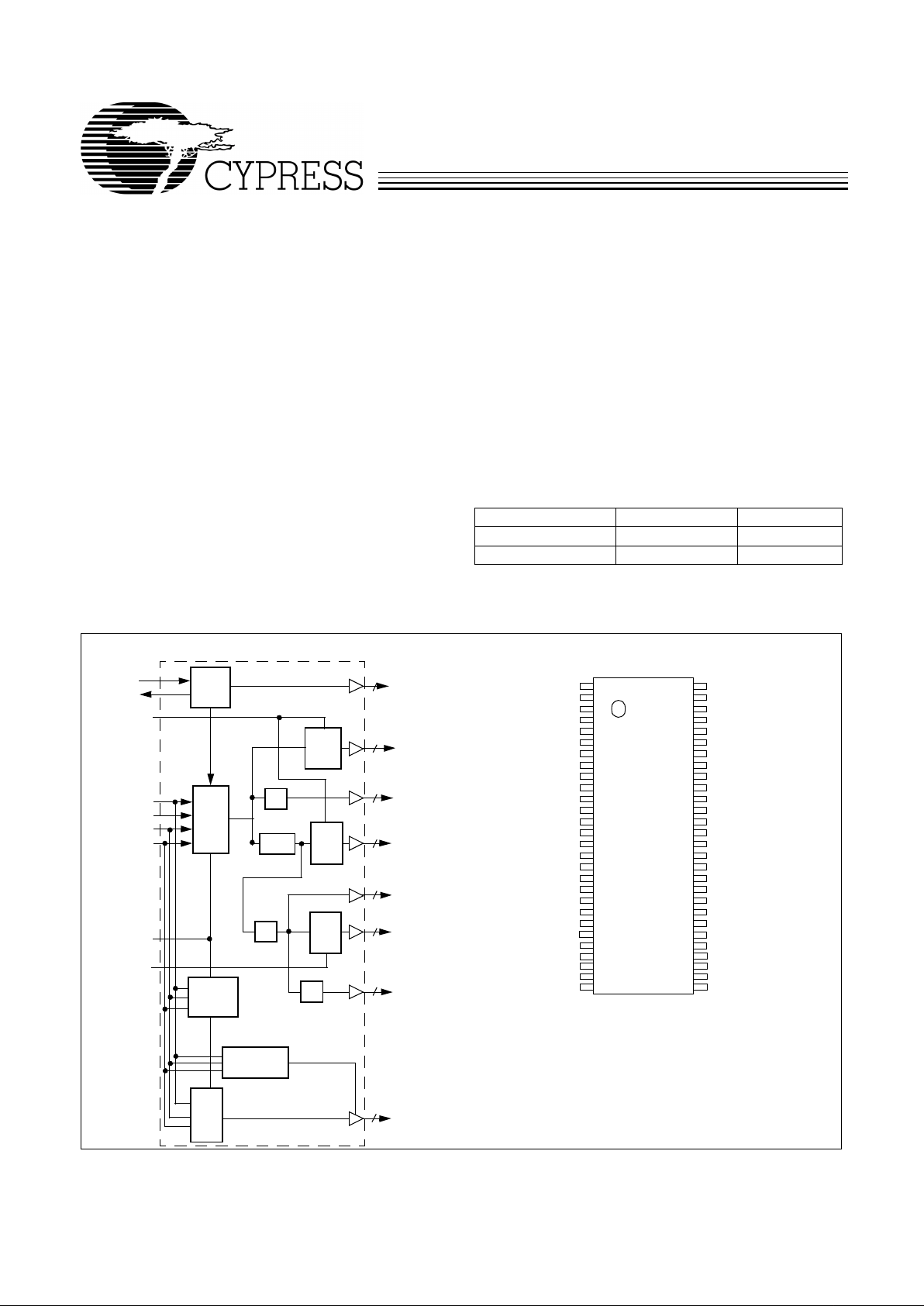
• Maximized EMI suppression usi ng Cypress’s spread
spectrum technology
• Int el® CK9 8 S p ecific ation co m p liant
• 0.5% downspread out puts deliver up to 10 dB lower EMI
• Four skew-controlled copies of CPU output
• Eight copies of PCI out put (synchronous w/CPU outp ut)
• Four copies of 66-MHz fix ed frequency 3.3V clock
• T wo copies of CPU/2 outputs for synchr onous memory
reference
• Three copies of 16. 67-MHz IO APIC clock , synchr onous
to CPU clock
• One copy of 48-MHz USB output
• Two copies of 14.31818-MHz reference clock
• Programmable to 133- or 100-MHz operation
• Power management control pins for cloc k stop and sh ut
down
• Available in 56-pin SSOP
Key Specific ati o n s
Supply Voltages:...................................... V
DDQ3
= 3.3V±5%
V
DDQ2
= 2.5V±5%
CPU Ou tp u t Ji tte r: . ... ......................................... .........15 0 p s
CPUdiv2, IOAPIC Output Jitter: ..................................250 ps
48 MHz, 3V66, PCI Output Jitter:................................500 ps
CPU0: 3, CP Ud iv 2 _ 0:1 O u tp u t Skew : ...... ... ............ ....175 ps
PCI_ F, PCI1:7 Out p u t Skew: ...... .. ............ ...................500 ps
3V66_0:3, IOAPIC0:2 Output Skew: ..................... ......250 ps
CPU to 3V66 Output Offset:.......... .0.0 to1.5 ns (CPU leads)
3V66 to PCI Output Offset:....... ... 1.5 to 3.0 ns (3V66 leads)
CPU to IOAPIC Output Offset: ......1.5 to 4.0 ns (CPU leads)
CPU to PCI Output Offset: ............ 1.5 to 4.0 ns (CPU leads)
Logic inputs, except SEL133/100#, have 250-kΩ pull-up
resistors
Intel is a registered trademark of Intel Corporation.
T able 1. Pin Selectable Frequency
[1]
SEL133/100# CPU0:3 (MHz) PCI
1 133 MHz 33.3 MHz
0 100 MHz 33.3 MHz
Note:
1. See
Table 2
for complete mode selection details.
Block Diagram
Pin Configuration
REF0:1
CPU0:3
CPUdiv2_0:1
3V66_0:3
XTAL
PLL 1
SPREAD#
X2
X1
PCI_F
PCI1:7
IOAPIC0:2
48MHz
PLL2
OSC
÷2
STOP
Logic
Power
Three-state
Logic
SEL0
SEL1
SEL133/100#
Clock
CPU_STOP#
÷2/÷1.5
STOP
Logic
Clock
Down
Logic
÷2
STOP
Logic
Clock
÷2
2
4
2
4
1
7
3
1
PCI_STOP#
PWRDWN#
GND
REF0
REF1
VDDQ3
X1
X2
GND
PCI_F
PCI1
VDDQ3
PCI2
PCI3
GND
PCI4
PCI5
VDDQ3
PCI6
PCI7
GND
GND
3V66_0
3V66_1
VDDQ3
GND
W158
VDDQ2
IOAPIC2
IOAPIC1
IOAPIC0
GND
VDDQ2
CPUdiv2_1
CPUdiv2_0
GND
VDDQ2
CPU3
CPU2
GND
VDDQ2
CPU1
CPU0
GND
VDDQ3
GND
PCI_STOP#
CPU_STOP#
PWRDWN#
SPREAD#
SEL1
56
55
54
53
52
51
50
49
48
47
46
45
44
43
42
41
40
39
38
37
36
35
34
33
1
2
3
4
5
6
7
8
9
10
11
12
13
14
15
16
17
18
19
20
21
22
23
24
25
26
27
28
32
31
30
29
3V66_2
3V66_3
VDDQ3
SEL133/100#
SEL0
VDDQ3
48MHz
GND

W158
2
Overview
The W158 is designed to provide the essential frequency
sources to work with advanced multiprocessing Intel architecture platforms. Split voltage supply signaling provides 2.5V
and 3.3V clock f requencies operating up to 133 MHz.
From a low-cost 14.31818-MHz reference crystal oscillator,
the W158 generates 2.5V clock outputs to sup port CPUs, core
logic chip set , and Direct RDRAM cloc k gener ators. It also provides skew-contr olled PCI and IOAPIC clock s synchronous t o
CPU clock, 48- MHz Universal Serial Bus (USB) clock, and replicates the 14.31818-MHz reference clock.
All CPU, PCI, and IOAPIC clocks can be synchronously modulated for spread spectrum operations. Cypress emp loys proprietary techniques that provide the maximum EMI reduction
while minimizing the clock skews that could reduce system
timing margins. Spread Spectrum modulation is enabled by
the active LOW control signal SPREAD#.
The W158 also includes po wer management contro l inputs. By
using these inputs, system logic can stop CPU and/or PCI
clocks or power down the entire device to conserve system
power.
Pin Definitions
Pin Name Pin No.
Pin
Type Pin Description
CPU0:3 41, 42, 45, 46 O
CPU Clock Outputs 0 through 3:
These four CPU clocks run at a frequency set by
SEL133/100#. Output voltage swing is set by the voltage applied to VDDQ2.
CPUdiv2_ 0:1 49, 50 O
Synchronous Memory Reference Clock Output 0 thro ugh 1:
Reference cl ock for Direct RDRAM clock gener at ors running a t 1/ 2 CPU cloc k fr equen cy. Out put v olt age s wing
is set by the voltage applied to VDDQ2.
PCI1:7 9, 11, 12, 14,
15, 17, 18
O
PCI Clock Outputs 1 through 7:
These seven PCI clock outputs run synchronously to
the CPU clock. Voltage swing is set by the po wer connection to VDDQ3. PCI1:7 outputs
are stopped when PCI _STOP# is held LOW.
PCI_F 8 O
PCI_F (PCI Free-running):
This PCI clock output runs synchr onous ly to the CPU clock.
V oltage swing i s set by the pow er connection to VDDQ3 . PCI_F is not affect ed by the stat e
of PCI_STOP#.
REF0:1 2, 3 O
14.318-MHz Reference Clock Output:
3.3V copies of the 14.318-MHz reference clock.
IOAPIC0:2 53, 54, 55 O
I/O APIC Clock Output:
Provides 16.67 -MHz fix ed fre quenc y. The out put vol tage s wi ng
is set by the power conn ection to VDDQ2.
48MHz 30 O
48-MHz Output:
Fixed 48-MHz USB output . Output voltage swing is controll ed by volt age
applied to VDDQ3.
3V66_0:3 21, 22, 25, 26 O
66-MHz Output 0 through 3:
Fixed 66-MHz outputs. Output volta ge swing is co ntrolled
by voltage applied to VDDQ3.
SEL0:1 32, 33 I
Mode Select Input 0 thr ough 1 :
3.3V LVT TL-compat ibl e i nput f or se lecti ng clo c k output
modes.
SEL133/100# 28 I
Frequency Selection Input:
3.3V LVTTL-compatible input that selects CPU output fr e-
quency as shown in Table 1 .
X1 5 I
Crystal Connection or External Reference Freque ncy Input:
Connect to either a
14.318-MHz crystal or an external reference signal.
X2 6 O
Crystal Connection:
An output connection for an external 14.318-MHz crystal. If using
an external reference, this pin must be left unconnected.
SPREAD# 34 I
Active LOW Spread Spectrum Enable:
3.3V LVTTL-compatible input tha t enables
spread spectrum mode when held LOW.
PWRDWN# 35 I
Active LOW Power Down Input:
3.3V LVTTL-compatible asynchronous input that re-
quests the devi ce to enter po wer-down mode.
CPU_STOP# 36 I
Active LOW CPU Cl ock Stop:
3.3V L VTTL- compatib le asyn chronous in put that s tops all
CPU and 3V66 clocks when held LOW. CPUdiv2 outputs are unaf fected by this input.
PCI_STOP# 37 I
Active LOW PCI Cloc k Stop:
3.3V LVTTL-compatibl e asyn chronous input th at stops all
PCI outputs exce pt PCI_F when held LO W.
VDDQ3 4, 10, 16, 23,
27, 31, 39
P
Power Connecti on:
Power supply for PCI output buffer s, 48-MHz USB output buffer ,
Reference out put buffers, 3V66 output buffer s, core logic, and PLL circuitry. Connect to
3.3V supply.
VDDQ2 43, 47, 51, 56 P
Power Connecti on:
Power supply for IOAPIC, CPU, and CPUdiv2 output buffers. Con-
nect to 2.5V supply.
GND 1, 7, 13, 19,
20, 24, 29, 38,
40, 44, 48, 52
G
Ground Connection:
Connect all ground pins to t he common system ground plane.

W158
3
Spread Sp ectrum Clockin g
The device generates a clock that is frequency modulated in
order to increase the bandwidth that it occu pies. By increas ing
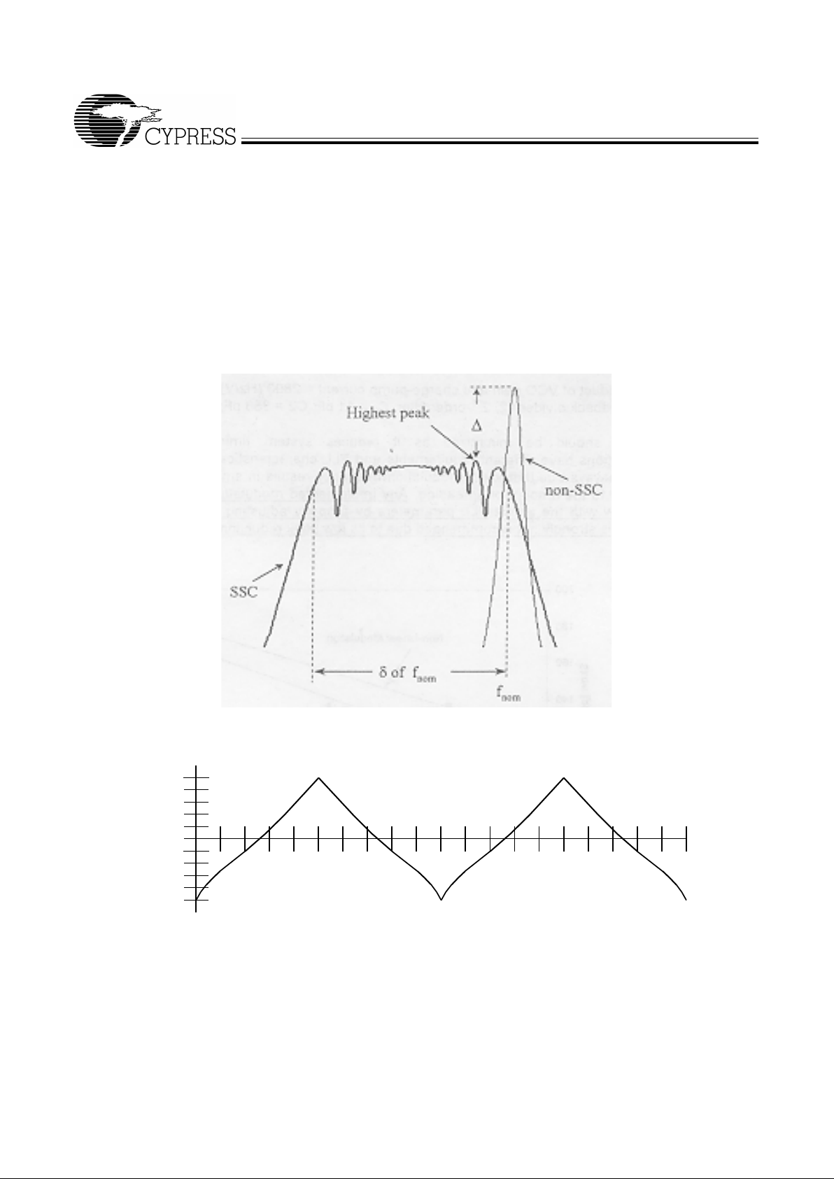
the bandwidth of the fundamental and its harmonics, the amplitudes of the radiated electromagnetic emissions are reduced. This effect is depicted in Figure 1.
As shown in Figure 1, a harmonic of a modulated clock has a
much low er amplitude th an that of an un modulated si gnal. The
reduction in amplitude is dependent on the harmonic number
and the frequency deviation or spread. The equation for t he
reduction is:
dB = 6.5 + 9*log
10
(P) + 9*log10(F)
Where P is the percentage of deviation and F is the frequency
in MHz where the reduction is measured.
The output clock is modulated with a waveform depicted in
Figure 2. This waveform , as discussed i n “Spread Spectrum
Clock Generation f or the Reducti on of Radiated Emissio ns” by
Bush, Fessler, and Hardin produces the maximum reduction
in the amplitude of radiated electromagnetic emissions. The
deviati on selec ted for this chip i s –0.5% do wnspr ead. Fi gure 2
details the Cypress spr eading pat tern. Cypress does offer options with more spread and greater EMI reduction. Contact
your local Sales representative for details on these devices.
Figure 1. Clock Harmonic with and without SSCG Modulation Frequency Domain Representation
100%
60%
20%
80%
40%
0%
–20%
–40%
–60%
–80%
–100%
10%
20%
30%
40%
50%
60%
70%
80%
90%
100%
10%
20%
30%
40%
50%
60%
70%
80%
90%
100%
Time
Frequency Shift
Figure 2. Modulation W aveform Profile

W158
4
Mode Selection Functions
The W158 supports the following operating modes controlled t hrough the SEL133/100#, SEL0, and SEL1 inputs.
Notes:
2. Provided for board level “bed of nails” testing.
3. 48-MHz PLL disabled to reduce component jitter.
4. Normal” mode of operation.
5. TCLK is a test clock over driven on the X1 input during test mode. TCLK mode is based on 133-MHz CPU select logic.
6. Required for DC output impedance verification.
7. Range of reference frequency is min.=14.316, nominal = 14.31818 MHz, max.=14.32 MHz.
8. Frequency accuracy of 48 MHz is +167 PPM to match USB default.
Table 2. Select Functi ons
SEL133/100# SEL1 SEL0 Function
0 0 0 All Outputs Three-State
00 1(Reserved)
0 1 0 Active 100-MHz, 48-MHz PLL Inactive
0 1 1 Active 100-MHz, 48-MHz PLL Active
1 0 0 Test Mode
10 1(Reserved)
1 1 0 Active 133-MHz, 48-MHz PLL Inactive
1 1 1 Active 133-MHz, 48-MHz PLL Active
Table 3. Truth Table
SEL
133/100# SEL1 SEL0 CPU CPUdiv2 3V66 PCI 48MHz REF IOAPIC Notes
0 0 0 HI-Z HI-Z HI-Z HI-Z HI-Z HI-Z HI-Z 2
0 0 1 n/a n/a n/a n/ a n/a n/a n/a
0 1 0 100 MHz 50 MHz 66 MHz 33 MHz HI-Z 14.318 MHz 16.67 MHz 3
0 1 1 100 MHz 50 MHz 66 MHz 33 MHz 48 MHz 14.318 MHz 16.67 MHz 4, 7, 8
1 0 0 TCLK/2 TCLK/4 TCLK/4 TCLK/8 TCLK/2 TCLK TCLK16 5, 6
1 0 1 n/a n/a n/a n/ a n/a n/a n/a
1 1 0 133 MHz 66 MHz 66 MHz 33 MHz HI-Z 14.318 MHz 16.67 MHz 3
1 1 1 133 MHz 66 MHz 66 MHz 33 MHz 48 MHz 14.318 MHz 16.67 MHz 4, 7, 8
Table 4. Maximum Supply Current
Condition
Max. 2.5V supply consumption
Max. discrete cap loads,
V
DDQ2
=2.625V
All static inputs=V
DDQ3
or GN D
Max. 3.3V supply consumption
Max. discrete cap loads,
V
DDQ3
=3.465V or GND
Powerdown Mode
(PWRDWN#=0)
100 µA 200 µA
Full Active 100 MH z
SEL133/100#=0
SEL1, 0=11
CPU_STOP#, PCI_ STOP#=1
75 mA 160 mA
Full Active 133 MH z
SEL133/100#=0
SEL1, 0=11
CPU_STOP#, PCI_ STOP#=1
90 mA 160 mA
 Loading...