

查询W152供应商
W152
Spread Aware™, Eight Output Zero Delay Buffer
Features
• Spread Aware ™—desi gned to work with SSFTG
reference signals
• T wo banks of four outputs each
• Configuration options to halve, double, or quadruple
the reference frequency refer to
Ta bl e 1
to determine
the specific option which meets your multiplication
needs
• Outputs may be three-stated
• Available in 16-pin SOIC package
• Extra strength output drive available (-11/-12 versions)
• Contact factory f or availabilit y information on 16-pin
TSSOP
Key Specific ati o n s
Operating Voltage: ............................................... 3.3V±10%
Operating Range: ... .................15 MHz < f
Cycle- to - C yc le Ji tte r: (Refer to
Figure 3
) ....... .............225 ps
OUTQA
< 140 MHz
Cycle-to-Cycle Jitter: Frequency Range
25 to140 MHz ........ ........................... .. ............. ....... 125 ps
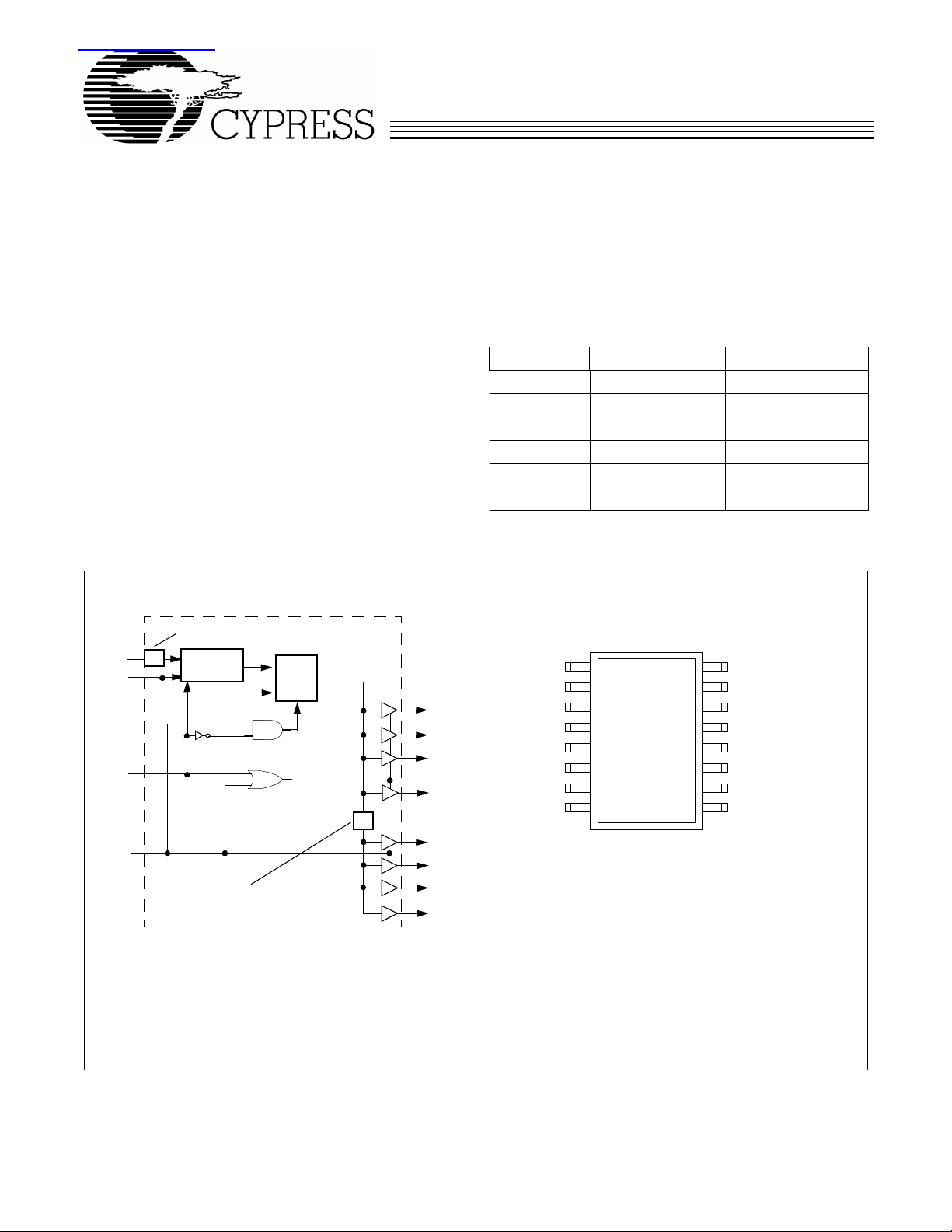
Block Diagram
(present on the -3 and -4 only)
FBIN
REF
SEL0
SEL1
÷2
PLL
(present on the -2, -12, and -3 only)
MUX
QA0
QA1
QA2
QA3
÷2
QB0
QB1
QB2
QB3
Output to Output Skew: Between Banks.....................215 ps
Output to Output Skew: Within Banks
(Refer to
Figure 4
) .................... ............ ............ ....... 1 0 0 p s
Total Timing Budget Impact:.......... ............. .. .. .............555 ps
Max. Phase Error Variation: ......................................±225 ps
Tracking S kew: ........... ............ ............ ............ ............±130 ps
T able 1. Configuration Options
Device Feedback Signal QA0:3 QB0:3
W152-1/11
W152-2/12
W152-2/12
[1]
QA0:3 or QB0:3 REFx1 REFx1
[2]
[2]
QA0:3 REFx1 REF/2
QB0:3 REFx2 REFx1
W152-3 QA0:3 REFx2 REFx1
W152-3 QB0:3 REFx4 REFx2
W152-4 QA0:3 or QB0:3 REFx2 REFx2
Notes:
1. W152-11 has stronger output drive than the W152-1.
2. W152-12 has stronger output drive than the W152-2.
Pin Configuration
REF
QA0
QA1
VDD
GND
QB0
QB1
SEL1
1
2
3
4
5
6
7
8
16
15
14
13
12
11
10
9
FBIN
QA3
QA2
VDD
GND
QB3
QB2
SEL0
Spread Aware is a trademark of Cypress Semiconductor Corporation.
Cypress Semiconductor Corporation
• 3901 North First Street • San Jose • CA 95134 • 408-943-2600
June 14, 2000, rev. *B
Pin Definitions
Pin Name Pin No.
REF 1 I
FBIN 16 I
QA0:3 2, 3, 14, 15 O
QB0:3 6, 7, 10, 11 O
VDD 4, 13 P
GND 5, 12 G
SEL0:1 9, 8 I
Pin
Type Pin Description
Reference Input:
this signal unless the device is program med to bypass the PLL.
Feedback Input:
fed by o ne of the ou tputs (QA0: 3 or QB 0:3) t o ensur e proper f unctio nality. If t he tr ace
between FBIN and the output pin being used for fe edback is equal in length to the
traces between the outputs and the signal destinations, then the signals rec eived at
the destinations will be synchronized to the REF signal input.
Outputs from Bank A:
mined by the f eedbac k signal connected to FBIN, and the sp ecific W152 op tion being
used. See Table 2.
Outputs from Bank B:
mined by the f eedbac k signal connected to FBIN, and the sp ecific W152 op tion being
used. See Table 2.
Power Connections:
optimal jitter performance.
Ground Connections:
Function Select Inputs:
T able 2.
The output signals QA0: 3 thr ough Q B 0:3 will be synchronized to
When programmed to zero delay buffer mode, this input must be
The frequency of the s ignals provided by these pins is deter-
The frequency of the s ignals provided by these pins is deter-
Connect to 3.3V. Use ferrite beads to help reduce noise for
Connect all grounds to the common system ground plane.
Tie to V
(HIGH, 1) or GND (LOW, 0) as desired per
DD
W152
Overview
The W152 products are eight-output zero delay buffers. A
Phase-Lock ed Loop (PLL) i s used to tak e a time- varying signal
and pro vide eight copies of that same signal out. The external
feedback to the PLL provides outputs in phase with the reference inputs.
Internal dividers exist in some options allowing the user to get
a simple multiple (/2, x2, x4) of the reference input, for details
see Table 1. Because the outputs are separated into two
banks, it is possi ble to provide some combin ation of these multiples at the sa me time.
Spread Aware
Many syst em s being designed no w utilize a tech nology called
Spread Spectrum F requency Timing Generation . Cypress has
been one of the pioneers of SSFTG develop me nt, and we designed this product so as not to filter off the Spread Spectrum
featur e of the Referen ce input, assuming i t ex ists. When a z ero
delay buffer is not designed to pass the SS feature through,
the result is a significant amount of tracking skew which may
cause problems in systems requiring synch ronization.
For more details on Spread Spectrum timing technology,
please see the Cypress application note titled, “EMI Suppression Techniques with Spread Spectrum Frequency Timing
Generator (SSFTG) ICs.”
Functional Description
Logic inputs pr ovide the user the abi li ty to turn off one or both
banks of clocks when not in use, as described in Table 2. Disabling a bank of unused outputs will reduce jitter and power
consumption, an d will als o reduce th e amoun t of EMI gener ated by the W152.
These same inputs al low t he user to by pass the PLL ent irely i f
so desired. When this is done, the device no longer acts as a
zero delay buffer, it simply reverts to a standard eight-output
clock driv er.
The W152 PLL enters an auto power- down mode when there
are no rising edges on the REF inpu t. In this mode, all output s
are three-stated and t he PLL is turned off.
T able 2. Input Logic
SEL1 SEL0 QA0:3 QB0:3 PLL
0 0 Three-State Three-State Shutdown
0 1 Active Three-State Active, Utilized
1 0 Active Active Shutdown,
Bypassed
1 1 Active Active Active, Utilized
2
W152
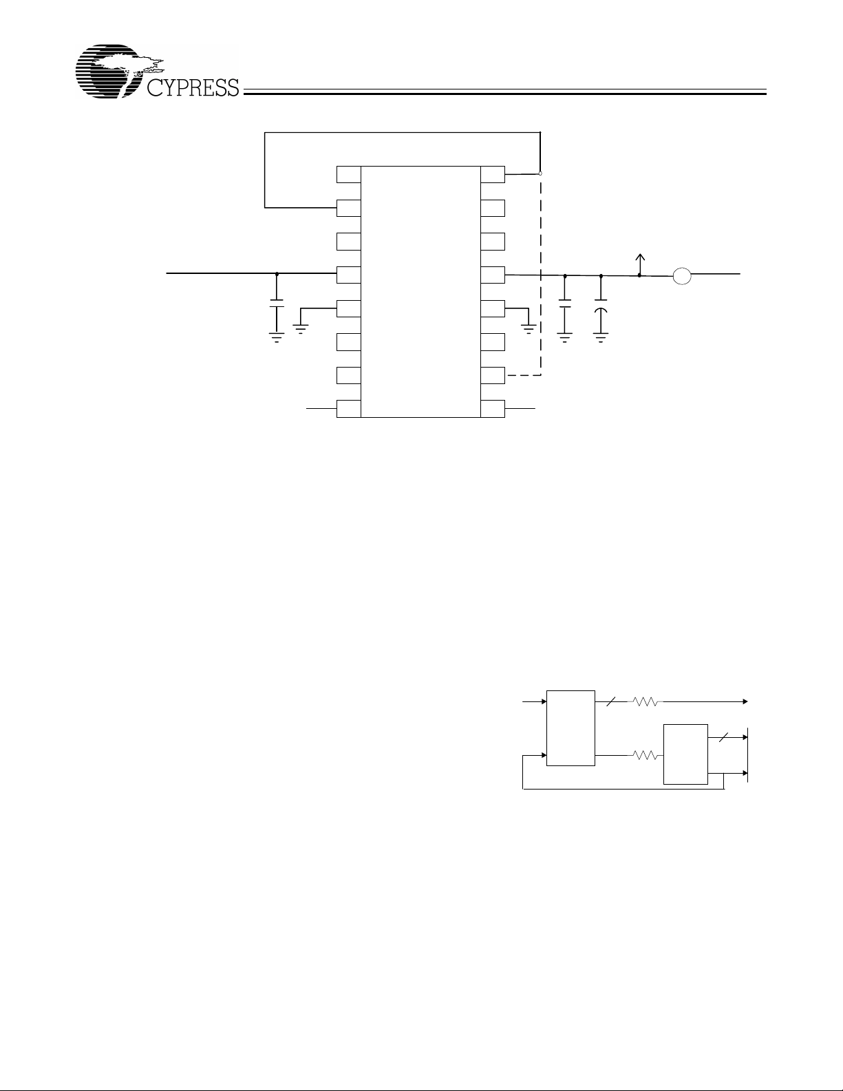
Figure 2. 6 Output Buffer in the Feedback Path
FB InRef In
QA3
QA2QA1
PowerPower
16
15
14
13
VDD
1
2
3
4
QA0
0.1 µF
Ground
5
QB0
6
QB1
7
SEL1 SEL0
VDD or GND (for desired operation mode)
Note:
3. Pin 16 needs to be connected to one of the outputs from either bank A or bank B, it should not be connected to both. Pins 2 and 10 are shown here as
examples. None of the outputs should be considered aas preferred for the feedback path.
8
Figure 1. Schematic
How to Implement Zero Delay
Typically, zero delay buffers (ZDBs) are used because a designer wants to provide multiple copies of a clock signal in
phase with each other . The whole c oncept be hind ZDBs is that
the signals at the destination chips are all going HIGH at the
same time as the input to the ZDB. In order to achieve this,
layou t must c ompensate f or tra ce length be tween the ZDB an d
the target devices. The method of compensation is described
below.
External feedbac k is the trait that allows f or thi s compensati on.
The PLL on the ZDB will cause the feedback signal to be in
phase with the reference signal. When laying out the board,
match the trace lengths between the output being used for
feedback and the FBIN input to the PLL.
If it is desirable to either add a little delay, or slightly precede
the input signal, this m ay also be affec ted by either making the
trace to the FBIN pin a little shorter or a little longer than the
traces to the devices being clocked.
Ground
12
QB3
11
QB2
10
9
[3]
some other dev ic e. Thi s impl ement ation can be appl ied t o an y
device (ASIC, mult iple output cloc k buffer /driver, etc.) which is
put into the feedback path.
Referring to Figure 2 , if the traces between the ASIC/buffer
and the destination of the clock signa l(s) (A) are equal in lengt h
to the trace between the buffer and the FBIN pin, the signals
at the destination(s) device will be driven HIGH at the same
time the Reference clock provided to the ZDB goes HIGH.
Synchronizing the other out puts of t he ZDB to the outputs f orm
the ASIC/Buff er is mor e comp le x ho we v er, as any propaga tion
delay in the ASIC/Buffer must be accounte d for.
Reference
Signal
Feedback
Input
See Note 3
Ferrite
0.1 µF
VDD
10 µF
Bead
VDD or GND (for desired operation mode)
Zero
Delay
Buffer
ASIC/
Buffer
3.3V
Supply
A
Inserti n g Other Devices in F eedback Path
Another nice feature available due to the external feedback is
the ability to synchronize signals up to the signal coming from
3
Absolute Maximum Ratings
W152
Stresses gre ater th an those li sted i n this tab le may cause permanent damage to the de vice. These represent a stress ratin g
only. Operation of the device at these or any other conditions
.
above those specified in the operating sections of this specification is not implied. Maximum conditions for extended periods may affect reliability.
Parameter Description Rating Unit
V
, V
DD
IN
T
STG
T
A
T
B
P
D
DC Electr i cal C h ar acteristics
Voltage on any pin with respect to GND –0.5 to +7 .0 V
Storage Temperature –65 to +150 °C
Operating Temperature 0 to +70 °C
Ambient Temperature under Bias –55 to +125 °C
Power Dissipation 0.5 W
:
=0°C to 70°C, VDD = 3.3V ±10%
T
A
Parameter Description Test Condition Min. Typ. Max. Unit
I
V
V
V
V
I
I
DD
IL
IH
OL
OH
IL
IH
Supply Current Unloaded, 100 MHz 40 mA
Input Low Voltage 0.8 V
Input High Voltage 2.0 V
Output Low Voltage IOL = 12 mA (-11, -12)
I
= 8 mA (-1, -2 , -3 , -4 )
OL
Output High Voltage IOH = 12 mA (-11, -12)
I
= 8 mA (-1, -2 , -3 , -4 )
OH
2.4 V
0.4 V
Input Low Current VIN = 0V 50 µA
Input High Current VIN = V
DD
50 µA
TA = 0°C to +70°C, VDD = 3.3V ±10%
AC Electrical Characteristics:
Parameter Description Test Condition Min. Typ. Max. Unit
f
IN
f
OUT
t
R
Input Frequency Note 3 15 140 MHz
Output Frequency 15-pF load
[8]
15 140 MHz
Output Rise Time (-1, -2, -3, -4) 0.8V to 0.8V, 15-pF load 2 2.5 ns
Output Rise Time (-11, -12) 0.8V to 0.8V, 15-pF load 1.5 ns
t
F
Output Fall Time (-1, -2, -3, -4) 2.0V to 0.8V, 15-pF load 2 2.5 ns
Output Rise Time (-11, -12) 2.0V to 0.8V, 20-pF load 1.5 ns
[5, 6]
[4]
[4]
4.5 ns
4.5 ns
350 ps
[7, 8]
[10]
45 50 55 %
215 ps
t
ICLKR
t
ICLKF
t
PD
t
SK
t
D
t
LOCK
t
JC
Notes:
3. Input frequency is limited by output frequency range and input to output frequency multiplication factor (which is determined by circuit configuration). See
Table 1
4. Longer input rise and fall time will degrade skew and jitter performance.
5. All AC specifications are measured with a 50Ω transmission line.
6. Skew is measured at V
7. Duty cycle is measured at V
8. For the higher drive -11 and -12, the load is 20 pF.
9. For frequencies above 25 MHz CY - CY = 125 ps.
10. Measured across all outputs. Maximum skew between outputs in the same bank is 100 ps.
Input Clock Rise Ti me
Input Clock Fall Time
FBIN to REF S kew
Output to Output Skew All outputs loaded equally
Duty Cycle 15-pF load
PLL Lock Time Power supply stable 1.0 ms
Jitter, Cycle-to-Cycle Note 9 225 ps
.
/2 on rising edges.
DD
/2.
DD
4

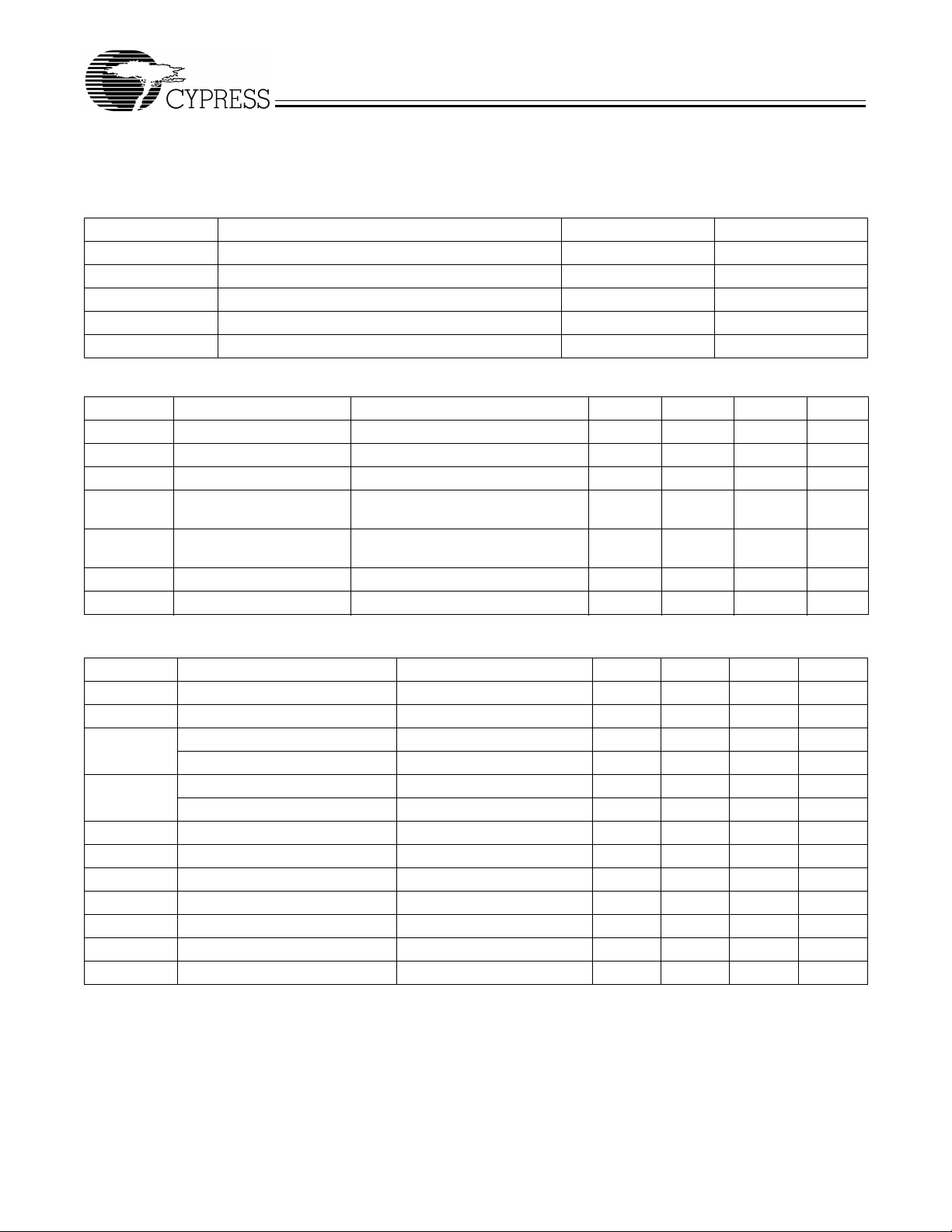
W152 -0 1 CYCLE - CYCLE JITTER @ 15 pF
1000
900
800
700
600
500
ps
400
300
200
100
0
0 20406080100120140160
FREQUENCY in MHz
07/21/99 W152-a1
Figure 3. Cycle to Cycle Jitt er at 15 pF
W152 - 01 PI N- PIN SKEW @ 15 pF
W152
300
200
100
ps
0
A1 A2 A3 A4 B1 B2 B3 B4
-100
-200
Ordering Information
Ordering Code Option
W152 -1, -11, -2 , -1 2 ,
-3, -4
Document #: 38-00786-*B
OUTPUT #
PIN A1 = RE F
O7/21/99 a3
Figure 4. Pin to Pin Skew at 15 pF
Package
Name Pack age Type
G
X
16-pin SOIC (150 mil)
16-pin TSSOP (4.4 mm)
5

Package Diagrams
W152
16-Pin Small Outline Integrated Circuit (SOIC, 150 mils)
6

W152
Package Diagrams
(continued)
16-Pin Thin Shrink Small Outline Package (TSSOP, 4.4 mm)
© Cypress Semiconductor Corporation, 2000. The information contained herein is subject to change without notice. Cypress Semiconductor Corporation assumes no responsibility for the use
of any circuitry other than circuitry embodied in a Cypress Semiconductor product. Nor does it con vey or imply any lice nse under patent or other rights. Cypress Semicondu ctor does not authorize
its products for use as critical components in life-support systems where a malfunction or failure may reasonably be expected to result in significant injury to the user. The inclusion of Cypress
Semiconductor products in life-support systems application implies that the manufacturer assumes all risk of such use and in doing so indemnifies Cypress Semiconductor against all charges.
 Loading...