Cypress W130H Datasheet

PRELIMINARY
Spread Spectrum Desktop/Notebook System Clock
W130
Cypress Semiconductor Corporation
• 3901 North First Street • San Jose • CA 95134 • 408-943-2600
October 27, 1999, rev. **
Features
• Maximized EMI suppression usi ng Cypress’s Spread
Spec t r u m techno logy
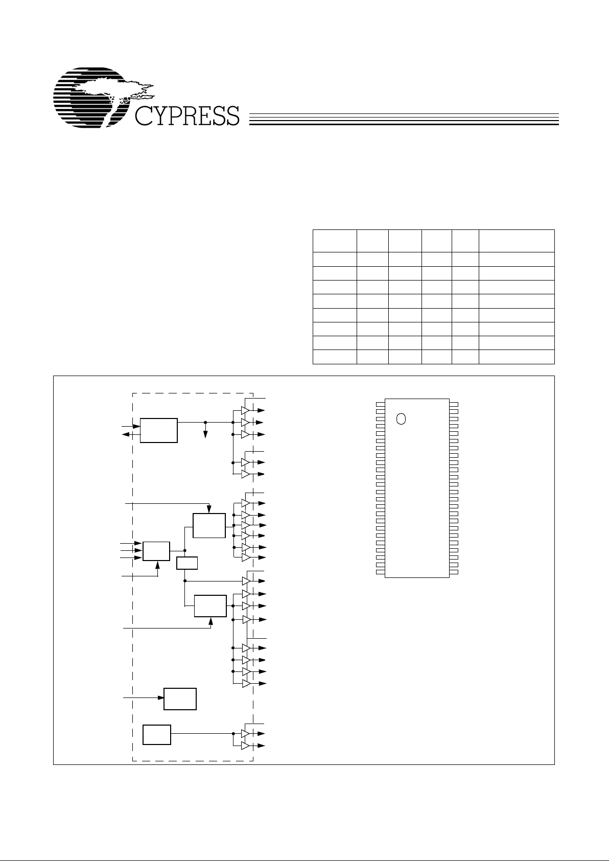
• Six copies of CPU Clock
• Eight copies of PCI Clock (synchronous w/CPU cloc k)
• T w o copies of 14.318-MHz IO APIC Clock
• T w o copies of 48-MHz USB Clock
• Three buffered copies of 14.318-MHz reference input
• Input is a 14.318-MHz XTAL or reference signal
• Selectable 100- M Hz or 66-MHz CPU Clocks
• Power man agem ent control input pins
• T est mode and output three-state capability
Key Specific ati o n s
Supply Voltages:.......................................V
DDQ3
= 3.3V±5%
V
DDQ2
= 2.5V±5%
CPU Clock Jitter: ...................... .. .. ............. .. .. .............200 ps
CPU0: 5 C lo ck Skew: .................... .. .................... .. ... .... 1 7 5 ps
PCI_ F, PCI1:7 Cl o ck Skew: ..... ... ......... ... .. .......... .. ... ....500 ps
CPU to PCI Clock Skew: ....... .. .....1.5 to 4.0 ns (CPU L e ad s )
Logic inpu ts have 250-kΩ pull-up resistors e xcept SEL100/66 #.
T able 1. Pin Selectable Frequency
SEL
100/66# SEL1 SEL0 CPU PCI SPREAD#=0
0 0 0 HI-Z HI-Z Don’t Ca re
0 0 1 66.6 33.3 ±0.9% Center
0 1 0 66.6 33.3 –1% Down
0 1 1 66.6 33.3 – 0.5% Down
1 0 0 X1/2 X1/6 Don’t Care
1 0 1 100 33.3 ±0.9% Center
1 1 0 100 33.3 –1% Down
1 1 1 100 33.3 –0.5% Down
Pin ConfigurationBlock Diagram
VDDQ3
REF0
VDDQ2
APIC0
CPU0
CPU1
CPU3
CPU5
PCI_F
XTAL
PLL Ref Freq
PLL 1
100/66#_SEL
X2
X1
REF1
VDDQ3
Stop
Clock
Control
Stop
Clock
Control
PCI1
PWR_DWN#
Power
Down
Control
PCI2
PCI3
PCI4
PCI5
48MHz
48MHz
PLL2
÷2/÷3
OSC
REF2
VDDQ2
PCI_STOP#
CPU_STOP#
PCI6
PCI7
VDDQ3
APIC1
SEL0
SEL1
VDDQ3
SPREAD#
CPU2
CPU4
Power
Down
Control
REF0
REF1
GND
X1
X2
GND
PCI_F
PCI1
VDDQ3
PCI2
PCI3
GND
PCI4
PCI5
VDDQ3
PCI6
PCI7
GND
VDDQ3
GND
VDDQ3
48MHz
48MHz
GND
VDDQ3
REF2
VDDQ2
APIC0
APIC1
VDDQ2
CPU0
CPU1
CPU2
CPU3
GND
VDDQ2
CPU4
CPU5
GND
VDDQ3
GND
PCI_STOP#
CPU_STOP#
PWRDWN#
SPREAD#
SEL0
SEL1
SEL100/66#
48
47
46
45
44
43
42
41
40
39
38
37
36
35
34
33
32
31
30
29
28
27
26
25
1
2
3
4
5
6
7
8
9
10
11
12
13
14
15
16
17
18
19
20
21
22
23
24

W130
PRELIMINARY
2
Pin Definitions
Pin Name
Pin
No.
Pin
Type Pin Description
CPU0:5 42, 41, 40,
39, 36, 35
O
CPU Clock Outputs 0 through 5:
These six CPU clock outputs are controlled b y
the CPU_STO P# contr ol pin . Output vol tage swing is cont roll ed by v oltag e appli ed
to VDDQ2.
PCI1:7 8, 10, 11, 13,
14, 16, 17
O
PCI Bus Clock Outputs 1 thr ough 7:
These sev en PCI clock outputs are cont rolled
by the PCI _STOP# con trol pin. Out put volt age swing is controlle d by v oltage applie d
to VDDQ3.
PCI_F 7 O
Fixed PCI Clock Output:
Unlike PCI 1:7 outputs , this output i s not cont rolled by the
PCI_STOP# control pin. Output voltage swing is controlled by voltage applied to
VDDQ3.
CPU_STOP# 30 I
CPU_STOP# Input :
When brought LO W, c lock output s CPU0: 5 are s topped LO W
after completing a full clock cycle (2–3 CPU clock latency). When brought HIGH,
clock out puts CPU0:5 start beginn ing with a full clock cyc le (2–3 CPU clock latency).
PCI_STOP# 31 I
PCI_STOP# I nput:
The PCI_STOP# input enables the PCI 1:7 out puts when HIGH
and causes them to remai n at l ogic 0 when LO W. The PCI_STOP signal i s latc hed
on the rising edge of PCI_F. Its effects take place on the next PCI_F clock cycle.
SPREAD# 28 I
SPREAD# Input:
When brough t LOW t his pin activ ates Spread Spectrum cloc king.
APIC0:1 45, 44 O
I/O APIC Clock Outputs:
Provides 14.31 8-MHz fi xed frequency. The output volt-
age swing is controlled by VDDQ2.
48MHz 22, 23 O
48-MHz Output s:
Fixed c lock output s at 48 MHz. Output vol tage swin g is controll ed
by volt age applied to VDDQ3.
REF0:2 1, 2, 47 O
Fixed 14.318-MHz Outp uts 0 through 2:
Used for various system applications.
Output voltage swing is contro ll ed by voltage appl ied to VDDQ3.
SEL100/66#
SEL1, SEL0
25, 26, 27 I
Frequency Selection Input:
Selects power-up default CPU clock frequency as
shown in Table 1 on page 1.
X1 4 I
Crystal Connection or Exte rnal Ref erence Freq uenc y Input:
Connect to either
a 14.318-MHz crystal or reference signal .
X2 5 I
Crystal Connection:
An input connection for an external 14.318-MHz crystal. If
using an external reference, this pin must be left unconnected.
PWR_DWN# 29 I
Power Down Control:
When this input is LOW , device goes into a lo w-power condition. All outputs are held LOW while in power-down. CPU and PCI clock outputs
are stopped LO W a fter co mpleti ng a ful l cl oc k cy cl e (2–3 CPU clock cyc le latency) .
When brought HIGH, CPU , SDRAM and PCI outputs start with a full cloc k cy cle at
full operating frequency (3 ms maximum lat ency).
VDDQ3 9, 15, 19, 21,
33, 48
P
Power Connection:
Power suppl y f or cor e logic , PLL circui try, PCI output buffers,
reference output buffers, and 48-MHz output buffers. Connected to 3.3V supply.
VDDQ2 37,43,46 P
Power Connection:
Powe r supply for APIC0:1and CPU0:5 output buffers. Con-
nected to 2.5V supply.
GND 3, 6, 12, 18,
20, 24, 32,
34, 38
G
Ground Connection:
Connect all ground pins to the common system ground
plane.

W130
PRELIMINARY
3
Spread Sp ectrum Clockin g
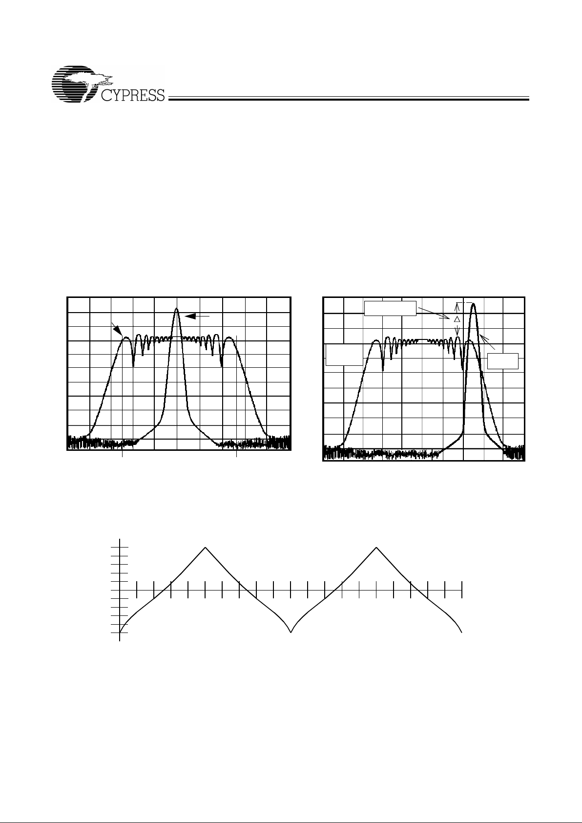
The device generates a clock that is frequency modulated in
order to increase the bandwidth that it occu pies. By increas ing
the bandwidth of the fundamental and its harmonics, the amplitudes of the radiated electromagnetic emissions are reduced. This effect is depicted in Figure 1.
As shown in Figure 1, a harmonic of a modulated clock has a
much low er amplitude th an that of an un modulated si gnal. The
reduction in amplitude is dependent on the harmonic number
and the frequency deviation or spread. The equation for the
reduction is:
dB = 6.5 + 9*log
10
(P) + 9*log10(F)
Where P is the perce nta ge of de viati on and F is the frequen cy
in MHz where the reduction is measured.
The output clock is modulated with a waveform depicted in
Figure 2. This waveform, as discussed in “Spread Spectrum
Clock Generation f or the Reducti on of Radiated Emissio ns” by
Bush, Fessler, and Hardin produces the maximum reduction
in the amplitude of radiated electromagnetic emissions. The
deviation selected for this chip is –0.5%, ±0.9 %, or –1.0% of
the selected frequency. Figure 2 detail s the Cypre ss spr eading
pattern. Cypress does offer options with more spread and
greater EMI r eduction. Cont act your local Sal es represe ntativ e
for details on these devices .
Spread Spectrum clocking is activated or deactivated by
SPREAD# input (pin 28).
Spread
Spectrum
Enabled
EMI Reduction
Spread
Spectrum
Non-
SSFTG Typical Clock
Frequency Span (MHz)
-SS%
+SS%
Amplitude (d B)
5dB/div
Figure 1. Clock Harmonic with and without SSCG Modulation Frequency Domain Representation
MAX (+0.5%)
MIN (–0.5%)
10%
20%
30%
40%
50%
60%
70%
80%
90%
100%
10%
20%
30%
40%
50%
60%
70%
80%
90%
100%
FREQUENCY
Figure 2. Typica l Modulation Profile
 Loading...