Cypress VIC068A-UMB, VIC068A-UM, VIC068A-NC, VIC068A-GMB, VIC068A-GI Datasheet
...
VMEbus Interface Controller
VIC068A
1VIC068A
Features
Complete VMEbus interface controller and arbiter
—58 internal registers provide c onfigur ation control
and status of VMEbus and local operations
—Drives arbitration, interrupt, address modifier utility,
strobe, address lines A07through A01 and data lines
D07 through D00 directly, and provides signals for
control logic to drive remaining address and data
line s
—Direct connection to 68xxx family and mappable to
non-68xxx processors
• Complete master/slave capability
—Supports read, write, write posting, and block trans-
fers
—Accommodates VMEbus timing requirements with
internal digital delay line (
—Programmable metastability delay
—Programmable data acquisition delays
—Provides timeout timers for local bus and VMEbus
transactions
• Interleaved block transfers over VMEbus
—Acts as DMA master on lo cal bus
—Programmable burst count, t ransfer length, and in-
terleaved period interval
— Supports local module-based DMA
• Arbitration support
—Supports single-level, priority and round robin arbi-
tration
—Supports fair request option as
requester
• Interrupt support
—Complete support for the VMEbus interrupts: inter-
rupter and interr upt handler
1
⁄2-clock granularity)
—Seven local interrupt lines
—8-level interrupt priority encode
—Total of 29 interrupts mapped through the VIC068A
• Miscellaneous features
—Refresh option for local DRAM
—Four broadcast location monitors
—Four module-specific location
monitor s
—Eight interprocessor communications registers
—PGA or QFP packages
—Compatible with IEEE Specification 1014, Rev. C
—Supports RMC operations
• See the
mation
VIC068A/V AC068A User’s Guide
for more infor-
Functional Description
The VMEbus interface controller (VIC068A) is a single chip
designed to minimize the cost and board area requirements
and to maximize performance of the VMEbus interface of a
VMEbus master/slave module. This can be implemented on
VIC068Aeither a 8-bit, 16-bit , or 32-bit VMEbus system. Th e
VIC068A performs all VMEbus system controller functions
plus many others, which simplify the development of
VIC068Aa VMEbus interface. The VIC068A utilizes patented
on-chip output buffers. These CMOS high-drive buffers provide direct connection to the address and data lines. In addition to these signals, the VIC068A connects directly to the arbitration, interrupt, address modifier, utility and strobe lines.
Signals are provided which control data direction and latch
functions needed for a 32-bit implementation.
The VIC068A was developed through the efforts of a consortium of board vendors, under the auspices of the VMEbus International Trade Association (VITA). The VIC068A thus insures compatibility between boards designed by different
manufacturers.
Cypress Semiconductor Corporation • 3901 North First Street • San Jose • CA 95134 • 408-943-2600
December 1990 – Revised April 1995

VIC068A
Pin Configurations
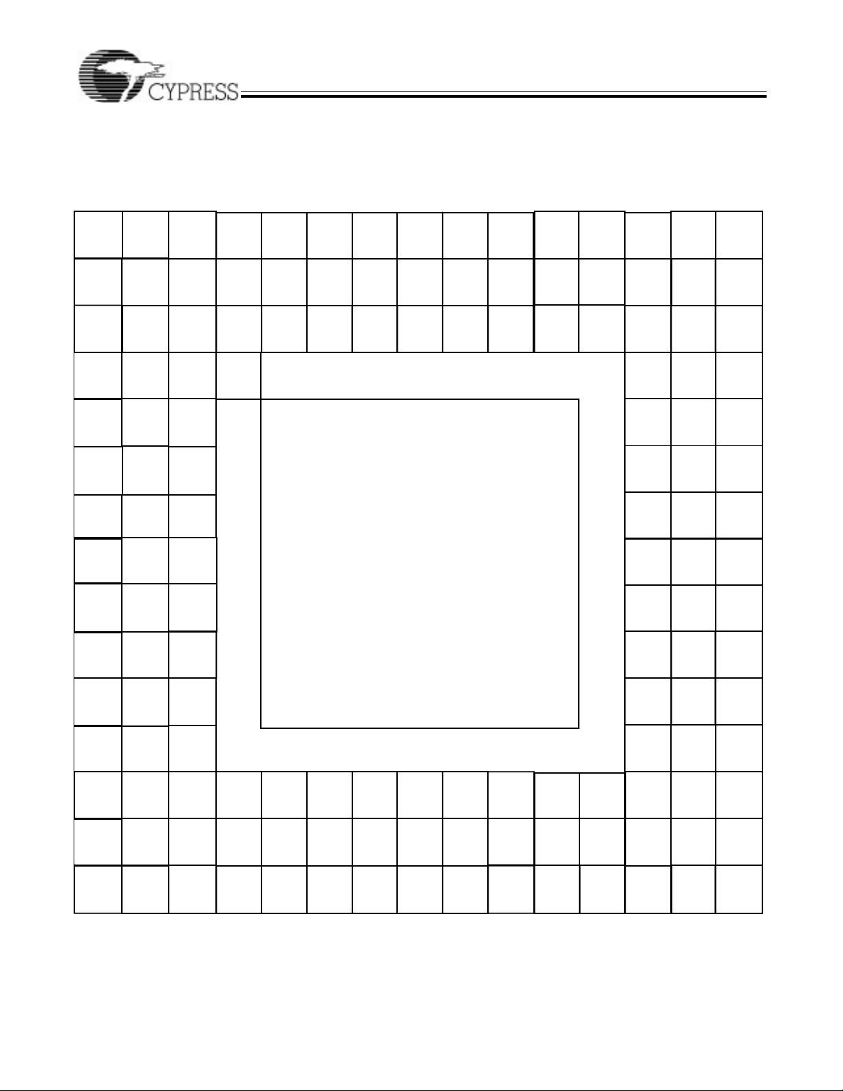
Pin Grid Array (PGA)
Bottom View
AB CDE FG HJ KL MN P R
GND
LD6
LD2
LD1
LA7
LA3
LA2
LA1
CS*
IPL2*
BLT*
LD5
LD3
LD0
LA5
LA4
LA0
DSACK1*
LIACKO*
IPL1*
DEDLK*
LD7
LD4
LA6
GND
VCC
DS*
LIRQ2*
VCC
IPL0*
LOCATOR
PIN
LIRQ5*
LIRQ1*
LAEN
ASIZ1
LIRQ4*
LIRQ3*
ASIZ0
LIRQ6*
LIRQ7*
SLSEL1*
ICFSEL*
GND
WORD*
MWB*
SLSEL0*
FIACK*
A01
GND
A02
A03
A06
A04
A05
IRQ1*
VCC
A07
IRQ2*
IRQ5*
SYSFAIL*
IACKIN*
GND
GND
VCC
GND
IRQ3*
IRQ6*
VCC
SYSRESET*
IACK*
AS*
AM2
LWORD*
IRQ4*
IRQ7*
ACFAIL*
IACKOUT*
DTACK*
AM0
AM1
AM3
AM4
PAS*
DSACK0*
HALT*
FC2
SIZ1
LBG*
LBERR*
R/W*
RMC*
SIZ0
IRESET*
ABEN*
RESET*
FC1
LBR*
SCON*
LADO
VCC
CLK64M
LEDI
LEDO
LADI
DDIR
UWDENIN*
GND
LWDENIN*
SWDEN*
VCC
DENO*
ISOBE*
GND
D06
D07
VCC
D03
D05
D00
D01
D04
BGOUT1*
GND
D02
BGIN2*
BGOUT0*
BGOUT3*
BERR*
BR2*
BBSY*
BGIN0*
BGIN3*
BGOUT2*
WRITE*
DS1*
BR1*
BR3*
BGIN1*
SYSCLK
AM5
DS0*
BR0*
GND
BCLR*
GND
VIC068A–1
2

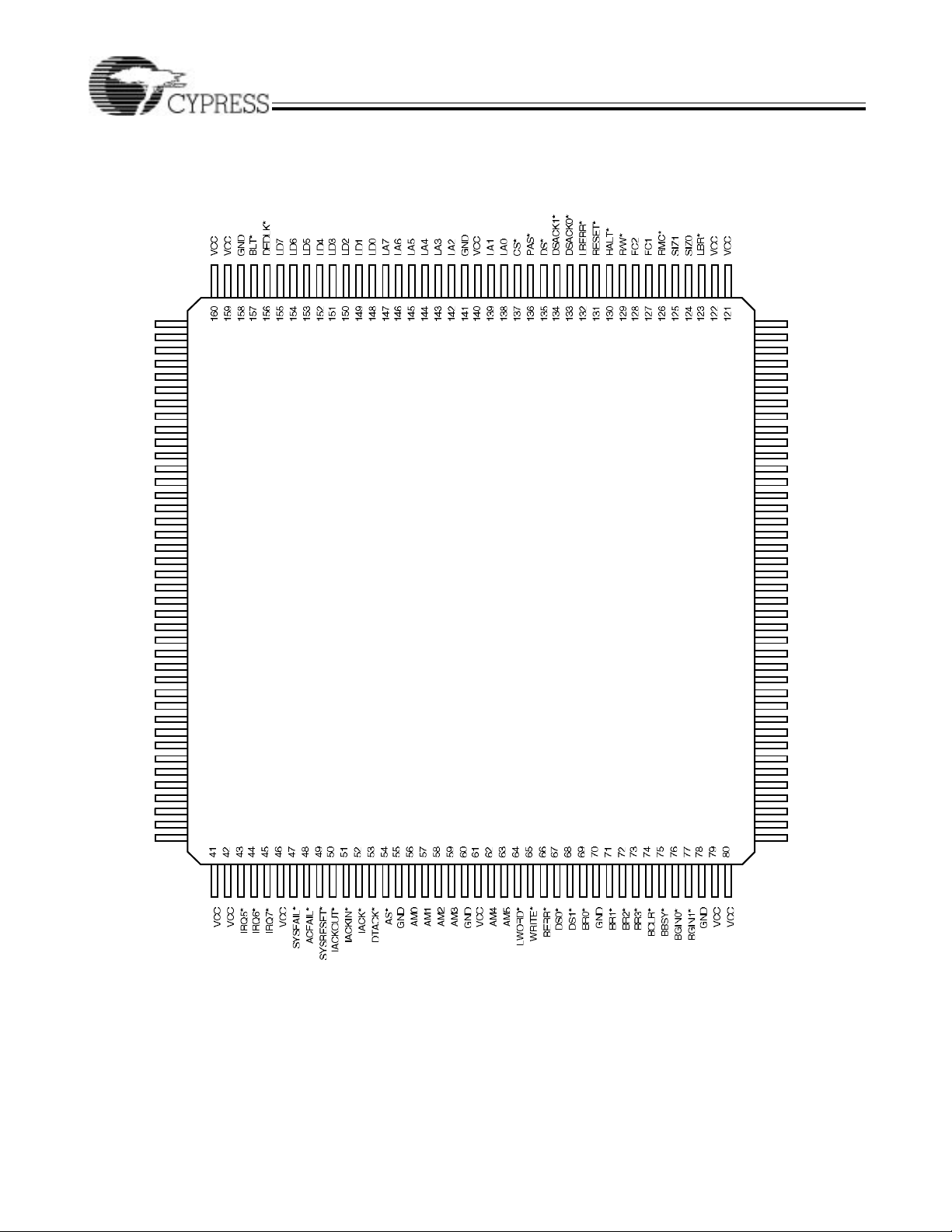
Pin Configurations (continued)
1GND 120 GND
2GND 119 GND
3IPL0* 118 LBG*
4IPL1* 117 IRESET*
5IPL2* 116 SCON*
6VCC 115 CLK64M
7LAEN 114 ABEN*
8LIAKO* 113 LADO
9LIRQ1* 112 LADI
10LIRQ2* 111 LEDI
11LIRQ3* 110 VCC
12LIRQ4* 109 LEDO
13LIRQ5* 108 DDIR
14LIRQ6* 107 UWDENIN*
15LIRQ7* 106 GND
16ASIZ1* 105 LWDENIN*
17ASIZ0* 104 DENO*
18ICFSEL* 103 SWDEN*
19SLSEL1* 102 ISOBE*
20GND 101 VCC
21SLSEL0* 100 GND
22WORD* 99 D07
23FCIACK* 98 D06
24MWB* 97 D05
25A1 96 D04
26GND 95 VCC
27A2 94 D03
28A3 93 D02
29A4 92 D01
30VCC 91 D00
31A5 90 BGOUT3*
32A6 89 GND
33A7 88 BGOUT2*
34VSS 87 BGOUT1*
35IRQ1* 86 BGOUT0*
36IRQ2* 85 SYSCLK
37IRQ3* 84 BGIN3*
38IRQ4* 83 BGIN2*
39GND 82 GND
40GND 81 GND
VIC068A
160-Pin QuadFlatpack (QFP)
Top View
VIC068A–2
3

Pin Configurations (continued)
VIC068A
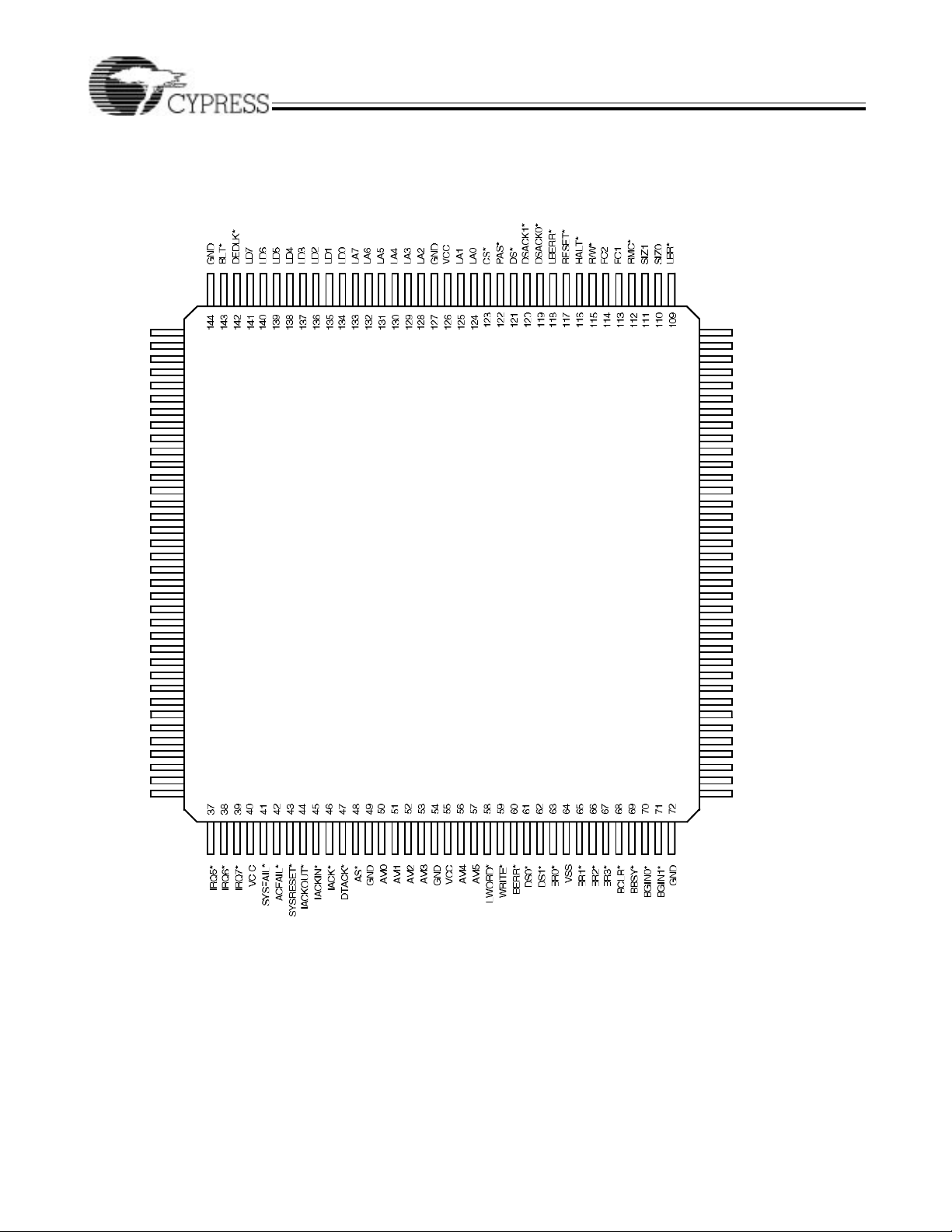
144-Pin Thin Quad Flatpack (TQFP)
TopView
IPL1* IRESET*
IPL2* SCON*
VCC CLK64M
LAEN ABEN*
LIAKO* LADO
LIRQ1* LADI
LIRQ2* LEDI
LIRQ3* VCC
LIRQ4* LEDO
LIRQ5*
LIRQ6*
LIRQ7*
ASIZ1*
ASIZ0*
ICFSEL*
SLSEL1*
GND
SLSEL0*
WORD*
FCIACK*
MWB*
A1
GND
A2
A3
A4
VCC
A5
A6
A7
GND
IRQ1*
IRQ2*
IRQ3*
IRQ4*
1
2
3
4
5
6
7
8
9
10
11
12
13
14
15
16
17
18
19
20
21
22
23
24
25
26
27
28
29
30
31
32
33
34
35
36
108
107
106
105
104
103
102
101
100
99
98
97
96
95
94
93
92
91
90
89
88
87
86
85
84
83
82
81
80
79
78
77
76
75
74
73
LBG*IPL0*
DDIR
UWDENIN*
GND
LWDENIN*
DENO*
SWDEN*
ISOBE*
VCC
GND
D07
D06
D05
D04
VCC
D03
D02
D01
D00
BGOUT3*
GND
BGOUT2*
BGOUT1*
BGOUT0*
SYSCLK
BGIN3*
BGIN2*
VIC068A–3
4

VIC068A on 68030 Board
512/256K X 36 DRAM 512/256K X 36 DRAM
VIC068A
68030
32
Latching Transceivers
LD0 –LD31
LA0 –LA31
Map Decoder
DRAM I/O
FCT
245
Address
Mux
EPROM
VMEbus
MWB*
WORD*
ASIZ1
ASIZ0
32
Latching Transceivers
4 JEDEC EPROMs
FCT
543
FCT
543
FCT
245
Parity Check
Logic
D24–D31
D16–D23
FCT
245
FCT
245
FCT
543
A31–A24 A23–16 A15–A08
FCT
543
FCT
543
ISOBE*
W1
Slave
Select
Decode
LD0 –LD7
LA0 –LA7
SCON*
SLSEL0*
SLSEL1*
ICFSEL
VIC068A
LIRQ1* - LIRQ7*LIACKO*
FCT
543
D08–D16
A1 – A 7
SYSCLK
D00 –D07
AM0 – AM5
AS*, DS0*, DS1*, DTACK*,
WRITE*, LWORD*, BERR*
BGiIN*, BGiOUT*, BRi*, BBSY*
IACK*, IACKIN*, IACKOUT*
IRQ1*, IRQ7*, ACFAIL*,
SYSFAIL*
STSRESET*
VIC068A–4
5
 Loading...