

Page 1

Please note that Cypress is an Infineon Technologies Company.
The document following this cover page is marked as “Cypress” document as this is the
company that originally developed the product. Please note that Infineon will continue
to oer the product to new and existing customers as part of the Infineon product
portfolio.
Continuity of document content
The fact that Infineon oers the following product as part of the Infineon product
portfolio does not lead to any changes to this document. Future revisions will occur
when appropriate, and any changes will be set out on the document history page.
Continuity of ordering part numbers
Infineon continues to support existing part numbers. Please continue to use the
ordering part numbers listed in the datasheet for ordering.
www.infineon.com
Page 2

Traveo II Starter Kit User Guide
Traveo II Starter Kit
User Guide
Document Number: 002-25314 Rev. *B
Cypress Semiconductor
An Infineon Technologies Company
198 Champion Court
San Jose, CA 95134-1709
www.cypress.com
www.infineon.com
Page 3

Copyrights
Copyrights
© Cypress Semiconductor Corporation, 2018-2020. This document is the property of Cypress Semiconductor Corporation and
its subsidiaries (“Cypress”). This document, including any software or firmware included or referenced in this document
(“Software”), is owned by Cypress under the intellectual property laws and treaties of the United States and other countries
worldwide. Cypress reserves all rights under such laws and treaties and does not, except as specifically stated in this paragraph,
grant any license under its patents, copyrights, trademarks, or other intellectual property rights. If the Software is not
accompanied by a license agreement and you do not otherwise have a written agreement with Cypress governing the use of the
Software, then Cypress hereby grants you a personal, non-exclusive, nontransferable license (without the right to sublicense)
(1) under its copyright rights in the Software (a) for Software provided in source code form, to modify and reproduce the Software
solely for use with Cypress hardware products, only internally within your organization, and (b) to distribute the Software in
binary code form externally to end users (either directly or indirectly through resellers and distributors), solely for use on Cypress
hardware product units, and (2) under those claims of Cypress's patents that are infringed by the Software (as provided by
Cypress, unmodified) to make, use, distribute, and import the Software solely for use with Cypress hardware products. Any other
use, reproduction, modification, translation, or compilation of the Software is prohibited.
TO THE EXTENT PERMITTED BY APPLICABLE LAW, CYPRESS MAKES NO WARRANTY OF ANY KIND, EXPRESS OR
IMPLIED, WITH REGARD TO THIS DOCUMENT OR ANY SOFTWARE OR ACCOMPANYING HARDWARE, INCLUDING,
BUT NOT LIMITED TO, THE IMPLIED WARRANTIES OF MERCHANTABILITY AND FITNESS FOR A PARTICULAR
PURPOSE. No computing device can be absolutely secure. Therefore, despite security measures implemented in Cypress
hardware or software products, Cypress shall have no liability arising out of any security breach, such as unauthorized access to
or use of a Cypress product. CYPRESS DOES NOT REPRESENT, WARRANT, OR GUARANTEE THAT CYPRESS
PRODUCTS, OR SYSTEMS CREATED USING CYPRESS PRODUCTS, WILL BE FREE FROM CORRUPTION, ATTACK,
VIRUSES, INTERFERENCE, HACKING, DATA LOSS OR THEFT, OR OTHER SECURITY INTRUSION (collectively, “Security
Breach”). Cypress disclaims any liability relating to any Security Breach, and you shall and hereby do release Cypress from any
claim, damage, or other liability arising from any Security Breach. In addition, the products described in these materials may
contain design defects or errors known as errata which may cause the product to deviate from published specifications. To the
extent permitted by applicable law, Cypress reserves the right to make changes to this document without further notice. Cypress
does not assume any liability arising out of the application or use of any product or circuit described in this document. Any
information provided in this document, including any sample design information or programming code, is provided only for
reference purposes. It is the responsibility of the user of this document to properly design, program, and test the functionality and
safety of any application made of this information and any resulting product. “High-Risk Device” means any device or system
whose failure could cause personal injury, death, or property damage. Examples of High-Risk Devices are weapons, nuclear
installations, surgical implants, and other medical devices. “Critical Component” means any component of a High-Risk Device
whose failure to perform can be reasonably expected to cause, directly or indirectly, the failure of the High-Risk Device, or to
affect its safety or effectiveness. Cypress is not liable, in whole or in part, and you shall and hereby do release Cypress from any
claim, damage, or other liability arising from any use of a Cypress product as a Critical Component in a High-Risk Device. You
shall indemnify and hold Cypress, its directors, officers, employees, agents, affiliates, distributors, and assigns harmless from
and against all claims, costs, damages, and expenses, arising out of any claim, including claims for product liability, personal
injury or death, or property damage arising from any use of a Cypress product as a Critical Component in a High-Risk Device.
Cypress products are not intended or authorized for use as a Critical Component in any High-Risk Device except to the limited
extent that (i) Cypress's published data sheet for the product explicitly states Cypress has qualified the product for use in a
specific High-Risk Device, or (ii) Cypress has given you advance written authorization to use the product as a Critical
Component in the specific High-Risk Device and you have signed a separate indemnification agreement.
Cypress, the Cypress logo, Spansion, the Spansion logo, and combinations thereof, WICED, PSoC, CapSense, EZ-USB, FRAM, and Traveo are trademarks or registered trademarks of Cypress in the United States and other countries. For a more
complete list of Cypress trademarks, visit cypress.com. Other names and brands may be claimed as property of their respective
owners.
Disclaimer of B. Schematics and Layouts
This material constitutes a reference design. CYPRESS MAKES NO WARRANTY OF ANY KIND, EXPRESS OR IMPLIED,
WITH REGARD TO THIS MATERIAL, INCLUDING, BUT NOT LIMITED TO. THE IMPLIED WARRANTIES OF
MERCHANTABILITY AND FITNESS FOR A PARTICULAR PURPOSE. Cypress reserves the right to make changes without
further notice to the materials described herein. Cypress does not assume any liability arising out of the application or use of any
product or circuit described herein. Cypress does not authorize its products for use as critical components in life-support
systems where a malfunction or failure may reasonably be expected to result in significant injury to the user. The inclusion of
Cypress products in a life-support systems application implies that the manufacturer assumes all risk of such use and in doing
so indemnifies Cypress against all changes.
Traveo II Starter Kit User Guide, Document Number: 002-25314 Rev. *B 2
Page 4
Preface
Using the Product Safely
This guide contains important information about using this product safely. Be sure to read this guide
before using the product and to follow the directions given to use the product correctly. In particular,
read “Product Caution” and perform a thorough safety check before using the product.
Store this guide in a safe location where it can easily be accessed at any time while you are using
the product.
Related Documents
Traveo™ II Automotive Body Controller Entry Family Architecture Technical Reference Manual
(TRM), 002-19314
Traveo™ II Automotive Body Controller Entry Registers Technical Reference Manual (TRM) for
CYT2B7, 002-19567
Traveo™ II Automotive Body Controller Entry Registers Technical Reference Manual (TRM) for
CYT2B9, 002-27181
CYT2B7 Datasheet 32-bit Arm
CYT2B9 Datasheet 32-bit Arm
®
Cortex®-M4F Microcontroller Traveo™ II Family, 002-18043
®
Cortex®-M4F Microcontroller Traveo™ II Family, 002-22825
Notice on This Document
All information included in this document is current as of the date it is issued. Such information is
subject to change without any prior notice.
Please confirm the latest relevant information with Cypress sales representatives.
Target Product
The following product is the target for this evaluation board.
Quantity Description Part No.
1 Traveo II Starter Kit CYTVII-B-E-1M-SK
Board Size
114 x 52 (mm).
Operating Temperature
0 to 40 °C.
Traveo II Starter Kit User Guide, Document Number: 002-25314 Rev. *B 3
Page 5

RoHS Compliance
European RoHS.
Traveo II Starter Kit User Guide, Document Number: 002-25314 Rev. *B 4
Page 6

Contents
1. Introduction 6
1.1 Precautions and Warnings...........................................................................................6
2. Overview 8
2.1 Functional Overview ....................................................................................................9
3. Operation Points and Locations 11
3.1 Power Supply.............................................................................................................11
3.2 Main Clock .................................................................................................................12
3.3 Switches ....................................................................................................................13
3.4 LEDs ..........................................................................................................................14
3.5 USB Interface Connector...........................................................................................15
3.6 CAN FD Interface Connector .....................................................................................16
3.7 Potentiometer ............................................................................................................17
3.8 Arduino Compatible Pin Headers ..............................................................................18
3.9 Debug Interface (Optional) ........................................................................................21
4. Known Limitations 22
4.1 Known Limitations......................................................................................................22
A. Connections and Settings 23
A.1 Traveo II Starter Kit Connections...............................................................................23
A.1.1 User LED........................................................................................................23
A.1.2 User SW.........................................................................................................23
A.1.3 RESET SW ....................................................................................................23
A.1.4 MODE SW......................................................................................................24
B. Schematics and Layouts 25
B.1 Schematics ................................................................................................................25
B.2 Layouts ......................................................................................................................36
Revision History 38
Traveo II Starter Kit User Guide, Document Number: 002-25314 Rev. *B 5
Page 7
1. Introduction
This guide provides directions for using the Traveo™ II Starter Kit, which is the evaluation
environment for Traveo II Body Entry devices of the Cypress Traveo II family 32-bit microcontroller.
Table 1-1. Contents - Traveo ll Starter Kit Board
Quantity Description Part No.
1 Traveo II Starter Kit Rev 3.0 CYTVII-B-E-1M-SK
Note: This user guide is meant for Rev 3.0 of the Traveo II Starter Kit.
1.1 Precautions and Warnings
The following precautions apply to the product described in this manual:
Warning
Electric shock,
Damage
Caution
Cuts, Damage
Damage
Indicates a potentially hazardous situation which could result in death or serious
injury and/or a fault in the user's system if the product is not used correctly.
Before performing any operation described in this manual, turn OFF all the power
supplies to the system.
Performing such an operation with the power ON may cause an electric shock or
device fault.
Once the product has been turned ON, do not touch any metal part of it.
Doing so may cause an electric shock or device fault.
Indicates a hazardous situation that may cause a minor or moderate injury, damages to this product or devices connected to it, or loss of software resources and
other properties such as data, if the device is not used appropriately.
Before moving the product, be sure to turn OFF all the power supplies and unplug
the cables. Watch your step when carrying the product. Do not use the product in
an unstable location such as a place exposed to strong vibration or with slopes.
Doing so may cause the product to fall, resulting in an injury or fault.
Do not place anything on the product or expose the product to physical shocks. Do
not carry the product after the power has been turned ON.
Doing so may cause a malfunction due to overloading or shock.
Since the product contains many electronic components, keep it away from direct
sunlight, high temperature, and high humidity to prevent condensation. Do not use
or store the product where it is exposed to much dust or a strong magnetic or electric field for an extended period.
Inappropriate operating or storage environments may cause a fault.
Traveo II Starter Kit User Guide, Document Number: 002-25314 Rev. *B 6
Page 8
Damage
Introduction
Use the product within the ranges given in the specifications.
Operation over the specified ranges may cause a fault.
To prevent electrostatic breakdown, do not let your finger or other object come in
contact with the metal parts of any connectors. Before handling the product, touch a
metal object (such as a door knob) to discharge any static electricity from your body.
When installing the sub board, align the key positions of main board connector and
sub board connector, and fix with the screw set before use. When removing,
remove all screws of screw set, and then remove the sub board vertically from the
main board. Otherwise, the product may be damaged, for example, the connector
section might be corrupted.
The product has no casing, so it is recommended that it be stored in the original
packaging. Transporting the product may cause a damage or fault. Therefore, keep
the packaging materials and use them when re-shipping the product.
Traveo II Starter Kit User Guide, Document Number: 002-25314 Rev. *B 7
Page 9
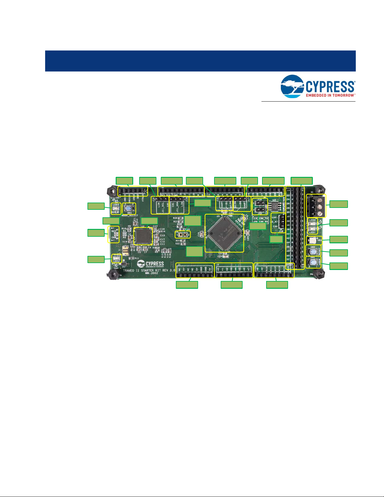
2. Overview
PSoc 5LP
Connector
Arduino compatible
pin header
Arduino compatible
pin header
Arduino compatible
pin header
J11_SCL
Selector
J11_SDA
Selector
J10_DO
Selector
J10_D1
Selector
Traveo II
CYT2B Series
MCU
CAN_TX/RX
Selector
J2_A7
Selector
U1 Current
Measurement
Jumper
Status LED
Mode Switch
USB micro
Connector
Power LED
PSoC 5LP
Arduino compatible
pin header
Arduino compatible
pin header
Arduino compatible
pin header
Arduino compatible
pin header
Potentiometer
Screw Terminal
for CANFD
User LEDs
RESET Switch
USER Switch
This evaluation board provides developers with the evaluation environment of the CYT2B75/95
MCU.
Figure 2-1. Traveo ll Starter Kit Board - Top View
Traveo II Starter Kit User Guide, Document Number: 002-25314 Rev. *B 8
Page 10
2.1 Functional Overview
Mode
Switch
Pull up
2.2 k
User
Switch
User LED
KitProg 3
(PSoC 5 LP)
CAN
Transceiver
USB
External
Prog/Debug
(No Load)
Status LED
External
Prog/Debug
(No Load)
Reset
Switch
I/O
Headers
(No Load)
Potentio
meter
CYT2B75/95
(Target Device)
I2C
UART
SWD
TX/RX
Power LED
Traveo II Starter Kit
This board can mount the CYT2B75/95 series of MCU. The location of the main function is shown in
Figure 2-2.
Figure 2-2. Traveo II Starter Kit Functional Overview
Overview
Traveo II Starter Kit User Guide, Document Number: 002-25314 Rev. *B 9
Page 11
Table 2-1. Traveo II Starter Kit Functions
Item Function Specification Remarks
CYT2B75XX
CYT2B95XX
Main clock 16 MHz
Surface mounted main crystal
oscillator and load capacitances
(10 pF)
CY8C5868LTI-LP039 U2: QFN 68-pin
Two User LEDs connected to
MCU
CAN FD channel
CAN0_1
Header 2.54-mm pitch 8 x 1 J1, J2, J7, J9, J10
Header 2.54-mm pitch 10 x 1 J11
Header 2.54-mm pitch 18 x 2 J13
MIPI-10/20 Arm JTAG
U1: QFP 100-pin (0.5-mm pitch)
X1: ABM10-16.000MHZ-D30-T3
LED1 Blue
LED4 Blue
J5: CAN0_1 (Screw Terminal)
U3: TJA1057GT
J3: FTSH-110-01-L-DV-K
Not mounted by default
Traveo II
Starter Kit
MCU
Oscillator
(optional)
PSoC 5LP KitProg3
Reset SW System reset switch SW2
User SW User switch connects to MCU SW1
Mode SW Mode switch connects to PSoC SW3
User LEDs
Power LED Power monitor LED LED2 Green
Status LED KitProg3 status LED LED3 Amber
USB connector USB micro connector J8: 10118194-0001LF
CAN FD interface
Potentiometer Potentiometer 10 kΩ VR1: 3313J-1-103E
Arduino compatible pin headers
Debug connector
(optional)
Overview
Traveo II Starter Kit User Guide, Document Number: 002-25314 Rev. *B 10
Page 12
3. Operation Points and Locations
R24, J4
USB micro
Bottom side
Resettable
Fuse
3.1 Power Supply
Power is supplied to this board from USB with a resettable fuse.
The current consumption can be measured at J4. J4 is not mounted by default, and instead R24 is
mounted. To measure current consumption, remove R24 and mount J4.
Figure 3-1. MCU Power Supply Jumper Locations
Traveo II Starter Kit User Guide, Document Number: 002-25314 Rev. *B 11
Page 13

3.2 Main Clock
X1
The main clock (X1) location and details are shown in Figure 3-2 and Tab l e 3 -1 .
X1 is a 16-MHz oscillator with load capacitance.
Figure 3-2. Main Clock Location
Operation Points and Locations
Table 3-1. Main Clock Oscillator
Part No. Model Number Remarks
X1 ABM10-16.000MHZ-D30-T3
ABRACON
Surface-mounted 16-MHz oscillator
Traveo II Starter Kit User Guide, Document Number: 002-25314 Rev. *B 12
Page 14

3.3 Switches
SW3
SW2
SW1
This board has various switches for performing certain operations. The location and details of these
switches are shown in Figure 3-3 and Table 3-2.
Figure 3-3. Switches Location
Operation Points and Locations
Table 3-2. Switches
Part No. Signal Name
SW1 User Switch: Connects to P7.0 of MCU
SW2 Reset Switch: System Reset
SW3 Mode Switch: Connects to P1[2] of PSoC 5LP
Traveo II Starter Kit User Guide, Document Number: 002-25314 Rev. *B 13
Page 15

3.4 LEDs
LED3
LED2
LED4
LED1
This board has various LEDs for condition indication. The location and details of these LEDs are
shown in Figure 3-4 and Table 3-3.
Figure 3-4. LED Location
Operation Points and Locations
Table 3-3. LEDs
Part No. Description
LED 1 User LED: Blue, Connects to P19.0 of DUT MCU
LED 2 Power LED: Green, Power monitor LED (VBUS)
LED 3 User LED: Amber, Connects to P1.4 of PSoC
LED 4 User LED: Blue, Connects to P12.2 of MCU
Traveo II Starter Kit User Guide, Document Number: 002-25314 Rev. *B 14
Page 16

3.5 USB Interface Connector
USB micro
Bottom side
This board has USB micro connector on the bottom side. SWD protocol is implemented on PSoC
over USB and is connected to MCU. The location and details of USB micro connector are shown in
Figure 3-5 and Tab le 3 -4 .
Figure 3-5. USB Interface Connector Location
Operation Points and Locations
Table 3-4. USB Interface Connector
Part No. Description Remarks
J8
USB micro connector
10118194-0001LF
FCI
This connector is mounted on the bottom side
Traveo II Starter Kit User Guide, Document Number: 002-25314 Rev. *B 15
Page 17

3.6 CAN FD Interface Connector
U3
J5
This board has a CAN FD interface. It is connected to a CAN FD channel of the DUT MCU.
The connector of CAN FD is 3-pin header. It is optional (not mounted by default). The CAN FD
interface connector location and details are shown in Figure 3-6 and Tab le 3- 5.
Figure 3-6. CAN FD Interface Connector Location
Operation Points and Locations
Table 3-5. CAN FD Interface
Part No. Description Remarks
U3
CAN FD Transceiver
TJA1057GT
J5 3-pin header (Screw terminal)
NXP
Connects to P0.2 and P0.3 (CAN0_1) of MCU
1: GND Common ground
2: CANL CAN0_1 bus signal LOW
3: CANH CAN0_1 bus signal HIGH
Traveo II Starter Kit User Guide, Document Number: 002-25314 Rev. *B 16
Page 18

3.7 Potentiometer
VR1
This board has a potentiometer. It is connected to an ADC channel of the MCU.
The potentiometer location and details are shown in Figure 3-7 and Tab le 3- 6.
Figure 3-7. Potentiometer Location
Operation Points and Locations
Table 3-6. Potentiometer
Part No. Description Remarks
VR1
Potentiometer 10 kΩ
3313J-1-103E
BOURNS
Connects to P6.0 (ADC[0]_0) of MCU
Traveo II Starter Kit User Guide, Document Number: 002-25314 Rev. *B 17
Page 19

3.8 Arduino Compatible Pin Headers
J1 J2
J9J10J11
J13
J7
This board has Arduino compatible pin headers to monitor MCU signals.
The location and details of I/O headers are shown in Figure 3-8, Ta bl e 3 -7 , Ta bl e 3 -8 , Ta b le 3 -9 ,
Ta bl e 3- 1 0, Tab le 3- 11 , Tab le 3- 12 and Tab le 3- 13 .
Figure 3-8. Arduino Compatible Pin Headers Location
Operation Points and Locations
Table 3-7. Arduino Compatible Pin Header 1 (J1)
Pin Signal
1NC
25V
3NC
4NC
55V
6GND
7GND
85V
Table 3-8. Arduino Compatible Pin Header 2 (J2)
Pin Signal
1 A0 (P7_5)
2 A1 (P7_4)
3 A2 (P7_3)
4 A3 (P6_5)
5 A4 (P6_4)
6 A5 (P13_2)
7 A6 (P12_1)
8A7
Traveo II Starter Kit User Guide, Document Number: 002-25314 Rev. *B 18
Page 20

Operation Points and Locations
Table 3-9. Arduino Compatible Pin Header 3 (J7)
Pin Signal
1 A8 (P7_0)
2 A9 (P18_6)
3 A10 (P18_7)
4NC
5NC
6NC
7NC
8NC
Table 3-10. Arduino Compatible Pin Header 4 (J9)
Pin Signal
1 14 (P18_1)
2 15 (P18_0)
3 16 (17_2)
4 17 (17_1)
5 18 (14_1)
6 19 (14_0)
7 20 (P0_3)
8 21 (P0_2)
Table 3-11. Arduino Compatible Pin Header 5 (J10)
Pin Signal
10
21
3 2 (P19_1)
4 3 (P19_2)
5 4 (P21_0)
6 5 (P21_1)
7 6 (P13_3)
8 7 (P13_5)
Traveo II Starter Kit User Guide, Document Number: 002-25314 Rev. *B 19
Page 21

Operation Points and Locations
Table 3-12. Arduino Compatible Pin Header 6 (J11)
Pin Signal
1SCL
2SDA
35V
4GND
5 13 (P22_2)
6 12 (P22_0)
7 11 (P22_1)
8 10 (P22_3)
9 9 (P23_3)
10 8 (P21_5)
Table 3-13. Arduino Compatible Pin Header 7 (J13)
Pin Signal Pin Signal
15V 25V
3 22 (P11_2) 4 23 (P11_1)
5 24 (P11_0) 6 25 (P8_2)
7 26 (P8_1) 8 27 (P18_2)
9 28 (P17_0) 10 29 (P14_3)
11 30 (P14_2) 12 31 (P13_7)
13 32 (P13_6) 14 33 (P13_4)
15 34 (P8_0) 16 35 (P3_0)
17 36 (P2_3) 18 37 (P12_4)
19 38 (P12_3) 20 39 (P12_2)
21 40 (P19_0) 22 41 (P3_1)
23 42 (P5_3) 24 43 (P2_0)
25 44 (P5_0) 26 45 (P5_1)
27 46 (P5_2) 28 47 (P18_3)
29 48 (P18_4) 30 49 (P18_5)
31 50 (P6_0) 32 51 (P6_1)
33 52 (P6_2) 34 53 (P6_3)
35 GND 36 GND
Traveo II Starter Kit User Guide, Document Number: 002-25314 Rev. *B 20
Page 22

3.9 Debug Interface (Optional)
This board has a MIPI-10/20 (Arm standard) connector as the debugging interface. This connector is
not mounted by default.
The debug connector location and details are shown in Tab le 3- 14 and Tab le 3 -1 5.
Operation Points and Locations
Table 3-14.
Part No. Description Remarks
J3
Debug Interface Connector (J3)
MIPI-20 connector
FTSH-110-01-L-DV-K
SAMTEC
Not mounted by default
(The foot pattern is available on the bottom side)
Table 3-15. MIPI-10/20 Connector
Pin Signal Pin Signal
1Power 2TMS
3Ground 4TCLK
5Ground 6TDO
7NC 8TDI
9 Ground 10 XRES
11 Ground 12 TRACE_CLOCK
13 Ground 14 TRACE_DATA_0
15 Ground 16 TRACE_DATA_1
17 Ground 18 TRACE_DATA_2
19 Ground 20 TRACE_DATA_3
Traveo II Starter Kit User Guide, Document Number: 002-25314 Rev. *B 21
Page 23

4. Known Limitations
4.1 Known Limitations
This section lists the known limitations of the Traveo ll Starter Kit.
Table 4-1. Limitation Information
No. Problem Description Workaround
1 CAN FD communication rate
limit
The external oscillator is
optional (Not mounted by
default) and the CAN FD
communication rate is 500
kbps at the maximum with
IMO
To evaluate communication rates
higher than that, install an external oscillator, or purchase an official evaluation board
Traveo II Starter Kit User Guide, Document Number: 002-25314 Rev. *B 22
Page 24

A. Connections and Settings
A.1 Traveo II Starter Kit Connections
A.1.1 User LED
The correspondence between the LEDs on the board and the CYT2B75XX/CYT2B95XX device pins
and the port pins as in Table A-1.
Table A-1. User LED
User
LED
USER LED LED1 77 P19.0
USER LED LED4 47 P12.2
A.1.2 User SW
The correspondence between the switch and the CYT2B75XX/CYT2B95XX device pin and the port
pin as in Tab le A -2 .
Table A-2. User Switch
User
SW
USER SW SW1 29 P7.0
A.1.3 RESET SW
The correspondence between the RESET SW and the CYT2B75XX/CYT2B95XX device pin and the
port pin as in Ta bl e A- 3.
Part Number
Part Number
CYT2B75XX/CYT2B95XX
Pin Pin Name
CYT2B75XX/CYT2B95XX
Pin Pin Name
Table A-3. RESET Switch
RESET
SW
RESET SW SW2 85 XRES
Traveo II Starter Kit User Guide, Document Number: 002-25314 Rev. *B 23
Part Number
Pin Pin Name
CYT2B75XX/CYT2B95XX
Page 25

A.1.4 MODE SW
The correspondence between the MODE SW and the PSoC 5LP pin number is given in Table A-4.
Table A-4. MODE Switch
Connections and Settings
RESET
SW
RESET SW SW3 13 P1[2]
Part Number
Pin Pin Name
PSoC 5LP
Traveo II Starter Kit User Guide, Document Number: 002-25314 Rev. *B 24
Page 26

B. Schematics and Layouts
B.1 Schematics
Traveo II Starter Kit User Guide, Document Number: 002-25314 Rev. *B 25
Page 27

BLOCK DIAGRAM
Traveo-II Starter Kit
USB
Mode
Switch
Pull up
2.2 K
User
Switch
User LEDs
TX/RX
Potentio
meter
I/O
Headers
(No Load)
External
Prog/Debug
(No Load)
External
Prog/Debug
(No Load)
Reset
Switch
Status LED
Power LED
KitProg3
(PSoC 5LP)
I
2
C
UART
SWD
CAN
Transceiver
CYT2B75/95
(Target Device)
Figure B-1. Schematic (1/10)
Schematics and Layouts
Traveo II Starter Kit User Guide, Document Number: 002-25314 Rev. *B 26
Page 28

Figure B-2. Schematic (2/10)
Note: Pull down to
disable HW flow control
Decoupling Capacitors
PSoC 5LP based KitProg3
Power LED
I2C Interface
USB Micro Connector
PSoC 5LP Power
PSoC 5LP Program/
Debug Connector
UART Interface
Mode Switch
KitProg3 Status LED
Target Power
Voltage Monitoring
SAR Bypass
Capacitor
Del-Sig Bypass
Capacitor
VBUS_R
UART_RX
UART_TX
UART_CTS
VBUS_F
KP_DM
KP_DP
P5LP_XRES
P5LP_SWDCLK
P5LP_SWDIO
P5LP1_2
P5LP_SIO_VREF
P5LP1_4_R
P5LP1_4
UART_CTS
KP_DM
KP_DP
VTARG_MEAS
USB_V_SENSE
P5LP_SIO_VREF
P5LP1_4
P3_2_C
USB_V_SENSE
VCCA_C
P5LP1_2
UART_RX
VTARG_MEAS
PO_4_C
KP_DP_R
KP_DM_R
UART_TX
P5LP_SWDIO
P5LP_SWDCLK
P5LP_XRES
P5LP_VCCD
P5LP_VCCD
P5LP_VDD
P5LP_VDD
P5LP_VDD
P5LP_VDD
P5LP_VCCD
P5LP_VDD
P5LP_VDD
VBUS
VTARG
VBUS
VTARG
P5LP_VDD
VBUS
VBUS
VTARG
VTARG
VTARG
VBUS
SG
DGND
DGND
DGND
DGND
DGND
DGND
DGND
DGND
DGND
DGND
DGND
DGND
DGND DGND
DGND
DGND
DGND
DGND
DGND
XRES{4,8}
I2C_SCL {3,4}
I2C_SDA {3,4}
I2C_SCL {3,4}
I2C_SDA {3,4}
UART_RX {4}
UART_TX {4}
SWDCLK {4}
SWDIO {4}
SCH Title :
Size
Document Number Re v
Date: Sheet of
CYPRESS SEMICONDUCTOR © 2020
Page Title :
Drawn By
CYPRESS SEMICONDUCTOR
198 CHAMPION COURT
SAN JOSE, CA 95134
(408) 943-2600
Approved By
60542
03
TraveoII_Entry_Family_Starter_Kit
A4
312
Tuesday, July 21, 2020
KitProg3
AVEN
SPPD
SCH Title :
Size
Document Number Re v
Date: Sheet of
CYPRESS SEMICONDUCTOR © 2020
Page Title :
Drawn By
CYPRESS SEMICONDUCTOR
198 CHAMPION COURT
SAN JOSE, CA 95134
(408) 943-2600
Approved By
60542
03
TraveoII_Entry_Family_Starter_Kit
A4
312
Tuesday, July 21, 2020
KitProg3
AVEN
SPPD
SCH Title :
Size
Document Number Re v
Date: Sheet of
CYPRESS SEMICONDUCTOR © 2020
Page Title :
Drawn By
CYPRESS SEMICONDUCTOR
198 CHAMPION COURT
SAN JOSE, CA 95134
(408) 943-2600
Approved By
60542
03
TraveoII_Entry_Family_Starter_Kit
A4
312
Tuesday, July 21, 2020
KitProg3
AVEN
SPPD
SW3
1 4
2 3
C5
1uF/25V
F1
MF-MSMF030-2
C1
1uF/25V
R1 22E
C14
0.1uF/16V
R3
750 OHM
J6
CON 5x1
1
2
3
4
5
R11 0 Ohm 1A
LED2
GREEN LED
R7 15K
C6
0.1uF/16V
C2
0.1uF/16V
C15
1uF/25V
R2 22E
R10 30K
LED3
AMBER LED
C11
1uF/25V
R5 49.9K
C9
1uF/25V
C17 1uF/25V
C7
1uF/25V
C16
0.1uF/16V
R14 100K
C3
1uF/25V
U2
CY8C5868LTI-LP039
P2[3]65P2[1]
63
P12[3]
47
P3[7]
37
P3[5]
34
P3[3]
32
P3[1]
30
P15[3]
41
P15[2]
40
P1[7]
19
P1[5]
16
P1[3]
14
P1[1]
12
VSSD
25
P15[6] D+22P15[7] D-23VCCD
26
P12[0]
38
P1[0]
11
P1[2]
13
P1[4]
15
P1[6]
18
P3[0]29P3[2]31P3[4]
33
P12[1]
39
P12[2]
46
P3[6]
36
P2[0]
62
P2[2]
64
P2[4]
66
P2[6]
1
P0[0]
48
P0[2]
50
P0[4]
53
P0[6]
55
VDDD
59
VSSD
58
P0[7]56P0[5]
54
P0[3]
51
P0[1]
49
P2[7]
2
P2[5]
68
P12[4]
3
P12[5]
4
VSSB
5
IND
6
VBOOST
7
VBAT
8
VSSD
9
XRES
10
VDDIO1
17
P12[6]20P12[7]21VDDD24P15[0]27P15[1]
28
VDDIO2
67
P15[5]61P15[4]
60
VCCD
57
VDDIO
52
VSSD
45
VDDA
44
VSSA
43
VCCA
42
VDDIO3
35
EPAD
69
D1
R8 30K
C18
1uF/25V
C12
0.1uF/16V
J8
10118194-0001LF
VBUS
1
DM
2
DP
3
GND
5
ID
4
S1
SH1S2SH2S3SH3S4SH4S5SH5S6SH6
C10
1uF/25V
C8
0.1uF/16V
R4 750 OHM
C19 1uF/25V
R13 2.2K
C4
0.1uF/16V
C13
1uF/25V
R6 49.9K
C48 0.01uF/50V
R12 2.2K
R27 100K
R9 15K
Schematics and Layouts
Traveo II Starter Kit User Guide, Document Number: 002-25314 Rev. *B 27
Page 29

Figure B-3. Schematic (3/10)
CYT2B75 Current Measurement
Jumper
USER PUSH BUTTON
CYT2B75 Program/Debug Header
TVII Decaps, clock, reset, and debug
USER LED
UART TX
UART RX
RESET PUSH BUTTON
16MHz crystal
ECO_IN
ECO_OUT
CYT2B75 Decoupling Capacitors
I2C_SCL
I2C_SDA
KitProg3 connection
SWJ_SWDIO_TMS
SWJ_SWCLK_TCLK
SWJ_SWO_TDO
SWJ_SWDOE_TDI
TRACE_CLOCK
TRACE_DATA_0
TRACE_DATA_1
TRACE_DATA_2
TRACE_DATA_3
SWJ_SWCLK_TCLK
SWJ_SWDIO_TMS
OIDDV
DDDV
VDDA
VREFH
P1_0_R
XRES
P23_5
P23_6
VTARG TV2_VDD
VTARG
TV2_VCCD
VTARG
VTARG
TV2_VDD
TV2_VDD
5V
DGND
DGND
DGND
DGND
DGND
DGND
DGND
DGND
DGND
DGND
DGND
I2C_SDA{3}
I2C_SCL
{3}
UART_RX
{3}
UART_TX
{3}
P23_5 {8}
P23_4 {8}
P23_6 {8}
P18_3 {7,10}
P23_7 {8}
P18_4 {7,10}
P18_5 {7,10}
P18_6_ADC {7,10}
P18_7_ADC {7,10}
P21_2{8}
P21_3{8}
XRES {3,8} P7_0_ADC {5,10}
P19_0{7,10}
P0_0 {5}
P0_1 {5}
SWDCLK{3}
SWDIO{3}
P2_2 {5}
P2_1 {5}
SCH Title :
Size
Document Number Re v
Date: Sheet
of
CYPRESS SEMICONDUCTOR © 2020
Page Title :
Drawn By
CYPRESS SEMICONDUCTOR
198 CHAMPION COURT
SAN JOSE, CA 95134
(408) 943-2600
Approved By
60542 03
TraveoII_Entry_Family_Starter_Kit
A4
4
12
Tuesday, July 21, 2020
TVII Decaps, Clock, reset, and debug
AVEN
SPPD
J3
CON_BOX_2X10_M
2
4
6
8
10
12
14
16
18
20
1
3
5
7
9
11
13
15
17
19
C23
4.7uF/25V
R20 0 Ohm 1A
C42 10pF/50V
SW2
1
4
2
3
SW1
1 4
2 3
J4
HEADER 1X 2
112
2
C44
0.1uF/16V
C20
10uF/10V
C37
0.1uF/16V
C31
0.1uF/16V
C34
0.1uF/16V
C27
4.7uF/25V
C43
0.1uF/16V
C40
0.1uF/16V
C24
4.7uF/25V
0805
LED1
User LED BLUE
2 1
C38
4.7uF/25V
R15
560 ohm
R18 0 Ohm 1A
C21
10uF/10V
C36
0.1uF/16V
C30
0.1uF/16V
R17
10K
C33
0.1uF/16V
C25
4.7uF/25V
R22 0 Ohm 1A
X1 16.000MHz
1
4
2
3
R24 0 Ohm 1A
C22
4.7uF/25V
C45
0.1uF/16V
C41 10pF/50V
C28
2.2uF/16V
R21 0 Ohm 1A
R23 0 Ohm 1A
C29
0.1uF/16V
R28
0 Ohm 1A
C39
0.1uF/16V
C35
0.1uF/16V
C32
0.1uF/16V
R19 0 Ohm 1A
R16
4.7K
C26
4.7uF/25V
Schematics and Layouts
Traveo II Starter Kit User Guide, Document Number: 002-25314 Rev. *B 28
Page 30

Figure B-4. Schematic (4/10)
P0_0 {4}
P0_1 {4}
P0_2_SCB0_SCL {10,11}
P0_3_SCB0_SDA {10,11}
P2_0 {10}
P2_1 {4}
P2_2 {4}
P2_3 {10}
P3_0 {10}
P3_1 {10}
P5_0 {10}
P5_1 {10}
P5_2 {10}
P5_3 {10}
P6_0_SCB4_MISO {10,11}
P6_1_SCB4_MOSI {10}
P6_2_SCB4_CLK {10}
P6_3_SCB4_SEL0 {10}
P6_4_ADC {10}
P6_5_ADC {10}
P7_0_ADC {4,10}
P7_1_SCB5_SDA {10}
P7_2_SCB5_SCL {10}
P7_3_ADC {10}
P7_4_ADC {10}
U1A
CYT2B7
P0_0/PWM_18/PWM_22_N/TC_18_TR0/TC_22_TR1/SCB0_RX/SCB7_SDA/SCB0_MISO/LIN1_RX
2
P0_1/PWM_17/PWM_18_N/TC_17_TR0/TC_18_TR1/SCB0_TX/SCB7_SCL/SCB0_MOSI/LIN1_TX
3
P0_2/PWM_14/PWM_17_N/TC_14_TR0/TC_17_TR1/SCB0_RTS/S
CB0_SCL/SCB0_CLK/LIN1_EN/CAN0_1_TX
4
P0_3/PWM_13/PWM_14_N/TC_13_TR0/TC_14_TR1/SCB0_CTS/SCB0_SDA/SCB0_SEL0/CAN0_1_RX
5
P2_0/PWM_7/PWM_8_N/TC_7_TR0/TC_8_TR1/SCB7_RX/SCB0_SEL1/SCB7_MISO/LIN0_RX/CAN0_0_TX/SWJ_TRSTN/TRIG_IN[2]
6
P2_1/PWM_6/PWM_7_N/TC_6_TR0/TC_7_TR1/SCB7_TX/SCB7_S
DA/SCB0_SEL2/SCB7_MOSI/LIN0_TX/CAN0_0_RX/TRIG_IN[3]
7
P2_2/PWM_5/PWM_6_N/TC_5_TR0/TC_6_TR1/SCB7_RTS/SCB7_
SCL/SCB0_SEL3/SCB7_CLK/LIN0_EN/TRIG_IN[4]
8
P2_3/PWM_4/PWM_5_N/TC_4_TR0/TC_5_TR1/SCB7_CTS/SCB7_
SEL0/LIN5_RX/TRIG_IN[5]
9
P3_0/PWM_1/PWM_2_N/TC_1_TR0/TC_2_TR1/SCB6_RX/SCB6_MISO/TRIG_DBG[0]
10
P3_1/PWM_0/PWM_1_N/TC_0_TR0/TC_1_TR1/SCB6_TX/SCB6_SDA/SCB6_MOSI/TRIG_DBG[1]
11
P5_0/PWM_9/PWM_8_N/TC_9_TR0/TC_8_TR1/SCB5_SEL2/LIN7_RX
14
P5_1/PWM_10/PWM_9_N/TC_10_TR0/TC_9_TR1/LIN7_TX
15
P5_2/PWM_11/PWM_10_N/TC_11_TR0/TC_10_TR1/LIN7_EN
16
P5_3/PWM_12/PWM_11_N/TC_12_TR0/TC_11_TR1/LIN2_RX
17
P6_0/PWM_M_0/PWM_14_N/TC_M_0_TR0/TC_14_TR1/SCB4_RX/SCB4_MISO/LIN3_RX/ADC[0]_0
18
P6_1/PWM_0/PWM_M_0_N/TC_0_TR0/TC_M_0_TR1/SCB4_TX/SCB4_SDA/SCB4_MOSI/LIN3_TX/ADC[0]_1
19
P6_2/PWM_M_1/PWM_0_N/TC_M_1_TR0/TC_0_TR1/SCB4_RTS/SCB4_SCL/SCB4_CLK/LIN3_EN/CAN0_2_TX/ADC[0]_2
20
P6_3/PWM_1/PWM_M_1_N/TC_1_TR0/TC_M_1_TR1/SCB4_CTS/SCB4_SEL0/LIN4_RX/CAN0_2_RX/CAL_SUP_NZ/ADC[0]_3
21
P6_4/PWM_M_2/PWM_1_N/TC_M_2_TR0/TC_1_TR1/SCB4_SEL1/LIN4_TX/ADC[0]_4
22
P6_5/PWM_2/PWM_M_2_N/TC_2_TR0/TC_M_2_TR1/SCB4_SEL2/LIN4_EN/ADC[0]_5
23
P7_0/PWM_M_4/PWM_3_N/TC_M_4_TR0/TC_3_TR1/SCB5_RX/SC
B5_MISO/LIN4_RX/ADC[0]_8
29
P7_1/PWM_15/PWM_M_4_N/TC_15_TR0/TC_M_4_TR1/SCB5_TX/SCB5_SDA/SCB5_MOSI/LIN4_TX/ADC[0]_9
30
P7_2/PWM_M_5/PWM_15_N/TC_M_5_TR0/TC_15_TR1/SCB5_RTS/SCB5_SCL/SCB5_CLK/LIN4_EN/ADC[0]_10
31
P7_3/PWM_16/PWM_M_5_N/TC_16_TR0/TC_M_5_TR1/SCB5_CTS/SCB5_SEL0/ADC[0]_11
32
P7_4/PWM_M_6/PWM_16_N/TC_M_6_TR0/TC_16_TR1/SCB5_SEL1/ADC[0]_12
33
Schematics and Layouts
Traveo II Starter Kit User Guide, Document Number: 002-25314 Rev. *B 29
Page 31

Figure B-5. Schematic (5/10)
P7_5_ADC {10}
P8_0_LIN2_RX {10}
P8_1_LIN2_TX {10}
P8_2 {10}
P11_0 {10}
P11_1 {10}
P11_2 {10}
P12_0_CAN0_2_TX {10}
P12_1_CAN0_2_RX {10}
P12_2 {10,11}
P12_3 {10}
P12_4 {10}
P13_0_SCB3_RX {10}
P13_1_SCB3_TX {10}
P13_2_ADC {10}
P13_3 {10}
P13_4 {10}
P13_5 {10}
U1B
CYT2B7
P7_5/PWM_17/PWM_M_6_N/TC_17_TR0/TC_M_6_TR1/SCB5_SEL2/ADC[0]_13
34
P8_0/PWM_19/PWM_18_N/TC_19_TR0/TC_18_TR1/LIN2_RX/CA
N0_0_TX
35
P8_1/PWM_20/PWM_19_N/TC_20_TR0/TC_19_TR1/LIN2_TX/CAN0_0_RX/TRIG_IN[14]/ADC[0]_16
36
P8_2/PWM_21/PWM_20_N/TC_21_TR0/TC_20_TR1/LIN2_EN/TRIG_IN[15]/ADC[0]_17
37
P11_0/ADC[0]_M
38
P11_1/ADC[1]_M
39
P11_2/ADC[2]_M
40
P12_0/PWM_36/PWM_35_N/TC_36_TR0/TC_35_TR1/CAN0_2_TX/TRIG_IN[20]/ADC[1]_4
45
P12_1/PWM_37/PWM_36_N/TC_37_TR0/TC_36_TR1/LIN6_EN/CAN0_2_RX/TRIG_IN[21]/ADC[1]_5
46
P12_2/PWM_38/PWM_37_N/TC_38_TR0/TC_37_TR1/EXT_MUX[1]_EN/LIN6_RX/ADC[1]_6
47
P12_3/PWM_39/PWM_38_N/TC_39_TR0/TC_38_TR1/EXT_MUX[1
]_0/LIN6_TX/ADC[1]_7
48
P12_4/PWM_40/PWM_39_N/TC_40_TR0/TC_39_TR1/EXT_MUX[1
]_1/ADC[1]_8
49
P13_0/PWM_M_8/PWM_43_N/TC_M_8_TR0/TC_43_TR1/EXT_MUX[2]_0/SCB3_RX/SCB3_MISO/ADC[1]_12
52
P13_1/PWM_44/PWM_M_8_N/TC_44_TR0/TC_M_8_TR1/EXT_MUX[2]_1/SCB3_TX/SCB3_SDA/SCB3_MOSI/ADC[1]_13
53
P13_2/PWM_M_9/PWM_44_N/TC_M_9_TR0/TC_44_TR1/EXT_MUX[2]_2/SCB3_RTS/SCB3_SCL/SCB3_CLK/ADC[1]_14
54
P13_3/PWM_45/PWM_M_9_N/TC_45_TR0/TC_M_9_TR1/EXT_MUX
[2]_EN/SCB3_CTS/SCB3_SEL0/ADC[1]_15
55
P13_4/PWM_M_10/PWM_45_N/TC_M_10_TR0/TC_45_TR1/SCB3_
SEL1/ADC[1]_16
56
P13_5/PWM_46/PWM_M_10_N/TC_46_TR0/TC_M_10_TR1/SCB3_SEL2/ADC[1]_17
57
Schematics and Layouts
Traveo II Starter Kit User Guide, Document Number: 002-25314 Rev. *B 30
Page 32

Figure B-6. Schematic (6/10)
P13_6 {10}
P13_7 {10}
P14_0_SCB2_RX {10}
P14_1_SCB2_TX {10}
P14_2_LIN6_RX {10}
P14_3_LIN6_TX {10}
P17_0 {10}
P17_1_SCB3_RX {10}
P17_2_SCB3_TX {10}
P18_0_SCB1_RX {10}
P18_1_SCB1_TX {10}
P18_2 {10}
P18_3 {4,10}
P18_4 {4,10}
P18_5 {4,10}
P18_6_ADC {4,10}
P18_7_ADC {4,10}
P19_0 {4,10}
U1C
CYT2B7
P13_6/PWM_M_11/PWM_46_N/TC_M_11_TR0/TC_46_TR1/SCB3_
SEL3/TRIG_IN[22]/ADC[1]_18
58
P13_7/PWM_47/PWM_M_11_N/TC_47_TR0/TC_M_11_TR1/TRIG_
IN[23]/ADC[1]_19
59
P14_0/PWM_48/PWM_47_N/TC_48_TR0/TC_47_TR1/SCB2_RX/SCB2_MISO/CAN1_0_TX/ADC[1]_20
60
P14_1/PWM_49/PWM_48_N/TC_49_TR0/TC_48_TR1/SCB2_TX/S
CB2_SDA/SCB2_MOSI/CAN1_0_RX/ADC[1]_21
61
P14_2/PWM_50/PWM_49_N/TC_50_TR0/TC_49_TR1/SCB2_RTS/SCB2_SCL/SCB2_CLK/LIN6_RX/ADC[1]_22
62
P14_3/PWM_51/PWM_50_N/TC_51_TR0/TC_50_TR1/SCB2_CTS/
SCB2_SEL0/LIN6_TX/ADC[1]_23
63
P17_0/PWM_61/PWM_62_N/TC_61_TR0/TC_62_TR1/CAN1_1_TX
64
P17_1/PWM_60/PWM_61_N/TC_60_TR0/TC_61_TR1/PWM_H_2/S
CB3_RX/SCB3_MISO/CAN1_1_RX
65
P17_2/PWM_59/PWM_60_N/TC_59_TR0/TC_60_TR1/PWM_H_2_N/SCB3_TX/SCB3_SDA/SCB3_MOSI
66
P18_0/PWM_M_6/PWM_M_5_N/TC_M_6_TR0/TC_M_5_TR1/PWM_H_0/SCB1_RX/SCB1_MISO/FAULT_OUT_0/ADC[2]_0
67
P18_1/PWM_M_7/PWM_M_6_N/TC_M_7_TR0/TC_M_6_TR1/PWM_H_0_N/SCB1_TX/SCB1_SDA/SCB1_MOSI/FAULT_OUT_1/ADC[2]_
1
68
P18_2/PWM_55/PWM_M_7_N/TC_55_TR0/TC_M_7_TR1/PWM_H_1/SCB1_RTS/SCB1_SCL/SCB1_CLK/ADC[2]_2
69
P18_3/PWM_54/PWM_55_N/TC_54_TR0/TC_55_TR1/PWM_H_1_N/SCB1_CTS/SCB1_SEL0/TRACE_CLOCK/ADC[2]_3
70
P18_4/PWM_53/PWM_54_N/TC_53_TR0/TC_54_TR1/PWM_H_2/SCB1_SEL1/TRACE_DATA_0/ADC[2]_4
71
P18_5/PWM_52/PWM_53_N/TC_52_TR0/TC_53_TR1/PWM_H_2_N/SCB1_SEL2/TRACE_DATA_1/ADC[2]_5
72
P18_6/PWM_51/PWM_52_N/TC_51_TR0/TC_52_TR1/PWM_H_3/SCB1_SEL3/CAN1_2_TX/TRACE_DATA_2/ADC[2]_6
73
P18_7/PWM_50/PWM_51_N/TC_50_TR0/TC_51_TR1/PWM_H_3_N
/CAN1_2_RX/TRACE_DATA_3/ADC[2]_7
74
P19_0/PWM_M_3/PWM_50_N/TC_M_3_TR0/TC_50_TR1/TC_H_0_
TR0/SCB2_RX/SCB2_MISO/FAULT_OUT_2
77
Schematics and Layouts
Traveo II Starter Kit User Guide, Document Number: 002-25314 Rev. *B 31
Page 33

Figure B-7. Schematic (7/10)
P19_1_CXPI3_RX {10}
P19_2_CXPI3_TX {10}
P19_3_CXPI3_EN {10}
P21_0 {10}
P21_1 {10}
P21_2 {4}
P21_3 {4}
XRES {3,4}
P21_5 {10}
P22_0_SCB6_MISO {10}
P22_1_SCB6_MOSI {10}
P22_2_SCB6_SCL {10}
P22_3_SCB6_SEL0 {10}
P23_3 {10}
P23_4 {4}
P23_5 {4}
P23_6 {4}
P23_7 {4}
U1D
CYT2B7
P19_1/PWM_26/PWM_M_3_N/TC_26_TR0/TC_M_3_TR1/TC_H_0_TR1/SCB2_TX/SCB2_SDA/SCB2_MOSI/FAULT_OUT_3
78
P19_2/PWM_27/PWM_26_N/TC_27_TR0/TC_26_TR1/TC_H_1_TR0/SCB2_RTS/SCB2_SCL/SCB2_CLK/TRIG_IN[28]
79
P19_3/PWM_28/PWM_27_N/TC_28_TR0/TC_27_TR1/TC_H_1_TR1/SCB2_CTS/SCB2_SEL0/TRIG_IN[29]
80
P21_0/PWM_42/PWM_43_N/TC_42_TR0/TC_43_TR1/SCB1_SEL2/WCO_IN
81
P21_1/PWM_41/PWM_42_N/TC_41_TR0/TC_42_TR1/WCO_OUT
82
P21_2/PWM_40/PWM_41_N/TC_40_TR0/TC_41_TR1/TRIG_DBG[
1]/EXT_CLK/ECO_IN
83
P21_3/PWM_39/PWM_40_N/TC_39_TR0/TC_40_TR1/ECO_OUT
84
XRES
85
P21_5/PWM_37/PWM_38_N/TC_37_TR0/TC_38_TR1/LIN0_RX
90
P22_0/PWM_34/PWM_35_N/TC_34_TR0/TC_35_TR1/SCB6_RX/SCB6_MISO/CAN1_1_TX/TRACE_DATA_0
91
P22_1/PWM_33/PWM_34_N/TC_33_TR0/TC_34_TR1/SCB6_TX/SCB6_SDA/SCB6_MOSI/CAN1_1_RX/TRACE_DATA_1
92
P22_2/PWM_32/PWM_33_N/TC_32_TR0/TC_33_TR1/SCB6_RTS/
SCB6_SCL/SCB6_CLK/TRACE_DATA_2
93
P22_3/PWM_31/PWM_32_N/TC_31_TR0/TC_32_TR1/SCB6_CTS/SCB6_SEL0/TRACE_DATA_3
94
P23_3/PWM_M_11/PWM_M_10_N/TC_M_11_TR0/TC_M_10_TR1/SCB7_CTS/SCB7_SEL0/FAULT_OUT_3/TRIG_IN[30]
95
P23_4/PWM_25/PWM_M_11_N/TC_25_TR0/TC_M_11_TR1/SCB7_SEL1/TRIG_DBG[0]/SWJ_SWO_TDO/TRIG_IN[31]
96
P23_5/PWM_24/PWM_25_N/TC_24_TR0/TC_25_TR1/SCB7_SEL2/SWJ_SWCLK_TCLK
97
P23_6/PWM_23/PWM_24_N/TC_23_TR0/TC_24_TR1/SWJ_SWDIO_TMS
98
P23_7/PWM_22/PWM_23_N/TC_22_TR0/TC_23_TR1/CAL_SUP_NZ/SWJ_SWDOE_TDI/EXT_CLK/HIBERNATE_WAKEUP[1]
99
Schematics and Layouts
Traveo II Starter Kit User Guide, Document Number: 002-25314 Rev. *B 32
Page 34

Figure B-8. Schematic (8/10)
TV2_VDD
TV2_VCCD
DGND
TV2_VDD
SCH Title :
Size
Document Number
Date: Sheet
of
CYPRESS SEMICONDUCTOR © 2020
Page Title :
Drawn By
CYPRESS SEMICONDUCTO
198 CHAMPION COURT
SAN JOSE, CA 95134
(408) 943-2600
Approved By
60542
TraveoII_Entry_Family_Starter_Kit
A4
912
Tuesday, July 21, 2020
TVII-B-E-1M-100-CPU_P5
AVEN
SPPD
SCH Title :
Size
Document Number
Date: Sheet
of
CYPRESS SEMICONDUCTOR © 2020
Page Title :
Drawn By
CYPRESS SEMICONDUCTO
198 CHAMPION COURT
SAN JOSE, CA 95134
(408) 943-2600
Approved By
60542
TraveoII_Entry_Family_Starter_Kit
A4
912
Tuesday, July 21, 2020
TVII-B-E-1M-100-CPU_P5
AVEN
SPPD
SCH Title :
Size
Document Number
Date: Sheet
of
CYPRESS SEMICONDUCTOR © 2020
Page Title :
Drawn By
CYPRESS SEMICONDUCTO
198 CHAMPION COURT
SAN JOSE, CA 95134
(408) 943-2600
Approved By
60542
TraveoII_Entry_Family_Starter_Kit
A4
912
Tuesday, July 21, 2020
TVII-B-E-1M-100-CPU_P5
AVEN
SPPD
U1E
CYT2B7
VCCD
28
VCCD
89
VDDD
24
VDDD
86
VDDA
43
VDDD
12
VDDIO_1
25
VDDIO_2
50
VDDD
75
VDDD
100
VREFH
44
VREFL
41
VSSA
42
VSSD
27
VSSD
87
VSSD
88
VSSD
1
VSSD
13
VSSD
26
VSSD
51
VSSD
76
Schematics and Layouts
Traveo II Starter Kit User Guide, Document Number: 002-25314 Rev. *B 33
Page 35

Figure B-9. Schematic (9/10)
Target Device
ARD_A7
ARD_SCL
ARD_SDA
ARD_SCL
ARD_D1
ARD_SDA
ARD_D0
ARD_D0
ARD_D1
ARD_A7
5V 5V
5V
5V
DGND
DGNDDGND
DGND
P6_4_ADC {5}
P6_5_ADC {5}
P18_1_SCB1_TX {7}
P7_3_ADC {5}
P7_4_ADC {5}
P7_5_ADC {6}
P13_2_ADC {6}
P12_1_CAN0_2_RX {6}
P18_0_SCB1_RX {7}
P17_2_SCB3_TX {7}
P17_1_SCB3_RX {7}
P14_1_SCB2_TX {7}
P14_0_SCB2_RX {7}
P7_1_SCB5_SDA{5}
P7_2_SCB5_SCL{5}
P22_2_SCB6_SCL {8}
P22_0_SCB6_MISO {8}
P22_1_SCB6_MOSI {8}
P22_3_SCB6_SEL0 {8}
P23_3 {8}
P21_5 {8}
P7_0_ADC {4,5}
P18_6_ADC {4,7}
P18_7_ADC {4,7}
P21_1 {8}
P21_0 {8}
P19_2_CXPI3_TX {8}
P19_1_CXPI3_RX {8}
P0_2_SCB0_SCL {5,11}
P14_2_LIN6_RX{7,10}
P13_1_SCB3_TX{6}
P8_1_LIN2_TX
{6,10}
P0_3_SCB0_SDA {5,11}
P14_3_LIN6_TX{7,10}
P13_0_SCB3_RX{6}
P8_0_LIN2_RX{6,10}
P13_5 {6}
P13_3 {6}
P19_3_CXPI3_EN{8}
P12_0_CAN0_2_TX{6}
P2_3{5}
P5_0
{5}
P5_2{5}
P5_3{5}
P6_2_SCB4_CLK{5}
P11_2
{6}
P11_0
{6}
P8_1_LIN2_TX
{6,10}
P17_0
{7}
P14_2_LIN6_RX
{7,10}
P13_6
{7}
P8_0_LIN2_RX
{6,10}
P12_3
{6}
P19_0{4,7}
P18_4{4,7}
P6_0_SCB4_MISO
{5,11}
P2_0 {5}
P3_0 {5}
P3_1 {5}
P5_1 {5}
P6_1_SCB4_MOSI {5}
P6_3_SCB4_SEL0 {5}
P11_1 {6}
P8_2 {6}
P18_2 {7}
P14_3_LIN6_TX {7,10}
P13_7 {7}
P13_4 {6}
P12_4 {6}
P12_2 {6,11}
P18_3 {4,7}
P18_5 {4,7}
SCH Title :
CYPRESS SEMICONDUCTOR © 2020
Page Title :
CYPRESS SEMICONDU
198 CHAMPION COUR
SAN JOSE, CA 95134
(408) 943-2600
TraveoII_Entry_Family_Starter_Kit
Arduino compatible pin-headers
SCH Title :
CYPRESS SEMICONDUCTOR © 2020
Page Title :
CYPRESS SEMICONDU
198 CHAMPION COUR
SAN JOSE, CA 95134
(408) 943-2600
TraveoII_Entry_Family_Starter_Kit
Arduino compatible pin-headers
SCH Title :
CYPRESS SEMICONDUCTOR © 2020
Page Title :
CYPRESS SEMICONDU
198 CHAMPION COUR
SAN JOSE, CA 95134
(408) 943-2600
TraveoII_Entry_Family_Starter_Kit
Arduino compatible pin-headers
J16
CONN PCB 3
1
2
3
J14
CONN PCB 3
1
2
3
J2
HDR_1X8
A0
1
A1
2
A2
3
A3
4
A7
8
A6
7
A5
6
A4
5
J17
CONN PCB 3
1
2
3
J7
HDR_1X8
A8
1
A9
2
A10
3
A11
4
A15
8
A14
7
A13
6
A12
5
J10
HDR_1X8
7
8
6
7
5
6
4
5
0
1
1
2
2
3
3
4
J18
CONN PCB 3
1
2
3
J11
HDR_1X10
SCL
1
SDA
2
5V
3
GND
4
10
8
11
7
12
6
13
5
9
9
8
10
J1
HDR_1X8
NC
1
5V
2
NC1
3
3.3V
4
NC2
8
GND
7
GND
6
5V
5
J15
CONN PCB 3
1
2
3
J13
HDR 2x18
5V
1
5V
2
22
3
23
4
24
5
25
6
26
7
27
8
28
9
29
10
30
11
31
12
32
13
33
14
34
15
35
16
36
17
37
18
38
19
39
20
40
21
41
22
42
23
43
24
44
25
45
26
46
27
47
28
48
29
49
30
50
31
51
32
52
33
53
34
GND35GND
36
J9
HDR_1X8
14
1
15
2
16
3
17
4
21
8
20
7
19
6
18
5
Schematics and Layouts
Traveo II Starter Kit User Guide, Document Number: 002-25314 Rev. *B 34
Page 36

Figure B-10. Schematic (10/10)
CANFD, Potentiometer
CAN Transceiver
Potentiometer
CAN0_1_TX
CAN0_1_RX
ADC[0]_0
CANH
CANL CANC
P12_2_R
TV2_VDD_VR
SCB0_SDA
SCB0_SCL
VTARG
TV2_VDD
VTARG
DGND
DGND
DGND
DGND
DGND
DGND
DGND
TV2_VDD
P0_2_SCB0_SCL{5,10}
P0_3_SCB0_SDA
{5,10}
P6_0_SCB4_MISO {5,10}
P12_2{6,10}
J5
Screw terminal
1
2
3
C47
0.1uF/16V
R25
62 ohm
R30
0 OHM
RES0603
C46
4700pF/50V
J19
JUMPER 1X 2
221
1
0805
LED4
User LED BLUE
2 1
J20
JUMPER 1X 2
112
2
R26
62 ohm
R29 560 ohm
U3
TJA1057GTJ
TXD
1
GND
2
VCC
3
RXD4NC
5
CANL
6
CANH
7
S
8
VR1
3313J-1-103E
13
2
Schematics and Layouts
Traveo II Starter Kit User Guide, Document Number: 002-25314 Rev. *B 35
Page 37

B.2 Layouts
STATUS
LED 3
R3
R9
R27
C48
R2
C3
18
17
U2
68
C15
SCL SDA
GND
C22
J10
J19
J20
U3
J9
C31
100
U1
C13
C16
R14
R20
R21
R23
R22
R28
R24
J4
1
2
C19
F1
R4
LED 2
PWR
D1
R11
C17
C12
C11
C5
C7
51
52
34
35
R5
R6
C8
R10
R1
J6
5V
22
24
26
28
30
32
34
36
38
40
42
44
46
48
50
52
GND
5V
23
25
27
29
31
33
35
37
39
41
43
45
47
49
51
53
GND
SW3
MODE_SELECT
J19_CAN_TX
J20_CAN_RX
CXPI
J2_A7
CAN
J18
J13
2
1
2
1
SW1
SW2
LED1
LED4
J5
VR1
TRAVEO II STARTER KIT REV 3.0
WW : 2002
PRIMARY ASSEMBLY
1
2
A0A1A2A3A4A5A6
A7
NC5VNC
NC
5V
GND
GND
5V
R13
R19
R12
R18
C6
C4
J14
5V
131211
10
9
8
7
6
5
4
3
2
1
0
14151617181920
21
J16
C23
C32
C34
C25
J15
J17
R26
R25
C47
R29 GND CANL CANH
R15
USER RESET
J11
J10
LIN
J11_SCL
I2C
I2C
J11_SDA
LIN
UART
D1
LIN
LIN
D0
UART
C1
C2
C14
R8
R7
SWDIO
SWDCLK
XRES
GND
VTRAG
A8
A9
A10
A11
A12
A13
A14
A15
J7
J2
J1
26
C33
C24
Figure B-11. Layout (Top View)
Schematics and Layouts
Traveo II Starter Kit User Guide, Document Number: 002-25314 Rev. *B 36
Page 38

Figure B-12. Layout (Bottom View)
J3
19
20
R16
J8
5
1
C18
R17
C46
2
SECONDARY ASSEMBLY
Schematics and Layouts
Traveo II Starter Kit User Guide, Document Number: 002-25314 Rev. *B 37
Page 39

Revision History
Document Revision History
Document Title: Traveo II Starter Kit User Guide
Document Number: 002-25314
Revision ECN# Issue Date Description of Change
** 6351876 10/16/2018 New User Guide
Added Note in Introduction.
Replaced Figure 2-1 and Figure 2-2.
Revised Ta bl e 2 -1 .
Removed 2.1.1. Block Diagram because it is same as 2.1 Functional Overview.
Replaced Figure 3-1 to Figure 3-8.
*A 6934769 07/27/2020
*B 6967760 09/18/2020 Renamed “CYTVII-B-E-1M-SK Evaluation Board” to “Traveo II Starter Kit”.
Revised Ta bl e 3 -1 , Table 3-3, and Table 3-5.
Changed Section 3.8 Arduino Compatible Pin Headers.
Revised Section 3.9 Debug Interface (Optional).
Revised Ta bl e A- 1 .
Added Section A.1.4 MODE SW.
Replaced from “Figure B-1 to B-4” to “Figure B-1 to Figure B-10”.
Replaced from “Figure B-5 to B-6” to “Figure B-11 to Figure B-12”.
Traveo II Starter Kit User Guide, Document Number: 002-25314 Rev. *B 38
 Loading...