STK17TA8
128k X 8 AutoStore™ nvSRAM
with Real Time Clock
Features
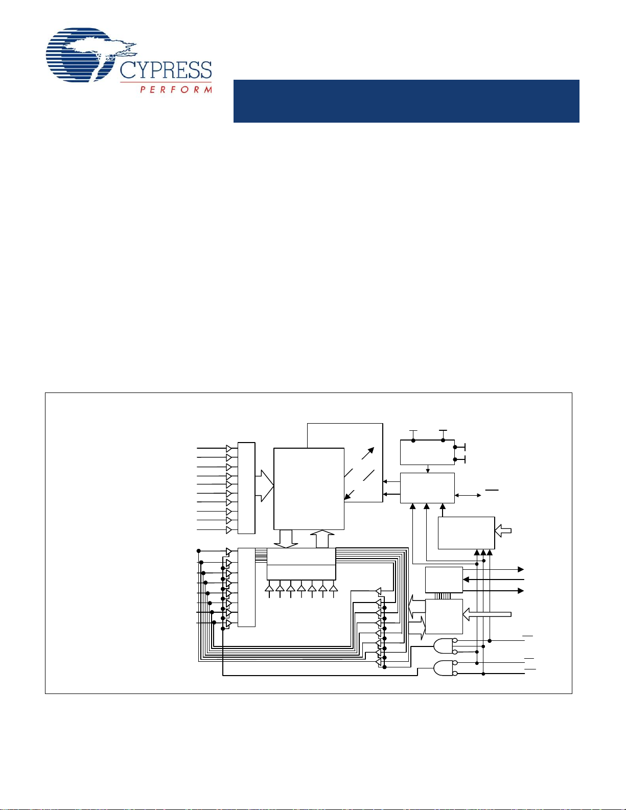
Logic Block Diagram
ROW DECODER INPUT BUFFERS
COLUMN DEC
G
E
W
COLUMN I/O
POWER
CONTROL
HSB
STORE/
RECALL
CONTROL
SOFTWARE
DETECT
A15 – A
0
A
5
A
6
A
7
A
8
A
9
A
12
A
13
A
14
A
15
A
16
Quantum Trap
1024 X 1024
STATIC RAM
ARRAY
1024 X 1024
STORE
RECALL
DQ
0
DQ
1
DQ
2
DQ
3
DQ
4
DQ
5
DQ
6
DQ
7
A0 A1 A2 A3 A4 A10 A
11
V
CC
V
CAP
RTC
MUX
A16 – A
0
X
1
X
2
INT
V
RTCbat
V
RTCcap
Description
■ nvSRAM Combined with Integrated Real Time Clock Functions
(RTC, Watchdog Timer, Clock Alarm, Power Monitor)
■ Capacitor or Battery Backup for RTC
■ 25, 45 ns Read Access and Read/Write Cycle Time
■ Unlimited Read/Write Endurance
■ Automatic nonvolatile STORE on Power Loss
■ Nonvolatile STORE Under Hardware or Software Control
■ Automatic RECALL to SRAM on Power Up
■ Unlimited RECALL Cycles
■ 200K STORE Cycles
■ 20-Year nonvolatile Data Retention
■ Single 3 V +20%, -10% Power Supply
■ Commercial and Industrial Temperatures
■ 48-pin 300-mil SSOP Package (RoHS-Compliant)
The Cypress STK17TA8 combines a 1 Mb nonvolatile static RAM
(nvSRAM) with a full featured real time clock in a reliable,
monolithic integrated circuit.
The 1 Mb nvSRAM is a fast static RAM with a nonvolatile
Quantum Trap storage element included with each memory cell.
The SRAM provides the fast access and cycle times, ease of use
and unlimited read and write endurance of a normal SRAM. Data
transfers automatically to the nonvolatile storage cells when
power loss is detected (the STORE operation). On power up,
data is automatically restored to the SRAM (the RECALL
operation). Both STORE and RECALL operations are also
available under software control.
The real time clock function provides an accurate clock with leap
year tracking and a programmable, high accuracy oscillator. The
Alarm function is programmable for one-time alarms or periodic
minutes, hours, or days alarms. There is also a programmable
watchdog timer for processor control.
Cypress Semiconductor Corporation • 198 Champion Court • San Jose, CA 95134-1709 • 408-943-2600
Document #: 001-52039 Rev. ** Revised March 02, 2009
[+] Feedback
STK17TA8
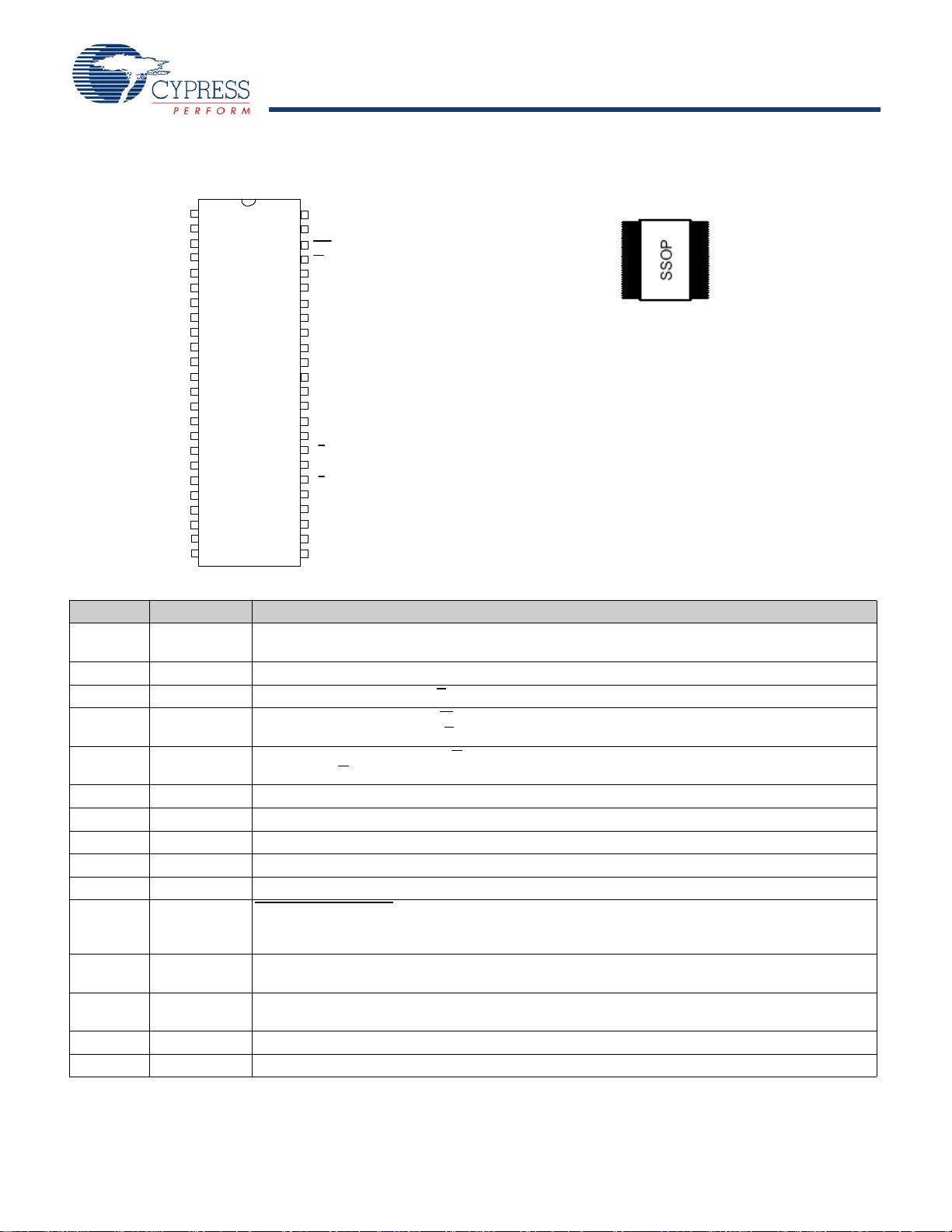
Pinouts
V
SS
A
14
A
12
A
7
A
6
DQ
0
DQ
1
V
CC
DQ
2
A
3
A
2
A
1
V
CAP
A
13
A
8
A
9
A
11
A
10
DQ
7
DQ
6
V
SS
A
0
NC
44
43
42
41
40
39
38
37
36
35
34
33
32
31
30
29
28
27
26
25
1
2
3
4
5
6
7
8
9
10
11
12
13
14
15
16
17
18
19
20
21
22
NC
X
1
X
2
23
24
A
5
INT
NC
NC
NC
NC
A
4
48
47
46
45
V
CC
HSB
NC
NC
W
NC
DQ
5
DQ
3
DQ
4
V
RTCbat
V
RTCcap
A
16
A
15
E
G
(TOP)
Note
1. For detailed package size specifications, See “Package Diagrams” on page 22..
Figure 1. Pin Diagram - 48-PIn SSOP
Pin Descriptions
Pin Name IO Type Description
A
16-A0
DQ
-DQ
7
0
E Input Chip Enable: The active low E
W Input Write Enable: The active low W
G Input Output Enable: The active low G input enables the data output buffers during read cycles.
X
1
X
2
V
RTCcap
V
RTCbat
V
CC
HSB I/O Hardware Store Busy
INT Output Interrupt Control: Can be programmed to respond to the clock alarm, the watchdog timer and the
V
CAP
V
SS
NC No Connect Unlabeled pins have no internal connections.
Document #: 001-52039 Rev. ** Page 2 of 23
Input Address: The 17 address inputs select one of 131,072 bytes in the nvSRAM array or one of 16 bytes
in the clock register map
I/O Data: Bi-directional 8-bit data bus for accessing the nvSRAM and RTC
selected on the falling edge of E
De-asserting G
high caused the DQ pins to tri-state.
Output Crystal Connection, drives crystal on startup
Input Crystal Connection for 32.768 kHz crystal
Power Supply Capacitor supplied backup RTC supply voltage (Left unconnected if V
Power Supply Battery supplied backup RTC supply voltage (Left unconnected if V
Power Supply Power: 3.0V, +20%, -10%
Power Supply Autostore™ Capacitor: Supplies power to nvSRAM during power loss to store data from SRAM to
Power Supply Ground
to the chip, it will initiate a nonvolatile STORE operation. A weak pull up resistor keeps this pin high if
not connected. (Connection Optional).
power monitor. Programmable to either active high (push/pull) or active low (open-drain)
nonvolatile storage elements.
Relative PCB Area Usage
[1]
input selects the device
enables data on the DQ pins to be written to the address location
is used)
RTCbat
is used)
RTCcap
: When low this output indicates a Store is in progress. When pulled low external
[+] Feedback
STK17TA8
Absolute Maximum Ratings
Voltage on Input Relative to Ground ................–0.1V to 4.1V
Voltage on Input Relative to V
Voltage on DQ
or HSB.....................–0.5V to (VCC + 0.5V)
0-7
.........–0.5V to (VCC + 0.5V)
SS
Temperature under Bias ............................... –55°C to 125°C
Junction Temperature ................................... –55°C to 140°C
Storage Temperature.................................... –65°C to 150°C
Power Dissipation.............................................................1W
DC Output Current (1 output at a time, 1s duration)..... 15mA
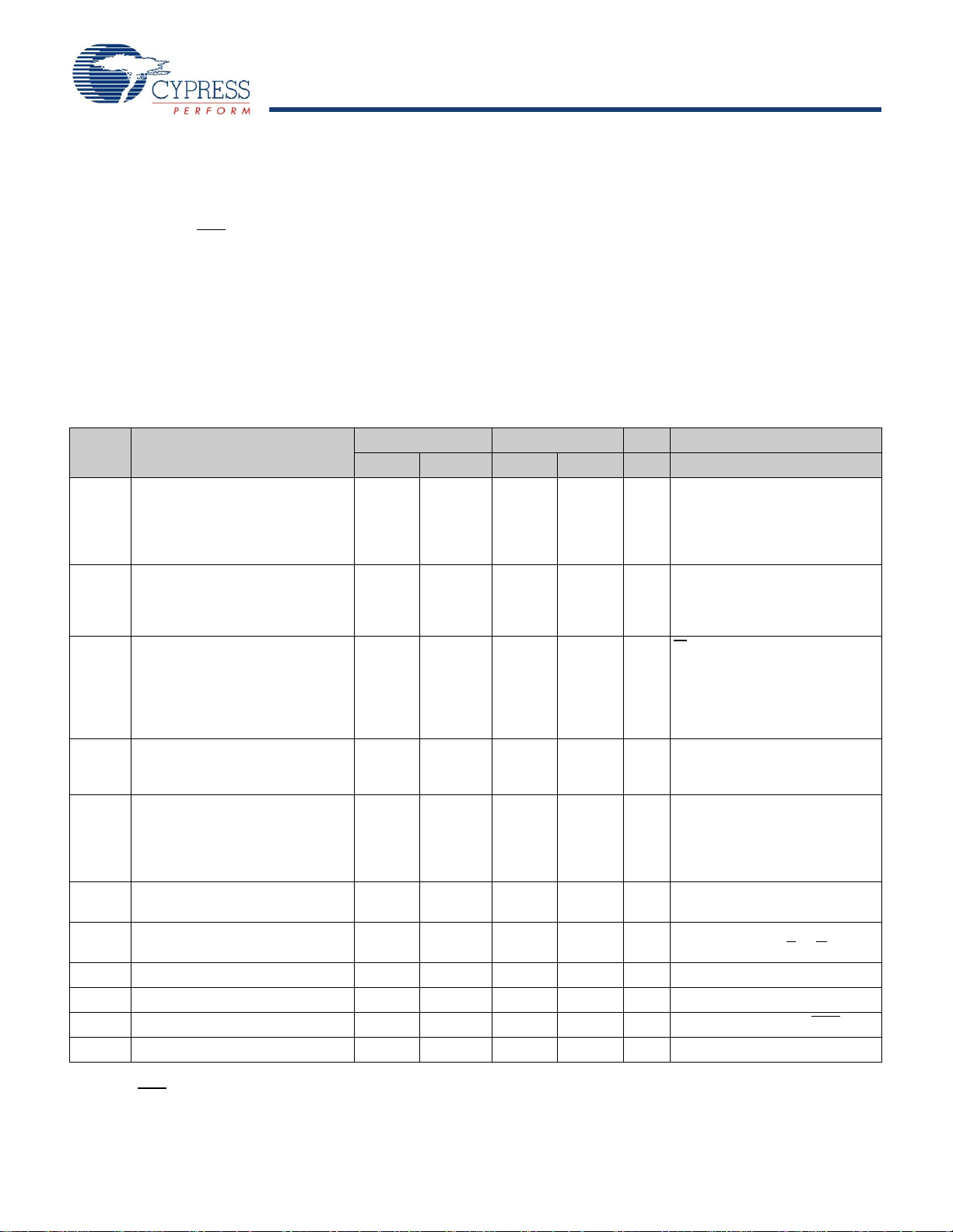
DC Electrical Characteristics
(VCC = 2.7V-3.6V)
RF (SSOP-48) Package Thermal Characteristics
θjc 6.2 C/W; θja 51.1 [0fpm], 44.7 [200fpm], 41.8 C/W [500fpm]
Note: Stresses greater than those listed under “Absolute
Maximum Ratings” may cause permanent damage to the device.
This is a stress rating only, and functional operation of the device
at conditions above those indicated in the operational sections
of this specification is not implied. Exposure to absolute
maximum rating conditions for extended periods may affect
reliablity.
Symbol Parameter
I
CC
I
CC
I
CC
Average VCC Current 65
1
Average VCC Current during
2
STORE
3
Average V
200ns
Current at t
CC
3V, 25°C, Typical
I
CC
I
SB
I
ILK
I
OLK
V
V
V
V
IH
IL
OH
OL
Average V
4
<Emphasis>AutoStore™ Cycle
V
Standby Current
CC
(Standby, Stable CMOS Levels)
Current during
CAP
Input Leakage Current ±1 ±1 mA V
Off-State Output Leakage Current ±1 ±1 mA V
Input Logic “1” Voltage 2.0 VCC + 0.5 2.0 VCC + 0.5 V All Inputs
Input Logic “0” Voltage VSS –0.5 0.8 VSS –0.5 0.8 V All Inputs
Output Logic “1” Voltage 2.4 2.4 V I
Output Logic “0” Voltage 0.4 0.4 V I
AVAV
=
Commercial Industrial Units Notes
Min Max Min Max
50
70
55
mAmAt
= 25 ns
AVAV
= 45 ns
t
AVAV
Dependent on output loading and
cycle rate. Values obtained
without output loads.
3 3 mA All Inputs Don’t Care, VCC = max
Average current for duration of
STORE
cycle (t
10 10 mA W ≥ (V
All Other Inputs Cycling at CMOS
STORE
– 0.2V)
CC
)
Levels
Dependent on output loading and
cycle rate. Values obtained
without output loads.
3 3 mA All Inputs Don’t Care
Average current for duration of
STORE cycle (t
33mAE ≥ (VCC -0.2V)
All Others V
(V
-0.2V)
CC
Standby current level after
≤ 0.2V or ≥
IN
nonvolatile cycle complete
= max
CC
V
= VSS to V
IN
= max
CC
V
= VSS to VCC, E or G ≥ VIH
IN
= –2 mA (except HSB)
OUT
= 4 mA
OUT
CC
STORE
)
Note: The HSB
Note: The INT is open-drain and does not source or sink high current when interrupt Register bit D3 is below.
pin has I
=-10uA for VOH of 2.4V, this parameter is characterized but not tested.
OUT
Document #: 001-52039 Rev. ** Page 3 of 23
[+] Feedback
STK17TA8
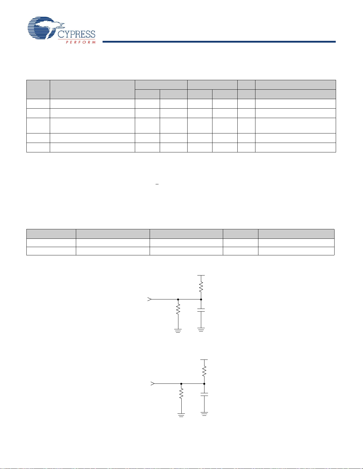
DC Electrical Characteristics (continued)
Notes
2. These parameters are guaranteed but not tested.
577 Ohms
30 pF
789 Ohms
3.0V
INCLUDING
SCOPE AND
OUTPUT
FIXTURE
577 Ohms
5 pF
789 Ohms
3.0V
INCLUDING
SCOPE AND
OUTPUT
FIXTURE
(V
= 2.7V-3.6V)
CC
Symbol Parameter
Commercial Industrial Units Notes
Min Max Min Max
T
V
V
NV
A
CC
CAP
Operating Temperature 0 70 –40 85 °C
Operating Voltage 2.7 3.6 2.7 3.6 V 3.0V +20%, -10%
Storage Capacitance 17 57 17 57 μF Between V
rated.
Nonvolatile STORE operations 200 200 K
C
DATARData Retention 20 20 Years At 55 °C
AC Test Conditions
Input Pulse Levels ....................................................0V to 3V
Input Rise and Fall Times ............................................ <
5 ns
Input and Output Timing Reference Levels.................... 1.5V
Output Load..................................See Figure 2 and Figure 3
Capacitance
(TA = 25°C, f = 1.0MHz)
Symbol
C
IN
C
OUT
[2]
Parameter Max Units Conditions
Input Capacitance 7 pF ΔV = 0 to 3V
Output Capacitance 7 pF ΔV = 0 to 3V
pin and VSS, 5V
CAP
Figure 3. AC Output Loading for Tristate Specs
Document #: 001-52039 Rev. ** Page 4 of 23
Figure 2. AC Output Loading
(tHZ, tLZ, t
WLQZ
, t
WHQZ
, t
, t
GLQX
GHQZ
[+] Feedback
STK17TA8
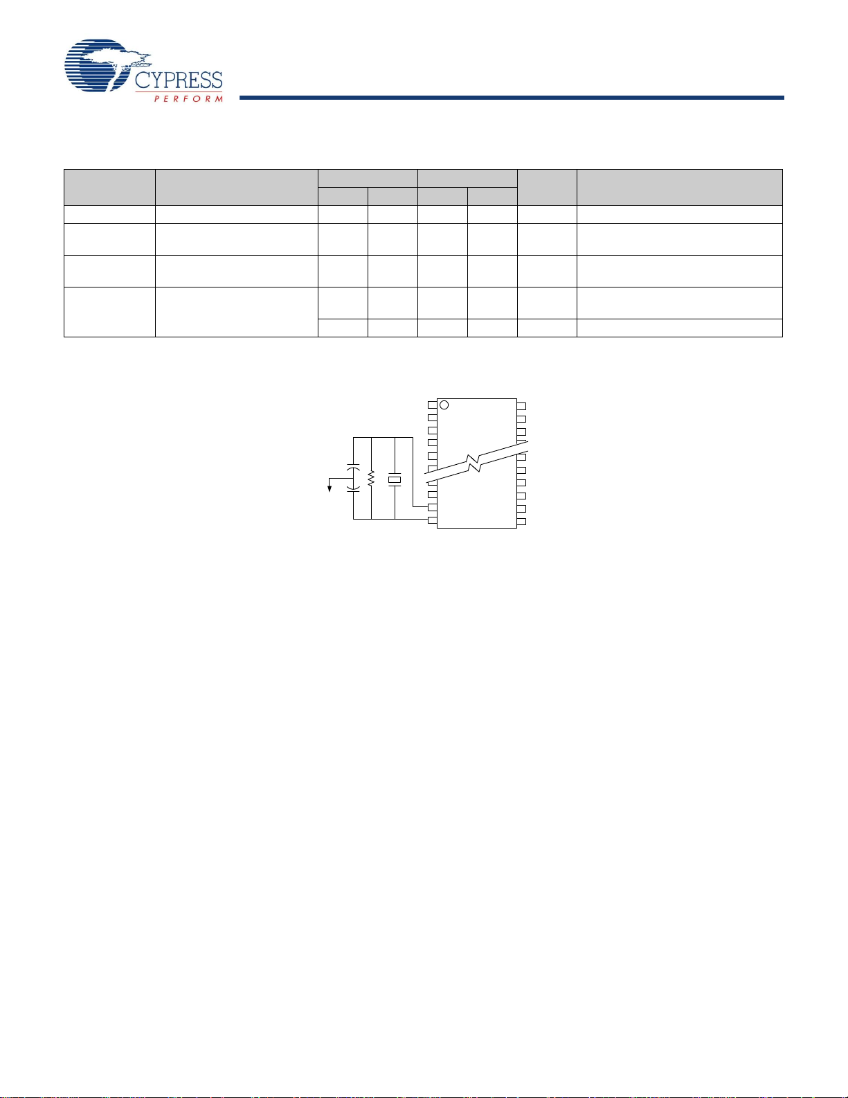
RTC DC Characteristics
C
1
C
2
RF
Y
1
X
1
X
2
Recommended Values
Y
1
= 32.768 KHz
= 10M Ohm
= 0 (install cap footprint,
but leave unloaded)
= 56 pF ± 10% (do not vary from this value)
RF
C
1
C
2
Symbol Parameter
I
BAK
RTC Backup Current — 300 — 350 nA From either V
Commercial Industrial
Min Max Min Max
Units Notes
RTCcap
or V
RTCbat
VRTCbat RTC Battery Pin Voltage 1.8 3.3 1.8 3.3 V Typical = 3.0 Volts during normal
operation
VRTCcap RTC Capacitor Pin Voltage 1.2 2.7 1.2 2.7 V Typical = 2.4 Volts during normal
operation
tOSCS RTC Oscillator time to start — 10 — 10 sec At MIN Temperature from Power up
or Enable
—5—5 secAt 25°C from Power up or Enable
Figure 4. RTC Recommended Component Configuration
Document #: 001-52039 Rev. ** Page 5 of 23
[+] Feedback
STK17TA8
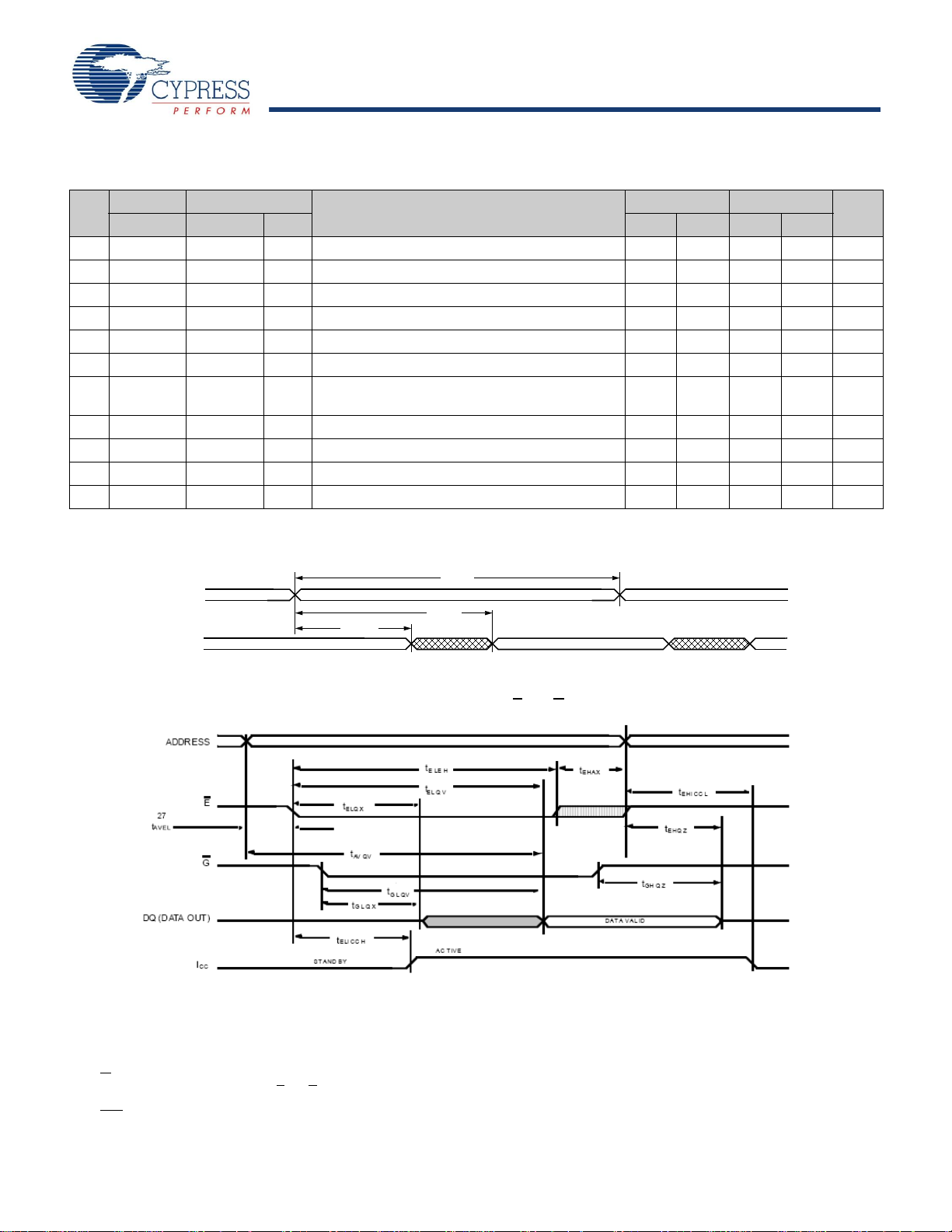
SRAM READ Cycles #1 and #2
Notes
3. W
must be high during SRAM READ cycles.
4. Device is continuously selected with E
and G both low
5. Measured ± 200mV from steady state output voltage.
6. HSB
must remain high during READ and WRITE cycles.
DATA VALID
5
t
AXQX
3
t
AVQ V
DQ (DATA OUT)
ADDRESS
2
t
AVAV
2
29
11
7
9
10
8
4
3
6
1
ELQV
t
ELEH
t
AVQ V
GLQV
t
AXQX
ELQX
EHQZ
GLQX
GHQZ
ELICCL
EHICCH
Symbols
[3]
[4]
[4]
[5]
[5]
[2]
[2]
NO.
#1 #2 Alt. Min Max Min Max
1t
AVAV
AVQ V
[3]
[4]
2t
3t
4t
AXQX
[4]
5t
6t
7t
8t
9t
10 t
11 t
Parameter
t
t
t
t
t
t
t
t
t
t
t
Chip Enable Access Time 25 45 ns
ACS
Read Cycle Time 25 45 ns
RC
Address Access Time 25 45 ns
AA
Output Enable to Data Valid 12 20 ns
OE
Output Hold after Address Change 3 3 ns
OH
Address Change or Chip Enable to Output Active 3 3 ns
LZ
Address Change or Chip Disable to Output
HZ
Inactive
Output Enable to Output Active 0 0 ns
OLZ
Output Disable to Output Inactive 10 15 ns
OHZ
Chip Enable to Power Active 0 0 ns
PA
Chip Disable to Power Standby 25 45 ns
PS
Figure 5. SRAM READ Cycle #1: Address Controlled
STK17TA8-25 STK17TA8-45
10 15 ns
[3, 4, 6]
Units
Document #: 001-52039 Rev. ** Page 6 of 23
Figure 6. SRAM READ Cycle #2: E and G Controlled
[3, 6]
[+] Feedback
STK17TA8
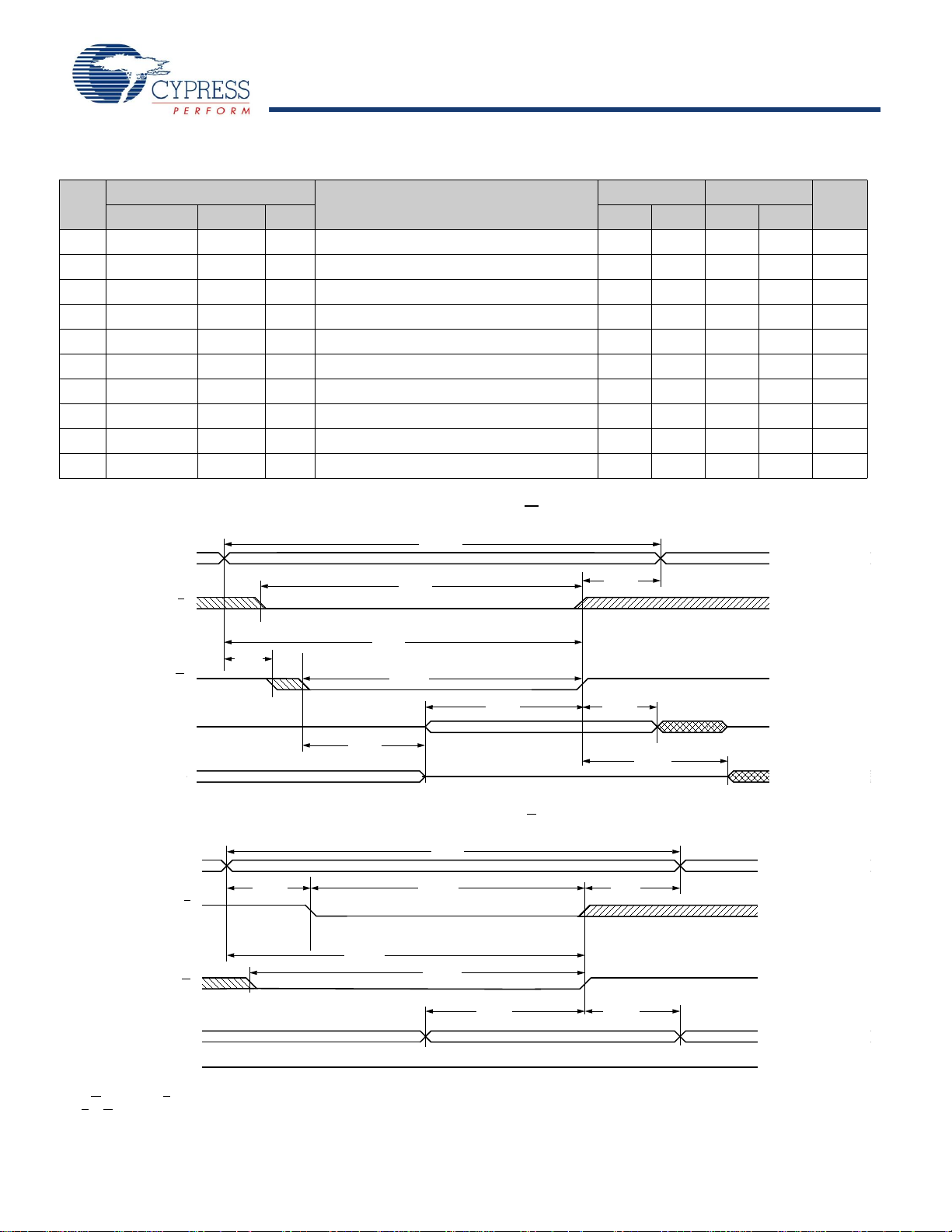
SRAM WRITE Cycles #1 and #2
Notes
7. If W
is low when E goes low, the outputs remain in the high-impedance state.
8.
E or W must be ≥ V
IH
during address transitions.
PREVIOUS DATA
DATA OUT
E
ADDRESS
11
t
AVAV
W
16
t
WHDX
DATA IN
19
t
WHAX
13
t
WLWH
18
t
AVW L
17
t
AVWH
DATA VALID
20
t
WLQZ
15
t
DVWH
HIGH IMPEDANCE
21
t
WHQX
14
t
ELWH
DATA IN
11
t
AVAV
16
t
EHDX
13
t
WLEH
19
t
EHAX
18
t
AVE L
17
t
AVE H
DATA VALID
15
t
DVEH
HIGH IMPEDANCE
14
t
ELEH
DATA OUT
E
ADDRESS
W
DATA IN
NO.
11 t
13 t
14 t
15 t
16 t
17 t
18 t
19 t
20 t
21 t
Symbols
Parameter
STK17TA8-25 STK17TA8-45
#1 #2 Alt. Min Max Min Max
AVAV
WLWH
ELWH
DVWH
WHDX
AVW H
AVW L
WHAX
WLQZ
WHQX
5, 7
t
AVAV
t
WLEH
t
ELEH
t
DVEH
t
EHDX
t
AVEH
t
AVEL
t
EHAX
t
t
t
t
t
t
t
t
t
t
Write Cycle Time 25 45 ns
WC
Write Pulse Width 20 30 ns
WP
Chip Enable to End of Write 20 30 ns
CW
Data Set-up to End of Write 10 15 ns
DW
Data Hold after End of Write 0 0 ns
DH
Address Set-up to End of Write 20 30 ns
AW
Address Set-up to Start of Write 0 0 ns
AS
Address Hold after End of Write 0 0 ns
WR
Write Enable to Output Disable 10 15 ns
WZ
Output Active after End of Write 3 3 ns
OW
Figure 7. SRAM WRITE Cycle #1: W Controlled
[7, 8]
Units
Document #: 001-52039 Rev. ** Page 7 of 23
Figure 8. SRAM WRITE Cycle #2: E Controlled
[7, 8]
[+] Feedback
 Loading...