

Page 1
STK14D88
32Kx8 AutoStore™ nvSRAM
Features
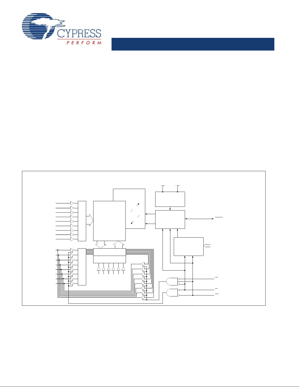
A0 A1 A2 A3 A4 A
10
COLUMN I/O
COLUMN DEC
STATIC RAM
ARRAY
512 x 512
ROW DECODER
INPUT BUFFERS
Quantum Trap
512 x 512
STORE/
RECALL
CONTROL
STORE
RECALL
POWER
CONTROL
A
5
A
6
A
7
A
8
A
9
A
11
A
12
A
13
A
14
DQ
0
DQ
1
DQ
2
DQ
3
DQ
4
DQ
5
DQ
6
DQ
7
SOFTWARE
DETECT
G
E
W
HSB
V
CCXVCAP
A0 - A
13
Logic Block Diagram
Description
■ 25, 35, 45 ns Read Access and R/W Cycle Time
■ Unlimited Read/Write Endurance
■ Automatic Nonvolatile STORE on Power Loss
■ Nonvolatile STORE Under Hardware or Software Control
■ Automatic RECALL to SRAM on Power Up
■ Unlimited RECALL Cycles
■ 200K STORE Cycles
■ 20-Year Nonvolatile Data Retention
■ Single 3.0V +20%, -10% Power Supply
■ Commercial, Industrial Temperatures
■ Small Footprint SOIC and SSOP Packages (RoHS-Compliant)
The Cypress STK14D88 is a 256Kb fast static RAM with a
nonvolatile Quantum Trap™ storage element included with each
memory cell.
The SRAM provides fast access and cycle times, ease of use,
and unlimited read and write endurance of a normal SRAM.
Data transfers automatically to the nonvolatile storage cells
when power loss is detected (the STORE operation). On power
up, data is automatically restored to the SRAM (the RECALL
operation). Both STORE and RECALL operations are also
available under software control.
The Cypress nvSRAM is the first monolithic nonvolatile memory
to offer unlimited writes and reads. It is the highest performance,
most reliable nonvolatile memory available.
Cypress Semiconductor Corporation • 198 Champion Court • San Jose, CA 95134-1709 • 408-943-2600
Document Number: 001-52037 Rev. ** Revised March 02, 2009
[+] Feedback
Page 2
STK14D88
Pin Configurations
48-Pin SSOP
TOP
V
SS
A
14
A
12
A
7
A
6
DQ
0
DQ
1
V
CC
DQ
2
A
3
A
2
A
1
V
CAP
A
13
A
8
A
9
A
11
A
10
DQ
7
DQ
6
V
SS
A
0
NC
44
43
42
41
40
39
38
37
36
35
34
33
32
31
30
29
28
27
26
25
1
2
3
4
5
6
7
8
9
10
11
12
13
14
15
16
17
18
19
20
21
22
NC
E
NC
NC
23
24
A
5
NC
NC
NC
NC
NC
NC
A
4
48
47
46
45
V
CC
HSB
NC
NC
W
NC
NC
DQ
5
DQ
3
DQ
4
G
NC NC
32-SOIC
TOP
V
SS
A
14
A
12
A
7
A
6
DQ
0
V
CAP
A
13
A
8
A
9
A
11
28
27
26
25
24
23
22
21
20
19
18
17
1
2
3
4
5
6
7
8
9
10
11
12
13
14
15
16
A
5
A
4
32
31
30
29
V
CC
HSB
W
A
3
A
2
A
1
A
0
DQ
1
DQ
2
A
10
DQ
7
DQ
5
DQ
3
DQ
4
DQ
6
NCNC
E
G
SSOP
Relative PCB Area Usage
[1]
Note
1. See “Package Diagrams” on page 15 for detailed package size specifications.
Figure 1. Pin Diagram 48-Pin SSOP/32-SOIC
Pin Descriptions
Pin Name I/O Description
A
14-A0
DQ
V
HSB
V
V
Document Number: 001-52037 Rev. ** Page 2 of 17
-DQ
7
0
E
W
G Input Output Enable: The active low G input enables the data output buffers during read cycles.
CC
CAP
SS
NC No Connect Unlabeled pins have no internal connections.
Input Address: The 15 address inputs select one of 32,768 bytes in the nvSRAM array
I/O Data: Bi-directional 8-bit data bus for accessing the nvSRAM
Input Chip Enable: The active low E input selects the device
Input Write Enable: The active low W enables data on the DQ pins to be written to the address location
Power Supply Power: 3.0V, +20%, -10%
I/O Hardware Store Busy: When low this output indicates a Store is in progress. When pulled low
Power Supply AutoStore™ Capacitor: Supplies power to nvSRAM during power loss to store data from SRAM to
Power Supply Ground
latched by the falling edge of E
De-asserting G
high caused the DQ pins to tri-state.
external to the chip, it will initiate a nonvolatile STORE operation. A weak pull up resistor keeps this
pin high if not connected. (Connection Optional).
nonvolatile storage elements.
[+] Feedback
Page 3
STK14D88
Absolute Maximum Ratings
Note:
2. The HSB
pin has I
OUT
=-10uA for VOH of 2.4V , this parameter is characterized but not tested
Voltage on Input Relative to Ground.................–0.5V to 4.1V
Voltage on Input Relative to V
Voltage on DQ
or HSB................. ... ..–0.5V to (VCC + 0.5V)
0-7
...........–0.6V to (VCC + 0.5V)
SS
Temperature under Bias............................... –55°C to 125°C
Storage Temperature.................................... –65°C to 140°C
Power Dissipation.............................................................1W
DC Output Current (1 output at a time, 1s duration).....15mA
NF (SOP-32) PACKAGE THERMAL CHARACTERISTICS
θ
5.4 C/W; θja 44.3 [0fpm], 37.9 [200fpm], 35.1 C/W [500fpm].
jc
RF (SSOP-48) PACKAGE THERMAL CHARACTERISTICS
θ
6.2 C/W; θja 51.1 [0fpm], 44.7 [200fpm], 41.8 C/W [500fpm].
jc
DC Characteristics
(VCC = 2.7V-3.6V)
Symbol Parameter
I
CC
I
CC
I
CC
Average VCC Current 65
1
Average VCC Current during
2
STORE
3
Average V
200ns
Current at t
CC
3V, 25°C, Typi ca l
I
CC
I
SB
Average V
4
AutoStore Cycle
V
CC
(Standby, Stable CMOS Input
CAP
Standby Current
Current during
Levels)
I
ILK
I
OLK
V
V
V
IH
IL
OH
Input Leakage Current ±1 ±1 μAV
Off-State Output Leakage Current ±1 ±1 μAV
Input Logic “1” Voltage 2.0 VCC + .5 2.0 VCC + .5 V All Inputs
Input Logic “0” Voltage VSS – .5 0.8 VSS – .5 0.8 V All Inputs
Output Logic “1” Voltage 2.4 2.4 V I
[2]
=
AVAV
Commercial Industrial
Min Max Min Max
Note: Stresses greater than those listed under “Absolute
Maximum Ratings” may cause permanent damage to the device.
This is a stress rating only, and functional operation of the device
at conditions above those indicated in the operational section s
of this specification is not implied. Exposure to absolute
maximum rating conditions for extended periods may affect
reliability.
Unit Notes
t
mA
mA
mA
= 25ns
AVAV
t
= 35ns
AVAV
t
= 45ns
AVAV
Dependent on output loading and
55
50
70
60
55
cycle rate. Values obtained without
output loads.
3 3 mA All Inputs Don’t Care, VCC = max
Average current for duration of
STORE cycle (t
10 10 mA W
All Others Cycling, CMOS Levels
≥ (V
CC
– 0.2V)
STORE
)
Dependent on output loading and
cycle rate. Values obtained without
output loads.
3 3 mA All Inputs Don’t Care
Average current for duration of
STORE cycle (t
STORE
)
33mAE ≥ (VCC – 0.2V)
All Others V
0.2V)
≤ 0.2V or ≥ (VCC –
IN
Standby current level after nonvolatile cycle complete
= max
CC
V
= VSS to V
IN
= max
CC
V
= VSS to VCC, E or G ≥ VIH
IN
= –2mA
OUT
CC
Document Number: 001-52037 Rev. ** Page 3 of 17
[+] Feedback
Page 4
STK14D88
DC Characteristics (continued)
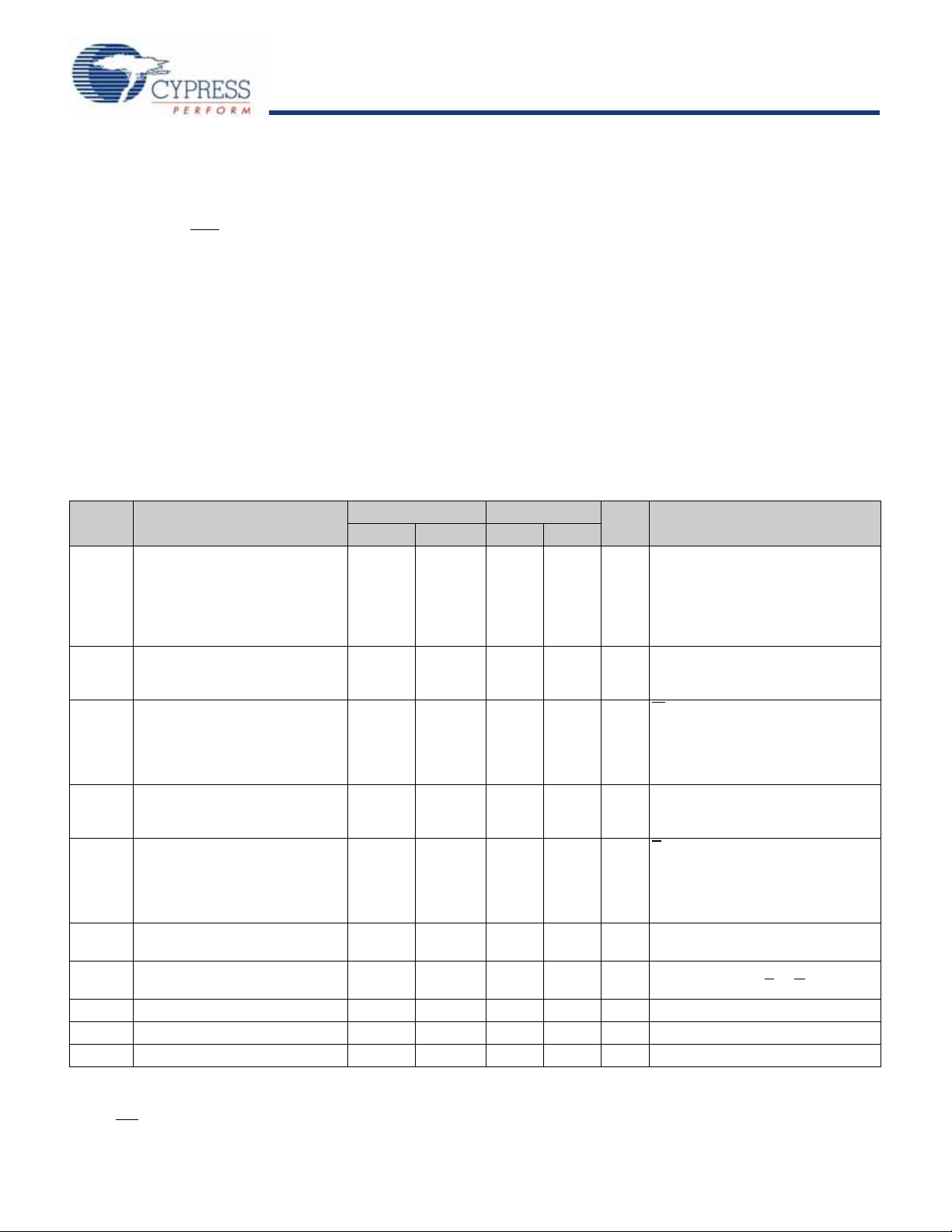
Input Pulse Levels....................................................0V to 3V
Input Rise and Fall Times ............................................ <5 ns
Input and Output Timing Reference Levels.................... 1.5V
Output Load..................................See Figure 2 and Figure 3
577
Ω
30 pF
789
Ω
3.0V
INCLUDING
SCOPE AND
OUTPUT
FIXTURE
577
Ω
5 pF
789
Ω
3.0V
INCLUDING
SCOPE AND
OUTPUT
FIXTURE
Note
3. These
parameters are guaranteed but not tested.
(VCC = 2.7V-3.6V)
Symbol Parameter
V
OL
T
A
V
CC
V
CAP
DATA
NV
Output Logic “0” Voltage 0.4 0.4 V I
Operating Temperature 0 70 -40 85 °C
Operating Voltage 2.7 3.6 2.7 3.6 V 3.3V +20%, -10%
Storage Capacitance 17 120 17 120 μFBetween V
Data Retention 20 20 K
R
Nonvolatile STORE Operations 200 200 Years @ 55°C
C
AC Test Conditions
[2]
Commercial Industrial
Min Max Min Max
Unit Notes
= 4mA
OUT
pin and VSS, 5V
Rated
CAP
Figure 2. AC Output Loading
Figure 3. AC Output Loading for Tri-state Specs (t
Capacitance
[3]
Description Test Conditions Max Unit Conditions
Input Capacitance TA = 25°C, f = 1 MHz, 7 pF ΔV = 0 to 3V
Output Capacitance 7 pF ΔV = 0 to 3V
Parameter
C
IN
C
OUT
Document Number: 001-52037 Rev. ** Page 4 of 17
, tLZ, t
HZ
WLQZ
, t
WHQZ
, t
, t
GLQX
GHQZ
[+] Feedback
Page 5
STK14D88
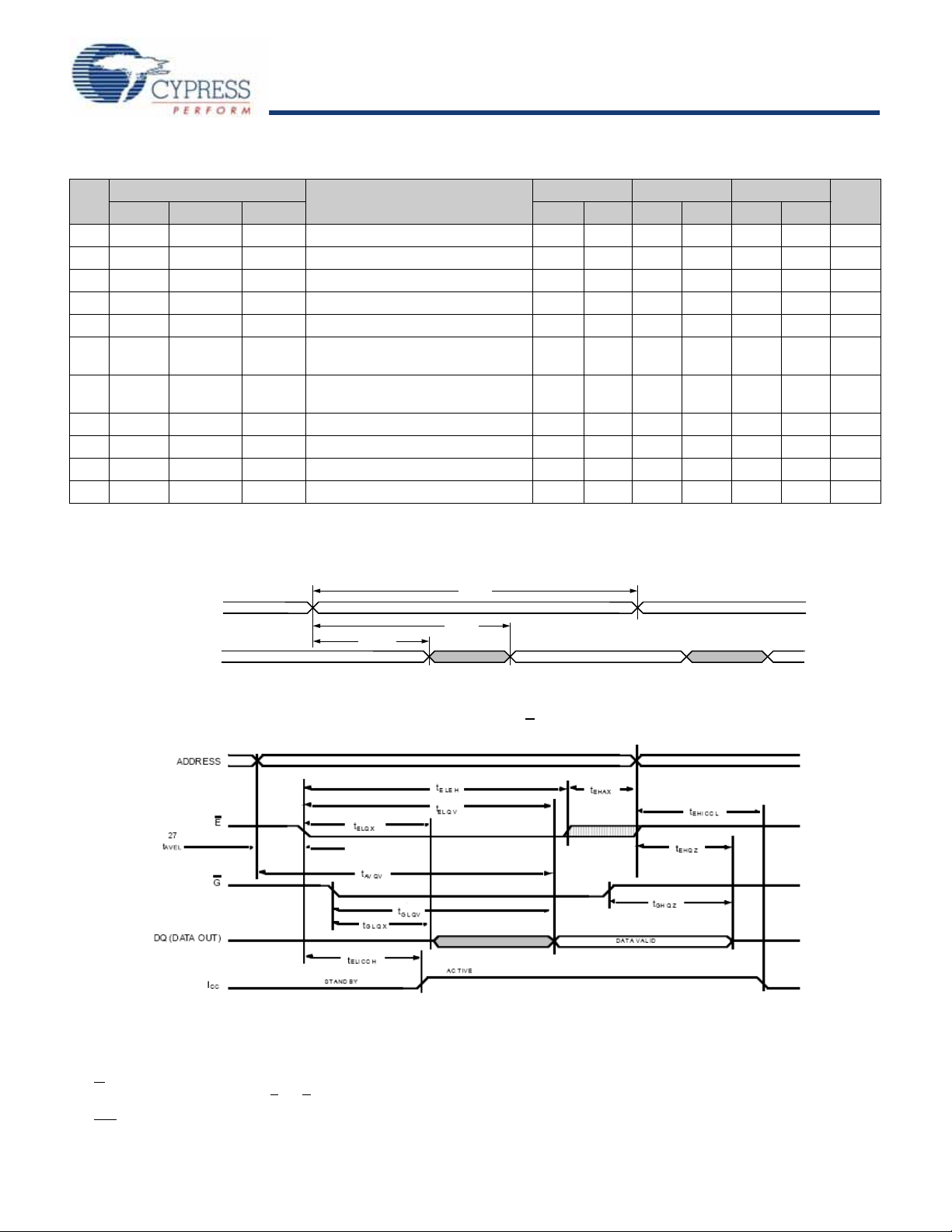
SRAM READ Cycles #1 and #2
Notes
4. W
must be high during SRAM READ cycles.
5. Device is continuously selected with E
and G both low.
6. Measured ± 200mV from steady state output voltage.
7. HSB
must remain high during READ and WRITE cycles.
DATA VALID
5
t
AXQX
3
t
AVQV
DQ (DATA OUT)
ADDRESS
2
t
AVAV
2
29
11
7
9
10
8
4
3
6
1
[4]
[5]
[5]
Symbols
ELQV
[4]
tELEH
[5]
t
AVQV
GLQV
[5]
t
AXQX
ELQX
[6]
EHQZ
GLQX
[6]
GHQZ
ELICCH
EHICCL
NO.
1t
2t
AVAV
3t
AVQV
4t
5t
AXQX
6t
7t
8t
9t
10 t
11 t
Parameter
t
ACS
t
RC
t
AA
t
OE
t
OH
t
LZ
t
HZ
t
OLZ
t
OHZ
[3]
t
PA
[3]
t
PS
Chip Enable Access Time 25 35 45 ns
Read Cycle Time 25 35 45 ns
Address Access Time 25 35 45 ns
Output Enable to Data Valid 12 15 20 ns
Output Hold after Address Change 3 3 3 ns
Address Change or Chip Enable to
Output Active
Address Change or Chip Disable to
Output Inactive
Output Enable to Output Active 0 0 0 ns
Output Disable to Output Inactive 10 13 15 ns
Chip Enable to Power Active 0 0 0 ns
Chip Disable to Power Standby 25 35 45 ns
Figure 4. SRAM READ Cycle 1: Address Controlled
STK14D88-25 STK14D88-35 STK14D88-45
Min Max Min Max Min Max#1 #2 Alt.
Unit
333ns
10 13 15 ns
[4, 5, 6]
Document Number: 001-52037 Rev. ** Page 5 of 17
Figure 5. SRAM READ Cycle 2: E Controlled
[4, 7]
[+] Feedback
Page 6
STK14D88
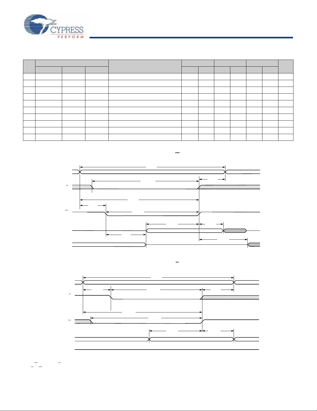
SRAM WRITE Cycle #1 and #2
DATA OUT
E
ADDRESS
W
DATA IN
PREVIOUS DATA
12
t
AVAV
13
t
WHDX
19
t
WHAX
13
t
WLWH
18
t
AVWL
17
t
AVWH
DATA VALID
20
t
WLQZ
15
t
DVWH
HIGH IMPEDANCE
21
t
WHQX
14
t
ELWH
12
t
AVAV
16
t
EHDX
13
t
WLEH
19
t
EHAX
18
t
AVEL
17
t
AVEH
DATA VALID
15
t
DVEH
HIGH IMPEDANCE
14
t
ELEH
DATA OUT
E
ADDRESS
W
DATA IN
Notes
8. If W
is low when E goes low, the outputs remain in the high-impedance state.
9. E
or W must be ≥ VIH during address transitions.
[6, 8]
Symbols
t
AVAV
t
WLEH
t
ELEH
t
DVEH
t
EHDX
t
AVEH
t
AVEL
t
EHAX
t
t
t
t
t
t
t
t
t
t
NO.
12 t
13 t
14 t
15 t
16 t
17 t
18 t
19 t
20 t
21 t
AVAV
WLWH
ELWH
DVWH
WHDX
AVWH
AVWL
WHAX
WLQZ
WHQX
Parameter
Write Cycle Time 25 35 45 ns
WC
Write Pulse Width 20 25 30 ns
WP
Chip Enable to End of Write 20 25 30 ns
CW
Data Set-up to End of Write 10 12 15 ns
DW
Data Hold after End of Write 0 0 0 ns
DH
Address Set-up to End of Write 20 25 30 ns
AW
Address Set-up to Start of Write 0 0 0 ns
AS
Address Hold after End of Write 0 0 0 ns
WR
Write Enable to Output Disable 10 13 15 ns
WZ
Output Active after End of Write 3 3 3 ns
OW
STK14D88-25 STK14D88-35 STK14D88-45
Min Max Min Max Min Max#1 #2 Alt.
Unit
Figure 6. SRAM WRITE Cycle 1: W
Controlled
Figure 7. SRAM WRITE Cycle 2: E Controlled
[8, 9]
[8, 9]
Document Number: 001-52037 Rev. ** Page 6 of 17
[+] Feedback
Page 7

STK14D88
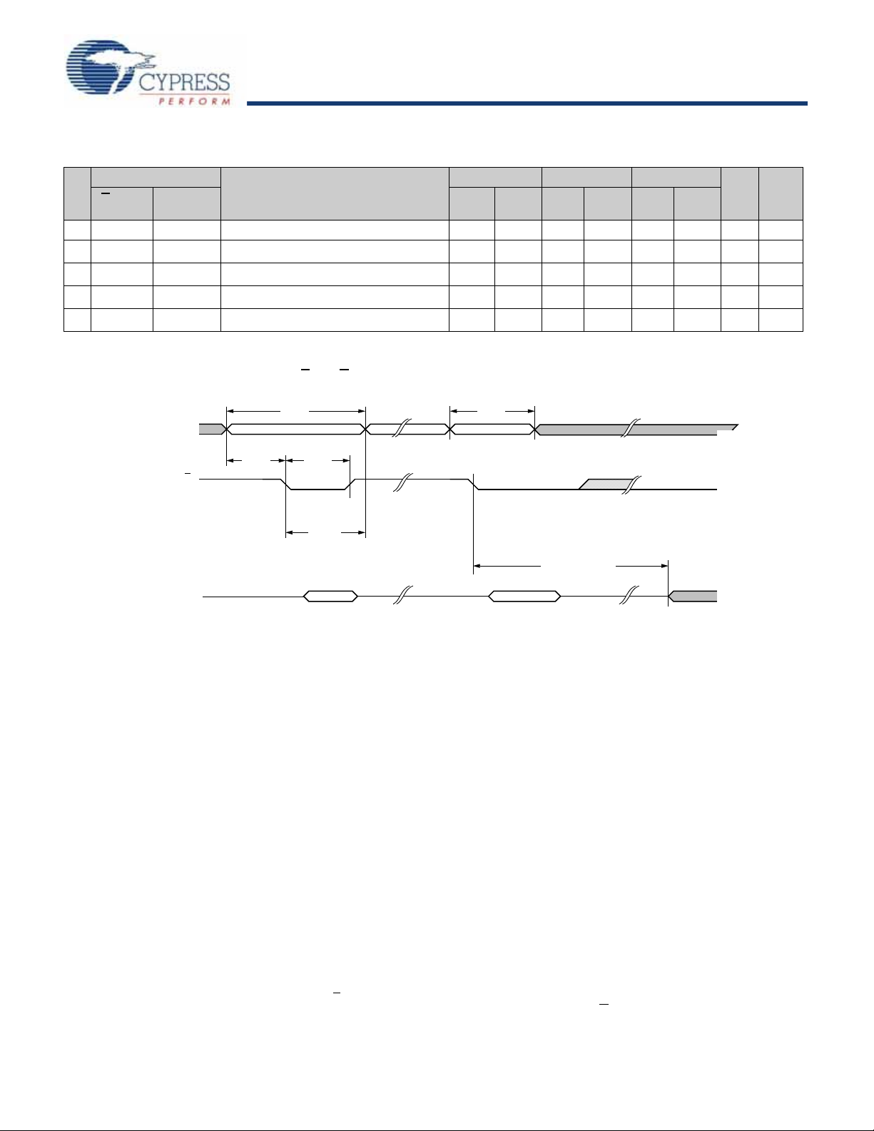
AutoStore/POWER UP RECALL
22
23
23
22
22
Notes
10.t
HRECALL
starts from the time VCC rises above V
SWITCH
.
11.If an SRAM WRITE has not taken place since the last nonvolatile cycle, no STORE will take pla ce.
12.Industrial Grade Devices require 15 ms Max.
No. Symbols Alt. Parameter
22 t
23 t
24 V
25 V
RECALL
STORE
SWITCH
CCRISE
t
HLHZ
Power up RECALL Duration 20 ms 10
STORE Cycle Duration 12.5 ms 11, 12
Low Voltage Trigger Level 2.65 V
Vcc Rise Time 150 μs
Figure 8. AutoStore /POWER UP RECALL
STK14D88
Min Max
Unit Notes
Note: Read and Write cycles are ignored during STORE, RECALL, and while V
Document Number: 001-52037 Rev. ** Page 7 of 17
is below V
CC
SWITCH
[+] Feedback
Page 8
STK14D88
Software-Controlled STORE/RECALL Cycle
DATA VALID
HIGH IMPEDANCE
ADDRESS #6ADDRESS #1
DATA VALID
26
t
AVAV
DATA VALID
DQ (DATA
E
ADDRESS
23 30
t
STORE
/ t
RECALL
26
t
AVAV
27
t
AVEL
28
t
ELEH
29
t
ELAX
Notes
13.The software sequence is clocked on the falling edge of E
controlled READs.
14.The six consecutive addresses must be read in the order listed in the software STORE/RECALL Mode Selection Table. W
must be high during all six consecutive cycles.
No.
Symbols
E Cont
Alternate
Parameter
[13, 14]
STK14D88-25 STK14D88-35 STK14D88-45
Min Max Min Max Min Max
Unit Notes
26 t
27
28
29
30
AVAV
t
AVEL
t
ELEH
t
EHAX
t
RECALL
t
t
t
RC
AS
CW
STORE/RECALL Initiation Cycle Time 25 35 45 ns 14
Address Setup Time 0 0 0 ns
Clock Pulse Width 20 25 30 ns
Address Hold Time 1 1 1 ns
RECALL Duration 50 50 50 μs
Figure 9. E
and G Controlled Software STORE/RECALL Cycle
[14]
Document Number: 001-52037 Rev. ** Page 8 of 17
[+] Feedback
Page 9

STK14D88
Hardware STORE Cycle
32
23
31
33 33
Notes
15.Read and Write cycles in progress before HSB
is asserted are given this minimum amount of time to complete.
16.This is the amount of time that it takes to take action on a soft sequence command. Vcc power must remain high to effectively register command.
17.Commands like Store and Recall lock out I/O until operation is complete which further increases this time. See specific command.
NO.
31 t
32 t
Symbols
Standard Alternate Min Max
DELAY
HLHX
t
HLQZ
Hardware STORE to SRAM Disabled 1 70 µs 15
Hardware STORE Pulse Width 15 ns
Parameter
STK14D88
Figure 10. Hardware STORE Cycle
Unit Notes
Soft Sequence Commands
NO.
33 t
Symbols
Standard Min Max
SS
Parameter
STK14D88
Unit Notes
Soft Sequence Processing Time 70 µs 16, 17
Figure 11. Software Sequence Commands
Document Number: 001-52037 Rev. ** Page 9 of 17
[+] Feedback
Page 10
STK14D88
Mode Selection
Notes
18.The six consecutive addresses must be in the order listed. W
must be high during all six consecutive cycles to enable a nonvolatile cycle.
19.While there are 15 addresses on the STK14D88, only the lower 14 are used to control software modes
20.I/O state depends on the state of G
. The I/O table shown assumes G low.
E W G A14–A
0
Mode IO Power Notes
H X X X Not Selected Output High Z Standby
L H L X Read SRAM Output Data Active
L L X X Write SRAM Input Data Active
L H L 0x0E38
0x31C7
0x03E0
0x3C1F
0x303F
0x03F8
L H L 0x0E38
0x31C7
0x03E0
0x3C1F
0x303F
0x07F0
L H L 0x0E38
0x31C7
0x03E0
0x3C1F
0x303F
0x0FC0 Nonvolatile Store Output High Z I
L H L 0x0E38
0x31C7
0x03E0
0x3C1F
0x303F
0x0C63
Read SRAM
Read SRAM
Read SRAM
Read SRAM
Read SRAM
AutoStore Disable
Read SRAM
Read SRAM
Read SRAM
Read SRAM
Read SRAM
AutoStore Enable
Read SRAM
Read SRAM
Read SRAM
Read SRAM
Read SRAM
Read SRAM
Read SRAM
Read SRAM
Read SRAM
Read SRAM
Nonvolatile Recall
Output Data
Output Data
Output Data
Output Data
Output Data
Output Data
Output Data
Output Data
Output Data
Output Data
Output Data
Output Data
Output Data
Output Data
Output Data
Output Data
Output Data
Output Data
Output Data
Output Data
Output Data
Output Data
Output High Z
Active 18, 19, 20
Active 18, 19, 20
Active
CC2
Active 18, 19, 20
18, 19, 20
Document Number: 001-52037 Rev. ** Page 10 of 17
[+] Feedback
Page 11
STK14D88
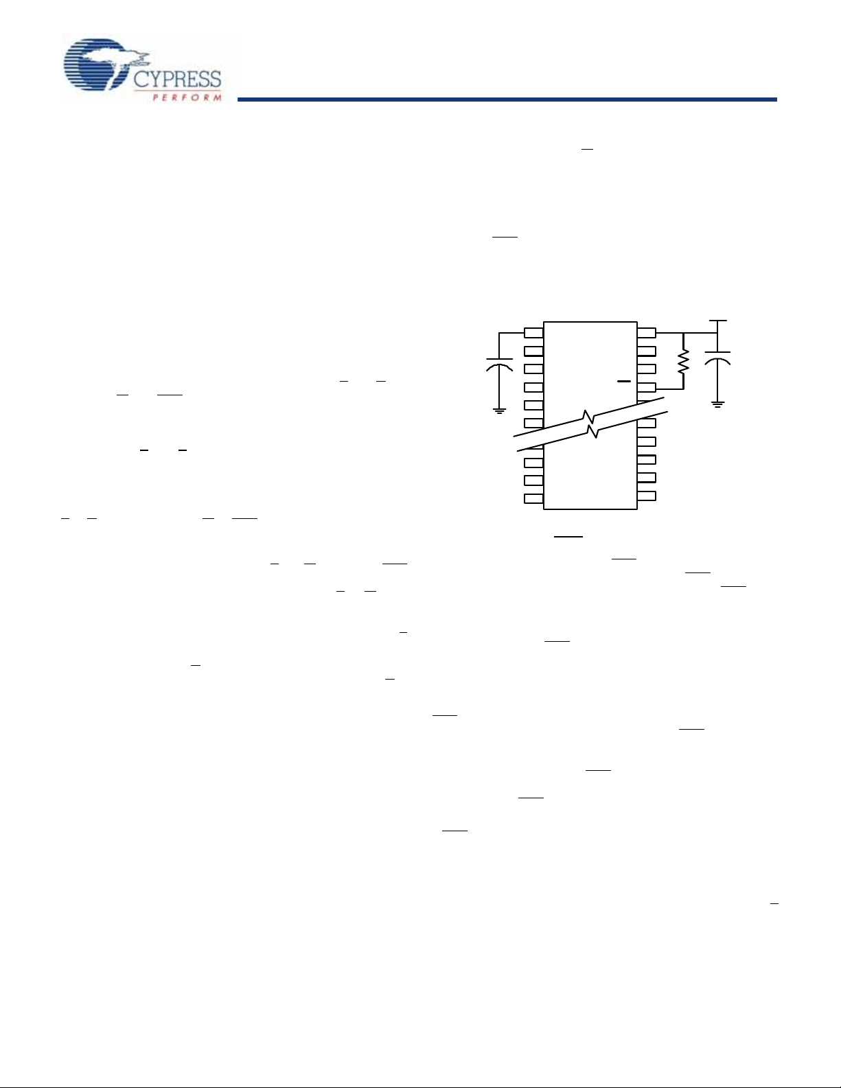
V
V
CC
V
CAP
10k Ohm
0.1µF
V
CC
V
CAP
W
nvSRAM Operation
nvSRAM
The STK14D88 nvSRAM is made up of two functional components paired in the same physical cell. These are the SRAM
memory cell and a nonvolatile QuantumTrap™ cell. The SRAM
memory cell operates like a standard fast static RAM. Data in the
SRAM can be transferred to the nonvolatile cell (the STORE
operation), or from the nonvolatile cell to SRAM (the RECALL
operation). This unique architecture allows all cells to be stored
and recalled in parallel. During the STORE and RECALL opera-
pin is driven to 5V by a charge pump internal to the chip. A
CAP
pull up should be placed on W
to hold it inactive during power up.
To reduce unneeded nonvolatile stores, AutoStore and
Hardware Store operations will be ignored unless at least one
WRITE operation has taken place since the most recent STORE
or RECALL cycle. Software initiated STORE cycles are
performed regardless of whether a WRITE operation has taken
place. The HSB
signal can be monitored by the system to detect
an AutoStore cycle is in progress.
Figure 12. AutoStore Mode
tions SRAM READ and WRITE operations are inhibited. The
STK14D88 supports unlimited read and writes like a typical
SRAM. In addition, it provides unlimited RECALL operations
from the nonvolatile cells and up to 200K STORE operations.
SRAM READ
The STK14D88 performs a READ cycle whenever E and G are
low while W
A
0-16
When the READ is initiated by an address transition, the outputs
will be valid after a delay of t
is initiated by E
t
GLQV
repeatedly respond to address changes within the t
time without the need for transitions on any control input pins,
and will remain valid until another address change or until either
E
or G is brought high, or W or HSB is brought low.
SRAM WRITE
A WRITE cycle is performed whenever E and W are low and HSB
is high. The address inputs must be stable prior to entering the
WRITE cycle and must remain stable until either E
high at the end of the cycle. The data on the common I/O pins
DQ
0-7
end of a W controlled WRITE or t
controlled WRITE.
It is recommended that G
cycle to avoid data bus contention on common I/O lines. If G
left low, internal circuitry will turn off the output buffers t
goes low.
W
AutoStore Operation
The STK14D88 stores data to nvSRAM using one of three
storage operations. These three operations are Hardware Store
(activated by HSB), Software Store (activated by an address
sequence), and AutoStore (on power down).
AutoStore operation is a unique feature of Cypress Quantum
Trap technology is enabled by default on the STK14D88.
During normal operation, the device will draw current from V
to charge a capacitor connected to the V
charge will be used by the chip to perform a single STORE
operation. If the voltage on the V
the part will automatically disconnect the V
STORE operation will be initiated with power provided by the
V
CAP
Figure 12 shows the proper connection of the storage capacitor
(V
CAP
TERISTICS table for the size of the capacitor. The voltage on the
and HSB are high. The address specified on pins
determine which of the 32,768 data bytes will be accessed.
(READ cycle #1). If the READ
, whichever is later (READ cycle #2). The data outputs will
and G, the o utputs will be valid at t
AVQV
ELQV
AVQV
or at
access
or W goes
will be written into memory if it is valid t
before the end of an E
DVEH
DVWH
before the
be kept high during the entire WRITE
after
WLQZ
pin. This stored
CAP
pin drops below VSWITCH,
CC
pin from VCC. A
CAP
CC
capacitor.
) for automatic store operation. Refer to the DC CHARAC-
Hardware STORE (HSB) Operation
The STK14D88 provides the HSB pin for controlling and
acknowledging the STORE operations. The HSB
used to request a hardware STORE cycle. When the HSB
driven low, the STK14D88 will conditionally initiate a STORE
operation after t
a WRITE to the SRAM took place since the last STORE or
RECALL cycle. The HSB
. An actual STORE cycle will only begin if
DELAY
pin has a very resistive pull up and is
internally driven low to indicate a busy condition while the
STORE (initiated by any means) is in progress. This pin should
is
be externally pulled up if it is used to drive other inputs.
SRAM READ and WRITE operations that are in progress when
HSB
is driven low by any means are given time to complete
before the STORE operation is initiated. After HSB
STK14D88 will continue SRAM operations for t
t
, multiple SRAM READ operations may take place. If a
DELAY
WRITE is in progress when HSB
a time, t
requested after HSB
, to complete. However, any SRAM WRITE cycles
DELAY
goes low will be inhibited until HSB returns
is pulled low, it will be allowed
high.
is not used, it should be left unconnected.
If HSB
Software STORE
Data can be transferred from the SRAM to the nonvolatile
memory by a software address sequence. The STK14D88
software STORE cycle is initiated by executing sequential E
controlled READ cycles from six specific address locations in
exact order. During the STORE cycle, previous data is erased
and then the new data is programmed into the nonvolatile
elements. Once a STORE cycle is initiated, further memory
inputs and outputs are disabled until the cycle is completed.
pin can be
pin is
goes low, the
. During
DELAY
Document Number: 001-52037 Rev. ** Page 11 of 17
[+] Feedback
Page 12

STK14D88
To initiate the software STORE cycle, the following READ
sequence must be performed:
1. Read Address 0x0E38, Valid READ
2. Read Address 0x31C7, Valid READ
3. Read Address 0x03E0, Valid READ
4. Read Address 0x3C1F, Valid READ
5. Read Address 0x303F, Valid READ
6. Read Address 0x0FC0, Initiate STORE Cycle
Once the sixth address in the sequence has been entered, the
STORE cycle will commence and the chip will be disabled. It is
important that READ cycles and not WRITE cycles be used in
the sequence. After the t
SRAM will again be activated for READ and WRITE operation.
cycle time has been fulfilled, the
STORE
Software RECALL
Data can be transferred from the nonvolatile memory to the
SRAM by a software address sequence. A software RECALL
cycle is initiated with a sequence of READ operations in a
manner similar to the software STORE initiation. To initiate the
RECALL cycle, the following sequence of E controlled READ
operations must be performed:
1. Read Address 0x0E38, Valid READ
2. Read Address 0x31C7, Valid READ
3. Read Address 0x03E0, Valid READ
4. Read Address 0x3C1F, Valid READ
5. Read Address 0x303F, Valid READ
6. Read Address 0x0C63, Initiate RECALL Cycle
Internally, RECALL is a two-step procedure. First, the SRAM
data is cleared, and second, the nonvolatile information is transferred into the SRAM cells. After the t
SRAM will once again be ready for READ or WRITE operations.
cycle time, the
RECALL
The RECALL operation in no way alters the data in the nonvolatile storage elements.
Data Protection
The STK14D88 protects data from corruption during low-voltage
conditions by inhibiting all externally initiated STORE and
WRITE operations. The low-voltage condition is detected when
V
CC<VSWITCH
If the STK14D88 is in a WRITE mode (both E
.
and W low) at
power-up, after a RECALL, or after a STORE, the WRITE will be
inhibited until a negative transition on E or W is de tected. This
protects against inadvertent writes during power up or brown out
conditions.
Best Practices
nvSRAM products have been used effectively for over 15 years.
While ease-of-use is one of the product’s main system values,
experience gained working with hundreds of applications has
resulted in the following suggestions as best practices:
■ The nonvolatile cells in an nvSRAM are programmed on the
test floor during final test and quality assurance. Incoming
inspection routines at customer or contract manufacturer’s
sites will sometimes reprogram these values. Final NV patterns
are typically repeating patterns of AA, 55, 00, FF, A5, or 5A.
End product’s firmware should not assume an NV array is in a
set programmed state. Routines that check memory content
values to determine first time system configuration, cold or
warm boot status, etc. should always program a unique NV
pattern (e.g., complex 4-byte pattern of 46 E6 49 53 hex or
more random bytes) as part of the final system manufacturing
test to ensure these system routines work consistently.
■ Power up boot firmware routines should rewrite the nvSRAM
into the desired state (autostore enabled, etc.). While the
nvSRAM is shipped in a preset state, best practice is to again
rewrite the nvSRAM into the desired state as a safeguard
against events that might flip the bit inadvertently (program
bugs, incoming inspection routines, etc.).
■ If AutoStore has been firmware disabled, it will not reset to
“autostore enabled” on every power down event captured by
the nvSRAM. The application firmware should re-enable or
re-disable autostore on each reset sequence based on the
behavior desired.
■ The V
and a maximum value size. Best practice is to meet this
requirement and not exceed the max V
nvSRAM internal algorithm calculates V
on this max V
V
CAP
time should discuss their V
understand any impact on the V
a t
value specified in this data sheet includes a minimum
CAP
value because the
CAP
charge time based
value. Customers that want to use a larger
value to make sure there is extra store charge and store
RECALL
CAP
period.
size selection with Cypress to
CAP
CAP
voltage level at the end of
CAP
Low Average Active Power
CMOS technology provides the STK14D88 with the benefit of
power supply current that scales with cycle time. Less current will
be drawn as the memory cycle time becomes longer than 50 ns.
Figure 13 shows the relationship between I
READ/WRITE cycle time. Worst-case current consumption is
shown for commercial temperature range, V
enable at maximum frequency. Only standby current is drawn
= 3.6V, and chip
CC
when the chip is disabled. The overall average current drawn by
the STK14D88 depends on the following items:
■ The duty cycle of chip enable
■ The overall cycle rate for operations
■ The ratio of READs to WRITEs
■ The operating temperature
■ The V
■ I/O loading
CC
level
CC
and
Document Number: 001-52037 Rev. ** Page 12 of 17
[+] Feedback
Page 13

STK14D88
Figure 13. Current versus Cycle Time
Average Active Current (mA)
100 150 200 300
0
10
20
30
40
50
Writes
Reads
Cycle Time (ns)
50
Noise Considerations
The STK14D88 is a high-speed memory and so must have a
high-frequency bypass capacitor of 0.1 µF connected between
both VCC pins and VSS ground plane with no plane break to chip
V
. Use leads and traces that are as short as possible. As with
SS
all high-speed CMOS ICs, careful routing of power, ground, and
signals will reduce circuit noise.
Preventing AutoStore
The AutoStore function can be disabled by initiating an
AutoStore Disable sequence. A sequence of READ operations
is performed in a manner similar to the software STORE initiation. To initiate the AutoStore Disable sequence, the following
sequence of E
be performed:
1. Read Address 0x0E38, Valid READ
2. Read Address 0x31C7, Valid READ
3. Read Address 0x03E0, Valid READ
4. Read Address 0x3C1F , Valid READ
5. Read Address 0x303F , Valid READ
6. Read Address 0x03F8, AutoStore Disable
The AutoStore can be re-enabled by initiating an AutoStore
Enable sequence. A sequence of READ operations is performed
in a manner similar to the software RECALL initiation. To initiate
the AutoStore Enable sequence, the following sequen ce of E
controlled or G controlled READ operations must be performed:
1. Read Address 0x0E38, Valid READ
2. Read Address 0x31C7, Valid READ
3. Read Address 0x03E0, Valid READ
4. Read Address 0x3C1F , Valid READ
5. Read Address 0x303F , Valid READ
6. Read Address 0x07F0, AutoStore Enable
If the AutoStore function is disabled or re-enabled, a manual
STORE operation (Hardware or Software) needs to be issued to
save the AutoStore state through subsequent power down
cycles. The part comes from the factory with AutoS tore enabled.
In all cases, make sure the READ sequence is uninterrupted. For
example, an interrupt that occurs in the sequence that reads the
nvSRAM would abort this sequence, resulting in an error.
controlled or G controlled READ operations must
Document Number: 001-52037 Rev. ** Page 13 of 17
[+] Feedback
Page 14

STK14D88
Part Numbering Nomenclature
Packaging Option:
TR = Tape and Reel
Blank = Tube
Speed:
25 - 25 ns
35 - 35 ns
Package:
N =
Plastic 32-pin 300 mil SOIC (50 mil pitch)
Temperature Range:
Blank - Commercial (0 to 70°C)
R =
Plastic 48-pin 300 mil SSOP(25 mil pitch)
Lead Finish
F = 100% Sn (Matte Tin) ROHS Compliant
45 - 45 ns
I - Industrial (-40 to 85°C)
STK14D88 - R F 45 I TR
Ordering Codes
Part Number Description Access Times Temperature
STK14D88-NF25 3V 32Kx8 AutoStore nvSRAM SOP32-300 25 ns Commercial
STK14D88-NF35 3V 32Kx8 AutoStore nvSRAM SOP32-300 35 ns Commercial
STK14D88-NF45 3V 32Kx8 AutoStore nvSRAM SOP32-300 45 ns Commercial
STK14D88-NF25TR 3V 32Kx8 AutoStore nvSRAM SOP32-300 25 ns Commercial
STK14D88-NF35TR 3V 32Kx8 AutoStore nvSRAM SOP32-300 35 ns Commercial
STK14D88-NF45TR 3V 32Kx8 AutoStore nvSRAM SOP32-300 45 ns Commercial
STK14D88-RF25 3V 32Kx8 AutoStore nvSRAM SSOP48-300 25 ns Commercial
STK14D88-RF35 3V 32Kx8 AutoStore nvSRAM SSOP48-300 35 ns Commercial
STK14D88-RF45 3V 32Kx8 AutoStore nvSRAM SSOP48-300 45 ns Commercial
STK14D88-RF25TR 3V 32Kx8 AutoStore nvSRAM SSOP48-300 25 ns Commercial
STK14D88-RF35TR 3V 32Kx8 AutoStore nvSRAM SSOP48-300 35 ns Commercial
STK14D88-RF45TR 3V 32Kx8 AutoStore nvSRAM SSOP48-300 45 ns Commercial
STK14D88-NF25I 3V 32Kx8 AutoStore nvSRAM SOP32-300 25 ns Industrial
STK14D88-NF35I 3V 32Kx8 AutoStore nvSRAM SOP32-300 35 ns Industrial
STK14D88-NF45I 3V 32Kx8 AutoStore nvSRAM SOP32-300 45 ns Industrial
STK14D88-NF25ITR 3V 32Kx8 AutoStore nvSRAM SOP32-300 25 ns Industrial
STK14D88-NF35ITR 3V 32Kx8 AutoStore nvSRAM SOP32-300 35 ns Industrial
STK14D88-NF45ITR 3V 32Kx8 AutoStore nvSRAM SOP32-300 45 ns Industrial
STK14D88-RF25I 3V 32Kx8 AutoStore nvSRAM SSOP48-300 25 ns Industrial
STK14D88-RF35I 3V 32Kx8 AutoStore nvSRAM SSOP48-300 35 ns Industrial
STK14D88-RF45I 3V 32Kx8 AutoStore nvSRAM SSOP48-300 45 ns Industrial
STK14D88-RF25ITR 3V 32Kx8 AutoStore nvSRAM SSOP48-300 25 ns Industrial
STK14D88-RF35ITR 3V 32Kx8 AutoStore nvSRAM SSOP48-300 35 ns Industrial
STK14D88-RF45ITR 3V 32Kx8 AutoStore nvSRAM SSOP48-300 45 ns Industrial
Document Number: 001-52037 Rev. ** Page 14 of 17
[+] Feedback
Page 15

STK14D88
Package Diagrams
PIN 1 ID
SEATING PLANE
116
17 32
DIMENSIONS IN INCHES[MM]
MIN.
MAX.
0.292[7.416]
0.299[7.594]
0.405[10.287]
0.419[10.642]
TYP.
0.090[2.286]
0.100[2.540]
0.004[0.101]
0.0100[0.254]
0.006[0.152]
0.012[0.304]
0.021[0.533]
0.041[1.041]
0.026[0.660]
0.032[0.812]
0.004[0.101]
REFERENCE JEDEC MO-119
PART #
S32.3 STANDARD PKG.
SZ32.3 LEAD FREE PKG.
0.014[0.355]
0.020[0.508]
0.810[20.574]
0.822[20.878]
51-85127 *A
Figure 14. 32-Pin (300 Mil) SOIC (51-85127)
Document Number: 001-52037 Rev. ** Page 15 of 17
[+] Feedback
Page 16

STK14D88
Package Diagrams (continued)
51-85061-*C
Figure 15. 48-Pin (300 Mil) SSOP (51-85061)
Document Number: 001-52037 Rev. ** Page 16 of 17
[+] Feedback
Page 17

STK14D88
Document History Page
Document Title: STK14D88 32Kx8 AutoStore™ nvSRAM
Document Number: 001-52037
Revision ECN
Orig. of
Change
Submission
Date
Description of Change
** 2668632 GVCH 03/04/2009 New data sheet
Sales, Solutions, and Legal Information
Worldwide Sales and Design Support
Cypress maintains a worldwide network of offices, solution centers, manufacturer’s representatives, and distributors. T o find the office
closest to you, visit us at cypress.com/sales.
Products
PSoC psoc.cypress.com
Clocks & Buffers clocks.cypress.com
Wireless wireless.cypress.com
Memories memory.cypress.com
Image Sensors image.cypress.com
PSoC Solutions
General psoc.cypress.com/solutions
Low Power/Low Voltage psoc.cypress.com/low-power
Precision Analog psoc.cypress.com/precision-analog
LCD Drive psoc.cypress.com/lcd-drive
CAN 2.0b psoc.cypress.com/can
USB psoc.cypress.com/usb
© Cypress Semiconductor Corporation, 2009. The information contained herein is subject to change without notice. Cypress Semiconductor Corporation assumes no responsibility for the use of any
circuitry other than circuitry embodied in a Cypress product. Nor does it convey or imply any license under patent or other rights. Cypress products are not warranted nor intend ed to be used for medica l,
life support, life saving, critical control or safety applications, unless pursuant to an express written agreement with Cypress. Furthermore, Cypress does not authorize its products for use as critical
components in life-support systems where a malfunction or failure may reasonably be expected to result in significant injury to the user. The inclusion of Cypress products in life-support systems
application implies that the manufacturer assumes all risk of such use and in doing so indemnifies Cypress against all charges.
Any Source Code (software and/or firmware) is owned by Cypress Semiconductor Corporation (Cypress) and is protected by and subject to worldwide patent protection (United States and foreign),
United States copyright laws and international treaty provisions. Cypress hereby gr ant s to l icense e a pers onal, no n-exclu sive , non-tr ansfer able license to copy, use, modify, create derivative works of,
and compile the Cypress Source Code and derivative works for the sole purpose of creating custom software and or firmware in support of licensee product to be used only in conju nction with a Cypress
integrated circuit as specified in the ap plicable agreem ent. Any reprod uction, modificatio n, translation, co mpilation, or repr esentation of this Source Co de except as speci fied above is pro hibited with out
the express written permission of Cypress.
Disclaimer: CYPRESS MAKES NO WARRANTY OF ANY KIND, EXPRESS OR IMPLIED, WITH REGARD TO THIS MATERIAL, INCLUDING, BUT NOT LIMITED TO, THE IMPLIED WARRANTIES
OF MERCHANTABILITY AND FITNESS FOR A PARTICULAR PURPOSE. Cypress reserves the right to make changes without further notice to the materials described herein. Cyp ress does not
assume any liability arising out of the applic ation or use o f any pr oduct or circ uit de scribed herein . Cypr ess does n ot author ize its p roducts fo r use as critical compon ents in life-su pport systems whe re
a malfunction or failure may reason ably be expected to result in significant injury to the user. The inclusion of Cypress’ product in a life-support systems application implies that the manufacturer
assumes all risk of such use and in doing so indemnifies Cypress against all charges.
Use may be limited by and subject to the applicable Cypress software license agreement.
Document Number: 001-52037 Rev. ** Revised March 02, 2009 Page 17 of 17
AutoStore and Quant umTrap are registered trad emarks of Cypress Semico nductor Corporat ion. All product s and company n ames mentioned in this document may be th e trademarks of their re spective
holders.
[+] Feedback
 Loading...