STK11C88
256 Kbit (32K x 8) SoftStore nvSRAM
Features
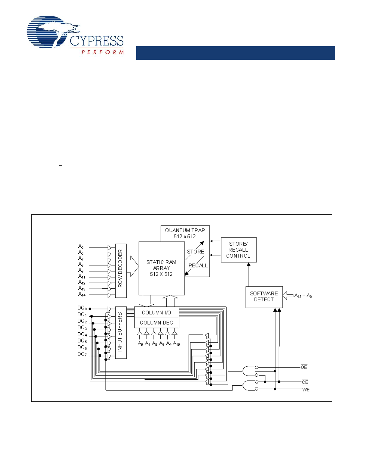
Logic Block Diagram
■
25 ns and 45 ns access times
■
Pin compatible with industry standard SRAMs
■
Software initiated STORE and RECALL
■
Automatic RECALL to SRAM on power up
■
Unlimited Read and Write endurance
■
Unlimited RECALL cycles
■
1,000,000 STORE cycles
■
100 year data retention
■
Single 5V+10% power supply
■
Commercial and Industrial Temperatures
■
28-pin (300 mil and 330 mil) SOIC packages
■
RoHS compliance
Functional Description
The Cypress STK11C88 is a 256 Kb fast static RAM with a
nonvolatile element in each memory cell. The embedded
nonvolatile elements incorporate QuantumTrap
producing the world’s most reliable nonvolatile memory. The
SRAM provides unlimited read and write cycles, while
independent, nonvolatile data resides in the highly reliable
QuantumTrap cell. Data transfers under Software control from
SRAM to the nonvolatile elements (the STORE operation). On
power up, data is automatically restored to the SRAM (the
RECALL operation) from the nonvolatile memory. RECALL
operations are also available under software control.
™
technology
Cypress Semiconductor Corporation • 198 Champion Court • San Jose,CA 95134-1709 • 408-943-2600
Document Number: 001-50591 Rev. ** Revised January 29, 2009
[+] Feedback

STK11C88
Pin Configurations
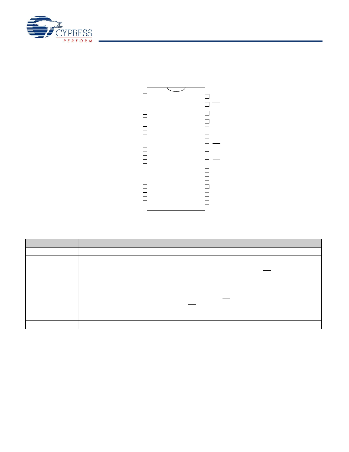
Figure 1. Pin Diagram - 28-Pin SOIC
$
$
'4
'4
'4
9
$
$
$
$
$
$
$
$
66
723
9
:(
$
$
$
$
2(
$
&(
'4
'4
'4
'4
'4
&&
Table 1. Pin Definitions - 28-Pin SOIC
Pin Name Alt IO Type Description
A
0–A14
DQ
-DQ
0
7
WE W
CE
OE
V
SS
V
CC
E
G
Input Address Inputs. Used to select one of the 32,768 bytes of the nvSRAM.
Input or
Bidirectional Data IO lines. Used as input or output lines depending on operation.
Output
Input Write Enable Input, Active LOW. When the chip is enabled and WE is LOW, data on the
IO pins is written to the specific address location.
Input Chip Enable Input, Active LOW. W hen LOW, selects th e chip. When H IGH, desel ects the
chip.
Input Output Enable, Active LOW. The active LOW OE input enables the data output buffers
during read cycles. Deasserting OE
HIGH causes the IO pins to tri-state.
Ground Ground for the Device. The device is connected to the ground of the system.
Power Supply Power Supply Inputs to the Device.
Document Number: 001-50591 Rev. ** Page 2 of 15
[+] Feedback

STK11C88
Device Operation
The STK11C88 is a versatile memory chip that provides several
modes of operation. The STK11C88 can operate as a standard
32K x 8 SRAM. A 32K x 8 array of nonvolatile storage elements
shadow the SRAM. SRAM data can be copied from nonvolatile
memory or nonvolatile data can be recalled to the SRAM.
SRAM Read
The STK11C88 performs a READ cycle whenever CE and OE
are LOW, while WE is HIGH. The address specified on pins
A
determines the 32,768 data bytes accessed. When the
0–14
READ is initiated by an address transition, the outputs are valid
after a delay of t
CE
or OE, the outputs are valid at t
later (READ cycle 2). The data outputs repeatedly respond to
address changes within the t
transitions on any control input pins, and remain valid until
another address change or until CE
(READ cycle 1). If the READ is initiated by
AA
access time without the need for
AA
ACE
or at t
, whichever is
DOE
or OE is brought HIGH.
SRAM Write
A WRITE cycle is performed whenever CE and WE are LOW.
The address inputs must be stable prior to entering the WRITE
cycle and must remain stable until either CE or WE goes HIGH
at the end of the cycle. The data on the common IO pins DQ
are written into the memory if it has valid tSD, before the end of
controlled WRITE or before the end of an CE controlled
a WE
WRITE. Keep OE
data bus contention on common IO lines. If OE
internal circuitry turns off the ou tput buff ers t
LOW.
HIGH during the entire WRITE cycle to avoid
is left LOW,
after WE goes
HZWE
0–7
Software ST ORE
Data is transferred from the SRAM to the nonvolatile memory by
a software address sequence. The STK11C88 software ST ORE
cycle is initiated by executing sequential CE
cycles from six specific address locations in exact order. During
the STORE cycle, an erase of the previous nonvolatile data is
first performed, followed by a program of the nonvolatile
elements. When a STORE cycle is initiated, input and output are
disabled until the cycle is completed.
Because a sequence of READs from specific addresses is used
for STORE initiation, it is important that no other READ or WRITE
accesses intervene in the sequence. If they intervene, the
sequence is aborted and no STORE or RECALL takes place.
To initiate the software STORE cycle, the following READ
sequence is performed:
controlled READ
1. Read address 0x0E38, Valid READ
2. Read address 0x31C7, Valid READ
3. Read address 0x03E0, Valid READ
4. Read address 0x3C1F, Valid READ
5. Read address 0x303F, Valid READ
6. Read address 0x0FC0, Initiate STORE cycle
The software sequence is clocked with CE
controlled READs.
When the sixth address in the sequence is entered, the STORE
cycle commences and the chip is disabled. It is important that
READ cycles and not WRITE cycles are used in the seque nce.
It is not necessary that OE is LOW for a valid sequence. After the
t
cycle time is fulfilled, the SRAM is again activated for
STORE
READ and WRITE operation.
Software RECALL
Data is transferred from the nonvolatile memory to the SRAM by
a software address sequence. A software RECALL cycle is
initiated with a sequence of READ operations in a manner similar
to the software STORE initiation. To initiate the RECALL cycle,
the following sequence of CE controlled READ operations is
performed:
1. Read address 0x0E38, Valid READ
2. Read address 0x31C7, Valid READ
3. Read address 0x03E0, Valid READ
4. Read address 0x3C1F, Valid READ
5. Read address 0x303F, Valid READ
6. Read address 0x0C63, Initiate RECALL cycle
Internally, RECALL is a two step procedure. First, the SRAM data
is cleared, and then the nonvolatile information is transferred into
the SRAM cells. After the t
again ready for READ and WRITE operations. The RECALL
cycle time, the SRAM is once
RECALL
operation does not alter the data in the nonvolatile elements. The
nonvolatile data can be recalled an unlimited number of times.
Hardware RECALL (Power Up)
During power up or after any low power condition (VCC<V
an internal RECALL request is latched. When V
exceeds the sense voltage of V
automatically initiated and takes t
If the STK11C88 is in a WRITE
RECALL, the SRAM
data is corrupted. To help avoid this
HRECALL
state at the end of power up
, a RECALL cycle is
SWITCH
to complete.
situation, a 10 Kohm resistor is connected either be tween WE
and system VCC or between CE and system VCC.
RESET
once again
CC
),
Document Number: 001-50591 Rev. ** Page 3 of 15
[+] Feedback

STK11C88
Hardware Protect
The STK11C88 of fers hardware protection against inadvertent
STORE operation and SRAM WRITEs during low voltage
conditions. When VCC<V
STORE operations and SRAM WRITEs are inhibited.
, all externally initiated
SWITCH
Noise Considerations
The STK11C88 is a high speed memory. It must have a high
frequency bypass capacitor of approximately 0.1 µF
connected between VCC and V
are as short as possible. As with all high speed CMOS ICs,
careful routing of power, ground, and signals help prevent
noise problems.
using leads and traces that
SS,
Low Average Active Power
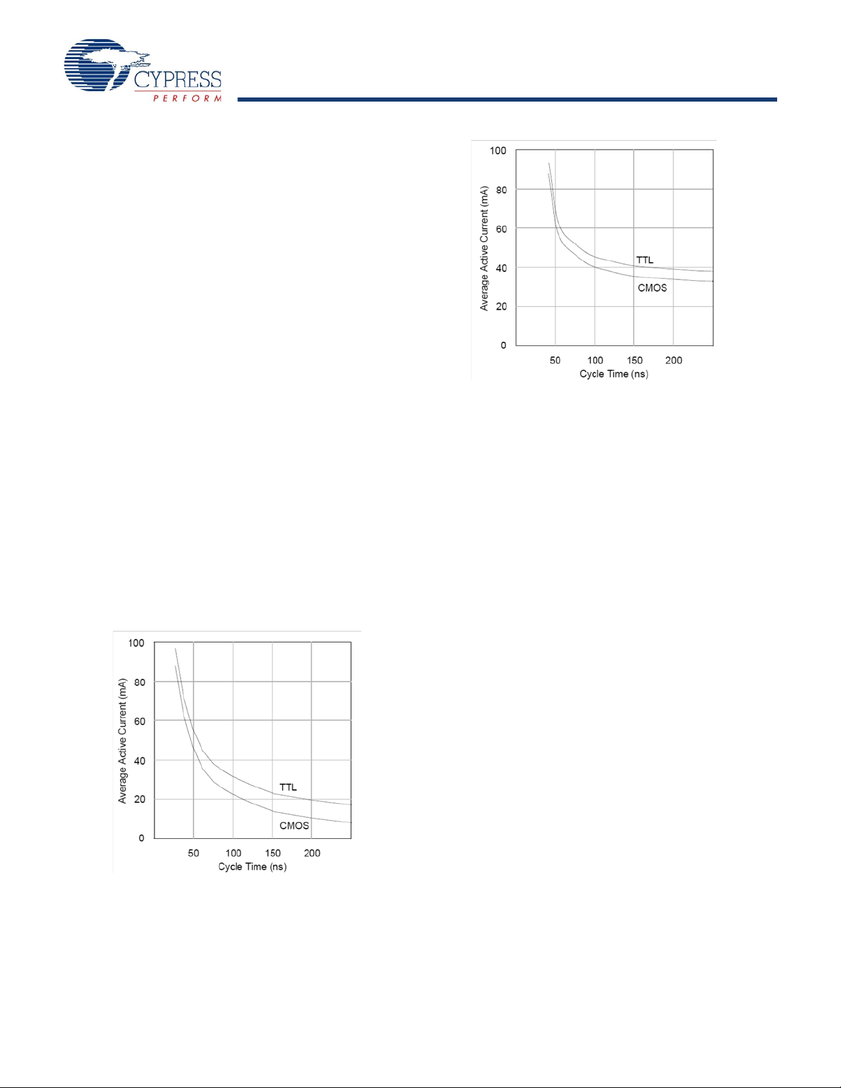
CMOS technology provides the STK11C88 the benefit of
drawing significantly less current when it is cycled at times
longer than 50 ns. Figure 2 and Figure 3 show the relationship
between I
current consumption is shown for both CMOS and TTL input
levels (commercial temperature range, VCC = 5.5V, 100
percent duty cycle on chip enable). Only standby current is
drawn when the chip is disabled. The overall average current
drawn by the STK11C88 depends on the following items:
1. The duty cycle of chip enable
2. The overall cycle rate for accesses
3. The ratio of READs to WRITEs
4. CMOS versus TTL input levels
5. The operating temperature
6. The V
7. IO loading
Figure 2. Icc (max) Reads
and READ or WRITE cycle time. Worst case
CC
level
CC
Figure 3. Icc (max) Writes
Best Practices
nvSRAM products have been used effectively for over 15
years. While ease-of-use is one of the product’s main system
values, the experience gained working with hundreds of applications has resulted in the following suggestions as best
practices:
■
The nonvolatile cells in a nvSRAM are programmed on the
test floor during final test and quality assurance. Incoming
inspection routines at customer or contract manufacturer’s
sites, sometimes, reprogram these values. Final NV patterns
are typically repeating patterns of AA, 55, 00, FF, A5, or 5A.
The end product’s firmware should not assume that a NV
array is in a set programmed state. Routines that check
memory content values to determine first time system configuration and cold or warm boot status, should always program
a unique NV pattern (for example, a complex 4-byte pattern
of 46 E6 49 53 hex or more random bytes) as part of the final
system manufacturing test to ensure these system routines
work consistently.
■
Power up boot firmware routines should rewrite the nvSRAM
into the desired state. While the nvSRAM is shipped in a
preset state, best practice is to again rewrite the nvSRAM
into the desired state as a safeguard against events that
might flip the bit inadvertently (program bugs or incoming
inspection routines).
Document Number: 001-50591 Rev. ** Page 4 of 15
[+] Feedback

STK11C88
Table 2. Software STORE/RECALL Mode Selection
Notes
1. The six consecutive addresses must be in the order listed. WE
must be high during all six consecutive CE controlled cycles to enable a nonvolatile cycle.
2. While there are 15 addresses on the STK11C88, only the lower 14 are used to control software modes.
CE WE
A13 – A
L H 0x0E38
0x31C7
0x03E0
0x3C1F
0x303F
0x0FC0
L H 0x0E38
0x31C7
0x03E0
0x3C1F
0x303F
0x0C63
0
Mode IO Notes
Read SRAM
Read SRAM
Read SRAM
Read SRAM
Read SRAM
Nonvolatile STORE
Read SRAM
Read SRAM
Read SRAM
Read SRAM
Read SRAM
Nonvolatile RECALL
Output Data
Output Data
Output Data
Output Data
Output Data
Output Data
Output Data
Output Data
Output Data
Output Data
Output Data
Output Data
[1, 2]
[1, 2]
Document Number: 001-50591 Rev. ** Page 5 of 15
[+] Feedback
 Loading...