Cypress STK11C68-5 User Manual

STK11C68-5 (SMD5962-92324)
64 Kbit (8K x 8) SoftStore nvSRAM
Features
STORE/
RECALL
CONTROL
POWER
CONTROL
SOFTWARE
DETECT
STATIC RAM
ARRAY
128 X 512
Quantum Trap
128 X 512
STORE
RECALL
COLUMN I/O
COLUMN DEC
ROW DECODER
INPUT BUFFERS
OE
CE
WE
HSB
V
CC
V
CAP
A
0
- A
12
A
0
A
1
A
2
A
3
A
4
A
10
A
5
A
6
A
7
A
8
A
9
A
11
A
12
DQ
0
DQ
1
DQ
2
DQ
3
DQ
4
DQ
5
DQ
6
DQ
7
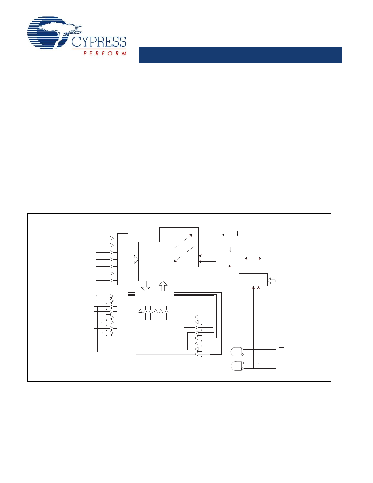
Logic Block Diagram
Functional Description
■ 35 ns, 45 ns, and 55 ns access times
■ Pin compatible with industry standard SRAMs
■ Software initiated nonvolatile STORE
■ Unlimited Read and Write endurance
■ Automatic RECALL to SRAM on power up
■ Unlimited RECALL cycles
■ 1,000,000 STORE cycles
■ 100 year data retention
■ Single 5V ± 10% operation
■ Military temperature
■ 28-pin (300 mil) CDIP and 28-pad LCC packages
The Cypress STK11C68-5 is a 64 Kb fast static RAM with a
nonvolatile element in each memory cell. The embedded
nonvolatile elements incorporate QuantumTrap technology to
produce the world’s most reliable nonvolatile memory. The
SRAM provides unlimited read and write cycles, while
independent nonvolatile data resides in the highly reliable
QuantumTrap cell. Data transfers under software control from
SRAM to the nonvolatile elements (the STORE operation). On
power up, data is automatically restored to the SRAM (the
RECALL operation) from the nonvolatile memory. RECALL
operations are also available under software control.
Cypress Semiconductor Corporation • 198 Champion Court • San Jose, CA 95134-1709 • 408-943-2600
Document Number: 001-51001 Rev. *A Revised April 07, 2009
[+] Feedback

STK11C68-5 (SMD5962-92324)
Pinouts
1&
$
$
$
$
$
$
$
$
'4
'4
'4
9
66
9
&&
1&
$
$
$
$
'4
'4
'4
'4
'4
$
:(
2(
&(
723
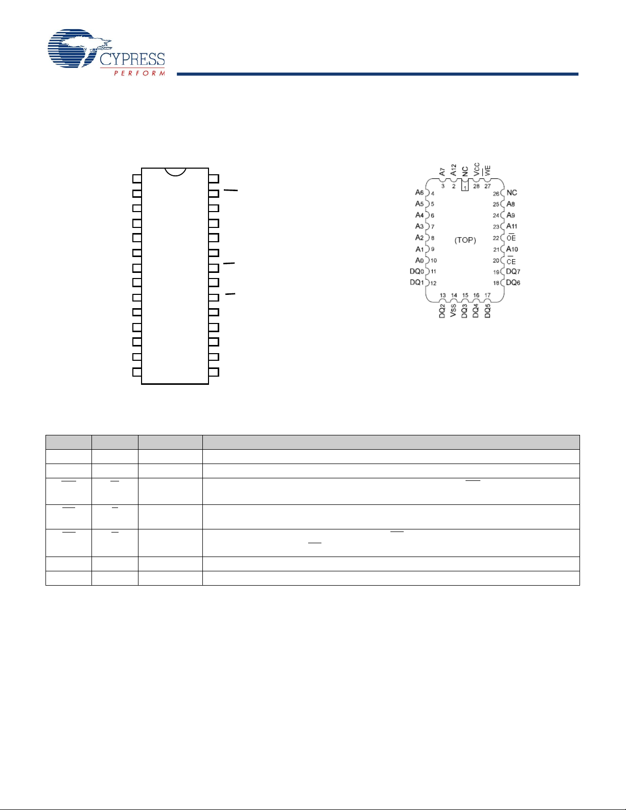
Figure 1. Pin Diagram - 28-Pin DIP
Figure 2. Pin Diagram - 28-Pin LLC
Pin Definitions
Pin Name Alt I/O Type Description
A
0–A12
DQ
-DQ
0
7
WE
CE
OE
V
SS
V
CC
Document Number: 001-51001 Rev. *A Page 2 of 15
W
E
G
Input/Output Bidirectional Data I/O Lines. Used as input or output lines depending on operation.
Power Supply Power Supply Inputs to the Device.
Input Addre ss Inputs. Used to select one of the 8,192 bytes of the nvSRAM.
Input
Write Enable Input, Active LOW . When the chip is enabled and WE is LOW, dat a on the I/O
pins is written to the specific address location.
Input Chip Enable Input, Active LOW. When LOW, selects the chip. When HIGH, deselects the
chip.
Input
Output Enable, Active LOW. The active LOW OE input enables the data output buffers during
read cycles. Deasserting OE
HIGH causes the I/O pins to tristate.
Ground Ground for the Device. The device is connected to ground of the system.
[+] Feedback

STK11C68-5 (SMD5962-92324)
Device Operation
The STK11C68-5 is a versatile memory chip that provides
several modes of operation. The STK11C68-5 can operate as a
standard 8K x 8 SRAM. It has an 8K x 8 Nonvolatile Elements
shadow to which the SRAM information can be copied or fro m
which the SRAM can be updated in nonvolatile mode.
The software sequence is clocked with CE
controlled Reads.
When the sixth address in the sequence is entered, the STORE
cycle commences and the chip is disabled. It is important that
Read cycles and not Write cycles are used in the sequence. It is
not necessary that OE is LOW for a valid sequence. After the
t
cycle time is fulfilled, the SRAM is again activated for
STORE
Read and Write operation.
SRAM Read
The STK11C68-5 performs a Read cycle whenever CE and OE
are LOW while WE is HIGH. The address specified on pins A
0–12
determines the 8,192 data bytes accessed. When the Read is
initiated by an address transition, the outputs are valid after a
delay of t
the outputs are valid at t
(Read cycle 1). If the Read is initiated by CE or OE,
AA
ACE
or at t
, whichever is later (Read
DOE
cycle 2). The data outputs repeatedly respond to address
changes within the t
access time without the need for
AA
transitions on any control input pins. They remain valid until
another address change or until CE
or OE is brought HIGH, or
WE is brought LOW.
SRAM Write
A Write cycle is performed whenever CE and WE are LOW . Th e
address inputs must be stable before entering the Write cycle
and must remain stable until either CE or WE goes HIGH at the
end of the cycle. The data on the common I/O pins DQ
written into the memory if it has valid t
end of a WE
controlled Write or before the end of an CE
. This is done before the
SD
0–7
are
controlled Write. Keep OE HIGH during the entire Write cycle to
avoid data bus contention on common I/O lines. If OE
internal circuitry turns off the output buffers t
LOW.
HZWE
is left LOW,
after WE goes
Software ST OR E
Data is transferred from the SRAM to the nonvolatile memory by
a software address sequence. The STK11C68-5 software
STORE cycle is initiated by executing sequential CE controlled
Read cycles from six specific address locations in exact order.
During the STORE cycle, an erase of the previous nonvolatile
data is first performed followed by a program of the nonvolatile
elements. When a STORE cycle is initiated, input and output are
disabled until the cycle is completed.
Because a sequence of Reads from specific addresses is used
for STORE initiation, it is important that no other Read or Write
accesses intervene in the sequence. If they intervene, the
sequence is aborted and no STORE or RECALL takes place.
To initiate the software STORE cycle, the following Read
sequence is performed:
1. Read address 0x0000, Valid READ
2. Read address 0x1555, Valid READ
3. Read address 0x0AAA, Valid READ
4. Read address 0x1FFF, Valid READ
5. Read address 0x10F0, Valid READ
6. Read address 0x0F0F, Initiate STORE cycle
Software RECALL
Data is transferred from the nonvolatile memory to the SRAM by
a software address sequence. A software RECALL cycle is
initiated with a sequence of Read operations in a manner similar
to the software STORE initiation. To initiate the RECALL cycle,
the following sequence of CE
controlled Read operations is
performed:
1. Read address 0x0000, Valid READ
2. Read address 0x1555, Valid READ
3. Read address 0x0AAA, Valid READ
4. Read address 0x1FFF, Valid READ
5. Read address 0x10F0, Valid READ
6. Read address 0x0F0E, Initiate RECALL cycle
Internally, RECALL is a two step procedure. First, the SRAM data
is cleared; then, the nonvolatile information is transferred into the
SRAM cells. After the t
ready for Read and Write operations. The RECALL operation
cycle time, the SRAM is again
RECALL
does not alter the data in the nonvolatile elements. The
nonvolatile data can be recalled an unlimited number of times.
Hardware RECALL (Power Up)
During power up or after any low power condition (VCC <
V
), an internal RECALL request is latched. When V
RESET
once again exceeds the sense voltage of V
cycle is automatically initiated and takes t
If the STK11C68-5 is in a Write
RECALL, the SRAM
data is corrupted. To help avoid this
state at the end of power up
HRECALL
SWITCH
, a RECALL
to complete.
CC
situation, a 10 Kohm resistor is connected either be tween WE
and system VCC or between CE and system VCC.
Hardware Protect
The STK11C68-5 of fers hardware protection against inadvertent
STORE operation and SRAM Writes during low voltage
conditions. When V
operations and SRAM Writes are inhibited.
CAP
< V
, all externally initiated STORE
SWITCH
Noise Considerations
The STK11C68-5 is a high speed memory. It must have a high
frequency bypass capacitor of approximately 0.1 µF connected
between V
as possible. As with all high speed CMOS ICs, careful routing of
power, ground, and signals reduce circuit noise.
CC
and V
using leads and traces that are as short
SS,
Document Number: 001-51001 Rev. *A Page 3 of 15
[+] Feedback

STK11C68-5 (SMD5962-92324)
Low Average Active Power
Note
1. The six consecutive addresses must be in the order listed. WE
must be high during all six consecutive CE controlled cycles to enable a nonvolatile cycle.
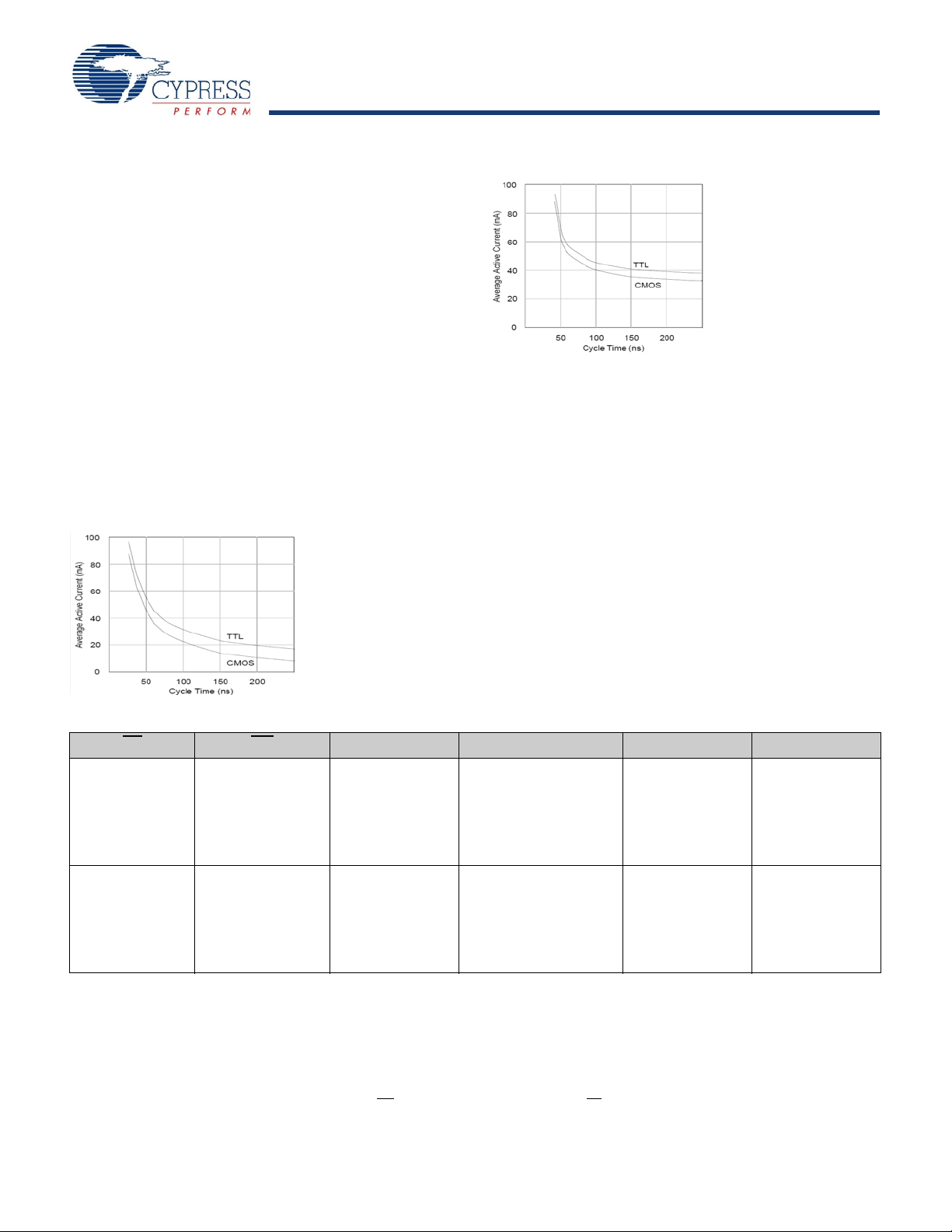
CMOS technology provides the STK11C68-5 the benefit of
drawing significantly less current when it is cycled at times longer
than 50 ns. Figure 3 and Figure 4 shows the relationship
between I
consumption is shown for both CMOS and TTL input levels
(commercial temperature range, VCC = 5.5V, 100% duty cycle
on chip enable). Only standby current is drawn when the chip is
disabled. The overall average current drawn by the STK11C68-5
depends on the following items:
■ Duty cycle of chip enable
■ Overall cycle rate for accesses
■ Ratio of Reads to Writes
■ CMOS versus TTL input levels
■ Operating temperature
■ V
CC
■ I/O loading
Figure 3. Current Versus Cy c le Time (Read)
and Read or Write cycle time. Worst case current
CC
level
Figure 4. Current Versus Cycle Time (Write)
Best Practices
Cypress nvSRAM products have been used effectively for over
15 years. While ease of use is one of the product’s main system
values, the experience gained from working with hundreds of
applications has resulted in the following suggestions as best
practices:
■ The nonvolatile cells in an nvSRAM are programmed on the
test floor during final test and quality assurance. Incoming
inspection routines at customer or contract manufacturer’s
sites sometimes reprograms these values. Final NV patterns
are typically repeating patterns of AA, 55, 00, FF, A5, or 5A.
The end product’s firmware must not assume that an NV array
is in a set programmed state. Routines that check memory
content values to determine first time system configuration.
■ Cold or warm boot status, and so on must always program a
unique NV pattern (for example, complex 4-byte pattern of 46
E6 49 53 hex or more random bytes) as part of the final system
manufacturing test. This is to ensure these system routines
work consistently.
Table 1. Hardware Mode Selection
CE WE A12–A0 Mode I/O Notes
L H 0x0000
0x1555
0x0AAA
0x1FFF
0x10F0
0x0F0F
L H 0x0000
0x1555
0x0AAA
0x1FFF
0x10F0
0x0F0E
Read SRAM
Read SRAM
Read SRAM
Read SRAM
Read SRAM
Nonvolatile STORE
Read SRAM
Read SRAM
Read SRAM
Read SRAM
Read SRAM
Nonvolatile RECALL
Output Data
Output Data
Output Data
Output Data
Output Data
Output High Z
Output Data
Output Data
Output Data
Output Data
Output Data
Output High Z
[1]
[1]
Document Number: 001-51001 Rev. *A Page 4 of 15
[+] Feedback

STK11C68-5 (SMD5962-92324)
Maximum Ratings
Note
2. CE
> VIH does not produce standby current levels until any nonvolatile cycle in progress has timed out.
3. These parameters are guaranteed by design and are not tested.
Exceeding maximum ratings may shorten the useful life of the
device. These user guidelines are not tested.
Storage Tem perature ................................. –65°C to +150°C
Voltage on DQ
Power Dissipation .........................................................1.0W
DC Output Current (1 output at a time, 1s duration).... 15 mA
Operating Range
...................................–0.5V to Vcc + 0.5V
0-7
Temperature under bias..............................–55°C to +125°C
Supply Voltage on VCC Relative to GND..........–0.5V to 7.0V
Voltage on Input Relative to Vss............–0.6V to V
+ 0.5V
CC
Range
Military -55°C to +125°C 4.5V to 5.5V
Ambient
Temperature
V
CC
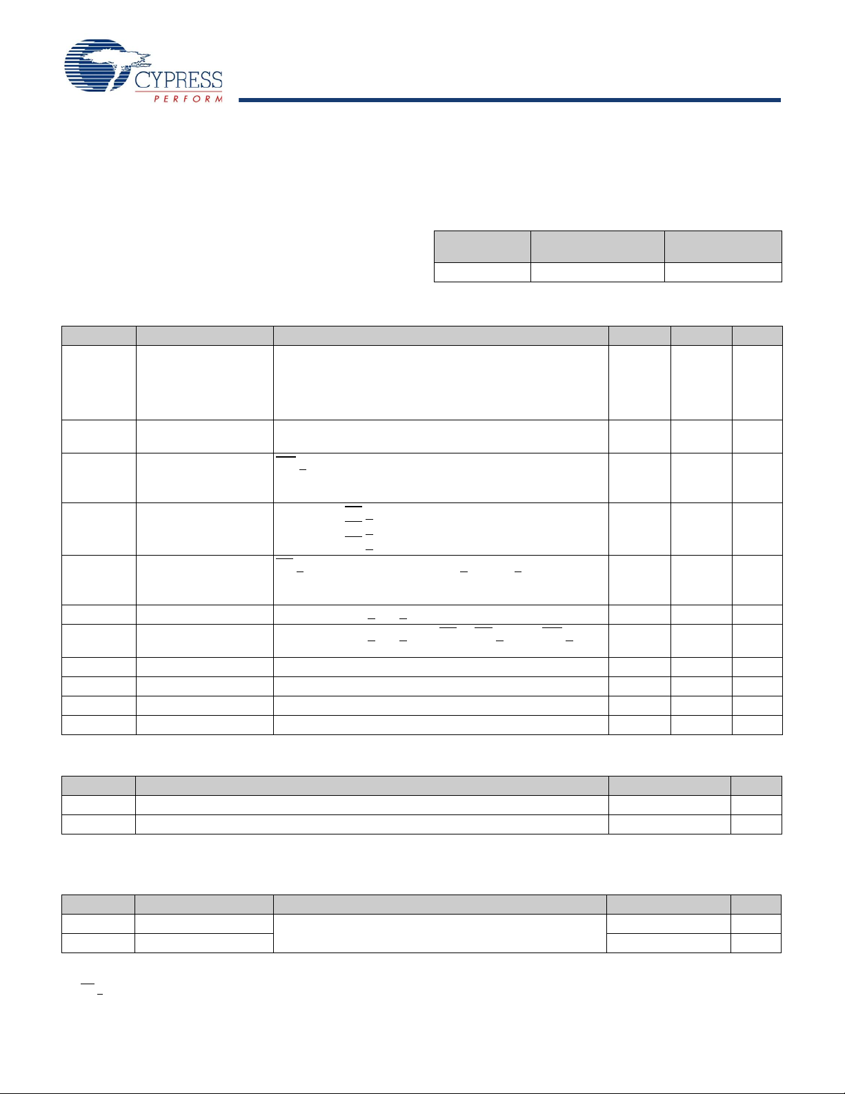
DC Electrical Characteristics
Over the operating range (VCC = 4.5V to 5.5V)
Parameter Description Test Conditions Min Max Unit
I
CC1
I
CC2
I
CC3
I
SB1
I
SB2
I
IX
I
OZ
V
V
V
V
IH
IL
OH
OL
Average VCC Current tRC = 35 ns
t
= 45 ns
RC
t
= 55 ns
RC
Dependent on output loading and cycle rate. Values obtained
without output loads. I
Average VCC Current
during STORE
Average VCC Current at
t
= 200 ns, 5V, 25°C
RC
Typical
[2]
VCC Standby Current
(Standby, Cycling TTL
Input Levels)
[2]
VCC Standby Current
All Inputs Do Not Care, VCC = Max
Average current for duration t
WE
> (VCC – 0.2V). All other inputs cycling.
Dependent on output loading and cycle rate. Values obtained
without output loads.
t
= 35 ns, CE > V
RC
tRC = 45 ns, CE > V
tRC = 55 ns, CE > V
CE > (VCC – 0.2V). All others V
Standby current level after nonvolatile cycle is complete.
IH
IH
IH
OUT
= 0 mA
STORE
IN
< 0.2V or > (VCC – 0.2V).
Inputs are static. f = 0 MHz
Input Leakage Current VCC = Max, VSS < V
Off State Output
VCC = Max, VSS < V
Leakage Current
< V
IN
CC
< VCC, CE or OE > V
IN
or WE < V
IH
-1 +1 μA
IL
-5 +5 μA
Input HIGH Voltage 2.2 VCC + 0.5 V
Input LOW Voltage VSS – 0.5 0.8 V
Output HIGH Voltage I
Output LOW Voltage I
= –4 mA 2.4 V
OUT
= 8 mA 0.4 V
OUT
75
65
55
3mA
10 mA
24
21
20
1500 μA
mA
mA
mA
mA
mA
mA
Data Retention and Endurance
Parameter Description Min Unit
DATA
NV
C
R
Data Retention 100 Years
Nonvolatile STORE Operations 1,000 K
Capacitance
In this table, the capacitance parameters are listed.
Parameter Description Test Conditions Max Unit
C
C
IN
OUT
Input Capacitance TA = 25°C, f = 1 MHz,
V
= 0 to 3.0V
Output Capacitance 7pF
CC
Document Number: 001-51001 Rev. *A Page 5 of 15
[3]
8pF
[+] Feedback
 Loading...