

Page 1
STK11C68
64 Kbit (8K x 8) SoftStore nvSRAM
Features
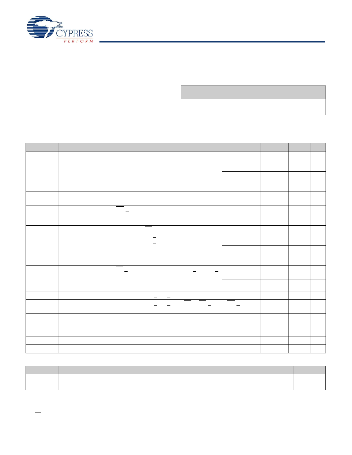
STORE/
RECALL
CONTROL
POWER
CONTROL
SOFTWARE
DETECT
STATIC RAM
ARRAY
128 X 512
Quantum Trap
128 X 512
STORE
RECALL
COLUMN I/O
COLUMN DEC
ROW DECODER
INPUT BUFFERS
OE
CE
WE
HSB
V
CC
V
CAP
A
0
-
A
12
A
0
A
1
A
2
A
3
A
4
A
10
A
5
A
6
A
7
A
8
A
9
A
11
A
12
DQ
0
DQ
1
DQ
2
DQ
3
DQ
4
DQ
5
DQ
6
DQ
7
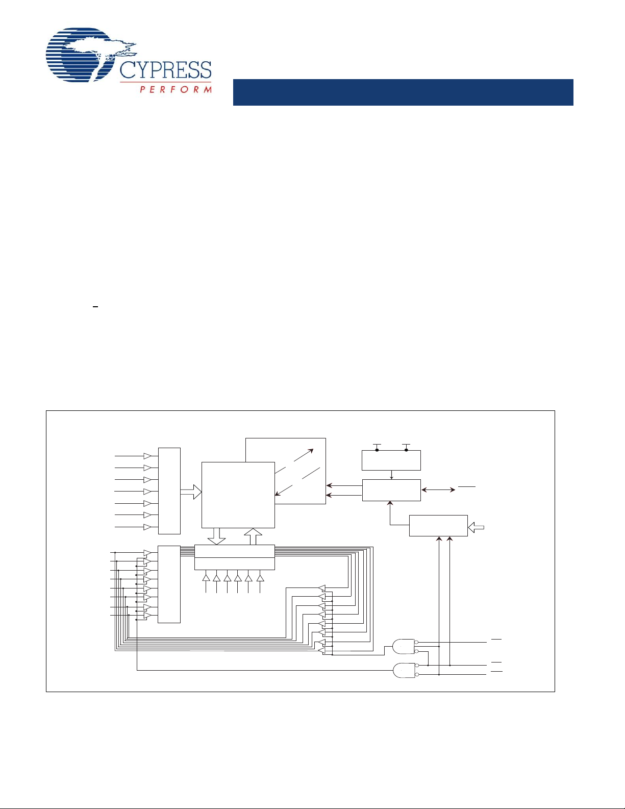
Logic Block Diagram
■
25 ns, 35 ns, and 45 ns access times
■
Pin compatible with industry standard SRAMs
■
Software initiated nonvolatile STORE
■
Unlimited Read and Write endurance
■
Automatic RECALL to SRAM on power up
■
Unlimited RECALL cycles
■
1,000,000 STORE cycles
■
100 year data retention
■
Single 5V+10% operation
■
Commercial and industrial temperature
■
28-pin (330 mil) SOIC package
■
28-pin (300 mil) CDIP and 28-pad (350 mil) LCC packages
■
RoHS compliance
Functional Description
The Cypress STK11C68 is a 64Kb fast st atic RAM with a nonvolatile element in each memory cell. The embedded nonvolatile
elements incorporate QuantumTrap technology producing the
world’s most reliable nonvolatile memory. The SRAM provides
unlimited read and write cycles, while independent n onvolatile
data resides in the highly reliable QuantumTrap cell. Data
transfers under software control from SRAM to the nonvolatile
elements (the STORE operation). On power up, data is automatically restored to the SRAM (the RECALL operation) from the
nonvolatile memory. RECALL operations are also available
under software control.
Cypress Semiconductor Corporation • 198 Champion Court • San Jose,CA 95134-1709 • 408-943-2600
Document Number: 001-50638 Rev. ** Revised January 30, 2009
[+] Feedback
Page 2
STK11C68
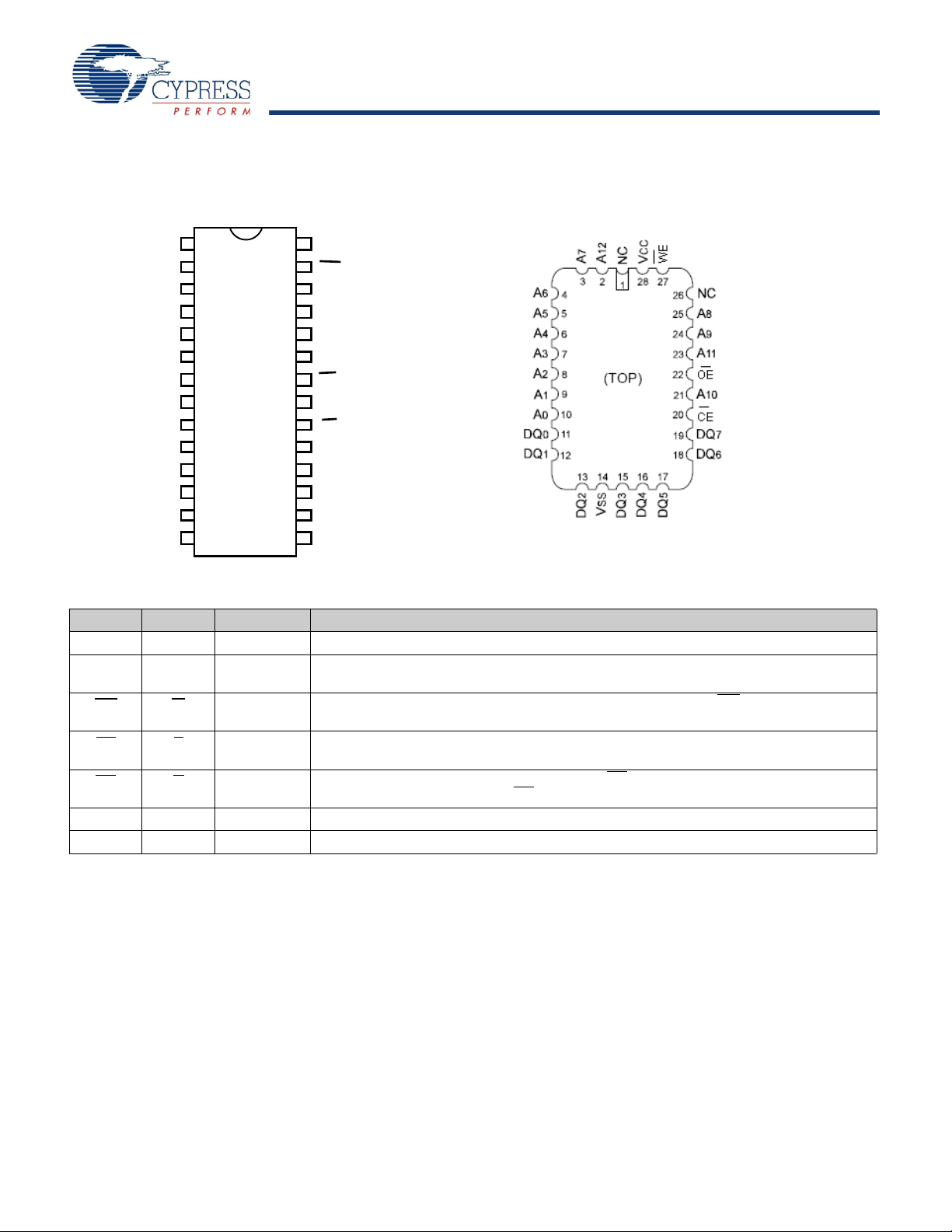
Pin Configurations
1&
$
$
$
$
$
$
$
$
'4
'4
'4
9
66
9
&&
1&
$
$
$
$
'4
'4
'4
'4
'4
$
:(
2(
&(
723
Pin Definitions
Figure 1. Pin Diagram - 28-Pin SOIC/DIP and 28-Pin LLC
Pin Name Alt IO Type Description
A
0–A12
DQ
-DQ
0
7
WE
W
CE E
OE
V
SS
V
CC
Document Number: 001-50638 Rev. ** Page 2 of 16
G
Input Address Inputs. Used to select one of the 8,192 bytes of the nvSRAM.
Input or
Bidirectional Data IO Lines. Used as input or output lines depending on operation.
Output
Input Write Enable Input, Active LOW. When the chip is enabled and WE is LOW, data on the
IO pins is written to the specific address location.
Input Chip Enable Input, Active LOW. W hen LOW, selects th e chip. When H IGH, desel ects the
chip.
Input Output Enable, Active LOW. The active LOW OE input enables the data output buffers
during read cycles. Deasserting OE
HIGH causes the IO pins to tri-state.
Ground Ground for the Device. The device is connected to ground of the system.
Power Supply Power Supply Inputs to the Device.
[+] Feedback
Page 3
STK11C68
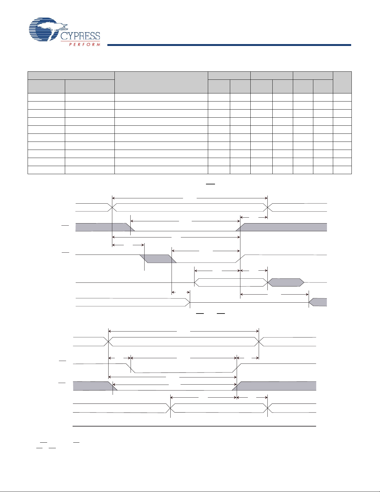
Device Operation
The STK11C68 is a versatile memory chip that provides several
modes of operation. The STK16C88 can operate as a standard
8K x 8 SRAM. A 8K x 8 array of nonvolatile storage ele ments
shadow the SRAM. SRAM data can be copied nonvolatile
memory or nonvolatile data can be recalled to the SRAM.
SRAM Read
The STK11C68 performs a Read cycle whenever CE and OE are
LOW while WE
determines the 8,192 data bytes accessed. When the Read is
initiated by an address transition, the outputs are valid after a
delay of t
the outputs are valid at t
cycle 2). The data outputs repeatedly respond to address
changes within the t
tions on any control input pins, and remains valid until a nother
address change or until CE
brought LOW.
is HIGH. The address specified on pins A
(Read cycle 1). If the Read is initiated by CE or OE,
AA
or at t
ACE
access time without the need for transi-
AA
, whichever is later (Read
DOE
or OE is brought HIGH, or WE
0–12
SRAM Write
A Write cycle is performed whenever CE and WE are LOW . Th e
address inputs must be stable prior to entering the Write cycle
and must remain stable until either CE
end of the cycle. The data on the common IO pins DQ
written into the memory if it has valid t
controlled Write or before the end of an CE controlled Write.
Keep OE
HIGH during the entire Write cycle to avoid data bus
contention on common IO lines. If OE
circuitry turns off the output buffers t
or WE goes HIGH at the
, before the end of a WE
SD
0–7
is left LOW, internal
after WE goes LOW.
HZWE
are
Software ST ORE
Data is transferred from the SRAM to the nonvolatile memory by
a software address sequence. The STK11C68 software ST ORE
cycle is initiated by executing sequential CE controlled Read
cycles from six specific address locations in exact order. During
the STORE cycle, an erase of the previous nonvolatile data is
first performed followed by a program of the nonvolatile
elements. When a STORE cycle is initiated, input and output are
disabled until the cycle is completed.
Because a sequence of Reads from specific addresses is used
for STORE initiation, it is important that no other Read or Write
accesses intervene in the sequence. If they intervene, the
sequence is aborted and no STORE or RECALL takes place.
To initiate the software STORE cycle, the following Read
sequence is performed:
1. Read address 0x0000, Valid READ
2. Read address 0x1555, Valid READ
3. Read address 0x0AAA, Valid READ
4. Read address 0x1FFF, Valid READ
5. Read address 0x10F0, Valid READ
6. Read address 0x0F0F, Initiate STORE cycle
The software sequence is clocked with CE
When the sixth address in the sequence is entered, the STORE
cycle commences and the chip is disabled. It is important that
Read cycles and not Write cycles are used in the sequence. It is
controlled Reads.
not necessary that OE
cycle time is fulfilled, the SRAM is again activated for
t
STORE
Read and Write operation.
is LOW for a valid sequence. After the
Software RECALL
Data is transferred from the nonvolatile memory to the SRAM by
a software address sequence. A software RECALL cycle is
initiated with a sequence of Read operations in a manner similar
to the software STORE initiation. To initiate the RECALL cycle,
the following sequence of CE
controlled Read operations is
performed:
1. Read address 0x0000, Valid READ
2. Read address 0x1555, Valid READ
3. Read address 0x0AAA, Valid READ
4. Read address 0x1FFF, Valid READ
5. Read address 0x10F0, Valid READ
6. Read address 0x0F0E, Initiate RECALL cycle
Internally, RECALL is a two step procedure. First, the SRAM data
is cleared; then, the nonvolatile information is transferred into the
SRAM cells. After the t
ready for Read and Write operations. The RECALL operation
cycle time, the SRAM is again
RECALL
does not alter the data in the nonvolatile elements. The nonvolatile data can be recalled an unlimited number of times.
Hardware RECALL (Power Up)
During power up or after any low power condition (VCC <
V
once again exceeds the sense voltage of V
cycle is automatically initiated and takes t
), an internal RECALL request is latched. When V
RESET
SWITCH
HRECALL
, a RECALL
to complete.
CC
If the STK11C68 is in a Write state at the end of power up
RECALL, the SRAM
data is corrupted. To help avoid this
situation, a 10 Kohm resistor is connected either be tween WE
and system VCC or between CE and system VCC.
Hardware Protect
The STK11C68 offers hardware protection against inadvertent
STORE operation and SRAM Writes during low voltage conditions. When V
operations and SRAM Writes are inhibited.
CAP<VSWITCH
, all externally initiated STORE
Noise Considerations
The STK11C68 is a high speed memory. It must have a high
frequency bypass capacitor of approximately 0.1 µF connected
between V
as possible. As with all high speed CMOS ICs, careful routing of
CC
and V
using leads and traces that are as short
SS,
power, ground, and signals reduce circuit noise.
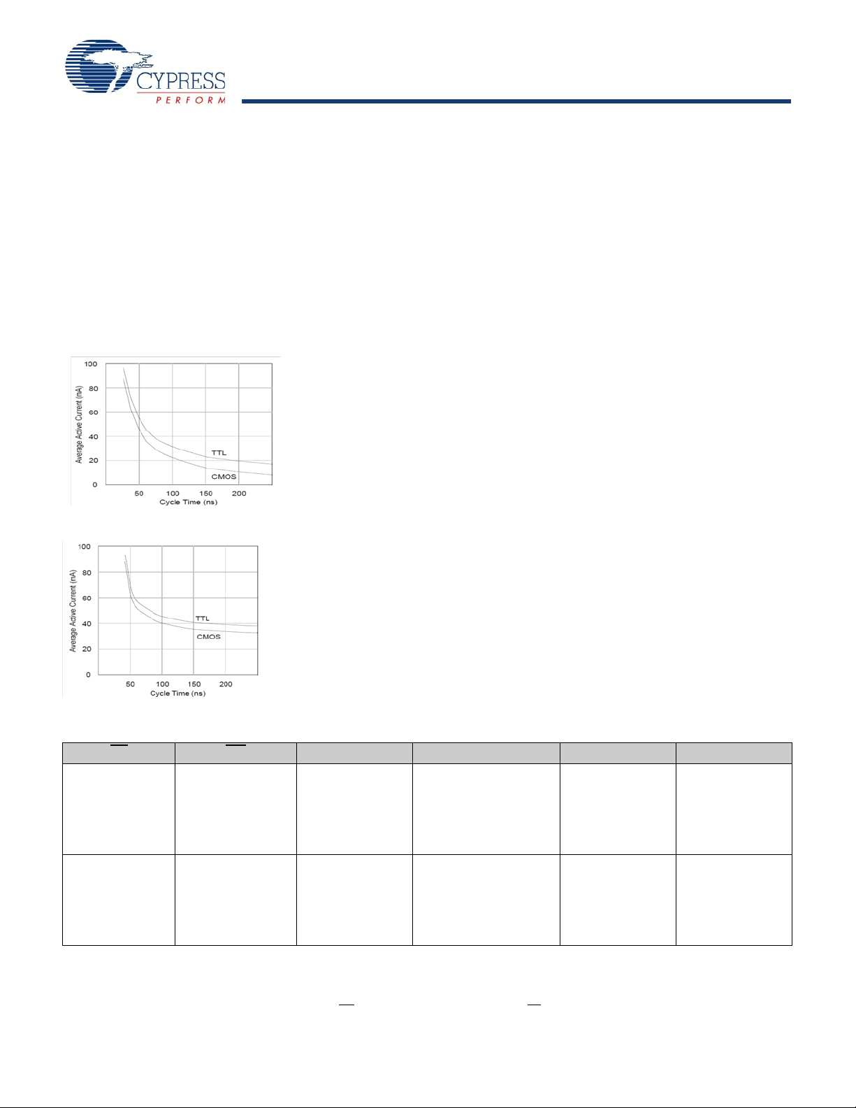
Low Average Active Power
CMOS technology provides the STK11C68 the benefit of
drawing significantly less current when it is cycled at times longer
than 50 ns. Figure 2 shows the relationship between I
Read or Write cycle time. Worst case current consumption is
shown for both CMOS and TTL input levels (commercial temperature range, VCC = 5.5V, 100% duty cycle on chip enable). Only
standby current is drawn when the chip is disabled. The overall
CC
and
Document Number: 001-50638 Rev. ** Page 3 of 16
[+] Feedback
Page 4
STK11C68
average current drawn by the STK11C68 depends on the
Note
1. The six consecutive addresses must be in the order listed. WE
must be high during all six consecutive CE controlled cycles to enable a nonvolatile cycle.
following items:
■
The duty cycle of chip enable
■
The overall cycle rate for accesses
■
The ratio of Reads to Writes
■
CMOS versus TTL input levels
■
The operating temperature
■
The VCC level
■
IO loading
Figure 2. Current Versus Cycle Time (Read)
Figure 3. Current Versus Cycle Time (Write)
Best Practices
nvSRAM products have been used effectively for over 15 years.
While ease of use is one of the product’s main system values,
experience gained working with hundreds of applications has
resulted in the following suggestions as best practices:
■
The nonvolatile cells in an nvSRAM are programmed on the
test floor during final test and quality assurance. Incoming
inspection routines at customer or contract manufacturer’s
sites sometimes reprograms these values. Final NV patterns
are typically repeating patterns of AA, 55, 00, FF, A5, or 5A.
The end product’s firmware should not assume that an NV array
is in a set programmed state. Routines that check memory
content values to determine first time system configuration,
■
cold or warm boot status, and so on must always program a
unique NV pattern (for example, complex 4-byte pattern of 46
E6 49 53 hex or more random bytes) as part of the final system
manufacturing test to ensure these system routines work
consistently.
■
Power up boot firmware routines should rewrite the nvSRAM
into the desired state. While the nvSRAM is shipped in a preset
state, best practice is to again rewrite the nvSRAM into the
desired state as a safeguard against events that might flip the
bit inadvertently (program bugs, incoming inspection routines,
and so on).
Table 1. Hardware Mode Selection
CE WE A12–A0 Mode IO Notes
L H 0x0000
L H 0x0000
Document Number: 001-50638 Rev. ** Page 4 of 16
Read SRAM
0x1555
0x0AAA
0x1FFF
0x10F0
0x0F0F
Read SRAM
Read SRAM
Read SRAM
Read SRAM
Nonvolatile STORE
Read SRAM
0x1555
0x0AAA
0x1FFF
0x10F0
0x0F0E
Read SRAM
Read SRAM
Read SRAM
Read SRAM
Nonvolatile RECALL
Output Data
Output Data
Output Data
Output Data
Output Data
Output High Z
Output Data
Output Data
Output Data
Output Data
Output Data
Output High Z
[1]
[1]
[+] Feedback
Page 5
STK11C68
Maximum Ratings
Note
2. CE
> VIH does not produce standby current levels until any nonvolatile cycle in progress has timed out.
Exceeding maximum ratings may shorten the useful life of the
device. These user guidelines are not tested.
Storage Tem perature ................................. –65°C to +150°C
Temperature under bias..............................–55°C to +125°C
Supply Voltage on VCC Relative to GND..........–0.5V to 7.0V
Voltage on Input Relative to Vss............–0.6V to V
Voltage on DQ
...................................–0.5V to Vcc + 0.5V
0-7
+ 0.5V
CC
Power Dissipation .........................................................1.0W
DC Output Current (1 output at a time, 1s duration).... 15 mA
Operating Range
Range
Commercial 0°C to +70°C 4.5V to 5.5V
Industrial -40°C to +85°C 4.5V to 5.5V
Ambient
Temperature
V
CC
DC Electrical Characteristics
Over the operating range (VCC = 4.5V to 5.5V)
Parameter Description Test Conditions Min Max Unit
I
CC1
I
CC2
I
CC3
I
SB1
[2]
Average VCC Current tRC = 25 ns
t
= 35 ns
RC
t
= 45 ns
RC
Dependent on output loading and cycle rate.
Values obtained without output loads.
I
= 0 mA.
OUT
Average VCC Current
during STORE
Average VCC Current at
= 200 ns, 5V, 25°C
t
RC
Typical
VCC Standby Current
(Standby, Cycling TTL
Input Levels)
All Inputs Do Not Care, VCC = Max
Average current for duration t
WE
> (VCC – 0.2V). All other inputs cycling.
Dependent on output loading and cycle rate. Values obtained
without output loads.
tRC = 25 ns, CE > V
tRC = 35 ns, CE > V
tRC = 45 ns, CE > V
IH
IH
IH
Commercial 90
75
65
Industrial 90
75
65
3mA
STORE
10 mA
Commercial 27
23
20
Industrial 28
24
21
[2]
I
SB2
I
IX
I
OZ
V
V
V
V
IH
IL
OH
OL
VCC Standby Current CE > (VCC – 0.2V). All others V
– 0.2V). Standby current level after
(V
CC
nonvolatile cycle is complete.
< 0.2V or >
IN
Inputs are static. f = 0 MHz.
Input Leakage Current VCC = Max, VSS < V
Off State Output
VCC = Max, VSS < V
Leakage Current
< V
IN
CC
< VCC, CE or OE > V
IN
Input HIGH Voltage 2.2 VCC +
Input LOW Voltage VSS – 0.5 0.8 V
Output HIGH Voltage I
Output LOW Voltage I
= –4 mA 2.4 V
OUT
= 8 mA 0.4 V
OUT
Commercial 750 μA
Industrial 1500 μA
-1 +1 μA
or WE < V
IH
IL
-5 +5 μA
0.5
Data Retention and Endurance
Parameter Description Min Unit
DATA
NV
C
R
Data Retention 100 Years
Nonvolatile STORE Operations 1,000 K
mA
mA
mA
mA
mA
mA
mA
mA
mA
mA
mA
mA
V
Document Number: 001-50638 Rev. ** Page 5 of 16
[+] Feedback
Page 6

STK11C68
Capacitance
5.0V
Output
30 pF
R1 480Ω
R2
255Ω
Input Pulse Levels....................................................0V to 3V
Input Rise and Fall Times (10% to 90%)...................... <
5 ns
Input and Output Timing Reference Levels.................... 1.5V
Note
3. These parameters are guaranteed by design and are not tested.
In the following table, the capacitance parameters are listed.
Parameter Description Test Conditions Max Unit
C
C
IN
OUT
Input Capacitance TA = 25°C, f = 1 MHz,
V
= 0 to 3.0V
Output Capacitance 7pF
CC
[3]
8pF
Thermal Resistance
In the following table, the thermal resistance parameters are listed.
Parameter Description Test Conditions 28-SOIC 28-CDIP 28-LCC Unit
Θ
Θ
JA
JC
Thermal Resistance
(Junction to Ambient)
Thermal Resistance
(Junction to Case)
Test conditions follow standard test methods
and procedures for measuring thermal
impedance, per EIA / JESD51.
Figure 4. AC Test Loads
[3]
TBD TBD TBD °C/W
TBD TBD TBD °C/W
AC Test Conditions
Document Number: 001-50638 Rev. ** Page 6 of 16
[+] Feedback
Page 7

STK11C68
AC Switching Characteristics
W
5&
W
$$
W
2+$
$''5(66
'4'$7$287
'$7$9$/,'
$''5(66
W
5&
&(
W
$&(
W
/=&(
W
3'
W
+=&(
2(
W
'2(
W
/=2(
W
+=2(
'$7$9$/,'
$&7,9(
67$1'%<
W
38
'4'$7$287
,&&
Notes
4. WE
must be High during SRAM Read cycles.
5. I/O state assumes CE
and OE < VIL and WE > VIH; device is continuously selected.
6. Measured ±200 mV from steady state output voltage.
SRAM Read Cycle
Parameter
Cypress
Parameter
t
ACE
[4]
t
RC
[5]
t
AA
t
DOE
[5]
t
OHA
[6]
t
LZCE
[6]
t
HZCE
[6]
t
LZOE
[6]
t
HZOE
[3]
t
PU
[3]
t
PD
Alt
t
ELQV
t
AVAV, tELEH
t
AVQV
t
GLQV
t
AXQX
t
ELQX
t
EHQZ
t
GLQX
t
GHQZ
t
ELICCH
t
EHICCL
Chip Enable Access Time 25 35 45 ns
Read Cycle Time 25 35 45 ns
Address Access Time 25 35 45 ns
Output Enable to Data Valid 10 15 20 ns
Output Hold After Address Change 5 5 5 ns
Chip Enable to Output Active 5 5 5 ns
Chip Disable to Output Inactive 10 13 15 ns
Output Enable to Output Active 0 0 0 ns
Output Disable to Output Inactive 10 13 15 ns
Chip Enable to Power Active 0 0 0 ns
Chip Disable to Power Standby 25 35 45 ns
Switching Waveforms
Figure 5. SRAM Read Cycle 1: Address Controlled
Description
25 ns 35 ns 45 ns
Min Max Min Max Min Max
[4, 5]
Unit
Document Number: 001-50638 Rev. ** Page 7 of 16
Figure 6. SRAM Read Cycle 2: CE and OE Controlled
[4]
[+] Feedback
Page 8
STK11C68
SRAM Write Cycle
t
WC
t
SCE
t
HA
t
AW
t
SA
t
PWE
t
SD
t
HD
t
HZWE
t
LZWE
ADDRESS
CE
WE
DATA IN
DATA OUT
DATA VALID
HIGH IMPEDANCE
PREVIOUS DATA
t
WC
ADDRESS
t
SA
t
SCE
t
HA
t
AW
t
PWE
t
SD
t
HD
CE
WE
DATA IN
DATA OUT
HIGH IMPEDANCE
DATA VALID
Notes
7. If WE
is Low when CE goes Low, the outputs remain in the high impedance state.
8.
CE
or WE must be greater than VIH during address transitions.
Parameter
Cypress
Parameter
t
WC
t
PWE
t
SCE
t
SD
t
HD
t
AW
t
SA
t
HA
[6,7]
t
HZWE
[6]
t
LZWE
t
t
t
t
t
t
t
t
t
t
Alt
AVAV
WLWH, tWLEH
ELWH, tELEH
DVWH, tDVEH
WHDX, tEHDX
AVWH, tAVEH
AVWL, tAVEL
WHAX, tEHAX
WLQZ
WHQX
Switching Waveforms
25 ns 35 ns 45 ns
Description
Min Max Min Max Min Max
Unit
Write Cycle Time 25 35 45 ns
Write Pulse Width 20 25 30 ns
Chip Enable To End of Write 20 25 30 ns
Data Setup to End of Write 10 12 15 ns
Data Hold After End of Write 0 0 0 ns
Address Setup to End of Write 20 25 30 ns
Address Setup to Start of Write 0 0 0 ns
Address Hold After End of Write 0 0 0 ns
Write Enable to Output Disable 10 13 15 ns
Output Active After End of Write 5 5 5 ns
Figure 7. SRAM Write Cycle 1: WE Controlled
[7, 8]
Document Number: 001-50638 Rev. ** Page 8 of 16
Figure 8. SRAM Write Cycle 2: CE and OE Controlled
[7, 8]
[+] Feedback
Page 9

STK11C68
AutoStore INHIBIT or Power Up RECALL
V
CC
V
SWITCH
V
RESET
POWER-UP RECALL
DQ (DATA OUT)
STORE INHIBIT
5V
t
HRECALL
POWER-UP
RECALL
BROWN OUT
STORE INHIBIT
NO RECALL
(V
CC
DID NOT GO
BELOW V
RESET
)
BROWN OUT
STORE INHIBIT
NO RECALL
(V
CC
DID NOT GO
BELOW V
RESET
)
BROWN OUT
STORE INHIBIT
RECALL WHEN
V
CC
RETURNS
ABOVE V
SWITCH
Note
9. t
HRECALL
starts from the time VCC rises above V
SWITCH
.
Parameter Alt Description
t
HRECALL
t
STORE
V
SWITCH
V
RESET
[9]
t
RESTORE
t
HLHZ
Power up RECALL Duration 550 μs
STORE Cycle Duration 10 ms
Low Voltage Trigger Level 4.0 4.5 V
Low Voltage Reset Level 3.6 V
Switching Waveform
Figure 9. AutoStore INHIBIT/Power Up RECALL
STK11C68
Min Max
Unit
Document Number: 001-50638 Rev. ** Page 9 of 16
[+] Feedback
Page 10

STK11C68
Software Controlled STORE/RECALL Cycle
t
RC
t
RC
t
SA
t
SCE
t
HACE
t
STORE
/ t
RECALL
DATA VALID
DATA VALID
6#SSERDDA1#SSERDDA
HIGH IMPEDANCE
ADDRESS
CE
OE
DQ (DATA)
Notes
10.The software sequence is clocked on the falling edge of CE
without involving OE (double clocking aborts the sequence).
11.The six consecutive addresses must be read in the order listed in Table 1 on page 4. WE
must be HIGH during all six consecutive cycles.
The software controlled STORE/RECALL cycle follows.
Parameter Alt Description
t
RC
[10]
t
SA
[10]
t
CW
t
HACE
t
RECALL
[10]
[10]
t
AVAV
t
AVEL
t
ELEH
t
ELAX
STORE/RECALL Initiation Cycle Time 25 35 45 ns
Address Setup Time 0 0 0 ns
Clock Pulse Width 20 25 30 ns
Address Hold Time 20 20 20 ns
RECALL Duration 20 20 20 μs
[10, 11]
25 ns 35 ns 45 ns
Min Max Min Max Min Max
Unit
Switching Waveform
Figure 10. CE Controlled Software STORE/RECALL Cycle
[11]
Document Number: 001-50638 Rev. ** Page 10 of 16
[+] Feedback
Page 11

STK11C68
Ordering Information
Part Numbering Nomenclature
Packaging Option:
TR = Tape and Reel
Blank = Tube
Speed:
25 - 25 ns
35 - 35 ns
Package:
S = Plastic 28-pin 330 mil SOIC
STK11C68 - S F 45 I TR
Temperature Range:
Blank - Commercial (0 to 70°C)
C = Ceramic 28-pin 300 mil DIP
L = Ceramic 28-pin 350 mil LLC
Lead Finish
F = 100% Sn (Matte Tin)
45 - 45 ns
I - Industrial (-40 to 85°C)
Speed (n s) Ordering Code Package Diagram Packag e Type Operating Range
25 STK11C68-SF25TR 001-85058 28-Pin SOIC (330 mil) Commercial
STK11C68-SF25 001-85058 28-Pin SOIC (330 mil)
STK11C68-SF25ITR 001-85058 28-Pin SOIC (330 mil) Industrial
STK11C68-SF25I 001-85058 28-Pin SOIC (330 mil)
35 STK11C68-SF35TR 001-85058 28-Pin SOIC (330 mil) Commercial
STK11C68-SF35 001-85058 28-Pin SOIC (330 mil)
STK11C68-C35 001-51 695 28-Pin CDIP (300 mil)
STK11C68-L35 001-51696 28-Pin LCC (350 mil)
STK11C68-SF35ITR 001-85058 28-Pin SOIC (330 mil) Industrial
STK11C68-SF35I 001-85058 28-Pin SOIC (330 mil)
STK11C68-C35I 001-51695 28-Pin CDIP (300 mil)
STK11C68-L35I 001-51696 28-Pin LCC (350 mil)
Document Number: 001-50638 Rev. ** Page 11 of 16
[+] Feedback
Page 12

STK11C68
Ordering Information
Speed (n s) Ordering Code Package Diagram Packag e Type Operating Range
45 STK11C68-SF45TR 001-85058 28-Pin SOIC (330 mil) Commercial
STK11C68-SF45 001-85058 28-Pin SOIC (330 mil)
STK11C68-C45 001-51 695 28-Pin CDIP (300 mil)
STK11C68-L45 001-51696 28-Pin LCC (350 mil)
STK11C68-SF45ITR 001-85058 28-Pin SOIC (330 mil) Industrial
STK11C68-SF45I 001-85058 28-Pin SOIC (330 mil)
STK11C68-C45I 001-51695 28-Pin CDIP (300 mil)
STK11C68-L45I 001-51696 28-Pin LCC (350 mil)
All parts are Pb-free. The above table contains Final information. Contact your local Cypress sales representative for availability of these parts
(continued)
Document Number: 001-50638 Rev. ** Page 12 of 16
[+] Feedback
Page 13

STK11C68
Package Diagrams
51-85058 *A
Figure 11. 28-Pin (330 Mil) SOIC (51-85058)
Document Number: 001-50638 Rev. ** Page 13 of 16
[+] Feedback
Page 14

STK11C68
Package Diagrams
001-51695 **
(continued)
Figure 12. 28-Pin (300 Mil) Side Braze DIL (001-51695)
Document Number: 001-50638 Rev. ** Page 14 of 16
[+] Feedback
Page 15

STK11C68
Package Diagrams
1. ALL DIMEN SION ARE IN INCH ES AND MILLIM ETERS [MIN/MA X]
2. JEDEC 95 OUTLINE# MO-041
3. PACKAGE WEIGHT : TBD
001-51696 **
(continued)
Figure 13. 28-Pad (350 Mil) LCC (001-51696)
Document Number: 001-50638 Rev. ** Page 15 of 16
[+] Feedback
Page 16

STK11C68
Document History Page
Document Title: STK11C68 64 Kbit (8K x 8) SoftStore nvSRAM
Document Number: 001-50638
Rev. ECN No.
Orig. of
Change
Submission
Date
Description of Change
** 2625084 GVCH/PYRS 01/30/09 New data sheet
Sales, Solutions, and Legal Information
Worldwide Sales and Design Support
Cypress maintains a worldwide network of offices, solution centers, manufacturer’s representatives, and distributors. T o find the office
closest to you, visit us at cypress.com/sales.
Products
PSoC psoc.cypress.com
Clocks & Buffers clocks.cypress.com
Wireless wireless.cypress.com
Memories memory.cypress.com
Image Sensors image.cypress.com
PSoC Solutions
General psoc.cypress.com/solutions
Low Power/Low Voltage psoc.cypress.com/low-power
Precision Analog psoc.cypress.com/precision-analog
LCD Drive psoc.cypress.com/lcd-drive
CAN 2.0b psoc.cypress.com/can
USB psoc.cypress.com/usb
© Cypress Semiconductor Corporation, 2009. The information contained herein is subject to change without notice. Cypress Semiconductor Corporation assumes no responsibility for the use of any
circuitry other than circuitry embodied in a Cypress product. Nor does it convey or imply any license under patent or other rights. Cypress products are not warranted nor intended to be used for medical,
life support, life saving, critical control or safety applications, unless pursuant to an express written agreement with Cypress. Furthermore, Cypress does not author ize its products for use as critic al
components in life-support systems where a malfunction or failure may reasonably be expected to result in significant injury to the user. The inclusion of Cypress products in life-support systems
application implies that the manufacturer assumes all risk of such use and in doing so indemnifies Cypress against all charges.
Any Source Code (software and/or firmware) is owned by Cypress Semiconductor Corporation (Cypress) and is protected by and subject to worldwide patent protection (United States and foreign),
United States copyrigh t laws and interna tional tr eaty pr ovision s. Cypr ess here by gra nt s to lic ensee a p erson al, no n-excl usive , non- tran sferabl e license to copy, use, modify, create derivative works of,
and compile the Cypress Source Code and derivative works for the sole purpose of creating custom software and or firmware in support of licensee product to be used only in conju nction with a Cypress
integrated circuit as specified in the ap plicable agr eement. Any reprod uction, modificati on, translation, co mpilation, or re presentatio n of this Source Code except as spe cified above is prohibited wi thout
the express written permission of Cypress.
Disclaimer: CYPRESS MAKES NO WARRANTY OF ANY KIND, EXPRESS OR IMPLIED, WITH REGARD TO THIS MATERIAL, INCLUDING, BUT NOT LIMITED TO, THE IMPLIED WARRANTIES
OF MERCHANTABILITY AND FITNESS FOR A PARTICULAR PURPOSE. Cypress reserves the right to make changes without further notice to the materials described herein. Cypress does not
assume any liability arising out of the app licati on or us e of an y product or circ uit de scrib ed herei n. Cypr ess does n ot auth orize it s product s for use a s critical component s in life-suppo rt systems where
a malfunction or failure may reasonably be expected to result in significant injury to the user. The inclusion of Cypress’ product in a life-support systems application implies that the manufacturer
assumes all risk of such use and in doing so indemnifies Cypress against all charges.
Use may be limited by and subject to the applicable Cypress software license agreement.
Document Number: 001-50638 Rev. ** Revised January 30, 2009 Page 16 of 16
AutoStore and Quant umTrap ar e registered tradem arks of Cypress Semico nductor Corporat ion. All product s and company n ames mentioned in this document may be the trademarks of their respective
holders.
[+] Feedback
 Loading...