

Page 1
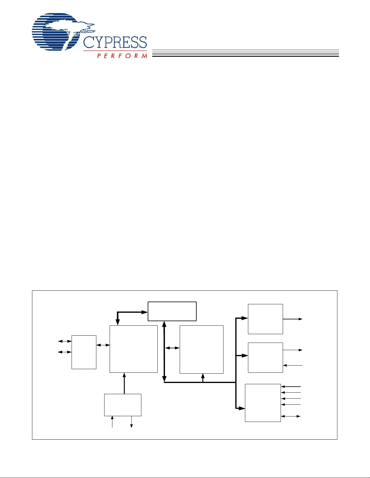
SL811HS Embedded USB Host/Slave Controller
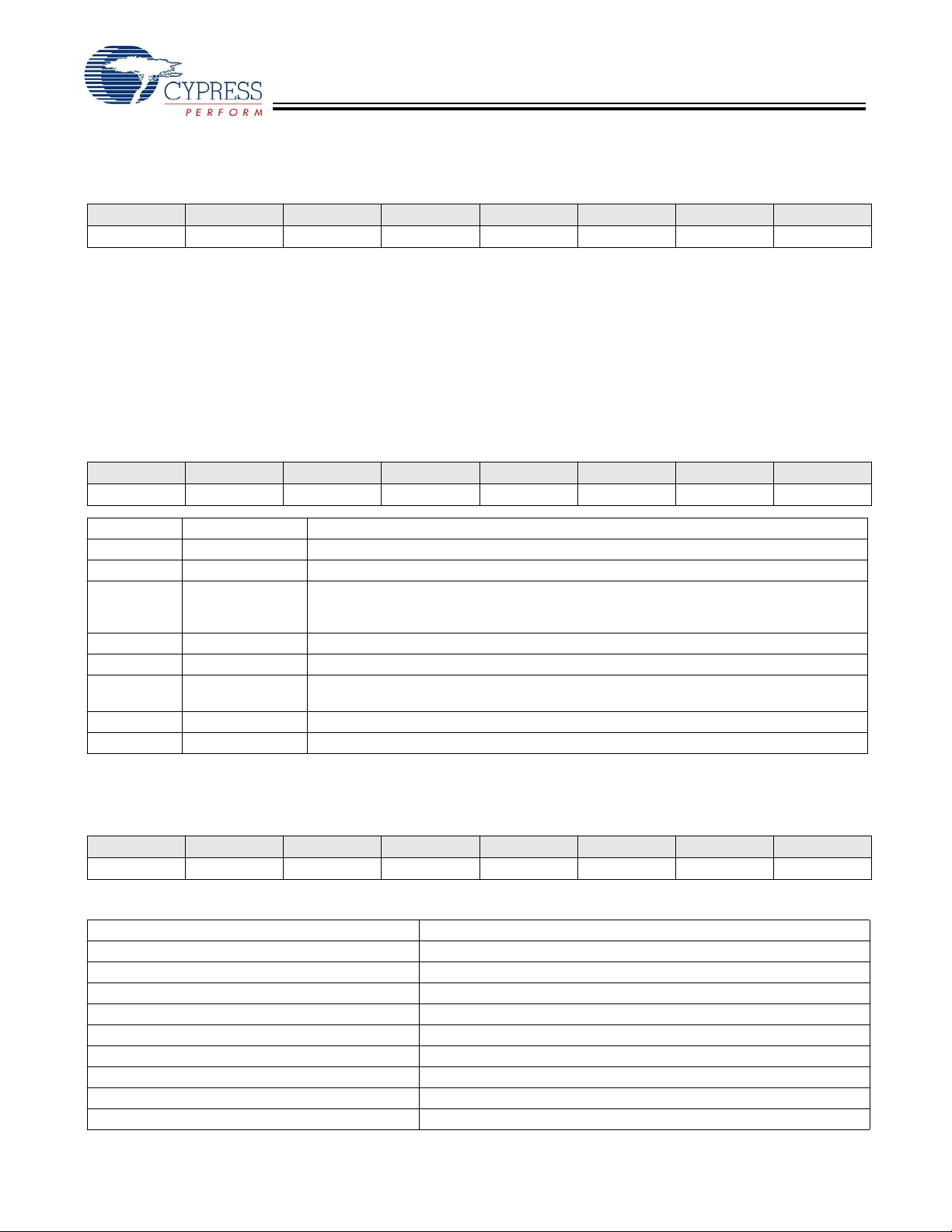
SL811HS
Features
X1 X2
D
+
D-
INTR
nWR
nRD
nCS
nRST
D0-7
GENERATOR
USB
Root
HUB
XCVRS
SERIAL
INTER F ACE
ENGINE
256 Byte RAM
BUFFERS
CONTROL
REGISTERS
INTERRUPT
CLOCK
&
CONTROLLER
PROCESSOR
INTER F ACE
M a s te r/Slav e
Controller
nDRQ
nDACK
DMA
Interface
Block Diagram
Introduction
• First USB Host/Slave controller for embedded systems in
the market with a standard microprocessor bus interface
• Supports both full speed (12 Mbps) and low speed (1.5
Mbps) USB transfer in both master and slave modes
• Conforms to USB Specification 1.1 for full- and low speed
• Operates as a single USB host or slave under software
control
• Automatic detection of either low- or full speed devices
• 8-bit bidirectional data, port I/O (DMA supported in slave
mode)
• On-chip SIE and USB transceivers
• On-chip single root HUB support
• 256-byte internal SRAM buffer
• Ping-pong buffers for improved performance
• Operates from 12 or 48 MHz crystal or oscillator (built-in
DPLL)
• 5V-tolerant interface
• Suspend/resume, wake up, and low-power modes are
supported
• Auto-generation of SOF and CRC5/16
• Auto-address increment mode, saves memory
READ/WRITE cycles
• Development kit including source code drivers is available
• 3.3V power source, 0.35 micron CMOS technology
• Available in both a 28-pin PLCC package and a 48-pin
TQFP package
The SL811HS is an Embedded USB Host/Slave Controller
capable of communicating in either full speed or low speed.
The SL811HS interfaces to devices such as microprocessors,
microcontrollers, DSPs, or directly to a variety of buses such
as ISA, PCMCIA, and others. The SL811HS USB Host
Controller conforms to USB Specification 1.1.
The SL811HS incorporates USB Serial Interface functionality
along with internal full or low speed transceivers. The
SL811HS supports and operates in USB full speed mode at 12
Mbps, or in low speed mode at 1.5 Mbps. When in host mode,
the SL811HS is the master and controls the USB bus and the
devices that are connected to it. In peripheral mode, otherwise
known as a slave device, the SL811HS operates as a variety
of full- or low speed devices.
The SL811HS data port and microprocessor interface provide
an 8-bit data path I/O or DMA bidirectional, with interrupt
support to allow easy interface to standard microprocessors or
microcontrollers such as Motorola or Intel CPUs and many
others. The SL811HS has 256-bytes of internal RAM which is
used for control registers and data buffer.
The available package types offered are a 28-pin PLCC
(SL811HS) and the lead-free packages are a 28-pin
(SL811HS-JCT) and a 48-pin (SL811HST-AXC) package. All
packages operate at 3.3 VDC. The I/O interface logic is
5V-tolerant.
Cypress Semiconductor Corporation • 198 Champion Court • San Jose, CA 95134-1709 • 408-943-2600
Document 38-08008 Rev. *D Revised February 2, 2007
Page 2

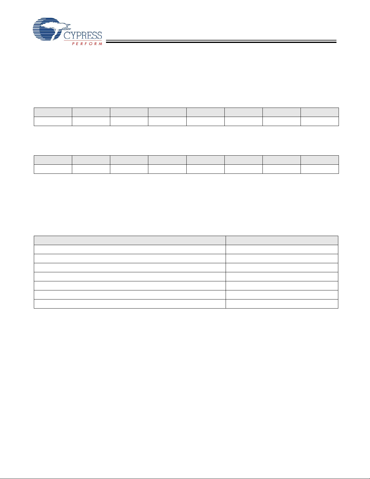
SL811HS
0x00 – 0x0F Control
and status registers
0x10 – 0xFF
USB data buffer
240 bytes
16 bytes
0x00 – 0x39
Control/status registers
and endpoint
control/status registers
0x40 – 0xFF
USB data buffer
192 bytes
64 bytes
Host Mode Memory Map Peripheral Mode Memory Map
Figure 1. Memory Map
Data Port, Microprocessor Interface
The SL811HS microprocessor interface provides an 8-bit
bidirectional data path along with appropriate control lines to
interface to external processors or controllers. Programmed
I/O or memory mapped I/O designs are supported through the
8-bit interface, chip select, read and write input strobes, and a
single address line, A0.
Access to memory and control register space is a simple two
step process, requiring an address Write with A0 = ’0’, followed
by a register/memory Read or Write cycle with address line A0
= ’1’.
In addition, a DMA bidirectional interface in slave mode is
available with handshake signals such as nDRQ, nDACK,
nWR, nRD, nCS and INTRQ.
The SL811HS WRITE or READ operation terminates when
either nWR or nCS goes inactive. For devices interfacing to
the SL811HS that deactivate the Chip Select nCS before the
Write nWR, the data hold timing must be measured from the
nCS and will be the same value as specified. Therefore, both
®
Intel
- and Motorola-type CPUs work easily with the SL811HS
without any external glue logic requirements.
DMA Controller (slave mode only)
In applications that require transfers of large amounts of data
such as scanner interfaces, the SL811HS provides a DMA interface. This interface supports DMA READ or WRITE transfers to the SL811HS internal RAM buffer , it is done through the
microprocessor data bus via two control lines (nDRQ - Data
Request and nDACK - Data Acknowledge), along with the
nWR line and controls the data flow into the SL811HS. The
SL811HS has a count register that allows selection of programmable block sizes for DMA transfer. The control signals,
both nDRQ and nDACK, are designed for compatibility with
standard DMA interfaces.
Interrupt Controller
The SL811HS interrupt controller provides a single output
signal (INTRQ) that is activated by a number of programmable
events that may occur as result of USB activity. Control and
status registers are provided to allow the user to select single
or multiple events, which generate an interrupt (assert INTRQ)
and let the user view interrupt status. The interrupts are
cleared by writing to the Interrupt Status Register.
Buffer Memory
The SL811HS cont ains 256 bytes of internal memory used for
USB data buffers, control registers, and status registers. When
in master mode (host mode), the memory is defined where the
first 16 bytes are registers and the remaining 240 bytes are
used for USB data buffers. When in slave mode (peripheral
mode), the first 64 bytes are used for the four endpoint control
and status registers along with the various other registers. This
leaves 192 bytes of endpoint buffer space for USB data
transfers.
Access to the registers and data memory is through the 8-bit
external microprocessor data bus, in either indexed or direct
addressing. Indexed mode uses the Auto Address Increment
mode described in Auto Address Increment Mode, where
direct addressing is used to READ/WRITE to an individual
address.
USB transactions are automatically routed to the memory
buffer that is configured for that transfer. Control registers are
provided so that pointers and block sizes in buffer memory are
determined and allocated.
Auto Address Increment Mode
The SL811HS supports auto increment mode to reduce READ
and WRITE memory cycles. In this mode, the microcontroller
needs to set up the address only once. Whenever any subsequent DAT A is accessed, the internal address counter advances to the next address location.
Auto Address Increment Example. To fill the data buffer
that is configured for address 10h, follow these steps:
1. Write 10h to SL811HS with A0 LOW . This sets the memory
address that is used for the next operation.
2. Write the first data byte into address 10h by doing a write
operation with A0 HIGH. An example is a Get Descriptor;
the first byte that is sent to the device is 80h
(bmRequestType) so you would write 80h to address 10h.
3. Now the internal RAM address pointer is set to 11h. So, by
doing another write with A0 HIGH, RAM address location
11h is written with the data. Con tinuing with the Get
Descriptor example, a 06h is written to address 11h for the
bRequest value.
4. Repeat Step 3 until all the required bytes are written as
necessary for a transfer. If auto-increment is not used, you
write the address value each time before writing the data
as shown in Step 1.
The advantage of auto address increment mode is that it
reduces the number of required SL811HS memory
READ/WRITE cycles to move data to/from the device. For
example, transferring 64 bytes of data to/from SL811HS, using
auto increment mode, reduces the number of cycles to 1
address WRITE and 64 READ/WRITE data cycles, compared
to 64 address writes and 64 data cycles for random access.
Document 38-08008 Rev. *D Page 2 of 32
Page 3
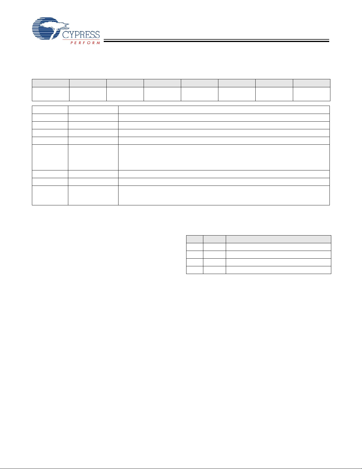
SL811HS
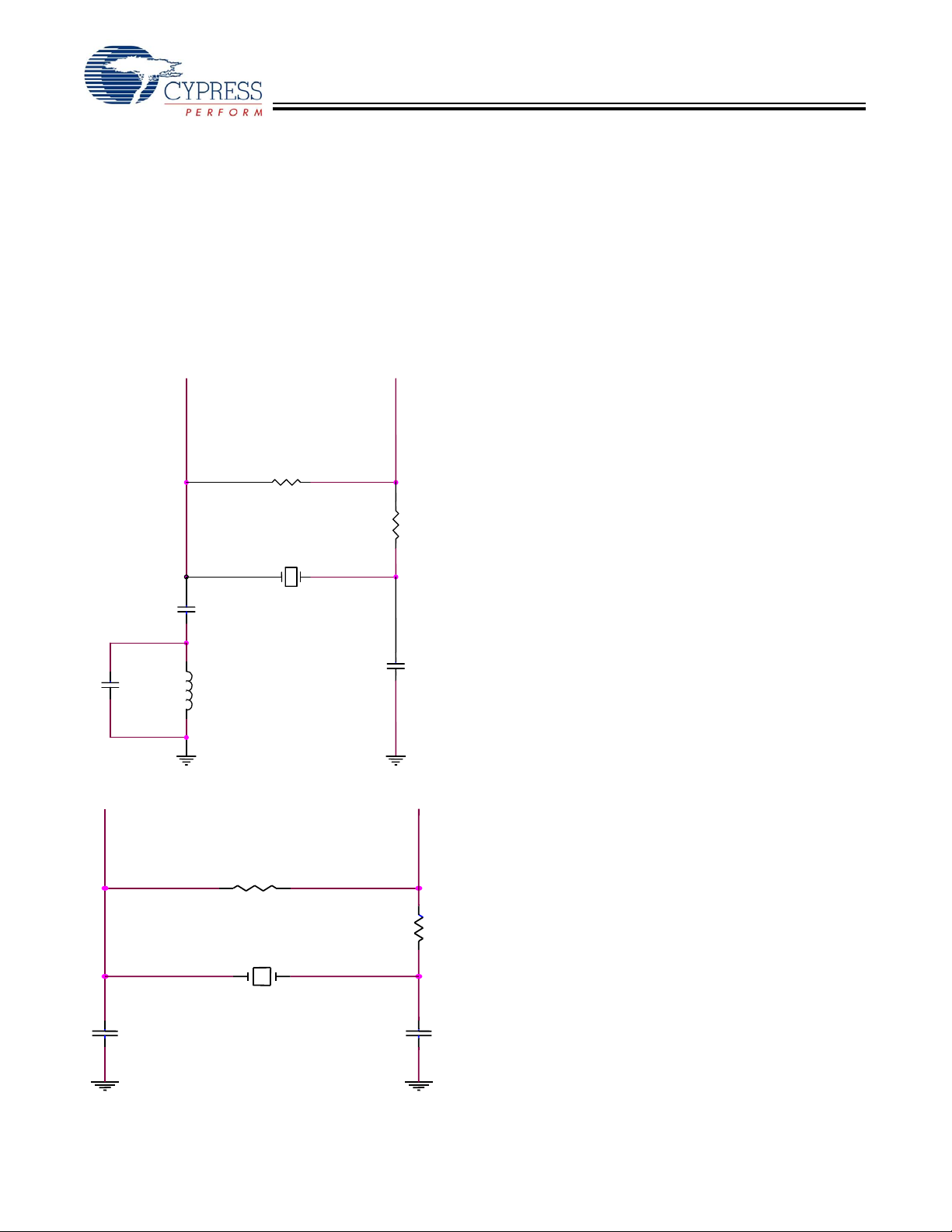
PLL Clock Generator
Note
1. CM (Clock Multiply) pin of the SL811HS must be tied to GND when 48 MHz crystal circuit or 48 MHz clock source is used.
Cbk
0.01 μF
Rs
100X1
48 MHz, series, 20-pF load
Cout
22 pF
Rf
1M
X2
Cin
22 pF
Lin
2.2 μH
X1
Figure 2. Full Speed 48 MHz Crystal Circuit
X1
12 MHz , series, 20-pF load
Rf
1M
Cin
22 pF
Cout
22 pF
Rs
100
X2X1
Figure 3. Optional 12 MHz Crystal Circuit
Either a 12 MHz or a 48 MHz external crystal is used with the
SL811HS
[1]
. Two pins, X1 and X2, are provided to connect a
low cost crystal circuit to the device as shown in Figure 2 and
Figure 3. Use an external clock source if available in the appli-
cation instead of the crystal circuit by connecting the source
directly to the X1 input pin. When a clock is used, the X2 pin
is not connected.
When the CM pin is tied to a logic 0, the internal PLL is
bypassed so the clock source must meet the timing requirements specified by the USB specification.
Typical Crystal Requirements
The following are examples of ‘typical requirements.’ Note that
these specifications are generally found as standard crystal
values and are less expensive than custom values. If crystals
are used in series circuits, load capacitance is not applicable.
Load capacitance of parallel circuits is a requirement. 48 MHz
third overtone crystals require the Cin/Lin filter to guarantee 48
MHz operation.
12 MHz Crystals:
Frequency Tolerance: ±100 ppm or better
Operating Temperature Range: 0°C to 70°C
Frequency: 12 MHz
Frequency Drift over Temperature: ± 50 ppm
ESR (Series Resistance): 60Ω
Load Capacitance: 10 pF min.
Shunt Capacitance: 7 pF max.
Drive Level: 0.1–0.5 mW
Operating Mode: fundamental
48 MHz Crystals:
Frequency Tolerance: ±100 ppm or better
Operating Temperature Range: 0°C to 70°C
Frequency: 48 MHz
Frequency Drift over Temperature: ± 50 ppm
ESR (Series Resistance): 40 Ω
Load Capacitance: 10 pF min.
Shunt Capacitance: 7 pF max.
Drive Level: 0.1–0.5 mW
Operating Mode: third overtone
USB Transceiver
The SL811HS has a built in transceiver that meets USB S pecification 1.1. The transceiver is capable of transmitting and
receiving serial data at USB full speed (12 Mbits) and low
speed (1.5 Mbits). The driver portion of the transceiver is differential while the receiver section is comprised of a differential
receiver and two single-ended receivers. Internally, the transceiver interfaces to the Serial Interface Engine (SIE) logic.
Externally, the transceiver connects to the physical layer of the
USB.
SL811HS Registers
Operation and control of the SL811HS is managed through
internal registers. When operating in Master/Host mode, the
first 16 address locations are defined as register space. In
Slave/Peripheral mode, the first 64 bytes are defined as
register space. The register definitions vary greatly between
each mode of operation and are defined separately in this
document (section “SL811HS Master (Host) Mode Registers”
on page 4 describes Host register definitions, while section
Document 38-08008 Rev. *D Page 3 of 32
Page 4
SL811HS
“SL811HS Slave Mode Registers” on page 12 describes Slave
register definitions). Access to the registers are through the
microprocessor interface similar to normal RAM accesses
(see “Bus Interface Timing Requirements” on page 26) and
provide control and status information for USB transactions.
Any write to control register 0FH enables the SL811HS full
features bit. This is an internal bit of the SL811HS that enables
additional features.
Table 1 shows the memory map and register mapping of the
SL811HS in master/host mode.
SL811HS Master (Host) Mode Registers
Table 1. SL811HS Master (Host) Register Summary
Register Name
SL811HS
USB-A Host Control Register 00h
USB-A Host Base Address 01h
USB-A Host Base Length 02h
USB-A Host PID, Device Endpoint
(Write)/USB Status (Read)
USB-A Host Device Address (Write)/Transfer
Count (Read)
Control Register 1 05h
Interrupt Enable Register 06h
Reserved Register Reserved
USB-B Host Control Register 08h
USB-B Host Base Address 09h
USB-B Host Base Length 0Ah
USB-B Host PID, Device Endpoint
(Write)/USB Status (Read)
USB-B Host Device Address (Write)/Transfer
Count (Read)
Status Register 0Dh
SOF Counter LOW (Write)/HW Revision Reg-
ister (Read)
SOF Counter HIGH and Control Register 2 0Fh
Memory Buffer 10H-FFh
SL811HS
(hex) Address
03h
04h
0Bh
0Ch
0Eh
The registers in the SL811HS are divided into two major
groups. The first group is referred to as USB Control registers.
These registers enable and provide status for control of USB
transactions and data flow. The second group of registers
provides control and status for all other operations.
All other register’s power up and reset in an unknown state and
firmware for initialization.
USB Control Registers
Communication and data flow on the USB bus uses the
SL811HS’ USB A-B Control registers. The SL811HS communicates with any USB Device function and any specific
endpoint via the USB-A or USB-B register sets.
The USB A-B Host Control registers are used in an overlapped
configuration to manage traffic on the USB bus. The USB Host
Control register also provides a means to interrupt an external
CPU or microcontroller when one of the USB protocol transactions is completed. Table 1 and Table 2 show the two sets of
USB Host Control registers, the ’A’ set and ’B’ set. The two
register sets allow for overlapping operation. When one set of
parameters is being set up, the other is transferring. On
completion of a transfer to an endpoint, the next operation is
controlled by the other register set.
Note The USB-B register set is used only when SL811HS
mode is enabled by initializing register 0FH.
The SL811HS USB Host Control has two groups of five
registers each which map in the SL811HS memory space.
These registers are defined in the following tables.
SL811HS Host Control Registers.
Table 2. SL811HS Host Control Registers
Register Name SL811H
USB-A Host Control Register 00h
USB-A Host Base Address 01h
USB-A Host Base Length 02h
USB-A Host PID, Device Endpoint
(Write)/USB Status (Read)
USB-A Host Device Address (Write)/Transfer
Count (Read)
USB-B Host Control Register 08h
USB-B Host Base Address 09h
USB-B Host Base Length 0Ah
USB-B Host PID, Device Endpoint
(Write)/USB Status (Read)
USB-B Host Device Address (Write)/Transfer
Count (Read)
SL811HS
(hex) Address
03h
04h
0Bh
0Ch
Register Values on Power Up and Reset
The following registers initialize to zero on power up and reset:
• USB-A/USB-B Host Control Register [00H, 08H] bit 0 only
• Control Register 1 [05H]
• USB Address Register [07H]
• Current Data Set/Hardware Revision/SOF Counter LOW
Register [0EH]
Document 38-08008 Rev. *D Page 4 of 32
Page 5
SL811HS
USB-A/USB-B Host Control Registers [Address = 00h, 08h] .
Table 3. USB-A/USB-B Host Control Register Definition [Address 00h, 08h]
Bit 7 Bit 6 Bit 5 Bit 4 Bit 3 Bit 2 Bit 1 Bit 0
Preamble Data T oggle Bit SyncSOF ISO Reserved Direction Enable Arm
Bit Position Bit Name Function
7 Preamble If bit = ’1’ a preamble token is transmitted before transfer of low speed packet. If bit = ’0’,
6 Data Toggle Bit ’0’ if DATA0, ’1’ if DATA1 (only used for OUT tokens in host mode).
5 SyncSOF ’1’ = Synchronize with the SOF transfer when operating in FS only.
4 ISO When set to ’1’, this bit allows Isochronous mode for this packet.
3 Reserved Bit 3 is reserved for future use.
2 Direction When equal to ’1’ transmit (OUT). When equal to ’0’ receive (IN).
1 Enable If Enable = ’1’, this bit allows transfers to occur. If Enable = ’0’, USB transactions are ignored.
0 Arm Allows enabled transfers when Arm = ’1’. Cleared to ’0’ when transfer is complete (when
preamble generation is disabled.
• The SL811HS automatically generates preamble packets when bit 7 is set. This bit is only
used to send packets to a low speed device through a hub. To communicate to a full
speed device, this bit is set to ‘0’. For example, when SL811HS communicates to a low
speed device via the HUB:
— Set SL811HS SIE to operate at full speed, i.e., bit 5 of register 05h (Control Register 1)
= ’0’.
— Set bit 6 of register 0Fh (Control Register 2) = ’0’. Set correct polarity of DAT A+ and
DATA– state for full speed.
— Set bit 7, Preamble bit, = ’1’ in the Host Control registe r.
• When SL811HS communicates directly to a low speed device:
— Set bit 5 of register 05h (Control Re gister 1) = ’1’.
— Set bit 6 of register 0Fh (Control Register 2) = ’1’, DAT A+ and DATA– polarity for low
speed.
— The state of bit 7 is ignored in this mode.
The SL811HS uses bit 5 to enable transfer of a data packet after a SOF p acket is transmitted.
When bit 5 = ‘1’, the next enabled packet is sent after next SOF . If bit 5 = ‘0’ the next packet
is sent immediately if the SIE is free. If operating in low speed, do not set this bit.
The Enable bit is used in conjunction with the Arm bit (bit 0 of this register) for USB transfers.
Done Interrupt is asserted).
Once the other SL81 1HS Control registers are configured (registers 01h-04h or 09h-0Ch) the Host Control register is programmed
to initiate the USB transfer. This register initiates the transfer when the Enable and Arm bit are set as described above.
USB-A/USB-B Host Base Address [Address = 01h, 09h] .
Table 4. USB-A/USB-B Host Base Address Definition [Address 01h, 09h]
Bit 7 Bit 6 Bit 5 Bit 4 Bit 3 Bit 2 Bit 1 Bit 0
HBADD7 HBADD6 HBADD5 HBADD4 HBADD3 HBADD2 HBADD1 HBADD0
The USB-A/B Base Address is a pointer to the SL811HS memory buffer location for USB reads and writes. When transferring
data OUT (Host to Device), the USB-A and USB-B Host Base Address registers can be set up before setting ARM on the USB-A
or USB-B Host Control register. When using a double buffer scheme, the Host Base Address could be set up with the first buffer
used for DATA0 data and the other for DATA1 data.
Document 38-08008 Rev. *D Page 5 of 32
Page 6
SL811HS
USB-A/USB-B Host Base Length [Address = 02h, 0Ah].
Table 5. USB-A / USB-B Host Base Length Definition [Address 02h, 0Ah]
Bit 7 Bit 6 Bit 5 Bit 4 Bit 3 Bit 2 Bit 1 Bit 0
HBL7 HBL6 HBL5 HBL4 HBL3 HBL2 HBL1 HBL0
The USB A/B Host Base Length register contains the maximum packet size transferred between the SL811HS and a slave USB
peripheral. Essentially, this designates the largest packet size that is transferred by the SL811HS. Base Length designates the
size of data packet sent or received. For example, in full speed BULK mode, the maximum packet length is 64 bytes. In ISO
mode, the maximum packet length is 1023 bytes since the SL811HS only has an 8-bit length; the maximum packet size for the
ISO mode using the SL811HS is 255 – 16 bytes (register space). When the Host Base length register is set to zero, a Zero-Length
packet is transmitted.
USB-A/USB-B USB Packet Status (Read) and Host PID, Device Endpoint (Write) [Address = 03h, 0Bh]. This register has
two modes dependent on whether it is read or written. When read, this register provides packet status and contains information
relative to the last packet that has been received or transmitted. This register is not valid for reading until after the Done interrupt
occurs, which causes the register to update.
Table 6. USB-A/USB-B USB Packet Status Register Definition when READ [Address 03h, 0Bh]
Bit 7 Bit 6 Bit 5 Bit 4 Bit 3 Bit 2 Bit 1 Bit 0
STALL NAK Overflow Setup Sequence Time-out Error ACK
Bit Position Bit Name Function
7 ST ALL Slave device returned a STALL.
6 NAK Slave device returned a NAK.
5 Overflow Overflow condition - maximum length exceeded during receives. For underflow, see
4 Setup This bit is not applicable for Host operation since a SETUP packet is generated by the host.
3 Sequence Sequence bit. ’0’ if DATA0, ’1’ if DATA1.
2 Time-out Timeout occurred. A timeout is defined as 18-bit times without a device response (in full
1 Error Error detected in transmission. Th is includes CRC5, CRC16, and PID errors.
0 ACK Transmission Acknowledge.
USB-A/USB-B Host Transfer Count Register (Read), USB Address (Write) [Address = 04h,
0Ch] on page 7.
speed).
When written, this register provides the PID and Endpoint information to the USB SIE engine used in the next transaction. All 16
Endpoints can be addressed by the SL811HS.
Table 7. USB-A / USB-B Host PID and Device Endpoint Register when WRITTEN [Address 03h, 0Bh]
Bit 7 Bit 6 Bit 5 Bit 4 Bit 3 Bit 2 Bit 1 Bit 0
PID3 PID2 PID1 PID0 EP3 EP2 EP1 EP0
PID[3:0]: 4-bit PID Field (See Table Below), EP[3:0]: 4-bit Endpoint Value in Binary.
PID TYPE D7-D4
SETUP 1101 (D Hex)
IN 1001 (9 Hex)
OUT 0001 (1 Hex)
SOF 0101 (5 Hex)
PREAMBLE 1100 (C Hex)
NAK 1010 (A Hex)
STALL 1110 (E Hex)
DATA0 0011 (3 Hex)
DATA1 1011 (B Hex)
Document 38-08008 Rev. *D Page 6 of 32
Page 7
SL811HS
USB-A/USB-B Host Transfer Count Register (Read), USB Address (Write) [Address = 04h, 0Ch]. This register has two
different functions depending on whether it is read or written. When read, this register contains the number of bytes remaining
(from Host Base Length value) after a packet is transferred. For example, if the Base Length register is set to 0x040 and an IN
T oken was sent to the peripheral device. If, after the transfer is complete, the value of the Host Transfer Count is 0x10, the number
of bytes actually transferred is 0x30. This is considered as an underflow indication.
Table 8. USB-A / USB-B Host Transfer Count Register when READ [Address 04h, 0Ch]
Bit 7 Bit 6 Bit 5 Bit 4 Bit 3 Bit 2 Bit 1 Bit 0
HTC7 HTC6 HTC5 HTC4 HTC3 HTC2 HTC1 HTC0
When written, this register contains the USB Device Address with which the Host communicates.
Table 9. USB-A / USB-B USB Address when WRITTEN [Address 04h, 0Ch]
Bit 7 Bit 6 Bit 5 Bit 4 Bit3 Bit 2 Bit 1 Bit 0
0 DA6 DA5 DA4 DA3 DA2 DA1 DA0
DA6-DA0 Device address, up to 127 devices can be addressed.
DA7 Reserved bit must be set to zero.
SL811HS Control Registers
The next set of registers are the Control registers and control more of the op eration of the chip instead of USB packet type of
transfers. Table 10 is a summary of the control registers.
Table 10. SL811HS Control Registers Summary
Register Name SL811H SL811HS (hex) Address
Control Register 1 05h
Interrupt Enable Register 06h
Reserved Register 07h
Status Register 0Dh
SOF Counter LOW (Write)/HW Revision Register (Read) 0Eh
SOF Counter HIGH and Control Register 2 0Fh
Memory Buffer 10h-FFh
Document 38-08008 Rev. *D Page 7 of 32
Page 8
SL811HS
Control Register 1 [Address = 05h]. The Control Register 1 enable s/di sables USB tran sfe r operation with con trol bits defined
Notes
2. Force K-State for low speed.
3. Force J-State for low speed.
as follows.
Ta ble 11. Control Register 1 [Address 05h]
Bit 7 Bit 6 Bit 5 Bit 4 Bit 3 Bit 2 Bit 1 Bit 0
Reserved Suspend USB Speed J-K state force USB Engine
Reserved Reserved SOF ena/dis
Reset
Bit Position Bit Name Function
7 Reserved ‘0’
6 Suspend ’1’ = enable, ’0’ = disable.
5 USB Speed ’0’ setup for full speed, ’1’ setup low speed.
4 J-K state force See Table 12.
3 USB Engine Reset USB Engine reset = ’1’. Normal set ’0’.
When a device is detected, the first thing that to do is to send it a USB Reset to force it into
its default address of zero. The USB 2.0 specification states that for a root hub a device
must be reset for a minimum of 50 mS.
2 Reserved Some existing firmware examples set bit 2, but it is not necessary.
1 Reserved ‘0’
0 SOF ena/dis ’1’ = enable auto Hardware SOF generation; ’0’ = disable.
In the SL811HS, bit 0 is used to enable hardware SOF autogeneration. The generation of
SOFs continues when set to ‘0’, but SOF tokens are not output to USB.
At powe -up this register is cleared to all zeros.
Low-power Modes [Bit 6 Control Register, Address 05h]
When bit 6 (Suspend) is set to ’1’, the power of the transmit
transceiver is turned off, the internal RAM is in suspend mode,
and the internal clocks are disabled.
Note Any activity on the USB bus (i.e., K-S t ate, etc.) resumes
normal operation. To resume normal operation from the CPU
side, a Data Write cycle (i.e., A0 set HIGH for a Data Write
cycle) is done. This is a special case and not a normal direct
write where the address is first written and then the data. To
resume normal operation from the CPU side, you must do a
Data Write cycle only.
Low Speed/Full Speed Modes [Bit 5 Control Register 1,
Address 05h]
The SL811HS is designed to communicate with either full- or
low speed devices. At power up bit 5 is LOW, i.e., for full
speed. There are two cases when communicating with a low
speed device. When a low speed device is connected directly
to the SL811HS, bit 5 of Register 05h is set to ’1’ and bit 6 of
register 0Fh, Polarity Swap, is set to ’1’ in order to change the
polarity of D+ and D–. When a low speed device is connected
via a HUB to SL811HS, bit 5 of Register 05h is set to ’0’ and
bit 6 of register 0Fh is set to ’0’ in order to keep the polarity of
D+ and D– for full speed. In addition, make sure that bit 7 of
USB-A/USB-B Host Control registers [00h, 08h] is set to ’1’ for
preamble generation.
J-K Programming States [Bits 4 and 3 of Control Register
1, Address 05h]
The J-K force state control and USB Engine Reset bits are
used to generate a USB reset condition. Forcing K-state is
used for Peripheral device remote wake up, resume, and other
modes. These two bits are set to zero on power up.
Ta ble 12. Control Register 1 Address 05h – Bits 3 and 4
Bit 4 Bit 3 Function
0 0 Normal operating mode
0 1 Force USB Reset, D+ and D– are set LOW (SE0)
1 0 Force J-State, D+ set HIGH, D– set LOW
1 1 Force K-State, D– set HIGH, D+ set LOW
[2]
[3]
USB Reset Sequence
After a device is detected, write 08h to the Control register
(05h) to initiate the USB reset, then wait for the USB reset time
(root hub should be 50 ms) and additionally some types of
devices such as a Forced J-state. Lastly, set the Control
register (05h) back to 0h. After the reset is complete, the
auto-SOF generation is enabled.
SOF Packet Generation
The SL811HS automatically computes the frame number and
CRC5 by hardware. No CRC or SOF generation is required by
external firmware for the SL811HS, although it can be done by
sending an SOF PID in the Host PID, Device Endpoint register.
T o enable SOF generation, assuming host mode is configured:
1. Set up the SOF interval in registers 0x0F and 0x0E.
2. Enable the SOF hardware generation in this register by
setting bit 0 = ‘1’.
3. Set the Arm bit in the USB-A Host Control register.
Document 38-08008 Rev. *D Page 8 of 32
Page 9
SL811HS
Interrupt Enable Register [Address = 06h]. The SL811HS
provides an Interrupt Request Output, which is activated for a
number of conditions. The Interrupt Enable register allows the
user to select conditions that result in an interrupt that is issued
to an external CPU through the INTRQ pin. A separate
Interrupt Status register reflects the reason for the interrupt.
Enabling or disabling these interrupts does not have an effect
on whether or not the corresponding bit in the Interrupt Status
register is set or cleared; it only determines if the interrupt is
Table 13. Interrupt Enable Register [Address 06h]
Bit 7 Bit 6 Bit 5 Bit 4 Bit 3 Bit 2 Bit 1 Bit 0
Reserved Device
Detect/Resume
Bit Position Bit Name Function
7 Reserved ‘0’
6 Device Detect/Resume Enable Device Detect/Resume Interrupt.
5 Inserted/Removed Enable Slave Insert/Remove Detection is used to enable/disable the device
4 SOF Timer 1 = Enable Interrupt for SOF Timer. This is typically at 1 mS intervals, although the
3 Reserved ‘0’
2 Reserved ‘0’
1 USB-B DONE USB-B Done Interrupt (see USB-A Done interrupt).
0 USB-A DONE USB-A Done Interrupt. The Done interrupt is triggered by one of the events that are
Inserted/
Removed
When bit 6 of register 05h (Control Register 1) is equal to ’1’, bit 6 of this register enables
the Resume Detect Interrupt. Otherwise, this bit is used to enable Device Detection
status as defined in the Interrupt Status register bit definitions.
inserted/removed interrupt.
timing is determined by the SOF Counter high/low registers.
To use this bit function, bit 0 of register 05h must be enabled and the SOF counter
registers 0E hand 0Fh must be initialized.
logged in the USB Packet Status register . The Done interrupt causes the Packet Status
register to update.
SOF Timer Reserved Reserved USB-B
routed to the INTRQ pin. The Interrupt Status register is
normally used in conjunction with the Interrupt Enable register
and can be polled in order to determine the con ditions that
initiated the interrupt (See the description for the Interrupt
Status Register). When a bit is set to ’1’ the corresponding
interrupt is enabled. So when the enabled interrupt occurs, the
INTRQ pin is asserted. The INTRQ pin i s a level interrupt,
meaning it is not deasserted until all enabled interrupts are
cleared.
DONE
USB-A
DONE
USB Address Register, Reserved, Address [Address = 07h]. This register is reserved for the device USB Address in Slave
operation. It should not be written by the user in host mode.
Registers 08h-0Ch Host-B registers. Registers 08h-0Ch have the same definition as registers 00h -04h except they apply to
Host-B instead of Host-A.
Document 38-08008 Rev. *D Page 9 of 32
Page 10
SL811HS
Interrupt Status Register, Address [Address = 0Dh]. The Interrupt Status register is a READ/WRITE register providing
interrupt status. Interrupts are cleared by writing to this register. To clear a specific interrupt, the register is written with corresponding bit set to ’1’.
Table 14. Interrupt Status Register [Address 0Dh]
Bit 7 Bit 6 Bit 5 Bit 4 Bit 3 Bit 2 Bit 1 Bit 0
D+ Device
Detect/Resume
Bit Position Bit Name Function
7 D+ Value of the Data+ pin.
6 Device Detect/Resume Device Detect/Resume Interrupt.
5 Insert/Remove Device Insert/Remove Detection.
4 SOF timer ‘1’ = Interrupt on SOF Timer.
3 Reserved ‘0’
2 Reserved ‘0’
1 USB-B USB-B Done Interrupt. (See description in Interrupt Enable Register [address 06h].)
0 USB-A USB-A Done Interrupt. (See description in Interrupt Enable Register [address 06h].)
Insert/Remove SOF timer Reserved Reserved USB-B USB-A
Bit 7 provides continuous USB Data+ line status. Once it is determined that a device
is inserted (as described below) with bits 5 and 6, bit 7 is used to detect if the inserted
device is low speed (0) or full speed (1).
Bit 6 is shared between Device Detection status and Resume Detection interrupt.
When bit-6 of register 05h is set to one, this bit is the Resume detection Interrupt bit.
Otherwise, this bit is used to indicate the presence of a device, ’1’ = device ‘Not present’
and ’0’ = device ‘Present.’ In this mode, check this bit along with bit 5 to determine
whether a device has been inserted or removed.
Bit 5 is provided to support USB cable insertion/removal for the SL81 1HS in host mode.
This bit is set when a transition from SE0 to IDLE (device inserted) or from IDLE to
SE0 (device removed) occurs on the bus.
Current Data Set Register/Hardware Revision/SOF Counter LOW [Address = 0Eh]. This register has two modes. Read
from this register indicates the current SL811HS silicon revision.
Table 15. Hardware Revision when Read [Address 0Eh]
Bit 7 Bit 6 Bit 5 Bit 4 Bit 3 Bit 2 Bit 1 Bit 0
Hardware Revision Reserved
Bit Position Bit Name Function
7-4 Hardware Revision SL811HS rev1.2 Read = 1H; SL811HS rev1.5 Read = 2.
3-2 Reserved Read is zero.
1-0 Reserved Reserved for slave.
Writing to this register sets up auto generation of SOF to a ll co nnected peri pherals. This co unter is based on the 12 MHz clock
and is not dependent on the crystal frequency. To set up a 1 ms timer interval, the software must set up both SOF counter registers
to the proper values.
Document 38-08008 Rev. *D Page 10 of 32
Page 11

SL811HS
Table 16. SOF Counter LOW Address when Written [Address 0Eh]
Bit 7 Bit 6 Bit 5 Bit 4 Bit 3 Bit 2 Bit 1 Bit 0
SOF7 SOF6 SOF5 SOF4 SOF3 SOF2 SOF1 SOF0
Example: To set up SOF for 1 ms interval, SOF counter register 0Eh should be set to E0h.
SOF Counter High/Control Register 2 [Address = 0Fh]. When read, this register returns the value of the SOF counter divided
by 64. The software must use this register to determine the available bandwidth in the current frame before initiating any USB
transfer. In this way, the user is able to avoid babble conditions on the USB. For example, to determine the available bandwidth
left in a frame do the following.
Maximum number of clock ticks in 1 ms time frame is 12000 (1 count per 12 MHz clock period, or approximately 84 ns.) The value
read back in Register 0FH is the (count × 64) × 84 ns = time remaining in current frame. USB bit time = one 12 MHz period.
Value of register 0FH
BBH 12000 bits to 11968 (187 × 64) bits
BAH 1196 8 bits to 11904 (186 × 64) bits
Note: Any write to the 0Fh register clears the internal frame counter. Write register 0Fh at least once after power up. The internal
frame counter is incremented after every SOF timer tick. The internal frame counter is an 11-bit counter, which is used to track
the frame number. The frame number is incremented after each timer tick. Its contents are transmitted to the slave every millisecond in a SOF packet.
Table 17. SOF High Counter when Read [Address 0Fh]
Bit 7 Bit 6 Bit 5 Bit 4 Bit 3 Bit 2 Bit 1 Bit 0
C13 C12 C11 C10 C9 C8 C7 C6
When writing to this register the bits definition are defined as follows.
Table 18. Control Register 2 when Written [Address 0Fh]
Bit 7 Bit 6 Bit 5 Bit 4 Bit 3 Bit 2 Bit 1 Bit 0
SL811HS
Master/Slave
selection
D+/D– Data
Polarity Swap
Available bit times left are between
SL811HS
SOF High Counter Register
Bit Position Bit Name Function
7 SL811HS Master/Slave selection Master = 1, Slave = 0.
6 SL811HS D+/D– Data Polarity Swap ’1’ = change polarity (low speed)
’0’ = no change of polarity (full speed).
5-0 SOF High Counter Register Write a value or read it back to SOF Hi gh Counter Register.
Note Any write to Control register 0Fh enables the SL 811HS
full features bit. This is an internal bit of the SL811HS that
enables additional features.
The USB-B register set is used when SL811HS full feature bit
is enabled.
Example. To set up host to generate 1 ms SOF time:
The register 0Fh contains the upper 6 bits of the SOF timer.
Register 0Eh contains the lower 8 bits of the SOF timer. The
timer is based on an internal 12 MHz clock and uses a counter,
which counts down to zero from an initial value. T o set the timer
for 1 ms time, the register 0Eh is loaded with value E0h and
register 0Fh (bits 0–5) is loaded with 2Eh. To start the timer,
bit 0 of register 05h (Control Register 1) is set to ’1’, which
Document 38-08008 Rev. *D Page 11 of 32
enables hardware SOF generation. To load bo th HIGH and
LOW registers with the proper values, the user must follow this
sequence:
1. Write E0h to register 0Eh. This sets the lower byte of the
SOF counter
2. Write AEh to register 0Fh, AEh configures the part for full
speed (no change of polarity) Host with bits 5–0 = 2Eh for
upper portion of SOF counter.
3. Enable bit 0 in register 05h. This enables hardware generation of SOF.
4. Set the ARM bit at address 00h. This starts the SOF generation.
Page 12

SL811HS
SL811HS Slave Mode Registers
Table 19. SL811HS Slave/Peripheral Mode Register Summary
Register Name
EP 0 – A EP 0 - B EP 1 – A EP 1 - B EP 2 - A EP 2 - B EP 3 - A EP 3 - B
Endpoint specific register addresses
EP Control Register 00h 08h 10h 18h 20h 28h 30h 0x38
EP Base Address Register 01h 09h 11h 19h 21h 29h 31h 0x39
EP Base Length Register 02h 0Ah 12h 1Ah 22h 2Ah 0x32 0x3A
EP Packet Status Register 03h 0Bh 13h 1Bh 23h 2Bh 0x33 0x3B
EP Transfer Count Register 04h 0Ch 14h 1Ch 24h 2Ch 0x34 0x3 C
Register Name Miscellaneous register addresses
Control Register 1 05h Interrupt Status Register 0Dh
Interrupt Enable Register 06h Current Data Set Register 0Eh
USB Address Register 07h Control Register 2 0Fh
SOF Low Register (read only) 15h Reserved 1Dh1Fh
SOF High Register (read only) 16h Reserved 25h-27h
Reserved 17h Reserved 2Dh-2Fh
DMA Total Count Low Register 35h
DMA Total Count High Register 36h
Reserved 37h
Memory Buffer 40h – FFh
When in slave mode, the registers in the SL811HS are divided
into two major groups. The first group contains Endpoint registers that manage USB control transactions and data flow.
The second group contains the USB Registers that provide the
control and status information for all other operations.
Endpoint Registers
Communication and data flow on USB is implemented using
endpoints. These uniquely identifiable entities are the
terminals of communication flow between a USB host and
USB devices. Each USB device is composed of a collection of
independently operating endpoints. Each endpoint has a
unique identifier, which is the Endpoint Number. For more
information, see USB Specification 1.1 section 5.3.1.
The SL811HS supports four endpoints numbered 0–3.
Endpoint 0 is the default pipe and is used to initialize and
generically manipulate the device to configure the logical
device as the Default Control Pipe. It also provides access to
the device's configuration information, allows USB status and
control access, and supports control transfers.
Endpoints 1–3 support Bulk, Isochronous, and Interrupt
transfers. Endpoint 3 is supported by DMA. Each endpoint has
two sets of registers—the 'A' set and the 'B ' set. This allows
overlapped operation where one set of parameters is set up
and the other is transferring. Upon completion of a transfer to
an endpoint, the ‘next data set’ bit indicates whether set 'A' or
set 'B' is used next. The ‘armed’ bit of the next data set
indicates whether the SL811HS is ready for the next transfer
without interruption.
Endpoints 0–3 Register Addresses
Each endpoint set has a group of five registers that are
mapped within the SL811HS memory. The register sets have
address assignments as shown in the following table.
Table 20. Endpoints 0–3 Register Addresses
Endpoint Register Set Address (in Hex)
Endpoint 0 – a 00 - 04
Endpoint 0 – b 08 - 0C
Endpoint 1 – a 10 - 14
Endpoint 1 – b 18 - 1C
Endpoint 2 – a 20 - 24
Endpoint 2 – b 28 - 2C
Endpoint 3 – a 30 - 34
Endpoint 3 – b 38 - 3C
For each endpoint set (starting at address Index = 0), the
registers are mapped as shown in the following table.
Table 21. Register Address Map
(for Endpoint n starting at register position Index=0)
Index + 1 Endpoint n Base Address
Index + 2 Endpoint n Base Length
Index + 3 Endpoint n Packet Status
Index + 4 Endpoint n Transfer Count
Endpoint Register Sets
Index Endpoint n Control
Document 38-08008 Rev. *D Page 12 of 32
Page 13

SL811HS
Endpoint Control Registers
Endpoint n Control Register [Address a = (EP# * 10h), b = (EP# * 10h)+8]. Each endpoint set has a Control register defined
as follows:
Table 22. Endpoint Control Register [Address EP0a/b:00h/08h, EP1a/b:10h/18h, EP2a/b:20h/28h, EP3a/b:30h/38h]
7 6 5 4 3 2 1 0
Reserved Sequence Send STALL ISO Next Data Set Direction Enable Arm
Bit Position Bit Name Function
7 Reserved
6 Sequence Sequence bit. '0' if DATA0, '1' if DATA1.
5 Send STALL When set to ‘1’, sends Stall in response to next request on this endpoint.
4 ISO When set to '1', allows Isochronous mode for this endpoint.
3 Next Data Set '0' if next data set is ‘A’, '1' if next data set i s 'B'.
2 Direction When Direction = '1', transmit to Host (IN). When Direction = '0', receive from Host (OUT).
1 Enable When Enable = '1', allows transfers for this endpoint. When set to ‘0’, USB transactions are
ignored. If Enable = '1' and Arm = '0', the endpoint returns NAKs to USB transmissions.
0 Arm Allows enabled transfers when set =’1’. Clears to '0' when transfer is complete.
Endpoint Base Address [Address a = (EP# * 10h)+1, b = (EP# * 10h)+9]]. Pointer to memory buffer location for USB reads
and writes.
Table 23. Endpoint Base Address Reg [Address; EP0a/b:01h/09h, EP1a/b:11h/19h, EP2a/b:21h/29h, EP3a/b:31h/39h]
7 6 5 4 3 2 1 0
EPxADD7 EPxADD6 EPxADD5 EPxADD4 EPxADD3 EPxADD2 EPxADD1 EPxADD0
Endpoint Base Length [Addres s a = (EP# * 10h)+2, b = (EP# * 10h)+A]. The Endpoint Base L ength is the maximum packet
size for IN/OUT transfers with the host. Essentially, this designates the largest packet size that is received by the SL811HS with
an OUT transfer, or it designates the size of the data packet sent to the host for IN transfers.
Table 24. Endpoint Base Length Reg [Address EP0a/b:02h/0Ah, EP1a/b:12h/1Ah, EP2a/b:22h/2Ah, EP3a/b:32h/3Ah]
7 6 5 4 3 2 1 0
EPxLEN7 EPxLEN6 EPxLEN5 EPxLEN4 EPxLEN3 EPxLEN2 EPxLEN1 EPxLEN0
Document 38-08008 Rev. *D Page 13 of 32
Page 14

SL811HS
Endpoint Packet Status [Address a = (EP# * 10h)+3, b = (EP# * 10h)+Bh]. The packet status contains information rel ative to
the packet that is received or transmitted. The register is defined as follows:
Table 25. Endpoint Packet Stat us Reg [Address EP0a/b:03h/0Bh, EP1a/b:13h/1Bh, EP2a/b:23h/2Bh, EP3a/b:33h/3Bh]
7 6 5 4 3 2 1 0
Reserved Reserved Overflow Setup Sequence Time-out Error ACK
Bit Position Bit Name Function
7 Reserved Not applicable.
6 Reserved Not applicable.
5 Overflow Overflow condition - maximum length exceeded during receives. This is considered a
serious error. The maximum number of bytes that can be received b y a n endpoint is determined by the Endpoint Base Length register for each endpoint. The Overflow bit is only
relevant during OUT Tokens from the host.
4 Setup '1' indicates Setup Packet. If this bit is set, the last packet received was a setup packet.
3 Sequence This bit indicates if the last packet was a DATA0 (0) or DATA1 (1).
2 Time-out This bit is not used in slave mode.
1 Error Error detected in transmission, this includes CRC5/16 and PID errors.
0 ACK Transmission Acknowledge.
Endpoint Transfer Count [Address a = (EP# * 10h)+4, b =
(EP# * 10h)+Ch]. As a peripheral device, the Endpoint
Transfer Count register is only important with OUT tokens
(host sending the slave data). When a host sends the
peripheral data, the Transfer Count register contains the
difference between the Endpoint Base Length and the actual
number of bytes received in the last packet. In other words, if
Table 26. Endpoint Transfer Count Reg [Address EP0a/b:04h/0Ch, EP1a/b:14h/1Ch, EP2a/b:24h/2Ch, EP3a/b:34h/3Ch]
7 6 5 4 3 2 1 0
EPxCNT7 EPxCNT6 EPxCNT5 EPxCNT4 EPxCNT3 EPxCNT2 EPxCNT1 EPxCNT0
USB Control Registers
The USB Control registers manage communication and da ta
flow on the USB. Each USB device is composed of a collection
of independently operating endpoints. Each endpoint has a
The Control and Status registers are mapped as follows:
Table 27. Control and Status Register Map
Register Name Address (in Hex)
Control Register 1 05h
Interrupt Enable Register 06h
USB Address Register 07h
Interrupt Status Register 0Dh
Current Data Set Register 0Eh
Control Register 2 0Fh
SOF Low Byte Register 15h
SOF High Byte Register 16h
DMA Total Count Low Byte Register 35h
DMA Total Count High Byte Register 36h
the Endpoint Base Length register was set for 64 (40h) bytes
and an OUT token was sent to the endpoint that only had 16
(10h) bytes, the Endpoint Transfer Count register has a value
of 48 (30h). If more bytes were sent in an OUT token then the
Endpoint Base Length register was programmed for, the
overflow flag is set in the Endpoint Packet Status register and
is considered a serious error.
unique identifier, which is the Endpoint Number. For more
details about USB endpoints, refer to the USB Specification
1.1, Section 5.3.1.
Document 38-08008 Rev. *D Page 14 of 32
Page 15

SL811HS
Control Register 1, Address [05h]. The Control register enables or disables USB transfers and DMA operations with control
bits.
Table 28. Control Register 1 [Address 05h]
7 6 5 4 3 2 1 0
Reserved STBYD SPSEL J-K1 J-K0 DMA Dir DMA Enable USB Enable
Bit Position Bit Name Function
7 Reserved Reserved bit - must be set to '0'.
6 STBYD XCVR Power Control. ‘1’ sets XCVR to low power. For normal operation set this bit to ‘0’.
5 SPSEL Speed Select. ‘0’ selects full speed. ‘1’ selects low speed (also see Table 34 on page 17).
4 J-K1 J-K1 and J-K0 force state control bits are used to generate various USB bus conditions.
3J-K0
2 DMA Dir DMA Transfer Direction. Set equal to ‘1’ for DMA READ cycles from SL811HS. Set equal to
1 DMA Enable Enable DMA operation when equal to ‘1’. Disable = ‘0’. DMA is initiated when DMA Count
0 USB Enable Overall Enable for Transfers. ‘1’ enables and’ ‘0 disables. Set this bit to ‘1’ to enable USB
Table 29. J-K Force-state Control Bits
JK-Force State USB Engine Reset Function
0 0 Normal operating mode
0 1 Force SE0, D+ and D– are set low
1 0 Force K-State, D– set high, D+ set low
1 1 Force J-State, D+ set high, D– set low
Suspend mode is entered if bit 6 = ‘1’ and bit ‘0’ (USB Enable) = ‘0’.
Forcing K-state is used for Peripheral device remote wake-up, Resume, and other modes.
These two bits are set to zero on power up, see Table 29 for functions.
‘0’ for DMA WRITE cycles.
High is written.
communication. Default at power up = ‘0’
Document 38-08008 Rev. *D Page 15 of 32
Page 16

SL811HS
Interrupt Enable Register, Address [06h] . The SL811HS
provides an Interrupt Request Output that is activated
resulting from a number of conditions. The Interrupt Enable
register allows the user to select events that generate the
Interrupt Request Output assertion. A separate Interrupt
Status register is read in order to determine the condition that
Table 30. Interrupt Enable Register [Address: 06h]
7 6 5 4 3 2 1 0
DMA Status USB Reset SOF Received DMA Done Endpoint 3
Bit Position Bit Name Function
7 DMA Status When equal to ‘1’, indicates DMA transfer is in progress. When equal to ‘0’, indicates DMA
transfer is complete.
6 USB Reset Enable USB Reset received interrupt when = ‘1’.
5 SOF Received Enable SOF Received Interrupt when = ‘1’.
4 DMA Done Enable DMA done Interrupt when = ‘1’.
3 Endpoint 3 Done Enable Endpoint 3 done Interrupt when = ‘1’.
2 Endpoint 2 Done Enable Endpoint 2 done Interrupt when = ‘1’.
1 Endpoint 1 Done Enable Endpoint 1 done Interrupt when = ‘1’.
0 Endpoint 0 Done Enable Endpoint 0 done Interrupt when = ‘1’.
initiated the interrupt (see the description in section Interrupt
Status Register, Address [0Dh]). When a bit is set to ‘1’, the
corresponding interrupt is enabled. Setting a bit in the Interrupt
Enable register does not effect the Interrupt Status register’s
value; it just determines which interrupts are output on INTRQ.
Done
Endpoint 2
Done
Endpoint 1
Done
Endpoint 0
Done
USB Address Register, Address [07h]. This register
contains the USB Device Address after assignment by USB
host during configuration. On power up or reset, USB Address
register is set to Address 00h. After USB configuration and
Table 31. USB Address Register [Address 07h]
7 6 5 4 3 2 1 0
USBADD7 USBADD6 USBADD5 USBADD4 USBADD3 USBADD2 USBADD1 USBADD0
Interrupt Status Register, Address [0Dh]. This read/write
register serves as an Interrupt Status register when it is read,
and an Interrupt Clear register when it is written. To clear an
Table 32. Interrupt Status Register [Address 0Dh]
7 6 5 4 3 2 1 0
DMA Status USB Reset SOF Received DMA Done Endpoint 3
Bit Position Bit Name Function
7 DMA Status When equal to ‘1’, indicates DMA transfer is in progress. When equal to 0, indicates DMA
transfer is complete. An interrupt is not generated when DMA is complete.
6 USB Reset USB Reset Received Interrupt.
5 SOF Received SOF Received Interrupt.
4 DMA Done DMA Done Interrupt.
3 Endpoint 3 Done Endpoint 3 Done Interrupt.
2 Endpoint 2 Done Endpoint 2 Done Interrupt.
1 Endpoint 1 Done Endpoint 1 Done Interrupt.
0 Endpoint 0 Done Endpoint 0 Done Interrupt.
address assignment, the device recognizes only USB transactions directed to the address contained in the USB Address
register.
interrupt, write the register with the appropriate bit set to ‘1’.
Writing a ‘0’ has no effect on the status.
Done
Endpoint 2
Done
Endpoint 1
Done
Endpoint 0
Done
Document 38-08008 Rev. *D Page 16 of 32
Page 17

SL811HS
Current Data Set Register, Address [0Eh]. This register indicates current selected data set for each endpoint.
Table 33. Current Data Set Register [Address 0Eh]
7 6 5 4 3 2 1 0
Reserved Endpoint 3 Endpoint 2 Endpoint 1 Endpoint 0
Bit Position Bit Name Function
7-4 Reserved Not applicable.
3 Endpoint 3 Done Endpoint 3a = 0, Endpoint 3b = 1.
2 Endpoint 2 Done Endpoint 2a = 0, Endpoint 2b = 1.
1 Endpoint 1 Done Endpoint 1a = 0, Endpoint 1b = 1.
0 Endpoint 0 Done Endpoint 0a = 0, Endpoint 0b = 1.
Control Register 2, Address [0Fh]. C ontrol Register 2 is used to control if the device is configure d as a master or a slave. It
can change the polarity of the Data+ and Data- pins to accommodate both full- and low speed operation.
Table 34. Control Register 2 [Address 0Fh]
Bit 7 Bit 6 Bit 5 Bit 4 Bit 3 Bit 2 Bit 1 Bit 0
SL811HS
Master/Slave
selection
Bit Position Bit Name Function
7 SL811HS
6 SL811HS D+/D–
5-0 Reserved NA
SL811HS
D+/D– Data
Polarity Swap
Master/Slave
selection
Data Polarity Swap
Reserved
Master = ‘1’
Slave = ‘0’
’1’ = change polarity (low speed)
’0’ = no change of polarity (full speed)
SOF Low Register, Address [15h]. Read only register
contains the 7 low order bits of Frame Number in positions: bit
7:1. Bit 0 is undefined. Register is updated when a SOF packet
is received. Do not write to this register.
SOF High Register, Address [16h]. Read only register
contains the 4 low order bits of Frame Number in positions: bit
7:4. Bits 3:0 are undefined and should be masked when read
by the user. This register is updated when a SOF packet is
received. The user should not write to this register.
DMA To tal Count Low Register, Address [35h]. The DMA
Total Count Low register contains the low order 8 bits of DMA
count. DMA total count is the total number of bytes to be trans-
Document 38-08008 Rev. *D Page 17 of 32
ferred between a peripheral to the SL811HS. The count may
sometimes require up to 16 bits, therefore the count is represented in two registers: T otal Count Low and Total Count High.
EP3 is only supported with DMA operation.
DMA Total Count High Register, Address [36h]. The DMA
T otal Count High register contains the high order 8 bits of DMA
count. When written, this register enables DMA if the DMA
Enable bit is set in Control Register 1. The user should always
write Low Count register first, followed by a write to High Count
register, even if high count is 00h.
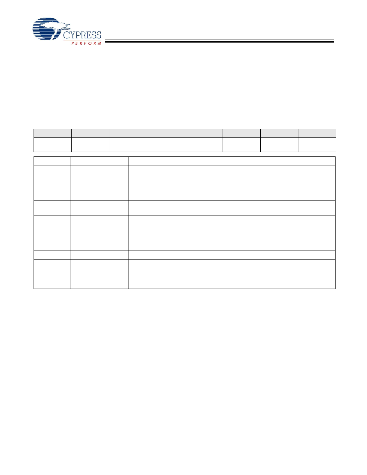
Page 18

SL811HS
Physical Connections
1
2 28
nDACK*
nDRQ*
nWR
D7
D6
D5
D4
Gnd
D3
D2
D1
D0
Gnd
INTR Q
VDD1
nRST
VDD2
Gnd
nCS
DATA-
DATA+
VDD1
CLK/X1
X2
28 PLCC
A0
M/S
171615
14
13
12
11
10
9
8
7
6
5
4
3
25
24
22
21
20
19
18
27
26
23
CM
Figure 4. 28-pin PLCC USB Host/Slave Controller — Pin Layout
These parts are offered in both a 28-pin PLCC package and a 48-pin TQFP package. The 28-pin PLCC packages are the
SL811HS and SL811HS-JCT. The 48-pin TQFP packages is the SL811HST-AXC.
28-Pin PLCC Physical Connections
28-Pin PLCC Pin Layout
*See Table 35 on page 21 for Pin and Signal Description for Pins 2 and 3 in Host Mode.
nRD
28-Pin PLCC Mechanical Dimensions
Document 38-08008 Rev. *D Page 18 of 32
Page 19

SL811HS
The diagram below illustrates a simple +3.3V voltage source.
+3.3 V (VDD)
Sample VDD Generator
3.9v, 1N52288CT-
Figure 5. Sample VDD Generator
Part Number
YYWW-X.X
XXXX
+5V (U SB)
R1
45 Ohms
2N2222
Zener
GND
Package Markings (28-pin PLCC)
YYWW = Date code
XXXX = Product code
X.X = Silicon revision number
Document 38-08008 Rev. *D Page 19 of 32
Page 20

SL811HS
48-Pin TQFP Physical Connections
1
12
13
25
48
37
36
NC
NC
NC
NC
NC
NC
NC
nRD
NC
NC
NC
NC
nWR
nCS
Data+
Clk/X1
nRST
GND
D1
D2
D3
GND
D4
D6
VDD
M/S
A0
nDACK*
NC
nDRQ*
USBGnd
NC
NC
Figure 6. 48-Pin TQFP AXC USB Host/Slave Controller Pin Layout
[4]
48-Pin TQFP AXC Pin Layout
NC
24
NC
CM
VDD1
Data-
NC
48-Pin TQFP
D7
NC
VDD
X2
INTRQ
D0
*See Table 35 on page 21 for Pin and Signal Description for Pins 43 and 44 in Host Mode.
NC
D5
NC
48-Pin TQFP Mechanical Dimensions
Note
4. NC. Indicates No Connection. NC Pins must be left unconnected.
Document 38-08008 Rev. *D Page 20 of 32
Page 21

SL811HS
48/28-Pin USB Host Controller Pins Description
The SL811HST-AXC is packaged in a 48-pin TQFP. The SL811HS and SL811HS-JCT packages are 28-pin PLCC’s. These
devices require a 3.3 VDC power source. The 48-Pin TQFP requires an external 12 or 48 MHz crystal or clock.
Table 35. 48/28-Pin TQFP AXC Pin Assignments and Defi nit ions
48-Pin TQFP
AXC Pin No.
28-Pin PLCC
Pin No.
Pin Type Pin Name Pin Des cription
1 – NC NC No connection.
2 – NC NC No connection.
35 INnWRWrite Strobe Input. An active LOW input used with nCS to write
to registers/data memory.
46 INnCSActive LOW 48-Pin TQFP Chip select. Used with nRD and nWr
when accessing the 48-Pin TQFP.
[5]
5
6 8 VDD1 +3.3 VDC Power for USB Transceivers. V
[6]
7
IN CM Clock Multiply. Select 12 MHz/48 MHz Clock Source.
may be connected to VDD.
DD1
7 9 BIDIR DATA + USB Differential Data Signal HIGH Side.
8 10 BIDIR DATA - USB Differential Data Signal LOW Side.
9 11 GND USB GND Ground Connection for US B.
10 – NC NC No connection.
11 – NC NC No connectio n.
12 – NC NC No connection.
13 – NC NC No connection.
14 – NC NC No connection.
[7]
15
12 VDD +3.3 VDC Device VDD Power.
16 13 IN CLK/X1 Clock or External Crystal X1 connection. The X1/X2 Clock
requires external 12 or 48 MHz matching crystal or clock source.
17 14 OUT X2 External Crystal X2 connection.
18 15 IN nRST Device active low reset input.
19 16 OUT INTRQ Active HIGH Interrupt Request output to external controller.
20 17 GND GND Device Ground.
21 18 BIDIR D0 Data 0. Microprocessor Data/Address Bus.
22 – NC NC No connection.
23 – NC NC No connection.
24 – NC NC No connection.
25 – NC NC No connection.
26 – NC NC No connection.
27 19 BIDIR D1 Data 1. Microprocessor Data/Address Bus.
28 20 BIDIR D2 Data 2. Microprocessor Data/Address Bus.
29 21 BIDIR D3 Data 3. Microprocessor Data/Address Bus.
30 22 GND GND Device Ground.
31 23 BIDIR D4 Data 4. Microprocessor Data/Address Bus.
32 24 BIDIR D5 Data 5. Microprocessor Data/Address Bus.
Notes
5. The CM Clock Multiplier pin must be tied HIGH for a 12 MHz clock source and tied to ground for a 48 MHz clock source.
6. The CM Clock Multiplier pin must be tied HIGH for a 12 MHz clock source a nd tied to ground for a 48 MHz clock source. In 28-pin PL CC’s, this pin is desi gnated
as an ALE input pin.
7. VDD can be derived from the USB supply. See Fig ure 5 on page 19.
Document 38-08008 Rev. *D Page 21 of 32
Page 22

SL811HS
Table 35. 48/28-Pin TQFP AXC Pin Assignments and Defi nit ions (continued)
Notes
8. VDD can be derived from the USB supply. Figure 5 on page 19 shows a simple method to p rovide 3.3V/30 mA. Another opt ion is to use a Torex Semiconductor ,
Ltd. 3.3V SMD regulator (part number XC62HR3302MR).
9. The A0 Address bit is used to access address register or data registers in I/O Mapped or Memory Mapped applications.
48-Pin TQFP
AXC Pin No.
28-Pin PLCC
Pin No.
Pin Type Pin Name Pin Des cription
33 25 BIDIR D6 Data 6. Microprocessor Data/Address Bus.
34 – NC NC No connection.
35 – NC NC No connection.
36 – NC NC No connection.
37 – NC NC No connection.
38 – NC NC No connection.
39 26 BIDIR D7 Data 7. Microprocessor Data/Address Bus.
40 27 IN M/S Master/Slave Mode Select. ’1’ selects Slave. ’0’ = Master.
41 28
[9]
42
[8]
[9]
1
VDD +3.3 VDC Device VDD Power.
IN A0 A0 = ’0’. Selects address pointer. Register A0 = ’1’. Selects data
buffer or register.
43 2 IN nDACK DMA Acknowledge. An active LOW input used to interface to
an external DMA controller. DMA is enabled only in slave mode.
In host mode, the pin should be tied HIGH (logic ’1’).
44 3 OUT nDRQ DMA Request. An active LOW output used with an external
DMA controller. nDRQ and nDACK form the handshake for DMA
data transfers. In host mode, leave the pin unconnected.
45 4 IN nRD Read Strobe Input. An active LOW input used with nCS to read
registers/data memory.
46 – NC NC No connection.
47 – NC NC No connection.
48 – NC NC No connection.
Document 38-08008 Rev. *D Page 22 of 32
Page 23

SL811HS
Package Markings (48-Pin TQFP)
Part Num ber
YYWW -X.X
X XX X
YYWW = Date code
XXXX = Product code
X.X = Silicon revision number
Document 38-08008 Rev. *D Page 23 of 32
Page 24

SL811HS
Electrical Specifications
Notes
10.The 28-PIN plcc can use a 12 MHz Crystal Oscillator or 12 MHz Clock Source.
11.Fundamental mode for 12 MHz Crystal.
12.The SL811HS can use a 12 MHz Clock Source.
Absolute Maximum Ratings
This section lists the absolute maximum ratings of the SL811HS. Stresses above those l isted can cause pe rmanent damag e to
the device. Exposure to maximum rated conditions for extended periods can affect device operation and reliability.
Description Condition
Storage Temperature –40°C to 125°C
Voltage on any pin with respect to ground –0.3V to 6.0V
Power Supply Voltage (V
Power Supply Voltage (V
Lead Temperature (10 seconds) 180°C
Recommended Operating Condition
Parameter Min. Typical Max.
Power Supply Voltage, VDD 3.0V 3.3V 3.45V
Power Supply Voltage, VDD1 3.0V 3.45V
Operating Temperature 0°C 65°C
)4.0V
DD
)4.0V
DD1
Crystal Requirements,
(X1, X2)
Min. Typical Max.
Operating Temperature Range 0°C 65°C
Parallel Resonant Frequency
[10]
48 MHz
Frequency Drift over Temperature ±50 ppm
Accuracy of Adjustment ±30 ppm
Series Resistance 100 Ohms
Shunt Capacitance 3 pF 6 pF
Load Capacitance 20 pF
Drive Level 20 μW 5 mW
Mode of Vibration Third Overtone
[11]
External Clock Input Characteristics (X1)
Parameter Min. Typical Max.
Clock Input Voltage @ X1 (X2 Open) 1.5V
Clock Frequency
[12]
48 MHz
Document 38-08008 Rev. *D Page 24 of 32
Page 25

SL811HS
DC Characteristics
Notes
13.I
CC
measurement includes USB Transceiver curr ent (I
USB
) operating at full speed.
14.I
CCsus1
measured with 12 MHz Clock Input and Internal PLL enabled. Suspend set –(USB transceiver and internal Clocking disabled).
15.I
CCsus2
measured with external Clock, PLL disabled, and Suspend set. For absolute mi nimum current con sumptio n, ensure that all inputs to the device are at
static logic level.
16.All typical values are V
DD
= 3.3V and T
AMB
= 25°C.
17.Z
USBX
impedance values includes an external resistor of 24 Ohms ± 1% (SL811HS revision 1.2 requires external resistor values of 33 Ohms ±1%).
Parameter Description Min. Typ. Max.
V
IL
V
IH
V
OL
V
OH
I
OH
I
OL
I
LL
C
IN
[13]
I
CC
I
CCsus1
I
CCsus2
I
USB
I
USBSUS
[14]
[15]
Input Voltage LOW –0.3V 0.8V
Input Voltage HIGH (5V Tolerant I/O) 2.0V 6.0V
Output Voltage LOW (IOL = 4 mA) 0.4V
Output Voltage HIGH (IOH = –4 mA) 2.4V
Output Current HIGH 4 mA
Output Current LOW 4 mA
Input Leakage ±1 μA
Input Capacitance 10 pF
Supply Current (VDD) inc USB @FS 21 mA 25 mA
Supply Current (VDD) Suspend w/Clk & Pll Enb 4.2 mA 5 mA
Supply Current (VDD) Suspend no Clk & Pll Dis 50 μA 60 μA
Supply Current (V
) 10 mA
DD1
Transceiver Supply Current in Suspend 10 μA
USB Host Transceiver Characteristics
Parameter Description Min. Typ.
V
IHYS
V
USBIH
V
USBIL
V
USBOH
V
USBOL
[17]
Z
USBH
[17]
Z
USBL
I
USB
Every V
capacitor to ensure clean V
DD
at the chip input point (pin) itself.
The best way to do this is to connect a ceramic capacitor
(0.1 μF, 6V) between the pin itself and a good groun d. Keep
Differential
0.2V 200 mV
Input Sensitivity (Data+, Data–)
USB Input Voltage HIGH Driven 2.0V
USB Input Vo l tage LOW 0.8V
USB Output Voltage HIGH 2.0V
USB Output Voltage LOW 0.0V 0.3V
Output Impedance HIGH STATE 36 Ohms 42 Ohms
Output Impedance LOW STATE 36 Ohms 42 Ohms
Transceiver Supply p-p Current (3.3V) 10 mA
pin, including USB VDD, must have a decoupling
(free of high frequency noise)
DD
capacitors with the shortest traces possible (the use of a
ground plane is strongly recommended).
This product was tested as compliant to the USB-IF specification under the test identification number (TID) of 40000 689
and is listed on the USB-IF’s integrators list.
capacitor leads as short as possible. Use surface mount
[16]
Max.
@ FS
Document 38-08008 Rev. *D Page 25 of 32
Page 26

SL811HS
Bus Interface Timing Requirements
nWR
A0
D0-D7
DATA
twr
twahld
twdhld
twasu
twdsu
twdsu
twdhld
I/O W r ite C y c le to Regis te r o r Memory B u ffe r
Register or Memory
A
nCS
twcsu
twshld
Tcscs See Note .
twrhigh
I/O Write Cycle
ddress
Parameter Description Min. Typ. Max.
t
WR
t
WCSU
t
WSHLD
t
WASU
t
WAHLD
t
WDSU
t
WDHLD
t
CSCS
t
WRHIGH
Write pulse width 85 ns
Chip select set-up to nWR LOW 0 ns
Chip select hold time
0 ns
After nWR HIGH
A0 address set-up time 85 ns
A0 address hold time 10 ns
Data to Write HIGH set-up time 85 ns
Data hold time after Write HIGH 5 ns
nCS inactive to nCS* asserted 85 ns
NWR HIGH 85 ns
Note nCS an be held LOW for multiple Write cycles provided nWR is cycled. Write Cycle Time for Auto Inc Mode Writes is 170
ns minimum.
Document 38-08008 Rev. *D Page 26 of 32
Page 27

SL811HS
nRD
A0
D0-D7
DATA
twr
twahld
twdhld
twasu
twdsu
trdhld
I/O Read C y c le from Register or Memory Buffer
Register or Memory
A
trdp
nWR
trshld
trcsu
nCS
tracc
Tcscs *Note
twrrdl
I/O Read Cycle
ddress
Parameter Description Min. Typ. Max.
t
WR
t
RD
t
WCSU
t
WASU
t
WAHLD
t
WDSU
t
WDHLD
t
RACC
t
RDHLD
t
RCSU
t
RSHLD
T
* nCS inactive to nCS *asserted 85 ns
CSCS
t
WRRDL
Write pulse width 85 ns
Read pulse width 85 ns
Chip select set-up to nWR 0 ns
A0 address set-up time 85 ns
A0 address hold time 10 ns
Data to Write HIGH set-up time 85 ns
Data hold time after Write HIGH 5 ns
Data valid after Read LOW 25 ns 85 ns
Data hold after Read HIGH 40 ns
Chip select LOW to Read LOW 0 ns
NCS hold after Read HIGH 0 ns
nWR HIGH to nRD LOW 85ns
Note nCS can be kept LOW during multiple Read cycles provided nRD is cycled. Rd Cycle Time for Auto Inc Mode Reads is 170
ns minimum.
Document 38-08008 Rev. *D Page 27 of 32
Page 28

SL811HS
DMA Write Cycle
nDRQ
nDACK
D0-D7
DATA
nWR
SL811 D M A W R ITE CY CL E TIMING
tdw rp
tdsu
tdack
tdhld
tdw rlo
tackwrh
tdak rq
tac krq
DMA Write Cycle
Parameter Description Min. Typ. Max.
tdack nDACK low 80 ns
tdwrlo nDACK to nWR low delay 5 ns
tdakrq n DACK low to nDRQ high delay 5 ns
tdwrp nWR pulse width 65 ns
tdhld Data hold after nWR high 5 ns
tdsu Data set-up to nWR strobe low 60 ns
tackrq NDACK high to nDRQ low 5 ns
tackwrh NDACK high to nDRQ low 5 ns
twrcycle DMA Write Cycle Time 150 ns
Note nWR must go low after nDACK goes low in order for nDRQ to clear. If this sequence is not implemented as requested, the
next nDRQ is not inserted.
Document 38-08008 Rev. *D Page 28 of 32
Page 29

SL811HS
DMA Read Cycle
nDRQ
nDACK
D0-D7
DATA
nRD
SL811 DM A R EA D CY CL E TIMING
tdrdp
tdaccs
tdack
tdhld
tddrdlo
tdckdr
tdak rq
SL81 1 DMA Read Cycle Timing
nRST
treset
nRD or nWR
tioact
Reset Timing
Parameter Description Min. Typ. Max.
tdack nDACK low 100 ns
tddrdlo nDACK to nRD low delay 0 ns
tdckdr nDACK low to nDRQ high delay 5 ns
tdrdp nRD pulse width 90 ns
tdhld Date hold after nDACK high 5 ns
tddaccs Data access from nDACK low 85 ns
tdrdack nRD high to nDACK high 0 ns
tdakrq nDRQ low after nDACK high 5 ns
trdcycle DMA Read Cycle Time 150 ns
Note Data is held until nDACK goes high regardless of state of nREAD.
Reset Timing
Parameter Description Min. Typ. Max.
t
RESET
t
IOACT
Note Clock is 48 MHz nominal.
Document 38-08008 Rev. *D Page 29 of 32
nRst Pulse width 16 clocks
nRst HIGH to nRD or nWR active 16 clocks
Page 30

SL811HS
Clock Timing Specifications
CLK
CLOCK TIMING
trisetfallthigh
tclk
tlow
Clock Timing
DIMENSIONS IN INCHES
MIN.
MAX.
0.045
0.055
0.026
0.013
0.032
0.021
0.020 MIN.
0.090
0.165
0.120
0.180
0.485
0.495
0.450
0.458
0.458
0.450
0.495
0.485
0.390
0.430
426
1812
11
5
19
25
0.004
SEATING PLANE
1
PIN #1 ID
28-Lead Plastic Leaded Chip Carrier J64
51-85001-*A
Parameter Description Min. Typ. Max.
t
CLK
t
HIGH
t
LOW
t
RISE
t
FALL
Clock Period (48 MHz) 20.0 ns 20.8 ns
Clock HIGH Time 9 ns 11 ns
Clock LOW Time 9 ns 11 ns
Clock Rise Time 5.0 ns
Clock Fall Time 5.0 ns
Clock Duty Cycle 45% 55%
Ordering Information
Part Number Package Type
SL81 1HS 28-pin PLCC –
SL811HS-JCT 28-pin Lead free –
SL81 1HST-AXC 48-pin Lead free –
Package Diagrams
Document 38-08008 Rev. *D Page 30 of 32
Page 31

SL811HS
Package Diagrams (continued)
48-Lead Thin Plastic Quad Flat Pack (7x7x1.4 mm) A48
51-85135-**
Intel is a registered trademark of Intel Corporation. T orex is a trademark of Torex Semiconductors, Ltd. SL811HS is a trademark
of Cypress Semiconductor Corporation. All product and company names mentioned in this document may be the trademarks of
their respective holders.
Document 38-08008 Rev. *D Page 31 of 32
© Cypress Semiconductor Corporation, 2007. The information contained herein is subject to change without notice. Cypress Semiconductor Corporation assumes no responsibility for the use
of any circuitry other than circuitry embodied in a Cypress product. Nor does it convey or imply any license under patent or other rights. Cypress products are not warranted nor intended to be
used for medical, life support, life saving, critical control or safety applications, unless pursuant to an express written agreement with Cypress. Furthermore, Cypress do es not authori ze its
products for use as critical components in life-support systems where a malfunction or failure may reasonably be expected to result in sign ificant injury to the user. The inclusion of Cy press
products in life-support systems application implies that the manufacturer assumes all risk of such use and in doing so indemnifies Cypress against all charges.
Page 32

SL811HS
Document History Page
Document Title: SL811HS Embedded USB Host/Slave Controller
Document Number: 38-08008
REV. ECN NO. Issue Date
** 110850 12/14/01 BHA Converted to Cypress format from ScanLogic
*A 112687 03/22/02 MUL 1) Changed po wer supply voltage to 4.0V in section 7.1
*B 381894 See ECN VCS Went from single column to 2-column format. Combined information from
*C 464641 See ECN ARI Added lead free part numbers to new section Ordering Information and
*D 749518 See ECN ARI Implemented the new template. Changed Figure 4. Labels on pins 2 and 3
Orig. of
Change
Description of Change
2) Changed value of twdsu in section 7.6.2
3) Changed max. power supply voltage to 3.45 V in section 7.2
4) Changed accuracy of adjustment in section 7.2
5) Changed bits 0 and 1 to reserved in section 5.3.8
6) Changed bit 2 to reserved in section 5.3.5 and 5.3.7
7) Changed bit 2 to reserved in section 5.3.1
8) Changed definition of bit 6 in section 5.3.5 & 5.3.7
9) Added section 5.1, Register Values on Power Up and Reset
10) Changed bit description notes in section 5.3.7
11) Changed note about series termination resistors in section 7.5
12) Changed example in section 5.3.9
13) Changed J-K Programming States table in section 5.3.2
14) Added and removed comments for low-power modes in section 5.3.4
15) Removed sections specific to slave operation and SL11H
16) Removed duplicate tables
17) General formatting changes to section headings
18) Fixed all part number references
19) Added comments to section 7.5 and new definitions to section 2.0
SL81 1HS (38-08008) and SL811S/T (83-08009)
corrected references made to these parts. Corrected grammar. Added
compliance statement in section USB Host Transceiver Characteristics.
were swapped; this has been corrected.
Combined the 48-pin TQFP AXC Pin Assignment and Definition table with
the 28-pin PLCC Pin Assignment and Definition table. Removed all instances
of SL811HST-AC. Corrected the variables. Removed references to the
obsolete SL11H.
Document 38-08008 Rev. *D Page 32 of 32
 Loading...