

Page 1
AN204457
How To Use A/D Converter For S6J3110/ S6J3120 Series
Target Products: Refer to Section 2
This application note describes an example of setting for basic A/D Converter function and Range Compare function
in the S6J3110 / S6J3120 Series.
Contents
Series
Product Number (Not Included Package Suffix)
S6J3110
S6J3118, S6J3119, S6J311A, S6J311B, S6J311C, S6J311D, S6J311E
S6J3120
S6J3128, S6J3129, S6J312A
1 Introduction .................................................................. 1
1.1 About This Document ........................................... 1
2 Target Products ........................................................... 1
3 Overview ...................................................................... 2
3.1 A/D Compare Activation ....................................... 2
3.2 A/D Activation Arbitration Functions ..................... 3
3.3 A/D Converter Control Functions .......................... 3
3.4 Configuration ........................................................ 4
3.5 A/D Converter Setting ........................................... 7
4 Registers .................................................................... 20
4.1 Analog Input Control Register (ADER) ............... 20
4.2 A/D Mode Setting Register (ADMD) ................... 20
4.3 A/D Activation Trigger Extended Control Register
(ADTECS) ........................................................... 20
4.4 A/D Activation Trigger Control Status Register
(ADTCS) ............................................................. 21
4.5 A/D Activation Trigger Control Status Clear
Register (ADTCSC)…………………………….21
1 Introduction
1.1 About This Document
This application note is intended for persons who are considering the use of Traveo family S6J3110 / S6J3120 series.
This application note describes an example of setting for basic A/D Converter function and Range Compare function
in the S6J3110 / S6J3120 Series.
4.6 Range Comparison Control Status Register
(ADRCCS)………………………………………. 22
4.7 Upper Threshold Setting Register (ADRCUT) .. 22
4.8 Lower Threshold Setting Register (ADRCLT) ... 22
4.9 A/D Software Activation Channel Selection
Register (ADTSE) ............................................. 23
4.10 A/D Software Activation Register (ADTSS) ....... 23
4.11 A/D Data Register (ADTCD) ............................. 23
4.12 Range Comparison Flag Register (ADRCIF) .... 24
4.13 Range Comparison Flag Clear Register
(ADRCIFC) ....................................................... 24
5 Reference .................................................................. 25
Document History ............................................................ 26
Worldwide Sales and Design Support ............................. 27
Products .......................................................................... 27
PSoC® Solutions ............................................................. 27
Cypress Developer Community....................................... 27
Technical Support ........................................................... 27
2 Target Products
Products of what is described in this operation manual are as follows.
www.cypress.com Document No. 002-04457 Rev. *B 1
Page 2

3 Overview
This section explains an overview of the 12-bit A/D converter.
The 12-bit A/D converter has the function of converting analog input voltage into a 12-bit digital value by RC
successive approximation conversion system. And this section explains the range comparison function. Range
comparison function detects digital value of inside and outside by upper and lower threshold registers settings.
3.1 A/D Compare Activation
The function of A/D activation compare is explained.
3.1.1 Analog Input Control
This A/D converter includes 2 converter units, and can enable or disable each of up to 64 channels of analog input.
3.1.2 Activation Channel
It performs operation for A/D activation request control and A/D conversion data storage with each activation channel.
The A/D activation channel corresponds to each unit of 12-bit A/D converter. The correspondence is as follows.
Activation channels 0-31: 12-bit A/D converter unit 0
Activation channels 32-63: 12-bit A/D converter unit 1
3.1.3 A/D Activation Request
Each activation channel issues an A/D activation request by one of the following methods.
Software
Base timer (Reload timer, PWM timer compare match)
Free-run timer compare match
For software activation, reload timer activation, and PWM timer activation, an arbitrary activation channel can be
selected. For compare match activation, the A/D activation is requested when the value in the free-run timer and the
compare register of each activation channel match.
For an activation request, either single mode or repeat mode can be set for each activation channel. In single
mode, an activation factor causes an activation request. In repeat mode, an activation factor causes a continuous
activation request.
How to Use A/D Converter for S6J3110/ S6J3120 Series
3.1.4 A/D Conversion Data
When A/D conversion is completed, the converted data is stored in the A/D data register. Each activation channel is
equipped with an A/D data register. Each A/D data register contains an error flag bit and error status bit. The status of
the A/D-converted data can be learned from the values of these bits.
3.1.5 Scan Conversion with the A/D Conversion Count Specified
Scan conversion with the A/D conversion count specified can be performed for each activation channel.
1 type of scan conversion with the A/D conversion count specified can be specified for each 12-bit A/D converter unit.
As the specification of an A/D conversion count, a number from 1 to 4 can be selected.
3.1.6 Range Comparison Function
The range comparison can be compared for each activation channel.
Up to 4 types of upper and lower threshold settings can be made. Each activation channel selects 1 combination
from among the 4 types.
Inside or Outside detection can select in the upper and lower thresholds.
Continuous detection count function. (Detection count can select from 1 to 7.)
3.1.7 Interrupt Request
Each activation channel can generate an interrupt request when the A/D conversion is completed.
3.1.8 Data Protection Function
For each A/D data register, the data protection function can be set. The protection function is effective for factors that
are not compare match activation. When the data protection function is enabled, the A/D activation request is masked
until data is read from the A/D data register and the interrupt flag is cleared.
www.cypress.com Document No. 002-04457 Rev. *B 2
Page 3

3.1.9 Failure Diagnosis Function
The 12-bit A/D converter has a failure diagnosis function. The AVRH and AVRL voltage conversion diagnosis.
This product has the function of fixing the input voltage level of the internal A/D converter to the AVRH or AVRL level
and perform A/D conversion.
3.2 A/D Activation Arbitration Functions
The A/D activation arbitration for each 12-bit A/D converter unit.
The A/D activation arbitration consists of the arbitration circuit, A/D activation trigger generation, and analog
channel number selection.
The A/D activation arbitration arbitrates an activation request from the A/D activation compare and generates
the activation trigger, A/D conversion cancellation signal, and analog channel number.
The A/D activation arbitration selects one from among the activation requests from different A/D activation
compares to generate the activation trigger. The A/D activation arbitration performs priority control when
activation requests from different A/D activation compares conflict with each other.
The priority orders are determined according to the following rules.
When an activation factor with the same priority order occurs while A/D conversion is stopped:
The activation factor with the smaller activation channel number is processed first.
When an activation factor with a different priority order occurs while A/D conversion is stopped:
The activation factor with the higher priority order is processed first.
When an activation factor with a higher priority order occurs while A/D conversion is in progress:
The current conversion is interrupted, and the activation factor with the higher priority order is processed.
Arbitration is performed again after this conversion, and then the processing of the interrupted activation factor
is restarted.
When an activation factor with a lower priority order occurs while A/D conversion is in progress:
Arbitration is again performed after the current conversion is completed, and then the activation factor with the
lower priority order is processed.
When an activation factor with the same priority order occurs while A/D conversion is in progress:
Arbitration is again performed after the current conversion is completed, and then the activation factor with the
same priority order is processed.
How to Use A/D Converter for S6J3110/ S6J3120 Series
3.3 A/D Converter Control Functions
This section explains the functions of the 12-bit A/D converter control. A function for A/D-converting the analog
voltage that is input to the analog input pin (input voltage) into a digital value is supported and it has the following
features.
The conversion system used is an RC successive approximation conversion system with a sample hold circuit.
The analog input pin can be selected by the registers (make its setting in the A/D activation compare block).
1 sequence of A/D conversion is performed in response to 1 activation factor.
If another activation signal is input during A/D conversion, reactivation is performed. (Reactivation function)
If the A/D conversion cancellation signal is received during A/D conversion, the current processing is stopped and
initialized. (Forcible stop function)
For setting the sampling time, the sampling time setting that is common to all the channels or sampling time
setting for each channel can be selected.
www.cypress.com Document No. 002-04457 Rev. *B 3
Page 4
3.4 Configuration
This section shows the configuration of the 12-bit A/D converter.
3.4.1 Configuration of the A/D Activation Compare
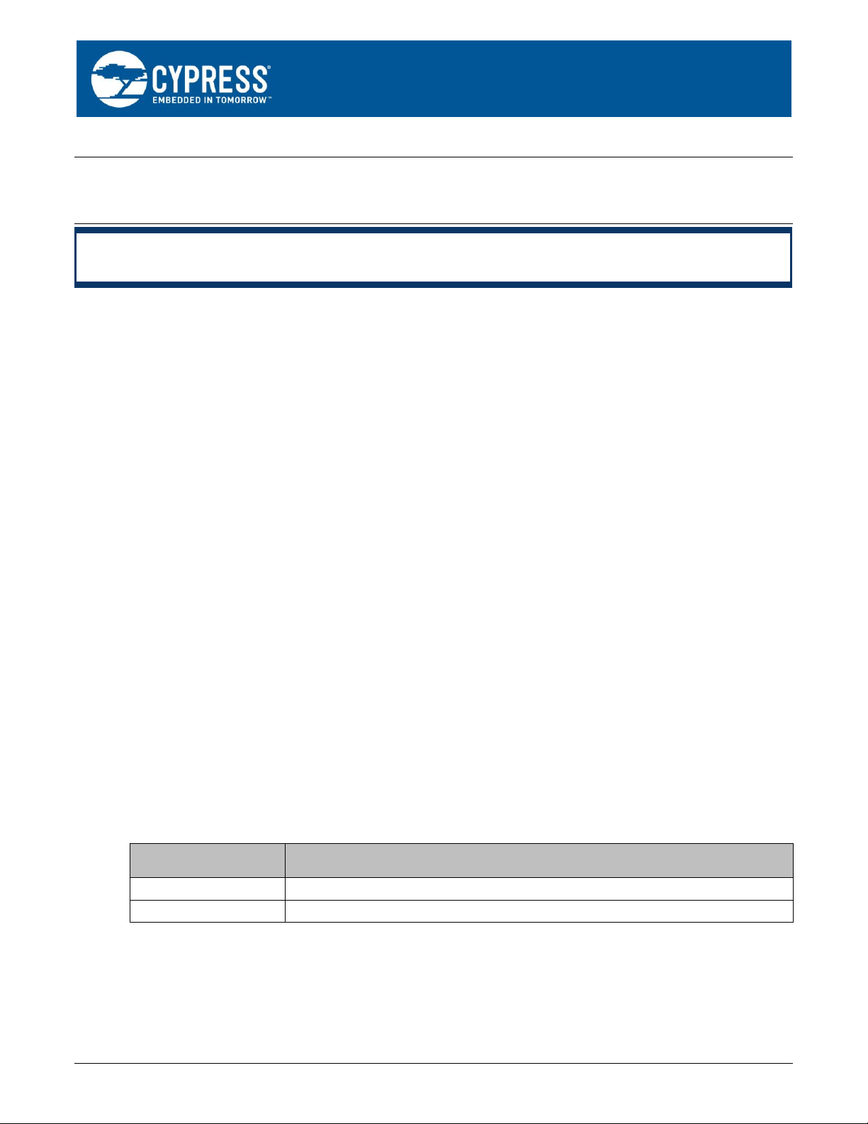
The configuration of the A/D activation compares shows in the following.
Figure 1. Configuration of the A/D Activation Compare (n=31, A/D Converter Unit 0)
How to Use A/D Converter for S6J3110/ S6J3120 Series
www.cypress.com Document No. 002-04457 Rev. *B 4
Page 5
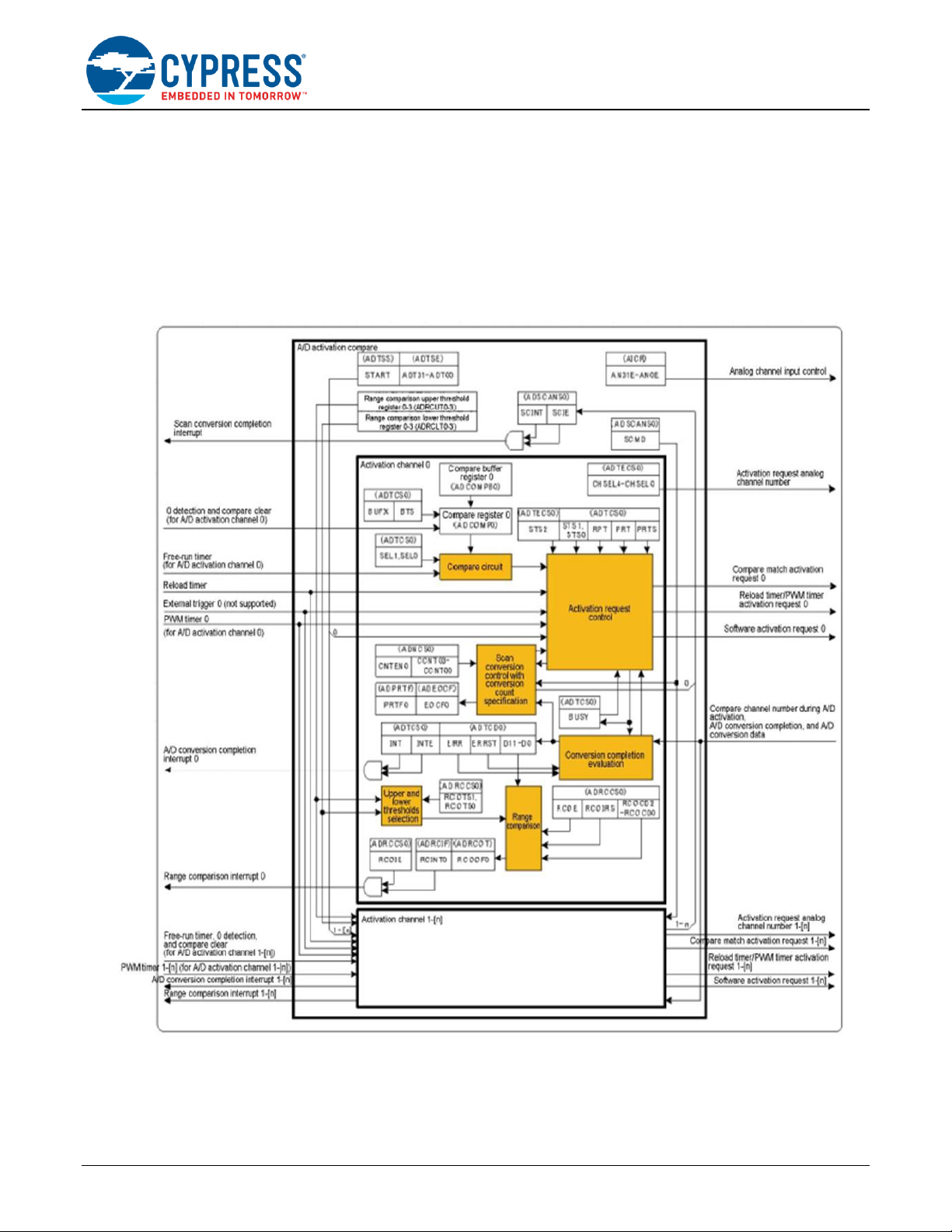
3.4.2 Configuration of the A/D Activation Arbitration
The configuration of the A/D activation arbitration shows in the following.
Figure 2. Configuration of the A/D Activation Arbitration
How to Use A/D Converter for S6J3110/ S6J3120 Series
www.cypress.com Document No. 002-04457 Rev. *B 5
Page 6
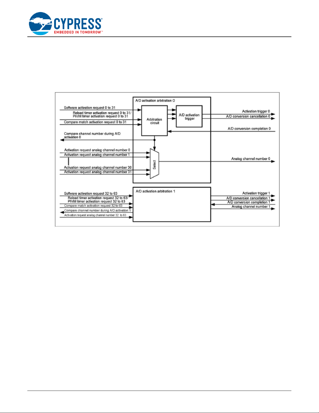
3.4.3 Configuration of the 12-Bit A/D Converter Control
The configuration of the A/D Converter Control shows in the following.
Figure 3. Configuration of the 12-Bit A/D Converter Control (n=32, A/D Converter Unit 0)
How to Use A/D Converter for S6J3110/ S6J3120 Series
www.cypress.com Document No. 002-04457 Rev. *B 6
Page 7

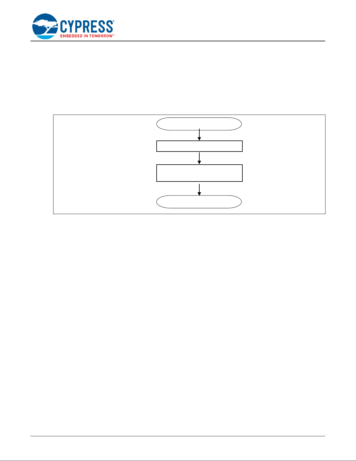
A/D Converter time setting
Activation channel and factor
setting
Range comparison function
setting
A/D Converter Start setting
End
Analog input enable setting
A/D Converter setting start
- A/D Converter end interrupt setting
-Range Comparison interrupt setting
Interrupt setting
End
3.5 A/D Converter Setting
3.5.1 Example of Settings
Example of the A/D Converter setting flow shows in the following. And setting items shows in the Figure4.
How to Use A/D Converter for S6J3110/ S6J3120 Series
Figure 4. A/D Converter Function Example of Settings
www.cypress.com Document No. 002-04457 Rev. *B 7
Page 8
Table 1. A/D Converter Function Example of Setting Items
Setting item
Setting value
Analog input pin
AN14
Sampling time
1.3µs
Compare time
0.8µs
Activation channel
Channel 0
Activation factor
Software
A/D Converter mode
Repeat conversion
A/D Converter protection
Disable
A/D Conversion Completion interrupt
Enable
A/D Range Comparison function
Enable
A/D Range Comparison interrupt
Enable
Each item (Figure 4) of the setting flow describes in the following.
How to Use A/D Converter for S6J3110/ S6J3120 Series
www.cypress.com Document No. 002-04457 Rev. *B 8
Page 9
Analog input pin setting (AN14)
ADER_ADER0=0x00004000
ADER register key code setting
Analog inputs enable setting
End
3.5.1.1 Analog Input Enable Setting The analog input enable setting uses Analog Input Control Register (ADER). This register is target of the Key Code
Register. (Please refer to the "4.1.1.Key Code Register" of the “CHAPTER: 12 Bit-A/D Converter” in the S6J3110 /
S6J3120 Series Hardware Manual.) This application note setting is AN14 in the analog input pin.
How to Use A/D Converter for S6J3110/ S6J3120 Series
Figure 5. Analog Input Enable Setting Flow
www.cypress.com Document No. 002-04457 Rev. *B 9
Page 10

3.5.1.2 A/D Converter Time Setting
Sampling time setting
(48 peripheral clock cycles:1.3µs* )
ADC0_ADMD0_ST=3
Common sampling time setting to all channels
ADC0_ADMD0_STPCEN=0
A/D Converter time setting
End
Compare time setting
(28 peripheral clock cycles:0.8µs* )
ADC0_ADMD0_CT=0
The A/D converter time setting uses A/D Mode Setting Register. (ADMD) The A/D Converter time setting depends on
Compare time and Sampling time. And this register selects whether to set sampling time for A/D conversion for each
channel or to set a common setting.
How to Use A/D Converter for S6J3110/ S6J3120 Series
Figure 6. A/D Converter Time Setting Flow
Note: * When the peripheral clock is 36MHz operation on S6J311E.
www.cypress.com Document No. 002-04457 Rev. *B 10
Page 11

3.5.1.3 Activation Channel and Factor Setting
The activation channel setting uses A/D Activation Trigger Extended Control Register (ADTECS). The activation
factor setting uses A/D Activation Trigger Control Status Register (ADTCS) and ADTECS.
The Interrupt Request Enable Bit sets disable. The Repeat Conversion Selection Bit sets repeat conversion. The A/D
Data Register Protection Enable Bit sets disable. These settings are in the ADTCS register.
The Activation channel and factor settings flow shows in the following.
Figure 7. A/D Converter Activation Channel and Factor Setting Flow
How to Use A/D Converter for S6J3110/ S6J3120 Series
www.cypress.com Document No. 002-04457 Rev. *B 11
Page 12

How to Use A/D Converter for S6J3110/ S6J3120 Series
void AD_Init(void)
{
// KEYCode Register
ADER_KEYCDR=0x20000804;
ADER_KEYCDR=0x60000804;
ADER_KEYCDR=0xA0000804;
ADER_KEYCDR=0xE0000804;
ADER_ADER0=0x00004000;//Analog input (AN14)
//All Channel Sampling time common
ADC0_ADMD0_STPCEN=0;
//Sampling time setting
ADC0_ADMD0_ST=3;
//Compare time setting
ADC0_ADMD0_CT=0;
// A/D Activation Trigger Extended Control Resgister
// Analog Channel select
ADC0_ADTECS0_CHSEL=14;
// Activation factor setting (Software trigger)
ADC0_ADTCS0_STS=0;
ADC0_ADTECS0_STS2=0;
// A/D Interrupt request disable
ADC0_ADTCS0_INTE=0;
//Repeat conversion
ADC0_ADTCS0_RPT=1;
// A/D data register protection disable
ADC0_ADTCS0_PRT=0;
}
←Analog input enable setting
←Sampling time setting
←Compare time setting
←Sampling time setting common to all
channels
←Activation channel selection
←A/D activation factor setting
←A/D Interrupt request disable
←Repeat conversion mode setting
←A/D data register protection disable
The sample program shows in the following.
Figure 8. Setting Program from Analog Input to Activation Factor Setting
www.cypress.com Document No. 002-04457 Rev. *B 12
Page 13

Upper and Lower threshold setting
-Upper Threshold Setting
ADRCUT0: C [11-0] =0x800
-Lower Threshold Setting
ADRCLT0: C [11-0] =0x555
Inside/outside-Range Check Selection
ADRCCS0: RCOIRS=1
Range Comparison Interrupt Request Enable
ADRCCS0: RCOIE=1
Continuous Detection Count Specification setting
ADRCCS0: RCOCD [2-0] =1
End
Range comparison function setting
Range Comparison Execution Enable setting
ADRCCS0: RCOE=1
Upper and Lower Threshold Selection
ADRCCS0: RCOTS [1-0] =1
3.5.1.4 Range Comparison Function Setting
The Range Comparison setting uses Range Comparison Control Status Register (ADRCCS).
The ADRCCS Register select range comparison execution enables upper/lower threshold selection, inside/outside-
range checking, interrupt request and continuous detection count.
Upper and lower threshold values set Upper/Lower Threshold Setting Register (ADRCUT/ADRCLT).
(Please refer to the” P18 Appendix: About the Range Comparison Operation”.)
The range comparison function setting flow shows in the following
Figure 9. Range Comparison Function Setting Flow
How to Use A/D Converter for S6J3110/ S6J3120 Series
www.cypress.com Document No. 002-04457 Rev. *B 13
Page 14

How to Use A/D Converter for S6J3110/ S6J3120 Series
void AD_RangeCompare(void)
{
// A/D Range comparison execution enable
ADC0_ADRCCS0_RCOE=1;
// A/D Upper threshold setting
ADC0_ADRCUT0_C=0x800;
// A/D Lower threshold setting
ADC0_ADRCLT0_C=0x555;
// A/D Upper and Lower threshold (ADRCUT0/ADRCLT0)
ADC0_ADRCCS0_RCOTS=0;
// A/D Inside check setting
ADC0_ADRCCS0_RCOIRS=1;
// A/D Range comparison interrupt request enable
ADC0_ADRCCS0_RCOIE=1;
// A/D Continue detection count(1)
ADC0_ADRCCS0_RCOCD=1;
}
←Range Comparison Execution
Enable setting
←Upper Threshold Setting
←Lower Threshold Setting
←Upper and Lower
Threshold Selection
←Inside/outside-Range Check Selection
←Range Comparison Interrupt
Request Enable
←Continuous Detection Count Specification setting
The sample program shows in the following.
Figure 10. A/D Range Comparison Function Setting Program
3.5.1.5 A/D Converter Start Setting
The A/D Converter start sets software activation channel selection in the A/D Software Activation Channel Selection
Register (ADTSE). And, the Interrupt request enables bit sets in the A/D Activation Trigger Control Status Register
(ADTCS). Then, the A/D converter function activates by the START bit in the A/D Software Activation Register
(ADTSS).
The A/D converter start setting flow shows in the following.
www.cypress.com Document No. 002-04457 Rev. *B 14
Page 15

How to Use A/D Converter for S6J3110/ S6J3120 Series
End
A/D software activation channel enable setting
ADTSE0:ADT0=1
A/D Converter Interrupt Request enables
setting
ADTCS0: INTE=1
A/D Converter activation
ADTSS0: START=1
A/D Converter Start
setting
void AD_Start(void)
{
// A/D software activation channel enable
ADC0_ADTSE0_ADT0=1;
// A/D Interrupt request enable
ADC0_ADTCS0_INTE=1;
// A/D conversion activation
ADC0_ADTSS0_START=1;
}
←A/D software activation channel
enable setting
←A/D Converter activation
←A/D Interrupt Request enables setting
Figure 11. A/D Converter Start Setting Flow
The sample program shows in the following.
www.cypress.com Document No. 002-04457 Rev. *B 15
Figure 12. A/D Converter Start Setting Program
Page 16

// A/D Converter end interrupt routine
FN_IRQ_DEFINE_BEGIN(Adc_Isr_Adc0_EndOfConversion, INTERRUPTS_IRQ_NUMBER_396)
{
// A/D data get
AD_data=ADC0_ADTCD0_D;
// A/D interrupt request flag clear
ADC0_ADTCSC0_INTC=1;
}
FN_IRQ_DEFINE_END()
←A/D Conversion Data read
←A/D Converter interrupt request flag clear
3.5.1.6 Interrupt Routine Setting The interrupt routine can set in the A/D converter end and range comparison process.
The A/D converter end interrupt routine is generated by the A/D conversion completion.
This interrupt routine read A/D conversion data in the A/D Data Register (ADTCD). And, the A/D Activation Trigger
Control Status Clear Register (ADTCSC) clear the A/D converter interrupt request flag.
The A/D converter Interrupt setting flow shows in the following.
How to Use A/D Converter for S6J3110/ S6J3120 Series
Figure 13. A/D Converter End Interrupt Routine Setting Flow
The sample program shows in the following.
Figure 14. A/D Converter End Interrupt Routine Setting Program
www.cypress.com Document No. 002-04457 Rev. *B 16
Page 17

How to Use A/D Converter for S6J3110/ S6J3120 Series
Range comparison interrupt factor flag
clear
ADRCIFC0:RCINTC0=1
End
Range Comparison interrupt routine
// A/D Range compare detection interrupt routine
FN_IRQ_DEFINE_BEGIN(Adc_Isr_Adc0_RangeCompare, INTERRUPTS_IRQ_NUMBER_397)
{
// A/D Range comparison interrupt factor flag clear
ADC0_ADRCIFC0_RCINTC0=1;
}
FN_IRQ_DEFINE_END()
←Range comparison interrupt factor flag
clear
Then, the range comparison interrupts routine setting flow shows in the following
The Range comparison interrupt routine is generated by the detection in the range. Range comparison interrupt
factor flag clear by the RCINTC bit in the Range Comparison Flag Clear Register (ADRCIFC).
Figure 15. Range Comparison Interrupt Routine Setting Flow
The sample program shows in the following.
Figure 16. Range Comparison Interrupt Routine Setting Program
www.cypress.com Document No. 002-04457 Rev. *B 17
Page 18

Appendix:
-About the Range Comparison Operation
Range comparison is performed when range comparison is enabled (ADRCCS.RCOE="1"), A/D conversion ends,
and then data is stored in the A/D data bits (ADTCD.D11 to D0).
Range comparison compares the upper and lower threshold setting registers (ADRCUT/ADRCLT) selected by the
upper and lower threshold selection bits for range comparison (ADRCCS.RCOTS1, RCOTS0) with the A/D data bits
(ADTCD.D11 to D0).
The A/D Range comparison detection shows in the following Figure17.
-A/D conversion result “1”, “4”,”5” are detected by setting of the inside range threshold.
-A/D conversion result “2”, “3”,”6” are detected by setting of the outside range threshold.
These detection operations show Table2 in the following.
How to Use A/D Converter for S6J3110/ S6J3120 Series
Figure 17. Range Comparison Operation
www.cypress.com Document No. 002-04457 Rev. *B 18
Page 19

Table 2 . Selection for Upper and Lower Thresholds
How to Use A/D Converter for S6J3110/ S6J3120 Series
The range comparison function equips continuous detection function for range comparison result.
The continuous detection function performs continuous detection of range comparison result and reduces noise.
When as many detection states of range comparison result as the count set by the continuous detection count
specification for range comparison (ADRCCS.RCOCD2 to RCOCD0) are continuously detected, the range
comparison interrupt factor flag bit (ADRCIF.RCINT) is set to "1". If range comparison result comes to be "not
detected" even once during continuous detection, the continuous detection measurement is cleared to 0 times and
the measurement is performed again.
www.cypress.com Document No. 002-04457 Rev. *B 19
Page 20

4 Registers
Bit
Bit name
Description
Setting register
Value
Contents
31-0
ADE[31-0]
Analog Input Enable Bits
1 (*)
Enable
Bit
Bit name
Description
Setting register
Value
Contents
7
STPCEN
Sampling Time Setting per Channel Enable Bit
0
Sampling time
setting common to all
channels
6-4
Reserved
Reserved
0
-
3-2
CT[1-0]
Compare Time Setting Bits
0
28 peripheral clock
cycles
1-0
ST[1-0]
Sampling Time Setting Bits
3
48 peripheral clock
cycles
Bit
Bit name
Description
Setting register
Value
Contents
15-9
Reserved
Reserved
0
-
8
STS2
A/D activation Factor Selection Bits
0
Software activation
7-5
Reserved
Reserved
0
-
4-0
CHSEL[4-0]
Analog Channel Selection Bits
14
Channel 14
This section shows the registers of the A/D converter in the example of settings.
4.1 Analog Input Control Register (ADER)
The Analog Input Control Register (ADER) control analog input. This register is target of the Key Code Register.
(Please refer to the "4.1.1.Key Code Register" of the “CHAPTER: 12 Bit-A/D Converter” in the S6J3110 / S6J3120
Series Hardware Manual.)
Table 3. Analog Input Control Register Example of Settings
Note: *When an Analog input selects AN14, Analog Input Enable Bit is “ADE14=1” setting.
4.2 A/D Mode Setting Register (ADMD)
The A/D Mode Setting Register (ADMD) sets the function of setting the compare time and sampling time for A/D
conversion.
Table 4. A/D Mode Setting Register Example of Settings
How to Use A/D Converter for S6J3110/ S6J3120 Series
4.3 A/D Activation Trigger Extended Control Register (ADTECS)
The A/D Activation Trigger Extended Control Register (ADTECS) selects the activation factor and analog Input
channel.
Table 5. A/D Activation Trigger Extended Control Register Example of Settings
www.cypress.com Document No. 002-04457 Rev. *B 20
Page 21

How to Use A/D Converter for S6J3110/ S6J3120 Series
Bit
Bit name
Description
Setting register
Value
Contents
15
BUSY
A/D activation Request in Progress Bit
0
A/D activation has not been
requested
14
INT
Interrupt Request Flag Bit
0
A/D conversion has not been
completed
13
INTE
Interrupt Request Enable Bit
1
Enable interrupt request output.
12-11
STS[1-0]
A/D activation Factor Selection Bits
0
Software activation
10
RPT
Repeat Conversion Selection Bit
1
Repeat conversion
9
PRT
A/D Data Register Protection Enable Bit
0
Protection disabled
8
PRTS
A/D Data Register Protection Release Selection
Bit
0
Data reading and interrupt flag
clear
7-6
SEL[1-0]
Count Direction Selection Bits
0
Both up/down count
5
BUFX
Compare Register Buffer Function Control Bit
1
Disabled
4
BTS
Compare Register Buffer Transfer Control Bit
0
When the “BUFX” is disabled,
this bit is disabling.
3-0
Reserved
Reserved
0
-
Bit
Bit name
Description
Setting register
Value
Contents
15
BUSYC
BUSY Clear Bit
1
Clear the ADTCS
Register BUSY bit.
14
INTC
INT Clear Bit
1
Clear the ADTCS
Register INT bit.
13-0
Reserved
Reserved
0
-
4.4 A/D Activation Trigger Control Status Register (ADTCS)
The A/D Activation Trigger Control Status Register (ADTCS) is used for A/D activation request confirmation,
permission/prohibition of interrupt request, confirmation of interrupt request status, selection of activation factor,
selection of conversion mode, control of protection function, selection of the compare value used for compare
operation, buffer control of the compare value and selection of an analog input channel.
Table 6. A/D Activation Trigger Control Status Register Example of Settings
Note: -BUSY, INT, PRTS, SEL, BUFX, BTS bits are initial values in this APPLICATION NOTE.
4.5 A/D Activation Trigger Control Status Clear Register (ADTCSC)
The A/D Activation Trigger Control Status Clear Register (ADTCSC) clears the bits in the A/D activation trigger
control status register (ADTCS).
Table 7. A/D Activation Trigger Control Status Clear Register Example of Settings
www.cypress.com Document No. 002-04457 Rev. *B 21
Page 22

How to Use A/D Converter for S6J3110/ S6J3120 Series
Bit
Bit name
Description
Setting register
Value
Contents
7-5
RCOCD[2-0]
Continuous Detection Count Specification
Bits
1
Set the continuous
detection count to 1
4
RCOIRS
Inside/outside-Range Check Selection Bit
1
Inside range
3
RCOIE
Range Comparison Interrupt Request
Enable Bit
1
Range comparison
interrupt enabled
2
RCOE
Range Comparison Execution Enable Bit
1
Range comparison
execution enabled
1-0
RCOTS[1-0]
Upper and Lower Threshold Selection Bits
0
Upper Threshold register
0/Lower Threshold
register0
Bit
Bit name
Description
Setting register
Value
Contents
15-12
Reserved
Reserved
0
-
11-0
C[11-0]
Upper Threshold Bits
0x800 (*)
Upper Threshold
Bit
Bit name
Description
Setting register
Value
Contents
15-12
Reserved
Reserved
0
-
11-0
C[11-0]
Lower Threshold Bits
0x555 (*)
Lower Threshold
4.6 Range Comparison Control Status Register (ADRCCS)
The Range Comparison Control Status Register (ADRCCS) performs continuous detection count instructions,
inside/outside-range check selection, range comparison interrupt request permission/prohibition, range comparison
execution permission/prohibition and upper and lower threshold selection.
Table 8. Range Comparison Control Status Register Example of Settings
4.7 Upper Threshold Setting Register (ADRCUT)
The Upper Threshold Setting Register (ADRCUT) sets the upper threshold to be used to compare ranges.
Table 9. Upper Threshold Setting Register Example of Settings
Note: *This upper threshold value is example.
4.8 Lower Threshold Setting Register (ADRCLT)
The Lower Threshold Setting Register (ADRCLT) sets the lower threshold to be used to compare ranges.
Table 10. Lower Threshold Setting Register Example of Settings
Note: *This lower threshold value is example.
www.cypress.com Document No. 002-04457 Rev. *B 22
Page 23

How to Use A/D Converter for S6J3110/ S6J3120 Series
Bit
Bit name
Description
Setting register
Value
Contents
31-0
ADT[31-0]
Software activation Channel Selection Bits
1
Enable software activation.
Bit
Bit name
Description
Setting register
Value
Contents
7-1
Reserved
Reserved
0
-
0
START
A/D Conversion activation Bit (Software)
1
Activate the A/D conversion
function.
Bit
Bit name
Description
Setting register
Value
Contents
15
ERR
Conversion Data Error Flag Bit
0,1
The conversion data are
normal (0) or not normal (1).
14
ERRST
Conversion Data Error Status Bit
(Only if ERR=1)
0,1
The conversion data are old
results (0) or new data (1)
by overwritten.
13-12
Reserved
Reserved
-
-
11-0
D[11-0]
A/D Data Bits
0-0xFFF
Conversion data
4.9 A/D Software Activation Channel Selection Register (ADTSE)
The A/D Software Activation Channel Selection Register (ADTSE) selects the activation channel to issue the A/D
activation request.
Table 11. A/D Software Activation Channel Selection Register Example of Settings
4.10 A/D Software Activation Register (ADTSS)
The A/D Software Activation Register(ADTSS) is set to generate the A/D conversion start request. The activation
channel is specified by the A/D software activation channel selection register (ADTSE).
Table 12 A/D Software Activation Register Example of Settings
4.11 A/D Data Register (ADTCD)
The A/D Data Register (ADTCD) stores the A/D conversion results.
Table 13. A/D Data Register Example of Settings
Note: These ERR, ERRST, D [11-0] bit are read-only.
www.cypress.com Document No. 002-04457 Rev. *B 23
Page 24

Bit
Bit name
Description
Setting register
Value
Contents
31-0
RCINT[31-0]
Conversion Data Error Flag Bits
0,1
Range comparison interrupt
factor are clear (0) or
generation status (1).
Bit
Bit name
Description
Setting register
Value
Contents
31-0
RCINTC[31-0]
RCINT Clear Bits
1
Clear the ADRCIF
Register RCINT bit
4.12 Range Comparison Flag Register (ADRCIF)
The Range Comparison Flag Register (ADRCIF) shows interrupt factors for continuous detection of range
comparison results.
Table 14. Range Comparison Flag Register Example of Settings
Note: The RCINT bit is read-only. The RCINT bit is cleared to "0" by writing "1" in the ADRCIFC Register RCINTC bit.
4.13 Range Comparison Flag Clear Register (ADRCIFC)
The Range Comparison Flag Clear Register (ADRCIFC) clears the bits in the range comparison flag register.
Table 15. Range Comparison Flag Clear Register Example of Settings
How to Use A/D Converter for S6J3110/ S6J3120 Series
www.cypress.com Document No. 002-04457 Rev. *B 24
Page 25

5 Reference
[1]. 32-BIT MICROCONTROLLER Cypress Traveo Family S6J3110 series HARDWARE MANUAL
[2]. 32-BIT MICROCONTROLLER Cypress Traveo Family S6J3120 series HARDWARE MANUAL
How to Use A/D Converter for S6J3110/ S6J3120 Series
www.cypress.com Document No. 002-04457 Rev. *B 25
Page 26

How to Use A/D Converter for S6J3110/ S6J3120 Series
Revision
ECN
Orig. of
Change
Submission
Date
Description of Change
** KHAS
07/31/2015
Initial release
*A
5058934
KHAS
03/15/2016
Converted Spansion Application Note “S6J3110_AN708-00015” to Cypress
format
*B
5876001
AESATMP8
09/07/2017
Updated logo and Copyright.
Document History
Document Title: AN204457 - How to Use A/D Converter for S6J3110/ S6J3120 Series
Document Number: 002-04457
www.cypress.com Document No. 002-04457 Rev. *B 26
Page 27

How to Use A/D Converter for S6J3110/ S6J3120 Series
ARM® Cortex® Microcontrollers
cypress.com/arm
Automotive
cypress.com/automotive
Clocks & Buffers
cypress.com/clocks
Interface
cypress.com/interface
Internet of Things
cypress.com/iot
Memory
cypress.com/memory
Microcontrollers
cypress.com/mcu
PSoC
cypress.com/psoc
Power Management ICs
cypress.com/pmic
Touch Sensing
cypress.com/touch
USB Controllers
cypress.com/usb
Wireless Connectivity
cypress.com/wireless
Worldwide Sales and Design Support
Cypress maintains a worldwide network of offices, solution centers, manufacturer’s representatives, and distributors. To find
the office closest to you, visit us at Cypress Locations.
Products
PSoC® Solutions
PSoC 1 | PSoC 3 | PSoC 4 | PSoC 5LP | PSoC 6
Cypress Developer Community
Forums | WICED IOT Forums | Projects | Videos | Blogs |
Training | Components
Technical Support
cypress.com/support
All other trademarks or registered trademarks referenced herein are the property of their respective owners.
© Cypress Semiconductor Corporation, 2015-2017. This document is the property of Cypress Semiconductor Corporation and its subsidiaries, including
Spansion LLC (“Cypress”). This document, including any software or firmware included or referenced in this document (“Software”), is owned by
Cypress under the intellectual property laws and treaties of the United States and other countries worldwide. Cypress reserves all rights under such
laws and treaties and does not, except as specifically stated in this paragraph, grant any license under its patents, copyrights, trademarks, or other
intellectual property rights. If the Software is not accompanied by a license agreement and you do not otherwise have a written agreement with
Cypress governing the use of the Software, then Cypress hereby grants you a personal, non-exclusive, nontransferable license (without the right to
sublicense) (1) under its copyright rights in the Software (a) for Software provided in source code form, to modify and reproduce the Software solely for
use with Cypress hardware products, only internally within your organization, and (b) to distribute the Software in binary code form externally to end
users (either directly or indirectly through resellers and distributors), solely for use on Cypress hardware product units, and (2) under those claims of
Cypress’s patents that are infringed by the Software (as provided by Cypress, unmodified) to make, use, distribute, and import the Software solely for
use with Cypress hardware products. Any other use, reproduction, modification, translation, or compilation of the Software is prohibited.
TO THE EXTENT PERMITTED BY APPLICABLE LAW, CYPRESS MAKES NO WARRANTY OF ANY KIND, EXPRESS OR IMPLIED, WITH REGARD
TO THIS DOCUMENT OR ANY SOFTWARE OR ACCOMPANYING HARDWARE, INCLUDING, BUT NOT LIMITED TO, THE IMPLIED WARRANTIES
OF MERCHANTABILITY AND FITNESS FOR A PARTICULAR PURPOSE. To the extent permitted by applicable law, Cypress reserves the right to
make changes to this document without further notice. Cypress does not assume any liability arising out of the application or use of any product or
circuit described in this document. Any information provided in this document, including any sample design information or programming code, is
provided only for reference purposes. It is the responsibility of the user of this document to properly design, program, and test the functionality and
safety of any application made of this information and any resulting product. Cypress products are not designed, intended, or authorized for use as
critical components in systems designed or intended for the operation of weapons, weapons systems, nuclear installations, life-support devices or
systems, other medical devices or systems (including resuscitation equipment and surgical implants), pollution control or hazardous substances
management, or other uses where the failure of the device or system could cause personal injury, death, or property damage (“ Unintended Uses”). A
critical component is any component of a device or system whose failure to perform can be reasonably expected to cause the failure of the device or
system, or to affect its safety or effectiveness. Cypress is not liable, in whole or in part, and you shall and hereby do release Cypress from any claim,
damage, or other liability arising from or related to all Unintended Uses of Cypress products. You shall indemnify and hold Cypress harmless from and
against all claims, costs, damages, and other liabilities, including claims for personal injury or death, arising from or related to any Unintended Uses of
Cypress products.
Cypress, the Cypress logo, Spansion, the Spansion logo, and combinations thereof, WICED, PSoC, CapSense, EZ-USB, F-RAM, and Traveo are
trademarks or registered trademarks of Cypress in the United States and other countries. For a more complete list of Cypress trademarks, visit
cypress.com. Other names and brands may be claimed as property of their respective owners.
www.cypress.com Document No. 002-04457 Rev. *B 27
 Loading...