

Page 1
S29VS256R
S29VS128R
S29XS256R
S29XS128R
256/128-Mbit (32/16 Mbyte), 1.8 V, 16-bit
Data Bus, Multiplexed MirrorBit
®
Flash
Features
Single 1.8 V supply for read/program/erase (1.70–1.95 V)
65nm MirrorBit® Technology
Address and Data Interface Options
– Address and Data Multiplexed for reduced I/O count
(ADM) S29VS-R
– Address-High, Address-Low, Data Multiplexed for minimum
I/O count (AADM) S29XS-R
Simultaneous Read/Write operation
32-word Write Buffer
Bank architecture
– Eight-bank
Four 32-KB sectors at the top or bottom of memory array
255/127 of 128-KB sectors
Programmable linear (8/16-word) with wrap around and
continuous burst read modes
Secured Silicon Sector region consisting of 128 words each
for factory and customer
10-year data retention (typical)
Cycling Endurance: 100,000 cycles per sector (typical)
RDY output indicates data available to system
Command set compatible with JEDEC (42.4) standard
Hardware sector protection via V
Handshaking by monitoring RDY
Offered Packages
– 44-ball FBGA (6.2 mm 7.7 mm 1.0 mm)
Low V
Write operation status bits indicate program and erase
operation completion
Suspend and Resume commands for Program and Erase
operations
Asynchronous program operation, independent of burst
control register settings
V
Support for Common Flash Interface (CFI)
write inhibit
CC
input pin to reduce factory programming time
PP
PP
pin
General Description
The Cypress S29VS256/128R and S29XS256/128R are MirrorBit® Flash products fabricated on 65nm process technology. These
burst mode Flash devices are capable of performing simultaneous read and write operations with zero latency on two separate
banks using multiplexed data and address pins. These products can operate up to 108 MHz and use a single V
that makes them ideal for the demanding wireless applications of today that require higher density, better performance, and lowered
power consumption. The S29VS256/128R operates in ADM mode, while the S29XS256/128R can operate in the AADM mode.
of 1.7 V to 1.95 V
CC
Performance Characteristics
Read Access Times
Speed Option (MHz) 108
Max. Synch. Latency, ns (t
Max. Synch. Burst Access, ns (t
Max. Asynch. Access Time, ns (t
Max OE# Access Time, ns (t
IA)
OE
BACC)
)80
ACC
)15
72.34
6.75
Continuous Burst Read @ 108 MHz 32 mA
Simultaneous Operation @ 108 MHz 71 mA
Program/Erase 30 mA
Standby Mode 30 µA
Single Word Programming 170 µs
Effective Write Buffer Programming (V
Word
Effective Write Buffer Programming (V
Word
Sector Erase (16 Kword Sector) 350 ms
Sector Erase (64 Kword Sector) 800 ms
Current Consumption (typical values)
Typical Program & Erase Times
) Per
CC
) Per
PP
14.1 µs
9 µs
Cypress Semiconductor Corporation • 198 Champion Court • San Jose, CA 95134-1709 • 408-943-2600
Document Number: 002-00833 Rev. *L Revised May 27, 2019
Page 2

S29VS256R
S29VS128R
S29XS256R
S29XS128R
Contents
Ordering Information ............................................................ 3
Valid Combinations ................................................................. 3
Input/Output Descriptions and Logic Symbol ................... 4
Block Diagram ...................................................................... 5
Physical Dimensions/Connection Diagrams ..................... 6
Related Documents ................................................................ 6
Special Handling Instructions for FBGA Package .................. 6
Product Overview ................................................................. 8
Address Space Maps ........................................................... 9
Data Address and Quantity Nomenclature ........................... 10
Flash Memory Array ............................................................. 11
Address/Data Interface ......................................................... 13
Bus Operations ..................................................................... 14
Device ID and CFI (ID-CFI) .................................................. 15
Device Operations .............................................................. 17
Asynchronous Read ............................................................. 17
Synchronous (Burst) Read Mode
and Configuration Register .......................................... 18
Status Register ..................................................................... 25
Blank Check ......................................................................... 29
Simultaneous Read/Write ..................................................... 29
Writing Commands/Command Sequences .......................... 30
Program/Erase Operations ................................................... 30
Handshaking ......................................................................... 37
Hardware Reset .................................................................... 37
Software Reset ..................................................................... 37
Sector Protection/Unprotection ........................................ 39
Sector Lock/Unlock Command ............................................. 39
Sector Lock Range Command ............................................. 39
Hardware Data Protection Methods ......................................40
SSR Lock ...............................................................................40
Secure Silicon Region ...........................................................40
Power Conservation Modes ...............................................42
Standby Mode .......................................................................42
Automatic Sleep Mode ..........................................................42
Output Disable (OE#) ............................................................42
Electrical Specifications .....................................................43
Absolute Maximum Ratings ...................................................43
Operating Ranges .................................................................44
DC Characteristics .................................................................44
Capacitance ...........................................................................45
AC Test Conditions ................................................................46
Key to Switching Waveforms ....................................
Power-Up and Power Down ...........................................47
V
CC
CLK Characterization ............................................................48
AC Characteristics .................................................................49
Appendix ..............................................................................57
Command Definitions ............................................................57
Device ID and Common Flash Memory Interface
Address Map .................................................................59
Revision History ..................................................................72
Document History Page ......................................................72
Sales, Solutions, and Legal Information ...........................75
Worldwide Sales and Design Support ............................75
Products .........................................................................75
PSoC® Solutions ...........................................................75
Cypress Developer Community ......................................75
Technical Support ..........................................................75
.............46
Document Number: 002-00833 Rev. *L Page 2 of 74
Page 3

S29VS256R
S29VS128R
S29XS256R
S29XS128R
1. Ordering Information
The ordering part number is formed by a valid combination of the following:
S29VS 256 R xx BH W 00 0
Packing Type
0 = Tray (standard; see note (Note 1))
3 = 13-inch Tape and Reel
Model Number
00 = Top
01 = Bottom
Temperature Range
W = Wireless (–25°C to +85°C)
Package Type and Material
B = Very Thin Fine-Pitch BGA, Low Halogen Lead (Pb)-Free Package
Speed Option (Burst Frequency)
0S = 83 MHz
AA = 104 MHz
AB = 108 MHz
Process Technology
R = 65 nm MirrorBit
Flash Density
256 = 256 Mb
128 = 128 Mb
Device Family
S29VS256R = 1.8 Volt-only Simultaneous Read/Write, Burst-Mode Address and Data
Multiplexed Flash Memory
S29XS256R = 1.8 Volt-only Simultaneous Read/Write, Burst-Mode Address Low,
Address High and Data Multiplexed Flash Memory
®
Technology
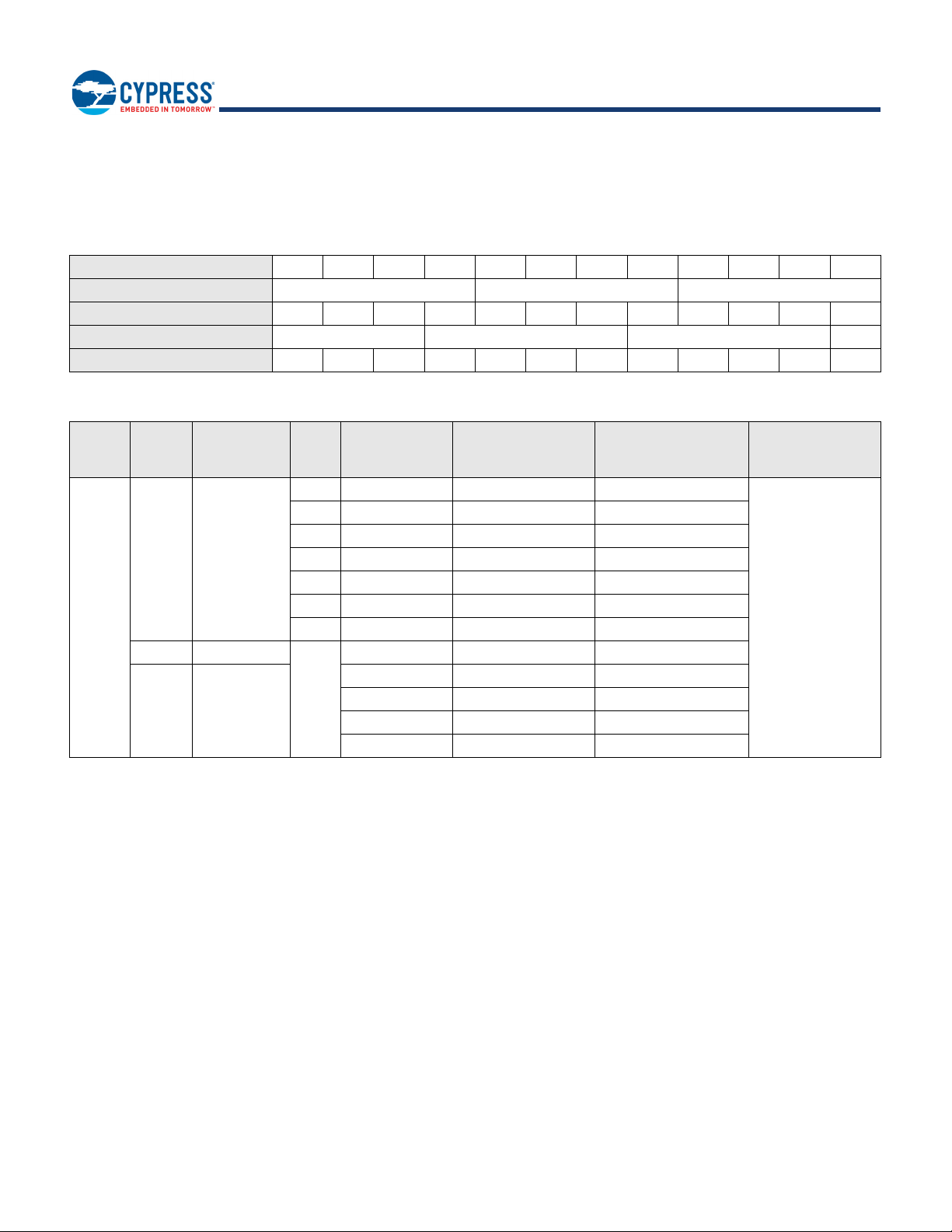
1.1 Valid Combinations
Valid Combination list configurations are planned to be supported in volume for this device. Consult your local sales office to confirm
availability of specific valid combinations and to check on newly released combinations.
S29VS-R Valid Combinations (1) (2)
Base Ordering
Part Number
Speed Option
Package Type, Material,
and Temperature Range
Packing
Type
Model
Numbers
S29VS256R
S29VS128R
S29XS256R
0S, AA, AB BHW (3) 0, 3 (1) 00, 01 6.2 mm x 7.7 mm, 44-ball
S29XS128R
Notes:
1. Type 0 is standard. Specify other options as required.
2. BGA package marking omits leading S29 and packing type designator from ordering part number.
3. Industrial Temperature Range is also available. For device specification differences, please refer to the Specification Supplement with Publication Number
S29VS_XS-R_SP.
Package Type
(2)
Document Number: 002-00833 Rev. *L Page 3 of 74
Page 4

S29VS256R
S29VS128R
S29XS256R
S29XS128R
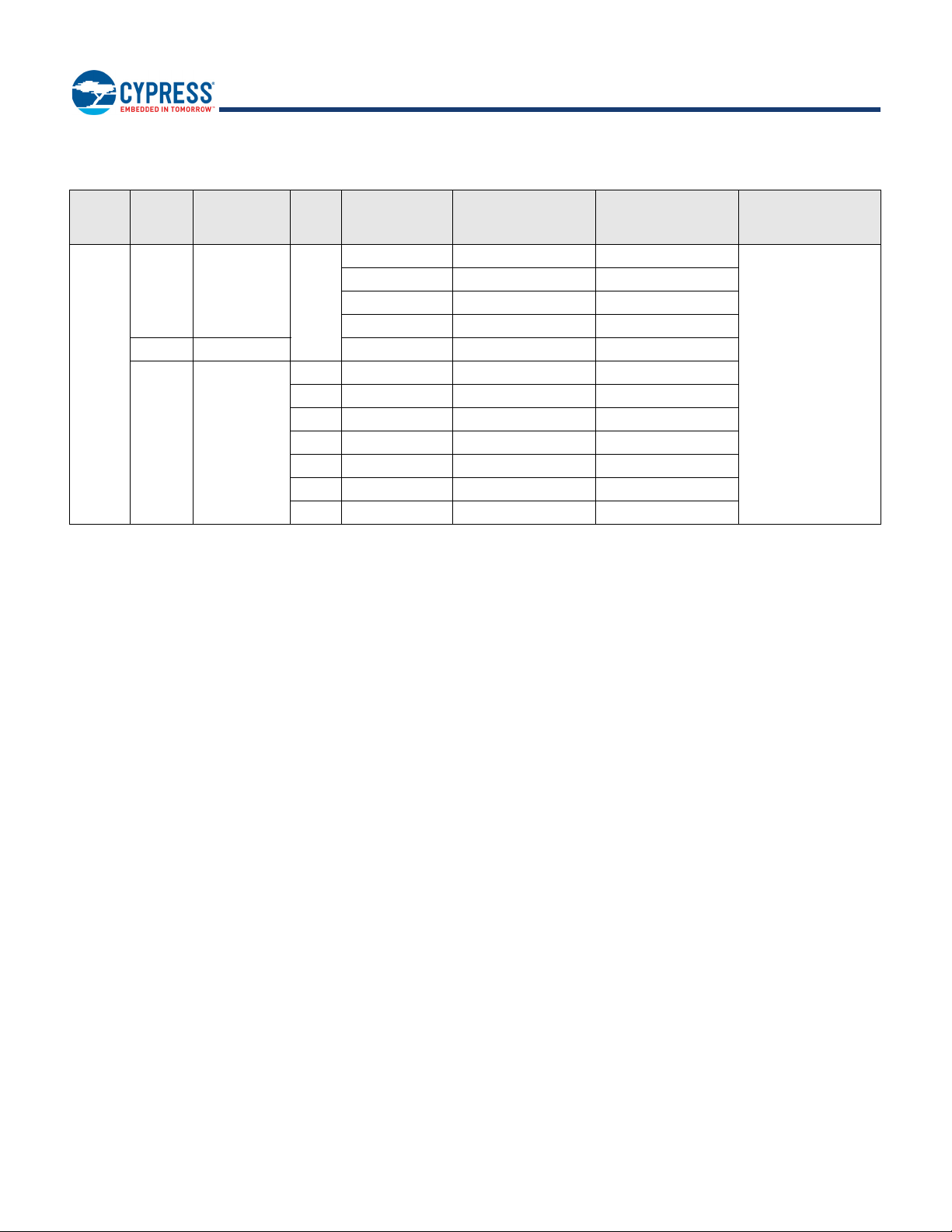
2. Input/Output Descriptions and Logic Symbol
Table 1 identifies the input and output package connections provided on the device.
Table 1. Input/Output Descriptions
Symbol Type Description
Amax – A16
A/DQ15 – A/DQ0 I/O Multiplexed Address/Data input/output
CE# Input Flash Chip Enable. Asynchronous relative to CLK.
OE# Input Output Enable. Asynchronous relative to CLK for the Burst mode.
WE# Input Write Enable
V
CC
V
CCQ
V
SS
V
SSQ
NC No Connect No Connected internally
RDY Output Ready. Indicates when valid burst data is ready to be read
CLK Input
AVD# Input
RESET# Input Hardware Reset. Low = device resets and returns to reading array data.
V
PP
RFU Reserved Reserved for future use
Supply Device Power Supply
Supply Input/Output Power Supply (must be ramped simultaneously with VCC)
I/O Ground
I/O Input/Output Ground
Input
Higher order address lines. Amax = A23 for VS256R, A22 for VS128R.
On the XS256R and XS128R, these inputs can be left unconnected in AADM mode.
The first rising edge of CLK in conjunction with AVD# low latches address input and activates
burst mode operation. After the initial word is output, subsequent rising edges of CLK increment
the internal address counter. CLK should remain low during asynchronous access
Address Valid input. Indicates to device that the valid address is present on the address inputs
(address bits A15 – A0 are multiplexed, address bits Amax – A16 are address only).
V
= for asynchronous mode, indicates valid address; for burst mode, cause staring address to
IL
be latched on rising edge of CLK.
VIH = device ignores address inputs
Accelerated input.
At V
, accelerates programming; automatically places device in unlock bypass mode.
HH
, disables all program and erase functions.
At V
IL
Should be at V
for all other conditions.
IH
Document Number: 002-00833 Rev. *L Page 4 of 74
Page 5

S29VS256R
S29VS128R
S29XS256R
S29XS128R
3. Block Diagram
V
CC
V
SS
V
SSQ
Figure 1. Simultaneous Operation Circuit
Bank Address
Y-Decoder
Amax–A0
X-Decoder
Bank Address
Y-Decoder
Bank 0
Bank 1
Latches and
Control Logic
Latches and
Control Logic
DQ15–DQ0
OE#
DQ15–DQ0
VPP
RESET#
WE#
CE#
AVD #
RDY
DQ15–DQ0
Amax–A0
Amax–A0
STATE
CONTROL
&
COMMAND
REGISTER
Amax–A0
Notes:
1. Amax = A23 for S29VS/XS256R, A22 for S29VS/XS128R.
2. Bank(n) = 8 (S29VS/XS256/128R).
Bank Address
Bank Address
Status
Control
Y-Decoder
Y-Decoder
X-Decoder
X-Decoder
Bank (n-1)
X-Decoder
Bank (n)
Latches and
Control Logic
Latches and
Control Logic
DQ15–DQ0
DQ15–DQ0
DQ15–DQ0
Document Number: 002-00833 Rev. *L Page 5 of 74
Page 6
S29VS256R
S29VS128R
S29XS256R
S29XS128R
4. Physical Dimensions/Connection Diagrams
32910547681 1312 1411
NC NC
B
D
E
F
G
H
A
C
RDY VPP A19VSSA21 VCCCLK WE# A22A17
VCCQ NC A18A20A16 A23AVD# RESET# VSSQCE#
VSS A/DQ2 A/DQ9A/DQ6A/DQ7 A/DQ12A/DQ13 A/DQ3 OE#A/DQ8
A/DQ15 A/DQ10 VCCQVSSQA/DQ14 A/DQ4A/DQ5 A/DQ11 A/DQ0A/DQ1
NC NC
This section shows the I/O designations and package specifications for the S29VS-R/S29XS-R.
4.1 Related Documents
The following document contains information relating to the S29VS-R/S29XS-R devices. Click on the title or go to www.cypress.com,
or request a copy from your sales office.
Considerations for X-ray Inspection of Surface-Mounted Flash Integrated Circuits
4.2 Special Handling Instructions for FBGA Package
Special handling is required for Flash Memory products in FBGA packages.
Flash memory devices in FBGA packages may be damaged if exposed to ultrasonic cleaning methods. The package and/or data
integrity may be compromised if the package body is exposed to temperatures above 150°C for prolonged periods of time.
4.2.1 44-Ball Very Thin Fine-Pitch Ball Grid Array, S29VS256R/S29XS256R/
S29VS128R/S29XS128R
Figure 2. 44-Ball Very Thin Fine-Pitch Ball Grid Array, Top View, Balls Facing Down
Notes:
1. Ball D7 is NC for S29VS128R.
2. Balls D7, C12, C4, D5, C10, D10, C11, D4 are NC for S29XS256R and S29XS128R
Document Number: 002-00833 Rev. *L Page 6 of 74
Page 7
S29VS256R
S29VS128R
S29XS256R
S29XS128R
4.2.2 VDJ044-44-Ball Very Thin Fine-Pitch Ball Grid Array, 6.2 mm x 7.7 mm
002-24745 **
Figure 3. VDJ044—44-Ball Very Thin Fine-Pitch Ball Grid Array
Document Number: 002-00833 Rev. *L Page 7 of 74
Page 8
S29VS256R
S29VS128R
S29XS256R
S29XS128R
5. Product Overview
The S29VS/XS-R family is 1.8-V only, simultaneous read/write, burst-mode, Flash devices. These devices have a 16 bit (word) wide
data bus. All read accesses provide 16 bits of data on each bus transfer cycle. All writes take 16 bits of data from each bus transfer
cycle.
Device Mbits Mbytes Mwords Banks Mbytes / Bank
S29VS128R/S29XS128R 128 16 8 8 2
S29VS256R/S29XS256R 256 32 16 8 4
The Flash memory array is divided into banks. A bank is the address range within which one program, or erase operation may be in
progress at the same time as one read operation is in progress in any other bank of the memory. This multiple bank structure
enables Simultaneous Read and Write (SRW) so that code may be executed or data read from one bank while a group of data is
programmed, or erased as a background task in one other bank.
Each bank is divided into sectors. A sector is the minimum address range of data which can be erased to an all Ones state. Most of
the sectors are 128 KBytes each. Depending on the option ordered, either the top-4 sectors or the bottom-4 sectors are 32 KBytes
each. These are called boot sectors because they are often used for holding boot code or parameters that need to be protected or
erased separately from other data in the Flash array.
Programming is done via a 64 Byte write buffer. It is possible to program from one to 32 words (64 bytes) in each programming
operation.
The S29VS/XS family is capable of continuous, synchronous (burst) read or linear read (8- or 16-word aligned group) with wrap
around. A wrapped burst begins at the initial location and continues to the end of an 8, or 16-word aligned group then
“wraps-around” to continue at the beginning of the 8, or 16-word aligned group. The burst completes with the last word before the
initial location. Word wrap around burst is generally used for processor cache line fill.
Document Number: 002-00833 Rev. *L Page 8 of 74
Page 9

S29VS256R
S29VS128R
S29XS256R
S29XS128R
6. Address Space Maps
There are five address spaces within each device:
A Non-Volatile Flash Memory Array used for storage of data that may be randomly accessed by asynchronous or burst read
operations.
A Read Only Memory Array used for factory programmed permanent device characteristics information. This area contains the
Device Identification (ID) and Common Flash Interface (CFI) information.
A One Time Programmable (OTP) Non-volatile Flash array used for factory programmed permanent data, and customer
programmable permanent data. This is called the Secure Silicon Region (SSR).
An OTP location used to permanently protect the SSR. This is call the SSR Lock.
A volatile register used to configure device behavior options. This is called the Configuration Register.
The main Flash Memory Array is the primary and default address space but, it may be partially overlaid by the other four address
spaces with one alternate address space available at any one time. The location where the alternate address space is overlaid is
defined by the address provided in the command that enables each overlay. The portion of the command address that is sufficient to
select a sector is used to select the sector that is overlaid by an alternate Address Space Overlay (ASO).
Any address range, within the overlaid sector, not defined by an overlay address map, is reserved for future use. All read accesses
outside of an address map within the selected sector, return non-valid data. The locations will display actively driven data but the
meaning of whatever ones or zeros appear are not defined.
There are three operation modes for each bank that determine what portions of the address space are readable at any given time:
Read Mode
Embedded Algorithm (EA) Mode
Address Space Overlay (ASO) Mode
Each bank of the device can be in any operation mode but, only one bank can be in EA or ASO mode at any one time.
In Read Mode, a Flash Memory Array bank may be directly read by asynchronous or burst accesses from the host system bus. The
Control Unit (CU) puts all banks in Read mode during Power-on, a Hardware Reset, after a Command Reset, or after a bank is
returned to Read mode from EA mode.
In EA mode the Flash memory array data in a bank is stable but undefined, and effectively unavailable for read access from the host
system. While in EA mode the bank is used by the CU in the execution of commands. Typical EA mode operations are programming
or erasing of data in the Flash array. All other banks are available for read access while the one bank is in EA mode. This ability to
read from one bank while another bank is used in the execution of a command is called Simultaneous Read and Write (SRW) and
allows for continued operation of the system via the reading of data or execution of code from other banks while one bank is
programming or erasing data as a relatively long time frame background task.
In ASO mode, one of the overlay address spaces are overlaid in a bank (entered). That bank is in ASO mode and no other bank may
be in EA or ASO mode. All EA activity must be completed before entering any ASO mode. A command for entering an EA or ASO
mode while another bank is in EA or ASO mode will be ignored.
While an ASO mode is active (entered) in a bank, a read for Flash array data to any other bank is allowed. ASO mode selects a
specific sector for the overlaid address space. Other sectors in the ASO bank still provide Flash array data and may be read during
ASO mode.
The ASOs are functionally tied to the lowest address bank. The commands used to overlay (enter) these areas must select a sector
address within the lowest address bank.
While SSR Lock, SSR, or Configuration Register is overlaid only the SSR Lock, SSR, or Configuration Register respectively may be
programmed in the overlaid sector. While any of these ASO areas are being programmed the ASO bank switches to EA mode. The
ID/CFI and factory portion of the SSR ASO is not customer programmable.
The address nomenclature used in this document is a shorthand form that shows addresses are formed from a concatenation of
high order bits, sufficient to select a Sector Address (SA), with low order bits to select a location within the sector. When in Read
mode and reading from the Flash Array the entire address is used to select a specific word for asynchronous read or the starting
word address of a burst read. When writing a command, the address bits between SA and the command specified least significant
bits must be Zero to allow for future extension of an overlay address map.
Document Number: 002-00833 Rev. *L Page 9 of 74
Page 10

S29VS256R
S29VS128R
S29XS256R
S29XS128R
6.1 Data Address and Quantity Nomenclature
A Bit is a single One or Zero data value. A Byte is a group of 8 bits aligned on an 8 bit boundary. A Word is a group of 16 bits aligned
on a 16 bit boundary.
Throughout this document quantities of data are generally expressed in terms of byte units. Example: most sectors have 128
Kilo Bytes of data and is written as 128 KBytes or 128 KB. Addresses are also expressed in byte units. A 128 KByte sector has
an address range from 00000h to 1FFFFh Byte locations. Byte units are used because most host systems and software for these
systems use byte resolution addresses. Software & hardware developers most often calculate code and data sizes in terms of bytes,
so this is more familiar terminology than describing data sizes in bits or words. In general, data units will not be abbreviated if
possible so that full unit names of Byte, Word, or bit are used. However, there may be cases where capital B is used for byte units
and lower case b is used for bit units, in situations where space is limited such as in table column headers.
In some cases data quantities will also be expressed in word or bit units in addition to the quantity shown in bytes. This may be done
as an aid to readers familiar with prior device generation documentation which often provided only word or bit unit values. Word units
may also be used to emphasize that, in the memory devices described in this documentation, data is always exchanged with the
host system in word units. Each bus cycle transfer of read or write data on the host system bus is a transfer 16 bits of data. A read
bus cycle is always a16 bit wide transfer of data to the host system whether the host system chooses to look at all the bits or not. A
write bus cycle is always a transfer of 16 bits to the memory device and the device will store all 16 bits to a register. In the case of a
program operation all 16 bits of each word to be programmed will be stored in the Flash array.
Because data is always transferred in word units, the memory devices being discussed use only the address signals from the
system necessary to select words. The host system byte address uses system address a0 to select bytes and a1 to select words.
Flash memories with word wide data paths have traditionally started their address signal numbering with A0 being the selector for
words because a byte select input is not needed. So, system address a-maximum to a1 are connected to Flash A-maximum to A0
(the documentation convention here is to use lower case for system address signal numbering and upper case for Flash address
signals). In prior generation Flash documentation, address values used in commands to the flash were documented from the
viewpoint of the Flash device - the bit pattern appearing on Flash address inputs A10 to A0. However, most software is written
addresses expressed in bytes. This means the address patterns shown in Flash command tables have traditionally been shifted by
one bit to express them as byte address values in Flash control programs. Example: a prior generation Flash data sheet would show
a command write of data value xxA0h to address 555h; this is an address pattern of 10101010101b on Flash address inputs A10 to
A0; but software would define this as a byte address value of AAAh since the least significant address bit is not used by the Flash);
which is 101010101010b on system address bus a11 to a0. Because system a11 to a1 is connected to Flash A10 to A0 the Flash
word address of 555h and the system byte address of AAAh provides the same bit pattern on the same address inputs. Because all
address values are being documented as system byte addresses, that are more familiar to software writers, the command tables
have addresses that are shifted from those shown in prior generation devices.
with
Document Number: 002-00833 Rev. *L Page 10 of 74
Page 11
S29VS256R
S29VS128R
S29XS256R
S29XS128R
6.2 Flash Memory Array
The Non-Volatile Flash Memory Array is organized as shown in the following tables. Devices are factory configured to have either all
uniform size sectors or four smaller sectors at either the top of the device.
Table 2. System Versus Flash View of Address
System Address Signals a11 a10 a9 a8 a7 a6 a5 a4 a3 a2 a1 a0
System Byte Address Hex AAA
Binary Pattern 101010101010
Flash Word Address Hex 55 5
Flash Address Signals A10A9A8A7A6A5A4A3A2A1A0
Table 3. S29VS/XS256R Sector and Memory Address Map (Top Boot)
Bank
Size
(Mbit)
32
Sector
Count
224 128
31 128
Sector Size
(KByte)
432
Bank
0 SA000-SA031 000000h–1FFFFFh 000000h–3FFFFFh
1 SA032–SA063
2 SA064–SA095
3 SA096–SA127
4 SA128–SA159
5 SA160–SA191
6 SA192–SA223
7
Sector
Range
SA224–SA254 E00000h–FEFFFFh 1C00000h–1FDFFFFh
SA255 FF0000h–FF3FFFh 1FE0000h–1FE7FFFh
SA256 FF4000h-FF7FFFh 1FE8000h-1FEFFFFh
SA257 FF8000h–FFBFFFh 1FF0000h–1FF7FFFh
SA258 FFC000h–FFFFFFh 1FF8000h–1FFFFFFh
Address
Range (word)
…
…
…
…
…
…
Address
Range (byte)
…
…
…
…
…
…
Notes
Sector Starting
Address –
Sector Ending
Address
Note:
All tables have been condensed to show sector-related information for an entire device on a single page. Sectors and their address ranges that are not explicitly listed
(such as SA008–SA009) have sector starting and ending addresses that form the same pattern as all other sectors of that size. For example, all 128 KB sectors have the
byte address pattern x000000h–x1FFFFh.
Document Number: 002-00833 Rev. *L Page 11 of 74
Page 12

S29VS256R
S29VS128R
S29XS256R
S29XS128R
Table 4. S29VS/XS256R Sector and Memory Address Map (Bottom Boot)
Bank
Size
(Mbit)
Note:
All tables have been condensed to show sector-related information for an entire device on a single page. Sectors and their address ranges that are not explicitly listed
(such as SA008–SA009) have sector starting and ending addresses that form the same pattern as all other sectors of that size. For example, all 128 KB sectors have the
byte address pattern x000000h–x1FFFFh.
32
Sector
Count
31 128 SA004–SA034 010000h–1FFFFFh 020000h–3FFFFFh
224 128
Sector Size
(Kbyte)
432
Bank
Sector
Range
SA000 000000h–003FFFh 000000h–007FFFh
SA001 004000h–007FFFh 008000h–00FFFFh
0
1 SA035–SA066
2 SA067–SA098
3 SA099–SA130
4 SA131–SA162
5 SA163–SA194
6 SA195–SA226
7 SA227–SA258 E00000h–FFFFFFh 1C00000h–1FFFFFFh
SA002 008000h–00BFFFh 010000h–017FFFh
SA003 00C000h–00FFFFh 018000h–01FFFFh
Address
Range (word)
…
…
…
…
…
…
Address
Range (byte)
…
…
…
…
…
…
Notes
Sector Starting
Address –
Sector Ending
Address
Table 5. S29VS/XS128R Sector and Memory Address Map (Top Boot)
Bank
Size
(Mbit)
16
Note:
All tables have been condensed to show sector-related information for an entire device on a single page. Sectors and their address ranges that are not explicitly listed
(such as SA008–SA009) have sector starting and ending addresses that form the same pattern as all other sectors of that size. For example, all 128 KB sectors have the
byte address pattern x000000h–x1FFFFh.
Sector
Count
112 128
15 128
Sector Size
(KByte)
432
Bank
0 SA000-SA015 000000h–0FFFFFh 000000h–1FFFFFh
1 SA016–SA031
2 SA032–SA047
3 SA048–SA063
4 SA064–SA079
5 SA080–SA095
6 SA096–SA111
7
Sector
Range
SA112–SA126 700000h–7EFFFFh E00000h–FDFFFFh
SA127 7F0000h–7F3FFFh FE0000h–FE7FFFh
SA128 7F4000h-7F7FFFh FE8000h-FEFFFFh
SA129 7F8000h–7FBFFFh FF0000h–FF7FFFh
SA130 7FC000h–7FFFFFh FF8000h–FFFFFFh
Address
Range (word)
…
…
…
…
…
…
Address
Range (byte)
…
…
…
…
…
…
Notes
Sector Starting
Address –
Sector Ending
Address
Document Number: 002-00833 Rev. *L Page 12 of 74
Page 13
S29VS256R
S29VS128R
S29XS256R
S29XS128R
Table 6. S29VS/XS128R Sector and Memory Address Map (Bottom Boot)
Bank
Size
(Mbit)
16
Note:
All tables have been condensed to show sector-related information for an entire device on a single page. Sectors and their address ranges that are not explicitly listed
(such as SA008–SA009) have sector starting and ending addresses that form the same pattern as all other sectors of that size. For example, all 128 KB sectors have the
byte address pattern x000000h–x1FFFFh.
Sector
Count
15 128 SA004–SA018 010000h–0FFFFFh 020000h–1FFFFFh
112 128
Sector Size
(Kbyte)
432
Bank
Sector
Range
SA000 000000h–003FFFh 000000h–007FFFh
SA001 004000h–007FFFh 008000h–00FFFFh
0
1 SA019–SA034
2 SA035–SA050
3 SA051–SA066
4 SA067–SA082
5 SA083–SA098
6 SA099–SA114
7 SA115–SA130 700000h–7FFFFFh E00000h–FFFFFFh
SA002 008000h–00BFFFh 010000h–017FFFh
SA003 00C000h–00FFFFh 018000h–01FFFFh
Address
Range (word)
…
…
…
…
…
…
Address
Range (byte)
…
…
…
…
…
…
Notes
Sector Starting
Address –
Sector Ending
Address
6.3 Address/Data Interface
There are two options for connection to the address and data buses.
Address and Data Multiplexed (ADM) mode. On the S29VS-R devices, the upper address is supplied on separate signal inputs
and the lower 16-bits of address are multiplexed with 16-bit data on the A/DQ15 to A/DQ0 I/Os.
Address-high, Address-low, and Data Multiplexed (AADM) mode. On the S29XS-R devices, the upper and lower address are
multiplexed with 16-bit data on the A/DQ15 to A/D0 signal I/Os.
The two options allow use with the traditional address/data multiplexed NOR interface (S29NS family), or an address
multiplexed/data multiplexed interface with the lowest signal count.
6.3.1 ADM Interface (S29VS256R and S29VS128R)
A number of processors use ADM interface as a way to reduce pin count. The system permanently connects the upper address bits
(A[MAX:16] to the device. When AVD# is LOW it connects A[15:0] to DQ[15:0]. The address is latched on the rising edge of AVD#.
When AVD# is HIGH, the system connects the data bus to DQ[15:0]. This results in 16-pin savings from the traditional Address and
Data in Parallel (ADP) interface.
6.3.2 AADM Interface (S29XS256R and S29XS128R)
Signal input and output (I/O) connections on a high complexity component such as an Application Specific Integrated Circuit (ASIC)
are a limited resource. Reducing signal count on any interface of the ASIC allows for either more features or lower package cost.
The memory interface described in this section is intended to reduce the I/O signal count associated with the Flash memory interface
with an ASIC.
The interface is called Address-High, Address-Low, and Data Multiplexed (AADM) because all address and data information is time
multiplexed on a single 16-bit wide bus. This interface is electrically compatible with existing ADM 16-bit wide random access static
memory interfaces but uses fewer address signals. In that sense AADM is a signal count subset of existing static memory interfaces.
This interface can be implemented in existing memory controller designs, as an additional mode, with minimal changes. No new
I/O technology is needed and existing memory interfaces can continue to be supported while the electronics industry adopts this
new interface. ASIC designers can reuse the existing memory address signals above A15 for other functions when an AADM
memory is in use.
Document Number: 002-00833 Rev. *L Page 13 of 74
Page 14

S29VS256R
S29VS128R
S29XS256R
S29XS128R
By breaking up the memory address in to two time slots the address is naturally extended to be a 32-bit word address. But, using
two bus cycles to transfer the address increases initial access latency by increasing the time address is using the bus. However,
many memory accesses are to locations in memory nearby the previous access. Very often it is not necessary to provide both cycles
of address. This interface stores the high half of address in the memory so that if the high half of address does not change from the
previous access, only the low half of address needs to be sent on the bus. If a new upper address is not captured at the beginning of
an access the last captured value of the upper address is used. This allows accesses within the same 128-KByte address range to
provide only the lower address as part of each access.
In AADM mode two signal rising edges are needed to capture the upper and lower address portions in asynchronous mode or two
signal combinations over two clocks is needed in synchronous mode. In asynchronous mode the upper address is captured by an
AVD# rising edge when OE# is Low; the lower address is captured on the rising edge of AVD# with OE# High. In synchronous mode
the upper address is captured at the rising clock edge when AVD# and OE# are Low; the lower address is captured at the rising
edge of clock when AVD# is Low and OE# is High.
CE# going High at any time during the access or OE# returning High after RDY is first asserted High during an access, terminates
the read access and causes the address/data bus direction to switch back to input mode. The address/data bus direction switches
from input to output mode only after an Address-Low capture when AVD# is Low and OE# is High. This prevents the assertion of
OE# during Address-High capture from causing a bus conflict between the host address and memory data signals. Note, in burst
mode, this implies at least one cycle of CE# or OE# High before an Address-high for a new access may be placed on the bus so that
there is time for the memory to recognize the end of the previous access, stop driving data outputs, and ignore OE# so that assertion
of OE# with the new Address-high does not create a bus conflict with a new address being driven on the bus. At high bus
frequencies more than one cycle may be need in order to allow time for data outputs to stop driving and new address to be driven
(bus turn around time).
During a write access, the address/data bus direction is always in the input mode.
The upper address is set to Zero or all Ones, for bottom or top boot respectively, during a Hardware Reset, operate in ADM mode
during the early phase of boot code execution where only a single address cycle would be issued with the lower 16 bit of the address
reaching the memory in AADM mode. The default high order address bits will direct the early boot accesses to the 128 Kbytes at the
boot end of the device. Note that in AADM interface mode this effectively requires that one of the boot sectors is selected for any
address overlay mode because in the initial phase of AADM mode operation the host memory controller may only issue the low
order address thus limiting the early boot time address space to the 128 Kbytes at the boot end of the device.
6.3.3 Default Access Mode
Upon power-up or hardware reset, the device defaults to the Asynchronous Access mode.
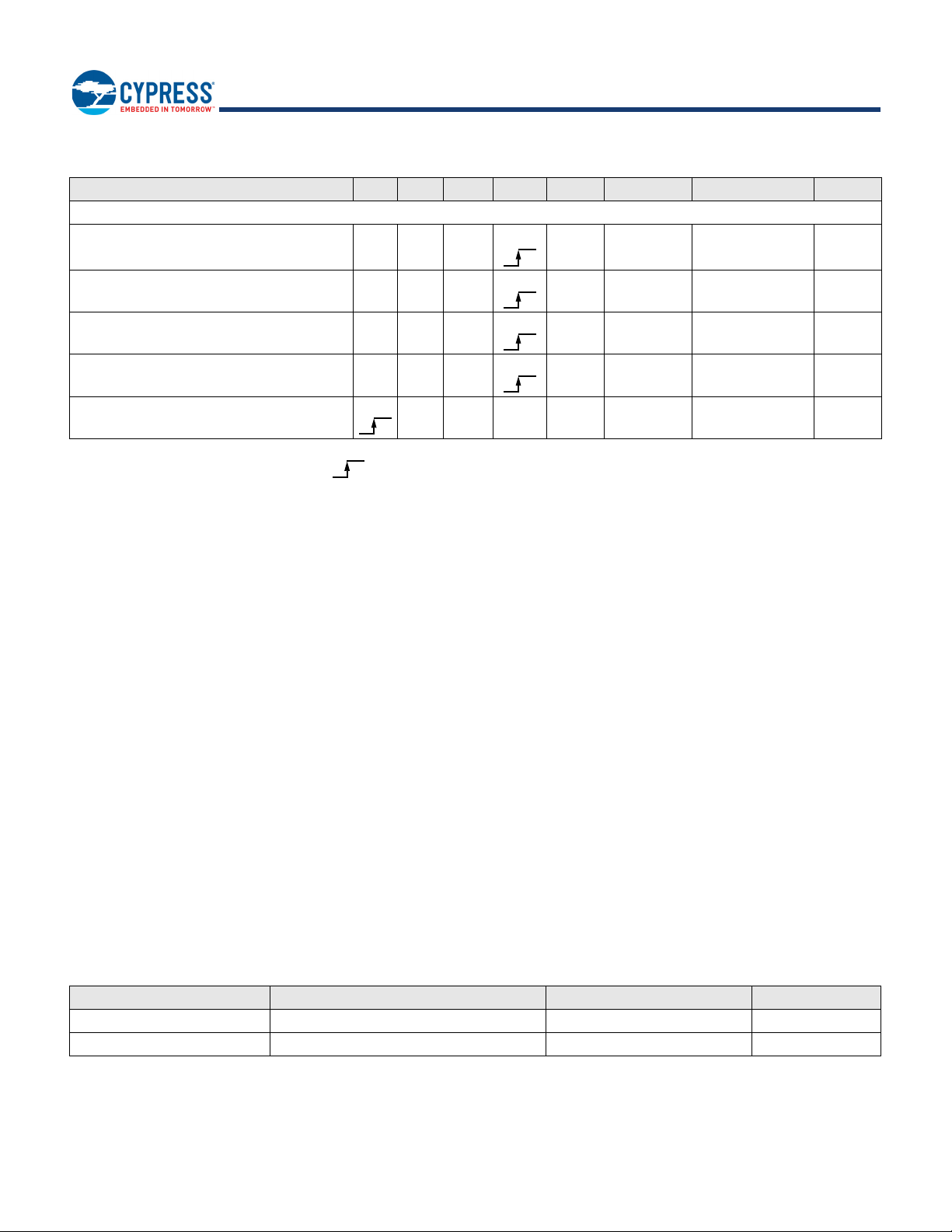
6.4 Bus Operations
Table 7 describes the required state of each input signal for each bus operation.
Table 7. Device Bus Operations
Operation CE# OE# WE# CLK AVD# A28-A16 A/DQ 15-A/DQ0 RESET#
Standby & Reset
Standby (CE# deselect) H X X X X X High-Z H
Hardware Reset X X X X X X High-Z L
Asynchronous Mode Operations
Asynchronous Address Latch
(S29VS256R and S29VS128R)
Asynchronous Upper Address Latch
(S29XS256R and S29XS128R Only)
Asynchronous Lower Address Latch
(S29XS256R and S29XS128R Only)
Asynchronous Read L L H X H X Data Output Valid H
Asynchronous Write Latched Data L H X H X Data Input Valid H
L H X X Addr In Addr In H
L L H X X Addr In H
L H X X X Addr In H
Document Number: 002-00833 Rev. *L Page 14 of 74
Page 15
S29VS256R
S29VS128R
S29XS256R
S29XS128R
Table 7. Device Bus Operations (Continued)
Operation CE# OE# WE# CLK AVD# A28-A16 A/DQ 15-A/DQ0 RESET#
Latch Starting Burst Address by CLK
- ADM mode
Synchronous Mode Operations
L H H L Addr In Addr In H
Latch Upper Starting Burst Address by CLK
(S29XS256R and S29XS128R Only)
Latch Lower Starting Burst Address by CLK
(S29XS256R and S29XS128R Only)
Burst Read and advance to next address (1) L L H H X Data Output Valid H
Terminate current Burst cycle X X X X X High-Z H
Legend:
L = Logic 0, H = Logic 1, X = can be either V
Note:
1. Data is delivered by a read operation only after the burst initial wait state count has been satisfied.
or VIH. = rising edge.
IL
L L H L X Addr In H
L H H L X Addr In H
6.5 Device ID and CFI (ID-CFI)
There are two traditional methods for systems to identify the type of Flash memory installed in the system. One has been
traditionally been called Autoselect and is now referred to as Device Identification (ID). A command is used to enable an address
space overlay where up to 16 word locations can be read to get JEDEC manufacturer identification (ID), device ID, and some
configuration and protection status information from the Flash memory. The system can use the manufacturer and device IDs to
select the appropriate driver software to use with the Flash device. The other method is called Common Flash Interface (CFI). It also
uses a command to enable an address space overlay where an extendable table of standard information about how the Flash
memory is organized and behaves can be read. With this method the driver software does not have to be written with the specifics of
each possible memory device in mind. Instead the driver software is written in a more general way to handle many different devices
but adjusts the driver behavior based on the information in the CFI table stored in the Flash memory. Traditionally these two address
spaces have used separate commands and were separate overlays. However, the mapping of these two address spaces are
non-overlapping and so can be combined in to a single address space and appear together in a single overlay. Either of the
traditional commands used to access (enter) the Autoselect (ID) or CFI overlay will cause the now combined ID-CFI address map to
appear.
A write at any sector address, in bank zero, having the least significant byte address value of AAh, with xx98h or xx90h data,
switches the addressed sector to an overlay of the ID-CFI address map. These are called ID-CFI Enter commands and are only valid
when written to the specified bank when it is in read mode. The ID-CFI address map appears within, and replaces Flash Array data
of, the selected sector address range. The ID-CFI enter commands use the same address and data values used on previous
generation memories to access the JEDEC Manufacturer ID (Autoselect) and Common Flash Interface (CFI) information,
respectively. While the ID-CFI address space is overlaid, any write with xxF0h data to the device will remove the overlay and return
the selected sector to showing Flash memory array data. Thus, the ID-CFI address space and commands are backward compatible
with standard memory discovery algorithms.
Within the ID-CFI address map there are two subsections:
Table 8. ID-CFI Address Map Overview
Byte Address Description Size Allocated (Bytes) Read/Write
(SA) + 00000h to 0001Fh JEDEC ID (traditional Autoselect values) 32 Read Only
(SA) + 00020h to CEh h CFI data structure 174 Read Only
For the complete address map, see Tables in Section 11.2, Device ID and Common Flash Memory Interface Address Map
on page 59.
Document Number: 002-00833 Rev. *L Page 15 of 74
Page 16
S29VS256R
S29VS128R
S29XS256R
S29XS128R
6.5.1 JEDEC Device ID
The Joint Electron Device Engineering Council (JEDEC) standard JEP106T defines a method for reading the manufacturer ID and
device ID of a compliant memory. This information is primarily intended for programming equipment to automatically match a device
with the corresponding programming algorithm.
The JEDEC ID information is structured to work with any memory data bus width e.g. x8, x16, x32. The code values are always byte
wide but are located at bus width address boundaries such that incrementing the device address inputs will read successive byte,
word, or double word locations with the codes always located in the least significant byte location of the data bus. Because the data
bus is word wide each code byte is located in the lower half of each word location and the high order byte is always zero.
6.5.2 Common Flash Memory Interface
The Common Flash Interface (CFI) specification defines a standardized data structure that may be read from a flash memory
device, which allows vendor-specified software algorithms to be used for entire families of devices. The data structure contains
information for system configuration such as various electrical and timing parameters, and special functions supported by the
device. Software support can then be device-independent, JEDEC ID-independent, and forward-and-backward-compatible for the
specified flash device families.
The system can read CFI information at the addresses within the selected sector as shown in Section 11.2, Device ID and Common
Flash Memory Interface Address Map on page 59.
Like the JEDEC Device ID information, CFI information is structured to work with any memory data bus width e.g. x8, x16, x32. The
code values are always byte wide but are located at data bus width address boundaries such that incrementing the device address
reads successive byte, word, or double word locations with the codes always located in the least significant byte location of the data
bus. Because the data bus is word wide each code byte is located in the lower half of each word location and the high order byte is
always zero.
For further information, please refer to the Cypress CFI Version 1.4 (or later) Specification and the Cypress CFI Publication 100 (see
also JEDEC publications JEP137-A and JESD68.01). Please contact JEDEC (http://www.jedec.org) for their standards and the
Cypress CFI Publications may be found at the Cypress Web site
(http://www.cypress.com/appnotes/CFI_v1.4_VendorSpec_Ext_A1.pdf at the time of this document’s publication).
6.5.3 Secured Silicon Region
The Secured Silicon region provides an extra Flash memory area that can be programmed once and permanently protected from
further changes. The Secured Silicon Region is 512 bytes in length. It consists of 256 bytes for factory data and 256 bytes for
customer-secured data.
The Secured Silicon Region (SSR) is overlaid in the sector address specified by the SSR enter command.
Table 9. Secured Silicon Region
Byte Address Range Secure Silicon Region Size
(SA) + 0000h to 00FFh Factory 256 Bytes
(SA) + 0100h to 01FFh Customer 256 Bytes
6.5.4 Configuration Register
The Configuration Register Enter command is only valid when written to a bank that is in Read mode. The configuration register
mode address map appears within, and replaces Flash Array data of, the selected sector address range. The meaning of the
configuration register bits is defined in the configuration register operation description. In configuration register mode, a write of
00F0h to any address will return the sector to Read mode.
Document Number: 002-00833 Rev. *L Page 16 of 74
Page 17

S29VS256R
S29VS128R
S29XS256R
S29XS128R
7. Device Operations
This section describes the read and write bus operations, program, erase, simultaneous read/write, handshaking, and reset features
of the Flash devices.
The address space of the Flash Memory Array is divided into banks. There are three operation modes for each bank:
Read Mode
Embedded Algorithm (EA) Mode
Address Space Overlay (ASO) Mode
Each bank of the device can be in any operation mode but, only one bank can be in EA or ASO mode at any one time.
In Read Mode a Flash Memory Array bank may be read by simply selecting the memory, supplying the address, and taking read
data when it is ready. This is done by asynchronous or burst accesses from the host system bus. The CU puts all banks in Read
mode during Power-on, a Hardware Reset, after a Command Reset, or after a bank is returned to Read mode from EA mode.
During a burst read access valid read data is indicated by the RDY signal being High. When RDY is Low burst read data is not valid
and wait states must be added. The use of the RDY signal to indicate when valid data is transferred on the system data bus is called
handshaking or flow control.
EA and ASO modes are initiated by writing specific address and data patterns into command registers (see Table 43 on page 57).
The command registers do not occupy any memory locations; they are loaded by write bus cycles with the address and data
information needed to execute a command. The contents of the registers serve as input to the Control Unit (CU) and the CU dictates
the function of the device. Writing incorrect address and data values or writing them in an improper sequence may place the device
in an unknown state, in which case the system must write the reset command to return all banks to Read mode.
The Flash memory array data in a bank that is in EA mode, is stable but undefined, and effectively unavailable for read access from
the host system. While in EA mode the bank is used by the CU in the execution of commands. Typical command operations are
programming or erasing of data in the Flash array. All other banks are available for read access while the one bank is in EA mode.
This ability to read from one bank while another bank is used in the execution of a command is called Simultaneous Read and Write
(SRW) and allows for continued operation of the system via the reading of data or code from other banks while one bank is
programming or erasing data as a relatively long time frame background task. Only a status register read command can be used in
a bank in EA mode to retrieve the EA status.
While any one of the overlay address spaces are overlaid in a bank (entered) that bank is in ASO mode and no other bank may be
in EA or ASO mode. All EA activity must be completed or suspended before entering any ASO mode. A command for entering an EA
or ASO mode while another bank is in EA or ASO mode will be ignored.
While an ASO mode is active (entered) in a bank, a read for Flash array data to any other bank is allowed. ASO mode selects a
specific sector for the overlaid address space. Other sectors in the ASO bank still provide Flash array data and may be read during
ASO mode.
While SSR Lock, SSR, or Configuration Register is overlaid only the SSR Lock, SSR, or Configuration Register respectively may be
programmed in the overlaid sector. While any of these ASO areas are being programmed the ASO bank switches to EA mode. The
ID/CFI and factory portion of the SSR ASO is not customer programmable. An attempt to program in these areas will fail.
7.1 Asynchronous Read
The device defaults to reading array data asynchronously after device power-up or hardware reset. The device is in the
Asynchronous mode when Bit 15 of the Configuration register is set to '1'. To read data from the memory array, the system must first
assert CE# and AVD# to V
Address access time (t
delay from stable CE# to valid data at the outputs. See 10.9.2, AC Characteristics–Asynchronous Read on page 50. Any input on
CLK is ignored while in Asynchronous mode.
with WE# at VIH and a valid address.
IL
) is equal to the delay from stable addresses to valid output data. The chip enable access time (tCE) is the
ACC
Document Number: 002-00833 Rev. *L Page 17 of 74
Page 18

S29VS256R
S29VS128R
S29XS256R
S29XS128R
7.1.1 S29VS-R ADM Access
With CE# at VIL, WE# at VIH, and OE# at VIH, the system presents the address to the device and drives AVD# to VIL. AVD# is kept
at V
IL
for at least t
ns. The address is latched on the rising edge of AVD#.
AVD P
7.1.2 S29XS-R AADM Access
With CE# at VIL, WE# at VIH, and OE# at VIL, the system presents the upper address bits to DQ and drives AVD# to VIL. The upper
address bits are latched when AVD# transitions to VIH. The system then drives AVD# to VIL again, with OE# at VIH and the lower
address bits on the DQ signals. The lower address bits are latched on the next rising edge of AVD#.
7.2 Synchronous (Burst) Read Mode and Configuration Register
The device is capable of continuous sequential burst operation and linear burst operation of a preset length.
In order to use Synchronous (Burst) Read Mode the configuration register bit 15 must be set to 0.
Prior to entering burst mode, the system should determine how many wait states are needed for the initial word of each burst access
(see table below), what mode of burst operation is desired, how the RDY signal transitions with valid data, and output drive strength.
The system would then write the configuration register command sequence. See Configuration Register on page 23 for further
details.
When the appropriate number of Wait States have occurred, data is output after the rising edge of the CLK. Subsequent words are
output t
indicates the initial latency and any subsequent waits.
7.2.1 S29VS-R ADM Access
To burst read data from the memory array in ADM mode, the system must assert CE# to VIL, and provide a valid address while
driving AVD# to VIL for one cycle. OE# must remain at VIH during the one cycle that AVD# is at VIL. The data appears on A/DQ15
-A/DQ0 when CE# remains at V
burst sequence is read on each clock cycle that OE# and CE# remain at VIL.
OE# does not terminate a burst access if it rises to VIH during a burst access. The outputs will go to high impedance but the burst
access will continue until terminated by CE# going to VIH, or AVD# returns to VIL with a new address to initiate a another burst
access.
after the rising edge of each successive clock cycle, which automatically increments the internal address counter. RDY
BACC
, after OE# is driven to VIL and the synchronous access times are satisfied. The next data in the
IL
7.2.2 S29XS-R AADM Access
To burst read data from the memory array in AADM mode, the system must assert CE# to VIL, OE# must be driven to VIL with AVD#
for one cycle while the upper address is valid. The rising edge of CLK when OE# and AVD# are at VIL captures the upper 16 bits of
address. The rising edge of CLK when OE# is at V
A/DQ15 -A/DQ0 when CE# remains at VIL, after OE# is driven to VIL and the synchronous access times are satisfied. The next data
in the burst sequence is read on each clock cycle that OE# and CE# remain at V
Once OE# returns to VIH during a burst read the OE# no longer enables the outputs until after AVD# is at VIL with OE# at VIH - which
signals that address-low has been captured for the next burst access. This is so that OE# at VIL may be used in conjunction with
AVD# at V
with Address-high.
The device has a fixed internal address boundary that occurs every 256 Bytes (128 words). A boundary crossing latency of one or
two additional wait states may be required. The device also reads data in 16 byte (8 word) aligned and length groups. When the
initial address is not aligned at the beginning of a 16 byte boundary, additional wait states may be needed when crossing the first 16
byte boundary. The number of additional wait states depends on the clock frequency and starting address location.
to indicate address-high on the A/DQ signals without enabling the A/DQ outputs, thus avoiding data output contention
IL
and AVD# is at VIL latches the lower 16 bits of address. The data appears on
IH
.
IL
Document Number: 002-00833 Rev. *L Page 18 of 74
Page 19
S29VS256R
S29VS128R
S29XS256R
S29XS128R
Table 10 through Table 18 provide the latency for initial and boundary crossing wait state operation (note that ws = wait state).
Table 10. Initial Wait State vs. Frequency
Wait State Frequency (Maximum MHz)
327
440
554
666
780
895
9 104
10 120
Note:
The default initial wait state delay after power on or reset is 13 wait states.
Table 11. Address Latency for 10 -13 Wait States
Word Initial Wait Subsequent Clock Cycles After Initial Wait States
0
1 D1D2D3D4D5D6D71 ws+2 wsD8
2 D2D3D4D5D6D71 ws1 ws+2 wsD8
3 D3D4D5D6D71 ws1 ws1 ws+2 wsD8
4 D4 D5 D6 D7 1 ws 1 ws 1 ws 1 ws +2 ws D8
5 D5 D6 D7 1 ws 1 ws 1 ws 1 ws 1 ws +2 ws D8
6 D6 D7 1 ws 1 ws 1 ws 1 ws 1 ws 1 ws +2 ws D8
7 D7 1 ws 1 ws 1 ws 1 ws 1 ws 1 ws 1 ws +2 ws D8
10 -13 wait states
D0 D1 D2 D3 D4 D5 D6 D7 +2 ws (1) D8
Note:
1. This column applies to the 256 Byte boundary only.
Table 12. Address Latency for 9 Wait States
Word Initial Wait Subsequent Clock Cycles After Initial Wait States
0
1 D1D2D3D4D5D6D71 ws+1 wsD8
2 D2D3D4D5D6D71 ws1 ws+1 wsD8
3 D3D4D5D6D71 ws1 ws1 ws+1 wsD8
4 D4 D5 D6 D7 1 ws 1 ws 1 ws 1 ws +1 ws D8
5 D5 D6 D7 1 ws 1 ws 1 ws 1 ws 1 ws +1 ws D8
6 D6 D7 1 ws 1 ws 1 ws 1 ws 1 ws 1 ws +1 ws D8
7 D7 1 ws 1 ws 1 ws 1 ws 1 ws 1 ws 1 ws +1 ws D8
Note:
1. This column applies to the 256 Byte boundary only.
9 wait states
D0 D1 D2 D3 D4 D5 D6 D7 +1 ws (1) D8
Document Number: 002-00833 Rev. *L Page 19 of 74
Page 20
S29VS256R
S29VS128R
S29XS256R
S29XS128R
Table 13. Address Latency for 8 Wait States
Word Initial Wait Subsequent Clock Cycles After Initial Wait States
0
1 D1D2D3D4D5D6D71 wsD8
2 D2D3D4D5D6D71 ws1 wsD8
3 D3D4D5D6D71 ws1 ws1 wsD8
4 D4 D5 D6 D7 1 ws 1 ws 1 ws 1 ws D8
5 D5D6 D7 1 ws1 ws1 ws1 ws1 wsD8
6 D6 D7 1 ws 1 ws 1 ws 1 ws 1 ws 1 ws D8
7 D71 ws1 ws1 ws1 ws1 ws1 ws1 wsD8
Table 14. Address Latency for 7 Wait States
Word Initial Wait Subsequent Clock Cycles After Initial Wait States
0
1 D1D2D3D4D5D6D7D8D9
2 D2D3D4D5D6D71 wsD8D9
3 D3D4D5D6D71 ws1 wsD8D9
4 D4D5D6D71 ws1 ws1 wsD8D9
5 D5D6 D7 1 ws1 ws1 ws1 wsD8D9
6 D6D7 1 ws1 ws1 ws1 ws1 wsD8D9
7 D71 ws1 ws1 ws1 ws1 ws1 wsD8D9
8 wait states
7 wait states
D0 D1 D2 D3 D4 D5 D6 D7 D8
D0 D1 D2 D3 D4 D5 D6 D7 D8
Table 15. Address Latency for 6 Wait States
Word Initial Wait Subsequent Clock Cycles After Initial Wait States
0
1 D1D2D3D4D5D6D7D8D9
2 D2D3D4D5D6D7D8D9D10
3 D3D4D5D6D71 wsD8D9D10
4 D4 D5 D6 D7 1 ws 1 ws D8 D9 D10
5 D5 D6 D7 1 ws 1 ws 1 ws D8 D9 D10
6 D6D7 1 ws1 ws1 ws1 wsD8D9D10
7 D71 ws1 ws1 ws1 ws1 wsD8D9D10
6 wait states
D0 D1 D2 D3 D4 D5 D6 D7 D8
Document Number: 002-00833 Rev. *L Page 20 of 74
Page 21
S29VS256R
S29VS128R
S29XS256R
S29XS128R
Table 16. Address Latency for 5 Wait States
Word Initial Wait Subsequent Clock Cycles After Initial Wait States
0
1 D1D2D3D4D5D6D7D8D9
2 D2D3D4D5D6D7D8D9D10
3 D3D4D5D6D7D8D9D10D11
4D4D5D6D71 wsD8D9D10D11
5 D5 D6 D7 1 ws 1 ws D8 D9 D10 D11
6 D6 D7 1 ws 1 ws 1 ws D8 D9 D10 D11
7 D7 1 ws 1 ws 1 ws 1 ws D8 D9 D10 D11
Table 17. Address Latency for 4 Wait States
Word Initial Wait Subsequent Clock Cycles After Initial Wait States
0
1 D1D2 D3 D4D5D6D7D8D9
2 D2D3D4D5D6D7D8D9D10
3 D3D4D5D6D7D8D9D10D11
4 D4D5D6D7D8D9D10D11D12
5 D5 D6 D7 1 ws D8 D9 D10 D11 D12
6 D6 D7 1 ws 1 ws D8 D9 D10 D11 D12
7 D7 1 ws 1 ws 1 ws D8 D9 D10 D11 D12
5 wait states
4 wait states
D0 D1 D2 D3 D4 D5 D6 D7 D8
D0 D1 D2 D3 D4 D5 D6 D7 D8
Table 18. Address Latency for 3 Wait States
Word Initial Wait Subsequent Clock Cycles After Initial Wait States
0
1 D1D2 D3D4D5D6D7D8D9
2 D2D3 D4D5D6 D7 D8 D9D10
3 D3D4 D5D6D7 D8 D9D10D11
4 D4D5 D6D7D8 D9D10D11D12
5 D5D6 D7D8D9D10D11D12D13
6D6D71 wsD8D9D10D11D12D13
7 D7 1 ws 1 ws D8 D9 D10 D11 D12 D13
3 wait states
D0 D1 D2 D3 D4 D5 D6 D7 D8
Document Number: 002-00833 Rev. *L Page 21 of 74
Page 22

S29VS256R
S29VS128R
S29XS256R
S29XS128R
7.2.3 Continuous Burst
The device continues to output sequential burst data from the memory array, wrapping around to address 0000000h after it reaches
the highest addressable memory location, until the system drives CE# high, RESET# low, or AVD# low in conjunction with a new
address. See Table 7, Device Bus Operations on page 14.
If the host system crosses a bank boundary while reading in burst mode, and the subsequent bank is not programming or erasing,
an address boundary crossing latency might be required. If the host system crosses the bank boundary while the subsequent bank
is programming or erasing, continuous burst halts (RDY will be disabled and data will continue to be driven).
7.2.4 8-, 16-Word Linear Burst with Wrap Around
Table 19. Burst Address Groups
Mode Group Size Group Byte Address Ranges
8-word 16 bytes 0-Fh, 10-1Fh, 20-2Fh,...
16-word 32 bytes 0-1Fh, 20-3Fh, 30-4Fh,...
The remaining two modes are fixed length linear burst with wrap around, in which a fixed number of words are read from consecutive
addresses. In each of these modes, the burst addresses read are determined by the group within which the starting address falls.
The groups are sized according to the number of words read in a single burst sequence for a given mode (see Table 19).
As an example: if the starting address in the 8-word mode is system byte address 3Ch, the address range to be read would be byte
address 30-3Fh, and the burst sequence would be 3C-3E-30-32-34-36-38-3Ah. The burst sequence begins with the starting address
written to the device, wraps back to the first address in the selected group, and outputs a maximum of 8 words. No additional wait
states will be required within the 8-word burst. The 8th word will continue to be driven until the burst operation is aborted (CE# goes
, a new address is latched in for a new burst operation, or a hardware reset). In a similar fashion, the 16-word Linear Wrap
to V
IH
modes begin their burst sequence on the starting address written to the device, and then wrap back to the first address in the
selected address group. Additional wait states could be added the first time the device crosses from one to the other group of 8
words in a 16-word burst. The number will depend on the starting address and the wait state set within the configuration register.
Note that in these two burst read modes the address pointer does not cross the boundary that occurs every 128 words;
thus, no 128-word address boundary crossing wait states are inserted for linear burst with wrap.
Document Number: 002-00833 Rev. *L Page 22 of 74
Page 23

S29VS256R
S29VS128R
S29XS256R
S29XS128R
Figure 4. Synchronous Read
Load Initial Address
Address = RA
Read Initial Data
RD = DQ[15:0]
Read Next Data
RD = DQ[15:0]
Wait Programmable
Wait State Setting
Wait X Clocks (if required):
Additional Latency Due to Starting
Address and Clock Frequency
End of Data?
Yes
Crossing
Boundary?
No
Yes
Completed
RA = Read Address
RD = Read Data
CR0.14 - CR0.11 sets initial access time
(from address latched to
valid data) from 3 to 13 clock cycles
No
7.2.5 Configuration Register
Configuration register (CR) sets various operational parameters associated with burst mode. Upon power-up or hardware reset, the
device defaults to the idle state, and the configuration register settings are in their default state. The host system should determine
the proper settings for the configuration register, and then execute the Set Configuration Register command sequence, before
attempting burst operations. The Configuration Register can also be read using a command sequence (see Table 43 on page 57).
The table below describes the register settings and indicates the default state of each bit after power-on or a hardware reset. The
configuration register bits are not affected by a command reset.
Document Number: 002-00833 Rev. *L Page 23 of 74
Page 24

S29VS256R
S29VS128R
S29XS256R
S29XS128R
Table 20. Configuration Register
CR BIt Function Settings (Binary)
CR.15 Device Read Mode
CR.14
CR.13
CR.12
CR.11
CR.10 RDY Polarity
CR.9 Reserved
CR.8 RDY Timing
CR.7 Output Drive Strength
CR.6 Reserved
CR.5 Reserved
CR.4 Reserved
CR.3 Reserved
CR.2
CR.1
CR.0
Programmable
Read Wait States
Burst Length
0 = Synchronous Read Mode
1 = Asynchronous Read Mode (Default)
0000 = Reserved
0001 = Initial data is valid on the 3rd rising CLK edge after addresses are
latched
0010 = Initial data is valid on the 4th rising CLK edge after addresses are latched
0011 = Initial data is valid on the 5th rising CLK edge after addresses are latched
.
.
.
1011 = 13th (Default)
1100 = Reserved
1101 = Reserved
1110 = Reserve d
1111 = Reserved
0 = RDY signal is active low
1 = RDY signal is active high (Default)
0 = Reserved
1 = Reserved (Default)
0 = RDY active one clock cycle before data
1 = RDY active with data (Default)
0 = Full Drive = Current Driver Strength (Default)
1 = Half Drive
0 = Reserved
1 = Reserved (Default)
0 = Reserved (Default)
1 = Reserved
0 = Reserved (Default)
1 = Reserved
0 = Reserved
1 = Reserved (Default)
000 = Continuous (Default)
010 = 8-Word (16-Byte) Linear Burst with wrap around
011 = 16-Word (32-Byte) Linear Burst with wrap around
(All other bit settings are reserved)
7.2.5.1 Device Read Mode
Configuration Register bit 15 (CR.15) controls whether read accesses via the bus interface are in asynchronous or burst mode.
Asynchronous mode is the default after power-on or hardware reset. Write accesses are always conducted with asynchronous mode
timing, independent of the read mode.
Document Number: 002-00833 Rev. *L Page 24 of 74
Page 25

S29VS256R
S29VS128R
S29XS256R
S29XS128R
7.2.5.2 Wait States
Configuration Register bits 14 to 11 (CR.[14..11]) define the number of delay cycles after the AVD# Low cycle that captures the initial
address until the cycle that read data is valid. The bits from 14 to 11 are in most to least significant order. The random address
access at the beginning of each read burst takes longer than the subsequent read cycles. The memory bus interface must be told
how many cycles to wait before driving valid data then advancing to the next data word. The number of initial wait cycles will vary
with the memory clock rate. The number of wait states is found in the wait state table information above. The minimum number of
wait cycles is three. The maximum is 13. The default after power-on or hardware reset is 13 cycles.
When the appropriate number of Wait States have occurred, data is output after the rising edge of the CLK. Subsequent words are
output t
after the rising edge of each successive clock cycle, which automatically increments the internal address counter.
BACC
7.2.5.3 RDY Polarity
Configuration Register bit 10 (CR.10) controls whether the RDY signal indicates valid data when High or when Low. When this bit is
zero the RDY signal indicates data is valid when the signal is Low. When this bit is one the RDY signal indicates data is valid when
the signal is High. The default for this bit is set to one after power-on or a hardware reset.
7.2.5.4 RDY Timing
Configuration Register bit 8 (CR.8) controls whether the RDY signal indicates valid data on the same cycle that data is valid or one
cycle before data is valid. When this bit is zero the RDY signal indicates data is valid in the same cycle the data is valid. When this
bit is one the RDY signal indicates data is valid one cycle before data is valid. The default for this bit is set to one after power-on or a
hardware reset.
7.2.5.5 Output Drive Strength
Configuration Register bit 7 (CR.7) controls whether the data outputs drive with full or half strength. When this bit is zero the data
outputs drive with full strength. When this bit is one the data outputs drive with half strength. The default for this bit is cleared to zero
after power-on or a hardware reset.
7.2.5.6 Burst Length
Configuration Register bits 2 to 0 (CR.[2..0]) define the length of burst read accesses. The bits from 2 to 0 are in most to least
significant order. See the register table for code meaning & default value.
7.3 Status Register
The status of program and erase operations is provided by a status register. A status register read command is written followed by a
read of the status register for each access of the status register information. The Clear Status Register Command will reset the
status register. The status register can be read in synchronous or asynchronous mode.
Table 21. Status Register Reset State
Bit 7 Bit 6 Bit 5 Bit 4 Bit 3 Bit 2 Bit 1 Bit 0
Device Ready
Bit.
Overall status
DRB
1 at Reset
Notes:
1. Status bits higher than Bit 7 are undefined.
2. Bit 7 reflects the device status.
3. If the device is busy, Bit 0 is used to check whether the addressed bank is busy or some other bank is busy.
4. All the other bits reflect the status of the device.
Erase Suspend
Status Bit
ESSB
0 at Reset
Erase Status
Bit
ESB
0 at Reset
Program
Status Bit
PSB
0 at Reset
RFU
RFU
0 at Reset
Program
Suspend
Status Bit
PSSB
0 at Reset
Sector Lock
Status Bit
SLSB
0 at Reset
Bank Status Bit
BSB
0 at Reset
Document Number: 002-00833 Rev. *L Page 25 of 74
Page 26

S29VS256R
S29VS128R
S29XS256R
S29XS128R
Table 22. Status Register - Bit 7
Bit 7 Bit 6 Bit 5 Bit 4 Bit 3 Bit 2 Bit 1 Bit 0
Device Ready
Bit.
Overall status
DRB ESSB ESB PSB RFU PSSB SLSB BSB
0
Device busy
programming or
erasing
1
Device ready
Notes:
1. Bit 7 is set when there is no erase or program operation in progress in the device.
2. Bits 1 through 6 are valid if and only if Bit 7 is set.
Erase Suspend
Status Bit
Invalid Invalid Invalid Invalid Invalid Invalid VALID
VAL ID VA LID VA LID VAL ID VA LID VAL ID VA LID
Erase Status Bit
Program Status
Bit
RFU
Program
Suspend Status
Bit
Sector Lock
Status Bit
Table 23. Status Register - Bit 6
Bit 7 Bit 6 Bit 5 Bit 4 Bit 3 Bit 2 Bit 1 Bit 0
Device Ready
Bit.
Overall status
DRB
1
Bits 6:1 only
valid when Bit 7
= 1
1
Bit 6:1 only valid
when Bit 7 = 1
Erase Suspend
Status Bit
ESSB ESB PSB RFU PSSB SLSB BSB
0
No Erase in
Suspension
1
Erase in
Suspension
Erase Status Bit
XXXXXX
XXXXXX
Program Status
Bit
RFU
Program
Suspend Status
Bit
Sector Lock
Status Bit
Bank Status Bit
Bank Status Bit
Notes:
1. Upon issuing the “Erase Suspend” Command, the user must continue to read status until DRB becomes 1 before accessing another sector within the same bank.
2. Cleared by “Erase Resume” Command.
Table 24. Status Register - Bit 5
Bit 7 Bit 6 Bit 5 Bit 4 Bit 3 Bit 2 Bit 1 Bit 0
Device Ready
Bit.
Overall status
DRB ESSB
1
Bits 6:1 only
valid when Bit 7
= 1
1
Bit 6:1 only valid
when Bit 7 = 1
Notes:
1. ESB bit reflects “success” or “failure” of the most recent erase operation.
2. Cleared by “Clear Status Register” Command as well as by hardware reset.
Erase Suspend
Status Bit
X
X
Erase Status Bit
ESB PSB RFU PSSB SLSB BSB
0
Erase successful
1
Erase error
Program Status
Bit
XXXXX
XXXXX
RFU
Program
Suspend Status
Bit
Sector Lock
Status Bit
Bank Status Bit
Document Number: 002-00833 Rev. *L Page 26 of 74
Page 27

S29VS256R
S29VS128R
S29XS256R
S29XS128R
Table 25. Status Register - Bit 4
Bit 7 Bit 6 Bit 5 Bit 4 Bit 3 Bit 2 Bit 1 Bit 0
Device Ready Bit.
Overall status
DRB ESSB ESB
1
Bits 6:1 only valid
when Bit 7 = 1
1
Bit 6:1 only valid
when Bit 7 = 1
Notes:
1. PSB bit reflects “success” or “failure” of the most recent program operation.
2. Cleared by “Clear Status Register” Command as well as by hardware reset.
Erase Suspend
Status Bit
XX
XX
Erase Status Bit
Program Status
Bit
PSB RFU PSSB SLSB BSB
0
Program
successful
1
Program fail
RFU
XXXX
XXXX
Program
Suspend Status
Bit
Sector Lock
Status Bit
Table 26. Status Register - Bit 3
Bit 7 Bit 6 Bit 5 Bit 4 Bit 3 Bit 2 Bit 1 Bit 0
Device Ready
Bit.
Overall status
DRB ESSB ESB PSB RFU PSSB SLSB BSB
1
Bits 6:1 only valid
when Bit 7 = 1
Erase Suspend
Status Bit
XXX
Erase Status Bit
Program Status
Bit
RFU
XXXX
Program
Suspend Status
Bit
Sector Lock
Status Bit
Bank Status Bit
Bank Status Bit
Notes:
1. This Register is reserved for future use.
2. Cleared by “Clear Status Register” Command as well as by hardware reset.
Table 27. Status Register - Bit 2
Bit 7 Bit 6 Bit 5 Bit 4 Bit 3 Bit 2 Bit 1 Bit 0
Device Ready
Bit.
Overall status
DRB ESSB ESB PSB RFU
1
Bits 6:1 only
valid when Bit 7
= 1
1
Bit 6:1 only valid
when Bit 7 = 1
Notes:
1. Upon issuing the “Program Suspend” Command, the user must continue to read status until DRB becomes 1 before accessing another sector within the same bank.
2. Cleared by “Program Resume” Command.
Erase Suspend
Status Bit
XXXX
XXXX
Erase Status Bit
Program Status
Bit
RFU
Program
Suspend Status
Bit
PSSB SLSB BSB
0
No Program in
suspension
1
Program in
suspension
Sector Lock
Status Bit
XX
XX
Bank Status Bit
Document Number: 002-00833 Rev. *L Page 27 of 74
Page 28

S29VS256R
S29VS128R
S29XS256R
S29XS128R
Table 28. Status Register - Bit 1
Bit 7 Bit 6 Bit 5 Bit 4 Bit 3 Bit 2 Bit 1 Bit 0
Device Ready
Bit.
Overall status
DRB ESSB ESB PSB RFU PSSB
1
Bits 6:1 only
valid when Bit 7
= 1
1
Bit 6:1 only valid
when Bit 7 = 1
Notes:
1. SLSB indicates that a program or erase operation failed to program or erase because the sector was locked or the operation was attempted on the protected Secure
Silicon Region.
2. SLSB reflects the status of the most recent program or erase operation.
3. SLSB is cleared by “Clear Status Register” or by hardware reset.
Erase Suspend
Status Bit
XXXXX
XXXXX
Erase Status Bit
Program Status
Bit
RFU
Program
Suspend Status
Bit
Sector Lock
Status Bit
SLSB BSB
0
Sector not
locked during
operation
1
Sector locked
error
Bank Status Bit
X
X
Table 29. Status Register - Bit 0
Bit 7 Bit 6 Bit 5 Bit 4 Bit 3 Bit 2 Bit 1 Bit 0
Device Ready
Bit.
Overall status
DRB ESSB ESB PSB RFU PSSB SLSB
0
Bits 6:1 only
valid when Bit 7
= 1
0
Bits 6:1 only
valid when Bit 7
= 1
1
Bit 6:1 only valid
when Bit 7 = 1
1
Bit 6:1 only valid
when Bit 7 = 1
Erase Suspend
Status Bit
XXXXXX
XXXXXX
XXXXXX
XXXXXX
Erase Status Bit
Program Status
Bit
RFU
Program
Suspend Status
Bit
Sector Lock
Status Bit
Bank Status Bit
BSB
0
Program or
Erase op. in
addressed Bank
1
Program or
Erase op. in
other Bank
0
No active
Program or
Erase op.
1
invalid
Note:
1. BSB is used to check if a program or erase operation in progress in the current bank.
Document Number: 002-00833 Rev. *L Page 28 of 74
Page 29

S29VS256R
S29VS128R
S29XS256R
S29XS128R
7.4 Blank Check
The Blank Check command will confirm if the selected sector is erased.
The Blank Check command does not allow for reads to the array during the Blank Check. Reads to the array while this command is
executing will return unknown data.
Blank Check is only functional in Asynchronous Read mode (Configuration Register - CR [15] = 1).
To initiate a Blank Check on Sector X, write 33h to address 555h in Sector X. while the device is in the Idle state (not during
program suspend, not during erase suspend, ...).
The Blank Check command may not be written while the device is actively programming or erasing. Blank Check does not
support simultaneous operations.
Use the Status Register read to confirm if the device is still busy and when compete if the sector is blank or not.
Bit 5 of the Status Register will be cleared to zero if the sector is erased and set to one if not erased.
Bit 7 & Bit 0 of the Status Register will show if the device is performing a Blank Check (similar to an erase operation).
As soon as any bit is found to not be erased, the device will halt the operation and report the results.
Once the Blank Check is completed, the device will to return to the Idle State.
7.5 Simultaneous Read/Write
The simultaneous read/write feature allows the host system to read data from one bank of memory while programming or erasing
another bank of memory. An erase operation may also be suspended to read from or program another location within the same bank
(note: programming to the sector being erased is not allowed). Figure 20, Back-to-Back Read/Write Cycle Timings - ADM Interface
on page 55 shows how read and write cycles may be initiated for simultaneous operation with zero latency. Refer to the DC
Characteristics on page 44 table for read-while-program and read-while-erase current specification.
Document Number: 002-00833 Rev. *L Page 29 of 74
Page 30

S29VS256R
S29VS128R
S29XS256R
S29XS128R
7.6 Writing Commands/Command Sequences
The device accepts Asynchronous write bus operations. During an asynchronous write bus operation, the system must drive CE#
and WE# to VIL and OE# to VIH when providing an address and data. While an address is valid, AVD# must be driven to VIL.
Addresses are latched on the rising edge of AVD#, data is latched on the rising edge of WE#.
All writes to the memory are single word length and follow asynchronous timing. However, it is allowed to leave the host and memory
interfaces in synchronous mode as long as the host synchronous timing for a single word synchronous write can meet the timing
requirements of the memory device write cycle. Generally a synchronous write would include Clock toggling during the write but, it is
also allowed for Clock to be at V
If the device is in the Synchronous Read Mode (CR.15 = 0), the addresses are latched on the rising edge of CLK when AVD# is at
VIL, while data is latched on the rising edge of WE#. If CLK is held at VIL, addresses are latched on the rising edge of AVD#. CLK
should not be held at VIH when writing commands while the device is in Synchronous Read Mode. See the Table 7, Device Bus
Operations on page 14 for the signal combinations that define each phase of a write bus operation to the device. Each write is a
command or part of a command sequence to the device. The address provided in each write operation may be a bit pattern used to
help identify the write as a command to the device. The upper portion of the address may also select the bank or sector in which the
command operation is to be performed. A Bank Address (BA) is the set of address bits required to uniquely select a bank. Similarly,
a Sector Address (SA) is the address bits required to uniquely select a sector. The data in each write identifies the command
operation to be performed or supplies information needed to perform the operation. See Table 43, Command Definitions on page 57
for a listing of the commands accepted by the device. I
specification for an Embedded Algorithm operation.
during the write.
IL
in DC Characteristics on page 44 represents the active current
CC2
7.7 Program/Erase Operations
When the Embedded Program algorithm is complete, the device returns to the calling routing (Erase Suspend, SSR Lock, Secure
Silicon Region, or Idle State).
The system can determine the status of the program operation by reading the Status Register. Refer to Status Register
on page 25 for information on these status bits.
A 0 cannot be programmed back to a 1. A succeeding read shows that the data is still 0. Only erase operations can convert a 0 to
a 1
.
old data 0011
new
0101
data
results 0001
Any commands written to the device during the Embedded Program Algorithm are ignored except the Program Suspend, and
Status Read command. Any commands written to the device during the Embedded Erase Algorithm are ignored except Erase
Suspend and Status Read command. Reading from a bank that is not programming or erasing is allowed.
A hardware reset immediately terminates the program/erase operation and the program command sequence should be reinitiated
once the device has returned to the idle state, to ensure data integrity.
Document Number: 002-00833 Rev. *L Page 30 of 74
Page 31

S29VS256R
S29VS128R
S29XS256R
S29XS128R
7.7.1 Write Buffer Programming
Write Buffer Programming allows the system to write 1 to 64 bytes in one programming operation. The Write Buffer Programming
command sequence is initiated by first writing the Write Buffer Load command written at the Sector Address + 555h in which
programming occurs. Next, the system writes the number of word locations minus 1 at the Sector Address + 2AAh. This tells the
device how many write buffer addresses are loaded with data and therefore when to expect the Program Buffer to Flash confirm
command. The Sector Address must match during the Write Buffer Load command and during the Write Word Count command and
the Sector must be unlocked or the operation will abort and return to the initiating state.
The write buffer is used to program data within a 64 byte page aligned on a 64 byte boundary. Thus, a full page Write Buffer
programming operation must be aligned on a page boundary. Programming operations of less than a full page may start on any
word boundary but may not cross a page boundary.
The system then writes the starting address/data combination. This starting address is the first address/data pair to be programmed,
and selects the write-buffer-page address. The Sector address must match the Write Buffer Load Sector Address or the operation
will abort and return to the initiating state. All subsequent address/data pairs must be in sequential order. All write buffer addresses
must be within the same page. If the system attempts to load data outside this range, the operation aborts after the Write to Buffer
command is executed and the device will indicate a Program Fail in the Status Register at bit location 4 (PSB). A “Clear Status
Register” must be issued to clear the PSB status bit.
The counter decrements for each data load operation.
Once the specified number of write buffer locations have been loaded, the system must then write the Program Buffer to Flash
command at the Sector Address + 555h. The device then goes busy. The Embedded Program algorithm automatically programs
and verifies the data for the correct data pattern. The system is not required to provide any controls or timings during these
operations. If the incorrect number of write buffer locations have been loaded and the Program Buffer to Flash command is issued,
the Status Register will indicate a program fail at bit location 4 (PSB). A “Clear Status Register” must be issued to clear the PSB
status bit.
The write-buffer embedded
Program algorithm is complete, the device then returns to Erase Suspend, SSR Lock, Secure Silicon Region, or Idle state. The
system can determine the status of the program operation by reading the Status Register. Refer to Status Register on page 25 for
information on these status bits.
The Write Buffer Programming Sequence can be Aborted in the following ways:
Load a value greater than the buffer size during the Number of Locations step.
Write an address that is outside the Page of the Starting Address during the write buffer data loading stage of the operation.
The Write Buffer Programming Sequence can be stopped and reset by the following: Hardware Reset or Power cycle.
programming operation can be suspended using the Program Suspend command. When the Embedded
Document Number: 002-00833 Rev. *L Page 31 of 74
Page 32

S29VS256R
S29VS128R
S29XS256R
S29XS128R
Software Functions and Sample Code
Table 30. Write Buffer Program
Cycle Description Operation Byte Address Word Address Data
1 Write Buffer Load Command Write Sector Address + AAAh Sector Address + 555h 0025h
2 Write Word Count Write Sector Address + 555h Sector Address + 2AA Word Count (N–1)h
Number of words (N) loaded into the write buffer can be from 1 to 32 words.
3 to 34 Load Buffer Word N Write Program Address, Word N Word N
Last Write Buffer to Flash Write Sector Address + AAAh Sector Address + 555h 0029h
Notes:
1. Base = Base Address.
2. Last = Last cycle of write buffer program operation; depending on number of words written, the total number of cycles may be from 6 to 37.
3. For maximum efficiency, it is recommended that the write buffer be loaded with the highest number of words (N words) possible.
The following is a C source code example of using the write buffer program function. Refer to the Cypress Low Level Driver User’s
Guide (available on www.cypress.com) for general information on Cypress Flash memory software development guidelines.
/* Example: Write Buffer Programming Command */
/* NOTES: Write buffer programming limited to 32 words. */
/* All addresses to be written to the flash in */
/* one operation must be within the same flash */
/* page. A flash page begins at addresses */
/* evenly divisible by 0x20. */
UINT16 *src = source_of_data; /* address of source data */
UINT16 *dst = destination_of_data; /* flash destination address */
UINT16 wc = words_to_program -1; /* word count (minus 1) */
*( (UINT16 *)sector_address + 0x555 ) = 0x0025; /* write write buffer load command */
*( (UINT16 *)sector_address + 0x2AA) = wc; /* write word count (minus 1) */
do{
*dst = *src; /* ALL dst MUST BE SAME PAGE */ /* write source data to destination */
dst++; /* increment destination pointer */
src++; /* increment source pointer */
wc--; /* decrement word count */
}while ( wc >= 0 ); /* do it again */
*( (UINT16 *)sector_address + 0x555) = 0x0029; /* write confirm command */
/* poll for completion */
Document Number: 002-00833 Rev. *L Page 32 of 74
Page 33

S29VS256R
S29VS128R
S29XS256R
S29XS128R
7.7.2 Program Suspend/Program Resume Commands
The Program Suspend command allows the system to interrupt an embedded programming operation or a Write to Buffer
programming operation so that data can read from any non-suspended sector. When the Program Suspend command is written
during a programming process, the device halts the programming operation within t
status bits. Addresses are don't-cares when writing the Program Suspend command.
After the programming operation has been suspended, the system can read array data from any non-suspended sector and page.
The Program Suspend command may also be issued during a programming operation while an erase is suspended. In this case,
data may be read from any addresses not in Erase Suspend or Program Suspend.
After the Program Resume command is written, the device reverts to programming and the status bits are updated. The system can
determine the status of the program operation by reading the Status Register, just as in the standard program operation. See Status
Register on page 25 for more information.
The system must write the Program Resume command to exit the Program Suspend mode and continue the programming
operation. Further writes of the Program Resume command are ignored. Another Program Suspend command can be written after
the device has resumed programming.
Software Functions and Sample Code
Table 31. Program Suspend
Cycle Operation Byte Address Word Address Data
1 Write Bank Address Bank Address 0051h
The following is a C source code example of using the program suspend function. Refer to the Cypress Low Level Driver User’s
Guide (available on www.cypress.com) for general information on Cypress Flash memory software development guidelines.
/* Example: Program suspend command */
*( (UINT16 *)bank_addr + 0x000 ) = 0x0051; /* write suspend command */
(program suspend latency) and updates the
PSL
Table 32. Program Resume
Cycle Operation Byte Address Word Address Data
1 Write Sector Address + 000h Sector Address + 000h 0050h
The following is a C source code example of using the program resume function. Refer to the Cypress Low Level Driver User’s
Guide (available on www.cypress.com) for general information on Cypress Flash memory software development guidelines.
/* Example: Program resume command */
*( (UINT16 *)sector_address + 0x000 ) = 0x0050; /* write resume command */
Document Number: 002-00833 Rev. *L Page 33 of 74
Page 34

S29VS256R
S29VS128R
S29XS256R
S29XS128R
7.7.3 Sector Erase
The sector erase function erases one sector in the memory array (see Table 43 on page 57). The device does not require the
system to preprogram prior to erase. The Embedded Erase algorithm automatically programs and verifies the entire memory for an
all zero data pattern prior to electrical erase. After a successful sector erase, all locations within the erased sector contain FFFFh.
The system is not required to provide any controls or timings during these operations. Sector Erase requires 2 commands. Each of
the Sector Addresses must match, the lower addresses must be correct, and the sector must be unlocked previously by executing
the Sector Unlock command and must not be locked by the Sector Lock Range command.
When the Embedded Erase algorithm is complete, the bank returns to idle state and addresses are no longer latched. Note that
while the Embedded Erase operation is in progress, the system can read data from the non-erasing banks. The system can
determine the status of the erase operation by reading the Status Register. See Status Register on page 25 for information on these
status bits.
Once the sector erase operation has begun, only reading from outside the erase bank, read of Status Register, and the Erase
Suspend command are valid. All other commands are ignored. However, note that a hardware reset immediately terminates the
erase operation. If that occurs, the sector erase command sequence must be reinitiated once the device has returned to idle state,
to ensure data integrity.
See Program/Erase Operations on page 30 for parameters and timing diagrams.
Software Functions and Sample Code
Table 33. Sector Erase
Cycle Description Operation Byte Address Word Address Data
1 Setup Command Write Sector Address + AAAh Sector Address + 555h 0080h
2 Sector Erase Command Write Sector Address + 555h Sector Address + 2AA 0030h
The following is a C source code example of using the sector erase function. Refer to the Cypress Low Level Driver User’s Guide
(available on www.cypress.com) for general information on Cypress Flash memory software development guidelines.
/* Example: Sector Erase Command */
*( (UINT16 *)sector_address + 0x555 ) = 0x0080; /* write setup command */
*( (UINT16 *)sector_address + 0x2AA) = 0x0030; /* write sector erase command */
Document Number: 002-00833 Rev. *L Page 34 of 74
Page 35

S29VS256R
S29VS128R
S29XS256R
S29XS128R
7.7.4 Chip Erase
The chip erase function erases the complete memory array. (See Table 43 on page 57). The device does not require the system to
preprogram prior to erase. The Embedded Erase algorithm automatically programs and verifies the entire memory for an all zero
data pattern prior to electrical erase. After a successful chip erase, all locations within the device contain FFFFh. The system is not
required to provide any controls or timings during these operations. Chip Erase requires 2 commands. Each of the Sector Addresses
must match, the lower addresses must be correct, and Sector 0 must be unlocked previously by executing the Sector Unlock
command. If any sector has been locked by the Sector Lock Range command, the Chip Erase command will not start.
When the Embedded Erase algorithm is complete, the device returns to idle state and addresses are no longer latched. Note that
while the Embedded Erase operation is in progress, the system can not read data from the device. The system can determine the
status of the erase operation by reading the Status Register. See Status Register on page 25 for information on these status bits.
Once the chip erase operation has begun, only a Status Read, Hardware RESET or Power cycle are valid. All other commands are
ignored. However, note that a Hardware Reset or Power Cycle immediately terminates the erase operation. If that occurs, the chip
erase command sequence must be reinitiated once the device has returned to idle state, to ensure data integrity.
See Program/Erase Operations on page 30 for parameters and timing diagrams.
Software Functions and Sample Code
Table 34. Chip Erase
Cycle Description Operation Byte Address Word Address Data
1 Setup Command Write Base + AAAh Base + 555h 0080h
2 Chip Erase Command Write Base + 555h Base + 2AA 0010h
The following is a C source code example of using the chip erase function. Refer to the Cypress Low Level Driver User’s Guide
(available on www.cypress.com) for general information on Cypress Flash memory software development guidelines.
/* Example: Chip Erase Command */
/* Note: Cannot be suspended */
*( (UINT16 *)base_addr + 0x555 ) = 0x0080; /* write setup command */
*( (UINT16 *)base_addr + 0x2AA ) = 0x0010; /* write chip erase command */
Document Number: 002-00833 Rev. *L Page 35 of 74
Page 36

S29VS256R
S29VS128R
S29XS256R
S29XS128R
7.7.5 Erase Suspend/Erase Resume Commands
The Erase Suspend command allows the system to interrupt a sector erase operation and then read data from, or program data to,
the device. This command is valid only during the sector erase operation. The Erase Suspend command is ignored if written during
the chip erase operation.
When the Erase Suspend command is written during the sector erase operation, the device requires a maximum of t
suspend latency) to suspend the erase operation and update the status bits.
After the erase operation has been suspended, the bank enters the erase-suspend mode. The system can read data from or
program data to the device. Reading at any address within erase-suspended sectors produces undetermined data. The system can
read the Status Register to determine if a sector is actively erasing or is erase-suspended. Refer to Status Register on page 25 for
information on these status bits.
After an erase-suspended program operation is complete, the bank returns to the erase-suspend mode. The system can determine
the status of the program operation by reading the Status Register, just as in the standard program operation.
To resume the sector erase operation, the system must write the Erase Resume command. The device will revert to erasing and the
status bits will be updated. Further writes of the Resume command are ignored. Another Erase Suspend command can be written
after the chip has resumed erasing.
Software Functions and Sample Code
Table 35. Erase Suspend
Cycle Operation Byte Address Word Address Data
1 Write Bank Address Bank Address 00B0h
The following is a C source code example of using the erase suspend function. Refer to the Cypress Low Level Driver User’s Guide
(available on www.cypress.com) for general information on Cypress Flash memory software development guidelines.
/* Example: Erase suspend command */
*( (UINT16 *)bank_addr + 0x000 ) = 0x00B0; /* write suspend command */
ESL
(erase
Table 36. Erase Resume
Cycle Operation Byte Address Word Address Data
1 Write Sector Address + 000h Sector Address + 000h 0030h
The following is a C source code example of using the erase resume function. Refer to the Cypress Low Level Driver User’s Guide
(available on www.cypress.com) for general information on Cypress Flash memory software development guidelines.
/* Example: Erase resume command */
*( (UINT16 *)sector_address + 0x000 ) = 0x0030; /* write resume command */
/* The flash needs adequate time in the resume state */
Document Number: 002-00833 Rev. *L Page 36 of 74
Page 37

S29VS256R
S29VS128R
S29XS256R
S29XS128R
7.7.6 Accelerated Program/Sector Erase
Accelerated write buffer programming, and sector erase operations are enabled through the VPP function. This method is faster than
the standard chip program and sector erase command sequences.
The accelerated write buffer program and sector erase functions must not be used more than 50 times per sector. In
addition, accelerated write buffer program and sector erase should be performed at room temperature (30°C ±10°C).
If the system asserts V
program and erase operations. Removing VHH from the VPP input, upon completion of the embedded program or erase operation,
returns the device to normal operation.
Simultaneous operations are not supported while VPP is at VHH. The VPP pin must not be at VHH for operations other than
accelerated write buffer programming, accelerated sector erase, and status register read or device damage may result.
The VPP pin must not be left floating or unconnected; inconsistent behavior of the device may result.
There is a minimum of 100 ms required between accelerated write buffer programming and a subsequent accelerated sector
erase.
on VPP, the device automatically uses the higher voltage on the input to reduce the time required for
HH
7.8 Handshaking
The handshaking feature allows the host system to detect when data is ready to be read by simply monitoring the RDY (Ready) pin,
which is a dedicated output controlled by CE#.
When CE# input is Low, the RDY output signal is actively driven. When both of the CE# inputs are High the RDY output is
high-impedance. When CE# input and OE# input is Low, the A/DQ15-A/DQ0 output signals are actively driven. When both of the
CE# inputs are High, or the OE# input is High, the A/DQ15-A/DQ0 outputs are high-impedance.
When the device is operated in synchronous mode, and OE# is low (active), the initial word of burst data becomes available after the
rising edge of the RDY. CR.8 in the Configuration Register allows the host to specify whether RDY is active at the same time that
data is ready, or one cycle before data is ready (see Table 20 on page 24).
When the device is operated in asynchronous mode, RDY will be high when CE# is low (active).
7.9 Hardware Reset
The RESET# input provides a hardware method of resetting the device to idle state. When RESET# is driven low for at least a period
, the device immediately terminates any operation in progress, tristates all outputs, resets the configuration register, and
of t
RP
ignores all read/write commands for the duration of the reset operation. The device also resets the internal state machine to idle
state. Hardware Reset clears the AADM upper address register to zero.
To ensure data integrity the operation that was interrupted should be reinitiated once the device is ready to accept another
command sequence.
When RESET# is held at V
current is greater.
See Figure 16 for timing diagrams
, the device draws CMOS standby current (I
SS
). If RESET# is held at VIL, but not at VSS, the standby
CC4
7.10 Software Reset
Software reset is part of the command set (see Table 43 on page 57) that also returns the device to idle state and must be used for
the following conditions:
1. Exit ID/CFI mode
2. Exit Secure Silicon Region mode
3. Exit Configuration Register mode
4. Exit SSR Lock mode
Reset commands are ignored once programming/erasure has begun until the operation is complete.
Document Number: 002-00833 Rev. *L Page 37 of 74
Page 38

S29VS256R
S29VS128R
S29XS256R
S29XS128R
Software Functions and Sample Code
Table 37. Reset
Cycle Operation Byte Address Word Address Data
Reset Command Write Base + xxxh Base + xxxh 00F0h
Note:
Base = Base Address.
The following is a C source code example of using the reset function. Refer to the Cypress Low Level Driver User’s Guide (available
on www.cypress.com) for general information on Cypress Flash memory software development guidelines.
/* Example: Reset (software reset of Flash state machine) */
*( (UINT16 *)base_addr + 0x000 ) = 0x00F0;
Document Number: 002-00833 Rev. *L Page 38 of 74
Page 39

S29VS256R
S29VS128R
S29XS256R
S29XS128R
8. Sector Protection/Unprotection
The Sector Protection/Unprotection feature disables or enables programming or erase operations in one or multiple sectors and can
be implemented through software and/or hardware methods, which are independent of each other. This section describes the
various methods of protecting data stored in the memory array.
8.1 Sector Lock/Unlock Command
The Sector Lock/Unlock command sequence allows the system to protect all sectors from accidental writes or, unprotect one sector
to allow programming or erasing of the sector. When the device is first powered up, all sectors are unlocked. To lock all sectors
(enter protected mode), a Sector Lock/Unlock command must be issued to any Sector Address. Once this command is issued, only
one sector at a time can be unlocked until power is cycled. To unlock a sector, the system must write the Sector Lock/Unlock
command sequence. Two cycles are first written: addresses are x555h and x2AAh, and data is 60h. During the third cycle, the
sector address (SLA) and unlock command (60h) are written, while specifying with address A6 whether that sector should be locked
(A6 = V
A Program or Erase operation will check the unlocked Sector Address only at the beginning of the Program or Erase operation. It is
not necessary to keep the sector being Programmed or Erased unlocked during the operation. The system can change the unlocked
Sector after programming or erasing the sector has begun. An Erase Resume or Program Resume command does not check the
value of the unlocked Sector.
If A6 is set to VIL,then all sectors in the array will be locked. Only one sector at a time can be unlocked.
If a Sector Lock/Unlock command is issued to a sector that is protected by the Sector Lock Range command, all sectors in the part
will be locked.
8.2 Sector Lock Range Command
This command allows a range of sectors to be protected from program or erase (locked) until a hardware reset or power is removed
from the device. Once this command is issued, all sectors are protected and the Sector Lock/Unlock command is ignored for the
selected range of sectors. Sectors outside of the selected range must be unlocked one sector at a time using the Sector Unlock
command in order to be erased/programmed.
Two cycles are first written: addresses are x555h and x2AAh, and data is 60h. During the third cycle, the sector address (SLA) and
load sector address command (61h) is written. This cycle sets the lower sector address of the range. During the fourth cycle, the
sector address (SLA) and load sector address command (61h) is written. This cycle sets the upper sector address of the range. The
addresses reference a large sector address range (128 KB). If a sector address matches the location of the four small sectors, all of
the small sectors will be protected as a group. The sectors selected by the lower and upper address, as well as all sectors between
these sectors, are protected from program and erase until a hardware reset or power is removed. If the lower and upper sector
addresses are for the same sector then only that one sector is locked. Flash address input A6 (system byte address bit a7) during
both address cycles must be zero (A6 = V
If the first sector address cycle contains an address which is higher than the second sector address cycle, then the command
sequence will be invalid. If A6 is set to one (A6 = VIH) on either address cycle, the command sequence will disable subsequent
Sector Lock Range commands.
A valid Sector Lock Range command sequence is accepted only once after a Hardware Reset or initial power up. Additional Sector
Lock Range commands will be ignored.
If a Sector Unlock command tries to unlock a Sector within the Sector Lock Range, the Sector will remain in locked state. Similarly, if
a Sector that is currently unlocked by the Sector Unlock command is overlapped by a subsequent Sector Lock Range, that sector
will be locked and program erase operations to that region will be ignored.
This command is generally used by trusted boot code. After power on reset boot code has the option to check for any need to
update sectors before locking them for the remainder of power on time. Once boot code is satisfied with the content of sectors to be
protected the Sector Lock Range command is used to lock sectors against any program or erase during normal system operation.
This adds an extra layer of protection for critical data that must be protected against accidental or malicious corruption. Yet,
maintains flexibility for trusted boot code to perform occasional updates of the data. It is important to issue the Sector Lock Range
command even if no sectors are to be protected so that sectors that should remain available for update cannot be later locked by
accidental or malicious code behavior.
) or unlocked (A6 = VIH).
IL
IL) for the addresses to be accepted as valid.
Document Number: 002-00833 Rev. *L Page 39 of 74
Page 40

S29VS256R
S29VS128R
S29XS256R
S29XS128R
8.3 Hardware Data Protection Methods
There are additional hardware methods by which intended or accidental erasure of any sectors can be prevented via hardware
means. The following subsections describes these methods:
8.3.1 VPP Method
Once VPP input is set to VIL, all program and erase functions are disabled and hence all Sectors (including the Secure Silicon
Region) are protected.
8.3.2 Low VCC Write Inhibit
When VCC is less than V
The command register and all internal program/erase circuits are disabled. Subsequent writes are ignored until VCC is greater than
V
. The system must provide the proper signals to the control inputs to prevent unintentional writes when VCC is greater than
LKO
.
V
LKO
, the device does not accept any write cycles. This protects data during VCC power-up and power-down.
LKO
8.3.3 Write Pulse Glitch Protection
Noise pulses of less than 3 ns (typical) on OE#, WE#, or CE# do not initiate a write cycle.
8.3.4 Power-Up Write Inhibit
If CE# = RESET# = VIL and OE# = VIH during power up, the device does not accept write commands. The internal state machine is
automatically reset to the idle state on power-up.
8.4 SSR Lock
The SSR Lock consists of two bits. The Customer Secure Silicon Region Protection Bit is bit 0. The Factory Secure Silicon Region
Protection Bit is bit 1. All other bits in this register return “1.” If the Customer Secure Silicon Region Protection Bit is set to “0,” the
Customer Secure Silicon Region is protected and can not be programmed. If this bit is set to “1,” the Customer Secure Silicon
Region is available for programming. Once this area has been programmed, the SSR Lock bit 0 should be programmed to “0.”
8.5 Secure Silicon Region
The Secure Silicon Region provides an extra Flash memory region that may be programmed once and permanently protected from
further programming or erase.
Reads can be performed in the Asynchronous or Synchronous mode.
Sector address supplied during the Secure Silicon Entry command selects the Flash memory array sector that is overlaid by the
Secure Silicon Region address map.
Continuous burst mode reads within Secure Silicon Region wrap from address FFh back to address 00h.
Reads outside of the overlaid sector return memory array data.
The Secure Silicon Region is not accessible when the device is executing an Embedded Algorithm (nor during Program Suspend,
Erase Suspend, or while another AOS is active).
See the Secure Silicon address map for address range of this area.
8.5.1 Factory Secure Silicon Region
The Factory Secure Silicon Region is always protected when shipped from the factory and has the Factory SSR Lock Bit (bit 1)
permanently set to a zero. This prevents cloning of a factory locked part and ensures the security of the ESN and customer code
once the product is shipped to the field.
Document Number: 002-00833 Rev. *L Page 40 of 74
Page 41

S29VS256R
S29VS128R
S29XS256R
S29XS128R
8.5.2 Customer Secure Silicon Region
The Customer Secure Silicon Region is typically shipped unprotected, Customer SSR Lock Bit (bit 0) set to a one, allowing
customers to utilize that sector in any manner they choose.
The Customer Secure Silicon Region can be read any number of times, but each word CL can be programmed only once and the
region locked only once. The Customer Secure Silicon Region lock must be used with caution as once locked, there is no procedure
available for unlocking the Customer Secure Silicon Region area and none of the bits in the Customer Secure Silicon Region
memory space can be modified in any way. The Customer Indicator Bit is located in the SSR Lock at bit location 0.
Once the Customer Secure Silicon Region area is protected, any further attempts to program in the area will fail with status
indicating the area being programmed is protected.
8.5.3 Secure Silicon Region Entry and Exit Command Sequences
The system can access the Secure Silicon Region region by issuing the one-cycle Enter Secure Silicon Region Entry command
sequence from the IDLE State. The device continues to have access to the Secure Silicon Region region until the system issues the
Exit Secure Silicon Region command sequence, performs a Hardware RESET, or until power is removed from the device.
See Command Definition Table [Secure Silicon Region Command Table, Appendix
Table 43 on page 57 for address and data requirements for both command sequences.
The Secure Silicon Region Entry Command allows the following commands to be executed
Read customer and factory Secure Silicon Regions
Program the customer Secure Silicon Region
Read data out of all sectors not re-mapped to Secure Silicon Region
Secure Silicon Region Exit
Software Functions and Sample Code
The following are C functions and source code examples of using the Secured Silicon Sector Entry, Program, and exit commands.
Refer to the Cypress Low Level Driver User’s Guide (available on www.cypress.com) for general information on Cypress Flash
memory software development guidelines.
Table 38. Secured Silicon Region Entry
Cycle Operation Byte Address Word Address Data
Entry Cycle Write Sector Address + AAAh Sector Address + 555h 0088h
/* Example: SecSi Sector Entry Command */
*( (UINT16 *)sector_address + 0x555 ) = 0x0088; /* write Secsi Sector Entry Cmd */
Table 39. Secured Silicon Region Program
Cycle Operation Byte Address Word Address Data
Program Setup Write Sector Address + AAAh Sector Address + 555h 0025h
Write Word Count Write Sector Address + 555h Sector Address + 2AA Word Count (N–1)h
Number of words (N) loaded into the write buffer can be from 1 to 32 words.
Load Buffer Word N Write Program Address, Word N Word N
Write Buffer to Flash Write Sector Address + AAAh Sector Address + 555h 0029h
/* Once in the SecSi Sector mode, you program */
/* words using the programming algorithm. */
Document Number: 002-00833 Rev. *L Page 41 of 74
Page 42

S29VS256R
S29VS128R
S29XS256R
S29XS128R
Table 40. Secured Silicon Region Exit
Cycle Operation Byte Address Word Address Data
Exit Cycle Write Base Address Base Address 00F0h
/* Example: SecSi Sector Exit Command */
*( (UINT16 *)base_addr + 0x000 ) = 0x00F0; /* write SecSi Sector Exit cycle */
9. Power Conservation Modes
9.1 Standby Mode
In the standby mode current consumption is greatly reduced, and the outputs (A/DQ15-A/DQ0) are placed in the high impedance
state, independent of the OE# input. The device enters the CMOS standby mode when the CE# and RESET# inputs are both held at
± 0.2 V. The device requires standard access time (t
V
CC
deselected during erasure or programming, the device draws active current until the operation is completed. I
DC Characteristics on page 44 represents the standby current specification
9.2 Automatic Sleep Mode
The automatic sleep mode minimizes Flash device energy consumption while in asynchronous mode and while the device is not in a
suspended state. The device automatically enables this mode when addresses remain stable for t
mode is independent of the CE#, WE#, and OE# control signals. Standard address access timings (t
when addresses are changed. While in sleep mode, output data is latched and always available to the system. While in synchronous
mode, the automatic sleep mode is disabled. I
specification.
in DC Characteristics on page 44 represents the automatic sleep mode current
CC6
or tIA) for read access, before it is ready to read data. If the device is
CE
+ 20 ns. The automatic sleep
ACC
or t
ACC
in
CC3
) provide new data
PAC C
9.3 Output Disable (OE#)
When the OE# input is at VIH, output (A/DQ15-A/DQ0) from the device is disabled and placed in the high impedance state. RDY is
not controlled by OE#.
Document Number: 002-00833 Rev. *L Page 42 of 74
Page 43

S29VS256R
S29VS128R
S29XS256R
S29XS128R
10. Electrical Specifications
20 ns
20 ns
+0.8 V
–0.5 V
20 ns
–2.0 V
20 ns
20 ns
V
CC
+2.0 V
V
CC
+0.5 V
20 ns
1.0 V
10.1 Absolute Maximum Ratings
Storage Temperature Plastic Packages –65°C to +150°C
Ambient Temperature with Power Applied –65°C to +125°C
Voltage with Respect to Ground: All Inputs and I/Os except as
noted below (Note 1)
(Note 1) –0.5 V to +2.5 V
V
CC
V
IO
(Note 2) –0.5 V to +9.5 V
V
PP
Output Short Circuit Current (Note 3) 100 mA
Notes:
1. Minimum DC voltage on input or I/Os is –0.5 V. During voltage transitions, inputs or I/Os may undershoot V
Maximum DC voltage on input or I/Os is V
2. Minimum DC input voltage on pin V
voltage on pin V
3. No more than one output may be shorted to ground at a time. Duration of the short circuit should not be greater than one second.
4. Stresses above those listed under “Absolute Maximum Ratings” may cause permanent damage to the device. This is a stress rating only; functional operation of the
device at these or any other conditions above those indicated in the operational sections of this data sheet is not implied. Exposure of the device to absolute maximum
rating conditions for extended periods may affect device reliability.
is +9.5 V, which may overshoot to 10.5 V for periods up to 20 ns.
PP
+ 0.5 V. During voltage transitions outputs may overshoot to VCC + 2.0 V for periods up to 20 ns. See Figure .
CC
is -0.5V. During voltage transitions, VPP may overshoot VSS to –2.0 V for periods of up to 20 ns. See Figure 5. Maximum DC
PP
Figure 5. Maximum Negative Overshoot Waveform
–0.5 V to VIO + 0.5 V
–0.5 V to +2.5 V
to –2.0 V for periods of up to 20 ns. See Figure 5.
SS
Figure 6. Maximum Positive Overshoot Waveform
Document Number: 002-00833 Rev. *L Page 43 of 74
Page 44

S29VS256R
S29VS128R
S29XS256R
S29XS128R
10.2 Operating Ranges
Wireless (W) Devices
Ambient Temperature (T
) –25°C to +85°C
A
Industrial (I) Devices
Ambient Temperature (TA)
(Refer to Publication Number S29VS_XS-R_SP for Industrial
–40°C to +85°C
Temperature specific differences)
Supply Voltages
Supply Voltages +1.70 V to +1.95 V
V
CC
VIO Supply Voltages
Note:
Operating ranges define those limits between which the functionality of the device is guaranteed.
+1.70 V to +1.95 V
CC(min)
V
IO(min)
V
- 200mV
10.3 DC Characteristics
10.3.1 CMOS Compatible
Table 41. CMOS Compatible
Parameter Description Test Conditions (Notes 1 & 2) Min Typ Max Unit
I
I
I
CCB
I
IO1
I
IO2
I
CC1
I
CC2
I
CC3
I
CC4
I
CC5
LO
LI
Input Load Current V
Output Leakage Current V
VCC Active burst Read Current
VIO Non-active Output OE# = VIH, RDY = Tri-State 20 30 µA
VIO Standby CE# = RESET# = VCC ± 0.2V 2 3 µA
V
Active Asynchronous
CC
Read Current
V
Active Write Current
CC
(3) (7)
V
Standby Current CE# = RESET# = V
CC
V
Reset Current RESET# = V
CC
V
Active Current
CC
(Read While Write)
(Continuous Burst) (6)
= VSS to VCC, VCC = VCCmax ±1 µA
IN
= VSS to VCC, VCC = VCCmax ±1 µA
OUT
CE# = V
WE# = V
, OE# = VIH,
IL
, burst length = 8
IH
83 MHz 35 38 mA
104 MHz
108 MHz
39 44 mA
83 MHz 28 30 mA
CE# = V
WE# = V
CE# = V
WE# = V
burst length = Continuous
, OE# = VIH,
IL
, burst length = 16
IH
, OE# = VIH,
IL
,
IH
104 MHz
108 MHz
32 36 mA
83 MHz 28 30 mA
104 MHz
108 MHz
32 36 mA
10 MHz 40 60 mA
CE# = VIL, OE# = VIH,
WE# = V
IH
CE# = VIL, OE# = VIH,
= V
V
PP
IH
CC
CLK = V
IL,
± 0.2 V
IL
5 MHz 20 40 mA
1 MHz 10 20 mA
V
PP
V
CC
V
PP
V
CC
15µA
30 40 mA
15µA
30 40 µA
150 250 µA
83 MHz 65 70
CE# = V
V
IH
, OE# = VIH, VPP =
IL
104 MHz
108 MHz
71 76
mA
Document Number: 002-00833 Rev. *L Page 44 of 74
Page 45

S29VS256R
S29VS128R
S29XS256R
S29XS128R
Table 41. CMOS Compatible (Continued)
Parameter Description Test Conditions (Notes 1 & 2) Min Typ Max Unit
I
CC6
I
PP
V
V
V
OL
V
OH
V
HH
V
LKO
Notes:
1. Maximum I
= V
2. V
CC
3. ICC active while Embedded Erase or Embedded Program is in progress.
4. Device enters automatic sleep mode when addresses are stable for t
5. Total current during accelerated programming is the sum of V
6. I
applies while reading the status register during program and erase operations.
CC5
7. Effect of status register polling during write not included.
V
Sleep Current (4) CE# = VIL, OE# = V
CC
Accelerated Program Current
(5)
Input Low Voltage VIO = 1.8 V –0.2 0.4 V
IL
Input High Voltage VIO = 1.8 V VIO – 0.4 VIO + 0.4
IH
Output Low Voltage I
CE# = VIL, OE# = V
VPP = 9.5 V
= 100 µA, VCC = VCC
OL
Output High Voltage IOH = –100 µA, VCC = VCC
Voltage for Accelerated
Program
IH
IH,
min
= V
min
= V
IO
V
PP
V
CC
V
IO
– 0.1 V
IO
8.5 9.5 V
20 40 µA
710mA
25 28 mA
Low VCC Lock-out Voltage 1.0 1.1 V
specifications are tested with VCC = VCCmax.
CC
IO
+ 20 ns. Typical sleep mode current is equal to I
ACC
and VCC currents.
PP
CC3
.
0.1 V
10.4 Capacitance
Symbol Description Test Condition
Input Capacitance
C
IN
C
OUT
Notes:
1. Test conditions T
2. Sampled, not 100% tested.
(Address, CE#, OE#,
WE#, AVD#, WE#, CLK,
Output Capacitance
(DQ, RDY)
= 25°C, f = 1.0 MHz
A
RESET#)
V
V
OUT
IN
Single Die 2.0 4.5 6.0 pF
= 0
Single Die 2.0 4.5 6.0 pF
= 0
Min.
Typ. Max. Unit
Dual Die 4.0 9.0 12.0 pF
Dual Die 4.0 9.0 12.0 pF
Document Number: 002-00833 Rev. *L Page 45 of 74
Page 46

S29VS256R
S29VS128R
S29XS256R
S29XS128R
10.5 AC Test Conditions
V
IO
V
IO
/2
Input and Output
Test Point
V
IO
/2
0V
Device
Under
Test
*CL= 30 pF including scope
and Jig capacitance
Operating Range
Input level 0.0 to V
Input comparison level VIO/2
Output data comparison level V
Load capacitance (C
) 30 pF
L
83 MHz 2.50 ns
Transition time (t
) (input rise and fall times)
T
104 MHz 1.85 ns
108 MHz 1.85 ns
83 MHz 2.50 ns
Transition time (t
) (CLK input rise and fall times)
T
104 MHz 1.85 ns
108 MHz 1.85 ns
Figure 7. Input Pulse and Test Point
Figure 8. Output Load
IO
IO
/2
10.6 Key to Switching Waveforms
Waveform Inputs Outputs
Steady
Changing from H to L
Changing from L to H
Don’t Care, Any Change Permitted Changing, State Unknown
Does Not Apply Center Line is High Impedance State (High-Z)
Document Number: 002-00833 Rev. *L Page 46 of 74
Page 47

S29VS256R
S29VS128R
S29XS256R
S29XS128R
10.7 V
V
CC
V
IO
RESET#
t
VCS
t
VIOS
t
RH
CE#
V
CC min
V
IO min
V
IH
During power-up or power-down, V
The device ignores all inputs until a time delay of t
above the minimum VCC and VIO thresholds. During t
During power-down or voltage drops below V
(V
) minimum for a period of t
RST
voltage drop the V
Power-Up and Power Down
CC
must always be greater than or equal to VIO (VCC V
CC
Lockout maximum (VLKO), the VCC and VIO voltages must drop below VCC Reset
for the part to initialize correctly when VCC and VIO again rise to their operating ranges. If during a
stays above VLKO maximum, the part will stay initialized and will work correctly when VCC is again above VCC
CC
PD
CC
).
IO
has elapsed after the moment that VCC and VIO both rise above, and stay
VCS
, the device is performing power-on reset operations.
VCS
minimum. If the part locks up from improper initialization, a hardware reset can be used to initialize the part correctly.
Normal precautions must be ensured for supply decoupling to stabilize the V
should have the V
generally in the order of 0.1 μF). At no time should V
and VIO power supplies decoupled by a suitable capacitor close to the package connections (this capacitor is
CC
be greater then 200 mV above VCC (VCC VIO - 200 mV).
IO
and VIO power supplies. Each device in a system
CC
Parameter Description Test Setup Val ue Unit
t
VCS
t
VIOS
t
RH
V
V
RST
t
PD
Notes:
1. RESET# must be high after V
VIO – 200 mV during power-up.
2. V
CC
and VIO ramp rate could be non-linear
3. V
CC
4. V
and VIO are recommended to be ramped up simultaneously.
CC
5. Not 100% tested.
CC
VCC Setup Time (Note 5) Min 300 µs
VIO Setup Time Min 300 µs
Time between RESET# (high) and CE#
(low)
and V
Duration of V
and V
CC
Low voltage needed to ensure
IO
initialization will occur
V
CC
RST (min)
are higher than VCC minimum.
IO
(Note 5) Min 10 µs
Min 200 ns
Min 0.7 V
Figure 9. VCC Power-up Diagram.
Document Number: 002-00833 Rev. *L Page 47 of 74
Page 48

S29VS256R
S29VS128R
S29XS256R
S29XS128R
Power Supply
Vcc
(max)
(min)
Vcc
(max)
V
IO
V
(min)
IO
Figure 10. Power-up
Voltage
Vcc
t
V
IO
Figure 11. V
and V
V
CC
IO
V
(max)
CC
V
(min)
CC
V
(max)
LKO
V
(min)
RST
Power-Down and Voltage Drop
CC
No Device Access Allowed
t
PD
VCS
Full Device Access
t
VCS
Full Device
time
Access
Allowed
time
10.8 CLK Characterization
Parameter Description 108 MHz Unit
f
CLK
t
CLK
t
CL/tCH
Note:
1. DC for operations other than continuous and 16 word (32 byte) synchronous burst read. See AC Characteristics Table.
CLK Frequency
CLK Period Min 9.26 ns
CLK Low/High Time Min 0.40 t
Figure 12. CLK Characterization
t
CLK
t
CH
Max 108
Min DC (1)
t
CL
CLK
MHz
ns
CLK
Document Number: 002-00833 Rev. *L Page 48 of 74
Page 49

S29VS256R
S29VS128R
S29XS256R
S29XS128R
10.9 AC Characteristics
10.9.1 AC Characteristics–Synchronous Burst Read
Parameter (Notes) Symbol 83 MHz 104 MHz 108 MHz Unit
DC (0) for operations other than continuous and 32
Clock Frequency CLK Min
Clock Cycle t
CLK Rise Time t
CLK Fall Time t
CLK High or Low Time t
CLKH/L
Internal Access Time t
Burst Access Time Valid Clock to Output
Delay
t
AVD# Setup Time to CLK t
AVD# Hold Time from CLK t
Address Setup Time to CLK t
Address Hold Time from CLK t
Data Hold Time from Next Clock Cycle t
Output Enable to Data t
CE# Disable to Output High-Z (2) t
OE# Disable to Output High-Z (2) t
CE# Setup Time to CLK t
CLK to RDY valid t
CE# low to RDY valid t
AVD# Pulse Width t
CLK
CLKR
CLKF
Min 5 4 3.86 ns
IA
BACC
AVD S
AVD H
ACS
ACH
BDH
OE
CEZ
OEZ
CES
Max 9 7.6 6.75 ns
RACC
Max 10 ns
CR
AVD P
Min 12 9.6 9.26 ns
Max 2.5 1.92 1.852 ns
Max 75 72.34 ns
Max 9 7.6 6.75 ns
Min 4 3.38 ns
Min 3 2.89 ns
Min 4 2.89 ns
Min 5 4.82 ns
Min 3 2 2 ns
Max 15 ns
Max 10 ns
Max 10 ns
Min 4 3.38 ns
Min 6 ns
byte synchronous burst.
120 in 32 Byte burst
1000 in continuous burst
KHz
Notes:
1. Not 100% tested.
2. If OE# is disabled before CE# is disabled, the output goes to High-Z by t
If CE# is disabled before OE# is disabled, the output goes to High-Z by t
If CE# and OE# are disabled at the same time, the output goes to High-Z by t
OEZ
CEZ
.
.
.
OEZ
3. AVD can not be low for 2 subsequent CLK cycles.
Figure 13. Synchronous Read Mode - ADM Interface
7 cycles for initial access is shown as an illustration.
t
CES
1234567
t
AVDP
t
AVDH
AC
t
ACH
AC
t
IA
t
CR
t
OE
t
RACC
t
t
BDH
DD
BACC
DE DB
DC
AVD #
Amax
A/DQ15
A/DQ0
RDY
CE#
CLK
A16
OE#
t
AVDS
t
ACS
–
–
Hi-Z
Document Number: 002-00833 Rev. *L Page 49 of 74
Page 50

S29VS256R
S29VS128R
S29XS256R
S29XS128R
10.9.2 AC Characteristics–Asynchronous Read
t
CE
WE#
Amax
–
A16
CE#
OE#
Valid RD
t
ACC
t
OEH
t
OE
A/DQ15
–
A/DQ0
t
OEZ
t
AAVDH
t
AVD P
t
AAVDS
AVD#
RA
RA
Hi-Z
Hi-Z
RDY
t
CR
t
CEZ
t
CAS
Parameter Symbol Min Max Unit
Access Time from CE# Low t
Asynchronous Access Time from address valid t
Read Cycle Time t
AVD# Low Time t
Address Setup to rising edge of AVD# t
Address Hold from rising edge of AVD# t
Output Enable to Output Valid t
CE# Setup to AVD# falling edge t
CE# Disable to Output & RDY High-Z (1) t
OE# Disable to Output High-Z (1) t
AVD# High to OE# Low t
CE# low to RDY valid t
WE# Disable to AVD# Enable t
WE# Disable to OE# Enable t
Notes:
1. Not 100% tested.
2. If OE# is disabled before CE# is disabled, the output goes to High-Z by t
If CE# is disabled before OE# is disabled, the output goes to High-Z by t
If CE# and OE# are disabled at the same time, the output goes to High-Z by t
Figure 14. Asynchronous Mode Read - ADM Interface
OEZ
CEZ
.
.
.
OEZ
CE
ACC
RC
AVD P
AAVDS
AAVDH
OE
CAS
CEZ
OEZ
AVD O
CR
WEA
OEH
–80
–80
80 –
6–
4–
3.5 –
–15
0–
–10
–10
4–
–10
9.6 –
4–
ns
Notes:
1. AVD# Transition occurs after CE# is driven to Low and Valid Address Transition occurs before AVD# is driven to Low.
2. VA = Valid Read Address, RD = Read Data.
Document Number: 002-00833 Rev. *L Page 50 of 74
Page 51

S29VS256R
S29VS128R
S29XS256R
S29XS128R
10.9.3 AC Characteristics–Erase/Program Timing
Parameter Symbol Min Typ Max Unit
WE# Cycle Time (1) t
AVD# low pulse width t
Address Setup to rising edge of AVD# t
Address Hold from rising edge of AVD# t
Read Recovery Time Before Write t
Data Setup to rising edge of WE# t
Data Hold from rising edge of WE# t
CE# Setup to falling edge of WE# t
CE# Hold from rising edge of WE# t
WE# Pulse Width t
WE# Pulse Width High t
Latency Between Read and Write Operations t
AVD# Disable to WE# Disable t
WE# Disable to AVD# Enable t
CE# low to RDY valid t
CE# Disable to Output High-Z t
OE# Disable to WE# Enable t
Erase Suspend Latency t
Program Suspend Latency t
Erase Resume to Erase Suspend t
Program Resume to Program Suspend t
WC
AVD P
AAVDS
3.5 ––ns
AAVDH
GHWL
DS
DH
CS
CH
WP
20 – – ns
WPH
SRW
23.5 – – ns
VLWH
9.6 ––ns
WEA
CR
CEZ
WEH
ESL
PSL
ERS
PRS
60 – – ns
6––ns
4––ns
0––ns
20 – – ns
0––ns
4––ns
0 – – ns
25 – – ns
0––ns
– – 10 ns
– – 10 ns
4 – – ns
– – 30 µs
– – 30 µs
30 – – µs
30 – – µs
Note:
1. Sampled, not 100% tested.
Document Number: 002-00833 Rev. *L Page 51 of 74
Page 52

S29VS256R
S29VS128R
S29XS256R
S29XS128R
Figure 15. Asynchronous Program Operation Timings - ADM Interface
RESET#
t
RP
t
RPH
CE#, OE#
t
RH
CLK
AVD#
Amax–
A16
A/DQ15–
A/DQ0
CE#
OE#
WE#
V
CC
V
V
t
AAVDS
IH
IL
t
AVD P
Program Command Sequence (last two cycles) Read Status Data
t
VLWH
t
AAVDH
PA
t
t
t
VCS
PD 29h
CAS
t
WP
CS
t
WC
+ t
RH
SA(555h)
SA(555h)
t
WPH
t
DS
t
DH
t
CH
BA(555h)
BA(555h)PA BA
70h
BA
Status
10.9.4 Hardware Reset (Reset#)
Table 42. Warm-Reset
Parameter
JEDEC Std
t
RP
t
RH
t
RPH
RESET# Pulse
Width
Reset High Time
Before Read
RESET# Low to
CE# Low
Description All Speed Options Unit
Min 50 ns
Min 200 ns
Min 10 us
Figure 16. Reset Timings
Document Number: 002-00833 Rev. *L Page 52 of 74
Page 53

S29VS256R
S29VS128R
S29XS256R
S29XS128R
Figure 17. Latency with Boundary Crossing
CLK
Address
(hex)
D124 D125 D126 D127 D128 D129 D130
(stays high)
AVD#
RDY
(Note 1)
Data
OE#,
CE#
(stays low)
Address boundary occurs every 128 words, beginning at address
00007Fh: (0000FFh, 00017Fh, etc.) Address 000000h is also a boundary crossing.
7C 7D 7E 7F 7F 80 81 82 83
latency
RDY
(Note 2)
latency
t
RACC
t
RACC
t
RACC
t
RACC
CLK
Address
(hex)
D124 D125 D126 D127
00h
(stays high)
AVD#
RDY
(Note 1)
Data
OE#,
CE#
(stays low)
Address boundary occurs every 128 words, beginning at address
00007Fh: (0000FFh, 00017Fh, etc.) Address 000000h is also a boundary crossing.
7C 7D 7E 7F 7F 80 81 82 83
RDY
(Note 2)
t
RACC
t
RACC
00h
00h
00h
Notes:
1. RDY active with data (CR.8 = 1 in the Configuration Register).
2. RDY active one clock cycle before data (CR.8 = 0 in the Configuration Register).
3. Figure shows the device not crossing a bank in the process of performing an erase or program.
Figure 18. Latency with Boundary Crossing into Bank Performing Embedded Operation
Notes:
1. RDY active with data (CR.8 = 1 in the Configuration Register).
2. RDY active one clock cycle before data (CR.8 = 0 in the Configuration Register).
3. Figure shows the device crossing a bank in the process of performing an erase or program.
Document Number: 002-00833 Rev. *L Page 53 of 74
Page 54

S29VS256R
S29VS128R
S29XS256R
S29XS128R
10.9.5 Wait State Configuration Register Setup
Data
AVD#
OE#
CLK
1
2 3 45
D0
D1
0
6
1
7
3
To tal number of clock cycles
following addresses being latched
Rising edge of next
clock cycle following
last wait state triggers
next burst data
To tal number of clock edges following addresses being latched
24
567
Figure 19. Example of Programmable Wait States
Configuration
Register
CR.14
CR.13
CR.12
CR.11
Programmable Wait States
0000 =
Reserved
0001 = 3rd
0010 = 4th
0011 = 5th
0100 = 6th
0101 = 7th
0110 = 8th
initial data is valid on the
0111 = 9th
1000 = 10th
.
.
.
.
.
.
1011 = 13th
110 0 =
1111 =
Reserved
rising CLK edge after addresses are latched
Document Number: 002-00833 Rev. *L Page 54 of 74
Page 55

S29VS256R
S29VS128R
S29XS256R
S29XS128R
Figure 20. Back-to-Back Read/Write Cycle Timings - ADM Interface
OE#
CE#
WE#
t
OEZ
Data
Addresses
AVD #
WD 25h
RA
WA
t
WC
t
DS
t
DH
t
RC
t
RC
t
OE
t
AAVDS
t
AAVDH
t
ACC
t
OEH
t
WP
t
GHWL
t
WC
t
SR/W
Last Cycle in
Program or
Sector Erase
Command Sequence
Read status (at least two cycles) in same bank
and/or array data from other bank
Begin another
write or program
command sequence
RD
RA SA(555h)
RD
t
WPH
Note:
Breakpoints in waveforms indicate that system may alternately read array data from the non-busy bank while checking the status of the program or erase operation in the
busy bank. The system should read status twice to ensure valid information.
Document Number: 002-00833 Rev. *L Page 55 of 74
Page 56

S29VS256R
S29VS128R
S29XS256R
S29XS128R
10.9.6 Erase and Programming Performance
Parameter Ty p (Note 1) Max (Note 2) Unit Comments
0.8/1.3 3.5/5.5
0.35/0.6 2.0/3.5
0.8/1.3 3.5/5.5
0.35/0.6 2.0/3.5
78/126 (128 Mbit)
155/251 (256 Mbit)
78/126 (128 Mbit)
155/251 (256 Mbit)
170 800
14.1 94
948
450 3000
288 1540
118 (128 Mbit)
236 (256 Mbit)
76 (128 Mbit)
151 (256 Mbit)
200/325 (128 Mbit)
400/650 (256 Mbit)
154/250 (128 Mbit)
308/500 (256 Mbit)
157 (128 Mbit)
315 (256 Mbit)
80 (128 Mbit)
160 (256 Mbit)
30 µs
s (Note 3)
Excludes system level
µs
s
overhead (Note 4)
Excludes system level
overhead (Note 4)
Sector Erase Time
(Note 6)
128 Kbyte V
32 Kbyte V
128 Kbyte V
32 Kbyte V
CC
CC
PP
PP
V
CC
Chip Erase Time (Note 6), (Note 7)
V
PP
Single Word Program Time (using
Program Buffer)
Effective Word Programming Time
using Program Write Buffer
Total 32-Word Buffer Programming
Time
Chip Programming Time
V
CC
V
CC
V
PP
V
CC
V
PP
V
CC
(using 32 word buffer)
V
PP
Erase Suspend/Erase Resume (t
)30µs
ESL
Program Suspend/Program Resume
(t
)
PSL
Blank Check 1ms
Notes:
1. Typical program and erase times assume the following conditions: 25°C, 1.8 V V
pattern.
2. Under worst case conditions of –25°C, V
3. In the pre-programming step of the Embedded Erase algorithm, all words are programmed to 00h before erasure.
4. System-level overhead is the time required to execute the bus-cycle sequence for the program command. See Table 43 on page 57 for further information on
command definitions.
5. The device has a minimum erase and program cycle endurance of 10,000 cycles.
6. The first value excludes pre-programming time, while the second value is inclusive of pre-programming time for the FFFFh pattern, with status polling rate as 400 ns.
7. The erase time is calculated from the time of issuing erase command to the completion of erase operation (indicated by status register)
= 1.70 V, 100,000 cycles.
CC
, 10,000 cycles. Additionally, programming typically assumes a checkerboard
CC
Document Number: 002-00833 Rev. *L Page 56 of 74
Page 57

S29VS256R
S29VS128R
S29XS256R
S29XS128R
11. Appendix
This section contains information relating to software control or interfacing with the Flash device.
11.1 Command Definitions
All values are in hexadecimal. The S29VS-R family of devices are 16-bit word address oriented. Most system address buses,
regardless of data bus size, are byte oriented. It is common practice for system designers to shift the address busses. That is, Flash
Address A0 is connected to system Address A1, etc. To accommodate the system designers, addresses are listed in both word
address and byte address where applicable. The flash address (word) is listed above the system address (byte).
Table 43. Command Definitions
Bus Cycles (Notes 1–4)
First Second Third Fourth
Command Sequence
Read RA RD
Reset 1 X F0
Write Buffer Load (8) 3-34
Buffer to Flash 1
Chip Erase 2
Sector Erase 2
Read Status Register 2
Clear Status Register 1
Program Suspend (5) 1 XXX 51
Program Resume (5) 1 (SA) 000 50
Erase Suspend (6) 1 XXX B0
Erase Resume (6) 1 (SA) 000 30
Blank Check (13) 1
Sector Lock/Unlock 3
Sector Lock Range 4
ID/CFI Entry (7) (10) 1
ID/CFI Read 1 (SA) RA data
ID/CFI
ID/CFI Exit 1 XXX FO
Cycles
Addr Data Addr Data Addr Data Addr Data
(SA) 555
(SA) AAA
(SA) 555
(SA) AAA
(SA) 555
(SA) AAA
(SA) 555
(SA) AAA
(SA) 555
(SA) AAA
(SA) 555
(SA) AAA
(SA) 555
(SA) AAA
555
AAA
555
AAA
(SA) X55
(SA) XAA
25
29
80
80
70 (SA) RR
71
33
60
60
ID/CFI Command Definitions
90 or 98
(SA) 2AA
(SA) 554
(SA) 2AA
(SA) 554
(SA) 2AA
(SA) 554
2AA
554
2AA
554
WC
10
30
60 SLA 60
60 SLA 61 SLA 61
(SA) PA
(11)
PD PA (12) PD
Document Number: 002-00833 Rev. *L Page 57 of 74
Page 58

S29VS256R
S29VS128R
S29XS256R
S29XS128R
Table 43. Command Definitions (Continued)
First Second Third Fourth
Command Sequence
Configuration
Register Entry (7)
(10)
Write Buffer Load 3
Buffer to Flash
(Configuration
Register)
Configuration
Register Read
Configuration Register
Configuration
Register Exit
SSR Lock Entry
(7) (10)
Write Buffer Load (8) 3
Buffer to Flash 1
SSR Lock
Cycles
Addr Data Addr Data Addr Data Addr Data
(SA) 555
1
(SA) AAA
(SA) 555
(SA) AAA
(SA) 555
1
(SA) AAA
1 (SA) X00 RR
1 XXX FO
(SA) 555
1
(SA) AAA
(SA) 555
(SA) AAA
(SA) 555
(SA) AAA
SSR Lock Read 1 (SA) XXX RR
SSR Lock Exit 1 XXX F0
Secure Silicon Region Command Definitions
Secure Silicon
Region Entry (7) (10)
Write Buffer Load (8) 3-34
Buffer to Flash 1
Secure Silicon
Region Read
Secure Silicon Region
Secure Silicon
Region Exit
(SA) 555
1
(SA) AAA
(SA) 555
(SA) AAA
(SA) 555
(SA) AAA
1 (SA) RA RD
1 XXX F0
Bus Cycles (Notes 1–4)
Configuration Command Definitions
D0
25
(SA) 2AA
(SA) 554
0 (SA) X00 PD
29
SSR Lock Command Definitions
40
25
(SA) 2AA
(SA) 554
0 (SA) 00 PD
29
88
25
(SA) 2AA
(SA) 554
WC (SA) PA PD (SA) PA PD
29
Legend:
X = Don’t care
RA = Address of the location to be read.
RD = Read Data from location RA during read operation.
RR = Read Register value
PA = Address of the memory location to be programmed.
PD = Data to be programmed at location PA.
BA = Address bits sufficient to select a bank
SA = Address bits sufficient to select a sector
SLA = Sector Lock Address
WBL = Write Buffer Location. Address must be within the same write buffer page as PA.
WC = Word Count. Number of write buffer locations to load minus 1.
Document Number: 002-00833 Rev. *L Page 58 of 74
Page 59

S29VS256R
S29VS128R
S29XS256R
S29XS128R
Notes:
1. See Section 7., Device Operations on page 17 for description of bus operations.
2. Except for the following, all bus cycles are write cycle: read cycle during Read, ID/CFI Read (Manufacturing ID, Device ID, Indicator Bits), Configuration Register read,
Secure Silicon Region Read, SSR Lock Read, and 2nd cycle of Status Register Read.
3. Data bits DQ15–DQ8 are don’t care in command sequences, except for RD, PD, and WD.
4. Writing incorrect address and data values or writing them in the improper sequence may place the device in an unknown state. The system must write the reset
command to return the device to reading array data.
5. The Program Resume command is valid only during the Program Suspend mode/state.
6. The Erase Resume command is valid only during the Erase Suspend mode/state.
7. Command is valid when all banks are ready to read array data.
8. The total number of cycles in the command sequence is determined by the number of words written to the write buffer.
must be at VHH during the entire operation of this command.
9. V
PP
10. Entry commands are needed to enter a specific mode to enable instructions only available within that mode.
11. Must be the lowest word address of the words being programmed within the 32 word write buffer page. This is not necessarily the lowest address of the page. Data
words are loaded into the write page buffer in sequential order from lowest to highest address.
12. Subsequent addresses must fall within the same Sector and Page as the initial starting address.
13. Blank Check is only functional in Asynchronous Read mode (Configuration Register - CR [15] = 1).
11.2 Device ID and Common Flash Memory Interface Address Map
The Device ID fields occupy the first 32 bytes of address space followed by the Common Flash Interface data structure. The
Common Flash Interface (CFI) specification defines a standardized data structure containing device specific parameter, structure,
and feature set information, which allows vendor-specified software algorithms to be used for entire families of devices. Software
support can then be device-independent, JEDEC ID-independent, and forward- and back-ward-compatible for the specified flash
device families. Flash driver software can be standardized for long-term compatibility.
This device enters the ID/CFI mode when the system writes the ID/CFI Query command, 90h or 98h, to address (SA)55h any time
all banks are in read mode (the CU is in Idle State). The system can then read ID and CFI information at the addresses, within the
selected sector, given in the following tables. To terminate reading ID/CFI, the system must write the reset command.
Document Number: 002-00833 Rev. *L Page 59 of 74
Page 60

S29VS256R
S29VS128R
S29XS256R
S29XS128R
Table 44. ID/CFI Data
Word Offset Address Byte Offset Address
(SA) + 00h (SA) + 00h 0001h Cypress Manufacturer ID
(SA) + 01h (SA) + 02h
(SA) + 02h (SA) + 04h Reserved Reserved
(SA) + 03h (SA) + 06h Reserved Reserved
(SA) + 04h (SA) + 08h Reserved Reserved
(SA) + 05h (SA) + 0Ah Reserved Reserved
(SA) + 06h (SA) + 0Ch 0010h ID Version
(SA) + 07h (SA) + 0Eh
(SA) + 08h (SA) + 10h Reserved Reserved
(SA) + 09h (SA) + 12h Reserved Reserved
(SA) + 0Ah (SA) + 14h Reserved Reserved
(SA) + 0Bh (SA) + 16h Reserved Reserved
Device Identification
(SA) + 0Ch (SA) + 18h
(SA) + 0Dh (SA) + 1Ah Reserved
(SA) + 0Eh (SA) + 1Ch
(SA) + 0Fh (SA) + 1Eh
DATA
VS256R/XS256R VS128R/XS128R
007Eh
(Top/Bottom)
DQ15 - DQ8 = Reserved
DQ7 - Factory Lock Bit: 1 = Locked;
0 = Not Locked
DQ6 - Customer Lock Bit: 1 =
Locked;
0 = Not locked
DQ5 - DQ0 = Reserved
0 5 h
Bit 0 - Status Register Support
1 = Status Register Supported
0 = Status register not Supported
Bit 1 - DQ Polling Support
1 = DQ bits polling supported
0 = DQ bits polling not supported
Bit 3-2 - Command Set Support
11 = Reserved
10 = Reserved
01 = Reduced Command Set
00 = Old Command Set
Bit 4- F - Reserved
0064h/Top;
0066h/Bottom
0001h
(Top/Bottom)
007Eh
(Top/Bottom)
0063h/Top;
0065h/Bottom
0001h
(Top/Bottom)
Description
Device ID, Word 1 Extended ID address code.
Indicates an extended two byte device ID is located
at byte address 1Ch and 1Eh.
Indicator Bits
Lower Software Bits
Upper Software Bits
Reserved
High Order Device ID, Word 2
Low Order Device ID, Word 3
Document Number: 002-00833 Rev. *L Page 60 of 74
Page 61

S29VS256R
S29VS128R
S29XS256R
S29XS128R
Table 44. ID/CFI Data (Continued)
Word Offset Address Byte Offset Address
(SA) + 10h (SA) + 20h 0051h
(SA) + 12h (SA) + 24h 0059h
(SA) + 13h (SA) + 26h 0002h
(SA) + 14h (SA) + 28h 0000h
CFI
Common Flash Interface
(SA) + 15h (SA) + 2Ah 0040h
(SA) + 16h (SA) + 2Ch 0000h
(SA) + 17h (SA) + 2Eh 0000h
(SA) + 18h (SA) + 30h 0000h
(SA) + 19h (SA) + 32h 0000h
(SA) + 1Ah (SA) + 34h 0000h
(SA) + 1Bh (SA) + 36h 0017h
(SA) + 1Ch (SA) + 38h 0019h
(SA) + 1Dh (SA) + 3Ah 0085h
(SA) + 1Eh (SA) + 3Ch 0095h
(SA) + 1Fh (SA) + 3Eh 0008h
(SA) + 20h (SA) + 40h 0009h
(SA) + 21h (SA) + 42h 000Ah Typical Time for Sector Erase 2
(SA) + 22h (SA) + 44h 0012h 0011h
(SA) + 23h (SA) + 46h 0003h
(SA) + 24h (SA) + 48h 0003h
(SA) + 25h (SA) + 4Ah 0003h Max. Time for sector erase [2
(SA) + 26h (SA) + 4Ch 0003h
DATA
VS256R/XS256R VS128R/XS128R
CFI Query Identification String
System Interface String
Description
Query Unique ASCII string “QRY”(SA) + 11h (SA) + 22h 0052h
Primary Algorithm Command Set (Cypress = 0002h)
Address for Primary Extended Table
Alternate Algorithm Command Set (00h = none
exists)
Address for Secondary Algorithm extended Query
Table (00h = none exists)
Logic Supply Minimum Program/Erase
V
CC
or Write voltage
D7-D4: Volt
D3-D0: 100 millivolt
V
Logic Supply Maximum Program/Erase
CC
or Write voltage
D7-D4: Volt
D3-D0: 100 millivolt
V
[Programming] Supply Minimum Program/Erase
PP
voltage (00h = no VPP pin present)
V
[Programming] Supply Maximum Program/Erase
PP
voltage (00h = no V
Typical Word Programming Time per single word
N
2
s (e.g. < or = 32 s)
Typical Program Time for programming the complete
N
buffer 2
supported)
Typical Time for full chip erase 2
(00h = not supported)
Max. Program Time per single word
[2
Max. Program Time using buffer [2
value]
Max. Time for full chip erase [2
(00h = not supported)
s (e.g. < or = 256 s) (00h = not
N
times typical value]
pin present)
PP
N
ms
N
s
N
times typical
N
times typical value]
N
times typical value]
Document Number: 002-00833 Rev. *L Page 61 of 74
Page 62

S29VS256R
S29VS128R
S29XS256R
S29XS128R
Table 44. ID/CFI Data (Continued)
Word Offset Address Byte Offset Address
(SA) + 27h (SA) + 4Eh 0019h 0018h Device Size = 2
(SA) + 28h (SA) + 50h 0001h
(SA) + 29h (SA) + 52h 0000h [upper byte] (00h = not supported)
(SA) + 2Ah (SA) + 54h 0006h
(SA) + 2Bh (SA) + 56h 0000h [upper byte] (00h = not supported)
(SA) + 2Ch (SA) + 58h 0002h
(SA) + 2Dh (SA) + 5Ah
(SA) + 2Eh (SA) + 5Ch 0000h [upper byte]
Common Flash Interface
(SA) + 2Fh (SA) + 5Eh
(SA) + 30h (SA) + 60h
(SA) + 31h (SA) + 62h
(SA) + 32h (SA) + 64h 0000h [upper byte]
(SA) + 33h (SA) + 66h
(SA) + 34h (SA) + 68h
DATA
VS256R/XS256R VS128R/XS128R
Device Geometry Definition
00FEh
(Top Boot)
0003h
(Bottom Boot)
0000h (Top Boot)
0080h (Bottom Boot)
0002h (Top Boot)
0000h (Bottom Boot)
0003h
(Top Boot)
00FEh
(Bottom Boot)
0080h (Top Boot)
0000h (Bottom Boot)
0000h (Top Boot)
0002h (Bottom Boot)
007Eh
(Top Boot)
0003h
(Bottom Boot)
0003h
(Top Boot)
007Eh
(Bottom Boot)
Description
N
byte
Flash Device Interface
0h = x8
1h = x16
2h = x8/x16
3h = x32 [lower byte]
Max. number of bytes in multi-byte buffer write = 2
[lower byte]
Number of Erase Block Regions within device
(Number of regions within the device containing one
or more contiguous Erase Blocks of the same size)
Erase Block Region 1 information
[lower byte] - Number of Erase sectors of identical
size within the Erase Block Region.
00h = 1 sector;
01h = 2 sectors
02h = 3 sectors
03h = 4 sectors
[lower byte] - Sector Size in bytes divided by 256
(n [bytes]h = sector size / 256)
[upper byte]
Erase block Region 2 Information
[lower byte] - Sector Size in bytes divided by 256
(n [bytes]h = sector size / 256)
[upper byte]
N
Document Number: 002-00833 Rev. *L Page 62 of 74
Page 63

S29VS256R
S29VS128R
S29XS256R
S29XS128R
Table 44. ID/CFI Data (Continued)
Word Offset Address Byte Offset Address
(SA) + 40h (SA) + 80h 0050h
(SA) + 42h (SA) + 84h 0049h
(SA) + 43h (SA) + 86h 0031h Major CFI version number, ASCII
(SA) + 44h (SA) + 88h 0034h Minor CFI version number, ASCII
(SA) + 45h (SA) + 8Ah 0020h
(SA) + 46h (SA) + 8Ch 0002h
(SA) + 47h (SA) + 8Eh 0001h
(SA) + 48h (SA) + 90h 0000h
(SA) + 49h (SA) + 92h 0009h
(SA) + 4Ah (SA) + 94h 00E0h 0070h
Common Flash Interface
(SA) + 4Bh (SA) + 96h 0001h
(SA) + 4Ch (SA) + 98h
(SA) + 4Dh (SA) + 9Ah 0085h
(SA) + 4Eh (SA) + 9Ch 0095h
(SA) + 4Fh (SA) + 9Eh
(SA) + 50h (SA) + A0h 0001h
DATA
VS256R/XS256R VS128R/XS128R
Primary Algorithm-Specific Extended Query
Query Unique ASCII string “PRI”(SA) + 41h (SA) + 82h 0052h
Address Sensitive Unlock (Bits 1-0):
00b = Required
01b = Not required
Process Technology (Bits 5-2)
0011b = 130 nm Floating-Gate Technology
0100b = 110 nm MirrorBit Technology
0101b = 90 nm Floating-Gate Technology
0110b = 90 nm MirrorBit Technology
1000b = 65 nm MirrorBit Technology
Erase Suspend
0= Not supported
1 = To Read Only
2 = To Read & Write
Sector Protection per Group
0 = not Supported
X = number of sectors in per group
Sector Temporary Unprotect
00h = Not Supported
01h = Supported
Sector Protect/Unprotect scheme
08h = Advanced Sector Protection
09h = Single-Sector Lock + Sector Lock Range
Simultaneous Operations
Number of Sectors in all banks except Boot Bank
Burst Mode Type
00h = Not Supported
01h = Supported
Page Mode Type
00h = Not Supported
0000h
03h (Top Boot)
02h (Bottom Boot)
01h = 4-Word Page
02h = 8-Word Page
04h = 16-Word Page
V
PP
00h = Not Supported
D7-D4: Volt
D3-D0: 100 millivolt
V
PP
00h = Not Supported
D7-D4: Volt
D3-D0: 100 millivolt
Top/Bottom Sector Flag
00h = Uniform
01h = Dual Boot
02h = Bottom boot
03h = Top boot
Program Suspend
00h = Not Supported
01h= Supported
Description
(Acceleration) Supply Minimum
(Acceleration) Supply Maximum
Document Number: 002-00833 Rev. *L Page 63 of 74
Page 64

S29VS256R
S29VS128R
S29XS256R
S29XS128R
Table 44. ID/CFI Data (Continued)
Word Offset Address Byte Offset Address
(SA) + 51h (SA) + A2h 0000h
(SA) + 52h (SA) + A4h 0008h
(SA) + 53h (SA) + A6h 000Eh
(SA) + 54h (SA) + A8h 000Eh
Common Flash Interface
(SA) + 55h (SA) + AAh 0005h Erase Suspend Time-out Maximum 2
(SA) + 56h (SA) + ACh 0005h Program Suspend Time-out Maximum 2
(SA) + 57h (SA) + AEh 0008h Bank Organization: X= Number of banks
(SA) + 58h (SA) + B0h
(SA) + 59h (SA) + B2h 0020h 0010h
(SA) + 5Ah (SA) + B4h 0020h 0010h
(SA) + 5Bh (SA) + B6h 0020h 0010h
(SA) + 5Ch (SA) + B8h 0020h 0010h
(SA) + 5Dh (SA) + BAh 0020h 0010h
Common Flash Interface
(SA) + 5Eh (SA) + BCh 0020h 0010h
(SA) + 5Fh (SA) + BEh
DATA
VS256R/XS256R VS128R/XS128R
0020h
(Top Boot)
0023h
(Bottom Boot)
0020h
(Bottom Boot)
0023h
(Top Boot)
0010h
(Top Boot)
0013h
(Bottom Boot)
0010h
(Bottom Boot)
0013h
(Top Boot)
Description
Unlock Bypass
00h = Not Supported
01h = Supported
Secure Silicon Region (Customer SSR Area) Size 2
bytes
Hardware Reset Low Time-out until reset is
completed during an embedded algorithm Maximum 2
(e.g. 10 s => n = E)
Hardware Reset Low Time-out until reset is
completed not during an embedded algorithm Maximum 2
(e.g. 10 s => n = E)
Bank 0 Region Information.
X= Number of sectors in bank
Bank 1 Region Information.
X= Number of sectors in bank
Bank 2 Region Information.
X= Number of sectors in bank
Bank 3 Region Information.
X= Number of sectors in bank
Bank 4 Region Information.
X= Number of sectors in bank
Bank 5 Region Information.
X= Number of sectors in bank
Bank 6 Region Information.
X= Number of sectors in bank
Bank 7 Region Information.
X= Number of sectors in bank
N
ns
N
ns
N
µs
N
µs
N
Document Number: 002-00833 Rev. *L Page 64 of 74
Page 65

S29VS256R
S29VS128R
S29XS256R
S29XS128R
Figure 21. Asynchronous Read - AADM Interface
Add-Hi Add-Low
Data
t
CR
t
CR
t
CEZ
t
OEZ
t
ACC
t
ACC
t
CE
t
OE
t
AVDP
t
AVDP
t
AVDP
t
AAVDH
t
AAVDH
t
AAVDS
t
AAVDS
t
AAVDH
t
AAVDH
t
AAVDS
t
AAVDS
t
CAS
OE# enables data output only after the Address-Low cycle in which AVD# is Low and OE# is High
OE# is ignored after OE# returns high between accesses until the next Address-Low is received
OE# low with AVD# low signals the presence of Address-High.
The Address-High cycle is optional. When the high part of address does
not change only the Address-Low cycle is needed.
CE#
AVD#
OE#
WE#
A/DQ15A/DQ0
RDY
CLK
CLK may be at VIL or VIH or Active
AH AL D AH AL D
t
CEZ
t
CR
t
OEZ
t
CEZ
t
ACC
t
ACC
t
OEZ
t
ACC
t
ACC
t
CE
t
OE
t
AAVDH
t
AAVDS
t
AAVDH
t
AAVDS
t
WEA
t
OEH
t
AVDO
t
AVDO
t
AAVDH
t
AAVDS
t
AVDP
t
t
CAS
CLK may be at VIL or VIH or Active
CLK
CE#
AVD#
OE#
WE#
A/DQ15A/DQ0
RDY
t
OE
Figure 22. Asynchronous Read Followed By Read - AADM Interface
Document Number: 002-00833 Rev. *L Page 65 of 74
Page 66

S29VS256R
S29VS128R
S29XS256R
S29XS128R
Figure 23. Asynchronous Read Followed By Write - AADM Interface
AH AL D AH AL D
t
CEZ
t
CR
t
CEZ
t
OEZ
t
CE
t
ACC
t
ACC
t
OE
t
DH
t
DS
t
AAVDH
t
AAVDS
t
CH
t
WC
t
WP
t
CS
t
VLWH
t
WPH
t
WEA
t
OEH
t
AAVDH
t
AAVDS
t
AVDO
t
AAVDH
t
AAVDS
t
AVDP
t
CAS
CLK may be at VIL or VIH or Active
CLK
CE#
AVD#
OE#
WE#
A/DQ15A/DQ0
RDY
Add-High Add-Low Data
t
CEZ
t
CR
t
DH
t
DS
t
AAVDH
t
AAVDH
t
AAVDS
t
AAVDS
t
CH
t
VLWH
t
WC
t
WP
t
CS
t
WPH
t
WEA
t
AAVDH
t
AAVDS
t
AVDP
t
AVDP
t
AVDP
t
CAS
OE# low with AVD# low signals the presence of Address-High. The Address-High cycle is optional.
When the high part of address does not change only the Address-Low cycle is needed.
OE# enables data output only after the Address-Low cycle in which AVD# is Low and OE# is High.
OE# is ignored after OE# returns high between accesses until the next Address-Low is received.
CLK may be at VIL or VIH or Active
CLK
CE#
AVD#
OE#
WE#
A/DQ15A/DQ0
RDY
Document Number: 002-00833 Rev. *L Page 66 of 74
Figure 24. Asynchronous Write - AADM Interface
Page 67

S29VS256R
S29VS128R
S29XS256R
S29XS128R
Figure 25. Asynchronous Write Followed By Read - AADM Interface
AH AL D AH AL D
t
CEZ
t
CR
t
CEZ
t
OEZ
t
ACC
t
ACC
t
OE
t
DH
t
DS
t
AAVDH
t
AAVDS
t
OEH
t
VLWH
t
CH
t
WC
t
WP
t
CS
t
WPH
t
WEA
t
AVDO
t
AAVDH
t
AAVDS
t
AVDP
t
CAS
CLK
CE#
AVD#
OE#
WE#
A/DQ15A/DQ0
RDY
CLK may be at VIL or VIH or Active
AH AL D AH AL
D
t
CEZ
t
CR
t
DH
t
AAVDH
t
DS
t
AAVDH
t
AAVDS
t
AAVDS
t
VLWH
t
CH
t
WC
t
WP
t
VLWH
t
WPH
t
WP
t
WEA
t
CS
t
AAVDH
t
AAVDS
t
AAVDH
t
AAVDS
t
AVDP
t
CAS
CLK may be at VIL or VIH or Active
CLK
CE#
AVD#
OE#
WE#
A/DQ15A/DQ0
RDY
t
DS
t
DH
Document Number: 002-00833 Rev. *L Page 67 of 74
Figure 26. Asynchronous Write Followed By Write - AADM Interface
Page 68

S29VS256R
S29VS128R
S29XS256R
S29XS128R
CLK
t
RACC
t
RACC
t
RACC
t
CEZ
t
RACC
t
RACC
t
RACC
t
CR
t
OEZ
t
BACC
t
BDH
t
BACC
t
OE
t
ACH
t
ACS
t
AVDH
t
AVDS
t
AVDH
t
AVDP
t
AVDS
t
CES
t
IA
t
IA
In continuous burst, wait states equal to the internal access
time are inserted between the end of one cache line and the
start of the next cache line
CLK
CE#
AVD#
OE#
WE#
A/DQ15-A/DQ0
RDY(with data)
RDY(before data)
CE#
AVD#
OE#
WE#
A/DQ15 - A/DQ0
RDY(with data)
RDY(before data)
Figure 27. Synchronous Read Wrapped Burst Address Low Only - AADM Interface
t
IA
t
CES
t
AVDS
t
AVDP
t
AVDH
t
AVDS
t
AVDH
t
ACS
t
ACH
AH AL AL
t
RACC
t
CR
OE# low with AVD# low signals the presence of Address-High.
The Address-High cycle is optional. When the high part of address does
not change only the Address-Low cycle is needed.
Address-Low only cycle
OE# enables data output only after the Address-Low cycle in which AVD# is Low and OE# is High.
OE# is ignored after OE# returns high between accesses until the next Address-Low is received.
t
BACC
t
RACC
t
RACC
BDH
t
OE
t
t
RACC
t
OEZ
t
RACC
t
OE
t
RACC
t
BACC
t
RACC
t
BDH
t
OEZ
t
CEZ
Figure 28. Synchronous Read Continuous Burst - AADM Interface
Document Number: 002-00833 Rev. *L Page 68 of 74
Page 69

S29VS256R
S29VS128R
S29XS256R
S29XS128R
Figure 29. Synchronous Read Wrapped Burst - AADM Interface
AH AL
t
CEZ
t
RACC
t
CEZ
t
RACC
t
RACC
t
CR
t
OEZ
t
BDH
t
BACC
t
OE
t
ACH
t
ACS
t
AVDH
t
AVDS
t
AVDH
t
AVDP
t
AVDS
t
CES
t
IA
15 initial access cycles setting shown.
t
IA
measured from CLK rising edge during AVD# Low
to CLK rising edge at beginning of first data out.
OE# enables data output only after the Address-Low cycle in which AVD# is Low and OE# is High.
OE# is ignored after OE# returns high between accesses until the next Address-Low is received.
OE# low with AVD# low signals the presence of Address-High.
The Address-High cycle is optional. When the high part of address does
not change only the Address-Low cycle is needed.
CLK
CE#
AVD#
OE#
WE#
A/DQ15-A/DQ0
RDY(with data)
RDY(before data)
AH AL AH AL
t
RACC
t
RACC
t
RACC
t
CEZ
t
RACC
t
RACC
t
RACC
t
RACC
t
CR
t
OEZ
t
BACC
t
OE
ASIC_t
CO
t
OEZ
t
BDH
t
BACC
t
OE
t
ACH
t
ACS
t
AVDH
t
AVDS
t
AVDH
t
AVDP
t
AVDS
t
CES
t
IA
t
IA
CLK
CE#
AVD#
OE#
WE#
A/DQ15 - A/DQ0
RDY(with data)
RDY(before data)
Document Number: 002-00833 Rev. *L Page 69 of 74
Figure 30. Synchronous Read Followed By Read Burst - AADM Interface
Page 70

S29VS256R
S29VS128R
S29XS256R
S29XS128R
CLK
AH AL Write Data AH AL
t
RACC
t
RACC
t
CR
t
CEZ
t
RACC
t
RACC
t
RACC
t
CR
t
OEZ
t
BACC
t
BDH
t
BACC
t
OE
t
DH
t
DS
t
AAVDH
t
AAVDS
t
OEH
t
VLWH
t
WP#
t
WC
t
WPH
t
WEA
t
AVDH
t
CES
t
AVDS
t
CAS
t
AVDP
t
IA
Address-High
Cycles Optional
Address-High
Cycles Optional
CLK
CE#
AVD#
OE#
WE#
A/DQ15-A/DQ0
RDY(with data)
RDY(before data)
CE#
AVD#
OE#
WE#
A/DQ15-A/DQ0
RDY(with data)
RDY(before data)
Figure 31. Synchronous Read Followed By Write - AADM Interface
t
IA
t
CES
t
AVDP
t
AVDH
t
AVDS
t
OEH
t
WEA
t
ACS
t
ACH
AH AL AH AL
t
RACC
t
CR
t
OE
t
WPH
t
RACC
t
BACC
t
RACC
t
t
WC
BDH
t
BACC
t
RACC
t
RACC
t
OEZ
t
AVDP
t
t
RACC
t
RACC
t
WP
VLWH
t
DS
Write Data
t
CH
t
DH
t
CEZ
Document Number: 002-00833 Rev. *L Page 70 of 74
Figure 32. Synchronous Write Followed By Read Burst - AADM Interface
Page 71

S29VS256R
S29VS128R
S29XS256R
S29XS128R
Figure 33. Synchronous Write Followed By Write - AADM Interface
AH AL Write Data AH AL Write Data
t
CEZ
t
RACC
t
RACC
t
RACC
t
CR
t
DH
t
DS
t
AAVDH
t
AAVDS
t
DH
t
DS
t
AAVDH
t
AAVDS
t
VLWH
t
CH
t
WP
t
VLWH
t
WC
t
WPH
t
WEA
t
WC
t
WP
t
CS
t
AAVDH
t
AAVDS
t
AAVDH
t
AAVDS
t
AVDP
t
CAS
CLK
CE#
AVD#
OE#
WE#
A/DQ15A/DQ0
RDY
Document Number: 002-00833 Rev. *L Page 71 of 74
Page 72

S29VS256R
S29VS128R
S29XS256R
S29XS128R
12. Revision History
Document History Page
Document Title: S29VS256R/S29VS128R/S29XS256R/S29XS128R, 256/128-Mbit (32/16 Mbyte), 1.8 V, 16-bit Data Bus,
Multiplexed MirrorBit
Document Number: 002-00833
Rev. ECN No.
** – WIOB 05/15/2008 Initial release
*A – WIOB 08/01/2008 DC Characteristics
*B – WIOB 09/12/2008 Physical Dimensions/Connection Diagrams
*C – WIOB 03/10/2009 Blank Check Command
*D – WIOB 05/26/2010 Global
®
Flash
Orig. of
Change
Submission
Date
Description of Change
Changed some values in the CMOS Compatible table
Device ID and Common Flash Memory Interface Address Map
Changed some values in the ID/CFI Data table
Memory Address Map
Added memory address map
Updated ball positions
Functional in Asynchronous Read Mode only
DC Characteristics
Changed some ICCB values
Global
Added 108 MHz; removed 66 MHz
Modified document title
Features
Clarified some points
Ordering Information and Valid Combinations
Added Industrial Temperature range option
Address/Data Interface
Corrected typo
Device Bus Operations Ta ble
Corrected A/DQ15-A/DQ0 column information for Asynchronous Read
Asynchronous Read
Clarified asynchronous read operation.
S29XS-R AADM Access
Clarified asynchronous AADM read access.
S29VS-R ADM Access
Standardized logic Low and High descriptions to VIL and VIH. Clarified wait
states required by initial access and internal boundary crossings.
S29XS-R AADM Access
Standardized logic Low and High descriptions to VIL and VIH. Clarified wait
states required by initial access and internal boundary crossings.
Writing Commands/Command Sequences
Clarified device behavior.
Program/Erase Operations
Removed redundant information.
Sector Lock Range Command
Clarified Sector Lock Range behavior
Figure Synchronous Read Mode
Added “ADM Interface” label
Figure Asynchronous Mode Read
Added “ADM Interface” label
Figure Asynchronous Program Operation Timings
Added “ADM Interface” label
Figure Back-to-Back Read/Write Cycle Timings
Added “ADM Interface” label
Document Number: 002-00833 Rev. *L Page 72 of 74
Page 73

S29VS256R
S29VS128R
S29XS256R
S29XS128R
Document History Page (Continued)
Document Title: S29VS256R/S29VS128R/S29XS256R/S29XS128R, 256/128-Mbit (32/16 Mbyte), 1.8 V, 16-bit Data Bus,
Multiplexed MirrorBit
Document Number: 002-00833
Rev. ECN No.
*D (Cont.) – WIOB 05/26/2010 Figure Latency with Boundary Crossing
*E – WIOB 07/22/2010 DC Characteristics
*F – WIOB 11/18/2010 Erase and Programming Performance
*G – WIOB 07/30/2012 Command Definitions
*H 5043055 WIOB 12/17/2015
*I 5632749 WIOB 02/16/2017
*J 5967674 AESATMP8 11/15/2017
*K 6269679 PRIT 08/09/2018
®
Flash
Orig. of
Change
Submission
Date
Description of Change
Corrected CR8 setting in Notes 1 and 2
Figure Latency with Boundary Crossing into Bank Performing Embedded
Operation
Corrected CR8 setting in Notes 1 and 2
Figures Asynchronous Read - AADM Interface to Asynchronous Write
Followed By Write - AADM Interface
Clarified CLK waveform behavior
Figure Synchronous Write Followed By Read Burst - AADM Interface
Corrected Figure title
ADM Interface (S29VS256R and S29VS128R)
Clarified traditional interface
Table Wait State vs. Frequency
Modified title and added note
Table Address Latency for 10–13 Wait States
Added note
Table Address Latency for 9 Wait States
Added note
Figure Synchronous Read
Removed note 1
CLK Characterization
Removed note 2
Erase and Programming Performance
Corrected note 2
Changed ICC Read test conditions to OE#=H with relevant values
Performance Characteristics
Updated tables
Erase and Programming Performance
Changed typical programming times
Changed maximum chip erase times
ID/CFI Data
Corrected Data and Description for Word Offset 03h, 55h, 56h
Corrected Data for Word Offset 1Dh, 1Eh, 52h
Corrected number of cycles for Write Buffer Load
Changed status from Advance to Final.
Updated to Cypress template.
Updated Electrical Specifications:
Updated V
Power-Up and Power Down:
CC
Added description.
Added V
, tPD parameters and their corresponding details in the
RST
table.
Added Figure 10 and Figure 11.
Updated to new template.
Updated Cypress Logo and Copyright.
Updated to new template.
Completing Sunset Review.
Document Number: 002-00833 Rev. *L Page 73 of 74
Page 74

S29VS256R
S29VS128R
S29XS256R
S29XS128R
Document History Page (Continued)
Document Title: S29VS256R/S29VS128R/S29XS256R/S29XS128R, 256/128-Mbit (32/16 Mbyte), 1.8 V, 16-bit Data Bus,
Multiplexed MirrorBit
Document Number: 002-00833
Rev. ECN No.
*L 6581939 PRIT 05/27/2019
®
Flash
Orig. of
Change
Submission
Date
Description of Change
Updated Physical Dimensions/Connection Diagrams:
Updated Special Handling Instructions for FBGA Package:
Updated VDJ044-44-Ball Very Thin Fine-Pitch Ball Grid Array, 6.2
mm x 7.7 mm:
Removed existing spec.
Added spec 002-24745 **.
Updated to new template.
Completing Sunset Review.
Document Number: 002-00833 Rev. *L Page 74 of 74
Page 75

S29VS256R
S29VS128R
S29XS256R
S29XS128R
Sales, Solutions, and Legal Information
Worldwide Sales and Design Support
Cypress maintains a worldwide network of offices, solution centers, manufacturer’s representatives, and distributors. To find the office
closest to you, visit us at Cypress Locations.
Products
Arm® Cortex® Microcontrollers cypress.com/arm
Automotive cypress.com/automotive
Clocks & Buffers cypress.com/clocks
Interface cypress.com/interface
Internet of Things cypress.com/iot
Memory cypress.com/memory
Microcontrollers cypress.com/mcu
PSoC cypress.com/psoc
Power Management ICs cypress.com/pmic
Touch Sensing cypress.com/touch
USB Controllers cypress.com/usb
Wireless Connectivity cypress.com/wireless
PSoC® Solutions
PSoC 1 | PSoC 3 | PSoC 4 | PSoC 5LP | PSoC 6 MCU
Cypress Developer Community
Community | Projects | Video | Blogs | Training | Components
Technical Support
cypress.com/support
© Cypress Semiconductor Corporation, 2008–2019. This document is the property of Cypress Semiconductor Corporation and its subsidiaries (“Cypress”). This document, including any software or
firmware included or referenced in this document (“Software”), is owned by Cypress under the intellectual property laws and treaties of the United States and other countries worldwide. Cypress
reserves all rights under such laws and treaties and does not, except as specifically stated in this paragraph, grant any license under its patents, copyrights, trademarks, or other intellectual property
rights. If the Softwar e is not accompanied by a license agreement and you do not otherwise have a written agreement with Cypress go verning the use of the Software, then Cypress hereby grants
you a personal, non-exclusive, nontransferable license (without the right to sublicense) (1) under its copyright rights in the Software (a) for Software provided in source code form, to modify and reproduce
the Software solely for use with Cypress hardware products, only internally within your organization, and (b) to distribute the Software in binary code form externally to end users (either directly or
indirectly through resellers and distributors), solely for use on Cypress hardware product units, and (2) under those claims of Cypress’s patents that are infringed by the Software (as provided by
Cypress, unmodified) to make, use, distribute, and import the Software solely for use with Cypress hardware products. Any other use, reproduction, modification, translation, or compilation of the
Software is prohibited.
TO THE EXTENT PERMITTED BY APPLICABLE LAW, CYPRESS MAKES NO WARRANTY OF ANY KIND, EXPRESS OR IMPLIED, WITH REGARD TO THIS DOCUMENT OR ANY SOFTWARE
OR ACCOMPANYING HARDWARE, INCLUDING, BUT NOT LIMITED TO, THE IMPLIED WARRANTIES OF MERCHANTABILITY AND FITNESS FOR A PARTICULAR PURPOSE. No computing
device can be absolutely secure. Therefore, despite security measures implemented in Cypress hardware or software products, Cypress shall have no liability arising out of any security breach, such
as unauthorized access to or use of a Cypress product. CYPRESS DOES NOT REPRESENT, WARRANT, OR GUARANTEE THAT CYPRESS PRODUCTS, OR SYSTEMS CREATED USING
CYPRESS PRODUCTS, WILL BE FREE FROM CORRUPTION, ATTACK, VIRUSES, INTERFERENCE, HACKING, DATA LOSS OR THEFT, OR OTHER SECURITY INTRUSION (collectively, “Security
Breach”). Cypress disclaims any liability relating to any Security Breach, and you shall and hereby do release Cypress from any claim, damage, or other liability arising from any Security Breach. In
addition, the products described in these materials may contain design defects or errors known as errata which may cause the product to deviate from published specifications. To the extent permitted
by applicable law, Cypress reserves the right to make changes to this document without further notice. Cypress does not assume any liability arising out of the application or use of any product or
circuit described in this document. Any information provided in this document, including any sample design information or programming code, is provided only for reference purposes. It is the
responsibility of the user of this document to properly design, program, and test the functionality and safety of any application made of this information and any resulting product. “High-Risk Device”
means any device or system whose failure could cause personal injury, death, or property damage. Examples of High-Risk Devices are weapons, nuclear installations, surgical implants, and other
medical devices. “Critical Component” means any component of a High-Risk Device whose failure to perform can be reasonably expected to cause, directly or indirectly, the failure of the High-Risk
Device, or to affect its safety or effectiveness. Cypress is not liable, in whole or in part, and you shall and hereby do release Cypress from any claim, damage, or other liability arising from any use of
a Cypress product as a Critical Component in a High-Risk Device. You shall indemnify and hold Cypress, its directors, officers, employees, agents, affiliates, distributors, and assigns harmless from
and against all claims, costs, damages, and expenses, arising out of any claim, including claims for product liability, personal injury or death, or property damage arising from any use of a Cypress
product as a Critical Component in a High-Risk Device. Cypress products are not intended or authorized for use as a Critical Component in any High-Risk Device except to the limited extent that (i)
Cypress’s published data sheet for the product explicitly states Cypress has qualified the product for use in a specific High-Risk Device, or (ii) Cypress has given you advance written authorization to
use the product as a Critical Component in the specific High-Risk Device and you have signed a separate indemnification agreement.
Cypress, the Cypress logo, Spansion, the Spansion logo, and combinations thereof, WICED, PSoC, CapSense, EZ-USB, F-RAM, and Traveo are trademarks or registered trademarks of Cypress in
the United States and other countries. For a more complete list of Cypress trademarks, visit cypress.com. Other names and brands may be claimed as property of their respective owners.
Document Number: 002-00833 Rev. *L Revised May 27, 2019 Page 75 of 75
 Loading...