

Page 1

S29GL01GP
S29GL512P
S29GL256P
S29GL128P
1 Gbit, 512, 256, 128 Mbit, 3 V, Page Flash
with 90 nm MirrorBit Process Technology
General Description
The Cypress S29GL01G/512/256/128P are Mirrorbit® Flash products fabricated on 90 nm process technology. These devices
offer a fast page access time of 25 ns with a corresponding random access time as fast as 90 ns. They feature a Write Buffer that
allows a maximum of 32 words/64 bytes to be programmed in one operation, resulting in faster effective programming time than
standard programming algorithms. This makes these devices ideal for today’s embedded applications that require higher density,
better performance and lower power consumption.
Distinctive Characteristics
Single 3V read/program/erase (2.7-3.6 V)
Enhanced VersatileI/O™ control
– All input levels (address, control, and DQ input levels) and
outputs are determined by voltage on V
to V
90 nm MirrorBit process technology
8-word/16-byte page read buffer
32-word/64-byte write buffer reduces overall programming time for
Secured Silicon Sector region
Uniform 64 Kword/128 Kbyte Sector Architecture
100,000 erase cycles per sector typical
CC
multiple-word updates
– 128-word/256-byte sector for permanent, secure identification
through an 8-word/16-byte random Electronic Serial Number
– Can be programmed and locked at the factory or by the
customer
– S29GL01GP: One thousand twenty-four sectors
– S29GL512P: Five hundred twelve sectors
– S29GL256P: Two hundred fifty-six sectors
– S29GL128P: One hundred twenty-eight sectors
input. VIO range is 1.65
IO
20-year data retention typical
Offered Packages
– 56-pin TSOP
– 64-ball Fortified BGA
Suspend and Resume commands for Program and Erase
operations
Write operation status bits indicate program and erase operation
completion
Unlock Bypass Program command to reduce programming time
Support for CFI (Common Flash Interface)
Persistent and Password methods of Advanced Sector Protection
WP#/ACC input
– Accelerates programming time (when V
throughput during system production
– Protects first or last sector regardless of sector protection
settings
Hardware reset input (RESET#) resets device
Ready/Busy# output (RY/BY#) detects program or erase cycle
completion
is applied) for greater
HH
Performance Characteristics
Maximum Read Access Times (ns)
Density Voltage Range (1)
Regulated V
128 & 256 Mb
VersatileIO V
Regulated V
512 Mb
VersatileIO V
Regulated V
1 Gb
VersatileIO V
Notes
1. Access times are dependent on V
See Ordering Information page for further details.
Regulated V
Full V
CC
VersatileIO V
2. Contact a sales representative for availability.
: VCC = 3.0–3.6 V.
CC
: V
= VIO = 2.7–3.6 V.
CC
: VIO = 1.65–VCC, VCC = 2.7–3.6 V.
IO
CC
CC
IO
CC
CC
IO
CC
CC
IO
and VIO operating ranges.
CC
Random Access
Time (t
100/110 100/110
)
ACC
90
110 110
100
110 110
120 120
110
120 120
130 130
Page Access Time
(t
)
PACC
25
25
25
CE# Access Time
(tCE)
90
100
110
OE# Access Time
(tOE)
25Full V
25Full V
25Full V
Cypress Semiconductor Corporation • 198 Champion Court • San Jose, CA 95134-1709 • 408-943-2600
Document Number: 002-00886 Rev. *B Revised May 22, 2017
Page 2

S29GL01GP
S29GL512P
S29GL256P
S29GL128P
Current Consumption (typical values)
Random Access Read (f = 5 MHz) 30 mA
8-Word Page Read (f = 10 MHz) 1 mA
Program/Erase 50 mA
Standby 1 µA
Program & Erase Times (typical values)
Single Word Programming 60 µs
Effective Write Buffer Programming (V
Effective Write Buffer Programming (V
Sector Erase Time (64 Kword Sector) 0.5 s
) Per Word 15 µs
CC
) Per Word 13.5 µs
HH
Document Number: 002-00886 Rev. *B Page 2 of 83
Page 3

S29GL01GP
S29GL512P
S29GL256P
S29GL128P
Contents
1. Ordering Information................................................... 4
2. Input/Output Descriptions & Logic Symbol .............. 6
3. Block Diagram.............................................................. 7
4. Physical Dimensions/Connection Diagrams............. 8
4.1 Related Documents ....................................................... 8
4.2 Special Handling Instructions for BGA Package............ 8
4.3 LAA064—64 ball Fortified Ball Grid Array, 11 x 13 mm . 9
4.4 TS056—56-Pin Standard Thin Small Outline Package
(TSOP)......................................................................... 11
5. Additional Resources................................................ 12
5.1 Application Notes ......................................................... 12
5.2 Specification Bulletins .................................................. 12
5.3 Hardware and Software Support.................................. 12
5.4 Contacting Cypress...................................................... 12
6. Product Overview ...................................................... 13
6.1 Memory Map ................................................................ 13
7. Device Operations ..................................................... 15
7.1 Device Operation Table ............................................... 15
7.2 Word/Byte Configuration.............................................. 16
7.3 Versatile IO
7.4 Read ............................................................................ 16
7.5 Page Read Mode......................................................... 16
7.6 Autoselect .................................................................... 17
7.7 Program/Erase Operations .......................................... 21
7.8 Write Operation Status................................................. 32
7.9 Writing Commands/Command Sequences.................. 36
8. Advanced Sector Protection/Unprotection ............. 38
8.1 Lock Register ............................................................... 39
8.2 Persistent Protection Bits............................................. 39
8.3 Persistent Protection Bit Lock Bit................................. 41
8.4 Password Protection Method....................................... 41
8.5 Advanced Sector Protection Software Examples ........ 44
8.6 Hardware Data Protection Methods............................. 44
9. Power Conservation Modes...................................... 45
9.1 Standby Mode.............................................................. 45
9.2 Automatic Sleep Mode................................................. 45
9.3 Hardware RESET# Input Operation............................. 45
9.4 Output Disable (OE#)................................................... 45
10. Secured Silicon Sector Flash Memory Region ....... 46
10.1 Factory Locked Secured Silicon Sector....................... 46
10.2 Customer Lockable Secured Silicon Sector................. 47
10.3 Secured Silicon Sector Entry/Exit Command
Sequences ................................................................... 47
11. Electrical Specifications............................................ 49
11.1 Absolute Maximum Ratings ......................................... 49
11.2 Operating Ranges........................................................ 50
11.3 Test Conditions............................................................ 50
11.4 Key to Switching Waveforms ....................................... 51
11.5 Switching Waveforms .................................................. 51
11.6 DC Characteristics....................................................... 52
Document Number: 002-00886 Rev. *B Page 3 of 83
TM
(VIO) Control ......................................... 16
11.7 AC Characteristics........................................................ 53
12. Appendix ..................................................................... 64
12.1 Command Definitions.................................................... 64
12.2 Common Flash Memory Interface................................. 73
13. Advance Information on S29GL-S Eclipse 65 nm
MirrorBit Power-On and Warm Reset Timing........... 77
14. Document History....................................................... 79
Page 4

S29GL01GP
S29GL512P
S29GL256P
S29GL128P
1. Ordering Information
The ordering part number is formed by a valid combination of the following:
S29GL01GP 12 F F I 01 0
PACKING TYPE
0 = Tray (standard (Note 5))
2 = 7” Tape and Reel
3 = 13” Tape and Reel
MODEL NUMBER (V
01 = V
02 = V
V1 = V
V2 = V
R1= V
R2= V
TEMPERATURE RANGE
I = Industrial (–40°C to +85°C)
C = Commercial (0°C to +85°C)
PACKAGE MATERIALS SET
A= Pb (Note 1)
F= Pb-free
PACKAGE TYPE
T = 56-pin Thin Small Outline Package (TSOP) Standard Pinout(TSO56)
F = 64-ball Fortified Ball Grid Array, 1.0 mm pitch package (LAA064)
SPEED OPTION
90 = 90 ns
10 = 100 ns
11 = 110 ns
12 = 120 ns
13 = 130 ns
= VCC = 2.7 to 3.6 V, highest address sector protected
IO
= VCC = 2.7 to 3.6 V, lowest address sector protected
IO
= 1.65 to VCC, VCC = 2.7 to 3.6 V, highest address sector protected
IO
= 1.65 to VCC, VCC = 2.7 to 3.6 V, lowest address sector protected
IO
= VCC = 3.0 to 3.6 V, highest address sector protected
IO
= VCC = 3.0 to 3.6 V, lowest address sector protected
IO
range, protection when WP# =VIL)
IO
DEVICE NUMBER/DESCRIPTION
S29GL01GP, S29GL512P, S29GL256P, S29GL128P
3.0 Volt-only, 1024, 512, 256 and 128 Megabit Page-Mode Flash Memory, manufactured on 90 nm MirrorBit
technology
®
process
Recommended Combinations
Recommended Combinations list configurations planned to be supported in volume for this device. Consult your local sales office to
confirm availability of specific recommended combinations and to check on newly released combinations.
Document Number: 002-00886 Rev. *B Page 4 of 83
Page 5

S29GL01GP
S29GL512P
S29GL256P
S29GL128P
S29GL-P Valid Combinations
Base Part
Number
S29GL01GP
S29GL512P
S29GL128P,
S29GL256P
Notes
1. Contact a local sales representative for availability.
2. TSOP package marking omits packing type designator from ordering part number.
3. BGA package marking omits leading “S29” and packing type designator from ordering part number.
4. Operating Temperature range: I = Industrial (–40°C to +85°C)
5. Type 0 is standard. Specify other options as required.
Speed Package (2)(3) T emperature (4) Model Number
11
TA (1), TF
13 V1, V2
11
FA (1), FF
13 V1, V2
10
TA (1), TF
12 V1, V2
10
FA (1), FF
12 V1, V2
90
TA (1), TF
11 V1, V2
90
FA (1), FF
11 V1, V2
C = Commercial (0°C to +85°C)
I, C R1, R2
I
I, C R1, R2
I
I, C R1, R2
I
I, C R1, R2
I
I, C R1, R2
I
I, C R1, R2
I
01, 02
01, 02
01, 02
01, 02
01, 02
01, 02
Packing Type
(5)
0, 3 12
0, 2, 3 12
0, 3 11
0, 2, 3 11
0, 3 10, 11
0, 2, 3 10, 11
Document Number: 002-00886 Rev. *B Page 5 of 83
Page 6

S29GL01GP
S29GL512P
S29GL256P
S29GL128P
2. Input/Output Descriptions & Logic Symbol
Table identifies the input and output package connections provided on the device.
Input/Output Descriptions
Symbol T ype Description
Address lines for GL01GP
A25–A0 Input
DQ14–DQ0 I/O Data input/output.
DQ15/A-1 I/O
CE# Input Chip Enable.
OE# Input Output Enable.
WE# Input Write Enable.
V
CC
V
IO
V
SS
NC No Connect Not connected internally.
RY/BY# Output
BYTE# Input
RESET# Input Hardware Reset. Low = device resets and returns to reading array data.
WP#/ACC Input
Supply Device Power Supply.
Supply Versatile IO Input.
Supply Ground.
A24–A0 for GL512P
A23–A0 for GL256P,
A22–A0 for GL128P.
DQ15: Data input/output in word mode.
A-1: LSB address input in byte mode.
Ready/Busy. Indicates whether an Embedded Algorithm is in progress or complete. At V
is actively erasing or programming. At High Z, the device is in ready.
Selects data bus width. At VIL, the device is in byte configuration and data I/O pins DQ0-DQ7 are
active and DQ15/A-1 becomes the LSB address input. At VIH, the device is in word configuration and
data I/O pins DQ0-DQ15 are active.
Write Protect/Acceleration Input. At V
sectors. At V
Should be at V
V
.
IH
, accelerates programming; automatically places device in unlock bypass mode.
HH
for all other conditions. WP# has an internal pull-up; when unconnected, WP# is at
IH
, disables program and erase functions in the outermost
IL
, the device
IL
Document Number: 002-00886 Rev. *B Page 6 of 83
Page 7

S29GL01GP
S29GL512P
S29GL256P
S29GL128P
3. Block Diagram
Input/Output
Buffers
X-Decoder
Y-Decoder
Chip Enable
Output Enable
Erase Voltage
Generator
PGM Voltage
Generator
Timer
VCC Detector
State
Control
Command
Register
V
CC
V
SS
V
IO
WE#
WP#/ACC
BYTE#
CE#
OE#
STB
STB
DQ15–DQ0
Sector Switches
RY/BY#
RESET#
Data
Y-Gating
Cell Matrix
Address Latch
A
Max
**–A0 (A-
** A
Max
GL01GP=A25, A
Max
GL512P = A24, A
Max
GL256P = A23, A
Max
GL128P = A22
Figure 3.1 S29GL-P Block Diagram
Document Number: 002-00886 Rev. *B Page 7 of 83
Page 8

S29GL01GP
S29GL512P
S29GL256P
S29GL128P
4. Physical Dimensions/Connection Diagrams
A2 C2 D2 E2 F2 G2 H2
A3 C3 D3 E3 F3 G3 H3
A4 C4 D4 E4 F4 G4 H4
A5 C5 D5 E5 F5 G5 H5
A6 C6 D6 E6 F6 G6 H6
A7 C7 D7 E7 F7 G7 H7
DQ15/A-1
V
SS
BYTE#A16A15A14A12A13
DQ13 DQ6DQ14DQ7A11A10A8A9
V
CC
DQ4DQ12DQ5A19A21RESET#WE#
DQ11 DQ3DQ10DQ2A20A18WP#/ACCRY/BY#
DQ9 DQ1DQ8DQ0A5A6A17A7
OE#
V
SS
CE#A0A1A2A4A3
A1 C1 D1 E1 F1 G1 H1
NC NCV
IO
NCNCNCNCNC
A8 C8
B2
B3
B4
B5
B6
B7
B1
B8 D8 E8 F8 G8 H8
A25
NC
A24V
SS
V
IO
A23A22NC
NC on S29GL128P
NC on S29GL256P
NC on S29GL512P
Top View, Balls Facing Down
This section shows the I/O designations and package specifications for the S29GL-P family.
4.1 Related Documents
The following documents contain information relating to the S29GL-P devices. Click on the title or go to www.cypress.com download
the PDF file, or request a copy from your sales office.
Considerations for X-ray Inspection of Surface-Mounted Flash Integrated Circuits
4.2 Special Handling Instructions for BGA Package
Special handling is required for Flash Memory products in BGA packages.
Flash memory devices in BGA packages may be damaged if exposed to ultrasonic cleaning methods. The package and/or data
integrity may be compromised if the package body is exposed to temperatures above 150°C for prolonged periods of time.
Figure 4.1 64-ball Fortified Ball Grid Array
Document Number: 002-00886 Rev. *B Page 8 of 83
Page 9

S29GL01GP
S29GL512P
S29GL256P
S29GL128P
4.3 LAA064—64 ball Fortified Ball Grid Array, 11 x 13 mm
3354 \ 16-038.12d
PACKAGE LAA 064
JEDEC N/A
13.00 mm x 11.00 mm
PACKAGE
SYMBOL MIN NOM MAX NOTE
A --- --- 1.40 PROFILE HEIGHT
A1 0.40 --- --- STANDOFF
A2 0.60 --- --- BODY THICKNESS
D 13.00 BSC. BODY SIZE
E 11.00 BSC. BODY SIZE
D1 7.00 BSC. MATRIX FOOTPRINT
E1 7.00 BSC. MATRIX FOOTPRINT
MD 8 MATRIX SIZE D DIRECTION
ME 8 MATRIX SIZE E DIRECTION
N 64 BALL COUNT
φb 0.50 0.60 0.70 BALL DIAMETER
eD 1.00 BSC. BALL PITCH - D DIRECTION
eE 1.00 BSC. BALL PITCH - E DIRECTION
SD / SE 0.50 BSC. SOLDER BALL PLACEMENT
NONE DEPOPULATED SOLDER BALLS
NOTES:
1. DIMENSIONING AND TOLERANCING PER ASME Y14.5M-1994.
2. ALL DIMENSIONS ARE IN MILLIMETERS.
3. BALL POSITION DESIGNATION PER JESD 95-1, SPP-010 (EXCEPT
AS NOTED).
4. e REPRESENTS THE SOLDER BALL GRID PITCH.
5. SYMBOL "MD" IS THE BALL ROW MATRIX SIZE IN THE
"D" DIRECTION.
SYMBOL "ME" IS THE BALL COLUMN MATRIX SIZE IN THE
"E" DIRECTION.
N IS THE TOTAL NUMBER OF SOLDER BALLS.
6 DIMENSION "b" IS MEASURED AT THE MAXIMUM BALL
DIAMETER IN A PLANE PARALLEL TO DATUM C.
7 SD AND SE ARE MEASURED WITH RESPECT TO DATUMS
A AND B AND DEFINE THE POSITION OF THE CENTER
SOLDER BALL IN THE OUTER ROW.
WHEN THERE IS AN ODD NUMBER OF SOLDER BALLS IN
THE OUTER ROW PARALLEL TO THE D OR E DIMENSION,
RESPECTIVELY, SD OR SE = 0.000.
WHEN THERE IS AN EVEN NUMBER OF SOLDER BALLS IN
THE OUTER ROW, SD OR SE = e/2
8. NOT USED.
9. "+" INDICATES THE THEORETICAL CENTER OF DEPOPULATED
BALLS.
Figure 4.2 LAA064—64ball Fortified Ball Grid Array (FBGA), 11 x 13 mm
Document Number: 002-00886 Rev. *B Page 9 of 83
Page 10

S29GL01GP
S29GL512P
S29GL256P
S29GL128P
Figure 4.3 56-pin Standard TSOP (Top View)
1
2
3
4
5
6
7
8
9
10
11
12
13
14
15
16
17
18
19
20
21
22
A23
A22
A15
A14
A13
A12
A11
A10
A9
A8
A19
A20
WE#
RESET#
A21
WP#/ACC
RY/BY#
A18
A17
A7
A6
A5
56
55
54
53
52
51
50
49
48
47
46
45
44
43
42
41
40
39
38
37
36
35
A24
A25
A16
BYTE#
V
SS
DQ15/A-1
DQ7
DQ14
DQ6
DQ13
DQ5
DQ12
DQ4
V
CC
DQ11
DQ3
DQ10
DQ2
DQ9
DQ1
DQ8
DQ0
23
24
25
26
27
28
A4
A3
A2
A1
NC
NC
34
33
32
31
30
29
OE#
V
SS
CE#
A0
NC
V
IO
NC on S29GL512P
NC on S29GL256P
NC on S29GL128P
Document Number: 002-00886 Rev. *B Page 10 of 83
Page 11

S29GL01GP
S29GL512P
S29GL256P
S29GL128P
4.4 TS056—56-Pin Standard Thin Small Outline Package (TSOP)
NOTES:
1 CONTROLLING DIMENSIONS ARE IN MILLIMETERS (mm).
(DIMENSIONING AND TOLERANCING CONFORMS TO ANSI Y14.5M-1982.)
2 PIN 1 IDENTIFIER FOR STANDARD PIN OUT (DIE UP).
3 TO BE DETERMINED AT THE SEATING PLANE -C- . THE SEATING PLANE IS
DEFINED AS THE PLANE OF CONTACT THAT IS MADE WHEN THE PACKAGE
LEADS ARE ALLOWED TO REST FREELY ON A FLAT HORIZONTAL SURFACE.
4 DIMENSIONS D1 AND E DO NOT INCLUDE MOLD PROTRUSION. ALLOWABLE
MOLD PROTUSION IS 0.15 mm PER SIDE.
5 DIMENSION b DOES NOT INCLUDE DAMBAR PROTUSION. ALLOWABLE
DAMBAR PROTUSION SHALL BE 0.08 mm TOTAL IN EXCESS OF b
DIMENSION AT MAX MATERIAL CONDITION. MINIMUM SPACE BETWEEN
PROTRUSION AND AN ADJACENT LEAD TO BE 0.07 mm.
6 THESE DIMESIONS APPLY TO THE FLAT SECTION OF THE LEAD BETWEEN
0.10 mm AND 0.25 mm FROM THE LEAD TIP.
7 LEAD COPLANARITY SHALL BE WITHIN 0.10 mm AS MEASURED FROM THE
SEATING PLANE.
8 DIMENSION "e" IS MEASURED AT THE CENTERLINE OF THE LEADS.
3160\38.10A
MO-142 (B) EC
TS 56
NOM.
---
---
1.00
1.20
0.15
1.05
MAX.
---
MIN.
0.95
0.20 0.230.17
0.22 0.270.17
--- 0.160.10
--- 0.210.10
20.00 20.2019.80
14.00 14.1013.90
0.60 0.700.50
-8˚0˚
--- 0.200.08
56
18.40 18.5018.30
0.05
0.50 BASIC
E
R
b1
JEDEC
PACKAGE
SYMBOL
A
A2
A1
D1
D
c1
c
b
e
L
N
O
Figure 4.4 56-Pin Thin Small Outline Package (TSOP), 14 x 20 mm
Document Number: 002-00886 Rev. *B Page 11 of 83
Page 12

S29GL01GP
S29GL512P
S29GL256P
S29GL128P
5. Additional Resources
Visit www.cypress.com to obtain the following related documents:
5.1 Application Notes
The following is a list of application notes related to this product. All Cypress application notes are available at http://
www.cypress.com/Support/TechnicalDocuments/Pages/ApplicationNotes.aspx
Using the Operation Status Bits in AMD Devices
Understanding Page Mode Flash Memory Devices
MirrorBit® Flash Memory Write Buffer Programming and Page Buffer Read
Common Flash Interface Version 1.4 Vendor Specific Extensions
MirrorBit
Taking Advantage of Page Mode Read on the MCF5407 Coldfire
Migration to S29GL128N and S29GL256N based on 110nm MirrorBit
Optimizing Program/Erase Times
Practical Guide to Endurance and Data Retention
Configuring FPGAs using Cypress S29GL-N Flash
Connecting Cypress™ Flash Memory to a System Address Bus
Connecting Unused Data Lines of MirrorBit
Reset Voltage and Timing Requirements for MirrorBit
Versatile IO: DQ and Enhanced
®
Flash Memory Write Buffer Programming and Page Buffer Read
®
®
Flash
®
Flash
Technology
5.2 Specification Bulletins
Contact your local sales office for details.
5.3 Hardware and Software Support
Downloads and related information on Flash device support is available at
http://www.cypress.com/Support/Pages/DriversSoftware.aspx
Cypress low-level drivers
Enhanced Flash drivers
Flash file system
Downloads and related information on simulation modeling and CAD modeling support is available at
http://www.cypress.com/Support/Pages/SimulationModels.aspx
VHDL and Verilog
IBIS
ORCAD
5.4 Contacting Cypress
Obtain the latest list of company locations and contact information on our web site at
http://www.cypress.com/About/Pages/Locations.aspx
Document Number: 002-00886 Rev. *B Page 12 of 83
Page 13

S29GL01GP
S29GL512P
S29GL256P
S29GL128P
6. Product Overview
The S29GL-P family consists of 1 Gb, 512 Mb, 256 Mb and 128 Mb, 3.0-volt-only, page mode Flash devices optimized for today’s
embedded designs that demand a large storage array and rich functionality. These devices are manufactured using 90 nm MirrorBit
technology. These products offer uniform 64 Kword (128 Kbyte) uniform sectors and feature VersatileIO control, allowing control and
I/O signals to operate from 1.65 V to V
Single word programming or a 32-word programming buffer for an increased programming speed
Program Suspend/Resume and Erase Suspend/Resume
Advanced Sector Protection methods for protecting sectors as required
128 words/256 bytes of Secured Silicon area for storing customer and factory secured information. The Secured Silicon Sector is
One Time Programmable.
6.1 Memory Map
The S29GL-P devices consist of uniform 64 Kword (128 Kbyte) sectors organized as shown in Table –Table .
S29GL01GP Sector & Memory Address Map
Uniform Sector
Size Sector Count Sector Range Address Range (16-bit) Notes
64 Kword/128 Kbyte 1024
Note
This table has been condensed to show sector-related information for an entire device on a single page. Sectors and their address ranges that are
not explicitly listed (such as SA001-SA1022) have sector starting and ending addresses that form the same pattern as all other sectors of that size.
For example, all 128 Kb sectors have the pattern xxx0000h-xxxFFFFh.
. Additional features include:
CC
SA00 0000000h - 000FFFFh Sector Starting Address
: :
SA1023 3FF0000H - 3FFFFFFh Sector Ending Address
S29GL512P Sector & Memory Address Map
Sector
Uniform Sector Size Sector Count
64 Kword/128 Kbyte 512
Note
This table has been condensed to show sector-related information for an entire device on a single page. Sectors and their address ranges that are
not explicitly listed (such as SA001-SA510) have sector starting and ending addresses that the same pattern as all other sectors of that size. For
example, all 128 Kb sectors have the pattern xxx0000h-xxxFFFFh.
S29GL256P Sector & Memory Address Map
Uniform Sector
Size
64 Kword/
128 Kbyte
Sector
Count
256
Sector
Range Address Range (16-bit) Notes
SA00 0000000h - 000FFFFh Sector Starting Address
: :
SA255 0FF0000H - 0FFFFFFh Sector Ending Address
Range Address Range (16-bit) Notes
SA00 0000000h - 000FFFFh Sector Starting Address
: :
SA511 1FF0000H - 1FFFFFFh Sector Ending Address
Document Number: 002-00886 Rev. *B Page 13 of 83
Page 14

S29GL01GP
S29GL512P
S29GL256P
S29GL128P
Note
This table has been condensed to show sector-related information for an entire device on a single page. Sectors and their address ranges that are
not explicitly listed (such as SA001-SA254) have sector starting and ending addresses that form the same pattern as all other sectors of that size.
For example, all 128 Kb sectors have the pattern xxx0000h-xxxFFFFh.
S29GL128P Sector & Memory Address Map
Uniform Sector
Size
64 Kword/
128 Kbyte
Note
This table has been condensed to show sector-related information for an entire device on a single page. Sectors and their address ranges that are
not explicitly listed (such as SA001-SA510) have sector starting and ending addresses that form the same pattern as all other sectors of that size.
For example, all 128 Kb sectors have the pattern xxx0000h-xxxFFFFh.
Sector
Count
128
Sector
Range Address Range (16-bit) Notes
SA00 0000000h - 000FFFFh Sector Starting Address
: :
SA127 07F0000 - 7FFFFF Sector Ending Address
Document Number: 002-00886 Rev. *B Page 14 of 83
Page 15

S29GL01GP
S29GL512P
S29GL256P
S29GL128P
7. Device Operations
This section describes the read, program, erase, handshaking, and reset features of the Flash devices.
Operations are initiated by writing specific commands or a sequence with specific address and data patterns into the command
registers (see Table through Table ). The command register itself does not occupy any addressable memory location; rather, it is
composed of latches that store the commands, along with the address and data information needed to execute the command. The
contents of the register serve as input to the internal state machine and the state machine outputs dictate the function of the device.
Writing incorrect address and data values or writing them in an improper sequence may place the device in an unknown state, in
which case the system must pull the RESET# pin low or power cycle the device to return the device to the reading array data mode.
7.1 Device Operation Table
The device must be setup appropriately for each operation. Table describes the required state of each control pin for any particular
operation.
Device Operations
Addresses
Operation CE# OE# WE# RESET# WP#/ACC
(Note 1) DQ0–DQ7
Read L L H H X A
Write (Program/
Erase)
Accelerated Program L H L H V
Standby
LHL H(Note 2) A
HH
V
CC
± 0.3
V
XX
V
CC
± 0.3
V
H X High-Z High-Z High-Z
IN
IN
A
IN
D
OUT
(Note 3) (Note 3)
(Note 3) (Note 3)
DQ8–DQ15
BYTE#= V
D
OUT
BYTE#= V
IH
DQ8–DQ14
= High-Z,
DQ15 = A-1
Output Disable L H H H X X High-Z High-Z High-Z
Reset X X X L X X High-Z High-Z High-Z
Legend
L = Logic Low = V
Notes
1. Addresses are AMax:A0 in word mode; A
2. If WP# = V
unconnected, WP# is at V
depending on version ordered.)
or D
3. D
IN
, H = Logic High = VIH, VHH = 11.5–12.5V, X = Don’t Care, AIN = Address In, DIN = Data In, D
IL
:A-1 in byte mode.
Max
, on the outermost sector remains protected. If WP# = VIH, the outermost sector is unprotected. WP# has an internal pull-up; when
IL
as required by command sequence, data polling, or sector protect algorithm.
OUT
. All sectors are unprotected when shipped from the factory (The Secured Silicon Sector can be factory protected
IH
= Data Out
OUT
IL
Document Number: 002-00886 Rev. *B Page 15 of 83
Page 16

S29GL01GP
S29GL512P
S29GL256P
S29GL128P
7.2 Word/Byte Configuration
The BYTE# pin controls whether the device data I/O pins operate in the byte or word configuration. If the BYTE# pin is set at logic
‘1’, the device is in word configuration, DQ0-DQ15 are active and controlled by CE# and OE#.
If the BYTE# pin is set at logic ‘0’, the device is in byte configuration, and only data I/O pins DQ0-DQ7 are active and controlled by
CE# and OE#. The data I/O pins DQ8-DQ14 are tri-stated, and the DQ15 pin is used as an input for the LSB (A-1) address function.
7.3 Versatile IOTM (VIO) Control
The VersatileIOTM (VIO) control allows the host system to set the voltage levels that the device generates and tolerates on all inputs
and outputs (address, control, and DQ signals). VIO range is 1.65 to V
device.
For example, a V
V devices on the same data bus.
of 1.65-3.6 volts allows for I/O at the 1.8 or 3 volt levels, driving and receiving signals to and from other 1.8 or 3
IO
. See Ordering Information on page 4 for V
CC
options on this
IO
7.4 Read
All memories require access time to output array data. In a read operation, data is read from one memory location at a time.
Addresses are presented to the device in random order, and the propagation delay through the device causes the data on its outputs
to arrive with the address on its inputs.
The device defaults to reading array data after device power-up or hardware reset. To read data from the memory array, the system
must first assert a valid address on Amax-A0, while driving OE# and CE# to V
on the falling edge of CE#. Data will appear on DQ15-DQ0 after address access time (t
addresses to valid output data. The OE# signal must be driven to VIL. Data is output on DQ15-DQ0 pins after the access time (tOE)
has elapsed from the falling edge of OE#, assuming the t
access time has been meet.
ACC
. WE# must remain at VIH. All addresses are latched
IL
), which is equal to the delay from stable
ACC
7.5 Page Read Mode
The device is capable of fast page mode read and is compatible with the page mode Mask ROM read operation. This mode provides
faster read access speed for random locations within a page. The page size of the device is 8 words/16 bytes. The appropriate page
is selected by the higher address bits A(max)-A3. Address bits A2-A0 in word mode (A2 to A-1 in byte mode) determine the specific
word within a page. The microprocessor supplies the specific word location.
The random or initial page access is equal to t
the microprocessor falls within that page) is equivalent to t
the access time is t
the “intra-read page” addresses.
or tCE. Fast page mode accesses are obtained by keeping the “read-page addresses” constant and changing
ACC
or tCE and subsequent page read accesses (as long as the locations specified by
ACC
. When CE# is de-asserted and reasserted for a subsequent access,
PAC C
Document Number: 002-00886 Rev. *B Page 16 of 83
Page 17

S29GL01GP
S29GL512P
S29GL256P
S29GL128P
7.6 Autoselect
The Autoselect mode provides manufacturer ID, Device identification, and sector protection information, through identifier codes
output from the internal register (separate from the memory array) on DQ7-DQ0. This mode is primarily intended for programming
equipment to automatically match a device to be programmed with its corresponding programming algorithm (see Table ). The
Autoselect codes can also be accessed in-system.
There are two methods to access autoselect codes. One uses the autoselect command, the other applies V
When using programming equipment, the autoselect mode requires VID (11.5 V to 12.5 V) on address pin A9. Address pins must be
as shown in Table .
To access Autoselect mode without using high voltage on A9, the host system must issue the Autoselect command.
The Autoselect command sequence may be written to an address within a sector that is either in the read or erase-suspend-read
mode.
The Autoselect command may not be written while the device is actively programming or erasing.
The system must write the reset command to return to the read mode (or erase-suspend-read mode if the sector was previously
in Erase Suspend).
It is recommended that A9 apply V
to VIH/VIL before power-down the VCC/VIO.
See Table on page 65 for command sequence details.
When verifying sector protection, the sector address must appear on the appropriate highest order address bits (see Table to
Table ). The remaining address bits are don't care. When all necessary bits have been set as required, the programming equipment
may then read the corresponding identifier code on DQ15-DQ0. The Autoselect codes can also be accessed in-system through the
command register.
after power-up sequence is completed. In addition, it is recommended that A9 apply from VID
ID
on address pin A9.
ID
Document Number: 002-00886 Rev. *B Page 17 of 83
Page 18

S29GL01GP
S29GL512P
S29GL256P
S29GL128P
Autoselect Codes, (High Voltage Method)
Description CE# OE# WE#
Manufacturer ID:
Cypress Product
Cycle 1
Cycle 2 H H L 22 X 28h
Cycle 3 H H H 22 X 01h
Device ID
S29GL01GP
Cycle 1
Cycle 2 H H L 22 X 23h
Cycle 3 H H H 22 X 01h
Device ID
S29GL512P
Cycle 1
Cycle 2 H H L 22 X 22h
Cycle 3 H H H 22 X 01h
Device ID
S29GL256P
Cycle 1
Cycle 2 H H L 22 X 21h
Cycle 3 H H H 22 X 01h
Device ID
S29GL128P
Sector Group
Protection
Verification
Secured Silicon
Sector Indicator Bit
(DQ7), WP# protects
highest address
sector
Secured Silicon
Sector Indicator Bit
(DQ7), WP# protects
lowest address
sector
Legend
L = Logic Low = V
IL
LLH X XV
LLH X XV
LLH X XV
LLH X XVIDXLX
LLH X XVIDXLX
LLHSAXVIDXLXLHL X X
LLH X XV
LLH X XV
, H = Logic High = VIH, SA = Sector Address, X = Don’t care. VID = 11.5V to 12.5V
Ama
x to
A16
A1
4
to
A1
0A9
ID
ID
ID
ID
ID
DQ8 to DQ15
A3
A8
to
A7 A6
X L X L L L 00 X 01h
XLX
XLX
XLXLHH X X
XLXLHH X X
A5
to
to
A2 A1 A0
A4
LLH 22 X 7Eh
LLH 22 X 7Eh
LLH 22 X 7Eh
LLH 22 X 7Eh
BYTE
#= V
BYTE
# = V
IH
IL
00h (unprotected)
DQ7 to DQ0
01h (protected),
99h (factory
locked),
19h (not factory
locked)
89h (factory
locked),
09h (not factory
locked)
Autoselect Addresses in System
Description Address Read Data (word/byte mode)
Manufacturer ID Base + 00h xx01h/1h
Device ID, Word 1 Base + 01h 227Eh/7Eh
2228h/28h (GL01GP)
Device ID, Word 2 Base + 0Eh
2223h/23h (GL512P)
2222h/22h (GL256P)
2221h/21h (GL128P)
Document Number: 002-00886 Rev. *B Page 18 of 83
Page 19

S29GL01GP
S29GL512P
S29GL256P
S29GL128P
Autoselect Addresses in System
Description Address Read Data (word/byte mode)
Device ID, Word 3 Base + 0Fh 2201h/01h
Secure Device
Verify
Sector Protect
Verify
Base + 03h
(SA) + 02h xx01h/01h = Locked, xx00h/00h = Unlocked
For S29GLxxxPH: XX19h/19h = Not Factory Locked. XX99h/99h = Factory Locked.
For S29GLxxxPL: XX09h/09h = Not Factory Locked. XX89h/89h = Factory Locked.
Software Functions and Sample Code
Autoselect Entry in System
(LLD Function = lld_AutoselectEntryCmd)
Cycle Operation Byte Address Word Address Data
Unlock Cycle 1 Write Base + AAAh Base + 555h 0x00AAh
Unlock Cycle 2 Write Base + 555h Base + 2AAh 0x0055h
Autoselect Command Write Base + AAAh Base + 555h 0x0090h
Autoselect Exit
(LLD Function = lld_AutoselectExitCmd)
Byte
Cycle Operation
Autoselect Exit Command Write base + XXXh base + XXXh 0x00F0h
Note
1. Any offset within the device works.
2. base = base address.
The following is a C source code example of using the autoselect function to read the manufacturer ID. Refer to the Cypress Low
Level Driver User’s Guide (available on www.cypress.com) for general information on Cypress Flash memory software development
guidelines.
/* Here is an example of Autoselect mode (getting manufacturer ID) */
/* Define UINT16 example: typedef unsigned short UINT16; */
UINT16 manuf_id;
/* Auto Select Entry */
*( (UINT16 *)base_addr + 0x555 ) = 0x00AA; /* write unlock cycle 1 */
*( (UINT16 *)base_addr + 0x2AA ) = 0x0055; /* write unlock cycle 2 */
*( (UINT16 *)base_addr + 0x555 ) = 0x0090; /* write autoselect command */
/* multiple reads can be performed after entry */
Address
Word
Address Data
manuf_id = *( (UINT16 *)base_addr + 0x000 ); /* read manuf. id */
/* Autoselect exit */
*( (UINT16 *)base_addr + 0x000 ) = 0x00F0; /* exit autoselect (write reset command) */
Document Number: 002-00886 Rev. *B Page 19 of 83
Page 20

S29GL01GP
S29GL512P
S29GL256P
S29GL128P
7.7 Program/Erase Operations
These devices are capable of several modes of programming and or erase operations which are described in detail in the following
sections.
During a write operation, the system must drive CE# and WE# to VIL and OE# to VIH when providing address, command, and data.
Addresses are latched on the last falling edge of WE# or CE#, while data is latched on the 1st rising edge of WE# or CE#.
The Unlock Bypass feature allows the host system to send program commands to the Flash device without first writing unlock cycles
within the command sequence. See Section 7.7.8 for details on the Unlock Bypass function.
Note the following:
When the Embedded Program algorithm is complete, the device returns to the read mode.
The system can determine the status of the program operation by reading the DQ status bits. Refer to the Write Operation Status
on page 32 for information on these status bits.
An “0” cannot be programmed back to a “1.” A succeeding read shows that the data is still “0.”
Only erase operations can convert a “0” to a “1.”
Any commands written to the device during the Embedded Program/Erase are ignored except the Suspend commands.
Secured Silicon Sector, Autoselect, and CFI functions are unavailable when a program operation is in progress.
A hardware reset and/or power removal immediately terminates the Program/Erase operation and the Program/Erase command
sequence should be reinitiated once the device has returned to the read mode to ensure data integrity.
Programming is allowed in any sequence and across sector boundaries for single word programming operation. See Write Buffer
Programming on page 23 when using the write buffer.
Programming to the same word address multiple times without intervening erases is permitted.
7.7.1 Single Word Programming
Single word programming mode is one method of programming the Flash. In this mode, four Flash command write cycles are used
to program an individual Flash address. The data for this programming operation could be 8 or 16-bits wide.
While the single word programming method is supported by most Cypress devices, in general Single Word Programming is not
recommended for devices that support Write Buffer Programming. See Table on page 65 for the required bus cycles and Figure 7.1
for the flowchart.
When the Embedded Program algorithm is complete, the device then returns to the read mode and addresses are no longer latched.
The system can determine the status of the program operation by reading the DQ status bits. Refer to Write Operation Status
on page 32 for information on these status bits.
During programming, any command (except the Suspend Program command) is ignored.
The Secured Silicon Sector, Autoselect, and CFI functions are unavailable when a program operation is in progress.
A hardware reset immediately terminates the program operation. The program command sequence should be reinitiated once the
device has returned to the read mode, to ensure data integrity.
Programming to the same address multiple times continuously (for example, “walking” a bit within a word) is permitted.
Document Number: 002-00886 Rev. *B Page 20 of 83
Page 21

S29GL01GP
S29GL512P
S29GL256P
S29GL128P
Figure 7.1 Single Word Program
Write Unlock Cycles:
Address 555h, Data AAh
Address 2AAh, Data 55h
Write Program Command:
Address 555h, Data A0h
Program Data to Address:
PA , P D
Unlock Cycle 1
Unlock Cycle 2
Setup Command
Program Address (PA),
Program Data (PD)
FAIL. Issue reset command
to return to read array mode.
Perform Polling Algorithm
(see Write Operation Status
flowchart)
Ye s
Ye s
No
No
Polling Status
= Busy?
Polling Status
= Done?
Error condition
(Exceeded Timing Limits)
PASS. Device is in
read mode.
Software Functions and Sample Code
Single Word/Byte Program
(LLD Function = lld_ProgramCmd)
Cycle Operation Byte Address Word Address Data
Unlock Cycle 1 Write Base + AAAh Base + 555h 00AAh
Unlock Cycle 2 Write Base + 555h Base + 2AAh 0055h
Program Setup Write Base + AAAh Base + 555h 00A0h
Program Write Byte Address Word Address Data
Note
Base = Base Address.
Document Number: 002-00886 Rev. *B Page 21 of 83
Page 22

S29GL01GP
S29GL512P
S29GL256P
S29GL128P
The following is a C source code example of using the single word program function. Refer to the Cypress Low Level Driver User’s
Guide (available on www.cypress.com) for general information on Cypress Flash memory software development guidelines.
/* Example: Program Command */
*( (UINT16 *)base_addr + 0x555 ) = 0x00AA; /* write unlock cycle 1 */
*( (UINT16 *)base_addr + 0x2AA ) = 0x0055; /* write unlock cycle 2 */
*( (UINT16 *)base_addr + 0x555 ) = 0x00A0; /* write program setup command */
*( (UINT16 *)pa ) = data; /* write data to be programmed */
/* Poll for program completion */
7.7.2 Write Buffer Programming
Write Buffer Programming allows the system to write a maximum of 32 words in one programming operation. This results in a faster
effective word programming time than the standard “word” programming algorithms. The Write Buffer Programming command
sequence is initiated by first writing two unlock cycles. This is followed by a third write cycle containing the Write Buffer Load
command written at the Sector Address in which programming occurs. At this point, the system writes the number of “word locations
minus 1” that are loaded into the page buffer at the Sector Address in which programming occurs. This tells the device how many
write buffer addresses are loaded with data and therefore when to expect the “Program Buffer to Flash” confirm command. The
number of locations to program cannot exceed the size of the write buffer or the operation aborts. (Number loaded = the number of
locations to program minus 1. For example, if the system programs 6 address locations, then 05h should be written to the device.)
The system then writes the starting address/data combination. This starting address is the first address/data pair to be programmed,
and selects the “write-buffer-page” address. All subsequent address/data pairs must fall within the elected write-buffer-page.
The “write-buffer-page” is selected by using the addresses A
The “write-buffer-page” addresses must be the same for all address/data pairs loaded into the write buffer. (This means Write Buffer
Programming cannot be performed across multiple “write-buffer-pages.” This also means that Write Buffer Programming cannot be
performed across multiple sectors. If the system attempts to load programming data outside of the selected “write-buffer-page”, the
operation ABORTs.)
After writing the Starting Address/Data pair, the system then writes the remaining address/data pairs into the write buffer.
Note that if a Write Buffer address location is loaded multiple times, the “address/data pair” counter is decremented for every data
load operation. Also, the last data loaded at a location before the “Program Buffer to Flash” confirm command is the data
programmed into the device. It is the software's responsibility to comprehend ramifications of loading a write-buffer location more
than once. The counter decrements for each data load operation, NOT for each unique write-buffer-address location. Once the
specified number of write buffer locations have been loaded, the system must then write the “Program Buffer to Flash” command at
the Sector Address. Any other address/data write combinations abort the Write Buffer Programming operation. The Write Operation
Status bits should be used while monitoring the last address location loaded into the write buffer. This eliminates the need to store
an address in memory because the system can load the last address location, issue the program confirm command at the last
loaded address location, and then check the write operation status at that same address. DQ7, DQ6, DQ5, DQ2, and DQ1 should be
monitored to determine the device status during Write Buffer Programming.
The write-buffer “embedded” programming operation can be suspended using the standard suspend/resume commands. Upon
successful completion of the Write Buffer Programming operation, the device returns to READ mode.
The Write Buffer Programming Sequence is ABORTED under any of the following conditions:
Load a value that is greater than the page buffer size during the “Number of Locations to Program” step.
Write to an address in a sector different than the one specified during the Write-Buffer-Load command.
Write an Address/Data pair to a different write-buffer-page than the one selected by the “Starting Address” during the “write buffer
data loading” stage of the operation.
Writing anything other than the Program to Buffer Flash Command after the specified number of “data load” cycles.
The ABORT condition is indicated by DQ1 = 1, DQ7 = DATA# (for the “last address location loaded”), DQ6 = TOGGLE, DQ5 = 0.
This indicates that the Write Buffer Programming Operation was ABORTED. A “Write-to-Buffer-Abort reset” command sequence is
required when using the write buffer Programming features in Unlock Bypass mode. Note that the Secured Silicon sector,
autoselect, and CFI functions are unavailable when a program operation is in progress.
MAX
–A5.
Document Number: 002-00886 Rev. *B Page 22 of 83
Page 23

S29GL01GP
S29GL512P
S29GL256P
S29GL128P
Write buffer programming is allowed in any sequence of memory (or address) locations. These flash devices are capable of handling
multiple write buffer programming operations on the same write buffer address range without intervening erases.
Use of the write buffer is strongly recommended for programming when multiple words are to be programmed.
Software Functions and Sample Code
Write Buffer Program
(LLD Functions Used = lld_WriteToBufferCmd, lld_ProgramBufferToFlashCmd)
Cycle Description Operation Byte Address Word Address Data
1 Unlock Write Base + AAAh Base + 555h 00AAh
2 Unlock Write Base + 555h Base + 2AAh 0055h
3 Write Buffer Load Command Write Sector Address 0025h
4 Write Word Count Write Sector Address Word Count (N–1)h
Number of words (N) loaded into the write buffer can be from 1 to 32 words (1 to 64 bytes).
5 to 36 Load Buffer Word N Write Program Address, Word N Word N
Last Write Buffer to Flash Write Sector Address 0029h
Notes
1. Base = Base Address.
2. Last = Last cycle of write buffer program operation; depending on number of words written, the total number of cycles may be from 6 to 37.
3. For maximum efficiency, it is recommended that the write buffer be loaded with the highest number of words (N words) possible.
The following is a C source code example of using the write buffer program function. Refer to the Cypress Low Level Driver User’s
Guide (available on www.cypress.com) for general information on Cypress Flash memory software development guidelines.
/* Example: Write Buffer Programming Command */
/* NOTES: Write buffer programming limited to 16 words. */
/* All addresses to be written to the flash in */
/* one operation must be within the same flash */
/* page. A flash page begins at addresses */
/* evenly divisible by 0x20. */
UINT16 *src = source_of_data; /* address of source data */
UINT16 *dst = destination_of_data; /* flash destination address */
UINT16 wc = words_to_program -1; /* word count (minus 1) */
*( (UINT16 *)base_addr + 0x555 ) = 0x00AA; /* write unlock cycle 1 */
*( (UINT16 *)base_addr + 0x2AA ) = 0x0055; /* write unlock cycle 2 */
*( (UINT16 *)sector_address ) = 0x0025; /* write write buffer load command */
*( (UINT16 *)sector_address ) = wc; /* write word count (minus 1) */
for (i=0;i<=wc;i++)
{
*dst++ = *src++; /* ALL dst MUST BE in same Write Buffer */
}
*( (UINT16 *)sector_address ) = 0x0029; /* write confirm command */
/* poll for completion */
/* Example: Write Buffer Abort Reset */
*( (UINT16 *)addr + 0x555 ) = 0x00AA; /* write unlock cycle 1 */
*( (UINT16 *)addr + 0x2AA ) = 0x0055; /* write unlock cycle 2 */
*( (UINT16 *)addr + 0x555 ) = 0x00F0; /* write buffer abort reset */
Document Number: 002-00886 Rev. *B Page 23 of 83
Page 24

S29GL01GP
S29GL512P
S29GL256P
S29GL128P
Figure 7.2 Write Buffer Programming Operation
Write Unlock Cycles:
Address 555h, Data AAh
Address 2AAh, Data 55h
Issue
Write Buffer Load Command:
Address SA, Data 25h
Load Word Count to Program
Program Data to Address:
SA, wc
Unlock Cycle 1
Unlock Cycle 2
wc = number of words – 1
Ye s
Ye s
Ye s
Ye s
Ye s
No
No
No
No
No
wc = 0?
Write Buffer
Abort Desired?
Write Buffer
Abort?
Polling Status
= Done?
Error?
FAIL. Issue reset command
to return to read array mode.
Write to a Different
Sector Address to Cause
Write Buffer Abort
PASS. Device is in
read mode.
Confirm command:
SA = 0x29h
Perform Polling Algorithm
(see Write Operation Status
flowchart)
Write Next Word,
Decrement wc:
wc = wc – 1
RESET. Issue Write Buffer
Abort Reset Command
Document Number: 002-00886 Rev. *B Page 24 of 83
Page 25

S29GL01GP
S29GL512P
S29GL256P
S29GL128P
7.7.3 Sector Erase
The sector erase function erases one or more sectors in the memory array. (See Table on page 65 and Figure 7.3.) The device
does not require the system to preprogram a sector prior to erase. The Embedded Erase algorithm automatically programs and
verifies the entire memory to an all zero data pattern prior to electrical erase. After a successful sector erase, all locations within the
erased sector contain FFFFh. The system is not required to provide any controls or timings during these operations.
After the command sequence is written, the sector erase time-out t
addresses may be written. Loading the sector erase buffer may be done in any sequence, and the number of sectors may be from
one sector to all sectors. The time between these additional cycles must be less than 50 µs. Any sector erase address and
command following the exceeded time-out (50 µs) may or may not be accepted. Any command other than Sector Erase or Erase
Suspend during the time-out period resets that sector to the read mode. The system can monitor DQ3 to determine if the sector
erase timer has timed out (See Section 7.8.6.) The time-out begins from the rising edge of the final WE# pulse in the command
sequence.
When the Embedded Erase algorithm is complete, the sector returns to reading array data and addresses are no longer latched.
The system can determine the status of the erase operation by reading DQ7 or DQ6/DQ2 in the erasing sector. Refer to Section 7.8
for information on these status bits.
Once the sector erase operation has begun, only the Erase Suspend command is valid. All other commands are ignored. However,
note that a hardware reset immediately terminates the erase operation. If that occurs, the sector erase command sequence should
be reinitiated once that sector has returned to reading array data, to ensure the sector is properly erased.
The Unlock Bypass feature allows the host system to send program commands to the Flash device without first writing unlock cycles
within the command sequence. See Section 7.7.8 for details on the Unlock Bypass function.
Figure 7.3 illustrates the algorithm for the erase operation. Refer to Section 11.7.5 for parameters and timing diagrams.
Software Functions and Sample Code
Sector Erase
(LLD Function = lld_SectorEraseCmd)
(50 µs) occurs. During the time-out period, additional sector
SEA
Operatio
Cycle Description
1 Unlock Write Base + AAAh Base + 555h 00AAh
2 Unlock Write Base + 555h Base + 2AAh 0055h
3 Setup Command Write Base + AAAh Base + 555h 0080h
4 Unlock Write Base + AAAh Base + 555h 00AAh
5 Unlock Write Base + 555h Base + 2AAh 0055h
6 Sector Erase Command Write Sector Address Sector Address 0030h
Unlimited additional sectors may be selected for erase; command(s) must be written within 50 µs.
The following is a C source code example of using the sector erase function. Refer to the Cypress Low Level Driver User’s Guide
(available on www.cypress.com) for general information on Cypress Flash memory software development guidelines.
/* Example: Sector Erase Command */
*( (UINT16 *)base_addr + 0x555 ) = 0x00AA; /* write unlock cycle 1 */
*( (UINT16 *)base_addr + 0x2AA ) = 0x0055; /* write unlock cycle 2 */
*( (UINT16 *)base_addr + 0x555 ) = 0x0080; /* write setup command */
*( (UINT16 *)base_addr + 0x555 ) = 0x00AA; /* write additional unlock cycle 1 */
*( (UINT16 *)base_addr + 0x2AA ) = 0x0055; /* write additional unlock cycle 2 */
*( (UINT16 *)sector_address ) = 0x0030; /* write sector erase command */
n Byte Address Word Address Data
Document Number: 002-00886 Rev. *B Page 25 of 83
Page 26

S29GL01GP
S29GL512P
S29GL256P
S29GL128P
Figure 7.3 Sector Erase Operation
No
Write Unlock Cycles:
Address 555h, Data AAh
Address 2AAh, Data 55h
Write Sector Erase Cycles:
Address 555h, Data 80h
Address 555h, Data AAh
Address 2AAh, Data 55h
Sector Address, Data 30h
Write Additional
Sector Addresses
FAIL. Write reset command
to return to reading array.
PASS. Device returns
to reading array.
Perform Write Operation
Status Algorithm
Select
Additional
Sectors?
Unlock Cycle 1
Unlock Cycle 2
Ye s
Ye s
Ye s
Ye s
Ye s
No
No
No
No
Last Sector
Selected?
Done?
DQ5 = 1?
Command Cycle 1
Command Cycle 2
Command Cycle 3
Specify first sector for erasure
Error condition (Exceeded Timing Limits)
Status may be obtained by reading DQ7, DQ6 and/or DQ2.
Poll DQ3.
DQ3 = 1?
• Each additional cycle must be written within t
SEA
timeout
• The host system may monitor DQ3 or wait t
SEA
to ensure
acceptance of erase commands
• No limit on number of sectors
• Commands other than Erase Suspend or selecting additional
sectors for erasure during timeout reset device to reading array
data
(see Figure 7.4)
Notes
1. See Table on page 65 for erase command sequence.
2. See DQ3: Sector Erase Timeout State Indicator on page 35 for information on the sector erase timeout.
Document Number: 002-00886 Rev. *B Page 26 of 83
Page 27

S29GL01GP
S29GL512P
S29GL256P
S29GL128P
7.7.4 Chip Erase Command Sequence
Chip erase is a six-bus cycle operation as indicated by Table on page 65. These commands invoke the Embedded Erase algorithm,
which does not require the system to preprogram prior to erase. The Embedded Erase algorithm automatically preprograms and
verifies the entire memory to an all zero data pattern prior to electrical erase. After a successful chip erase, all locations of the chip
contain FFFFh. The system is not required to provide any controls or timings during these operations. The Command Definitions
on page 64 shows the address and data requirements for the chip erase command sequence.
When the Embedded Erase algorithm is complete, that sector returns to the read mode and addresses are no longer latched. The
system can determine the status of the erase operation by using DQ7 or DQ6/DQ2. Refer to “Write Operation Status” for information
on these status bits.
The Unlock Bypass feature allows the host system to send program commands to the Flash device without first writing unlock cycles
within the command sequence. See Section 7.7.8 for details on the Unlock Bypass function.
Any commands written during the chip erase operation are ignored. However, note that a hardware reset immediately terminates the
erase operation. If that occurs, the chip erase command sequence should be reinitiated once that sector has returned to reading
array data, to ensure the entire array is properly erased.
Software Functions and Sample Code
Chip Erase
(LLD Function = lld_ChipEraseCmd)
Cycle Description Operation Byte Address Word Address Data
1 Unlock Write Base + AAAh Base + 555h 00AAh
2 Unlock Write Base + 555h Base + 2AAh 0055h
3 Setup Command Write Base + AAAh Base + 555h 0080h
4 Unlock Write Base + AAAh Base + 555h 00AAh
5 Unlock Write Base + 555h Base + 2AAh 0055h
6 Chip Erase Command Write Base + AAAh Base + 555h 0010h
The following is a C source code example of using the chip erase function. Refer to the Cypress Low Level Driver User’s Guide
(available on www.cypress.com) for general information on Cypress Flash memory software development guidelines.
/* Example: Chip Erase Command */
/* Note: Cannot be suspended */
*( (UINT16 *)base_addr + 0x555 ) = 0x00AA; /* write unlock cycle 1 */
*( (UINT16 *)base_addr + 0x2AA ) = 0x0055; /* write unlock cycle 2 */
*( (UINT16 *)base_addr + 0x555 ) = 0x0080; /* write setup command */
*( (UINT16 *)base_addr + 0x555 ) = 0x00AA; /* write additional unlock cycle 1 */
*( (UINT16 *)base_addr + 0x2AA ) = 0x0055; /* write additional unlock cycle 2 */
*( (UINT16 *)base_addr + 0x555 ) = 0x0010; /* write chip erase command */
Document Number: 002-00886 Rev. *B Page 27 of 83
Page 28

S29GL01GP
S29GL512P
S29GL256P
S29GL128P
7.7.5 Erase Suspend/Erase Resume Commands
The Erase Suspend command allows the system to interrupt a sector erase operation and then read data from, or program data to,
any sector not selected for erasure. The sector addresses are “don't-cares” when writing this command. This command is valid only
during the sector erase operation, including the t
Suspend command is ignored if written during the chip erase operation.
When the Erase Suspend command is written during the sector erase operation, the device requires a maximum of 20
typical) to suspend the erase operation. However, when the Erase Suspend command is written during the sector erase time-out,
the device immediately terminates the time-out period and suspends the erase operation.
After the erase operation has been suspended, the device enters the erase-suspend-read mode. The system can read data from or
program data to any sector not selected for erasure. (The device “erase suspends” all sectors selected for erasure.) Reading at any
address within erase-suspended sectors produces status information on DQ7-DQ0. The system can use DQ7, or DQ6, and DQ2
together, to determine if a sector is actively erasing or is erase-suspended. Refer to Table 7.35 for information on these status bits.
After an erase-suspended program operation is complete, the device returns to the erase-suspend-read mode. The system can
determine the status of the program operation using write operation status bits, just as in the standard program operation.
In the erase-suspend-read mode, the system can also issue the Autoselect command sequence. Refer to Write Buffer Programming
on page 23 and the Autoselect on page 17 for details.
To resume the sector erase operation, the system must write the Erase Resume command. The address of the erase-suspended
sector is a “don't-care” when writing this command. Further writes of the Resume command are ignored. Another Erase Suspend
command can be written after the chip has resumed erasing.
Software Functions and Sample Code
Erase Suspend
time-out period during the sector erase command sequence. The Erase
SEA
(LLD Function = lld_EraseSuspendCmd)
µs (5µs
Cycle Operation Byte Address Word Address Data
1 Write Base + XXXh Base + XXXh 00B0h
The following is a C source code example of using the erase suspend function. Refer to the Cypress Low Level Driver User’s Guide
(available on www.cypress.com) for general information on Cypress Flash memory software development guidelines.
/* Example: Erase suspend command */
*( (UINT16 *)base_addr ) = 0x00B0; /* write suspend command */
Erase Resume
(LLD Function = lld_EraseResumeCmd)
Cycle Operation Byte Address Word Address Data
1 Write Sector Address Sector Address 0030h
The following is a C source code example of using the erase resume function. Refer to the Cypress Low Level Driver User’s Guide
(available on www.cypress.com) for general information on Cypress Flash memory software development guidelines.
/* Example: Erase resume command */
*( (UINT16 *)sector_addr ) = 0x0030; /* write resume command */
/* The flash needs adequate time in the resume state */
Document Number: 002-00886 Rev. *B Page 28 of 83
Page 29

S29GL01GP
S29GL512P
S29GL256P
S29GL128P
7.7.6 Program Suspend/Program Resume Commands
The Program Suspend command allows the system to interrupt an embedded programming operation or a “Write to Buffer”
programming operation so that data can read from any non-suspended sector. When the Program Suspend command is written
during a programming process, the device halts the programming operation within 15
status bits. Addresses are “don't-cares” when writing the Program Suspend command.
After the programming operation has been suspended, the system can read array data from any non-suspended sector. The
Program Suspend command may also be issued during a programming operation while an erase is suspended. In this case, data
may be read from any addresses not within a sector in Erase Suspend or Program Suspend. If a read is needed from the Secured
Silicon Sector area, then user must use the proper command sequences to enter and exit this region.
The system may also write the Autoselect Command Sequence when the device is in Program Suspend mode. The device allows
reading Autoselect codes in the suspended sectors, since the codes are not stored in the memory array. When the device exits the
Autoselect mode, the device reverts to Program Suspend mode, and is ready for another valid operation. See Autoselect
on page 17 for more information.
After the Program Resume command is written, the device reverts to programming. The system can determine the status of the
program operation using the write operation status bits, just as in the standard program operation. See Write Operation Status
on page 32 for more information.
The system must write the Program Resume command (address bits are “don't care”) to exit the Program Suspend mode and
continue the programming operation. Further writes of the Program Resume command are ignored. Another Program Suspend
command can be written after the device has resumed programming.
Software Functions and Sample Code
Program Suspend
(LLD Function = lld_ProgramSuspendCmd)
Cycle Operation Byte Address Word Address Data
1 Write Base + XXXh Base + XXXh 00B0h
µs maximum (5µs typical) and updates the
The following is a C source code example of using the program suspend function. Refer to the Cypress Low Level Driver User’s
Guide (available on www.cypress.com) for general information on Cypress Flash memory software development guidelines.
/* Example: Program suspend command */
*( (UINT16 *)base_addr ) = 0x00B0; /* write suspend command */
Program Resume
(LLD Function = lld_ProgramResumeCmd)
Cycle Operation Byte Address Word Address Data
1 Write Base + XXXh Base + XXXh 0030h
The following is a C source code example of using the program resume function. Refer to the Cypress Low Level Driver User’s
Guide (available on www.cypress.com) for general information on Cypress Flash memory software development guidelines.
/* Example: Program resume command */
*( (UINT16 *)base_addr ) = 0x0030; /* write resume command */
Document Number: 002-00886 Rev. *B Page 29 of 83
Page 30

S29GL01GP
S29GL512P
S29GL256P
S29GL128P
7.7.7 Accelerated Program
Accelerated single word programming and write buffer programming operations are enabled through the WP#/ACC pin. This method
is faster than the standard program command sequences.
Note
The accelerated program functions must not be used more than 10 times per sector.
If the system asserts VHH on this input, the device automatically enters the aforementioned Unlock Bypass mode and uses the
higher voltage on the input to reduce the time required for program operations. The system can then use the Write Buffer Load
command sequence provided by the Unlock Bypass mode. Note that if a “Write-to-Buffer-Abort Reset” is required while in Unlock
Bypass mode, the full 3-cycle RESET command sequence must be used to reset the device. Removing V
upon completion of the embedded program operation, returns the device to normal operation.
Sectors must be unlocked prior to raising WP#/ACC to VHH.
The WP#/ACC pin must not be at V
It is recommended that WP#/ACC apply V
ACC apply from VHH to VIH/VIL before powering down VCC/VIO.
for operations other than accelerated programming, or device damage may result.
HH
after power-up sequence is completed. In addition, it is recommended that WP#/
HH
from the ACC input,
HH
7.7.8 Unlock Bypass
This device features an Unlock Bypass mode to facilitate shorter programming commands. Once the device enters the Unlock
Bypass mode, only two write cycles are required to program data, instead of the normal four cycles.
This mode dispenses with the initial two unlock cycles required in the standard program command sequence, resulting in faster total
programming time. The Command Definitions on page 64 shows the requirements for the unlock bypass command sequences.
During the unlock bypass mode, only the Read, Program, Write Buffer Programming, Write-to-Buffer-Abort Reset, Unlock Bypass
Sector Erase, Unlock Bypass Chip Erase and Unlock Bypass Reset commands are valid. To exit the unlock bypass mode, the
system must issue the two-cycle unlock bypass reset command sequence. The first cycle address is “don't care” and the data 90h.
The second cycle need only contain the data 00h. The sector then returns to the read mode.
Software Functions and Sample Code
The following are C source code examples of using the unlock bypass entry, program, and exit functions. Refer to the Cypress Low
Level Driver User’s Guide (available soon on www.cypress.com) for general information on Cypress Flash memory software
development guidelines.
Unlock Bypass Entry
(LLD Function = lld_UnlockBypassEntryCmd)
Cycle Description Operation Byte Address Word Address Data
1 Unlock Write Base + AAAh Base + 555h 00AAh
2 Unlock Write Base + 555h Base + 2AAh 0055h
3 Entry Command Write Base + AAAh Base + 555h 0020h
/* Example: Unlock Bypass Entry Command */
*( (UINT16 *)base_addr + 0x555 ) = 0x00AA; /* write unlock cycle 1 */
*( (UINT16 *)base_addr + 0x2AA ) = 0x0055; /* write unlock cycle 2 */
*( (UINT16 *)base_addr + 0x555 ) = 0x0020; /* write unlock bypass command */
/* At this point, programming only takes two write cycles. */
/* Once you enter Unlock Bypass Mode, do a series of like */
/* operations (programming or sector erase) and then exit */
/* Unlock Bypass Mode before beginning a different type of */
/* operations. */
Document Number: 002-00886 Rev. *B Page 30 of 83
Page 31

S29GL01GP
S29GL512P
S29GL256P
S29GL128P
Unlock Bypass Program
(LLD Function = lld_UnlockBypassProgramCmd)
Cycle Description Operation Byte Address Word Address Data
1 Program Setup Write Base + XXXh Base + XXXh 00A0h
2 Program Command Write Program Address Program Address Program Data
/* Example: Unlock Bypass Program Command */
/* Do while in Unlock Bypass Entry Mode! */
*( (UINT16 *)base_addr ) = 0x00A0; /* write program setup command */
*( (UINT16 *)pa ) = data; /* write data to be programmed */
/* Poll until done or error. */
/* If done and more to program, */
/* do above two cycles again. */
Unlock Bypass Reset
(LLD Function = lld_UnlockBypassResetCmd)
Cycle Description Operation Byte Address Word Address Data
1 Reset Cycle 1 Write Base + XXXh Base + XXXh 0090h
2 Reset Cycle 2 Write Base + XXXh Base + XXXh 0000h
/* Example: Unlock Bypass Exit Command */
*( (UINT16 *)base_addr ) = 0x0090;
*( (UINT16 *)base_addr ) = 0x0000;
7.8 Write Operation Status
The device provides several bits to determine the status of a program or erase operation. The following subsections describe the
function of DQ1, DQ2, DQ3, DQ5, DQ6, and DQ7.
7.8.1 DQ7: Data# Polling
The Data# Polling bit, DQ7, indicates to the host system whether an Embedded Program or Erase algorithm is in progress or
completed, or whether the device is in Erase Suspend. Data# Polling is valid after the rising edge of the final WE# pulse in the
command sequence. Note that the Data# Polling is valid only for the last word being programmed in the write-buffer-page during
Write Buffer Programming. Reading Data# Polling status on any word other than the last word to be programmed in the write-bufferpage returns false status information.
During the Embedded Program algorithm, the device outputs on DQ7 the complement of the datum programmed to DQ7. This DQ7
status also applies to programming during Erase Suspend. When the Embedded Program algorithm is complete, the device outputs
the datum programmed to DQ7. The system must provide the program address to read valid status information on DQ7. If a program
address falls within a protected sector, Data# polling on DQ7 is active, then that sector returns to the read mode.
During the Embedded Erase Algorithm, Data# polling produces a “0” on DQ7. When the Embedded Erase algorithm is complete, or
if the device enters the Erase Suspend mode, Data# Polling produces a “1” on DQ7. The system must provide an address within any
of the sectors selected for erasure to read valid status information on DQ7.
After an erase command sequence is written, if all sectors selected for erasing are protected, Data# Polling on DQ7 is active for
approximately 100
algorithm erases the unprotected sectors, and ignores the selected sectors that are protected. However, if the system reads DQ7 at
an address within a protected sector, the status may not be valid.
µs, then the device returns to the read mode. If not all selected sectors are protected, the Embedded Erase
Document Number: 002-00886 Rev. *B Page 31 of 83
Page 32

S29GL01GP
S29GL512P
S29GL256P
S29GL128P
Just prior to the completion of an Embedded Program or Erase operation, DQ7 may change asynchronously with DQ6-DQ0 while
Read_1
Read_2
Read_3
DQ6 Toggles between
Read_1 & Read_2
and
Read_2 & Read_3
WriteBuffer
program and
Read_1 DQ1 is
set
Read_1 DQ5 is
set
YES
NO
RETURN
WRITE ABORT
YES
YES
RETURN
TIME OUT
NO
NO
Read_1
Read_2
DQ2 Toggles
NO
YES
RETURN
DONE
RETURN
SUSPEND
START
- DQ 6 toggles w hen programming
- DQ 6 and DQ 2 toggle when eras ing
- DQ 2 toggles w hen erase suspend
- DQ 1 set when program error
- DQ 5 set when time out
Output Enable (OE#) is asserted low. That is, the device may change from providing status information to valid data on DQ7.
Depending on when the system samples the DQ7 output, it may read the status or valid data. Even if the device has completed the
program or erase operation and DQ7 has valid data, the data outputs on DQ6-DQ0 may be still invalid. Valid data on DQ7-D00
appears on successive read cycles.
See the following for more information: Table , shows the outputs for Data# Polling on DQ7. Figure 7.4, shows the Data# Polling
algorithm; and Figure 11.7, shows the Data# Polling timing diagram.
Figure 7.4 Write Operation Status Flowchart
Document Number: 002-00886 Rev. *B Page 32 of 83
Page 33

S29GL01GP
S29GL512P
S29GL256P
S29GL128P
7.8.2 DQ6: Toggle Bit I
Toggle Bit I on DQ6 indicates whether an Embedded Program or Erase algorithm is in progress or complete, or whether the device
has entered the Erase Suspend mode. Toggle Bit I may be read at any address, and is valid after the rising edge of the final WE#
pulse in the command sequence (prior to the program or erase operation), and during the sector erase time-out.
During an Embedded Program or Erase algorithm operation, successive read cycles to any address that is being programmed or
erased causes DQ6 to toggle. When the operation is complete, DQ6 stops toggling.
After an erase command sequence is written, if all sectors selected for erasing are protected, DQ6 toggles for approximately 100
then returns to reading array data. If not all selected sectors are protected, the Embedded Erase algorithm erases the unprotected
sectors, and ignores the selected sectors that are protected.
The system can use DQ6 and DQ2 together to determine whether a sector is actively erasing or is erase-suspended. When the
device is actively erasing (that is, the Embedded Erase algorithm is in progress), DQ6 toggles. When the device enters the Erase
Suspend mode, DQ6 stops toggling. However, the system must also use DQ2 to determine which sectors are erasing or erase-
suspended. Alternatively, the system can use DQ7 (see DQ7: Data# Polling on page 32).
If a program address falls within a protected sector, DQ6 toggles for approximately 1
written, then returns to reading array data.
DQ6 also toggles during the erase-suspend-program mode, and stops toggling once the Embedded Program Algorithm is complete.
See the following for additional information: Figure 7.4, Figure 11.13 on page 60, and Table .
Toggle Bit I on DQ6 requires either OE# or CE# to be de-asserted and reasserted to show the change in state.
s after the program command sequence is
s,
7.8.3 DQ2: Toggle Bit II
The “Toggle Bit II” on DQ2, when used with DQ6, indicates whether a particular sector is actively erasing (that is, the Embedded
Erase algorithm is in progress), or whether that sector is erase-suspended. Toggle Bit II is valid after the rising edge of the final WE#
pulse in the command sequence. DQ2 toggles when the system reads at addresses within those sectors that have been selected for
erasure. But DQ2 cannot distinguish whether the sector is actively erasing or is erase-suspended. DQ6, by comparison, indicates
whether the device is actively erasing, or is in Erase Suspend, but cannot distinguish which sectors are selected for erasure. Thus,
both status bits are required for sector and mode information. Refer to Table to compare outputs for DQ2 and DQ6. See
Figure 11.14 on page 60 for additional information.
7.8.4 Reading Toggle Bits DQ6/DQ2
Whenever the system initially begins reading toggle bit status, it must read DQ7–DQ0 at least twice in a row to determine whether a
toggle bit is toggling. Typically, the system would note and store the value of the toggle bit after the first read. After the second read,
the system would compare the new value of the toggle bit with the first. If the toggle bit is not toggling, the device has completed the
program or erases operation. The system can read array data on DQ7–DQ0 on the following read cycle. However, if after the initial
two read cycles, the system determines that the toggle bit is still toggling, the system also should note whether the value of DQ5 is
high (see DQ5: Exceeded Timing Limits on page 35). If it is, the system should then determine again whether the toggle bit is
toggling, since the toggle bit may have stopped toggling just as DQ5 went high. If the toggle bit is no longer toggling, the device has
successfully completed the program or erases operation. If it is still toggling, the device did not complete the operation successfully,
and the system must write the reset command to return to reading array data. The remaining scenario is that the system initially
determines that the toggle bit is toggling and DQ5 has not gone high. The system may continue to monitor the toggle bit and DQ5
through successive read cycles, determining the status as described in the previous paragraph. Alternatively, it may choose to
perform other system tasks. In this case, the system must start at the beginning of the algorithm when it returns to determine the
status of the operation. Refer to Figure 7.4 for more details.
Note
When verifying the status of a write operation (embedded program/erase) of a memory sector, DQ6 and DQ2 toggle between high
and low states in a series of consecutive and contiguous status read cycles. In order for this toggling behavior to be properly
observed, the consecutive status bit reads must not be interleaved with read accesses to other memory sectors. If it is not possible
to temporarily prevent reads to other memory sectors, then it is recommended to use the DQ7 status bit as the alternative method of
determining the active or inactive status of the write operation.
Document Number: 002-00886 Rev. *B Page 33 of 83
Page 34

S29GL01GP
S29GL512P
S29GL256P
S29GL128P
7.8.5 DQ5: Exceeded Timing Limits
DQ5 indicates whether the program or erase time has exceeded a specified internal pulse count limit. Under these conditions DQ5
produces a “1,” indicating that the program or erase cycle was not successfully completed. The device does not output a 1 on DQ5 if
the system tries to program a 1 to a location that was previously programmed to 0. Only an erase operation can change a 0 back to
a 1. Under this condition, the device ignores the bit that was incorrectly instructed to be programmed from a 0 to a 1, while any other
bits that were correctly requested to be changed from 1 to 0 are programmed. Attempting to program a 0 to a 1 is masked during the
programming operation. Under valid DQ5 conditions, the system must write the reset command to return to the read mode (or to the
erase-suspend-read mode if a sector was previously in the erase-suspend-program mode).
7.8.6 DQ3: Sector Erase Timeout State Indicator
After writing a sector erase command sequence, the system may read DQ3 to determine whether or not erasure has begun. (The
sector erase timer does not apply to the chip erase command.) If additional sectors are selected for erasure, the entire time-out also
applies after each additional sector erase command. When the time-out period is complete, DQ3 switches from a “0” to a “1.” If the
time between additional sector erase commands from the system can be assumed to be less than t
monitor DQ3. See Sector Erase on page 26 for more details.
After the sector erase command is written, the system should read the status of DQ7 (Data# Polling) or DQ6 (Toggle Bit I) to ensure
that the device has accepted the command sequence, and then read DQ3. If DQ3 is “1,” the Embedded Erase algorithm has begun;
all further commands (except Erase Suspend) are ignored until the erase operation is complete. If DQ3 is “0,” the device accepts
additional sector erase commands. To ensure the command has been accepted, the system software should check the status of
DQ3 prior to and following each sub-sequent sector erase command. If DQ3 is high on the second status check, the last command
might not have been accepted. Table shows the status of DQ3 relative to the other status bits.
, then the system need not
SEA
7.8.7 DQ1: Write to Buffer Abort
DQ1 indicates whether a Write to Buffer operation was aborted. Under these conditions DQ1 produces a “1”. The system must issue
the “Write to Buffer Abort Reset” command sequence to return the device to reading array data. See Write Buffer Programming
on page 23 for more details.
Document Number: 002-00886 Rev. *B Page 34 of 83
Page 35

S29GL01GP
S29GL512P
S29GL256P
S29GL128P
Write Operation Status
DQ7
Status
Standard
Mode
Program
Suspend
Mode
Erase
Suspend
Mode
Write-to-
Buffer
Notes
1. DQ5 switches to 1 when an Embedded Program, Embedded Erase, or Write-to-Buffer operation has exceeded the maximum timing limits. Refer
toDQ5: Exceeded Timing Limits on page 35 for more information.
2. DQ7 and DQ2 require a valid address when reading status information. Refer to the appropriate subsection for further details.
3. The Data# Polling algorithm should be used to monitor the last loaded write-buffer address location.
4. DQ1 switches to 1 when the device has aborted the write-to-buffer operation
Embedded Program Algorithm DQ7# Toggle 0 N/A No toggle 0 0
Embedded Erase Algorithm 0 Toggle 0 1 Toggle N/A 0
Program-
Suspend
Read
Erase-
Suspend
Read
Erase-Suspend-Program
Program-Suspended
Sector
Non-Program
Suspended Sector
Erase-Suspended
Sector
Non-Erase Suspended
Sector
(Embedded Program)
Busy (Note 3) DQ7# Toggle 0 N/A N/A 0 0
Abort (Note 4) DQ7# Toggle 0 N/A N/A 1 0
(Note 2) DQ6
1 No toggle 0 N/A Toggle N/A 1
DQ7# Toggle 0 N/A N/A N/A 0
DQ5
(Note 1) DQ3
Invalid (not allowed) 1
Data 1
Data 1
DQ2
(Note 2) DQ1
RY/
BY#
7.9 Writing Commands/Command Sequences
During a write operation, the system must drive CE# and WE# to VIL and OE# to VIH when providing an address, command, and
data. Addresses are latched on the last falling edge of WE# or CE#, while data is latched on the 1st rising edge of WE# or CE#. An
erase operation can erase one sector, multiple sectors, or the entire device. Table – Table indicate the address space that each
sector occupies. The device address space is divided into uniform 64KW/128KB sectors. A sector address is the set of address bits
required to uniquely select a sector. I
Characteristics” contains timing specification tables and timing diagrams for write operations.
in “DC Characteristics” represents the active current specification for the write mode. “AC
CC2
7.9.1 RY/BY#
The RY/BY# is a dedicated, open-drain output pin that indicates whether an Embedded Algorithm is in progress or complete. The
RY/BY# status is valid after the rising edge of the final WE# pulse in the command sequence. Since RY/BY# is an open-drain output,
several RY/BY# pins can be tied together in parallel with a pull-up resistor to V
when data is ready to be read by simply monitoring the RY/BY# pin, which is a dedicated output.
. This feature allows the host system to detect
CC
7.9.2 Hardware Reset
The RESET# input provides a hardware method of resetting the device to reading array data. When RESET# is driven low for at
least a period of t
the configuration register, and ignores all read/write commands for the duration of the RESET# pulse. The device also resets the
internal state machine to reading array data.
To ensure data integrity Program/Erase operations that were interrupted should be reinitiated once the device is ready to accept
another command sequence.
When RESET# is held at VSS, the device draws VCC reset current (I
current is greater. RESET# may be tied to the system reset circuitry which enables the system to read the boot-up firmware from the
Flash memory upon a system reset. See Figure 11.7 on page 55 and Figure 11.8 on page 56 for timing diagrams.
(RESET# Pulse Width), the device immediately terminates any operation in progress, tristates all outputs, resets
RP
). If RESET# is held at VIL, but not at VSS, the standby
CC5
Document Number: 002-00886 Rev. *B Page 35 of 83
Page 36

S29GL01GP
S29GL512P
S29GL256P
S29GL128P
7.9.3 Software Reset
Software reset is part of the command set (see Table on page 65) that also returns the device to array read mode and must be used
for the following conditions:
1. to exit Autoselect mode
2. when DQ5 goes high during write status operation that indicates program or erase cycle was not successfully completed
3. exit sector lock/unlock operation.
4. to return to erase-suspend-read mode if the device was previously in Erase Suspend mode.
5. after any aborted operations
Software Functions and Sample Code
Reset
(LLD Function = lld_ResetCmd)
Cycle Operation Byte Address Word Address Data
Reset Command Write Base + xxxh Base + xxxh 00F0h
Note
Base = Base Address.
The following is a C source code example of using the reset function. Refer to the Cypress Low Level Driver User’s Guide (available
on www.cypress.com) for general information on Cypress Flash memory software development guidelines.
/* Example: Reset (software reset of Flash state machine) */
*( (UINT16 *)base_addr ) = 0x00F0;
The following are additional points to consider when using the reset command:
This command resets the sectors to the read and address bits are ignored.
Reset commands are ignored during program and erase operations.
The reset command may be written between the cycles in a program command sequence before programming begins (prior to
the third cycle). This resets the sector to which the system was writing to the read mode.
If the program command sequence is written to a sector that is in the Erase Suspend mode, writing the reset command returns
that sector to the erase-suspend-read mode.
The reset command may be written during an Autoselect command sequence.
If a sector has entered the Autoselect mode while in the Erase Suspend mode, writing the reset command returns that sector to
the erase-suspend-read mode.
If DQ1 goes high during a Write Buffer Programming operation, the system must write the “Write to Buffer Abort Reset” command
sequence to RESET the device to reading array data. The standard RESET command does not work during this condition.
To exit the unlock bypass mode, the system must issue a two-cycle unlock bypass reset command sequence [see Command
Definitions on page 64 for details].
Document Number: 002-00886 Rev. *B Page 36 of 83
Page 37

S29GL01GP
S29GL512P
S29GL256P
S29GL128P
8. Advanced Sector Protection/Unprotection
Hardware Methods Software Methods
WP#/ACC = V
IL
(Highest or Lowest
Sector Locked)
Password Method
(DQ2)
Persistent Method
(DQ1)
Lock Register
(One Time Programmable)
PPB Lock Bit
1,2,3
64-bit Password
(One Time Protect)
1 = PPBs Unlocked
0 = PPBs Locked
Memory Array
Sector 0
Sector 1
Sector 2
Sector N-2
Sector N-1
Sector N
3
PPB 0
PPB 1
PPB 2
PPB N-2
PPB N-1
PPB N
Persistent
Protection Bit
(PPB)
4,5
DYB 0
DYB 1
DYB 2
DYB N-2
DYB N-1
DYB N
Dynamic
Protection Bit
(DYB)
6,7,8
7. 0 = Sector Protected,
1 = Sector Unprotected.
8. Protect effective only if PPB Lock Bit is
unlocked and corresponding PPB is “1”
(unprotected).
9. Volatile Bits: defaults to user choice upon
power-up (see ordering options).
5. 0 = Sector Protected,
1 = Sector Unprotected.
6. PPBs programmed individually,
but cleared collectively
1. Bit is volatile, and defaults to “1” on reset.
2. Programming to “0” locks all PPBs to their
current state.
3. Once programmed to “0”, requires hardware
reset to unlock.
4. N = Highest Address Sector.
The Advanced Sector Protection/Unprotection feature disables or enables programming or erase operations in any or all sectors and
can be implemented through software and/or hardware methods, which are independent of each other. This section describes the
various methods of protecting data stored in the memory array. An overview of these methods in shown in Figure 8.1.
Figure 8.1 Advanced Sector Protection/Unprotection
Document Number: 002-00886 Rev. *B Page 37 of 83
Page 38

S29GL01GP
S29GL512P
S29GL256P
S29GL128P
8.1 L ock Regi ster
As shipped from the factory, all devices default to the persistent mode when power is applied, and all sectors are unprotected,
unless otherwise chosen through the DYB ordering option (see Ordering Information on page 4). The device programmer or host
system must then choose which sector protection method to use. Programming (setting to “0”) any one of the following two one-time
programmable, non-volatile bits locks the part permanently in that mode:
Lock Register Persistent Protection Mode Lock Bit (DQ1)
Lock Register Password Protection Mode Lock Bit (DQ2)
Lock Register
DQ15-3 DQ2 DQ1 DQ0
Don’t Care
For programming lock register bits refer to Table on page 67 and Table on page 71.
Password Protection Mode
Lock Bit
Notes
1. If the password mode is chosen, the password must be programmed before setting the corresponding lock register bit.
2. After the Lock Register Bits Command Set Entry command sequence is written, reads and writes for Sector 0 are
disabled, while reads from other sectors are allowed until exiting this mode.
3. If both lock bits are selected to be programmed (to zeros) at the same time, the operation aborts.
4. Once the Password Mode Lock Bit is programmed, the Persistent Mode Lock Bit is permanently disabled, and no
changes to the protection scheme are allowed. Similarly, if the Persistent Mode Lock Bit is programmed, the Password
Mode is permanently disabled.
After selecting a sector protection method, each sector can operate in any of the following three states:
1. Constantly locked. The selected sectors are protected and can not be reprogrammed unless PPB lock bit is cleared via a
password, hardware reset, or power cycle.
2. Dynamically locked. The selected sectors are protected and can be altered via software commands.
3. Unlocked. The sectors are unprotected and can be erased and/or programmed.
These states are controlled by the bit types described in Section 8.2–Section 8.5.
Persistent Protection Mode
Lock Bit
Secured Silicon Sector
Protection Bit
8.2 Persistent Protection Bits
The Persistent Protection Bits are unique and nonvolatile for each sector and have the same endurances as the Flash memory.
Preprogramming and verification prior to erasure are handled by the device, and therefore do not require system monitoring.
Notes
1. Each PPB is individually programmed and all are erased in parallel.
2. While programming PPB for a sector, array data can be read from any other sector, except Sector 0 (used for Data#
Polling) and the sector in which sector PPB is being programmed.
3. Entry command disables reads and writes for the sector selected.
4. Reads within that sector return the PPB status for that sector.
5. All Reads must be performed using the read mode.
6. The specific sector address (A25-A16 GL01GP, A24-A16 GL512P, A23-A16 GL256P, A22-A16 GL128P) are written at the
same time as the program command.
7. If the PPB Lock Bit is set, the PPB Program or erase command does not execute and times-out without programming or
erasing the PPB.
8. There are no means for individually erasing a specific PPB and no specific sector address is required for this operation.
Document Number: 002-00886 Rev. *B Page 38 of 83
Page 39

S29GL01GP
S29GL512P
S29GL256P
S29GL128P
9. Exit command must be issued after the execution which resets the device to read mode and re-enables reads and writes
Read Byte Twice
Addr = SA0
Enter PPB
Command Set.
Addr = BA
Program PPB Bit.
Addr = SA
DQ5 = 1?
Ye s
Ye s
Ye s
No
No
No
Ye s
DQ6 =
Toggle?
DQ6 =
Toggle?
Read Byte.
Addr = SA
PA SS
FAI L
Issue Reset
Command
Exit PPB
Command Set
DQ0 =
'0' (Pgm.)?
Read Byte Twice
Addr = SA0
No
Wait 500 µs
for Sector 0.
10. The programming state of the PPB for a given sector can be verified by writing a PPB Status Read Command to the
device as described by the flow chart shown in Figure 8.2.
Figure 8.2 PPB Program Algorithm
Document Number: 002-00886 Rev. *B Page 39 of 83
Page 40

S29GL01GP
S29GL512P
S29GL256P
S29GL128P
8.2.1 Dynamic Protection Bits
Dynamic Protection Bits are volatile and unique for each sector and can be individually modified. DYBs only control the protection
scheme for unprotected sectors that have their PPBs cleared (erased to “1”). By issuing the DYB Set or Clear command sequences,
the DYBs are set (programmed to “0”) or cleared (erased to “1”), thus placing each sector in the protected or unprotected state
respectively. This feature allows software to easily protect sectors against inadvertent changes yet does not prevent the easy
removal of protection when changes are needed.
Notes
1. The DYBs can be set (programmed to “0”) or cleared (erased to “1”) as often as needed. When the parts are first shipped,
the PPBs are cleared (erased to “1”) and upon power up or reset, the DYBs can be set or cleared depending upon the
ordering option chosen.
2. If the option to clear the DYBs after power up is chosen, (erased to “1”), then the sectorsmay be modified depending upon
the PPB state of that sector (see Table ).
3. The sectors would be in the protected state If the option to set the DYBs after power up is chosen (programmed to “0”).
4. It is possible to have sectors that are persistently locked with sectors that are left in the dynamic state.
5. The DYB Set or Clear commands for the dynamic sectors signify protected or unprotectedstate of the sectors
respectively. However, if there is a need to change the status of the persistently locked sectors, a few more steps are
required. First, the PPB Lock Bit must be cleared by either putting the device through a power-cycle, or hardware reset.
The PPBs can then be changed to reflect the desired settings. Setting the PPB Lock Bit once again locks the PPBs, and
the device operates normally again.
6. To achieve the best protection, it is recommended to execute the PPB Lock Bit Set command early in the boot code and
protect the boot code by holding WP#/ACC = V
ACC = VHH as they do when ACC =VIH.
. Note that the PPB and DYB bits have the same function when WP#/
IL
8.3 Persistent Protection Bit Lock Bit
The Persistent Protection Bit Lock Bit is a global volatile bit for all sectors. When set (programmed to “0”), it locks all PPBs and when
cleared (programmed to “1”), allows the PPBs to be changed. There is only one PPB Lock Bit per device.
Notes
1. No software command sequence unlocks this bit unless the device is in the password protection mode; only a hardware
reset or a power-up clears this bit.
2. The PPB Lock Bit must be set (programmed to “0”) only after all PPBs are configured to the desired settings.
8.4 Password Protection Method
The Password Protection Method allows an even higher level of security than the Persistent Sector Protection Mode by requiring a
64-bit password for unlocking the device PPB Lock Bit. In addition to this password requirement, after power up and reset, the PPB
Lock Bit is set “0” to maintain the password mode of operation. Successful execution of the Password Unlock command by entering
the entire password clears the PPB Lock Bit, allowing for sector PPBs modifications.
Notes
1. There is no special addressing order required for programming the password. Once the Password is written and verified,
the Password Mode Locking Bit must be set in order to prevent access.
2. The Password Program Command is only capable of programming “0”s. Programming a “1” after a cell is programmed as
a “0” results in a time-out with the cell as a “0”.
3. The password is all “1”s when shipped from the factory.
4. All 64-bit password combinations are valid as a password.
5. There is no means to verify what the password is after it is set.
6. The Password Mode Lock Bit, once set, prevents reading the 64-bit password on the data bus and further password
programming.
Document Number: 002-00886 Rev. *B Page 40 of 83
Page 41

S29GL01GP
S29GL512P
S29GL256P
S29GL128P
7. The Password Mode Lock Bit is not erasable.
8. The lower two address bits (A1–A0) are valid during the Password Read, Password Program, and Password Unlock.
9. The exact password must be entered in order for the unlocking function to occur.
10. The Password Unlock command cannot be issued any faster than 1 µs at a time to prevent a hacker from running through
all the 64-bit combinations in an attempt to correctly match a password.
11. Approximately 1 µs is required for unlocking the device after the valid 64-bit password is given to the device.
12. Password verification is only allowed during the password programming operation.
13. All further commands to the password region are disabled and all operations are ignored.
14. If the password is lost after setting the Password Mode Lock Bit, there is no way to clear the PPB Lock Bit.
15. Entry command sequence must be issued prior to any of any operation and it disables reads and writes for Sector 0.
Reads and writes for other sectors excluding Sector 0 are allowed.
16. If the user attempts to program or erase a protected sector, the device ignores the command and returns to read mode.
17. A program or erase command to a protected sector enables status polling and returns to read mode without having
modified the contents of the protected sector.
18. The programming of the DYB, PPB, and PPB Lock for a given sector can be verified by writing individual status read
commands DYB Status, PPB Status, and PPB Lock Status to the device.
Document Number: 002-00886 Rev. *B Page 41 of 83
Page 42

S29GL01GP
S29GL512P
S29GL256P
S29GL128P
Figure 8.3 Lock Register Program Algorithm
Write Unlock Cycles:
Address 555h, Data AAh
Address 2AAh, Data 55h
Write
Enter Lock Register Command:
Address 555h, Data 40h
Program Lock Register Data
Address XXXh, Data A0h
Address XXXh*, Data PD
Unlock Cycle 1
Unlock Cycle 2
XXXh = Address don’t care
Program Data (PD): See text for Lock Register definitions
Caution: Lock register can only be progammed once.
PASS. Write Lock Register
Exit Command:
Address XXXh, Data 90h
Address XXXh, Data 00h
Device returns to reading array.
Perform Polling Algorithm
(see Write Operation Status
flowchart)
Ye s
Ye s
No
No
Done?
DQ5 = 1?
Error condition (Exceeded Timing Limits)
FAIL. Write rest command
to return to reading array.
Document Number: 002-00886 Rev. *B Page 42 of 83
Page 43

S29GL01GP
S29GL512P
S29GL256P
S29GL128P
8.5 Advanced Sector Protection Software Examples
Sector Protection Schemes: DYB, PPB and PPB Lock Bit Combinations
Unique Device PPB Lock Bit
0 = locked
1 = unlocked
Any Sector 0 0 x Protected through PPB
Any Sector 0 0 x Protected through PPB
Any Sector 0 1 1 Unprotected
Any Sector 0 1 0 Protected through DYB
Any Sector 1 0 x Protected through PPB
Any Sector 1 0 x Protected through PPB
Any Sector 1 1 0 Protected through DYB
Any Sector 1 1 1 Unprotected
Table contains all possible combinations of the DYB, PPB, and PPB Lock Bit relating to the status of the sector. In summary, if the
PPB Lock Bit is locked (set to “0”), no changes to the PPBs are allowed. The PPB Lock Bit can only be unlocked (reset to “1”)
through a hardware reset or power cycle. See also Figure 8.1 for an overview of the Advanced Sector Protection feature.
Sector PPB
0 = protected
1 = unprotected
Sector DYB
0 = protected
1 = unprotected Sector Protection Status
8.6 Hardware Data Protection Methods
The device offers two main types of data protection at the sector level via hardware control:
When WP#/ACC is at VIL, the either the highest or lowest sector is locked (device specific).
There are additional methods by which intended or accidental erasure of any sectors can be prevented via hardware means. The
following subsections describes these methods:
8.6.1 WP#/ACC Method
The Write Protect feature provides a hardware method of protecting one outermost sector. This function is provided by the WP#/
ACC pin and overrides the previously discussed Sector Protection/Unprotection method.
If the system asserts VIL on the WP#/ACC pin, the device disables program and erase functions in the highest or lowest sector
independently of whether the sector was protected or unprotected using the method described in Advanced Sector Protection/
Unprotection on page 38.
If the system asserts V
unprotected. That is, sector protection or unprotection for these sectors depends on whether they were last protected or
unprotected.
The WP#/ACC pin must be held stable during a command sequence execution. WP# has an internal pull-up; when unconnected,
WP# is set at V
IH
on the WP#/ACC pin, the device reverts to whether the boot sectors were last set to be protected or
IH
.
Note
If WP#/ACC is at VIL when the device is in the standby mode, the maximum input load current is increased. See Table 11.2
on page 50 for details.
8.6.2 Low VCC Write Inhibit
When VCC is less than V
The command register and all internal program/erase circuits are disabled, and the device resets to reading array data. Subsequent
writes are ignored until VCC is greater than V
unintentional writes when VCC is greater than V
, the device does not accept any write cycles. This protects data during VCC power-up and power-down.
LKO
. The system must provide the proper signals to the control inputs to prevent
LKO
.
LKO
Document Number: 002-00886 Rev. *B Page 43 of 83
Page 44

S29GL01GP
S29GL512P
S29GL256P
S29GL128P
8.6.3 Write Pulse “Glitch Protection”
Noise pulses of less than 5 ns (typical) on OE#, CE# or WE# do not initiate a write cycle.
8.6.4 Power-Up Write Inhibit
If WE# = CE# = RESET# = VIL and OE# = VIH during power up, the device does not accept commands on the rising edge of WE#.
The internal state machine is automatically reset to the read mode on power-up.
9. Power Conservation Modes
9.1 Standby Mode
When the system is not reading or writing to the device, it can place the device in the standby mode. In this mode, current
consumption is greatly reduced, and the outputs are placed in the high impedance state, independent of the OE# input. The device
enters the CMOS standby mode when the CE# and RESET# inputs are both held at V
access time (tCE) for read access, before it is ready to read data. If the device is deselected during erasure or programming, the
device draws active current until the operation is completed. I
specification
in “DC Characteristics” represents the standby current
CC4
9.2 Automatic Sleep Mode
The automatic sleep mode minimizes Flash device energy consumption. The device automatically enables this mode when
addresses remain stable for t
Standard address access timings provide new data when addresses are changed. While in sleep mode, output data is latched and
always available to the system. I
+ 30 ns. The automatic sleep mode is independent of the CE#, WE#, and OE# control signals.
ACC
in Section 11.6 represents the automatic sleep mode current specification.
CC6
± 0.3 V. The device requires standard
CC
9.3 Hardware RESET# Input Operation
The RESET# input provides a hardware method of resetting the device to reading array data. When RESET# is driven low for at
least a period of tRP, the device immediately terminates any operation in progress, tristates all outputs, and ignores all read/write
commands for the duration of the RESET# pulse. The device also resets the internal state machine to reading array data. The
operation that was interrupted should be reinitiated once the device is ready to accept another command sequence to ensure data
integrity.
When RESET# is held at V
the standby current is greater.
RESET# may be tied to the system reset circuitry and thus, a system reset would also reset the Flash memory, enabling the system
to read the boot-up firmware from the Flash memory.
± 0.3 V, the device draws ICC reset current (I
SS
). If RESET# is held at VIL but not within VSS ± 0.3 V,
CC5
9.4 Output Disable (OE#)
When the OE# input is at VIH, output from the device is disabled. The outputs are placed in the high impedance state. (With the
exception of RY/BY#.)
Document Number: 002-00886 Rev. *B Page 44 of 83
Page 45

S29GL01GP
S29GL512P
S29GL256P
S29GL128P
10. Secured Silicon Sector Flash Memory Region
The Secured Silicon Sector provides an extra Flash memory region that enables permanent part identification through an Electronic
Serial Number (ESN). The Secured Silicon Sector is 128 words in length and all Secured Silicon reads outside of the 128-word
address range returns invalid data. The Secured Silicon Sector Indicator Bit, DQ7, (at Autoselect address 03h) is used to indicate
whether or not the Secured Silicon Sector is locked when shipped from the factory.
Please note the following general conditions:
On power-up, or following a hardware reset, the device reverts to sending commands to the normal address space.
Reads outside of sector SA0 return memory array data.
Sector SA0 is remapped from memory array to Secured Silicon Sector array.
Once the Secured Silicon Sector Entry Command is issued, the Secured Silicon Sector Exit command must be issued to exit
Secured Silicon Sector Mode.
The Secured Silicon Sector is not accessible when the device is executing an Embedded Program or Embedded Erase algorithm.
The ACC function and unlock bypass modes are not available when the Secured Silicon Sector is enabled.
Secured Silicon Sector Addresses
Secured Silicon Sector
Address Range Customer Lockable ESN Factory Locked ExpressFlash Factory Locked
000000h–000007h
000008h–00007Fh Unavailable Determined by customer
Determined by customer
10.1 Factory Locked Secured Silicon Sector
The Factory Locked Secured Silicon Sector is always protected when shipped from the factory and has the Secured Silicon Sector
Indicator Bit (DQ7) permanently set to a “1”. This prevents cloning of a factory locked part and ensures the security of the ESN and
customer code once the product is shipped to the field.
These devices are available pre-programmed with one of the following:
A random, 8 Word secure ESN only within the Secured Silicon Sector (at addresses 000000H - 000007H)
Both a random, secure ESN and customer code through the Cypress programming service.
Customers may opt to have their code programmed through the Cypress programming services. Cypress programs the customer's
code, with or without the random ESN. The devices are then shipped from the Cypress factory with the Secured Silicon Sector
permanently locked. Contact your local representative for details on using Cypress programming services.
ESN ESN or determined by customer
Document Number: 002-00886 Rev. *B Page 45 of 83
Page 46
S29GL01GP
S29GL512P
S29GL256P
S29GL128P
10.2 Customer Lockable Secured Silicon Sector
The Customer Lockable Secured Silicon Sector is always shipped unprotected (DQ7 set to “0”), allowing customers to utilize that
sector in any manner they choose. If the security feature is not required, the Secured Silicon Sector can be treated as an additional
Flash memory space.
Please note the following:
Once the Secured Silicon Sector area is protected, the Secured Silicon Sector Indicator Bit is permanently set to “0.”
The Secured Silicon Sector can be read any number of times, but can be programmed and locked only once. The Secured
Silicon Sector lock must be used with caution as once locked, there is no procedure available for unlocking the Secured Silicon
Sector area and none of the bits in the Secured Silicon Sector memory space can be modified in any way.
The accelerated programming (ACC) and unlock bypass functions are not available when the Secured Silicon Sector is enabled.
Once the Secured Silicon Sector is locked and verified, the system must write the Exit Secured Silicon Sector Region command
sequence which return the device to the memory array at sector 0.
10.3 Secured Silicon Sector Entry/Exit Command Sequences
The system can access the Secured Silicon Sector region by issuing the three-cycle Enter Secured Silicon Sector command
sequence. The device continues to access the Secured Silicon Sector region until the system issues the four-cycle Exit Secured
Silicon Sector command sequence.
See Command Definitions on page 64 [Secured Silicon Sector Command Table, Appendix
Table on page 65 through Table on page 71 for address and data requirements for both command sequences.
The Secured Silicon Sector Entry Command allows the following commands to be executed
Read customer and factory Secured Silicon areas
Program the customer Secured Silicon Sector
After the system has written the Enter Secured Silicon Sector command sequence, it may read the Secured Silicon Sector by using
the addresses normally occupied by sector SA0 within the memory array. This mode of operation continues until the system issues
the Exit Secured Silicon Sector command sequence, or until power is removed from the device.
Software Functions and Sample Code
The following are C functions and source code examples of using the Secured Silicon Sector Entry, Program, and exit commands.
Refer to the Cypress Low Level Driver User’s Guide (available soon on www.cypress.com) for general information on Cypress Flash
memory software development guidelines.
Secured Silicon Sector Entry
(LLD Function = lld_SecSiSectorEntryCmd)
Cycle Operation Byte Address Word Address Data
Unlock Cycle 1 Write Base + AAAh Base + 555h 00AAh
Unlock Cycle 2 Write Base + 555h Base + 2AAh 0055h
Entry Cycle Write Base + AAAh Base + 555h 0088h
Note
Base = Base Address.
/* Example: SecSi Sector Entry Command */
*( (UINT16 *)base_addr + 0x555 ) = 0x00AA; /* write unlock cycle 1 */
*( (UINT16 *)base_addr + 0x2AA ) = 0x0055; /* write unlock cycle 2 */
*( (UINT16 *)base_addr + 0x555 ) = 0x0088; /* write Secsi Sector Entry Cmd */
Document Number: 002-00886 Rev. *B Page 46 of 83
Page 47

S29GL01GP
S29GL512P
S29GL256P
S29GL128P
Secured Silicon Sector Program
(LLD Function = lld_ProgramCmd)
Cycle Operation Byte Address Word Address Data
Unlock Cycle 1 Write Base + AAAh Base + 555h 00AAh
Unlock Cycle 2 Write Base + 555h Base + 2AAh 0055h
Program Setup Write Base + AAAh Base + 555h 00A0h
Program Write Word Address Word Address Data Word
Note
Base = Base Address.
/* Example: Program Command */
*( (UINT16 *)base_addr + 0x555 ) = 0x00AA; /* write unlock cycle 1 */
*( (UINT16 *)base_addr + 0x2AA ) = 0x0055; /* write unlock cycle 2 */
*( (UINT16 *)base_addr + 0x555 ) = 0x00A0; /* write program setup command */
*( (UINT16 *)pa ) = data; /* write data to be programmed */
/* Poll for program completion */
Secured Silicon Sector Exit
(LLD Function = lld_SecSiSectorExitCmd)
Cycle Operation Byte Address Word Address Data
Unlock Cycle 1 Write Base + AAAh Base + 555h 00AAh
Unlock Cycle 2 Write Base + 555h Base + 2AAh 0055h
Exit Cycle 3 Write Base + AAAh Base + 555h 0090h
Exit Cycle 4 Write Base + XXXh Base + XXXh 0000h
Note
Base = Base Address.
/* Example: SecSi Sector Exit Command */
*( (UINT16 *)base_addr + 0x555 ) = 0x00AA; /* write unlock cycle 1 */
*( (UINT16 *)base_addr + 0x2AA ) = 0x0055; /* write unlock cycle 2 */
*( (UINT16 *)base_addr + 0x555 ) = 0x0090; /* write SecSi Sector Exit cycle 3 */
*( (UINT16 *)base_addr + 0x000 ) = 0x0000; /* write SecSi Sector Exit cycle 4 */
Document Number: 002-00886 Rev. *B Page 47 of 83
Page 48

S29GL01GP
S29GL512P
S29GL256P
S29GL128P
11. Electrical Specifications
20 ns
20 n s
+0 . 8 V
–0 .5 V
20 ns
–2 .0 V
11.1 Absolute Maximum Ratings
Description Rating
Storage Temperature, Plastic Packages –65°C to +150°C
Ambient Temperature with Power Applied –65°C to +125°C
Voltage with Respect to Ground
All Inputs and I/Os except as noted below (Note
1)
(Note 1) –0.5 V to +4.0 V
V
CC
V
IO
–0.5 V to V
–0.5V to +4.0V
A9 and ACC (Note 2) –0.5 V to +12.5 V
Output Short Circuit Current (Note 3) 200 mA
Notes
1. Minimum DC voltage on input or I/Os is –0.5 V. During voltage transitions, inputs or I/Os may undershoot V
See Figure 11.1. Maximum DC voltage on input or I/Os is V
periods up to 20 ns. See Figure 11.2.
2. Minimum DC input voltage on pins A9 and ACC is -0.5V. During voltage transitions, A9 and ACC may overshoot V
20 ns. See Figure 11.1. Maximum DC voltage on pins A9 and ACC is +12.5 V, which may overshoot to 14.0 V for periods up to 20 ns.
3. No more than one output may be shorted to ground at a time. Duration of the short circuit should not be greater than one second.
4. Stresses above those listed under “Absolute Maximum Ratings” may cause permanent damage to the device. This is a stress rating only;
functional operation of the device at these or any other conditions above those in dic ated in the oper ation al sect ion s of thi s data sheet is not implied.
Exposure of the device to absolute maximum rating conditions for extended periods may affect device reliability.
+ 0.5 V. During voltage transitions inputs or I/Os may overshoot to VCC + 2.0 V for
CC
to –2.0 V for periods of up to 20 ns.
SS
to –2.0 V for periods of up to
SS
+ 0.5 V
CC
Figure 11.1 Maximum Negative Overshoot Waveform
Figure 11.2 Maximum Positive Overshoot Waveform
20 ns
V
CC
+2.0 V
V
CC
+0.5 V
+2.0 V
20 ns
20 ns
Document Number: 002-00886 Rev. *B Page 48 of 83
Page 49

S29GL01GP
S29GL512P
S29GL256P
S29GL128P
11.2 Operating Ranges
C
L
Device
Under
Te st
Specifications Range
Ambient Temperature (TA), Industrial (I) Device –40°C to +85°C
Ambient Temperature (TA), Commercial (C) Device 0°C to +85°C
Supply Voltages V
Supply Voltages V
V
IO
Notes
1. Operating ranges define those limits between which the functionality of the device is guaranteed.
2. See also Ordering Information on page 4.
3. For valid V
range combinations, see Ordering Information on page 4. The I/Os do not operate at 3 V when VIO = 1.8 V.
CC/VIO
CC
IO
+2.7 V to 3.6 V or
+3.0 V to 3.6 V
+1.65 V to V
11.3 Test Conditions
Figure 11.3 Test Setup
CC
Test Specifications
Test Condition All Speeds Unit
Output Load Capacitance, C
(including jig capacitance)
L
30 pF
Input Rise and Fall Times 5 ns
Input Pulse Levels 0.0–V
Input timing measurement reference levels (See Note) 0.5V
Output timing measurement reference levels 0.5 V
Note
If V
< VCC, the reference level is 0.5 VIO.
IO
Document Number: 002-00886 Rev. *B Page 49 of 83
IO
V
IO
IO
V
V
Page 50

S29GL01GP
S29GL512P
S29GL256P
S29GL128P
11.4 Key to Switching Waveforms
V
IO
0.0 V
0.5 V
IO
0.5 VIO
Output
Measurement LevelInput
Waveform Inputs Outputs
Don’t Care, Any Change Permitted Changing, State Unknown
Does Not Apply Center Line is High Impedance State (High Z)
11.5 Switching Waveforms
Figure 11.4 Input Waveforms and Measurement Levels
Note
If V
< VCC, the input measurement reference level is 0.5 VIO.
IO
Steady
Changing from H to L
Changing from L to H
Document Number: 002-00886 Rev. *B Page 50 of 83
Page 51

S29GL01GP
S29GL512P
S29GL256P
S29GL128P
11.6 DC Characteristics
S29GL-P DC Characteristics (CMOS Compatible)
Parameter
Symbol
I
LI
I
LIT
I
LO
I
CC1
I
IO2
I
CC2
I
CC3
I
CC4
I
CC5
I
CC6
I
ACC
V
IL
V
IH
V
HH
V
ID
V
OL
V
OH
V
LKO
Notes
1. The I
2. I
3. Not 100% tested.
4. Automatic sleep mode enables the lower power mode when addresses remain stable tor t
5. V
6. V
current listed is typically less than 2 mA/MHz, with OE# at VIH.
CC
active while Embedded Erase or Embedded Program or Write Buffer Programming is in progress.
CC
= 1.65–3.6 V
IO
= 3 V and VIO = 3V or 1.8V. When VIO is at 1.8V, I/O pins cannot operate at 3V.
CC
Parameter Description
(Notes) Test Conditions Min
Input Load Current
A9 Input Load Current VCC = V
Output Leakage Current V
VCC Active Read Current (1)
VIN = VSS to V
VCC = VCC
OUT
CE# = V
MHz
max
CC max
= VSS to V
, OE# = VIH, VCC = V
IL
CE# = VIL, OE# = VIH, VCC = V
MHz
CE# = VIL, OE# = VIH, VCC = V
MHz
VIO Non-Active Output CE# = V
CE# = V
V
Intra-Page Read Current
CC
(1)
MHz
CE# = VIL, OE# = VIH, VCC = V
OE# = V
IL,
OE# = V
IL,
MHz
VCC Active Erase/
Program Current (2, 3)
CE# = V
OE# = V
IL,
CE#, RESET# = V
VCC Standby Current
VCC Reset Current
Automatic Sleep Mode (4)
ACC Accelerated
Program Current
OE# = V
VIL = V
VCC = V
RESET# = V
VCC = V
V
CE# = V
VCC = V
IL
= V
IH, VCC
+ 0.3 V/-0.1V,
SS
CCmax; VIL
CCmax
+ 0.3 V/-0.1V, WP#/ACC = V
SS
IL,
CCmax,
OE# = V
Input Low Voltage (5)
Input High Voltage (5)
Voltage for Program
Acceleration
Voltage for Autoselect and
Temporary Sector Unprotect
V
= 2.7 –3.6 V
CC
V
= 2.7 –3.6 V
CC
Output Low Voltage (5) IOL = 100 µA
Output High Voltage (5) IOH = -100 µA
Low VCC Lock-Out Voltage (3)
CC
; A9 = 12.5 V
CC , VCC
IH
IH, VCC
IH, VCC
± 0.3 V,
CC
= V
CCmax
= V
SS
± 0.3 V
SS
, VIH = V
WP#/ACC = V
CC
IH,
= V
CC max
CCmax
CCmax
CCmax
= V
CCmax
CCmax
= V
CCmax
+ 0.3 V/-0.1V,
± 0.3 V,
WP#/ACC pin 10 20
HH
Ty
pMaxUnit
WP/ACC ±5.0 µA
Others ±2.0
35 µA
±1.0 µA
, f =
1
, f =
5
, f =
10
, f = 10
, f = 33
IH
pin 50 80
V
CC
–0.1 0.3 x V
0.7 x V
11.5 12.5 V
11.5 12.5 V
0.85 x V
2.3 2.5 V
+ 30 ns.
ACC
620
30 55
60 110
0.2 10 mA
110
520
50 90 mA
15 µA
250 500 µA
15 µA
IO
IO
IO
VIO + 0.3 V
0.15 x V
IO
mA
mA
mA
V
V
V
Document Number: 002-00886 Rev. *B Page 51 of 83
Page 52

S29GL01GP
S29GL512P
S29GL256P
S29GL128P
11.7 AC Characteristics
1 1.7.1 S29GL-P Read Operations
S29GL-P Read Operations
Parameter
JEDEC Std. 90 100 110 120 130 Unit
t
t
AVAV
Read Cycle Time
RC
Description
(Notes) Test Setup
V
= VCC = 2.7 V
IO
= 1.65 V to VCC,
V
IO
V
= 3 V
CC
= VCC = 3.0 V 90 100 110 – –
V
IO
Min
VIO = VCC = 2.7 V
= 1.65 V to VCC,
V
t
AVQ VtACC
Address to Output Delay (1)
IO
V
= 3 V
CC
= VCC = 3.0 V 90 100 110 – –
V
IO
Max
VIO = VCC = 2.7 V
= 1.65 V to VCC,
V
t
t
ELQV
t
t
GLQV
t
EHQZ
t
GHQZ
t
AXQX
Notes
1. CE#, OE# = V
2. OE# = V
3. Not 100% tested.
4. See Figure 11.3 and Table for test specifications.
5. Unless otherwise indicated, AC specifications for 110 ns speed options are tested with V
options are tested with V
IL
Chip Enable to Output Delay (2)
CE
Page Access Time Max 25 ns
PAC C
t
Output Enable to Output Delay Max 25 ns
OE
t
Chip Enable to Output High Z (3) Max 20 ns
DF
t
Output Enable to Output High Z (3) Max 20 ns
DF
Output Hold Time From Addresses, CE#
t
OH
or OE#, Whichever Occurs First
Output Enable Hold Time
t
OEH
(3)
t
Chip Enable Hold Time Read Min 35 ns
CEH
IL
= 1.8 V and VCC = 3.0 V.
IO
Read Min 0 ns
Toggle and
Data# Polling
IO
= 3 V
V
CC
= VCC = 3.0 V 90 100 110 – –
V
IO
Max
Min 0 ns
Min 10 ns
= VCC = 2.7 V. AC specifications for 110 ns speed
IO
Speed Options
– 100 110 120 –
– – 110 120 130
– 100 110 120 –
– – 110 120 130
– 100 110 120 –
– – 110 120 130
ns
ns
ns
Document Number: 002-00886 Rev. *B Page 52 of 83
Page 53

S29GL01GP
S29GL512P
S29GL256P
S29GL128P
Addresses
t
0 V
Amax:A3
CE#
OE#
A2
:
A0
Data Bus
Same Page
Aa
Ab Ac
Ad
Qa Qb Qc Qd
t
ACC
t
PAC C
t
PAC C
t
PAC C
(See Note)
OE#
WE#
Outputs
RESET#
RY/BY#
Note
For Figure 11.5, parameters t
CE#
CEH
and t
Figure 11.5 Read Operation Timings
RC
Addresses Stable
t
ACC
t
CEH
t
RH
t
RH
t
OEH
HIGH Z
are specific to a read cycle following a flash write operation.
OEH
t
OE
t
CE
Output Valid
Figure 11.6 Page Read Timings
t
DF
t
OH
HIGH Z
Note
Figure 11.6 shows word mode. Addresses are A2:A-1 for byte mode.
Document Number: 002-00886 Rev. *B Page 53 of 83
Page 54

S29GL01GP
S29GL512P
S29GL256P
S29GL128P
11.7.2 S29GL-P Hardware Reset (RESET#) Operation
RESET#
RY/BY#
RY/BY#
t
RP
t
Ready
Reset Timings NOT during Embedded Algorithms
t
Ready
CE#, OE#
t
RH
CE#, OE#
Reset Timings during Embedded Algorithms
RESET#
t
RP
t
RB
Hardware Reset (RESET#)
Parameter
Description Speed UnitJEDEC Std.
t
Ready
t
Ready
t
RESET# Pin Low (During Embedded Algorithms) to
Read Mode or Write mode
RESET# Pin Low (NOT During Embedded
Algorithms) to Read Mode or Write mode
RESET# Pulse Width Min 35 µs
t
RP
Reset High Time Before Read Min 200 ns
t
RH
RESET# Low to Standby Mode Min 10 µs
RPD
RY/BY# Recovery Time Min 0 ns
t
RB
Figure 11.7 Reset Timings
Min 35 µs
Min 35 µs
Document Number: 002-00886 Rev. *B Page 54 of 83
Page 55
S29GL01GP
S29GL512P
S29GL256P
S29GL128P
Power-up Sequence Timings
R
Parameter Description Speed Unit
t
VCS
t
VIOS
t
RH
Notes
1. V
< VCC + 200 mV.
IO
and V
2. V
IO
3. If RESET# is not stable for t
The device does not permit any read and write operations.
A valid read operation returns FFh.
A hardware reset is required.
4. V
maximum power-up current (RST=VIL) is 20 mA.
CC
ramp must be synchronized during power up.
CC
Reset Low Time from rising edge of VCC (or last Reset pulse) to
rising edge of RESET#
Reset Low Time from rising edge of VIO (or last Reset pulse) to rising
edge of RESET#
Reset High Time before Read Min 200 ns
or t
VIOS
:
VCS
Min 35 µs
Min 35 µs
Figure 11.8 Power-up Sequence Timings
V
CC
IO
VCC min
VIO minV
t
RH
CE#
ESET#
t
VCS
t
VIOS
Document Number: 002-00886 Rev. *B Page 55 of 83
Page 56

S29GL01GP
S29GL512P
S29GL256P
S29GL128P
1 1.7.3 S29GL-P Erase and Program Operations
S29GL-P Erase and Program Operations
Parameter
Description
t
t
AVAV
t
AVW L
t
t
WLAX
t
t
DVWH
t
WHDX
t
CEPH
t
OEPH
t
ELWL
t
WHEH
t
WLWHtWP
t
WHDLtWPH
Write Cycle Time (Note 1) Min 90 100 110 120 130 ns
WC
t
Address Setup Time Min 0 ns
AS
Address Setup Time to OE# low during toggle bit polling Min 15 ns
ASO
t
Address Hold Time Min 45 ns
AH
Address Hold Time From CE# or OE# high during toggle bit
AHT
polling
t
Data Setup Time Min 30 ns
DS
t
Data Hold Time Min 0 ns
DH
Min 0 ns
CE# High during toggle bit polling Min 20 ns
Output Enable High during toggle bit polling Min 20 ns
t
CE# Setup Time Min 0 ns
CS
t
CE# Hold Time Min 0 ns
CH
Write Pulse Width Min 35 ns
Write Pulse Width High Min 30 ns
Write Buffer Program Operation (Notes 2, 3) Typ 480 µs
t
WHWH1tWHWH1
Effective Write Buffer Program Operation (Notes
2, 4)
Accelerated Effective Write Buffer Program
Operation (Notes 2, 4)
Per Word Typ 15 µs
Per Word Typ 13.5 µs
Program Operation (Note 2) Word Typ 60 µs
Accelerated Programming Operation (Note 2) Word Typ 54 µs
t
WHWH2tWHWH2
t
t
t
BUSY
t
Notes
1. Not 100% tested.
2. See Section 11.6 for more information.
3. For 1–32 words/1–64 bytes programmed.
4. Effective write buffer specification is based upon a 32-word/64-byte write buffer operation.
5. Unless otherwise indicated, AC specifications for 110 ns speed option ar e tested with
= VCC = 2.7 V. AC specifications for 110 ns speed options are tested with VIO = 1.8 V and VCC = 3.0 V.
V
IO
Sector Erase Operation (Note 2) Typ 0.5 sec
VHHVHH
VCSVCC
Rise and Fall Time (Note 1) Min 250 ns
Setup Time (Note 1) Min 35 µs
Erase/Program Valid to RY/BY# Delay Max 90 ns
Sector Erase Timeout Max 50 µs
SEA
Speed Options
UnitJEDEC Std. 90 100 110 120 130
Document Number: 002-00886 Rev. *B Page 56 of 83
Page 57

S29GL01GP
S29GL512P
S29GL256P
S29GL128P
Figure 11.9 Program Operation Timings
OE#
WE#
CE#
V
CC
Data
Addresses
t
DS
t
AH
t
DH
t
WP
PD
t
WHWH1
t
WC
t
AS
t
WPH
t
VCS
555h
PA PA
Read Status Data (last two cycles)
A0h
t
CS
Status
D
OUT
Program Command Sequence (last two cycles)
RY/BY#
t
RB
t
BUSY
t
CH
PA
ACC
t
VHH
V
HH
V
IL
or V
IH
VIL or V
IH
t
VHH
Notes
1. PA = program address, PD = program data, D
2. Illustration shows device in word mode.
Notes
1. Not 100% tested.
2. CE#, OE# = V
3. OE# = V
4. See Figure 11.3 and Table for test specifications.
IL
IL
Document Number: 002-00886 Rev. *B Page 57 of 83
is the true data at the program address.
OUT
Figure 11.10 Accelerated Program Timing Diagram
Page 58

S29GL01GP
S29GL512P
S29GL256P
S29GL128P
Figure 11.11 Chip/Sector Erase Operation Timings
OE#
CE#
Addresses
V
CC
WE#
Data
2AAh SA
t
AH
t
WP
t
WC
t
AS
t
WPH
555h for chip erase
10 for Chip Erase
30h
t
DS
t
VCS
t
CS
t
DH
55h
t
CH
In
Progress
Complete
t
WHWH2
VA
VA
Erase Command Sequence (last two cycles) Read Status Data
RY/BY#
t
RB
t
BUSY
WE#
CE#
OE#
High Z
t
OE
High Z
DQ7
DQ6–DQ0
RY/BY#
t
BUSY
Complement
True
Addresses
VA
t
OEH
t
CE
t
CH
t
OH
t
DF
VA VA
Status Data
Complement
Status Data
True
Valid Data
Valid Data
t
ACC
t
RC
Notes
1. SA = sector addr ess (for Sect or Erase), VA = Valid Address for read ing status da ta (see Write Operation Status on page 32.)
2. These waveforms are for the word mode
Figure 11.12 Data# Polling Timings (During Embedded Algorithms)
Document Number: 002-00886 Rev. *B Page 58 of 83
Page 59

S29GL01GP
S29GL512P
S29GL256P
S29GL128P
Notes
OE#
CE#
WE#
Addresses
t
OEH
t
DH
t
AHT
t
ASO
t
OEPH
t
OE
Valid Data
(first read) (second read) (stops toggling)
t
CEPH
t
AHT
t
AS
DQ2 and DQ6 Valid Data
Valid
Status
Valid
Status
Valid
Status
RY/BY#
Enter
Erase
Erase
Erase
Enter Erase
Suspend Program
Erase Suspend
Read
Erase Suspend
Read
Erase
WE#
DQ6
DQ2
Erase
Complete
Erase
Suspend
Suspend
Program
Resume
Embedded
Erasing
1. VA = Valid address. Illustration shows first status cycle after command sequence, last status read cycle, and array data read cycle.
2. tOE for data polling is 45 ns when VIO = 1.65 to 2.7 V and is 35 ns when VIO = 2.7 to 3.6 V
3. CE# does not need to go high between status bit reads
Figure 11.13 Toggle Bit Timings (During Embedded Algorithms)
Note
A = Valid address; not required for DQ6. Illustration shows first two status cycle after command sequence, last status read cycle, and array data read
cycle CE# does not need to go high between status bit reads
Figure 11.14 DQ2 vs. DQ6
Note
DQ2 toggles only when read at an address within an erase-suspended sector. The system can use OE# or CE# to toggle DQ2 and DQ6.
Document Number: 002-00886 Rev. *B Page 59 of 83
Page 60
S29GL01GP
S29GL512P
S29GL256P
S29GL128P
11.7.4 S29GL-P Alternate CE# Controlled Erase and Program Operations
S29GL-P Alternate CE# Controlled Erase and Program Operations
Parameter
JEDEC Std. 90 100 110 120 130 Unit
t
AVAV
t
AVW L
t
t
ELAX
t
t
DVEH
t
EHDX
t
CEPH
t
OEPH
t
GHELtGHEL
t
WLEL
t
EHWH
t
ELEH
t
EHEL
t
WHWH1tWHWH1
t
Description
(Notes)
t
Write Cycle Time (Note 1) Min 90 100 110 120 130 ns
WC
t
Address Setup Time Min 0 ns
AS
Address Setup Time to OE# low during toggle bit polling Min 15 ns
ASO
t
Address Hold Time Min 45 ns
AH
Address Hold Time From CE# or OE# high during toggle bit
AHT
polling
t
Data Setup Time Min 30 ns
DS
t
Data Hold Time Min 0 ns
DH
Min 0 ns
CE# High during toggle bit polling Min 20 ns
OE# High during toggle bit polling Min 20 ns
Read Recovery Time Before Write
(OE# High to CE# Low)
t
WE# Setup Time Min 0 ns
WS
t
WE# Hold Time Min 0 ns
WH
t
CE# Pulse Width Min 35 ns
CP
CE# Pulse Width High Min 30 ns
CPH
Min 0 ns
Write Buffer Program Operation (Notes 2, 3) Typ 480 µs
Effective Write Buffer Program Operation (Notes
2, 4)
Per Word Typ 15 µs
Speed Options
Effective Accelerated Write Buffer Program
Operation
Per Word Typ 13.5 µs
(Notes 2, 4)
Program Operation (Note 2) Word Typ 60 µs
Accelerated Programming Operation (Note 2) Word Typ 54 µs
t
WHWH2tWHWH2
Notes
1. Not 100% tested.
2. See DC Characteristics on page 52 for more information.
3. For 1–32 words/1–64 bytes programmed.
4. Effective write buffer specification is based upon a 32-word/64-byte write buffer operation.
5. Unless otherwise indicated, AC specifications are tested with V
Sector Erase Operation (Note 2) Typ 0.5 sec
= 1.8 V and VCC = 3.0 V.
IO
Document Number: 002-00886 Rev. *B Page 60 of 83
Page 61

S29GL01GP
S29GL512P
S29GL256P
S29GL128P
Figure 11.15 Alternate CE# Controlled Write (Erase/Program) Operation Timings
t
GHEL
t
WS
OE#
CE#
WE#
RESET#
t
DS
Data
t
AH
Addresses
t
DH
t
CP
DQ7# D
OUT
t
WC
t
AS
t
CPH
PA
Data# Polling
A0 for program
55 for erase
t
RH
t
WHWH1 or 2
RY/BY#
t
WH
PD for program
30 for sector erase
10 for chip erase
555 for program
2AA for erase
PA for program
SA for sector erase
555 for chip erase
t
BUSY
Notes
1. Figure 11.15 indicates last two bus cycles of a program or erase operation.
2. PA = program address, SA = sector address, PD = program data.
3. DQ7# is the complement of the data written to the device. D
4. Waveforms are for the word mode.
is the data written to the device.
OUT
Document Number: 002-00886 Rev. *B Page 61 of 83
Page 62

S29GL01GP
S29GL512P
S29GL256P
S29GL128P
1 1.7.5 Erase And Programming Performance
Erase And Programming Performance
Parameter
Typ
(Note 1)
Max
(Note 2) Unit Comments
Sector Erase Time 0.5 3.5 sec
S29GL128P 64 256
Excludes 00h programming
prior to erasure (Note 4)
Chip Erase Time
S29GL256P 128 512
S29GL512P 256 1024
sec
S29GL01GP 512 2048
Total Write Buffer Time (Note 3) 480 µs
Total Accelerated Write Buffer Programming Time
(Note 3)
S29GL128P 123
Chip Program Time
S29GL256P 246
S29GL512P 492
432 µs
Excludes system level
overhead (Note 5)
sec
S29GL01GP 984
Notes
1. Typical program and erase times assume the following conditions: 25°C, 3.6 V V
2. Under worst case conditions of -40°C, V
3. Effective write buffer specification is based upon a 32-word write buffer operation.
4. In the pre-programming step of the Embedded Erase algorithm, all bits are programmed to 00h before erasure.
5. System-level overhead is the time required to execute the two- or four-bus-cycle sequence for the program command. See Tables –.
= 3.0 V, 100,000 cycles.
CC
, 10,000 cycles, checkerboard pattern.
CC
1 1.7.6 TSOP Pin and BGA Package Capacitance
Package Capacitance
Parameter Symbol Parameter Description Test Setup Typ Max Unit
C
IN
C
OUT
C
IN2
WP#/ACC Separated Control Pin V
RESET# Separated Control Pin V
CE# Separated Control Pin V
Notes
1. Sampled, not 100% tested.
2. Test conditions T
= 25°C, f = 100 MHz.
A
Input Capacitance VIN = 0 6 10 pF
Output Capacitance V
= 0 10 12 pF
OUT
Control Pin Capacitance VIN = 0 8 10 pF
= 0 42 45 pF
IN
= 0 25 28 pF
IN
= 0 22 25 pF
IN
Document Number: 002-00886 Rev. *B Page 62 of 83
Page 63

S29GL01GP
S29GL512P
S29GL256P
S29GL128P
12. Appendix
This section contains information relating to software control or interfacing with the Flash device. For additional information and
assistance regarding software, see Section 5. For the latest information, explore the Cypress web site at www.cypress.com.
12.1 Command Definitions
Writing specific address and data commands or sequences into the command register initiates device operations. Tables – define
the valid register command sequences. Writing incorrect address and data values or writing them in the improper sequence can
place the device in an unknown state. A reset command is then required to return the device to reading array data.
Document Number: 002-00886 Rev. *B Page 63 of 83
Page 64

S29GL01GP
S29GL512P
S29GL256P
S29GL128P
S29GL-P Memory Array Command Definitions, x16
Bus Cycles (Notes 1–5)
First Second Third Fourth Fifth Sixth
Command (Notes)
Read (6) 1RA RD
Reset (7) 1 XXX F0
Manufacturer ID 4 555 AA 2AA 55 555 90 X00 01
Device ID (8) 6 555 AA 2AA 55 555 90 X01 227E X0E (8) X0F (8)
Sector Protect Verify (10) 4 555 AA 2AA 55 555 90
Secure Device Verify (11) 4 555 AA 2AA 55 555 90 X03 (11)
Autoselect (8,9)
CFI Query (12) 155 98
Program 4 555 AA 2AA 55 555 A0 PA PD
Write to Buffer (13) 6 555 AA 2AA 55 SA 25 SA WC WBL PD WBL PD
Program Buffer to Flash (Confirm) 1 SA 29
Write-to-Buffer-Abort Reset (14) 3 555 AA 2AA 55 555 F0
Enter 3 555 AA 2AA 55 555 20
Program (15) 2 XXX A0 PA PD
Sector Erase (15) 2 XXX 80 SA 30
Chip Erase (15) 2 XXX 80 XXX 10
Unlock Bypass
Reset (16) 2 XXX 90 XXX 00
Chip Erase 6 555 AA 2AA 55 555 80 555 AA 2AA 55 555 10
Sector Erase 6 555 AA 2AA 55 555 80 555 AA 2AA 55 SA 30
Erase Suspend/Program Suspend
(17)
Erase Resume/Program Resume
(18)
Secured Silicon Sector Entry 3 555 AA 2AA 55 555 88
Secured Silicon Sector Exit (19) 4 555 AA 2AA 55 555 90 XX 00
Cycles
Addr Data Addr Data Addr Data Addr Data Addr Data Addr Data
[SA]X
1 XXX B0
1 XXX 30
02
(10)
Document Number: 002-00886 Rev. *B Page 64 of 83
Page 65

S29GL01GP
S29GL512P
S29GL256P
S29GL128P
Legend
X = Don’t care
RA = Address of the memory to be read.
RD = Data read from location RA during read operation.
PA = Address of the memory location to be programmed. Addresses latch on the falling edge of the WE# or CE# pulse, whichever happens
later.
PD = Data to be programmed at location PA. Data latches on the rising edge of the WE# or CE# pulse, whichever happens first.
SA = Address of the sector to be verified (in autoselect mode) or erased. Address bits A
max
–A16 uniquely select any sector.
WBL = Write Buffer Location. The address must be within the same write buffer page as PA.
WC = Word Count is the number of write buffer locations to load minus 1.
Notes
1. See Table on page 15 for description of bus operations.
2. All values are in hexadecimal.
3. All bus cycles are write cycles unless otherwise noted.
4. Data bits DQ15-DQ8 are don’t cares for unlock and command cycles.
5. Address bits A
MAX
:A16 are don’t cares for unlock and command cycles, unless SA or PA required. (A
MAX
is the Highest Address pin.).
6. No unlock or command cycles required when reading array data.
7. The Reset command is required to return to reading array data when device is in the autoselect mode, or if DQ5 goes high (while the
device is providing status data).
8. See Table on page 18 for device ID values and definitions.
9. The fourth, fifth, and sixth cycles of the autoselect command sequence are read cycles.
10.The data is 00h for an unprotected sector and 01h for a protected sector. See Autoselect on page 17 for more information. This is same as
PPB Status Read except that the protect and unprotect statuses are inverted here.
11.The data value for DQ7 is “1” for a serialized, protected Secured Silicon Sector region and “0” for an unserialized, unprotected region. See
Table on page 18 for data and definitions.
12.Command is valid when device is ready to read array data or when device is in autoselect mode.
13.Depending on the number of words written, the total number of cycles may be from 6 to 37.
14.Command sequence returns device to reading array after being placed in a Write-to-Buffer-Abort state. Full command sequence is
required if resetting out of abort while in Unlock Bypass mode.
15.The Unlock-Bypass command is required prior to the Unlock-Bypass-Program command.
16.The Unlock-Bypass-Reset command is required to return to reading array data when the device is in the unlock bypass mode.
17.The system can read and program/program suspend in non-erasing sectors, or enter the autoselect mode, when in the Erase Suspend
mode. The Erase Suspend command is valid only during a sector erase operation.
18.The Erase Resume/Program Resume command is valid only during the Erase Suspend/Program Suspend modes.
19.The Exit command returns the device to reading the array.
Document Number: 002-00886 Rev. *B Page 65 of 83
Page 66

S29GL01GP
S29GL512P
S29GL256P
S29GL128P
S29GL-P Sector Protection Command Definitions, x16
First/
Seventh Second Third Fourth Fifth Sixth
Command (Notes)
Command Set Entry 3 555 AA 2AA 55 555 40
Program (6) 2 XXX A0 XXX DATA
Lock
Read (6) 100 RD
Register
Command Set Exit (7, 8) 2 XXX 90 XXX 00
Command Set Entry 3 555 AA 2AA 55 555 60
Password Program (9) 2 XXX A0
Password Read (10) 400
Password
Protection
Password Unlock (10) 7
Command Set Exit (7, 8) 2 XXX 90 XXX 00
PPB Command Set Entry 3 555 AA 2AA 55 555 C0
PPB Program (11, 12) 2 XXX A0 SA 00
All PPB Erase (13) 2 XXX 80 00 30
PPB Status Read (12) 1SA
Global
Non-Volatile
PPB Command Set Exit (7,
8)
PPB Lock Command Set
Entry
PPB Lock Set (12) 2 XXX A0 XXX 00
PPB Lock Status Read (12) 1 XXX
Global
Volatile Freeze
PPB Lock Command Set
Exit (7, 8)
DYB Command Set Entry 3 555 AA 2AA 55 555 E0
DYB Set (11, 12) 2 XXX A0 SA 00
DYB Clear (12) 2 XXX A0 SA 01
DYB Status Read (12) 1SA
Volatile
DYB Command Set Exit (7,
8)
Cycles
Addr Data Addr Data Addr Data Addr Data Addr Data Addr Data
PWA xPWD
x
PWD
0
00 25 00 03 00
00 29
RD
(0)
2 XXX 90 XXX 00
3 555 AA 2AA 55 555 50
RD
(0)
2 XXX 90 XXX 00
RD
(0)
2 XXX 90 XXX 00
01
PWD
1
Bus Cycles (Notes 1–5)
02
PWD
2
PWD
0
03
01
PWD
PWD
3
PWD
02
1
2
03
PWD
3
Document Number: 002-00886 Rev. *B Page 66 of 83
Page 67

S29GL01GP
S29GL512P
S29GL256P
S29GL128P
Legend
X = Don’t care
RD(0) = Read data.
SA = Sector Address. Address bits A
max
–A16 uniquely select any sector.
PWD = Password
PWD
x
= Password word0, word1, word2, and word3.
Data = Lock Register Contents: PD(0) = Secured Silicon Sector Protection Bit, PD(1) = Persistent Protection Mode Lock Bit, PD(2) =
Password Protection Mode Lock Bit.
Notes
1. See Table on page 15 for description of bus operations.
2. All values are in hexadecimal.
3. All bus cycles are write cycles unless otherwise noted.
4. Data bits DQ15-DQ8 are don’t cares for unlock and command cycles.
5. Address bits A
MAX
:A16 are don’t cares for unlock and command cycles, unless SA or PA required. (A
MAX
is the Highest Address pin.)
6. All Lock Register bits are one-time programmable. Program state = “0” and the erase state = “1.” The Persistent Protection Mode Lock Bit
and the Password Protection Mode Lock Bit cannot be programmed at the same time or the Lock Register Bits Program operation aborts
and returns the device to read mode. Lock Register bits that are reserved for future use default to “1’s.” The Lock Register is shipped out
as “FFFF’s” before Lock Register Bit program execution.
7. The Exit command returns the device to reading the array.
8. If any Command Set Entry command was written, an Exit command must be issued to reset the device into read mode.
9. For PWDx, only one portion of the password can be programmed per each “A0” command.
10.Note that the password portion can be entered or read in any order as long as the entire 64-bit password is entered or read.
11.If ACC = V
HH
, sector protection matches when ACC = VIH.
12.Protected State = “00h,” Unprotected State = “01h.”
13.The All PPB Erase command embeds programming of all PPB bits before erasure.
Document Number: 002-00886 Rev. *B Page 67 of 83
Page 68

S29GL01GP
S29GL512P
S29GL256P
S29GL128P
S29GL-P Memory Array Command Definitions, x8
Bus Cycles (Notes 1–5)
First Second Third Fourth Fifth Sixth
Command (Notes)
Read (6) 1RA RD
Reset (7) 1 XXX F0
Manufacturer ID 4 AAA AA 555 55 AAA 90 X00 01
Device ID (8) 6 AAA AA 555 55 AAA 90 X02
Sector Protect Verify (10) 4 AAA AA 555 55 AAA 90
Autoselect (8,9)
Secure Device Verify (11) 4 AAA AA 555 55 AAA 90 X06 (11)
CFI Query (12) 1AA 98
Program 4 AAA AA 555 55 AAA A0 PA PD
Write to Buffer (13) 6 AAA AA 555 55 SA 25 SA WC WBL PD
Program Buffer to Flash (confirm) 1 SA 29
Write-to-Buffer-Abort Reset (14) 3 AAA AA 555 55 AAA F0
Enter 3 AAA AA 555 55 AAA 20
Program (15) 2 XXX A0 PA PD
Sector Erase (15) 2 XXX 80 SA 30
Chip Erase (15) 2 XXX 80 XXX 10
Unlock Bypass
Reset (16) 2 XXX 90 XXX 00
Chip Erase 6 AAA AA 555 55 AAA 80 AAA AA 555 55
Sector Erase 6 AAA AA 555 55 AAA 80 AAA AA 555 55 SA 30
Erase Suspend/Program Suspend
(17)
Erase Resume/Program Resume
(18)
Secured Silicon Sector Entry 3 AAA AA 555 55 AAA 88
Secured Silicon Sector Exit (19) 4 AAA AA 555 55 AAA 90 XX 00
Cycles
Addr Data
1 XXX B0
1 XXX 30
Add
rData
Add
rDataAddrData
XX7
E
[SA]X0
(10)
4
Add
rData
X1C (8) X1E (8)
Add
rData
WB
L
AA
A
PD
10
Document Number: 002-00886 Rev. *B Page 68 of 83
Page 69

S29GL01GP
S29GL512P
S29GL256P
S29GL128P
Legend
X = Don’t care
RA = Address of the memory to be read.
RD = Data read from location RA during read operation.
PA = Address of the memory location to be programmed. Addresses latch on the falling edge of the WE# or CE# pulse, whichever happens
later.
PD = Data to be programmed at location PA. Data latches on the rising edge of the WE# or CE# pulse, whichever happens first.
SA = Address of the sector to be verified (in autoselect mode) or erased. Address bits A
max
–A16 uniquely select any sector.
WBL = Write Buffer Location. The address must be within the same write buffer page as PA.
WC = Word Count is the number of write buffer locations to load minus 1.
Notes
1. See Table on page 15 for description of bus operations.
2. All values are in hexadecimal.
3. All bus cycles are write cycles unless otherwise noted.
4. Data bits DQ15-DQ8 are don’t cares for unlock and command cycles.
5. Address bits A
MAX
:A16 are don’t cares for unlock and command cycles, unless SA or PA required. (A
MAX
is the Highest Address pin.).
6. No unlock or command cycles required when reading array data.
7. The Reset command is required to return to reading array data when device is in the autoselect mode, or if DQ5 goes high (while the
device is providing status data).
8. See Table on page 18 for device ID values and definitions.
9. The fourth, fifth, and sixth cycles of the autoselect command sequence are read cycles.
10.The data is 00h for an unprotected sector and 01h for a protected sector. See Autoselect on page 17 for more information. This is same as
PPB Status Read except that the protect and unprotect statuses are inverted here.
11.The data value for DQ7 is “1” for a serialized, protected Secured Silicon Sector region and “0” for an unserialized, unprotected region. See
Table on page 18 for data and definitions.
12.Command is valid when device is ready to read array data or when device is in autoselect mode.
13.Depending on the number of words written, the total number of cycles may be from 6 to 69.
14.Command sequence returns device to reading array after being placed in a Write-to-Buffer-Abort state. Full command sequence is
required if resetting out of abort while in Unlock Bypass mode.
15.The Unlock-Bypass command is required prior to the Unlock-Bypass-Program command.
16.The Unlock-Bypass-Reset command is required to return to reading array data when the device is in the unlock bypass mode.
17.The system can read and program/program suspend in non-erasing sectors, or enter the autoselect mode, when in the Erase Suspend
mode. The Erase Suspend command is valid only during a sector erase operation.
18.The Erase Resume/Program Resume command is valid only during the Erase Suspend/Program Suspend modes.
19.The Exit command returns the device to reading the array.
Document Number: 002-00886 Rev. *B Page 69 of 83
Page 70

S29GL01GP
S29GL512P
S29GL256P
S29GL128P
S29GL-P Sector Protection Command Definitions, x8
First/
Seventh
Command (Notes)
Command Set Entry 3 AAA AA 555 55 AAA 40
Bits Program (6) 2 XXX A0 XXX DATA
Read (6) 100 RD
Command Set Exit (7, 8) 2 XXX 90 XXX 00
Lock Register
Command Set Entry 3 AAA AA 555 55 AAA 60
Password Program (9) 2 XXX A0
Password Read (10) 8
Password Unlock (10) 11
Password Protection
Command Set Exit (7, 8) 2 XXX 90 XXX 00
PPB Command Set Entry 3 AAA AA 55 55 AAA C0
PPB Program (11, 12) 2 XXX A0 SA 00
All PPB Erase (13) 2 XXX 80 00 30
PPB Status Read (12) 1SA
Global
PPB Command Set Exit (7,
8)
PPB Lock Command Set
Entry
PPB Lock Bit Set (12) 2 XXX A0 XXX 00
PPB Lock Status Read (12) 1 XXX
Global
PPB Lock Command Set
Exit (7, 8)
DYB Command Set Entry 3 AAA AA 555 55 AAA E0
DYB Set (11, 12) 2 XXX A0 SA 00
DYB Clear (12) 2 XXX A0 SA 01
DYB Status Read (12) 1SA
Volatile
DYB Command Set Exit (7,
8)
Cycles
Addr Data Addr Data Addr Data Addr Data Addr Data Addr Data
PWD
00
PWD
06
00 25 00 03 00
PWD
04
RD(0
2 XXX 90 XXX 00
3 AAA AA 555 55 AAA 50
RD(0
2 XXX 90 XXX 00
RD(0
2 XXX 90 XXX 00
0
6
4
)
)
)
Second/
Eighth Third Fourth Fifth Sixth
PWA xPWD
01
07
05
x
PWD
1
PWD
7
PWD
5
Bus Cycles (Notes 1–5)
PWD
02
06
2
PWD
0
PWD
6
03
01
07
PWD
3
PWD
1
PWD
7
PWD
04
02
00 29
4
PWD
2
05
03
PWD
5
PWD
3
Document Number: 002-00886 Rev. *B Page 70 of 83
Page 71

S29GL01GP
S29GL512P
S29GL256P
S29GL128P
Legend
X = Don’t care
RD(0) = Read data.
SA = Sector Address. Address bits A
max
–A16 uniquely select any sector.
PWD = Password
PWD
x
= Password word0, word1, word2, and word3.
Data = Lock Register Contents: PD(0) = Secured Silicon Sector Protection Bit, PD(1) = Persistent Protection Mode Lock Bit, PD(2) =
Password Protection Mode Lock Bit.
Notes
1. See Table on page 15 for description of bus operations.
2. All values are in hexadecimal.
3. All bus cycles are write cycles unless otherwise noted.
4. Data bits DQ15-DQ8 are don’t cares for unlock and command cycles.
5. Address bits A
MAX
:A16 are don’t cares for unlock and command cycles, unless SA or PA required. (A
MAX
is the Highest Address pin.)
6. All Lock Register bits are one-time programmable. Program state = “0” and the erase state = “1.” The Persistent Protection Mode Lock Bit
and the Password Protection Mode Lock Bit cannot be programmed at the same time or the Lock Register Bits Program operation aborts
and returns the device to read mode. Lock Register bits that are reserved for future use default to “1’s.” The Lock Register is shipped out
as “FFFF’s” before Lock Register Bit program execution.
7. The Exit command returns the device to reading the array.
8. If any Command Set Entry command was written, an Exit command must be issued to reset the device into read mode.
9. For PWDx, only one portion of the password can be programmed per each “A0” command.
10.Note that the password portion can be entered or read in any order as long as the entire 64-bit password is entered or read.
11.If ACC = V
HH
, sector protection matches when ACC = VIH.
12.Protected State = “00h,” Unprotected State = “01h.”
13.The All PPB Erase command embeds programming of all PPB bits before erasure.
Document Number: 002-00886 Rev. *B Page 71 of 83
Page 72

S29GL01GP
S29GL512P
S29GL256P
S29GL128P
12.2 Common Flash Memory Interface
The Common Flash Interface (CFI) specification outlines device and host system software interrogation handshake, which allows
specific vendor-specified software algorithms to be used for entire families of devices. Software support can then be deviceindependent, JEDEC ID-independent, and forward- and back-ward-compatible for the specified flash device families. Flash vendors
can standardize their existing interfaces for long-term compatibility.
This device enters the CFI Query mode when the system writes the CFI Query command, 98h, to address 55h any time the device
is ready to read array data. The system can read CFI information at the addresses given in Tables –). All reads outside of the CFI
address range, returns non-valid data. Reads from other sectors are allowed, writes are not. To terminate reading CFI data, the
system must write the reset command.
The system can also write the CFI query command when the device is in the autoselect mode. The device enters the CFI query
mode, and the system can read CFI data at the addresses given in Tables –. The system must write the reset command to return the
device to reading array data.
The following is a C source code example of using the CFI Entry and Exit functions. Refer to the Cypress Low Level Driver User’s
Guide (available on www.cypress.com) for general information on Cypress Flash memory software development guidelines.
/* Example: CFI Entry command */
*( (UINT16 *)base_addr + 0x55 ) = 0x0098; /* write CFI entry command */
/* Example: CFI Exit command */
*( (UINT16 *)base_addr + 0x000 ) = 0x00F0; /* write cfi exit command */
For further information, please refer to the CFI Specification (see JEDEC publications JEP137-A and JESD68.01and CFI Publication
100). Please contact your sales office for copies of these documents.
CFI Query Identification String
Addresses
(x16) Addresses (x8) Data Description
10h
11h
12h
13h
14h
15h
16h
17h
18h
19h
1Ah
20h
22h
24h
26h
28h
2Ah
2Ch
2Eh
30h
32h
34h
0051h
0052h
0059h
0002h
0000h
0040h
0000h
0000h
0000h
0000h
0000h
Query Unique ASCII string “QRY”
Primary OEM Command Set
Address for Primary Extended Table
Alternate OEM Command Set (00h = none exists)
Address for Alternate OEM Extended Table (00h = none exists)
Document Number: 002-00886 Rev. *B Page 72 of 83
Page 73

S29GL01GP
S29GL512P
S29GL256P
S29GL128P
System Interface String
Addresses
(x16) Addresses (x8) Data Description
1Bh 36h 0027h V
1Ch 38h 0036h V
1Dh 3Ah 0000h V
1Eh 3Ch 0000h V
Min. (write/erase) D7–D4: volt, D3–D0: 100 mV
CC
Max. (write/erase) D7–D4: volt, D3–D0: 100 mV
CC
Min. voltage (00h = no VPP pin present)
PP
Max. voltage (00h = no VPP pin present)
PP
1Fh 3Eh 0006h Typical timeout per single byte/word write 2
20h 40h 0006h Typical timeout for buffer write 2
21h 42h 0009h Typical timeout per individual block erase 2
0013h = 1 Gb
22h 44h
0012h = 512 Mb
0011h = 256 Mb
Typical timeout for full chip erase 2
0010h = 128 Mb
23h 46h 0003h Max. timeout for byte/word write 2
24h 48h 0005h Max. timeout for buffer write 2
25h 4Ah 0003h Max. timeout per individual block erase 2
26h 4Ch 0002h Max. timeout for full chip erase 2
N
µs
N
µs (00h = not supported)
N
ms
N
ms (00h = not supported)
N
times typical
N
times typical
N
times typical
N
times typical (00h = not supported)
Document Number: 002-00886 Rev. *B Page 73 of 83
Page 74

S29GL01GP
S29GL512P
S29GL256P
S29GL128P
Device Geometry Definition
Addresses
(x16) Addresses (x8) Data Description
001Bh
27h 4Eh
28h
29h
2Ah
2Bh
2Ch 58h 0001h
2Dh
2Eh
2Fh
30h
31h
32h
33h
34h
35h
36h
37h
38h
39h
3Ah
3Bh
3Ch
50h
52h
54h
56h
5Ah
5Ch
5Eh
60h
62h
64h
66h
68h
6Ah
6Ch
6Eh
70h
72h
74h
76h
78h
001Ah
0019h
0018h
0002h
0000h
0006h
0000h
00xxh
000xh
0000h
000xh
0000h
0000h
0000h
0000h
0000h
0000h
0000h
0000h
0000h
0000h
0000h
0000h
Device Size = 2
1B = 1 Gb, 1A= 512 Mb, 19 = 256 Mb, 18 = 128 Mb
Flash Device Interface description (refer to CFI publication 100)
Max. number of byte in multi-byte write = 2
(00h = not supported)
Number of Erase Block Regions within device (01h = uniform device, 02h =
boot device)
Erase Block Region 1 Information
(refer to the CFI specification or CFI publication 100)
00FFh, 0003h, 0000h, 0002h =1 Gb
00FFh, 0001h, 0000h, 0002h = 512 Mb
00FFh, 0000h, 0000h, 0002h = 256 Mb
007Fh, 0000h, 0000h, 0002h = 128 Mb
Erase Block Region 2 Information (refer to CFI publication 100)
Erase Block Region 3 Information (refer to CFI publication 100)
Erase Block Region 4 Information (refer to CFI publication 100)
N
byte
N
Document Number: 002-00886 Rev. *B Page 74 of 83
Page 75

S29GL01GP
S29GL512P
S29GL256P
S29GL128P
Primary Vendor-Specific Extended Query
Addresses
(x16) Addresses (x8) Data Description
40h
41h
42h
43h 86h 0031h Major version number, ASCII
44h 88h 0033h Minor version number, ASCII
45h 8Ah 0014h
46h 8Ch 0002h
47h 8Eh 0001h
48h 90h 0000h
49h 92h 0008h
4Ah 94h 0000h
4Bh 96h 0000h
4Ch 98h 0002h
4Dh 9Ah 00B5h
4Eh 9Ch 00C5h
4Fh 9Eh 00xxh
50h A0h 0001h
80h
82h
84h
0050h
0052h
0049h
Query-unique ASCII string “PRI”
Address Sensitive Unlock (Bits 1-0)
0 = Required, 1 = Not Required
Process Technology (Bits 7-2) 0101b = 90 nm MirrorBit
Erase Suspend
0 = Not Supported, 1 = To Read Only, 2 = To Read & Write
Sector Protect
0 = Not Supported, X = Number of sectors in per group
Sector Temporary Unprotect
00 = Not Supported, 01 = Supported
Sector Protect/Unprotect scheme
0008h = Advanced Sector Protection
Simultaneous Operation
00 = Not Supported, X = Number of Sectors
Burst Mode Type
00 = Not Supported, 01 = Supported
Page Mode Type
00 = Not Supported, 01 = 4 Word Page, 02 = 8 Word Page
ACC (Acceleration) Supply Minimum
00h = Not Supported, D7-D4: Volt, D3-D0: 100 mV
ACC (Acceleration) Supply Maximum
00h = Not Supported, D7-D4: Volt, D3-D0: 100 mV
WP# Protection
04h = Uniform sectors bottom WP# protect, 05h = Uniform sectors top WP#
protect
Program Suspend
00h = Not Supported, 01h = Supported
Document Number: 002-00886 Rev. *B Page 75 of 83
Page 76

S29GL01GP
S29GL512P
S29GL256P
S29GL128P
13. Advance Information on S29GL-S Eclipse 65 nm MirrorBit Power-On and Warm Reset Timing
At power on, the flash requires additional time in the reset state to self configure than it does during a warm reset. Table and
Figure 13.1 and Figure 13.2 detail the power on and warm reset timing requirements for the GL-P, and GL-S flash.
Power On and Warm Reset Timing Requirements
Parameter Description Type GL-P GL-S
Power on Reset
t
VCS
t
VIOS
t
RPH
t
RP
t
RH
t
CEH
t
RPH
t
RP
t
RH
t
CEH
Notes:
1. N/A = Not Applicable.
2. For GL-S, t
+ tRH must not be less than t
RP
VCC Setup Time to first access min 35 µs 300 µs
VIO Setup Time to first access min 35 µs 300 µs
RESET# Low to CE# Low min 35 µs 35 µs
RESET# Low to RESET# High min 35 µs 200 ns (2)
RESET# High to CE# Low min 200 ns 50 ns (2)
CE# High to CE# Low min N/A 20 ns
Warm Reset
RESET# Low to CE# Low min 35 µs 35 µs
RESET# Low to RESET# High min 35 µs 200 ns (2)
RESET# High to CE# Low min 200 ns 50 ns (2)
CE# High to CE# Low min N/A 20 ns
RPH.
Figure 13.1 Power-Up Reset Timing
Note:
The sum of t
and tRH must be equal to or greater than t
RP
RPH.
Document Number: 002-00886 Rev. *B Page 76 of 83
Page 77
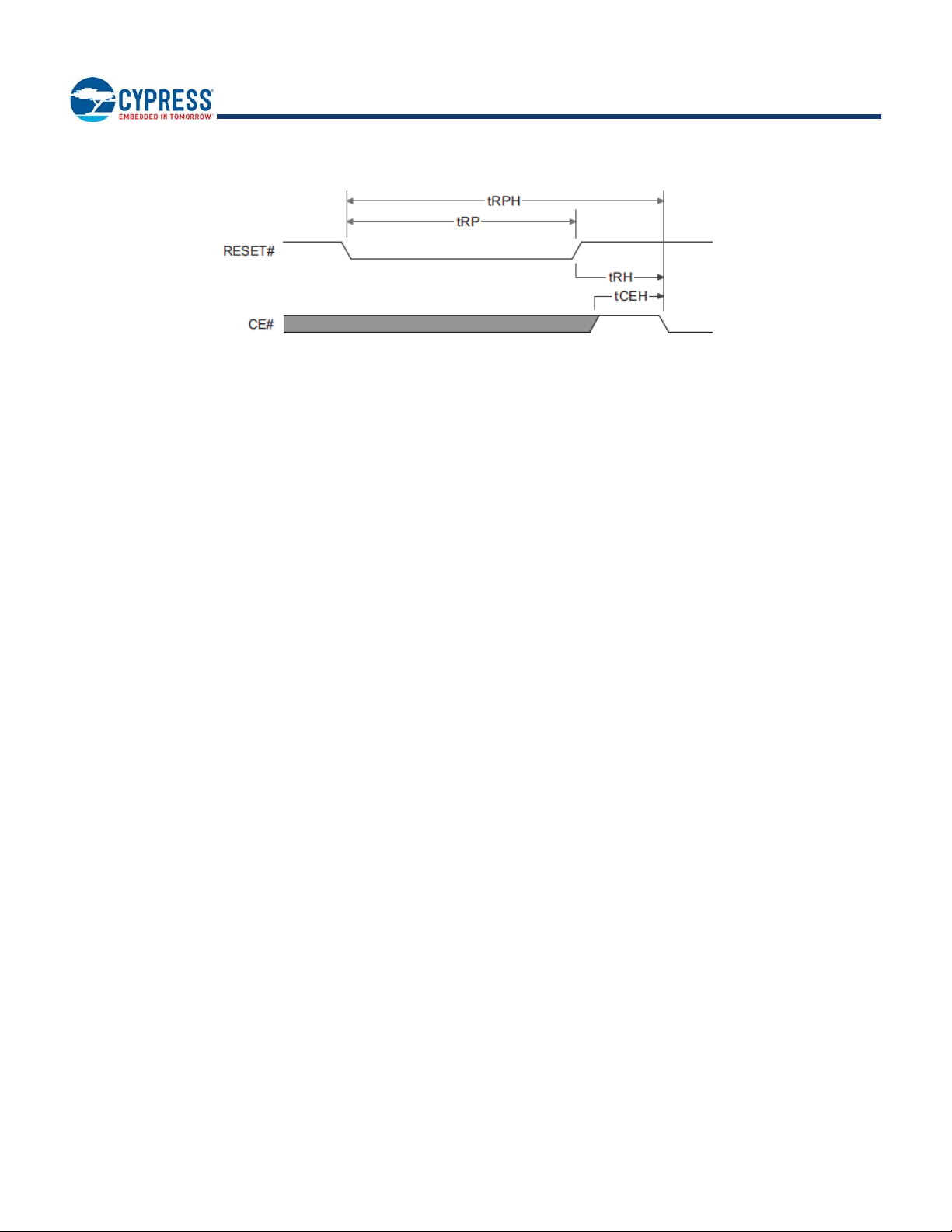
S29GL01GP
S29GL512P
S29GL256P
S29GL128P
Figure 13.2 Warm Reset Timing
Note:
The sum of t
The differences in power-on timing should not present a migration challenge for most applications where the flash interfaces directly
with a Host that requires oscillator and PLL lock prior to initiating the first boot read access to the flash. In applications which may
access the flash within 300 µs of power application, some circuit modification will be required to accommodate migration to GL-S
flash.
To initiate the first read or write cycle after power on, the GL-S requires CE# or OE# to transition from High to Low no sooner than
after VCC exceeds V
t
VCS
edge which initiates the first access.
CE# is ignored during Warm Reset; however, to initiate the first read or write cycle after warm reset, the GL-S requires CE# to
transition from High to Low no sooner than t
prior to CE# falling edge, which initiates first access. These were not requirements for the GL-P so designs that have CE# fixed low
cannot migrate to GL-S without modification to enable active CE# control.
The GL-S allows VIO to ramp concurrently with or after VCC with no restriction on time or voltage differential. During power ramp no
input is allowed to exceed VIO. The GL-S data sheet provides enhanced direction on power management and control to design a
robust and reliable system.
and tRH must be equal to or greater than t
RP
and VIO exceeds V
CC_min
RH
RPH.
. CE# or OE# must be High at least t
IO_min
after RESET# transitions from Low to High. CE# must be high at least t
= 20 ns prior to CE# or OE# falling
CEH
CEH
= 20 ns
Document Number: 002-00886 Rev. *B Page 77 of 83
Page 78

S29GL01GP
S29GL512P
S29GL256P
S29GL128P
14. Document History
Document Title:S29GL01GP, S29GL512P, S29GL256P, S29GL128P
1 Gbit, 512, 256, 128 Mbit, 3 V, Page Flash with 90 nm MirrorBit Process Technology
Document Number: 002-00886
Rev. ECN No.
** -
Orig. of
Change
RYSU
Submission
Date
10/29/2004 Spansion Publication Number: S29GL-P_00
A0:Initial release
10/20/2005
10/19/2006
11/21/2006 A3:AC Characteristics Erase and Program Operations table: Changed tBUSY to
12/18/2006
05/18/2007
A1:Global Revised all sections of document.
A2:Global
Revised all sections of document. Reformatted document to new template.
Changed speed options
for S29GL01GP
a maximum specification.
A4:Global
Changed tACC, tCE specifications on 128 Mb, 256 Mb, and 512 Mb devices.
Added 90 and 100 ns
speed options.
Write Buffer Programming, Sector Erase
Write Buffer Programming Operation, Sector Erase Operation figures:
Deleted “Wait 4 ms” box from
flowcharts.
Password Protection Method Lock Register Program Algorithm figure:
Deleted “Wait 4 ms” box from flowchart.
Read-only Operations table Modified tRC, tACC, tCE, tOE specifications.
Program and Erase Operations tables Changed tDS specification, deleted
write cycle time note.
TSOP Pin and BGA Capacitance table Changed all specifications in table.
A5:Global
Changed data sheet status to Preliminary.
Deleted references to requirement for external WP# pull-up.
Performance Characteristics Max. Read Access Times table: Added note.
Hardware Reset Deleted note from section.
AC Characteristics Reset Timings figure: Deleted note.
Command Definitions tables
S29GL-P Sector Protection Command Definitions tables: Changed “Global
Non-Volatile Freeze” to “Global Volatile Freeze”.
DC Characteristics CMOS Compatible table: Changed ICC1 maximum
current for 5 MHz and MHz test conditions.
Page Read Timings figure Corrected address range for top waveform
Description of Change
Document Number: 002-00886 Rev. *B Page 79 of 83
Page 79

S29GL01GP
S29GL512P
S29GL256P
S29GL128P
Document Title:S29GL01GP, S29GL512P, S29GL256P, S29GL128P
1 Gbit, 512, 256, 128 Mbit, 3 V, Page Flash with 90 nm MirrorBit Process Technology
Document Number: 002-00886
Rev. ECN No.
** - RYSU
Orig. of
Change
Submission
Date
10/23/2007
11/08/2007
11/28/2007
02/15/2008
03/19/2008
06/11/2008
Description of Change
A6:Performance Characteristics Changed speed options for S29GL512P
Ordering Information Corrected samples OPN valid combinations; changed
speed options for S29GL512P
64-Ball Fortified BGA Clarified ball “D1” connection
56-Pin TSOP Clarified pin “30” connection
Autoselect Added recommendation statement
Accelerated Program Added recommendation statement
Persistent Protection Bits Removed “Erase” from title and flow chart
Secured Silicon Sector
Sections “Factory Locked Secured Silicon Sector” & “Customer Lockable
Secured Silicon Sector”:
clarified shipping options
Power-up Sequence Timing Changed tRH from “Max” to “Min” value
Advance Information on S29GL-R 65 nm MirrorBit Hardware Reset
(RESET#) and Power-up Sequence
Added section
Global Fixed cross-references that were not live hyperlinks
A7:Advance Information on S29GL-R 65 nm MirrorBit Hardware Reset
(RESET#) and Power-up Sequence
Changed timing specs and waveforms
A8:Ordering Information New commercial operating temperature option
Operating Ranges New operating temperature range
A9:Electrical Specification Modified Test Conditions
Erase and Programming Performance Chip Program Time: removed
comment
Sector Protection Command Definition,x16 Table
Corrected Lock Register “Read” address
Advance Information on S29GL-R 65 nm MirrorBit Hardware Reset
(RESET#) and Power-up Sequence
Power-Up Sequence Timings Table: modified Note 2 - reduced timing from 500
μs to 300 μs
A10:Global Changed document status to Full Production.
DC Characteristics Changed Max values for Input Load Current (ILI)
Sector Protection Command Definitions
(x16 & x8 tables)
Changed Lock Register Read command from “DATA” to “RD”
A11:Ordering Information Revised Commercial temperature range
Figure: Write Operation Status
Flowchart
Updated flowchart
Document Number: 002-00886 Rev. *B Page 80 of 83
Page 80

S29GL01GP
S29GL512P
S29GL256P
S29GL128P
Document Title:S29GL01GP, S29GL512P, S29GL256P, S29GL128P
1 Gbit, 512, 256, 128 Mbit, 3 V, Page Flash with 90 nm MirrorBit Process Technology
Document Number: 002-00886
Rev. ECN No.
** - RYSU
Orig. of
Change
Submission
Date
11/20/2009
Description of Change
A12:Table Input/Output Descriptions Removed RFU description
Figure 64-ball Fortified Ball Grid Array Changed all RFU pins to NC pins
Figure 56-pin Standard TSOP (Top View)
Changed all RFU pins to NC pins
Table Autoselect Exit Changed cycle description to Auto Select Exit Command
Table Chip Erase Changed address of last C source code command from
0x000h to 0x555h
Erase Suspend/Erase Resume
Changed first paragraph, second sentence to sector address is “don't care”
for Erase Suspend
Changed sixth paragraph, second sentence to sector address is “don't care”
for Erase Suspend
Tables
Program Suspend
Program Resume
Unlock Bypass Entry
Unlock Bypass Program
Unlock Bypass Reset
Added Byte Address to tables
Unlock Bypass
Third paragraph, first sentence added unlock bypass Sector Erase and
unlock bypass Chip Erase
as valid commands
Changed paragraph, third sentence to sector address of exit command is
“don't care”.
Writing Commands/Command Sequence
Changed tables listed in fourth sentence to Table 6.1-6.4
WP#/ACC Method Changed table listed in Note section to 11.2.
Secured Silicon Sector Entry/Exit Command Sequence
Added source code for program under Table 10.3
Table Secured Silicon Sector Exit Changed Byte and Word addresses of
Exit Cycle to “XXXh”
Figure Test Setup Changed test setup to show only a load of CL
Table Test Specification Removed Output Load Test Condition
Table S29GL-P Erase and Program Operations
Removed tGHWL
Table S29GL-P Alternate CE# Contro lled Erase and Program
Operations
Changed description of tGHEL to (OE# High to CE# Low)
Change Note 2 to “DC Characteristics
TSOP Pin and BGA Package Capacitance
Changed RESET# values.
Document Number: 002-00886 Rev. *B Page 81 of 83
Page 81
S29GL01GP
S29GL512P
S29GL256P
S29GL128P
Document Title:S29GL01GP, S29GL512P, S29GL256P, S29GL128P
1 Gbit, 512, 256, 128 Mbit, 3 V, Page Flash with 90 nm MirrorBit Process Technology
Document Number: 002-00886
Rev. ECN No.
** - RYSU
*A 5051914 RYSU 12/16/2015 Updated to Cypress template
*B 5741254 AESATMP7 05/22/2017 Updated Cypress Logo and Copyright.
Orig. of
Change
Submission
Date
11/20/2008
11/17/2010
10/22/2012
Description of Change
Table S29GL-P Memory Array Command Definitions, x16
Changed number of cycles for Device ID to 6
Changed number of cycles for Write Buffer to 6
Added note regarding the number of cycles in a Write Buffer command
Table S29GL-P Memory Array Command Definitions, x8
Changed number of cycles for Device ID to 6
Changed number of cycles for Write Buffer to 6
Added note regarding the number of cycles in a Write Buffer command
Table System Interface String
Changed value of address 20h (x16) to 0009h and description to
“Typical timeout for buffer write 2n μs”
Added values of 128 Mb-512 Mb densities to address 22h (x16)
Table Device Geometry Definition For address 31h (x16) corrected x8 ad-
dress
A13:Performance Characteristics Updated access time options for
S29GL512P
Ordering Information Updated speed options for S29GL512P
Read Operation Timing Figure Added note
A14:Sector Erase Clarified tSEA
Erase Suspend Clarified tSEA
Writing Commands/Command Sequences
Sub-section RY/BY#: Clarified last sentence
Figure Advanced Sector Protection/Unprotection
Corrected Note numbering
Table S29GL-P Memory Array Command Definitions, x8
Corrected Address for 3rd Cycle of Write-To-Buffer-Abort Reset command
Table System Interface String Changed value of address 20h (x16) to
0006h
Advance Information on S29GL-R 65 nm MirrorBit Hardware Reset
(RESET#) and Power-up Sequence
Updated section title to Advance Information on S29GL-S Eclipse 65 nm
MirrorBit Power-On and
Warm Reset Timing
Updated section to cover GL-S Power-On and Warm Reset Timing
Document Number: 002-00886 Rev. *B Page 82 of 83
Page 82

S29GL01GP
S29GL512P
S29GL256P
S29GL128P
Sales, Solutions, and Legal Information
Worldwide Sales and Design Support
Cypress maintains a worldwide network of offices, solution centers, manufacturer’s representatives, and distributors. To find the office
closest to you, visit us at Cypress Locations.
Products
Automotive..................................cypress.com/go/automotive
Clocks & Buffers ................................ cypress.com/go/clocks
Interface......................................... cypress.com/go/interface
Lighting & Power Control............ cypress.com/go/powerpsoc
Memory........................................... cypress.com/go/memory
PSoC ....................................................cypress.com/go/psoc
Touch Sensing .................................... cypress.com/go/touch
USB Controllers....................................cypress.com/go/USB
Wireless/RF .................................... cypress.com/go/wireless
PSoC® Solutions
psoc.cypress.com/solutions
PSoC 1 | PSoC 3 | PSoC 4 | PSoC 5LP | PSoC 6
Cypress Developer Community
Community | Forums | Blogs | Video | Training
Technical Support
cypress.com/go/support
© Cypress Semiconductor Corporation, 2004-2017. This document is the property of Cypress Semiconductor Corporation and its subsidiaries, including Spansion LLC ("Cypress"). This document,
including any software or firmware included or referenced in this document ("Software"), is owned by Cypress under the intellectual property laws and treaties of the United States and other countries
worldwide. Cypress reserves all rights under such laws and treaties and does not, except as specifically stated in this paragraph, grant any license under its patents, copyrights, trademarks, or other
intellectual property r ights. If the Software is not accompanied by a li cense agreement and you do not otherwise have a wri tten agreement with Cypress governing the use of th e Software, then Cypress
hereby grants you a personal, non-exclusive, nontransferable license (without the right to sublicense) (1) under its copyright rights in the Software (a) for Software provided in source code form, to
modify and reproduce the Software solely for use with Cypress har dware products, only internally within your organization, and (b) to distribute the Software in binary code form externally to end users
(either directly or indirectly through resellers and distributors), solely for use on Cypress hardware product units, and (2) under those claims of Cypress's patents that are infringed by the Software (as
provided by Cypress, unmodified) to make, use, distribute, and import the Software solely for use with Cypress hardware products. Any other use, reproduction, modification, translation, or compilation
of the Software is prohibited.
TO THE EXTENT PERMITTED BY APPLICABLE LAW, CYPRESS MAKES NO WARRANTY OF ANY KIND, EXPRESS OR IMPLIED, WITH REGARD TO THIS DOCUMENT OR ANY SOFTWARE
OR ACCOMPANYING HARDWARE, INCLUDING, BUT NOT LIMITED TO, THE IMPLIED WARRANTIES OF MERCHANTABILITY AND FITNESS FOR A PARTICULAR PURPOSE. To the extent
permitted by applicable law, Cypress reserves the right to make changes to this document without further notice. Cypress does not assume any liability arising out of the application or use of any
product or circuit described in this document. Any information provided in this document, including any sample design information or programming code, is provided only for reference purposes. It is
the responsibility of the user of this document to properly design, progra m, and test the functionality and safety of any application made of this information and any resulting product. Cypress products
are not designed, intended, or authorized for use as critical components in systems designed or intended for the operation of weapons, weapons systems, nuclear installations, life-support devices or
systems, other medical devices or systems (including resuscitation equipment and surgical implants), pollution control or hazardous substances management, or other uses where the failure of the
device or system could cause personal injury, death, or property damage ("Unintended Uses"). A critical component is any component of a device or system whose failure to perform can be reasonably
expected to cause the failure of the device or system, or to affect its safety or effectiveness. Cypress is not liable, in whole or in part, and you shall and hereby do release Cypress from any claim,
Document Number: 002-00886 Rev.*B Revised May 22, 2017 Page 83 of 83
 Loading...