

Page 1

PSoC® CY8C24533, CY8C23533, CY8C23433 TRM
PSoC® CY8C24533, CY8C23533, CY8C23433
Technical Reference Manual (TRM)
Document # 001-20559 Rev. *D
January 19, 2017
Cypress Semiconductor
198 Champion Court
San Jose, CA 95134-1709
Phone (USA): 800.858.1810
Phone (Intnl.): 408.943.2600
http://www.cypress.com
Page 2

Copyrights
Copyrights
© Cypress Semiconductor Corporation, 2007-2017. This document is the property of Cypress Semiconductor Corporation
and its subsidiaries, including Spansion LLC ("Cypress"). This document, including any software or firmware included or referenced in this document ("Software"), is owned by Cypress under the intellectual property laws and treaties of the United
States and other countries worldwide. Cypress reserves all rights under such laws and treaties and does not, except as specifically stated in this paragraph, grant any license under its patents, copyrights, trademarks, or other intellectual property
rights. If the Software is not accompanied by a license agreement and you do not otherwise have a written agreement with
Cypress governing the use of the Software, then Cypress hereby grants you a personal, non-exclusive, nontransferable
license (without the right to sublicense) (1) under its copyright rights in the Software (a) for Software provided in source code
form, to modify and reproduce the Software solely for use with Cypress hardware products, only internally within your organization, and (b) to distribute the Software in binary code form externally to end users (either directly or indirectly through resellers and distributors), solely for use on Cypress hardware product units, and (2) under those claims of Cypress's patents that
are infringed by the Software (as provided by Cypress, unmodified) to make, use, distribute, and import the Software solely
for use with Cypress hardware products. Any other use, reproduction, modification, translation, or compilation of the Software
is prohibited.
TO THE EXTENT PERMITTED BY APPLICABLE LAW, CYPRESS MAKES NO WARRANTY OF ANY KIND, EXPRESS OR
IMPLIED, WITH REGARD TO THIS DOCUMENT OR ANY SOFTWARE OR ACCOMPANYING HARDWARE, INCLUDING,
BUT NOT LIMITED TO, THE IMPLIED WARRANTIES OF MERCHANTABILITY AND FITNESS FOR A PARTICULAR PURPOSE. To the extent permitted by applicable law, Cypress reserves the right to make changes to this document without further notice. Cypress does not assume any liability arising out of the application or use of any product or circuit described in
this document. Any information provided in this document, inclu ding any sample design info rmation o r progra mming co de, is
provided only for reference purposes. It is the responsibility of the user of this document to properly design, program, and test
the functionality and safety of any application made of this information and any resulting p roduct. Cypress products are not
designed, intended, or authorized for use as critical components in systems designed o r intended for the operation of we apons, weapons systems, nuclear installations, life-support devices or systems, other medical devices or systems (including
resuscitation equipment and surgical implants), pollution control or hazardous substances management, or other uses where
the failure of the device or system could cause personal injury, death, or property damage ("Unintended Uses"). A critical
component is any component of a device or system whose failure to perform can be reasonably expected to cause the failure
of the device or system, or to affect its safety or effectiveness. Cypress is not liable, in whole or in part, and you shall a nd
hereby do release Cypress from any claim, damage, or other liability arising from or related to all Unintended Uses of Cypress
products. You shall indemnify and hold Cypress harmless from and against all cla ims, costs, damages, and other liabilities,
including claims for personal injury or death, arising from or related to any Unintended Uses of Cypress products.
Cypress, the Cypress logo, Spansion, the Spansion logo, and combinations thereof, WICED, PSoC, CapSense, EZ-USB, FRAM, and Traveo are trademarks or registered trademarks of Cypress in the United States and other countries. For a more
complete list of Cypress trademarks, visit cypress.com. Other names and brands may be claimed as property of their respective owners.
2 Document # 001-20559 Rev. *D
Page 3

Contents Overview
Section A: Overview 17
1. Pin Information
Section B: PSoC Core 31
2. CPU Core (M8C)
3. Supervisory ROM (SROM)..... .............. ............. .............. ............. .............. ........... ...........45
4. RAM Paging............................................ ............. .............. .............. ............. .............. ......55
5. Interrupt Controller . .............. ............. ............ ............. .............. ............. .............. .............61
6. General Purpose IO (GPIO) ........................... ........... .............. ............. .............. .............69
7. Analog Output Drivers. ............. .............. ............. .............. .............. ........... .............. ........77
8. Internal Main Oscillator (IMO) ...................................... ............. .............. ............. ...........79
9. Internal Low Speed Oscillator (ILO). .............. .............. ........... ............. .............. .............83
10. External Crystal Oscillator (ECO)................................... ............. ............ ............. ...........85
11. Phase-Locked Loop (PLL) ............................ ............. ............ ............. .............. ............. ..91
12. Sleep and Watchdog ............................ ............. .............. ............. ............ ............. ...........95
............................ ............. ........... .............. .............. ............. .............. ......25
........................... ............. ............ ............. .............. ............. .............. ....35
Section C: Register Reference 107
13. Register Details
Section D: Digital System 225
14. Global Digital Interconnect (GDI)
15. Array Digital Interconnect (ADI) ............ ............. .............. .............. ............. .............. .... 233
16. Row Digital Interconnect (RDI) ............ ............. .............. ............. .............. .............. ...... 235
17. Digital Blocks ................... .............. ............. .............. .............. ............. ........... .............. .. 241
Section E: Analog System 279
18. Analog Interface
19. Analog Array ........................... .............. ............. .............. ........... .............. ............. ......... 297
20. Analog Input Configuration........... ............. .............. .............. ............. .............. ............. 305
21. Analog Reference.......... .............. ............. .............. ............. .............. ............. .............. .. 309
22. Continuous Time PSoC Block....... ............. .............. .............. ............. .............. ............. 313
23. Switched Capacitor PSoC Block ........... ............. .............. .............. ............. .............. .... 319
24. SAR8 ADC PSoC Block ....... ............. .............. .............. ............. ........... .............. ........... 329
Section F: System Resources 335
25. Digital Clocks
26. Multiply Accumulate (MAC) ... .............. ........... .............. ............. .............. ............. ......... 349
27. Decimator.................. .............. .............. ............. .............. ............. .............. ........... ......... 355
28. I2C ......................................... ............. .............. .............. ........... ............. .............. ........... 359
29. Internal Voltage Reference .................... ............. .............. .............. ............. .............. .... 375
30. System Resets................... .............. .............. ............. .............. ............. .............. ........... 377
31. POR and LVD ..... ............. .............. ............. .............. .............. ............. .............. ............. 383
........................... ............. ........... .............. .............. ............. .............. .....111
.......................... ............. ............ ............. .............. .... 229
.......................... ............. ........... .............. .............. ............. .............. .... 283
.......................... .............. ........... .............. ............. .............. ............. ......... 339
Document # 001-20559 Rev. *D 3
Page 4

Contents Overview
Section G: Glossary 385
Index 401
4 Document # 001-20559 Rev. *D
Page 5

Contents
Section A: Overview 17
Document Organization ......................................................................................................................17
Top-Level Architecture ................. ... ... ....................................... ... ... ... .... ... ... ... .... ... ... ..........................18
PSoC Core ................................................................................................................................18
Digital System ............................................................................................................................18
Analog System ................................................ ... .......................................................................18
System Resources ................................... ... .... ... ... ... .... ... ... ....................................... ... ... ... .......18
PSoC Device Characteristics ..............................................................................................................20
PSoC Device Distinctions ........................ .... ... ... .......................................... ... .... ................................20
Getting Started ...................................................................................................................................21
Support ......................................................................................................................................21
Product Upgrades ......................................................................................................................21
Development Kits .....................................................................................................................21
Document History ................................................................................................................................21
Documentation Conventions ..............................................................................................................22
Register Conventions ..............................................................................................................22
Numeric Naming .......................................................................................................................22
Units of Measure ....................................................................................................................22
Acronyms .............. ...................................... .... ... ... ... .... ... ... ....................................... ................23
1. Pin Information..................................................................................................................25
1.1 Pinouts ................................... ................................ ............................. .......................................25
1.1.1 28-Pin Part Pinout...... ... ... ....................................... ... .... ... ... ... .... ................................26
1.1.2 32-Pin Part Pinout...... ... ... ....................................... ... .... ... ... ... .... ................................28
1.1.3 56-Pin Part Pinout...... ... ... ....................................... ... .... ... ... ... .... ................................29
Section B: PSoC Core 31
Top-Level Core Architecture ................................................................................................................31
Interpreting Core Documentation ........................................ .................................................................31
Core Register Summary ......................................................................................................................32
2. CPU Core (M8C).................................................................................................................35
2.1 Overview ................................... ............................. ............................. .......................................35
2.2 Internal Registers ................................................... .... ... ..........................................................35
2.3 Address Spaces .......................................................................................................................35
2.4 Instruction Set Summary .............. ... .... ... ... ... .... ... ... ... .................................................................36
2.5 Instruction Formats ............... ... ... ... .... ... ... ... .... ..........................................................................38
2.5.1 One-Byte Instructions..................................................................................................38
2.5.2 Two-Byte Instructions................. ... .... ... ... ... .... .............................................................38
2.5.3 Three-Byte Instructions...............................................................................................39
2.6 Addressing Modes ....................................................................................................................39
2.6.1 Source Immediate.......................................................................................................39
2.6.2 Source Direct ..............................................................................................................40
2.6.3 Source Indexed...........................................................................................................40
Document # 001-20559 Rev. *D 5
Page 6

Contents Overview
2.6.4 Destination Direct .......................................................................................................41
2.6.5 Destination Indexed ...................................................................................................41
2.6.6 Destination Direct Source Immediate .................. .... ... ... ... ... .......................................41
2.6.7 Destination Indexed Source Immediate......................................................................42
2.6.8 Destination Direct Source Direct.... ... ... ... .... ... ... ... .... ... ... ... ... .......................................42
2.6.9 Source Indirect Post Increment ..................................................................................43
2.6.10 Destination Indirect Post Increment.................. ... .... ... ... ... ... .... ... ... ... ..........................43
2.7 Register Definitions ...................................................................................................................44
2.7.1 CPU_F Register .........................................................................................................44
3. Supervisory ROM (SROM)................................................................................................. 45
3.1 Architectural Description ...........................................................................................................45
3.1.1 Additional SROM Feature.............. ... ... ... .... ... ... ... .... ... ... .............................................46
3.1.2 SROM Function Descriptions ....................................................................................46
3.1.2.1 SWBootReset Function ............................................................................46
3.1.2.2 ReadBlock Function..................................... ... ... .... ... ... ... ..........................47
3.1.2.3 WriteBlock Function..................................................................................48
3.1.2.4 EraseBlock Function.......................................... .... ... ................................48
3.1.2.5 ProtectBlock Function...............................................................................49
3.1.2.6 TableRead Function ................................................................................49
3.1.2.7 EraseAll Function......................................................................................49
3.1.2.8 Checksum Function..................................................................................50
3.1.2.9 Calibrate0 Function...................................................................................50
3.1.2.10 Calibrate1 Function...................................................................................50
3.2 Register Definitions ..................................................................................................................51
3.2.1 CPU_SCR1 Register .................................................... ... ... .... ... ... ... .... ......................51
3.2.2 FLS_PR1 Register .....................................................................................................52
3.3 Clocking ....................................................................................................................................53
3.3.1 DELAY Parameter.......................................................................................................53
3.3.2 CLOCK Parameter......................................................................................................53
4. RAM Paging ...................................................................................................................... 55
4.1 Architectural Description ...........................................................................................................55
4.1.1 Basic Paging ..............................................................................................................55
4.1.2 Stack Operations .......................................................................................................56
4.1.3 Interrupts ............................................. ................................ ................................. ......56
4.1.4 MVI Instructions .........................................................................................................56
4.1.5 Current Page Pointer .................................................................... ... .... ... ...................56
4.1.6 Index Memory Page Pointer ............................ ... .... ... ... ... ..........................................57
4.2 Register Definitions ...................................................................................................................58
4.2.1 TMP_DRx Registers ..................................................................................................58
4.2.2 CPU_F Register..........................................................................................................59
5. Interrupt Controller........................................................................................................... 61
5.1 Architectural Description ............................................................................................................61
5.1.1 Posted versus Pending Interrupts...............................................................................62
5.2 Application Description ..............................................................................................................63
5.3 Register Definitions ...................................................................................................................64
5.3.1 INT_CLRx Registers ................. .... ... ... ... .... ... ... ... .... ... ................................................64
5.3.1.1 INT_CLR0 Register ..................................................................................64
5.3.1.2 INT_CLR1 Register ..................................................................................65
5.3.1.3 INT_CLR3 Register ..................................................................................65
5.3.2 INT_MSKx Registers .................................................................................................65
5.3.2.1 INT_MSK3 Register. .... .............................................................................65
6 Document # 001-20559 Rev. *D
Page 7

Contents Overview
5.3.2.2 INT_MSK0 Register.................................................................. ... ... ... .... ...66
5.3.2.3 INT_MSK1 Register.................................................................. ... ... ... .... ...66
5.3.3 INT_VC Register .... ... ... ... .... ... ... ... .... ... ... ... .... ... ... ... ... .... .......................................... ...66
5.3.4 CPU_F Register .........................................................................................................67
6. General Purpose IO (GPIO) ..................... ............. .............. .............. ............... .............. ....69
6.1 Architectural Description.............................................................................................................69
6.1.1 Digital IO ............. ... ... ... ... .... ...................................... .... ... ... ... ....................................69
6.1.2 Global IO ......... .... ... ... ... ... .... ...................................... .... ... ... ... .... ... .............................70
6.1.3 Analog Input ........... ... ... ....................................... ... ... .... ... ... ... ....................................70
6.1.4 GPIO Block Interrupts ...............................................................................................71
6.2 Register Definitions ...................................................................................................................72
6.2.1 PRTxDR Registers .....................................................................................................72
6.2.2 PRTxIE Registers .......................................................................................................72
6.2.3 PRTxGS Registers .....................................................................................................73
6.2.4 PRTxDMx Registers ................................................................................................74
6.2.5 PRTxICx Registers ............................ ... ... .................................................................75
7. Analog Output Drivers .......... .................. .................. ................ .................. ................ ......77
7.1 Architectural Description ............................................................................................................77
7.2 Register Definitions ..................................................................................................................78
7.2.1 ABF_CR0 Register .....................................................................................................78
8. Internal Main Oscillator (IMO) ............................ .............. ................ ............. .............. ......79
8.1 Architectural Description.............................................................................................................79
8.2 Application Description...............................................................................................................79
8.2.1 Trimming the IMO .......................................................................................................79
8.3 Register Definitions ...................................................................................................................80
8.3.1 CPU_SCR1 Register .................... .... ... ... ... .... .............................................................80
8.3.2 OSC_CR2 Register ....................................................................................................81
8.3.3 IMO_TR Register .......................................... ... ... ... ... .... ... ... ... .... ................................ 81
9. Internal Low Speed Oscillator (ILO)........................................ ............... .............. ............. 83
9.1 Architectural Description.............................................................................................................83
9.2 Register Definitions ...................................................................................................................83
9.2.1 ILO_TR Register ........................................................................................................83
10. External Crystal Oscillator (ECO) ........................... ................ ............. ................ ............. 85
10.1 Architectural Description.............................................................................................................85
10.1.1 ECO External Components.........................................................................................86
10.2 PSoC Device Distinctions...........................................................................................................86
10.3 Register Definitions ...................................................................................................................87
10.3.1 CPU_SCR1 Register ... ... .... ... ... ... .... ... ... ....................................................................87
10.3.2 OSC_CR0 Register ....................................................................................................88
10.3.3 ECO_TR Register ......................................................................................................89
11. Phase-Locked Loop (PLL) .................................................................................................91
11.1 Architectural Description.............................................................................................................91
11.2 Register Definitions ..................................................................................................................91
11.2.1 OSC_CR0 Register.....................................................................................................92
11.2.2 OSC_CR2 Register ....................................................................................................93
12. Sl eep and Watchdog .............. ................ ............. .............. ................ ............. .............. ......95
12.1 Architectural Description.............................................................................................................95
12.1.1 32 kHz Clock Selection ..............................................................................................95
Document # 001-20559 Rev. *D 7
Page 8

Contents Overview
12.1.2 Sleep Timer ..............................................................................................................95
12.2 Application Description...............................................................................................................96
12.3 Register Definitions ...................................................................................................................97
12.3.1 INT_MSK0 Register ...... ...................................................... ....................................... 97
12.3.2 RES_WDT Register ...................................................................................................97
12.3.3 CPU_SCR1 Register ................................................................................................98
12.3.4 CPU_SCR0 Register .................................................................................................99
12.3.5 OSC_CR0 Register .................................................................................................100
12.3.6 ILO_TR Register ......................................................................................................101
12.3.7 ECO_TR Register ....................................................................................................101
12.4 Timing Diagrams......................................................................................................................102
12.4.1 Sleep Sequence .......................................................................................................102
12.4.2 Wake Up Sequence.......................................................... ... .... ... ... ... ........................1 03
12.4.3 Bandgap Refresh......................................................................................................104
12.4.4 Watchdog Timer........................................................................................................104
12.5 Power Consumption.................................................................................................................105
Section C: Register Reference 107
Register General Conventions ...........................................................................................................107
Register Naming Conventions ...........................................................................................................107
Register Mapping Tables ...................................................................................................................107
Register Map Bank 0 Table: User Space ..... ... ... .... ... ... ... .... ... ... ... ... .... ... ..............................108
Register Map Bank 1 Table: Configuration Space ....................................... .... ... ... ... ... .... ... .109
13. Register Details................................................................................................................111
13.1 Maneuvering Around the Registers..........................................................................................111
Register Conventions ............................................................................................................112
13.1.1 Register Naming Conventions ................................................................................. 112
13.2 Bank 0 Registers .....................................................................................................................113
13.2.1 PRTxDR .... ....................... ...................... ....................... ....................... ....................113
13.2.2 PRTxIE ....................................................................................................................114
13.2.3 PRTxGS .... ....................... ...................... ....................... ....................... ....................115
13.2.4 PRTxDM2 ................................................................................................................ 116
13.2.5 DxBxxDR0 ............................................................................................................... 117
13.2.6 DxBxxDR1 ............................................................................................................... 118
13.2.7 DxBxxDR2 ............................................................................................................... 119
13.2.8 DxBxxCR0 (Timer Control) ...................................................................................... 120
13.2.9 DxBxxCR0 (Counter Control) ..................................................................................121
13.2.10 DxBxxCR0 (Dead Band Control) ............................................................................122
13.2.11 DxBxxCR0 (CRCPRS Control) ................................................................................123
13.2.12 DCBxxCR0 (SPIM Control) ......................................................................................124
13.2.13 DCBxxCR0 (SPIS Control) ................................................. .... ... ... ... .... ... ... ... ... .... ... .125
13.2.14 DCBxxCR0 (UART Transmit ter Control) .................................................................126
13.2.15 DCBxxCR0 (UART Receiver Control) .....................................................................127
13.2.16 AMX_IN ...................................................................................................................128
13.2.17 ARF_CR ..................................................................................................................129
13.2.18 CMP_CR0 ................................................................................................................130
13.2.19 ASY_CR .................................................................................... ..............................131
13.2.20 CMP_CR1 ................................................................................................................132
13.2.21 SARADC_DL ...........................................................................................................133
13.2.22 SARADC_CR0 .......... ...............................................................................................134
13.2.23 SARADC_CR1 .......... ...............................................................................................135
13.2.24 TMP_DRx ................................................................................................................ 136
8 Document # 001-20559 Rev. *D
Page 9

Contents Overview
13.2.25 ACBxxCR3 .......... .....................................................................................................137
13.2.26 ACBxxCR0 .......... .....................................................................................................138
13.2.27 ACBxxCR1 .......... .....................................................................................................140
13.2.28 ACBxxCR2 .......... .....................................................................................................142
13.2.29 ASDxxCR0 .......... ................................................................... ..................................143
13.2.30 ASDxxCR1 .......... ................................................................... ..................................144
13.2.31 ASDxxCR2 .......... ................................................................... ..................................145
13.2.32 ASDxxCR3 .......... ................................................................... ..................................146
13.2.33 ASCxxCR0 .......... ................................................................... ..................................147
13.2.34 ASCxxCR1 .......... ................................................................... ..................................148
13.2.35 ASCxxCR2 .......... ................................................................... ..................................149
13.2.36 ASCxxCR3 .......... ................................................................... ..................................150
13.2.37 RDIxRI ....... ...... ....... ...... ....... ...... ....... ...... ....... ...... ... ....... ...... ....... ...... ...... ....... ...........151
13.2.38 RDIxSYN ...... .................................... ................................... .....................................152
13.2.39 RDIxIS .......... ....................................... .......................................... ...........................153
13.2.40 RDIxLT0 .......... .........................................................................................................154
13.2.41 RDIxLT1 .......... .........................................................................................................155
13.2.42 RDIxRO0 ... ................................... ....................................... .....................................156
13.2.43 RDIxRO1 ... ................................... ....................................... .....................................157
13.2.44 I2C_CFG ............. ....................................................................... ..............................158
13.2.45 I2C_SCR ............. ....................................................................... ..............................159
13.2.46 I2C_DR ....................................................................................................................161
13.2.47 I2C_MSCR .......... ................................................................... ..................................162
13.2.48 INT_CLR0 ................................................................................................................163
13.2.49 INT_CLR1 ................................................................................................................165
13.2.50 INT_CLR3 ................................................................................................................166
13.2.51 INT_MSK3 .............. ...... ............................................................................................167
13.2.52 INT_MSK0 .............. ...... ............................................................................................168
13.2.53 INT_MSK1 .............. ...... ............................................................................................169
13.2.54 INT_VC ....................................................................................................................170
13.2.55 RES_WDT ....... .... ...... ...... ....... ...... ....... ...... ....... ...... ....... ...... ....... ...... ...... ....... ...... ..... 171
13.2.56 DEC_DH ..................................................................................................................172
13.2.57 DEC_DL ..................................................................................................................173
13.2.58 DEC_CR0 ............................................................................. .... ... ... ... ... .... ... ... ... .... .174
13.2.59 DEC_CR1 ................................................................................................................175
13.2.60 MULx_X ...................................................................................................................176
13.2.61 MULx_Y ...................................................................................................................177
13.2.62 MULx_DH ..... ....... ...... ...... .... ...... ....... ...... ....... ...... ...... ....... ...... ....... ...... ....... ...... ........178
13.2.63 MULx_DL .................................................................................................................179
13.2.64 MACx_X/ACCx_DR1 ...............................................................................................180
13.2.65 MACx_Y/ACCx_DR0 ...............................................................................................181
13.2.66 MACx_CL0/ACCx_DR3 ...........................................................................................182
13.2.67 MACx_CL1/ACCx_DR2 ...........................................................................................183
13.2.68 CPU_F ................................................................................................................184
13.2.69 CPU_SCR1 .........................................................................................................185
13.2.70 CPU_SCR0 .. .................................................................... ........................................1
86
13.3 Bank 1 Registers ...................... ... ... .... ... ..................................................................................187
13.3.1 PRTxDM0 ........ ....... ...... ....... ... ...... ....... ...... ....... ...... ....... ...... ....... ...... ...... ....... ...... ..... 187
13.3.2 PRTxDM1 ........ ....... ...... ....... ... ...... ....... ...... ....... ...... ....... ...... ....... ...... ...... ....... ...... ..... 188
13.3.3 PRTxIC0 ....... ... ....... ...... ....... ...... ....... ...... ....... ...... ...... ....... ...... ....... ...... ....... ...... ........189
13.3.4 PRTxIC1 ....... ... ....... ...... ....... ...... ....... ...... ....... ...... ...... ....... ...... ....... ...... ....... ...... ........190
13.3.5 DxBxxFN ...... ....................................................................... .....................................191
13.3.6 DxBxxIN ...................................................................................................................193
Document # 001-20559 Rev. *D 9
Page 10

Contents Overview
13.3.7 DxBxxOU ................................................................................................................. 195
13.3.8 CLK_CR0 ..... ....................... .......................... ...................... ....................... ..............197
13.3.9 CLK_CR1 ..... ....................... .......................... ...................... ....................... ..............198
13.3.10 ABF_CR0 .............................................................................................................199
13.3.11 AMD_CR0 ........... .....................................................................................................200
13.3.12 AMD_CR1 ........... .....................................................................................................201
13.3.13 ALT_CR0 .................................................................................................................202
13.3.14 SARADC_TRS . ............................. .......................... ......................... ........................203
13.3.15 SARADC_TRCL ......................................................................................................204
13.3.16 SARADC_TRCH . .......................................................... ........................................... 205
13.3.17 SARADC_CR2 .......... ...............................................................................................206
13.3.18 SARADC_LCR .... .......................... .......................... ......................... ........................207
13.3.19 GDI_O_IN ................................................................................................................208
13.3.20 GDI_E_IN ................................................................................................................209
13.3.21 GDI_O_OU .............................................................................................................. 210
13.3.22 GDI_E_OU ....... ......................... .......................... .......................... ...........................211
13.3.23 OSC_GO_EN ..........................................................................................................212
13.3.24 OSC_CR4 . .................................................... ....................................................... .... 213
13.3.25 OSC_CR3 . .................................................... ....................................................... .... 214
13.3.26 OSC_CR0 ............................................................................................................215
13.3.27 OSC_CR1 . .................................................... ....................................................... .... 216
13.3.28 OSC_CR2 ...............................................................................................................217
13.3.29 VLT_CR ...................................................................................................................218
13.3.30 VLT_CMP ................................................................................................................219
13.3.31 IMO_TR ...................................................................................................................220
13.3.32 ILO_TR ....................................................................................................................221
13.3.33 BDG_TR .................................................................................................................222
13.3.34 ECO_TR ..................................................................................................................223
13.3.35 FLS_PR1 ................................................................................................................224
Section D: Digital System 225
Top-Level Digital Architecture ...........................................................................................................225
Interpreting the Digital Documentation .............................................................................................225
Digital Register Summary .................................................................................................................226
14. G lobal Digital Interconnect (GDI) ..... .............. ............... .............. ................ ............. ....... 229
14.1 Architectural Description .........................................................................................................229
14.1.1 28-Pin Global Interconnect .....................................................................................230
14.2 Register Definitions .................................................................................................................231
14.2.1 GDI_x_IN Registers ...............................................................................................231
14.2.2 GDI_x_OU Registers ............................................................................................... 232
15. Array Digital Interconnect (ADI) ............................... ...................................................... 233
15.1 Architectural Description ..........................................................................................................233
16. Row Digital Interconnect (RDI) ................. .............. ............. ................ .............. ............. 235
16.1 Architectural Description ..........................................................................................................235
16.2 Register Definitions .................................................................................................................237
16.2.1 RDIxRI Register .......................................................................................................237
16.2.2 RDIxSYN Register ........................... ........................................................................237
16.2.3 RDIxIS Register ............................ ...........................................................................238
16.2.4 RDIxLTx Registers .................................................................................................239
16.2.5 RDIxROx Registers ...............................................................................................240
16.2.5.1 RDIxRO0 Register..................................................................................240
10 Document # 001-20559 Rev. *D
Page 11

Contents Overview
16.2.5.2 RDIxRO1 Register..................................................................................240
16.3 Timing Diagram ......................................................................................................................240
17. Digital Blocks ..................................................................................................................241
17.1 Architectural Description...........................................................................................................241
17.1.1 Input Multiplexers ......... .................................................................... ........................242
17.1.2 Input Clock Resynchronization ............ ...... ....... ...... ....... ...... ....... ...... ...... .... ...... ....... . 242
17.1.2.1 Clock Resynchronization Summary........................................................243
17.1.3 Output De-Multiplexers ............................................................................................243
17.1.4 Block Chaining Signals ............................................................................................243
17.1.5 Input Data Synchronization.......................................................................................243
17.1.6 Timer Function .................... .....................................................................................243
17.1.6.1 Usability Exceptions................................................................................243
17.1.6.2 Block Interrupt.............................. ... ... ... ... .... ... ... ... .... ... ... ... ... .... ... ... ... .....243
17.1.7 Counter Function ......................................................................................................244
17.1.7.1 Usability Exceptions................................................................................244
17.1.7.2 Block Interrupt.............................. ... ... ... ... .... ... ... ... .... ... ... ... ... .... ... ... ... .....244
17.1.8 Dead Band Function ................................................................................................244
17.1.8.1 Usability Exceptions................................................................................245
17.1.8.2 Block Interrupt.............................. ... ... ... ... .... ... ... ... .... ... ... ... ... .... ... ... ... .....245
17.1.9 CRCPRS Function ...................................................................................................245
17.1.9.1 Usability Exceptions................................................................................246
17.1.9.2 Block Interrupt.............................. ... ... ... ... .... ... ... ... .... ... ... ... ... .... ... ... ... .....246
17.1.10 SPI Protocol Function ................................................... ... ... ... .... ... ...........................247
17.1.10.1 SPI Protocol Signal Definitions...............................................................247
17.1.11 SPI Master Function ............................... ....... ...... ...... ....... ...... ....... ...... ....... ...... ... .....247
17.1.11.1 Usability Exceptions.................................................................. ... ... ... .... .248
17.1.11.2 Block Interrupt.................................................................... ... .... ... ... ... .....248
17.1.12 SPI Slave Function .... ... ... .... ... .......................................... ... ... .................................. 2 48
17.1.12.1 Usability Exceptions.................................................................. ... ... ... .... .248
17.1.12.2 Block Interrupt.................................................................... ... .... ... ... ... .....248
17.1.13 Asynchronous Transmitter and Receiver Functions .............................................249
17.1.13.1 Asynchronous Transmitter Function ......................... ... ... ... ... .... ... ... ... .... .249
17.1.13.2 Usability Exceptions.................................................................. ... ... ... .... .249
17.1.13.3 Block Interrupt.................................................................... ... .... ... ... ... .....249
17.1.13.4 Asynchronous Receiver Function ...........................................................249
17.1.13.5 Usability Exceptions.................................................................. ... ... ... .... .250
17.1.13.6 Block Interrupt.................................................................... ... .... ... ... ... .....250
17.2 Register Definitions .................................................................................................................251
17.2.1 DxBxxDRx Registers ................................................................................................252
17.2.1.1 Timer Register Definitions.......................................................................252
17.2.1.2 Counter Register Definitions...................................................................253
17.2.1.3 Dead Band Register Definitions..............................................................253
17.2.1.4 CRCPRS Register Definitions.................................................................254
17.2.1.5 SPI Master Register Definitions..............................................................254
17.2.1.6 SPI Slave Register Definitions................................................................255
17.2.1.7 Transmitter Register Definitions..............................................................255
17.2.1.8 Receiver Register Definitions..................................................................255
17.2.2 DxBxxCR0 Regist er ............ ... ... ... .... ... ... ... .... ... ... ... ... .......................................... .... .256
17.2.3 INT_MSK1 Register ...............................................................................................257
17.2.4 DxBxxFN Registers ..................................................................................................257
17.2.5 DxBxxIN Registers ...................................................................................................259
17.2.6 DxBxxOU Registers .................................................................................................260
Document # 001-20559 Rev. *D 11
Page 12

Contents Overview
17.3 Timing Diagrams .....................................................................................................................262
17.3.1 Timer Timing .............................................................. ... ... ... .... ... ... ... ........................262
17.3.2 Counter Timing ... ... ... ...............................................................................................263
17.3.3 Dead Band Timing ...................................................................................................264
17.3.3.1 Changing the PWM Duty Cycle..............................................................264
17.3.3.2 Kill Operation..........................................................................................265
17.3.4 CRCPRS Timing ......................................................................................................266
17.3.5 SPI Mode Timing .......................................................... ... ... .... .................................266
17.3.6 SPIM Timing ............................................................................................................267
17.3.7 SPIS Timing ............................................................... ... ... ... .... ... ... ...........................270
17.3.8 Transmitter Timing ...................................................................................................273
17.3.9 Receiver Timing .......................................................................................................275
Section E: Analog System 279
Top-Level Analog Architecture ........ ... .... ... ... .......................................... ... ... .... ... ... ... .... ....................279
Interpreting the Analog Documentation ............................................................................................279
Application Description ......................................................................................................................280
Defining the Analog Blocks .....................................................................................................280
Analog Functionality .................................................................. ... ... ... .... ... ... ... .... ... ... ... ...........280
Analog Register Summary .. ... ............................................................................................................281
18. Analog Interface.............................................................................................................. 283
18.1 Architectural Description .........................................................................................................283
18.1.1 Analog Data Bus Interface .................. ............................................................. ........2 84
18.1.2 Analog Comparator Bus Interface ............................................................................284
18.1.3 Analog Column Clock Generation ...........................................................................285
18.1.3.1 Column Clock Synchronization...............................................................285
18.1.4 Decimator and Incremental ADC Interface ..............................................................285
18.1.4.1 Decimator ...............................................................................................285
18.1.4.2 Incremental ADC ...................................................................................285
18.1.5 Analog Modulator Interface (Mod Bits) ....................................................................286
18.1.6 Analog Synchronization Interface (Stalling) ............................................................. 286
18.2 PSoC Device Distinctions.........................................................................................................286
18.3 Application Description.............................................................................................................286
18.3.1 SAR Hardware Acceleration .................................................................................... 286
18.3.1.1 Architectural Description.........................................................................287
18.3.1.2 Application Description...........................................................................287
18.3.1.3 SAR Timing..................................... ... .... ... ... ... ... .....................................290
18.4 Register Definitions .................................................................................................................291
18.4.1 CMP_CR0 Register ...............................................................................................291
18.4.2 ASY_CR Register ....................................................................................................291
18.4.3 CMP_CR1 Register .................................................................................................292
18.4.4 DEC_CR0 Regist er ................... .... ... ... ... .... ... ....................................... ... ... ... ... .... ... .293
18.4.5 DEC_CR1 Regist er ................... .... ... ... ... .... ... ....................................... ... ... ... ... .... ... .293
18.4.6 CLK_CR0 Register ..................................................................................................294
18.4.7 CLK_CR1 Register ..................................................................................................294
18.4.8 AMD_CR0 Register .................................................................................................295
18.4.9 AMD_CR1 Register .................................................................................................295
18.4.10 ALT_CR0 Register ...................................................................................................295
19. Analog Array ................................................................................................................... 297
19.1 Architectural Description ..........................................................................................................297
19.1.1 NMux Connections General Overview......................................................................298
12 Document # 001-20559 Rev. *D
Page 13

Contents Overview
19.1.2 PMux Connections General Overview ......................................................................299
19.1.3 RBotMux Connections General Overview.................................................................300
19.1.4 AMux Connections General Overview .....................................................................301
19.1.5 CMux Connections General Overview......................................................................302
19.1.6 BMux SC/SD Connections General Overview..........................................................303
19.1.7 Analog Comparator Bus ...........................................................................................303
19.2 Temperature Sensing Capability .............................................................................................303
20. Analog Input Configuration............................................................................................. 305
20.1 Architectural Description...........................................................................................................305
20.1.1 Two Column Analog Input Configuration........................................ ... ... ... .... ... ... ... .... .306
20.2 Register Definitions ................................................................................................................307
20.2.1 AMX_IN Register .....................................................................................................307
20.2.2 ABF_CR0 Register ...................................................................................................307
21. Analog Reference............................................................................................................309
21.1 Architectural Description...........................................................................................................309
21.2 Register Definitions .................................................................................................................310
21.2.1 ARF_CR Register ............................................ ... ... ... .... ... ... ... .... ... ... ... ... ..................310
22. Continuous Time PSoC Block ......................................................................................... 313
22.1 Architectural Description ..........................................................................................................313
22.2 Register Definitions .................................................................................................................315
22.2.1 ACBxxCR3 Register .................................................................................................315
22.2.2 ACBxxCR0 Register .................................................................................................317
22.2.3 ACBxxCR1 Register .................................................................................................317
22.2.4 ACBxxCR2 Register .................................................................................................318
23. Switched Capacitor PSoC Block .................................... .................. .................. ............. 319
23.1 Architectural Description...........................................................................................................319
23.2 Application Description.............................................................................................................321
23.3 Register Definitions .................................................................................................................322
23.3.1 ASCxxCR0 Register .................................................................................................323
23.3.2 ASCxxCR1 Register .................................................................................................324
23.3.3 ASCxxCR2 Register .................................................................................................324
23.3.4 ASCxxCR3 Register .................................................................................................325
23.3.5 ASDxxCR0 Register .................................................................................................326
23.3.6 ASDxxCR1 Register .................................................................................................327
23.3.7 ASDxxCR2 Register .................................................................................................327
23.3.8 ASDxxCR3 Register .................................................................................................328
24. SAR 8 ADC PSoC Block .................... .............. ............. .............. ............. ................ ......... 329
24.1 Architectural Description...........................................................................................................329
24.1.1 Features....................................................................................................................329
24.2 Register Definitions .................................................................................................................330
24.2.1 SARADC_DL Register .............................................................................................330
24.2.2 SARADC_CR0 Register ...........................................................................................330
24.2.3 SARADC_CR1 Register ...........................................................................................331
24.2.4 SARADC_TRS Register ...........................................................................................332
24.2.5 SARADC_TRCL Register ........................................................................................333
24.2.6 SARADC_TRCH Regist er ...... ... ... .... ... ... ... .... ... ... ... ... .... .......................................... .333
24.2.7 SARADC_CR2 Register ...........................................................................................334
24.2.8 SARADC_LCR Register ...........................................................................................334
Document # 001-20559 Rev. *D 13
Page 14

Contents Overview
Section F: System Resources 335
Top-Level System Resources Architecture .......................................................................................335
Interpreting the System Resources Documentation .........................................................................335
System Resources Register Summary ..............................................................................................336
25. Digital Clocks.................................................................................................................. 339
25.1 Architectural Description ..........................................................................................................339
25.1.1 Internal Main Oscillator ............................................................................................339
25.1.2 Internal Low Speed Oscillator .................................................................................. 339
25.1.3 32.768 kHz Crystal Oscillator............... .....................................................................341
25.1.4 External Clock ........................................................................................................341
25.1.4.1 Clock Doubler.........................................................................................341
25.1.4.2 Switch Operation .................. .... ... ...........................................................341
25.2 PSoC Device Distinctions.........................................................................................................342
25.3 Register Definitions .................................................................................................................343
25.3.1 INT_CLR0 Register .................................................................................................343
25.3.2 INT_MSK0 Register ...... ...................................................... ..................................... 343
25.3.3 OSC_GO_EN Register ............................................................................................344
25.3.4 OSC_CR4 Register .................................................................................................344
25.3.5 OSC_CR3 Register .................................................................................................345
25.3.6 OSC_CR0 Register ...............................................................................................346
25.3.7 OSC_CR1 Register .................................................................................................347
25.3.8 OSC_CR2 Register ...............................................................................................348
26. Mult iply Accumulate (MAC) ...... ................ ................ .................. ................ ................ .... 349
26.1 Architectural Description .........................................................................................................349
26.2 Application Description.............................................................................................................350
26.2.1 Multiplication with No Accumulation ........................................................................350
26.2.2 Accumulation After Multiplication..............................................................................350
26.3 Register Definitions .................................................................................................................351
26.3.1 MULx_X Register .....................................................................................................351
26.3.2 MULx_Y Register .....................................................................................................351
26.3.3 MULx_DH Register ..................................................................................................352
26.3.4 MULx_DL Register ....................... ... ... .....................................................................352
26.3.5 MACx_X/ACCx_DR1 Register ...... .......................... ......................... ........................352
26.3.6 MACx_Y/ACCx_DR0 Register ...... .......................... ......................... ........................353
26.3.7 MACx_CL0/ACCx_DR3 Regis ter .............. ..............................................................353
26.3.8 MACx_CL1/ACCx_DR2 Regis ter .............. ..............................................................353
27. Decimator........................................................................................................................ 355
27.1 Architectural Description ..........................................................................................................355
27.1.1 Decimator Block .......................................................................................................355
27.2 Register Definitions .................................................................................................................357
27.2.1 DEC_DH Register ....................................................................................................357
27.2.2 DEC_DL Register ....................................................................................................357
27.2.3 DEC_CR0 Regist er ................... .... ... ... ... .... ... ....................................... ... ... ... ... .... ... .358
27.2.4 DEC_CR1 Regist er ................... .... ... ... ... .... ... ....................................... ... ... ... ... .... ... .358
28. I2C ............................................................................................................................... .... 359
28.1 Architectural Description ..........................................................................................................359
28.1.1 Basic I2C Data Transfer............................................................................................359
28.2 Application Description.............................................................................................................360
28.2.1 Slave Operation .................................. ... .... ... ... .......................................... ... ... ........360
28.2.2 Master Operation .....................................................................................................361
14 Document # 001-20559 Rev. *D
Page 15

Contents Overview
28.3 Register Definitions .................................................................................................................362
28.3.1 I2C_CFG Register ..... ...... ....... ...... ....... ...... ....... ... ...... ....... ...... ....... ...... ....... ...... ....... . 362
28.3.2 I2C_SCR Register ....................................................................................................364
28.3.3 I2C_DR Register ......................................................................................................366
28.3.4 I2C_MSCR Register .................................................................................................366
28.4 Timing Diagrams ......................................................................................................................368
28.4.1 Clock Generation ......................................................................................................368
28.4.2 Basic Input/Output Timing.........................................................................................368
28.4.3 Status Timing ............................................................................................................369
28.4.4 Master Start Timing...................................................................................................370
28.4.5 Master Restart Timing...............................................................................................371
28.4.6 Master Stop Timing ..................................................................................................371
28.4.7 Master/Slave Stall Timing ........................................................... .............................. 372
28.4.8 Master Lost Arbitration Timing .................................................................................372
28.4.9 Master Clock Synchronization...................................................................................373
29. Inte rnal Voltage Reference............................................... ............. .............. ........... ......... 375
29.1 Architectural Description...........................................................................................................375
29.2 Register Definitions .................................................................................................................376
29.2.1 BDG_TR Register ....................................................................................................376
30. System Resets................................................................................................................. 377
30.1 Architectural Description...........................................................................................................377
30.2 Pin Behavior During Reset .......................................................................................................377
30.2.1 GPIO Behavior on Power Up ....................................................................................377
30.3 Register Definitions .................................................................................................................378
30.3.1 CPU_SCR1 Register .. ... .... ... ... ... .... ........................................................................378
30.3.2 CPU_SCR0 Register . ... ... .... ... ... ... .... ... ... ..................................................................379
30.4 Timing Diagrams .....................................................................................................................380
30.4.1 Power On Reset .......................................................................................................380
30.4.2 Watchdog Timer Reset .............................................................................................380
30.4.3 Reset Details.............................................................................................................382
30.5 Power Consumption ................................................................................................................382
31. POR and LVD .................. ................ ................ ................ .................. ............... ................ 383
31.1 Architectural Description...........................................................................................................383
31.2 Register Definitions .................................................................................................................384
31.2.1 VLT_CR Register ................................................... ... .... ... ........................................384
31.2.2 VLT_CMP Register ..................................................................................................384
Section G: Glossary 385
Index 401
Document # 001-20559 Rev. *D 15
Page 16

Contents Overview
16 Document # 001-20559 Rev. *D
Page 17

Section A: Overview
The PSoC® family consists of programmable system-on-chips with on-chip controller devices. As described in this technical
reference manual (TRM), a PSoC device includes configurable blocks of analog circuits and digital logic, as well as programmable interconnect. This architecture allows the user to create customized peripheral configurations, to match the
requirements of each individual application. Additionally, a fast CPU, Flash program memory, SRAM data memory, and configurable input/output (IO) are included in a range of pinouts.
This document is a technical reference manual for the PSoC device: CY8C24533, CY8C23533, CY8C23433CY8C24633. For
the most up-to-date Ordering, Pinout, Packaging, or Electrical Specification inf ormation, refer to the PSoC data sheet. For the
most current technical reference manual information, refer to the addendum. To obtain the newest product documentation, go
to the Cypress web site at http://www.cypress.com/psoc. This section encompasses the following chapter:
■ Pin Information on page 25
Document Organization
This manual is organized into sections and chap ters, according to PSoC functionali ty. Each section begins with documentation interpretation, a top-level architectural explanation, PSoC device distinctions (if relevant), and a register summary (if
applicable). Most chapters within the sections have an introduction, an architectural/application description, PSoC device distinctions (if relevant), register definitions, and timing diagrams. The sections are as follows:
■ Overview – Presents the PSoC top-level architecture, PSoC device characteristics and distinctions, how to get started
with helpful information, and document history and conventions. The PSoC device pinouts are detailed in the Pin
Information chapter on page 25.
■ PSoC Core – Describes the heart of the PSoC device in various chapters, beginning with an architectural overview and a
summary list of registers pertaining to the PSoC core. See “PSoC Core” on page 31.
■ Register Reference – Lists all PSoC device registers in Register Mapping Tables, on page 43, and presents bit-level
detail of each PSoC register in its own Register Details chapter on page 47. Where applicable, detailed register descriptions are also located in each chapter.
■ Digital System – Describes the configurable PSoC digital system in various chapters, beginning with an architectural
overview and a summary list of registers pertaining to the digital system. See the “Digital System” on page 161.
■ Analog System – Describes the configurable PSoC analog system in various chapters, beginning with an architectural
overview and a summary list of registers pertaining to the analog system. See the “Analog System ” on page 215.
■ System Resources – Presents additional PSoC system resources, depending on the PSoC device, beginning with an
overview and a summary list of registers pertaining to system resources. See “System Resources” on page 271.
■ Glossary – Defines the specialized terminology used in this manual. Glossary terms are presented in bold, italic font
throughout this manual. See the “Glossary” on page 321.
■ Index – Lists the location of key topics and elements that constitute and empower the PSoC device. See the “Index” on
page 401.
Document # 001-20559 Rev. *D 17
Page 18

Section A: Overview
Top-Level Architecture
The PSoC block diagram on the next page illustrates the
top-level architecture of the PSoC device. Each major
grouping in the diagram is covered in this manual in its own
section: PSoC Core, Digital System, Analog System, and
the System Resources. Banding these four main areas
together is the communication network of the system bus.
PSoC Core
The PSoC Core is a powerful engine that supports a rich
instruction set. It encompasses the SRAM for data storage,
an interrupt controller fo r easy program execution to new
addresses, sleep and watchdog timers, and multiple clock
sources that include the phase locked loop (PLL), IMO
(internal main oscillator), ILO (internal low speed oscillator),
and ECO (32.768 kHz external crystal oscillator) for precision, programmable clocking. The clocks, together with programmable clock dividers (as a System Resource), provide
the flexibility to integrate almost any timing requirement into
the PSoC device.
The CPU core, called the M8C, is a powerful processor with
speeds up to 24 MHz. The M8C is a four MIPS 8-bit Harvard architecture microprocessor. Within the CPU core are
the SROM and Flash memory components that provide
flexible programming.
PSoC GPIOs provide connection to the CPU, digital and
analog resources of the device. Each pin’s drive mode may
be selected from eight options, allowing great flexibility in
external interfacing. Every pin also has the capability to generate a system interrupt on high level, low level, and change
from last read.
Digital System
The Digital System is composed of digital rows in a block
array, and the Global, Array, and Row Digital Interconnects
(GDI, ADI, and RDI, respectively).The digital system block is
composed of 4 digital PSoC blocks. Each block is an 8-bit
resource that can be used alone or combined with other
blocks to form 8-, 16-, 24-, and 32-bit peripherals, which are
called user modules.
Analog System
The Analog System is composed of analog columns in a
block array, analog references, analog input muxing, and
analog drivers. The analog system block is composed of 6
configurable blocks, each comprised of an opamp circuit
allowing the creation of complex analog signal flows.
Analog blocks are arranged in a column of three, which
includes one CT (Continuous Time) and two SC (Switched
Capacitor) blocks. The Analog Column 0 contains the SAR8
ADC block rather than the standard SC blocks.
System Resources
The System Resources provide additional PSoC capability.
These system resources include:
■ Digital clocks to increase the flexibility of the PSoC
device.
■ One multiply accumulate (MAC) provides a fast 8-bit
multiplier with 32-bit accumulate to assist in both general
math as well as digital filters.
■ The decimator provides a custom hardware filter for digi-
tal signal processing applications, including the creation
of Delta Sigma ADCs.
■ I2C functionality for implementing either I2C slave or
master.
■ Low Voltage Detection (LVD) interrupts can signal the
application of falling voltage levels, while the advanced
POR (Power On Reset) circuit eliminates the need for a
system supervisor.
■ An internal voltage reference that provides an absolute
value of 1.3 V to a variety of PSoC subsystems.
■ Various system resets supported by the M8C.
The digital blocks can be connected to any GPIO through a
series of global buses that can route any signal to any p in.
The buses also allow for signal multiplexing and for performing logic operations. This configurability frees your designs
from the constraints of a fixed peripheral controller.
18 Document # 001-20559 Rev. *D
Page 19

PSoC Top-Level Block Diagram
DIGITAL SYSTEM
SRAM
256 Bytes
Interrupt
Controller
Sleep and
Watchdog
Multiple Clock Sources
(Includes IMO, ILO, PLL, and ECO)
Global Digital Interconnect
Global Analog Interconnect
PSoC CORE
CPU Core (M8C)
SROM Flash 8K
Multiply
Accum.
(MAC)
Internal
Voltage
Ref.
Digital
Clocks
POR and LVD
System Resets
Decimator
SYSTEM RESOURCES
ANALOG SYSTEM
Analog
Ref
I2C
Port 2 Port 1 Port 0
Analog
Drivers
System Bus
Analog
Block Array
Digital PSoC
Block Array
DBB0
1
DBB0
0
DCB02 DCB03
SAR8
ADC
SC
SC
CT
Analog
Input
Muxing
1 Digital Row
2 Analog Columns
Port 3
CT
Section A: Overview
Document # 001-20559 Rev. *D 19
Page 20

Section A: Overview
PSoC Device Characteristics
The PSoC digital system has 1 digital row and the analog
system has 2 analog columns, as described in the following
table.
PSoC Device Characteristics
PSoC Part
Number
Digital Rows
Digital Blocks
Digital IO (max)
CY8C24423A 24 1 4 12 2 2 6 256 Bytes 4 KB
CY8C24533
CY8C23533
CY8C23433
CY8C24633
a. 2 CT, 2 SC.
26 1 4 12 2 2
26 1 4 12 2 2
26 1 4 12 2 2
25 1 4 12 2 2
Analog Inputs
Analog Outputs
Analog Blocks
Analog Columns
a
4
a
4
a
4
a
4
Amount of SRAM
256 Bytes 8 KB
256 Bytes 8 KB
256 Bytes 8 KB
256 Bytes 8 KB
Amount of Flash
The following table lists the resources available for
CY8C24633, CY8C24533, CY8C23533, CY8C23433-specific PSoC device groups. The check mark or appropriate
information denotes that a system resource is available for
the PSoC device. Blank fields denote that the system
resource is not available. These resources are detailed in
the section titled “System Resources” on page 271.
Availability of System Resources for PSoC Devices
PSoC Part
Number
CY8C24423A
CY8C24533
CY8C23533
CY8C23433
CY8C24633
I2C
Digital
Clocks
Internal
Voltage Ref
LVD
System
POR and
Resets
Decimator
T1 1
T1 1
T1 1
T1 1
T1 1
Multiply
Accumulate
SAR8 ADC
XRES Pin
PSoC Device Distinctions
The PSoC device distinctions are listed in the table below and in each chapter section where it is app ropriate. The PSoC
device distinctions are significant exceptions or differences between PSoC groups and devices.
PSoC Device Distinctions
Device Distinctions Devices Affected Described in Chapter
Low Power Oscillator Capability The slow IMO (SLIMO) bit is available to
enable SYSCLK operation at 6 MHz and 12 MHz, instead of only 24 MHz.
The SLIMO bit is located in the
POR and LVD Trip Levels The lowest POR level is set for 2.4V operation;
the next lowest is set for 3.0V operation (instead of 3.0V or 4.5V operation).
Register Distinction
IMO mode) is reserved.
Register Distinction
2 (ECO EXW and ECO EX, respectively) cannot be used.
Register Distinction
is only available in devices with a type 1 decimator.
Register Distinction
reserved.
CPU_SCR1 register on page 121 bit 4 (Slow
CPU_SCR1 register on page 121.
CPU_SCR1 register on page 121 bits 3 and
DEC_CR1 register on page 111 bit 7 (ECNT)
OSC_GO_EN register on page 148 bit 7 is
CY8C24x23A
CY8C24633CY8C24533,
CY8C23533, CY8C23433
CY8C24x23A
CY8C24533, CY8C23533,
CY8C23433CY8C24633
CY8C24533, CY8C23533,
CY8C23433CY8C24633
CY8C24533, CY8C23533,
CY8C23433CY8C24633
CY8C24x23A
CY8C24533, CY8C23533,
CY8C23433CY8C24633
CY8C24533, CY8C23533,
CY8C23433CY8C24633
Internal Main Oscillator (IMO) chapter
on page 15
.
POR and LVD chapter on page 319 and
PSoC device data sheets.
Internal Main Oscillator (IMO) chapter
on page 15
.
External Crystal Oscillator
(ECO) chapter on page 21
.
Analog Interface chapter on page 219
Decimator chapter on page 291.
and
Digital Clocks chapter on page 275.
20 Document # 001-20559 Rev. *D
Page 21

Section A: Overview
Getting Started
The quickest path to understanding PSoC is by reading the PSoC device’s data sheet and using the PSoC Desi gner Integrated Development Environment (IDE). This manual is useful for understanding the details of the PSoC integrated circuit.
Important Note: For the most up-to-date Ordering, Packaging, or Electrical Specification information, refer to the individual
PSoC device’s data sheet or go to http://www.cypress.com/psoc.
Support
Free support for PSoC products is available online at http://www.cypress.com. Resources include Training Seminars, Discussion Forums, Application Notes, PSoC Consultants, TightLink Technical Support Email/Knowledge Base, and Application
Support Technicians. Technical Support can be reached at http://www.cypress.com/support or by phone at:1-425-787-4814.
Product Upgrades
Cypress provides scheduled upgrades and version enhancements for PSoC Designer free of charge. You can order the
upgrades from your distributor on CD-ROM or download them directly from http://www.cypress.com.
Development Kits
Development Kits are available from the following distributors: Digi-Key, Avnet, Arrow, and Future. The Cypress Online Store
contains development kits, C compilers, and all accessories for PSoC development. Go to the Cypress Online Store web site
at http://www.onfulfillment.com/cypressstore.
Document History
This section serves as a chronicle of the PSoC CY8C24533, CY8C23533, CY8C23433 Technical Reference Manual
PSoC Technical Reference Manual History
Version/
Release Date
**
August, 2007
*A
February 2010
*B
July 2013
*C
December 2013
*D
January 2017
Originator Description of Change
HMT First release of the PSoC CY8C24533 Technical Reference Manual. This release encompasses the following PSoC device:
HMT Add CY8C23533, CY8C23433 and update pinout diagrams.
RJVB Removed reference to the IMODIS bit.
MSON No content update; sunset review
RJVB Added information for "no glitch protection in the device for an external clock".
CY8C24533.
Document # 001-20559 Rev. *D 21
Page 22

Section A: Overview
Documentation Conventions
There are only four distinguishing font types used in this
manual, besides those found in the headings.
■ The first is the use of italics when referencing a docu-
ment title or file name.
■ The second is the use of bold italics when referencing a
term described in the Glossary of this manual.
■ The third is the us e of T imes New Roman font, distinguish-
ing equation examples.
■ The fourth is the use of Courier New font, distinguish-
ing code examples.
Register Conventions
The following table lists the register conventions that are
specific to this manual. A more detailed set of register conventions is located in the Register Details chapter on
page 47.
Register Conventions
Convention Example Description
‘x’ in a register
name
R R : 00 Read register or bit(s)
W W : 00 Write register or bit(s)
L RL : 00 Logical register or bit(s)
C RC : 00 Clearable register or bit(s)
00 RW : 00 Reset value is 0x00 or 00h
XX RW : XX Register is not reset
0, 0,04h Register is in bank 0
1, 1,23h Register is in bank 1
x, x,F7h Register exists in register bank 0 and reg-
Empty, grayedout table cell
ACBxxCR1 Multiple instances/address ranges of the
same register
ister bank 1
Reserved bit or group of bits, unless oth-
erwise stated
Units of Measure
The following table lists the units of measure used in this
manual.
Units of Measure
Symbol Unit of Measure
dB decibels
Hz hertz
k kilo, 1000
K
KB 1024 bytes
Kbit 1024 bits
kHz kilohertz (32.000)
MHz megahertz
A microampere
F microfarad
s microsecond
V microvolts
mA milli-ampere
ms milli-second
mV milli-volts
ns nanosecond
pF picofarad
ppm parts per million
V volts
210, 1024
Numeric Naming
Hexidecimal numbers are represented with all letters in
uppercase with an appended lowercase ‘h’ (for example,
‘14h’ or ‘3Ah’) and hexidecimal numbers may also be represented by a ‘0x’ prefix, the C coding convention. Binary
numbers have an appended lowercase ‘b’ (for example,
01010100b’ or ‘01000011b’). Numbers not indicated by an
‘h’ or ‘b’ are decimal.
22 Document # 001-20559 Rev. *D
Page 23

Section A: Overview
Acronyms
The following table lists the acronyms that are used in this
manual.
Acronyms
Acronym Description
ABUS analog output bus
AC alternating current
ADC analog-to-digital converter
API Application Programming Interface
BC broadcast clock
BR bit rate
BRA bus request acknowledge
BRQ bus request
CBUS comparator bus
CI carry in
CMP compare
CO carry out
CPU central processing unit
CRC cyclic redundancy check
CT continuous time
DAC digital-to-analog converter
DC direct current
DI digital or data input
DMA direct memory access
DO digital or data output
ECO external crystal oscillator
FB feedback
GIE global interrupt enable
GPIO general purpose IO
ICE in-circuit emulator
IDE integrated development environment
ILO internal low speed oscillator
IMO internal main oscillator
IO input/output
IOR IO read
IOW IO write
IPOR imprecise power on reset
IRQ interrupt request
ISR interrupt service routine
ISSP in system serial programming
IVR interrupt vector read
LFSR linear feedback shift register
LRb last received bit
LRB last received byte
LSb least significant bit
LSB least significant byte
LUT look-up table
MISO master-in-slave-out
MOSI master-out-slave-in
MSb most significant bit
MSB most significant byte
PC program counter
Acronyms (continued)
Acronym Description
PCH program counter high
PCL program counter low
PD power down
PMA PSoC® memory arbiter
POR power on reset
PPOR precision power on reset
PRS pseudo random sequence
PSoC® Programmable System-on-Chip™
PSSDC power system sleep duty cycle
PWM pulse width modulator
RAM random access memory
RETI return from interrupt
RI row input
RO row output
ROM read only memory
RW read/write
SAR successive approximation register
SC switched capacitor
SIE serial interface engine
SE0 single-ended zero
SOF start of frame
SP stack pointer
SPI serial peripheral interconnect
SPIM serial peripheral interconnect master
SPIS serial peripheral interconnect slave
SRAM static random access memory
SROM supervisory read only memory
SSADC single slope ADC
SSC supervisory system call
TC terminal count
USB universal serial bus
WDT watchdog timer
WDR watchdog reset
XRES external reset
Document # 001-20559 Rev. *D 23
Page 24

Section A: Overview
24 Document # 001-20559 Rev. *D
Page 25

1. Pin Information
This chapter lists, describes, and illustrates CY8C24533, CY8 C23533, CY8C23433CY8C2463 3 device pins and pino ut configurations. For up-to-date Ordering, Pinout, and Packaging information, refer to the individual PSoC device’s data sheet at
http://www.cypress.com/psoc.
1.1 Pinouts
The PSoC CY8C24533, CY8C23533, CY8C23433CY8C24633 are available in 28-pin SSOP and 32-pin QFN and 56-pin
SSOP OCDpackages. Refer to the following information for details. Every port pin (labeled with a “P”), except for Vss and
Vdd, and XRES in the following tables and illustrations, is capable of Digital IO.
Document # 001-20559 Rev. *D 25
Page 26

Pin Information
AIO, P0[7]
IO, P0[5]
IO, P0[3]
AIO, P0[1]
IO, P2[7]
IO, P2[5]
AIO, P2[3]
AIO, P2[1]
AVref, IO, P3[0]
I2C SCL, IO, P1[7]
I2C SDA, IO, P1[5]
IO, P1[3]
I2C SCL, ISSP SCL, XTALin, IO, P1[1]
Vss
Vdd
P0[6],
AIO, AnColMux and ADC IP
P0[4], AIO, AnColMux and ADC IP
P0[2], AIO, AnColMux and ADC IP
P0[0], AIO, AnColMux and ADC IP
P2[6], IO
P2[4], IO
P2[2], AIO
P2[0], AIO
P3[1], IO
P1[6], IO
P1[4], IO, EXTCLK
P1[2], IO
P1[0], IO, XTALout, ISSP SDA, I2C SDA
SSOP
1
2
3
4
5
6
7
8
9
10
11
12
13
14
28
27
26
25
24
23
22
21
20
19
18
17
16
15
1.1.1 28-Pin Part Pinout
The 28-pin part is for the CY8C24533 CY8C24633 PSoC device.
Table 1-1. 28-Pin Part Pinout (SSOP)
Digital
Pin No.
1 IO I P0[7] Analog Col Mux IP and ADC
2 IO IO P0[5] Analog Col Mux IP and Col-
3 IO IO P0[3] Analog Col Mux IP and Col-
4 IO I P0[1] Analog Col Mux IP and ADC
5 IO P2[7] GPIO
6 IO P2[5] GPIO
7 IO I P2[3] Direct switched capacitor
8 IO I P2[1] Direct switched capacitor
9 IO AVref P3[0]* GPIO/ADC Vref (optional)
10 IO P1[7] I2C SCL
11 IO P1[5] I2C SDA
12 IO P1[3] GPIO
13 IO P1[1]** GPIO, Xtal input, I2C SCL,
14
15 IO P1[0]** GPIO, Xtal output, I2C SDA,
16 IO P1[2] GPIO
17 IO P1[4] GPIO, external clock IP
18 IO P1[6] GPIO
19 IO P3[1]*** GPIO
19
20 IO I P2[0] Direct switched capacitor
21 IO I P2[2] Direct switched capacitor
22 IO P2[4] GPIO
23 IO P2[6] GPIO
24 IO I P0[0] Analog Col Mux IP and ADC
25 IO I P0[2] Analog Col Mux IP and ADC
26 IO I P0[4] Analog Col Mux IP and ADC
27 IO I P0[6] Analog Col Mux IP and ADC
28
LEGEND: A = Analog, I = Input, and O = Output.
* Even though P3[0] is an odd port, it resides on the left side of the pinout.
** ISSP pin, which is not High Z at POR.
*** Even though P3[1] is an even port, it resides on the right side of the pinout.
26 Document # 001-20559 Rev. *D
Power Vss Ground pin
Power Vdd Supply voltage
Description
Analog
Pin Name
IP
umn O/P and ADC IP
umn O/P and ADC IP
IP
input
input
ISSP SCL
ISSP SDA
XRES Active high pin reset with
internal pull down
input
input
IP
IP
IP
IP
CY8C24533 CY8C24633 PSoC Device
Page 27

The 28-pin part is for the CY8C23433 PSoC device.
AIO, P0[7 ]
IO, P0[5]
IO, P0[3]
AIO, P0[ 1]
IO, P2[7]
IO, P2[5]
AIO, P2[ 3]
AIO, P2[1]
AVref, IO, P3[0]
I2C SCL, IO, P1[7]
I2C SDA, IO, P1[5]
IO, P1[3]
I2C SCL,ISSP SCL,XTALin,IO, P1[1]
Vss
Vd
d
P0[6], AIO, AnColMux and ADC IP
P0[4], AIO, AnColMux and ADC IP
P0[2], AIO, AnColMux and ADC IP
P0[0], AIO, AnColMux and ADC IP
P2[6], VREF
P2[4], AGND
P2[2], AIO
P2[0], AIO
P3[1], IO
P1[6], IO
P1[4], IO, EXTCLK
P1[2], IO
P1[0],IO,XTALout,ISSP S DA,I2C SDA
SSOP
1
2
3
4
5
6
7
8
9
10
11
12
13
14
28
27
26
25
24
23
22
21
20
19
18
17
16
15
Table 1-2. 28-Pin Part Pinout (SSOP)
Pin No.
1 IO I P0[7] Analog Column Mux IP and
2 IO IO P0[5] Analog Column Mux IP and
3 IO IO P0[3] Analog Column Mux IP and
4 IO I P0[1] Analog Column Mux IP and
5 IO P2[7] GPIO
6 IO P2[5] GPIO
7 IO I P2[3] Direct Switched Capacitor
8 IO I P2[1] Direct Switched Capacitor
9IOAVref
10 IO P1[7] I2C SCL
11 IO P1[5] I2C SDA
12 IO P1[3] GPIO
13 IO
14
15 IO
16 IO P1[2] GPIO
17 IO P1[4] GPIO, External Clock IP
18 IO P1[6] GPIO
19 IO
20 IO I P2[0] Direct Switched Capacitor
21 IO I P2[2] Direct Switched Capacitor
22 IO P2[4] External Analog Ground
23 IO P2[6] Analog Voltage Reference
24 IO I P0[0] Analog Column Mux IP and
25 IO I P0[2] Analog Column Mux IP and
26 IO I P0[4] Analog Column Mux IP and
27 IO I P0[6] Analog Column Mux IP and
28
LEGEND: A = Analog, I = Input, and O = Output.
* Even though P3[0] is an odd port, it resides on the left side of the pinout.
** ISSP pin, which is not High Z at POR.
*** Even though P3[1] is an even port, it resides on the right side of the pinout.
Document # 001-20559 Rev. *D 27
Description
Digital
Analog
Pin Name
ADC IP
Column O/P and ADC IP
Column O/P and ADC IP
ADC IP
Input
Input
GPIO/ADC Vref (optional)
*
P3[0]
GPIO, Xtal Input, I2C SCL,
**
P1[1]
ISSP SCL
Power Vss Ground Pin
P1[0]**
P3[1]
GPIO, Xtal Output, I2C SDA,
ISSP SDA
GPIO
***
Input
Input
(AGnd)
(VRef)
ADC IP
ADC IP
ADC IP
ADC IP
Power Vdd Supply Voltage
Pin Information
CY8C23433 28-Pin PSoC Device
Page 28

Pin Information
GPIO, P2[7]
GPIO, P2[5]
A, I, P2[3]
A, I, P2[1]
AVref, P3[0]
NC
QFN
(Top View)
9
10111213141516
1
2
3
4
5
6
7
8
24
23
22
21
20
19
18
17
32313029282726
25
P0[1], A , I
P0[3], A , IO
P0[5], A , IO
P0[7], A , I
Vdd
P0[6], A , I
P0[4], A , I
NC
I2C SCL, P1[7]
I2C SDA, P1[5]
P0[2], A , I
P0[0], A , I
XRES
P1[6], GPIO
NC
GPIO P1[3]
I2C SCL, XTAL in, P1[1]
Vss
I2C SDA, XTALout, P1[0]
GPIO P1[2]
GP IO, E XT CL K, P 1 [4 ]
NC
P2[6], Vref
P2[4], AGnd
P2[2], A , I
P2[0], A , I
1.1.2 32-Pin Part Pinout
The 32-pin part is for the CY8C23533 PSoC device.
Table 1-3. 32-Pin Part Pinout (QFN)
Pin
No.
1 IO P2[7] GPIO
2 IO P2[5] GPIO
3 IO I P2[3] Direct Switched Capacitor Block Input
4 IO I P2[1] Direct Switched Capacitor Block Input
5 IO AVref P3[0]* GPIO/ADC Vref (optional)
6 NC No Connection
7 IO P1[7] I2C Serial Clock (SCL)
8 IO P1[5] I2C Serial Data (SDA)
9 NC No Connection
10 IO P1[3] GPIO
11 IO P1[1]** GPIO, Crystal Input (XTALin), I2C Serial
12 Power Vss Ground Connection
13 IO P1[0]** GPIO, Crystal Output (XTALout), I2C
14 IO P1[2] GPIO
15 IO P1[4] GPIO, External Clock IP
16 NC No Connection
17 IO P1[6] GPIO
18 Input XRES Active High External Reset with Internal
19 IO I P2[0] Direct Switched Capacitor Block Input
20 IO I P2[2] Direct Switched Capacitor Block Input
21 IO P2[4] External Analog Ground (AGnd)
22 IO P2[6] External Voltage Reference (VRef)
23 IO I P0[0] Analog Column Mux Input and ADC Input
24 IO I P0[2] Analog Column Mux Input and ADC Input
25 NC No Connection
26 IO I P0[4] Analog Column Mux Input and ADC Input
27 IO I P0[6] Analog Column Mux Input and ADC Input
28 Power Vdd Supply Voltage
29 IO I P0[7] Analog Column Mux Input and ADC Input
30 IO IO P0[5] Analog Column Mux Input, Column Output
31 IO IO P0[3] Analog Column Mux Input, Column Output
32 IO I P0[1] Analog Column Mux Input.and ADC Input
LEGEND: A = Analog, I = Input, and O = Output.
* Even though P3[0] is an odd port, it resides on the left side of the pinout.
** ISSP pin, which is not High Z at POR.
Type
Digital Analog
Pin
Name
Clock (SCL), ISSP-SCLK
Serial Data (SDA), ISSP-SDATA
Pull Down
and ADC Input
and ADC Input
Description
CY8C23533 32-Pin PSoC Device
28 Document # 001-20559 Rev. *D
Page 29

1.1.3 56-Pin Part Pinout
OCD
SSOP
156
Vdd
2AI, P0[7] 55 P 0[6 ], AI
3
AIO, P0 [5 ]
54 P 0 [4 ], AIO
4
AIO, P0 [3 ]
53 P 0 [2 ], AIO
5
AI, P0[1]
52
P0[0], AI
6
P2[7]
51 P 2 [6 ], External VRef
7
P2[5]
50
P2[4], External AGND
8
AI, P2[3]
49 P 2 [2 ], AI
9AI, P2[1]
48 P 2 [0 ], AI
10
47
11
GPIO/ADC VRef, P3[0]
46
12 45
13 44
14
OCDE
43
CCLK
15OCDO 42 HCLK
16 41
XRES
17
NC
40
NC
18
NC
39
NC
19NC
38
NC
20 37 P 3[1 ]
21
NC
36 NC
22
NC 35 NC
23
I2C SCL, P1[7]
34
P1[6]
24I2C SDA, P1[5] 33 P1[4], EXTCLK
25NC 32
P1[2]
26
P1[3]
31 P 1 [0 ], XTALout, I2C SDA, SDATA
27
SCLK, I2C SC L, XTALin, P1[1] 30 NC
28
Vss 29 NC
NC
NC
NC
NC
NC
NC
NC
NC
NC
NC
The 56-pin OCD (On-Chip Debug) part is for the CY8C24633 (CY8C24033) PSoC device.
Note OCD parts are only used for in-circuit debugging. OCD parts are NOT available for production.
Table 1-4. 56-Pin OCD Part Pinout (SSOP)
Pin
Name Description
No.
1 NC No internal connection
2 P0[7] Analog column mux input: AI
3 P0[5] Analog column mux input and column output: AIO
4 P0[3] Analog column mux input and column output: AIO
5 P0[1] Analog column mux input: AI
6 P2[7]
7 P2[5]
8 P2[3] Direct switched capacitor block input: AI
9 P2[1] Direct switched capacitor block input: AI
10 NC No internal connection
11 P3[0] GPIO/ADC Vref (optional)
12 NC No internal connection
13 NC No internal connection
14 OCDE OCD even data IO
15 OCDO OCD odd data output
16 NC No internal connection
17 NC No internal connection
18 NC No internal connection
19 NC No internal connection
20 NC No internal connection
21 NC No internal connection
22 NC No internal connection
23 P1[7] I2C Serial Clock (SCL)
24 P1[5] I2C Serial Data (SDA)
25 NC No internal connection
26 P1[3]
27 P1[1]* Crystal (XTALin), I2C Serial Clock (SCL)
28 Vss Ground connection
29 NC No internal connection
30 NC No internal connection Pin
31 P1[0]* Crystal (XTALout), I2C Serial Data (SDA) 44 NC No internal connection
32 P1[2] 45 NC No internal connection
33 P1[4] Optional External Clock Input (EXTCLK) 46 NC No internal connection
34 P1[6] 47 NC No internal connection
35 NC No internal connection 48 P2[0] Direct switched capacitor block input: AI
36 NC No internal connection 49 P2[2] Direct switched capacitor block input: AI
37 P3[1] GPIO 50 P2[4] External Analog Ground (AGND)
38 NC No internal connection 51 P2[6] External Voltage Reference (VRef)
39 NC No internal connection 52 P0[0] Analog column mux input: AI
40 NC No internal connection 53 P0[2] Analog column mux input and column output: AIO
41 XRES Active high pin reset with internal pull down 54 P0[4] Analog column mux input and column output: AIO
LEGEND A = Analog, I = Input, O = Output.
Document # 001-20559 Rev. *D 29
42 HCLK OCD high speed clock output 55 P0[6] Analog column mux input: AI
43 CCLK OCD CPU clock output 56 Vdd Supply voltage
* ISSP pin, which is not High Z at POR.
CY8C24033 OCD PSoC Device
NOT FOR PRODUCTION
Name Description
No.
Pin Information
Page 30

Pin Information
30 Document # 001-20559 Rev. *D
Page 31

Section B: PSoC Core
SRAM
SYSTEM BUS
Interrupt
Controller
Sleep
and
Watchdog
CPU Core (M8C)
Supervisory ROM
(SROM)
Flash Nonvolatile
Memory
Multiple Clock Sources
Internal Low Speed
Oscillator (ILO)
24 MHz Internal Main
Oscillator (IMO)
Phase Locked
Loop (PLL)
32 kHz Crystal
Oscillator (ECO)
Port 2 Port 1 Port 0
Analog
Drivers
PSoC CORE
Port 3
The PSoC Core section discusses the core components of the PSoC devices: CY8C24533, CY8C23533,
CY8C23433CY8C24533, and the registers associated with those components. This section encompasses the following chapters:
■ CPU Core (M8C) on page 35
■ Supervisory ROM (SROM) on page 45
■ RAM Paging on page 55
■ Interrupt Controller on page 61
■ General Purpose IO (GPIO) on page 5
■ Analog Output Drivers on page 13
■ Internal Main Oscillator (IMO) on page 15
■ Internal Low Speed Oscillator (ILO) on page 19
■ External Crystal Oscillator (ECO) on page 21
■ Phase-Locked Loop (PLL) on page 27
■ Sleep and Watchdog on page 31
Top-Level Core Architecture
The figure below displays the top-level architecture of the
PSoC’s core. Each component of the figure is discussed at
length in this section.
PSoC Core Block Diagram
Interpreting Core Documentation
The core section covers the heart of the PSoC device which
includes the M8C microcontroller; SROM, interrupt controller, GPIO, analog output drivers, and SRAM paging; multiple clock sources such as IMO, ILO, ECO, and PLL; and
sleep and watchdog functionality.
The analog output drivers are described in this section and
not the Analog System section because they are part of the
PSoC core input and output signals.
Document # 001-20559 Rev. *D 31
Page 32

Section B: PSoC Core
Core Register Summary
The table below lists all the PSoC registers for the CPU core in address order within their system resource configuration. The
bits that are grayed out are reserved bits. If these bits are written, they should always be written with a value of ‘0’. For the
core registers, the first ‘x’ in some register addresses represents either bank 0 or bank 1. These registers are listed throughout this manual in bank 0, even though they are also available in bank 1.
The CY8C24533, CY8C23533, CY8C23433CY8C24633 PSoC devices have 1 digital row and 2 analog columns.
Summary Table of the Core Registers
Address Name Bit 7 Bit 6 Bit 5 Bit 4 Bit 3 Bit 2 Bit 1 Bit 0 Access
44)
51)
Bank[1:0] RW:00
58)
Data[7:0] RW : 00
Data[7:0] RW : 00
Data[7:0] RW : 00
Data[7:0] RW : 00
64)
DCB03 DCB02 DBB01 DBB00 RW : 00
I2C RW : 00
DCB03 DCB02 DBB01 DBB00 RW : 00
Pending Interrupt[7:0] RC : 00
8)
Data[7:0] RW : 00
Interrupt Enables[7:0] RW : 00
Global Select[7:0] RW : 00
Drive Mode 2[7:0] RW : FF
Drive Mode 0[7:0] RW : 00
x,F7h
x,FEh
1,FAh
x,6Ch
x,6Dh
x,6Eh
x,6Fh
x,F7h
0,DAh
0,DBh
0,DDh
0,DEh
0,E0h
0,E1h
0,E2h
x,F7h
0,00h
0,01h
0,02h
0,03h
1,00h
CPU_F
CPU_SC
R1
FLS_PR1
TMP_DR
0
TMP_DR
1
TMP_DR
2
TMP_DR
3
CPU_F
INT_CLR
0
INT_CLR
1
INT_CLR
3
INT_MSK
3
INT_MSK
0
INT_MSK
1
INT_VC
CPU_F
PRT0DR
PRT0IE
PRT0GS
PRT0DM
2
PRT0DM
0
M8C REGISTER (page
PgMode[1:0] XIO Carry Zero GIE RL : 02
SUPERVISORY ROM (SROM) REGISTERS (page
IRESS SLIMO ECO EXW ECO EX IRAMDIS # : 00
RAM PAGING (SRAM) REGISTERS (page
PgMode[1:0] XIO Carry Zero GIE RL : 02
INTERRUPT CONTROLLER REGISTERS (page
VC3 Sleep GPIO SAR8 ADC Analog 1 Analog 0 V Monitor RW : 00
ENSWINT I2C RW : 00
VC3 Sleep GPIO SAR8 ADC Analog 1 Analog 0 V Monitor RW : 00
PgMode[1:0] XIO Carry Zero GIE RL : 02
GENERAL PURPOSE IO (GPIO) REGISTERS (page
32 Document # 001-20559 Rev. *D
Page 33

Section B: PSoC Core
Summary Table of the Core Registers (continued)
Address Name Bit 7 Bit 6 Bit 5 Bit 4 Bit 3 Bit 2 Bit 1 Bit 0 Access
1,01h
PRT0DM
Drive Mode 1[7:0] RW : FF
1
1,02h
1,03h
0,04h
0,05h
0,06h
0,07h
PRT0IC0
PRT0IC1
PRT1DR
PRT1IE
PRT1GS
PRT1DM
Interrupt Control 0[7:0] RW : 00
Interrupt Control 1[7:0] RW : 00
Data[7:0] RW : 00
Interrupt Enables[7:0] RW : 00
Global Select[7:0] RW : 00
Drive Mode 2[7:0] RW : FF
2
1,04h
PRT1DM
Drive Mode 0[7:0] RW : 00
0
1,05h
PRT1DM
Drive Mode 1[7:0] RW : FF
1
1,06h
1,07h
0,08h
0,09h
0,0Ah
0,0Bh
PRT1IC0
PRT1IC1
PRT2DR
PRT2IE
PRT2GS
PRT2DM
Interrupt Control 0[7:0] RW : 00
Interrupt Control 1[7:0] RW : 00
Data[7:0] RW : 00
Interrupt Enables[7:0] RW : 00
Global Select[7:0] RW : 00
Drive Mode 2[7:0] RW : FF
2
1,08h
PRT2DM
Drive Mode 0[7:0] RW : 00
0
1,09h
PRT2DM
Drive Mode 1[7:0] RW : FF
1
1,0Ah
1,0Bh
0,0Ch
0,0Dh
0,0Eh
0,0Fh
PRT2IC0
PRT2IC1
PRT3DR
PRT3IE
PRT3GS
PRT3DM
Interrupt Control 0[7:0] RW : 00
Interrupt Control 1[7:0] RW : 00
Data[7:0] RW : 00
Interrupt Enables[7:0] RW : 00
Global Select[7:0] RW : 00
Drive Mode 2[7:0] RW : FF
2
1,0Ch
PRT3DM
Drive Mode 0[7:0] RW : 00
0
1,0Dh
PRT3DM
Drive Mode 1[7:0] RW : FF
1
1,0Eh
1,0Fh
1,62h
x,FEh
PRT3IC0
PRT3IC1
ABF_CR0
CPU_SC
ANALOG OUTPUT DRIVER REGISTER (page
ACol1Mux ABUF1EN ABUF0EN Bypass PWR RW : 00
INTERNAL MAIN OSCILLATOR (IMO) REGISTERS (page
IRESS SLIMO ECO EXW ECO EX IRAMDIS # : 00
Interrupt Control 0[7:0] RW : 00
Interrupt Control 1[7:0] RW : 00
14)
16)
R1
1,E2h
1,E8h
OSC_CR
2
IMO_TR
PLLGAIN EXTCLKEN RSVD
Trim[7:0] W : 00
SYSCLKX2
DIS
RW : 00
Document # 001-20559 Rev. *D 33
Page 34

Section B: PSoC Core
Summary Table of the Core Registers (continued)
Address Name Bit 7 Bit 6 Bit 5 Bit 4 Bit 3 Bit 2 Bit 1 Bit 0 Access
INTERNAL LOW SPEED OSCILLATOR (ILO) REGISTER (p age 19)
1,E9h
x,FEh
ILO_TR
CPU_SC
EXTERNAL CRYSTAL OSCILLATOR (ECO) REGISTERS (page
IRESS SLIMO ECO EXW ECO EX IRAMDIS # : 00
Bias Trim[1:0] Freq Trim[3:0] W : 00
23)
R1
1,E0h
OSC_CR
32k Select PLL Mode No Buzz Sleep[1:0] CPU Speed[2:0] RW : 00
0
1,EBh
1,E0h
ECO_TR
OSC_CR
PSSDC[1:0] W : 00
PHASE-LOCKED LOOP (PLL) REGISTERS (page
32k Select PLL Mode No Buzz Sleep[1:0] CPU Speed[2:0] RW : 00
27)
0
1,E2h
0,E0h
OSC_CR
2
INT_MSK
PLLGAIN EXTCLKEN RSVD
SLEEP AND WATCHDOG REGISTERS (page
VC3 Sleep GPIO Analog 1 Analog 0 V Monitor RW : 00
33)
SYSCLKX2
DIS
0
0,E3h
RES_WD
WDSL_Clear[7:0] W : 00
T
x,FEh
CPU_SC
IRESS SLIMO ECO EXW ECO EX IRAMDIS # : 00
R1
x,FFh
CPU_SC
GIES WDRS PORS Sleep STOP # : XX
R0
1,E0h
OSC_CR
32k Select PLL Mode No Buzz Sleep[1:0] CPU Speed[2:0] RW : 00
0
1,E9h
1,EBh
LEGEND
L The and f, expr; or f, expr; and xor f, expr instructions can be used to modify this register.
# Access is bit specific. Refer to the
X The value for power on reset is unknown.
x An “x” before the comma in the address field indicates that this register can be accessed or written to no matter what bank is used.
C Clearable register or bit(s).
R Read register or bit(s).
W Write register or bit(s).
ILO_TR
ECO_TR
PSSDC[1:0] W : 00
Register Details chapter on page 47 for additional information.
Bias Trim[1:0] Freq Trim[3:0] W : 00
RW : 00
34 Document # 001-20559 Rev. *D
Page 35

2. CPU Core (M8C)
This chapter explains the CPU Core, called M8C, and its associated register. It covers the inte rnal M8C registers, address
spaces, instruction formats, and addressing modes. For additional information concerni ng the M8C instruction set, refer to
the PSoC Designer Assembly Language User Guide available at the Cyp ress web site (http://www.cypress.com/psoc). For a
complete table of the CPU Core registers, refer to the “Summary Table of the Core Registers” on page 32. For a quick refer-
ence of all PSoC registers in address order, refer to the Register Details chapter on page 47.
2.1 Overview
The M8C is a four MIPS 8-bit Harvard architecture micropro-
cessor. Selectable processor clock speeds from 93.7 kHz to
24 MHz allow the M8C to be tuned to a particular appl ication’s performance and power requirements. The M8C supports a rich instruction set which allows for efficient low level
language support.
2.2 Internal Registers
The M8C has five internal registers that are used in program
execution. The following is a list of these registers.
■ Accumulator (A)
■ Index (X)
■ Program Counter (PC)
■ Stack Pointer (SP)
■ Flags (F)
All of the internal M8C registers are eight bits in width,
except for the PC, which is 16 bits wide. Upon reset, A, X,
PC, and SP are reset to 00h. The Flag register (F) is reset to
02h, indicating that the Z flag is set.
With each stack operation, the SP is automatically incremented or decremented so that it always points to the next
stack byte in RAM. If the last byte in the stack is at address
, the stack pointer wraps to RAM address 00h. It is the
FFh
firmware developer’s responsibility to ensu re that the stack
does not overlap with user-defined variables in RAM.
With the exception of the F register, the M8C internal registers are not accessible via an explicit register address. The
internal M8C registers are accessed using the following
instructions:
■ MOV A, expr
■ MOV X, expr
■ SWAP A, SP
■ OR F, expr
■ JMP LABEL
The F register can be read by using address F7h in either
register bank
2.3 Address Spaces
The M8C has three address spaces: ROM, RAM, and registers. The ROM address space includes the supervisory
ROM (SROM) and the Flash. The ROM address space is
accessed via its own address and data bus.
The ROM address space is composed of the Supervisory
ROM and the on-chip Flash program store. Flash is organized into 64-byte blocks. The user need not be concerned
with program store page boundaries, as the M8C automatically increments the 16-bit PC on every instruction making
the block boundaries invisible to user code. Instructions
occurring on a 256-byte Flash page boundary (with the
exception of jmp instructions) incur an extra M8C clock
cycle, as the upper byte of the PC is incremented.
The register address space is used to configure the PSoC
microcontroller’s programmable blocks. It consists of two
banks of 256 bytes each. To switch between banks, the XIO
bit in the Flag register is set or cleared (set for Bank1,
cleared for Bank0). The common convention is to l eave the
bank set to Bank0 (XIO cleared), switch to Bank1 as needed
(set XIO), then switch back to Bank0.
Document # 001-20559 Rev. *D 35
Page 36

CPU Core (M8C)
2.4 Instruction Set Summary
The instruction set is summarized in both Table 2-1 and Table 2-2 (in numeric and mnemonic order, respectively), and serves
as a quick reference. If more information is needed, the Instruction Set Summary tables are described in detail in the PSoC
Designer Assembly Language User Guide (refer to http://www.cypress.com/psoc).
Table 2-1. Instruction Set Summary Sorted Numerically by Opcode
Instruction Format Flags
Bytes
Cycles
Opcode Hex
00 15 1 SSC 2D 8 2 OR [X+e xp r] , A Z 5A 5 2 MOV [expr], X
01 4 2 ADD A, expr C, Z 2E 9 3 OR [expr], expr Z 5B 4 1 MOV A, X Z
02 6 2 ADD A, [expr] C, Z 2F 10 3 OR [X+expr], expr Z 5C 4 1 MOV X, A
03 7 2 ADD A, [X+expr] C, Z 30 9 1 HALT 5D 6 2 MOV A, reg[expr ] Z
04 7 2 ADD [expr], A C, Z 31 4 2 XOR A, expr Z 5E 7 2 MOV A, reg[X+expr] Z
05 8 2 ADD [X+expr], A C, Z 32 6 2 XOR A, [expr] Z 5F 10 3 MOV [expr], [expr]
06 9 3 ADD [expr], expr C, Z 33 7 2 XOR A, [X+expr] Z 60 5 2 MOV reg[expr], A
07 10 3 ADD [X+exp r] , expr C, Z 34 7 2 XOR [expr], A Z 61 6 2 MOV reg[X+expr], A
08 4 1 PUSH A 35 8 2 XOR [X+expr], A Z 62 8 3 MOV reg[expr], expr
09 4 2 ADC A, expr C, Z 36 9 3 XOR [expr], expr Z 63 9 3 MOV reg[X+expr], expr
0A 6 2 ADC A, [expr] C, Z 37 10 3 XOR [X+expr], expr Z 64 4 1 ASL A C, Z
0B 7 2 ADC A, [X+expr] C, Z 38 5 2 ADD SP, expr 65 7 2 ASL [expr] C, Z
0C 7 2 ADC [expr], A C, Z 39 5 2 CMP A, expr
0D 8 2 ADC [X+expr], A C, Z 3A 7 2 CMP A, [expr] 67 4 1 ASR A C, Z
0E 9 3 ADC [expr], expr C, Z 3B 8 2 CMP A, [X+expr] 68 7 2 ASR [expr] C, Z
0F 10 3 ADC [X+exp r] , expr C, Z 3C 8 3 CMP [expr], expr 69 8 2 ASR [X+expr] C, Z
10 4 1 PUSH X 3D 9 3 CMP [X+expr], expr 6A 4 1 RLC A C, Z
11 4 2 SUB A, expr C, Z 3E 10 2 MVI A, [ [expr]++ ] Z 6B 7 2 RLC [expr] C, Z
12 6 2 SUB A, [expr] C, Z 3F 10 2 MVI [ [expr]++ ], A 6C 8 2 RLC [X+expr] C, Z
13 7 2 SUB A, [X+expr] C, Z 40 4 1 NOP 6D 4 1 RRC A C, Z
14 7 2 SUB [expr], A C, Z 41 9 3 AND reg[expr], expr Z 6E 7 2 RRC [expr] C, Z
15 8 2 SUB [X+expr], A C, Z 42 10 3 AND reg[X+expr], expr Z 6F 8 2 RRC [X+expr] C, Z
16 9 3 SUB [expr], expr C, Z 43 9 3 OR reg[expr], expr Z 70 4 2 AND F, expr C, Z
17 10 3 SUB [X+expr], expr C, Z 44 10 3 OR reg[X+expr], expr Z 71 4 2 OR F, expr C, Z
18 5 1 POP A Z 45 9 3 XOR reg[expr], expr Z 72 4 2 XOR F, expr C, Z
19 4 2 SBB A, expr C, Z 46 10 3 XOR reg[X+expr], expr Z 73 4 1 CPL A Z
1A 6 2 SBB A, [expr] C, Z 47 8 3 TST [expr], expr Z 74 4 1 INC A C, Z
1B 7 2 SBB A, [X+expr] C, Z 48 9 3 TST [X+expr], expr Z 75 4 1 INC X C, Z
1C 7 2 SBB [expr], A C, Z 49 9 3 TST reg[expr], expr Z 76 7 2 INC [expr] C, Z
1D 8 2 SBB [X+expr], A C, Z 4A 10 3 TST reg[X+expr], expr Z 77 8 2 INC [X+expr] C, Z
1E 9 3 SBB [expr], expr C, Z 4B 5 1 SWAP A, X Z 78 4 1 DEC A C, Z
1F 10 3 SBB [X+expr], expr C, Z 4C 7 2 SWAP A, [expr] Z 79 4 1 DEC X C, Z
20 5 1 POP X 4D 7 2 SWAP X, [expr] 7A 7 2 DEC [expr] C, Z
21 4 2 AND A, expr Z 4E 5 1 SWAP A, SP Z 7B 8 2 DEC [X+expr] C, Z
22 6 2 AND A, [expr] Z 4F 4 1 MOV X, SP 7C 13 3 LCALL
23 7 2 AND A, [X+expr] Z 50 4 2 MOV A, expr Z 7D 7 3 LJMP
24 7 2 AND [expr], A Z 51 5 2 MOV A, [expr] Z 7E 10 1 RETI C, Z
25 8 2 AND [X+expr], A Z 52 6 2 MOV A, [X+expr] Z 7F 8 1 RET
26 9 3 AND [expr], expr Z 53 5 2 MOV [expr], A 8x 5 2 JMP
27 10 3 AND [X+exp r] , expr Z 54 6 2 MOV [X+expr], A 9x 11 2 CALL
28 11 1 ROMX Z 55 8 3 MOV [expr], expr Ax 5 2 JZ
29 4 2 OR A, expr Z 56 9 3 MOV [X+expr], expr Bx 5 2 JNZ
2A 6 2 OR A, [expr] Z 57 4 2 MOV X, expr Cx 5 2 JC
2B 7 2 OR A, [X+expr] Z 58 6 2 MOV X, [expr] Dx 5 2 JNC
2C 7 2 OR [expr], A Z 59 7 2 MOV X, [X+expr] Ex 7 2 JACC
Note 1 Interrupt acknowledge to Interrupt Vector table = 13 cycles. Fx 13 2 INDEX Z
Note 2 The number of cycles required by an instruction is increased by one for instructions that span
256 byte page boundaries in the Flash memory space.
Opcode Hex
Instruction Format Flags
Bytes
Cycles
if (A=B) Z=1
if (A<B) C=1
Instruction Format Flags
Bytes
Cycles
Opcode Hex
66 8 2 ASL [X+expr] C, Z
36 Document # 001-20559 Rev. *D
Page 37

Table 2-2. Instruction Set Summary Sorted Alphabetically by Mnemonic
CPU Core (M8C)
Bytes
Cycles
Opcode Hex
09 4 2 ADC A, expr C, Z 76 7 2 INC [expr] C, Z 20 5 1 POP X
0A 6 2 ADC A, [expr] C, Z 77 8 2 INC [X+expr] C, Z 18 5 1 POP A Z
0B 7 2 ADC A, [X+expr] C, Z Fx 13 2 INDEX Z 10 4 1 PUSH X
0C 7 2 ADC [expr], A C, Z Ex 7 2 JACC 08 4 1 PUSH A
0D 8 2 ADC [X+expr], A C, Z Cx 5 2 JC 7E 10 1 RETI C, Z
0E 9 3 ADC [expr], expr C, Z 8x 5 2 JMP 7F 8 1 RET
0F 10 3 ADC [X+expr], expr C, Z Dx 5 2 JNC 6A 4 1 RLC A C, Z
01 4 2 ADD A, expr C, Z Bx 5 2 JNZ 6B 7 2 RLC [expr] C, Z
02 6 2 ADD A, [expr] C, Z Ax 5 2 JZ 6C 8 2 RLC [X+expr] C, Z
03 7 2 ADD A, [X+expr] C, Z 7C 13 3 LCALL 28 11 1 ROMX Z
04 7 2 ADD [expr], A C, Z 7D 7 3 LJMP 6D 4 1 RRC A C, Z
05 8 2 ADD [X+expr], A C, Z 4F 4 1 MOV X, SP 6E 7 2 RRC [expr] C, Z
06 9 3 ADD [expr], expr C, Z 50 4 2 MOV A, expr Z 6F 8 2 RRC [X+expr] C, Z
07 10 3 ADD [X+expr], expr C, Z 51 5 2 MOV A, [expr] Z 19 4 2 SBB A, expr C, Z
38 5 2 ADD SP, expr 52 6 2 MOV A, [X+expr] Z 1A 6 2 SBB A, [expr] C, Z
21 4 2 AND A, expr Z 53 5 2 MOV [expr], A 1B 7 2 SBB A, [X+expr] C, Z
22 6 2 AND A, [expr] Z 54 6 2 MOV [X+expr], A 1C 7 2 SBB [expr], A C, Z
23 7 2 AND A, [X+expr] Z 55 8 3 MOV [expr], e xp r 1D 8 2 SBB [X+expr], A C, Z
24 7 2 AND [expr], A Z 56 9 3 MOV [X+exp r] , exp r 1E 9 3 SBB [expr], expr C, Z
25 8 2 AND [X+expr], A Z 57 4 2 MOV X, expr 1F 10 3 SBB [X+expr], expr C, Z
26 9 3 AND [expr], expr Z 58 6 2 MOV X, [expr] 00 15 1 SSC
27 10 3 AND [X+expr], expr Z 59 7 2 MOV X, [X+expr] 11 4 2 SUB A, expr C, Z
70 4 2 AND F, expr C, Z 5A 5 2 MOV [expr], X 12 6 2 SUB A, [expr] C, Z
41 9 3 AND reg[expr], expr Z 5B 4 1 MOV A, X Z 13 7 2 SUB A, [X+expr] C, Z
42 10 3 AND reg[X+expr], expr Z 5C 4 1 MOV X, A 14 7 2 SUB [expr], A C, Z
64 4 1 ASL A C, Z 5D 6 2 MOV A, reg[expr] Z 15 8 2 SUB [X+expr], A C, Z
65 7 2 ASL [expr] C, Z 5E 7 2 MOV A, reg[X+expr] Z 16 9 3 SUB [expr], expr C, Z
66 8 2 ASL [X+expr] C, Z 5F 10 3 MOV [expr], [e xp r ] 17 10 3 SUB [X+expr], expr C, Z
67 4 1 ASR A C, Z 60 5 2 MOV reg[expr], A 4B 5 1 SWAP A, X Z
68 7 2 ASR [expr] C, Z 61 6 2 MOV reg[X+expr], A 4C 7 2 SWAP A, [expr] Z
69 8 2 ASR [X+expr] C, Z 62 8 3 MOV reg[expr], expr 4D 7 2 SWAP X, [expr]
9x 11 2 CALL 63 9 3 MOV reg[X+expr], expr 4E 5 1 SWAP A, SP Z
39 5 2 CMP A, expr
3A 7 2 CMP A, [expr] 3F 10 2 MVI [ [expr]++ ], A 48 9 3 TST [X+expr], expr Z
3B 8 2 CMP A, [X+expr] 40 4 1 NOP 49 9 3 TST reg[expr], expr Z
3C 8 3 CMP [expr], expr 29 4 2 OR A, expr Z 4A 10 3 TST reg[X+expr], expr Z
3D 9 3 CMP [X+expr], expr 2A 6 2 OR A, [expr] Z 72 4 2 XOR F, expr C, Z
73 4 1 CPL A Z 2B 7 2 OR A, [X+expr] Z 31 4 2 XOR A, expr Z
78 4 1 DEC A C, Z 2C 7 2 OR [expr], A Z 32 6 2 XOR A, [expr] Z
79 4 1 DEC X C, Z 2D 8 2 OR [X+expr], A Z 33 7 2 XOR A, [X+expr] Z
7A 7 2 DEC [expr] C, Z 2E 9 3 OR [expr], expr Z 34 7 2 XOR [expr], A Z
7B 8 2 DEC [X+expr] C, Z 2F 10 3 OR [X+expr], expr Z 35 8 2 XOR [X+expr], A Z
30 9 1 HALT 43 9 3 OR reg[expr], expr Z 36 9 3 XOR [expr], expr Z
74 4 1 INC A C, Z 44 10 3 OR reg[X+expr], expr Z 37 10 3 XOR [X+expr], expr Z
75 4 1 INC X C, Z 71 4 2 OR F, expr C, Z 45 9 3 XOR reg[expr], expr Z
Note 1 Interrupt acknowledge to Interrupt Vector table = 13 cycles. 46 10 3 XOR reg[X+expr], expr Z
Note 2 The number of cycles required by an instruction is increased by one for instructions that span
Instruction Format Flags
3E 10 2 MVI A, [ [expr]++ ] Z 47 8 3 TST [expr], expr Z
if (A=B) Z=1
if (A<B) C=1
256 byte page boundaries in the Flash memory space.
Cycles
Opcode Hex
Bytes
Instruction Format Flags
Cycles
Opcode Hex
Bytes
Instruction Format Flags
Document # 001-20559 Rev. *D 37
Page 38

CPU Core (M8C)
2.5 Instruction Formats
The M8C has a total of seven instruction formats which use
instruction lengths of one, two, and three bytes. All instruction bytes are fetched from the program memory (Flash),
using an address and data bus that are independent from
the address and data buses used for register and RAM
access.
While examples of instructions are given in this section,
refer to the PSoC Designer Assembly Language User Guide
for detailed information on individual instructions.
2.5.1 One-Byte Instructions
Many instructions, such as some of the MOV instructions,
have single-byte forms because they do not use an address
or data as an operand. As shown in Table 2-3, one-byte
instructions use an 8-bit opcode. The set of one-byte
instructions can be divided into four categories, according to
where their results are stored.
Table 2-3. One-Byte Instruction Format
Byte 0
8-Bit Opcode
The first category of one-byte instructions are those that do
not update any registers or RAM. Only the one-byte NOP
SSC instructions fit this category. While the program
and
counter is incremented as these instructions execute, they
do not cause any other internal M8C registers to be
updated, nor do these instructions directly affect the register
space or the RAM address space. The SSC instruction
causes SROM code to run, which modifies RAM and the
M8C internal registers.
The second category has only the two PUSH instructions in
it. The PUSH instructions are unique, because they are the
only one-byte instructions that cause a RAM address to be
modified. These instructions automatically increment the SP.
The third category has only the HALT instruction in it. The
HALT instruction is unique, because it is the only one-byte
instruction that causes a user register to be modified. The
HALT instruction modifies user register space address FFh
(CPU_SCR register).
The final category for one-byte instructions are those that
cause updates of the internal M8C registers. This category
holds the largest number of instructions:
DEC, INC, MOV, POP, RET, RETI, RLC, ROMX, RRC,
SWAP. These instructions can cause the A, X, and SP regis-
ters or SRAM to update.
ASL, ASR, CPL,
2.5.2 Two-Byte Instructions
The majority of M8C instructions are two bytes in length.
While these instructions can be divided into categories identical to the one-byte instructions, this would not provide a
useful distinction between the three two-byte instruction formats that the M8C uses.
Table 2-4. Two-Byte Instruction Formats
Byte 0 Byte 1
4-Bit Opcode 12-Bit Relative Address
8-Bit Opcode 8-Bit Data
8-Bit Opcode 8-Bit Address
The first two-byte instruction format, shown in the first row of
Table 2-4, is used by short jumps and calls: CALL, JMP,
JACC, INDEX, JC, JNC, JNZ, JZ. This instruction format
uses only four bits for the instruction opcode, leaving 12 bits
to store the relative destination address in a two’s-complement form. These instructions can change program execution to an address relative to the current address by -2048 or
+2047.
The second two-byte instruction format, shown in the second row of Table 2-4, is used by instructions that employ the
Source Immediate addressing mode (see “Source Immedi-
ate” on page 39). The destination for these instructions is an
internal M8C register, while the source is a constant value.
An example of this type of instruction would be
The third two-byte instruction format, shown in the third row
of Table 2-4, is used by a wide range of instructions and
addressing modes. The following is a list of the addressing
modes that use this third two-byte instruction format:
■ Source Direct (ADD A, [7])
■ Source Indexed (ADD A, [X+7])
■ Destination Direct (ADD [7], A)
■ Destination Indexed (ADD [X+7], A)
■ Source Indirect Post Increment (MVI A, [7])
■ Destination Indirect Post Increment (MVI [7], A)
For more information on addressing modes see “Addressing
Modes” on page 39.
ADD A, 7.
38 Document # 001-20559 Rev. *D
Page 39

CPU Core (M8C)
2.5.3 Three-Byte Instructions
The first instruction format, shown in the first row of
Table 2-5, is used by the LJMP and LCALL instructions.
The three-byte instruction formats are the second most
prevalent instruction formats. These instructions need three
bytes because they either move data between two
addresses in the user-accessible address space (registers
and RAM) or they hold 16-bit absolute addresses as the
destination of a long jump or long call.
These instructions change program execution unconditionally to an absolute address. The instructions use an 8-bit
opcode, leaving room for a 16-bit destination address.
The second three-byte instruction format, shown in the second row of Table 2-5, is used by the following two addressing modes:
Table 2-5. Three-Byte Instruction Formats
Byte 0 Byte 1 Byte 2
8-Bit Opcode 16-Bit Address (MSB, LSB)
8-Bit Opcode 8-Bit Address 8-Bit Data
8-Bit Opcode 8-Bit Address 8-Bit Address
■ Destination Direct Source Immediate (ADD [7], 5)
■ Destination Indexed Source Immediate (ADD [X+7],
5)
The third three-byte instruction format, shown in the third
row of Table 2-5, is for the Destination Direct Source Direct
addressing mode, which is used by only one instruction.
This instruction format uses an 8-bit opcode followed by two
8-bit addresses. The first address is the destination address
in RAM, while the second address is the source address in
RAM. The following is an example of this instruction:
MOV [7], [5]
2.6 Addressing Modes
The M8C has ten addressing modes. These modes are detailed and located on the following pages:
■ “Source Immediate” on page 39.
■ “Source Direct” on page 40.
■ “Source Indexed” on page 40.
■ “Destination Direct” on page 41.
■ “Destination Indexed” on page 41.
■ “Destination Direct Source Immediate” on page 41.
■ “Destination Indexed Source Immediate” on page 42.
■ “Destination Direct Source Direct” on page 42.
■ “Source Indirect Post Increment” on page 43.
■ “Destination Indirect Post Increment” on page 43.
2.6.1 Source Immediate
For these instructions, the source value is stored in operand 1 of the instructi on. The result of th ese instructions i s placed in
either the M8C A, F, or X register as indicated by the instruction’s opcode. All instructions using the Source Immediate
addressing mode are two bytes in length.
Table 2-6. Source Immediate
Opcode Operand 1
Instruction Immediate Value
Source Immediate Examples:
Source Code Machine Code Comments
ADD A, 7 01 07 The immediate value 7 is added to the Accumulator. The result is placed
in the Accumulator.
MOV X, 8 57 08 The immediate value 8 is moved to the X register.
AND F, 9 70 09 The immediate value 9 is logically AND’ed with the F register and the
result is placed in the F register.
Document # 001-20559 Rev. *D 39
Page 40

CPU Core (M8C)
2.6.2 Source Direct
For these instructions, the source address is stored in operand 1 of the instruction. During instruction execution, the address
is used to retrieve the source value from RAM or register address space. The result of these instructions is placed in either
the M8C A or X register as indicated by the instruction’s opcode. All instructions using the Source Direct addressing mode are
two bytes in length.
Table 2-7. Source Direct
Opcode Operand 1
Instruction Source Address
Source Direct Examples:
Source Code Machine Code Comments
ADD A, [7] 02 07 The value in memory at address 7 is added to the Accumulator and the
result is placed in the Accumulator.
MOV A, REG[8] 5D 08 The value in the register space at address 8 is moved to the Accumulator.
2.6.3 Source Indexed
For these instructions, the source offset from the X register is stored in operand 1 of the instruction. During instruction execution, the current X register value is added to the signed offset, to determine the address of the source value in RAM or register
address space. The result of these instructions is placed in either the M8C A or X register a s indicated by the instruction’s
opcode. All instructions using the Source Indexed addressing mode are two bytes in length.
Table 2-8. Source Indexed
Opcode Operand 1
Instruction Source Index
Source Indexed Examples:
Source Code Machine Code Comments
ADD A, [X+7] 03 07 The value in memory at address X+7 is added to the Accumulator. The
result is placed in the Accumulator.
MOV X, [X+8] 59 08 The value in RAM at address X+8 is moved to the X register.
40 Document # 001-20559 Rev. *D
Page 41

CPU Core (M8C)
2.6.4 Destination Direct
For these instructions, the destination address is stored in the machine code of the instruction. The source for the operation is
either the M8C A or X register as indicated by the instruction’s opcode. All instructions using the Destination Direct addressing mode are two bytes in length.
Table 2-9. Destination Direct
Opcode Operand 1
Instruction Destination Address
Destination Direct Examples:
Source Code Machine Code Comments
ADD [7], A 04 07 The value in the Accumulator is added to memory at address 7. The
result is placed in memory at address 7. The Accumulator is unchanged.
MOV REG[8], A 60 08 The Accumulator value is moved to register space at address 8. The
Accumulator is unchanged.
2.6.5 Destination Indexed
For these instructions, the destination offset from the X register i s stored in th e machine code for the instruction. The source
for the operation is either the M8C A register or an immediate value as indicated by the i nstruction’s opcode. All instructions
using the Destination Indexed addressing mode are two bytes in length.
Table 2-10. Destination Indexed
Opcode Operand 1
Instruction Destination Index
Destination Indexed Example:
Source Code Machine Code Comments
ADD [X+7], A 05 07 The value in memory at address X+7 is added to the Accumulator. The
result is placed in memory at address X+7. The Accumulator is
unchanged.
2.6.6 Destination Direct Source Immediate
For these instructions, the destination address is stored in operand 1 of the instruction. The source value is stored in operand
2 of the instruction. All instructions using the Destination Direct Source Immediate addressing mode are three bytes in length.
Table 2-11. Destination Direct Source Immediate
Opcode Operand 1 Operand 2
Instruction Destination Address Immediate Value
Destination Direct Source Immediate Examples:
Source Code Machine Code Comments
ADD [7], 5 06 07 05 The value in memory at address 7 is added to the immediate value 5. The
result is placed in memory at address 7.
MOV REG[8], 6 62 08 06 The immediate value 6 is moved to register space at address 8.
Document # 001-20559 Rev. *D 41
Page 42

CPU Core (M8C)
2.6.7 Destination Indexed Source Immediate
For these instructions, the destination offset from the X register is stored in operand 1 of the instruct ion. The source value is
stored in operand 2 of the instruction. All instructions using the Destination Indexed Source Immediate addressing mo de are
three bytes in length.
Table 2-12. Destination Indexed Source Immediate
Opcode Operand 1 Operand 2
Instruction Destination Index Immediate Value
Destination Indexed Source Immediate Examples:
Source Code Machine Code Comments
ADD [X+7], 5 07 07 05 The value in memory at address X+7 is added to the immediate value 5.
The result is placed in memory at address X+7.
MOV REG[X+8], 6 63 08 06 The immediate value 6 is moved to the register space at address X+8.
2.6.8 Destination Direct Source Direct
Only one instruction uses this addressing mode. The destination address is stored in operand 1 of the instruction. The source
address is stored in operand 2 of the instruction. The instruction using the Destination Direct Source Direct addressin g mode
is three bytes in length.
Table 2-13. Destination Direct Source Direct
Opcode Operand 1 Operand 2
Instruction Destination Address Source Address
Destination Direct Source Direct Example:
Source Code Machine Code Comments
MOV [7], [8] 5F 07 08 The value in memory at address 8 is moved to memory at address 7.
42 Document # 001-20559 Rev. *D
Page 43

CPU Core (M8C)
2.6.9 Source Indirect Post Increment
Only one instruction uses this addressing mode. Th e source address stored in operand 1 is actually the address of a pointer.
During instruction execution, the pointer ’s current value is read to determine the address in RAM where the source value is
found. The pointer’s value is incremented after the source value is read. For PSoC microcontrollers with more than 256 bytes
of RAM, the Data Page Read (MVR_PP) register is used to determine which RAM page to use with the source address.
Therefore, values from pages other than the current page can be retrieved without changing the Current Page Pointer
(CUR_PP). The pointer is always read from the current RAM page. For information on the MVR_PP and CUR_PP registers,
see the Register Details chap ter on page 47 . The instruction using the Source Indirect Post Increment addressing mode is
two bytes in length.
Table 2-14. Source Indirect Post Incremen t
Opcode Operand 1
Instruction Source Address Pointer
Source Indirect Post Increment Example:
Source Code Machine Code Comments
MVI A, [8] 3E 08 The value in memory at address 8 (the indirect address) points to a mem-
ory location in RAM. The value at the memory location, pointed to by the
indirect address, is moved to the Accumulator. The indirect address, at
address 8 in memory, is then incremented.
2.6.10 Destination Indirect Post Increment
Only one instruction uses this addressing mode. The destination address store d in operand 1 is actually the address of a
pointer. During instruction execution, the pointer’s current value is read to determine the destination address in RAM where
the Accumulator’s value is stored. The pointer’s value is incremented after the value is written to the destination address. For
PSoC microcontrollers with more than 256 bytes of RAM, the Data Page Write (MVW_PP) register is used to determine which
RAM page to use with the destination address. Therefore, values can be stored in pages other than the current page without
changing the Current Page Pointer (CUR_PP). The pointer is always read from the current RAM page. For information on the
MVR_PP and CUR_PP registers, see the Register Details chapter on page 47. T he instructio n using the Destination Indirect
Post Increment addressing mode is two bytes in length.
Table 2-15. Destination Indirect Post Increment
Opcode Operand 1
Instruction Destination Address Pointer
Destination Indirect Post Increment Example:
Source Code Machine Code Comments
MVI [8], A 3F 08 The value in memory at address 8 (the indirect address) points to a mem-
ory location in RAM. The Accumulator value is moved to the memory
location pointed to by the indirect address. The indirect address, at
address 8 in memory, is then incremented.
Document # 001-20559 Rev. *D 43
Page 44

CPU Core (M8C)
2.7 Register Definitions
The following register is associated with the CPU Core (M8C). The register description has an associated register table showing the bit structure. The bits that are grayed out in the table are reserved bits and are not detailed in the register descrip tion
that follows. Reserved bits should always be written with a value of ‘0’.
2.7.1 CPU_F Register
Address Name Bit 7 Bit 6 Bit 5 Bit 4 Bit 3 Bit 2 Bit 1 Bit 0 Access
x,F7h
LEGEND
L The AND F, expr; OR F, expr; and XOR F, expr flag instructions can be used to modify this register.
x An “x” before the comma in the address field indicate s that this register can be read or written to no matter what bank is used.
CPU_F
PgMode[1:0] XIO Carry Zero GIE RL : 02
The M8C Flag Register (CPU_F) provides read access to
the M8C flags.
Bits 7 and 6: PgMode[1:0]. PgMode determines how the
CUR_PP, STK_PP, and IDX_PP registers are used in forming effective RAM addresses for Direct Address mode and
Indexed Address mode operands. PgMode also determin es
whether the stack page is determined by the STK_PP or
IDX_PP register.
Bit 4: XIO. The IO Bank Select bit, also known as the register bank select bit, is used to select the register bank that is
active for a register read or write. This bit allows the PSoC
device to have 512 8-bit registers and therefore, can be
thought of as the ninth address bit for registers. The address
space accessed when the XIO bit is set to ‘0’ is called the
user space, while the address space accessed when the
XIO bit is set to ‘1’ is called the configura t ion space.
Bit 2: Carry. The Carry flag bit is set or cleared in response
to the result of several instructions. It can also be manipulated by the flag-logic opcodes (for example, OR F, 4). See
the PSo C Designer Assembly Guide User Manual for more
details.
Bit 1: Zero. The Zero flag bit is set or cleared in response
to the result of several instructions. It can also be manipulated by the flag-logic opcodes (for example, OR F, 2). See
the PSoC Design er Assembly Guide User Manual for more
details.
Bit 0: GIE. The state of the Global Interrupt Enable bit
determines whether interrupts (by way of the interrupt
request (IRQ)) are recognized by the M8C. This bit is set or
cleared by the user, using the flag-logic instructions (for
example, OR F, 1). GIE is also cleared automatically when
an interrupt is processed, after the flag byte has been stored
on the stack, preventing nested interrupts. If desired, the bit
can be set in an interrupt service routine (ISR).
For GIE=1, the M8C samples the IRQ input for each instruction. For GIE=0, the M8C ignores the IRQ.
For additional information, refer to the CPU_F register on
page 120.
44 Document # 001-20559 Rev. *D
Page 45

3. Supervisory ROM (SROM)
This chapter discusses the Supervisory ROM (SROM) functions and its associated registers. For a complete table of the
SROM registers, refer to the “Summary Table of th e Core Registers” on page 32. For a quick reference of all PSoC registers
in address order, refer to the Register Details chapter on page 47.
3.1 Architectural Description
The SROM holds code that is used to boot the PSoC
device, calibrate circuitry, and perform Flash operations.
The functions provided by the SROM are called from code
stored in the Flash or by device programmers.
The SROM is used to boot the part and provide interface
functions to the Flash banks. (Table 3-1 lists the SROM
functions.) The SROM functions are accessed by executing
the Supervisory System Call instruction (SSC) which has an
opcode of 00h. Before executing the SSC, the M8C’s accu-
mulator needs to load with the desired SROM function code
from Table 3-1.
Attempting to access undefined functions causes a halt. The
SROM functions execute code with calls; therefore, the
functions require stack space. With the exception of Reset,
all of the SROM functions have a parameter block in
SRAM that you must configure before executing the SSC.
Table 3-2 lists all possible parameter block variables. The
meaning of each parameter, with regards to a specific
SROM function, is described later in this chapter. Because
the SSC instruction clears the CPU_F PgMode bits, all
parameter block variable addresses are in SRAM Page 0.
The CPU_F value is automatically restored at the end of the
SROM function.
Note For PSoC devices with more than 256 bytes of SRAM
(that is, more than 1 page of SRAM, see the table titled
“PSoC Device SRAM Availability, on page 55”), the
MVR_PP and the MVW_PP pointers are not disabled by
clearing the CPU_F PgMode bits. Therefore, the POINTER
parameter is interpreted as an address in the page indicated
by the MVI page pointers, when the supervisory operation is
called. This allows the data buffer used in the supervisory
operation to be located in any SRAM page. (See the RAM
Paging chapter on page 55 for more details regarding the
MVR_PP and MVW_PP pointers.)
Table 3-1. List of SROM Functions
Function Code Function Name
00h SWBootReset 0
01h ReadBlock 7
02h WriteBlock 10
03h EraseBlock 9
06h TableRead 3
07h CheckSum 3
08h Calibrate0 4
09h Calibrate1 3
Note ProtectBlock (described on page 49) and EraseAll (described on page
Stack Sp ace
Needed
Page
46
47
48
48
49
50
50
50
49) SROM functions are not listed in the table above because they depend
upon external programming.
Two important variables that are used for all functions are
KEY1 and KEY2. These variables are used to help discriminate between valid SSCs and inadvertent SSCs. KEY1 must
always have a value of 3Ah, while KEY2 must have the
same value as the stack pointer (SP) when the SROM function begins execution. This would be the SP value when the
SSC opcode is executed, plus three. For all SROM functions except SWBootReset, if either of the keys do not
match the expected values, the M8C halts. The SWBootReset function does not check the key values. It only checks to
see if the accumulator’s value is 0x00. Th e following code
example puts the correct value in KEY1 and KEY2. The
code is preceded by a HALT, to force the program to jump
directly into the setup code and not accidentally run into it.
Document # 001-20559 Rev. *D 45
Page 46

Supervisory ROM (SROM)
1. halt
2. SSCOP: mov [KEY1], 3ah
3. mov X, SP
4. mov A, X
5. add A, 3
6. mov [KEY2], A
Table 3-2. SROM Function Variables
Variable Name SRAM Address
KEY1 / RETURN CODE 0,F8h
KEY2 0,F9h
BLOCKID 0,FAh
POINTER 0,FBh
CLOCK 0,FCh
Reserved 0, FDh
DELAY 0,FEh
Reserved 0,FFh
3.1.1 Additional SROM Feature
The SROM has the following additional feature.
Return Codes: These aid in the determination of success
or failure of a particular function. The return code is stored in
KEY1’s position in the parameter block. The CheckSum and
TableRead functions do not have return codes because
KEY1’s position in the parameter block is used to return
other data.
Table 3-3. SROM Return Code Descriptions
Return Code Value Description
00h Success
01h Function not allowed due to level of pr otection on
02h Software reset without hardware reset.
03h Fatal error, SROM halted.
the block.
The SWBootReset function is executed whenever the
SROM is entered with an M8C accumulator value of 00h;
the SRAM parameter block is not used as an input to the
function. This happens, by design, after a hardware reset,
because the M8C's accumulator is reset to 00h or when
user code executes the SSC instruction with an accumulator
value of 00h.
If the checksum of the calibration data is valid, the
SWBootReset function ends by setting the internal M8C registers (CPU_SP, CP U_PC, CPU_X, CPU_F, CPU_A) to 00h
writing 00h to most SRAM addresses in SRAM Page 0 and
then begins to execute user code at address 00 00h. (See
Table 3-4 and the followin g paragraphs for more in forma tion
on which SRAM addresses are modified.) If the checksum is
not valid, an internal reset is executed and the boot process
starts over. If this condition occurs, the internal reset status
bit (IRESS) is set in the CPU_SCR1 register.
Table 3-4 documents the value of all the SRAM addresses in
Page 0 after a successful SWBootReset. A cell in the table
with “xx” indicates that the SRAM address is not modified by
the SWBootReset function. A hex value in a cell indicates
that the address should always have the indicated value
after a successful SWBootReset. A cell with a “??” in it indicates that the value, after a SWBootReset, is determined by
the value of IRAMDIS bit in the CPU_SCR1 register. If
IRAMDIS is not set, these addresses are initialized to 00h. If
IRAMDIS is set, these addresses are not modified by a
SWBootReset after a watchdog reset.
The IRAMDIS bit allows variables to be preserved even if a
watchdog reset (WDR) occurs. The IRAMDIS bit is reset by
all system resets except watchdog reset. Therefore, this bit
is only useful for watchdog resets and not general resets.
Note Read, write, and erase operations may fail if the target
block is read or write protected. Block protection levels are
set during device programming and cannot be modified from
code in the PSoC device.
3.1.2 SROM Function Descriptions
3.1.2.1 SWBootReset Function
The SROM function SWBootReset is responsible for transitioning the device from a reset state to running user code.
See “System Resets” on page 313 for more information on
what events cause the SWBootReset function to execute.
46 Document # 001-20559 Rev. *D
Page 47

Supervisory ROM (SROM)
Table 3-4. SRAM Map Post SWBootReset (00h)
Address
0x0_
0x1_
0x2_
0x3_
0x4_
0x5_
0x6_
0x7_
0x8_
0x9_
0xA_
0xB_
0xC_
0xD_
0xE_
0xF_
0 1 2 3 4 5 6 7
8 9 A B C D E F
0x00 0x00 0x00 ?? ?? ?? ?? ??
?? ?? ?? ?? ?? ?? ?? ??
?? ?? ?? ?? ?? ?? ?? ??
?? ?? ?? ?? ?? ?? ?? ??
?? ?? ?? ?? ?? ?? ?? ??
?? ?? ?? ?? ?? ?? ?? ??
?? ?? ?? ?? ?? ?? ?? ??
?? ?? ?? ?? ?? ?? ?? ??
?? ?? ?? ?? ?? ?? ?? ??
?? ?? ?? ?? ?? ?? ?? ??
?? ?? ?? ?? ?? ?? ?? ??
?? ?? ?? ?? ?? ?? ?? ??
?? ?? ?? ?? ?? ?? ?? ??
?? ?? ?? ?? ?? ?? ?? ??
?? ?? ?? ?? ?? ?? ?? ??
?? ?? ?? ?? ?? ?? ?? ??
?? ?? ?? ?? ?? ?? ?? ??
?? ?? ?? ?? ?? ?? ?? ??
?? ?? ?? ?? ?? ?? ?? ??
?? ?? ?? ?? ?? ?? ?? ??
?? ?? ?? ?? ?? ?? ?? ??
?? ?? ?? ?? ?? ?? ?? ??
?? ?? ?? ?? ?? ?? ?? ??
?? ?? ?? ?? ?? ?? ?? ??
?? ?? ?? ?? ?? ?? ?? ??
?? ?? ?? ?? ?? ?? ?? ??
?? ?? ?? ?? ?? ?? ?? ??
0x00 0x00 0x00 0x00 0x00 0x00 0x00 0x00
0x00 0x00 0x00 0x00 0x00 0x00 0x00 0x00
0x00 0x00 0x00 0x00 0x00 0x00 0x00 0x00
0x00 0x00 0x00 0x00 0x00 0x00 ?? ??
0x00
xx 0x00 0x00 0xn xx 0x00 0x00
0x02
Address F8h is the return code byte for all SROM functions
(except Checksum and TableRead); for this function, the
only acceptable values are 00h and 02h. Address FCh is the
fail count variable. After POR (Power on Reset) or WDR, or
XRES (External Reset), the variable is initialized to 00h by
the SROM. Each time the checksum fails, the fail count is
incremented. Therefore, if it takes two passes through
SWBootReset to get a good checksum, the fail count would
be 01h.
3.1.2.2 ReadBlock Function
The ReadBlock function is used to read 64 contiguous bytes
from Flash: a block. The number of blocks in a device is the
total number of bytes divided by 64. Refer to Table 3-5 to
determine the amount of space in your PSoC device.
Table 3-5. Flash Memory Organization
PSoC Device
CY8C24633 8 KB 256 Bytes 128 2
CY8C23433 8 KB 256 Bytes 128 2
CY8C23533 8 KB 256 Bytes 128 2
CY8C24533 8 KB 256 Bytes 128 2
CY8C24x23A 4 KB 256 Bytes 64 1
Amount of
Flash
Amount of
SRAM
The first thing the ReadBlock function does is check the protection bits to determine if the desired BLOCKID is readable.
If read protection is turned on, the ReadBlock function exits
setting the accumulator and KEY2 back to 00h. KEY1 has a
value of 01h, indicating a read failure.
If read protection is not enabled, the function reads 64 bytes
from the Flash using a ROMX instruction and stores the
results in SRAM using an MVI instruction. The 64 bytes are
stored in SRAM, beginning at the address indicated by the
value of the POINTER parameter. When the ReadBlock
completes successfully, the accumulator, KEY1, and KEY2
all have a value of 00h.
If the PSoC device has more than one bank of Flash, the
bank value in the FLS_PR1 register must be set prior to
executing the SSC instruction. Refer to Table 3-5.
Note MVI [expr], A is used to store the Flash block contents
in SRAM; thus, the MVW_PP register can be set to indicate
which SRAM pages receive the data.
Table 3-6. ReadBlock Parameters (01h)
Name Address Type Description
MVW_PP 0,D5h Register MVI write page pointer register.
KEY1 0,F8h RAM 3Ah.
KEY2 0,F9h RAM Stack Pointer value+3, when SSC is
BLOCKID 0,FAh RAM Flash block number.
POINTER 0,FBh RAM Addresses in SRAM where returned
FLS_PR1 1,FAh Register Flash bank number.
executed.
data should be stored.
Number of
Blocks
per Bank
Number of
Banks
Document # 001-20559 Rev. *D 47
Page 48

Supervisory ROM (SROM)
3.1.2.3 WriteBlock Function
The WriteBlock function is used to store data in the Flash.
Data is moved 64 bytes at a time from SRAM to Flash using
this function. Before a write can be performed, either an
EraseAll or an EraseBlock must be completed successfully.
The first thing the WriteBlock function does is check the protection bits and determine if the desired BLOCKID is writeable. If write protection is turned on, the WriteBlock function
exits, setting the accumulator and KEY2 back to 00h. KEY1
has a value of 01h, indicating a write failure. Write protection
is set when the PSoC device is programmed externally and
cannot be changed through the SSC function.
The BLOCKID of the Flash block, where the data is stored,
must be determined and stored at SRAM address FAh. For
valid BLOCKID values, refer to Table 3-5.
An MVI A, [expr] instruction is used to move data from
SRAM into Flash. Therefore, the MVI read pointer (MVR_PP
register) can be used to specify which SRAM page data is
pulled from. Using the MVI read pointer and the parameter
blocks POINTER value allows the SROM WriteBlock function to move data from any SRAM page into any Flash
block, in either Flash bank.
The SRAM address, of the first of the 64 bytes to be stored
in Flash, must be indicated using the POINTER variable in
the parameter block (SRAM address FBh).
Finally, the CLOCK and DELAY value must be set correc tly.
The CLOCK value determines the length of the write pulse
that is used to store the data in the Flash. The CLOCK and
DELAY values are dependent on the CPU speed and must
be set correctly. Refer to “Clocking” on page 53 for additional information.
If the PSoC device you are using has more than one bank of
Flash, the bank value in the FLS_PR1 register must be set
prior to executing the SSC instruction. Refer to Table 3-5.
3.1.2.4 EraseBlock Function
The EraseBlock function is used to erase a block of 64 contiguous bytes in Flash.
The first thing the EraseBlock function does is check the
protection bits and determine if the desired BLOCKID is
writeable. If write protection is turned on, the EraseBlock
function exits, setting the accumulator and KEY2 back to
00h. KEY1 has a value of 01h, indicating a write failure.
To set up the parameter block for the EraseBlock function,
correct key values must be stored in KEY1 and KEY2. The
block number to be erased must be stored in the BLOCKID
variable, and the CLOCK and DELAY values must be set
based on the current CPU speed. For more information on
setting the CLOCK and DELAY values, see “Clocking” on
page 53.
If the PSoC device you are using has more than one bank of
Flash, the bank value in the FLS_PR1 register must be set
prior to executing the SSC instruction. Refer to Table 3-5.
Table 3-8. EraseBlock Parameters (03h)
Name Address Type Description
KEY1 0,F8h RAM 3Ah
KEY2 0,F9h RAM Stack Pointer value+3, when SSC is
BLOCKID 0,FAh RAM Flash block number.
CLOCK 0,FCh RAM Clock divider used to set the erase
DELAY 0,FEh RAM For a CPU speed of 12 MHz, set to
FLS_PR1 1,FAh Register Flash bank num b e r.
executed.
pulse width.
56h.
Table 3-7. WriteBlock Parameters (02h)
Name Address Type Description
MVR_PP 0,D4h Register MVI read page pointer register.
KEY1 0,F8h RAM 3Ah.
KEY2 0,F9h RAM Sta ck Pointer value+3, when SSC is
BLOCKID 0,FAh RAM Flash block number.
POINTER 0,FBh RAM First of 64 addresses in SRAM, where
CLOCK 0,FCh RAM Clock divider used to set the write pulse
DELAY 0,FEh RAM For a CPU speed of 12 MHz, set to 56h.
FLS_PR1 1,FAh Register Flash bank number.
executed.
the data to be stored in Flash is located
prior to calling WriteBlock.
width.
48 Document # 001-20559 Rev. *D
Page 49

Supervisory ROM (SROM)
3.1.2.5 ProtectBlock Function
The PSoC devices offer Flash protection on a block-byblock basis. Table 3-9 lists the protection modes a vailable.
In the table, ER and EW are used to indicate the ability to
perform external reads and writes (that is, by an external
programmer). For internal writes, IW is used. Internal reading is always permitted by way of the ROMX instruction. The
ability to read by way of the SROM ReadBlock function is
indicated by SR.
In the table below, note that all protection is removed by
EraseAll.
Table 3-9. ProtectBlock Modes
Mode Settings Description In PSoC Designer
00b SR ER EW IW Unprotected U = Unprotected
01b SR
10b SR
11b SR
ER EW IW Read protect F = Factory upgrade
ER EW IW Disable external write R = Field upgrade
ER EW IW Disable internal write W = Full protection
3.1.2.6 TableRead Function
The TableRead function gives the user access to part-specific data stored in the Flash during manufacturing. The
Flash for these tables is separate from the program Flash
and is not directly accessible.
One of the uses of the SROM TableRead function is to
retrieve the values needed to optimize Flash programming
for temperature. More information about how to use these
values may be found in the section titled “Clocking” on
page 53.
Table 3-10. TableRead Parameters (06h)
Name Address Type Description
KEY1 0,F8h RAM 3Ah
KEY2 0,F9h RAM St ack Pointer value+3, when SSC is
BLOCKID 0,FAh RAM T able number to read.
executed.
3.1.2.7 EraseAll Function
The EraseAll function performs a series of steps that
destroys the user data in the Flash banks and resets the
protection block in each Flash bank to all zero s (the unprotected state). This function may only be executed by an
external programmer. If EraseAll is executed from code, the
M8C halts without touching the Flash or protections.
Table 3-11. Flash Tables with Assigned Values in Flash Bank 0
F8h F9h FAh FBh FCh FDh FEh FFh
Table 0 S ilicon ID
Table 1 Voltage
Table 2 Voltage
Table 3 M (cold) B (cold) Mult (cold) M (hot) B (hot) Mult (hot) 00h 01h
* CY8C24x94 and CY7C64215 Table 2: FAh = IMO Trim 2 for 3.3V , FBh = IMO Trim 2 for 5V.
Reference Trim
for 3.3V
reg[1,EA]
Reference Trim
for 2.7V
reg[1,EA]
IMO Trim
for 3.3V
reg[1,E8]
IMO Slow Trim
12 MHz
Vdd = 2.7V
Room
Temperature
Calibration
for 3.3V
Room
Temperature
Calibration
for 2.7V *
Hot
Temperature
Calibration
for 3.3V
Hot
Temperature
Calibration
for 2.7V *
Voltage
Reference Trim
for 5V
reg[1,EA]
IMO Slow Trim
6 MHz
Vdd = 3.3V
IMO Trim
for 5V
reg[1,E8]
IMO Slow Trim
6 MHz
Vdd = 2.7V
Room
Temperature
Calibration
for 5V
IMO Slow Trim
6 MHz
Vdd = 5.0V
Hot
Temperature
Calibration
for 5V
Document # 001-20559 Rev. *D 49
Page 50

Supervisory ROM (SROM)
3.1.2.8 Checksum Function
The Checksum function calculates a 16-bit checksum over a
user specifiable number of blocks, within a single Flash
bank starting at block zero. The BLOCKID parameter is
used to pass in the number of blocks to checksum. A
BLOCKID value of '1' calculates the checksum of only block
0, a BLOCKID of '2' calculates the checksum of block 0 and
block 1, and so on. A BLOCKID value of '0' calculates the
checksum of the entire flash bank. Note that if the BLOCKID
is greater than the number of blocks that the device has in a
flash bank, the function calculates the checksum for the
entire flash bank and repeats the checksum process again
from block 0 in that flash bank. For example, for the
CY8C24533 device, if the BLOCKID is equal to 150, the
function calculates checksum for block 0 to block 127 and
again for block 0 to block 21.
The 16-bit checksum is returned in KEY1 and KEY2. The
parameter KEY1 holds the lower 8 bits of the checksum and
the parameter KEY2 holds the upper 8 bits of the checksum.
For devices with multiple Flash banks, the checksum function must be called once for each Flash bank. The SROM
Checksum function operates on the Flash bank indicated by
the Bank bit in the FLS_PR1 register.
Table 3-12. Checksum Parameters (07h)
Name Address Type Description
KEY1 0,F8h RAM 3Ah.
KEY2 0,F9h RAM Stack Pointer value+3, when SSC is
BLOCKID 0,FAh RAM Number of Flash blocks to calculate
FLS_PR1 1,FAh Register Flash bank number.
executed.
checksum on.
3.1.2.9 Calibrate0 Function
The Calibrate0 function transfers the calibration values
stored in a special area of the Flash to their appropriate registers. This function may be executed at any time to set all
calibration values back to their 5V values. However, it
should not be necessary to call this function. This function is
simply documented for completeness. 3.3V calibration values are accessed by way of the TableRead function, which
is described in the section titled “TableRead Function” on
page 49.
Table 3-13. Calibrate0 Parameters (08h)
Name Address Type Description
KEY1 0,F8h RAM 3Ah
KEY2 0,F9h RAM Stack Pointer value+3, when SSC is
executed.
3.1.2.10 Calibrate1 Function
While the Calibrate1 function is a completely separate function from Calibrate0, they perform the same function, which
is to transfer the calibration values stored in a special area
of the Flash to their appropriate registers. What is unique
about Calibrate1 is that it calculates a checksum of the calibration data and, if that checksum is determined to be
invalid, Calibrate1 causes a hardware reset by generating
an internal reset. If this occurs, it is indicated by setting the
Internal Reset Status bit (IRESS) in the CPU_SCR1 register.
The Calibrate1 function uses SRAM to calculate a checksum of the calibration data. The POINTER value is used to
indicate the address of a 30-byte buffer used by this function. When the function completes, the 30 bytes is set to
00h.
An MVI A, [expr] and an MVI [expr], A instruction are used to
move data between SRAM and Flash. Therefore, the MVI
write pointer (MVW_PP) and the MVI read pointer
(MVR_PP) must be specified to the same SRAM page to
control the page of RAM used for the operations.
Calibrate1 was created as a sub-function of SWBootReset
and the Calibrate1 function code was added to provide
direct access. For more information on how Calibrate1
works, see the SWBootReset section.
This function may be executed at any time to set all calibration values back to their 5V values. However, it should not
be necessary to call this function. This function is simply
documented for completeness. This function has no argument to select between 5V and 3.3V calibration values;
therefore, it always defaults to 5V values. 3.3V calibration
values are accessed by way of the TableRead function,
which is described in the section titled “TableRead Function”
on page 49.
Table 3-14. Calibrate1 Parameters (09h)
Name Address Type Description
KEY1 0,F8h RAM 3Ah
KEY2 0,F9h RAM Stack Pointer value+3, when SSC is
POINTER 0,FBh RAM First of 30 SRAM addresses used by
MVR_PP 0,D4h Register MVI write page pointer.
MVW_PP 0,D5h Register MVI read page pointer.
executed.
this function.
50 Document # 001-20559 Rev. *D
Page 51

Supervisory ROM (SROM)
3.2 Register Definitions
The following registers are associated with the Supervisory ROM (SROM) and are listed in address order. The register
descriptions have an associated register table showing the bit structure for that register. The bits in the tables that are grayed
out are reserved bits and are not detailed in the register descriptions that follow. Reserved bits should always be written with
a value of ‘0’. For a complete table of SROM registers, refer to the “Summary Table of the Core Registers” on page 32.
3.2.1 CPU_SCR1 Register
Address Name Bit 7 Bit 6 Bit 5 Bit 4 Bit 3 Bit 2 Bit 1 Bit 0 Access
x,FEh
CPU_SC
R1
LEGEND
x An “x” before the comma in the address field indicates that this register can be read or written to no matter what bank is used.
# Access is bit specific. Refer to the
* Bits 3 and 2 (ECO EXW and ECO EX, respectively) cannot be used by the CY8C27x43 for silicon revision A, and by the CY8C24533, CY8C23533,
CY8C23433, CY8C24633, CY8C24x23, and CY8C22x13 PSoC devices.
IRESS SLIMO ECO EXW * ECO EX * IRAMDIS # : 00
Register Details chapter on page 47 for additional information.
The System Status and Control Register 1 (CPU_SCR1) is
used to convey the status and control of events related to
internal resets and watchdog reset.
Bit 7: IRESS. The Internal Reset Status bit is a read only bi t
that can be used to determine if the booting process
occurred more than once.
When this bit is set, it indicates that the SROM SWBootReset code was executed more than once. If this bit is not set,
the SWBootReset was executed only once. In either case,
the SWBootReset code does not allow execution from code
stored in Flash until the M8C Core is in a safe operating
mode with respect to supply voltage and Flash operation.
There is no need for concern when this bit is set. It is provided for systems that may be sensitive to boot time, so that
they can determine if the normal one-pass boot time was
exceeded.
Bit 4: SLIMO. When set, the Slow IMO bit allows the active
power dissipation of the PSoC device to be reduced by
slowing down the IMO from 24 MHz to 6 MHz. The IMO trim
value must also be changed when SLIMO is set. When not
in external clocking mode, the IMO is the source for SYSCLK; therefore, when the speed of the IMO changes, so
does SYSCLK.
Bit 3: ECO EXW. The ECO Exists Written bit is used as a
status bit to indicate that the ECO EX bit has been previously written to. It is read only. Note that this bit cannot be
used by the CY8C27x43 for silicon revision A, and by the
CY8C24533, CY8C23533, CY8C23433, CY8C24633,
CY8C24x23, and CY8C22x13 PSoC devices.
Bit 2: ECO EX. The ECO Exists bit serves as a flag to the
hardware, to indicate that an external crystal oscillator
exists in the system. Just after boot, it may be written only
once to a value of ‘1’ (crystal exists) or ‘0’ (crystal does not
exist). If the bit is ‘0’, a switch-over to the ECO is locked out
by hardware. If the bit is ‘1’, hardware allows the firmware to
freely switch between the ECO and ILO. It should be written
as early as possible after a Power On Reset (POR) or
External Reset (XRES) event, where it is assumed that program execution integrity is high. Note that this bit cannot be
used by the CY8C27x43 for silicon revision A, and by the
CY8C24533, CY8C23533, CY8C23433, CY8C24633,
CY8C24x23, and CY8C22x13 PSoC devices.
Bit 0: IRAMDIS. The Initialize RAM Disable bit is a control
bit that is readable and writeable. The defaul t value for this
bit is ‘0’, which indicates that the maximum amount of SRAM
should be initialized on watchdog reset to a value of 00h.
When the bit is ‘1’, the minimum amount of SRAM i s initialized after a watchdog reset. For more information on this bit,
see the “SROM Function Descriptions” on page 4 6.
For additional information, refer to the CPU_SCR1 register
on page 121.
Document # 001-20559 Rev. *D 51
Page 52

Supervisory ROM (SROM)
3.2.2 FLS_PR1 Register
Address Name Bit 7 Bit 6 Bit 5 Bit 4 Bit 3 Bit 2 Bit 1 Bit 0 Access
1,FAh
FLS_PR
1
Bank[1:0] RW : 00
The Flash Program Register 1 (FLS_PR1) is used to specify
which Flash bank should be used for SROM operations.
Note This register has no effect on products with one Flash
bank. Refer to the table titled “Flash Memory Organization”
on page 47 to determine the number of Flash banks in
PSoC devices.
Bits 1 and 0: Bank[1:0]. The Bank bits in this register indicate which Flash bank the SROM Flash functions should
operate on. The default value for the Bank bit is zero. Flash
bank 0 holds up to the first 8K of user code, as wel l as the
cal table. The optional Flash banks 1, 2, and 3 hold additional user code.
For additional information, refer to the FLS_PR1 register on
page 160.
52 Document # 001-20559 Rev. *D
Page 53

3.3 Clocking
DELAY
100 10
6–
CPU 80–
13
--------------------------------------------------------- -
3MHz CPU 12MHz
=
DELAY
100 10
6–
12 106 80–
13
---------------------------------------------------------------
=
CLOCKEB
2MT
256
--------------- -
–=
CLOCKEB=
CLOCK
W
CLOCKEMult
64
----------------------------------------
=
Supervisory ROM (SROM)
Successful programming and erase operations, on the
Flash, require that the CLOCK and DELAY parameters be
set correctly. To determine the proper value for the DELAY
parameter only, the CPU speed must be considered. However, three factors should be used to determine the proper
value for CLOCK: operating temperature, CPU speed, and
characteristics of the individual device. Equations and additional information on calculating the DELAY and CLOCK values follow.
3.3.1 DELA Y Parameter
To determine the proper value for the DELAY parameter, the
CPU speed during the Flash operation must be considered.
Equation 1 displays the equation for calculating DELAY
based on a CPU speed value. In this equation the units for
CPU are hertz (Hz).
Equation 1
Equation 2 shows the calculation of the DELAY value for a
CPU speed of 12 MHz. The numerical result of this calculation should be rounded to the nearest whole number. In the
case of a 12 MHz CPU speed, the correct value for DELAY
is 86 (0x56).
Equation 3
Using the correct values for B, M, and T, in the equation
above, is required to achieve the endura nce specifications
of the Flash. However, for device programmers, where this
calculation may be difficult to perform, the equation can be
simplified by setting T to 0°C and using the hot value for B
and M. This simplification is acceptable only if the total number of erase write cycles are kept to less than 10 and the
operation is performed near room temperature. When T is
set to 0, Equation 3 simplifies to the following.
Equation 4
Once a value for the erase CLOCK value has been determined, the write CLOCK value can be calculated. The equation to calculate the CLOCK value for a write is as follows.
Equation 5
In the equation above, the correct value for Mult must be
determined, based on temperature, in the same way that the
B and M values were determined for Equation 3.
Equation 2
3.3.2 CLOCK Parameter
The CLOCK parameter must be calculated using different
equations for erase and write operations. The erase value
for CLOCK must be calculated first. In Equation 3, the erase
CLOCK value is indicated by a subscript E after the word
CLOCK and the write CLOCK value is indicated by a subscript W after the word CLOCK.
Before either CLOCK value can be calculated, the values for
M, B, and Mult must be determined. These are device specific values that are stored in the Flash table 3 and are
accessed by way of the TableRead SROM function (see the
“TableRead Function” on page 49). If the operating tempera-
ture is at or below 0°C, the cold values should be used. For
operating temperatures at or above 0°C, the hot values
should be used. See Table 3-11 for more information.
Equations for calculating the correct value of CLOCK for
write operations are first introduced with the assumption that
the CPU speed is 12 MHz.
The equation for calculating the CLOCK value for an erase
Flash operation is shown in Equation 3. In this equation the
T has units of °C.
Document # 001-20559 Rev. *D 53
Page 54

Supervisory ROM (SROM)
54 Document # 001-20559 Rev. *D
Page 55

4. RAM Paging
Page 0
SRAM
256 Bytes
ISR
Page 6
SRAM
256 Bytes
Page 5
SRAM
256 Bytes
Page 3
SRAM
256 Bytes
Page 2
SRAM
256 Bytes
Page 1
SRAM
256 Bytes
Page 7
SRAM
256 Bytes
Page 4
SRAM
256 Bytes
00h
FFh
This chapter explains the PSoC device’s use of RAM Paging and its associated re gisters. For a complete table of the RAM
Paging registers, refer to the “Summary Table of the Core Registers” on page 32. For a quick reference of all PSoC registers
in address order, refer to the Register Details chapter on page 47.
4.1 Architectural Description
The M8C is an 8-bit CPU with an 8-bit address bus. The 8bit memory address bus allows the M8C to access up to 256
bytes of SRAM, to increase the amount of available SRAM
and preserve the M8C assembly language.
Table 4-1. PSoC Device SRAM Availability
PSoC Device Amount of SRAM Number of Pages
CY8C24x23A
CY8C24533
CY8C23533
CY8C23433
CY8C24633
256 Bytes 1 Page
256 Bytes 1 Page
256 Bytes 1 Page
256 Bytes 1 Page
256 Bytes 1 Page
The memory paging architecture consists of five areas:
■ Stack Operations
■ Interrupts
■ MVI Instructions
■ Current Page Pointer
■ Indexed Memory Page Pointer
The first three of these areas have no dependency on the
CPU_F register's PgMode bits and are covered in the next
subsections after Basic Paging. The function of the last two
depend on the CPU_F PgMode bits and are covered last.
4.1.1 Basic Paging
The M8C is an 8-bit CPU with an 8-bit memory address bus.
The memory address bus allows the M8C to access up to
256 bytes of SRAM. To increase the amount of SRAM, the
M8C accesses memory page bits. The memory page bits
are located in the CUR_PP register and allow for selection
of one of eight SRAM pages. In addition to setting the page
bits, Page mode must be enabled by setting the CPU_F[7]
bit. If Page mode is not enabled, the page bits are ignored
and all non-stack memory access is directed to Page 0.
Once Page mode is enabled and the page bits are set, all
instructions that operate on memory access the SRAM page
indicated by the page bits. The exceptions to this are the
instructions that operate on the stack and the MVI instructions: PUSH, POP, LCALL, RETI, RET, CALL, and MVI.
See the description of Stack Operations and MVI Instructions below for a more detailed discussion.
Figure 4-1. Data Memory Organization
Document # 001-20559 Rev. *D 55
Page 56

RAM Paging
4.1.2 Stack Operations
As mentioned previously, the paging architecture's reset
state puts the PSoC in a mode that is identical to that of a
256 byte PSoC device. Therefore, upon rest, all memory
accesses are to Page 0. The SRAM page that stack operations uses is determined by the value of the three least significant bits of the Stack Page Pointer register (STK_PP).
Stack operations have no dependency on the PgMode bits
in the CPU_F register. Stack operations are those that use
the Stack Pointer (SP) to calculate their affected address.
Refer to the PSoC Designer Assembly Language User
Guide for more information on all M8C instructions.
Stack memory accesses must be treated as a special case.
If they are not, the stack could be fragmented across several
pages. To prevent the stack from becoming fragmented, all
instructions that operate on the stack automatically use the
page indicated by the STK_PP register. Therefore, if a CALL
is encountered in the program, the PSoC device automatically pushes the program counter onto the stack page indicated by STK_PP. Once the program counter is pushed, the
SRAM paging mode automatically switches back to the precall mode. All other stack operations, such as RET and POP,
follow the same rule as CALL. The stack is confined to a single SRAM page and the SP wraps from 00h to FFh and FFh
to 00h. The user code must ensure that the stack is not
damaged due to stack wrapping.
Because the value of the STK_PP register can be changed
at any time, it is theoretically possible to manage the stack in
such a way as to allow it to grow beyond one SRAM page or
manage multiple stacks. However, the only supported use of
the STK_PP register is when its value is set prior to the first
stack operation and not changed again.
4.1.3 Interrupts
Interrupts, in a multi-page SRAM PSoC device, operate the
same as interrupts in a 256 byte PSoC device. However,
because the CPU_F register is automatically set to 0x00 on
an interrupt and because of the non-linear nature of interrupts in a system, other parts of the PSoC memory paging
architecture can be affected.
Interrupts are an abrupt change in program flow. If no special action is taken on interrupts by the PSoC device, the
interrupt service routine (ISR) could be thrown into any
SRAM page. To pre vent this problem, the special addressing modes for all memory accesses, except for stack and
MVI, are disabled when an ISR is entered. The special
addressing modes are disabled when the CUP_F register is
cleared. At the end of the ISR, the previous SRAM addressing mode is restored when the CPU_F register value is
restored by the RETI instruction.
Therefore, all interrupt service routine code starts execution
in SRAM Page 0. If it is necessary for the ISR to change to
another SRAM page, it can be accomplished by changing
the values of the CPU_F[7:6] bits to enable the special
SRAM addressing modes. However, any change made to
the CUR_PP, IDX_PP, or STK_PP registers persist after the
ISR returns. Therefore, the ISR should save the current
value of any paging register it modifies and restore its value
before the ISR returns.
4.1.4 MVI Instructions
MVI instructions use data page pointers of their own
(MVR_PP and MVW_PP). This allows a data buffer to be
located away from other program variables, but accessible
without changing the Current Page Pointer register
(CUR_PP).
An MVI instruction performs three memory operations. Both
forms of the MVI instruction access an address in SRAM
that holds the data pointer (a memory read 1st access),
incrementing that value and then storing it back in SRAM (a
memory write 2nd access). This pointer value must reside in
the current page, just as all other non-stack and nonindexed operations on memory must. However, the third
memory operation uses the MVx_PP register. This third
memory access can be either a read or a write, depending
on which MVI instruction is used. The MVR_PP pointer is
used for the MVI instruction that moves data into the accumulator. The MVW_PP pointer is used for the MVI instruction that moves data from the accumulator into SRAM. The
MVI pointers are always enabled, regardless of the state of
the Flag register page bits (CPU_F register).
4.1.5 Current Page Pointer
The Current Page Pointer is used to determine which SRAM
page should be used for all memory accesses. Normal
memory accesses are those not covered by other pointers
including all non-stack, non-MVI, and non-indexed memory
access instructions. The normal memory access instructions
have the SRAM page they operate on determined by the
value of the CUR_PP register. By default, the CUR_PP register has no affect on the SRAM page used for normal memory access, because all normal memory access is forced to
SRAM Page 0.
The upper bit of the PgMode bits in the CPU_F register
determines whether or not the CUR_PP register affects normal memory access. When the upper bit of the PgMode bits
is set to ’0’, all normal memory access is forced to SRAM
Page 0. This mode is automatically enabled when an ISR is
entered. This is because, before the ISR is entered, the
M8C pushes the current value of the CPU_F register onto
the stack and then clears the CPU_F register. Therefore, by
default, any normal memory access in an ISR is guaranteed
to occur in SRAM Page 0.
56 Document # 001-20559 Rev. *D
Page 57

RAM Paging
When the RETI instruction is executed, to end the ISR, the
previous value of the CPU_F register is restored, restoring
the previous page mode. Note that this ISR behavior is the
default and that the PgMode bits in the CPU_F register can
be changed while in an ISR. If the PgMode bits are changed
while in an ISR, the pre-ISR value is still restored by the
RETI; but if the CUR_PP register is changed in the ISR, th e
ISR is also required to restore the value before executing
the RETI instruction.
When the upper bit of the PgMode bits is set to ’1’, all normal memory access is forced to the SRAM page indicated
by the value of the CUR_PP register. Table 4-2 gives a summary of the PgMode bit values and the corresponding Memory Paging mode.
4.1.6 Index Memory Page Pointer
The source indexed and destination indexed addressing
modes to SRAM are treated as a unique addressing mode
in a PSoC device, with more than one page of SRAM. An
example of an indexed addressing mode is the MOV A,
[X+expr] instruction. Note that register access also has
indexed addressing; however, those instructions are not
affected by the SRAM paging architecture.
Important Note If you are not using assembly to program a
PSoC device, be aware that the compiler writer may restrict
the use of some memory paging modes. Review the conventions in your compiler’s user guide for mo re information
on restrictions or conventions associated with memory paging modes.
Indexed SRAM accesses operate in one of three modes:
■ Index memory access modes are forced to SRAM
Page 0.
■ Index memory access modes are directed to the SRAM
page indicated by the value in the STK_PP register.
■ Index memory access is forced to the SRAM page indi-
cated by the value in the IDX_PP register.
The mode is determined by the value of the PgMode bits in
the CPU_F register. However, the final SRAM page that is
used also requires setting either the Stack Page Pointer
(STK_PP) register or the Index Page Pointer (IDX_PP) register. The table below shows the three indexed memory
access modes. The third column of the table is provided for
reference only.
After reset, the PgMode bits are set to 00b. In this mode,
index memory accesses are forced to SRAM Page 0, just as
they would be in a PSoC device with only 256 bytes of
SRAM. This mode is also automatically enabled when an
interrupt occurs in a PSoC device and is therefore considered the default ISR mode. This is because before the ISR
is entered, the M8C pushes the current value of the CPU_F
register on to the stack and then clears the CPU_F register.
Therefore, by default, any indexed memory access in an
ISR is guaranteed to occur in SRAM Page 0. When the
RETI instruction is executed to end the ISR, the previous
value of the CPU_F register is restored and the previous
page mode is then also restored. Note that this ISR behavior
is the default and that the PgMode bits in the CPU_F register may be changed while in an ISR. If the PgMode bits are
changed while in an ISR, the pre-ISR value is still restored
by the RETI; but if the STK_PP or IDX_PP registers are
changed in the ISR, the ISR is also required to restore the
values before executing the RETI instruction.
The most likely PgMode bit change, while in an ISR, is from
the default value of 00b to 01b. In the 01b mode, indexed
memory access is directed to the SRAM page indicated by
the value of the STK_PP register. By using the PgMode, the
value of the STK_PP register is not required to be modified.
The STK_PP register is the register that determines which
SRAM page the stack is located on. The 01b paging mode is
intended to provide easy access to the stack, while in an
ISR, by setting CPU_X register (just X in instruction format)
equal to the value of SP using the MOV X, SP instruction.
The two previous paragraphs covered two of the three
indexed memory access modes: STK_PP and forced to
SRAM Page 0. Note, as shown in Table 4-2, that the
STK_PP mode for indexed memory access is available
under two PgMode settings. The 01b mode is intended for
ISR use and the 11b mode is intended for non-ISR use. The
third indexed memory access mode requires the PgMode
bits to be set to 10b. In this mode indexed memory access is
forced to the SRAM page indicated by the value of the
IDX_PP register.
Table 4-2. CPU_F PgMode Bit Modes
CPU_F
PgMode BIts
00b 0 0 ISR*
01b 0 STK_PP ISR with variables on stack
10b CUR_PP IDX_PP
11b CUR_PP STK_PP
*
Mode used by SROM functions initiated by the SSC instruction.
Current
SRAM Page
Indexed
SRAM Page
Typical Use
Document # 001-20559 Rev. *D 57
Page 58

RAM Paging
4.2 Register Definitions
The following registers are associated with RAM Paging and ar e listed in address order. The register descriptions have an
associated register table showing the bit structure for that register. The bits in the tables that are grayed out are reserved bits
and are not detailed in the register descriptions that follow. Reserved bits should always be written with a value of ‘0’. For a
complete table of RAM Paging registers, refer to the “Summary Table of the Core Registers” on page 32.
4.2.1 TMP_DRx Registers
Address Name Bit 7 Bit 6 Bit 5 Bit 4 Bit 3 Bit 2 Bit 1 Bit 0 Access
x,6xh
TMP_DR
x
LEGEND
x An ‘x’ before the comma in the address fi eld indicates that this register can be read or written to no matter what bank is used. An “x” after the comma in the
address field indicates that there are multiple instances of the register.
Data[7:0] RW : 00
The Temporary Data Registers (TMP_DR0, TMP_DR1,
TMP_DR2, and TMP_DR3) are used to enhance the performance in multiple SRAM page PSoC devices.
These registers have no pre-defined function (for example,
the compiler and hardware do not use these registers) and
exist for the user to use as desired.
Bits 7 to 0: Data[7:0]. Due to the paged SRAM architecture of PSoC devices with more than 256 bytes of SRAM, a
value in SRAM may not always be accessible without first
changing the current page.
The TMP_DRx registers are readable and writable registers
that are provided to improve the performance of multiple
SRAM page PSoC devices, by supplying some register
space for data that is always accessible.
For expanded listing of TMP_DRx registers, refer to “Sum-
mary Table of the Core Registers” on page 32. For addi-
tional information, refer to TMP_DRx register on page 72.
58 Document # 001-20559 Rev. *D
Page 59

RAM Paging
4.2.2 CPU_F Register
Address Name Bit 7 Bit 6 Bit 5 Bit 4 Bit 3 Bit 2 Bit 1 Bit 0 Access
x,F7h
LEGEND
L The AND F, expr; OR F, expr; and XOR F, expr flag instructions can be used to modify this register.
x An ‘x’ before the comma in the address field indicates th at this register can be read or written to no matter what bank is used.
CPU_F
PgMode[1:0] XIO Carry Zero GIE RL : 02
The M8C Flag Register (CPU_F) provides read access to
the M8C flags.
Bits 7 and 6: PgMode[1:0]. PgMode determines how the
CUR_PP and IDX_PP registers form effective RAM
addresses for Direct Address mode and Indexed Address
mode operands.
Bit 4: XIO. The IO Bank Select bit, also know as the register bank select bit, is used to select the register bank that is
active for a register read or write. This bit allows the PSoC
device to have 512 8-bit registers and, therefore, can be
thought of as the ninth address bit for registers. The address
space accessed when the XIO bit is set to ‘0’ is called the
user space, while the address space accessed when the
XIO bit is set to ‘1’ is called the configura t ion space.
Bit 2: Carry. The Carry Flag bit is set or cleared in
response to the result of several instructions. It can also be
manipulated by the flag-logic opcodes (for example, OR F,
4). See the PSoC Designer Assembly Guide User Manual
for more details.
Bit 1: Zero. The Zero Flag bit is set or cleared in response
to the result of several instructions. It can also be manipulated by the flag-logic opcodes (for example, OR F, 2). See
the PSoC Design er Assembly Guide User Manual for more
details.
Bit 0: GIE. The state of the Global Interrupt Enable bit
determines whether interrupts (by way of the IRQ) are recognized by the M8C. This bit is set or cleared by the user,
using the flag-logic instructions (for example, OR F, 1). GIE
is also cleared automatically by the M8C upon entering the
ISR, after the flag byte has been stored on the stack, preventing nested interrupts. Note that the bit can be set in an
ISR if desired. For GIE=1, the M8C samples the IRQ input
for each instruction. For GIE=0, the M8C ignores the IRQ.
For additional information, refer to the CPU_F register on
page 120.
Document # 001-20559 Rev. *D 59
Page 60

RAM Paging
60 Document # 001-20559 Rev. *D
Page 61
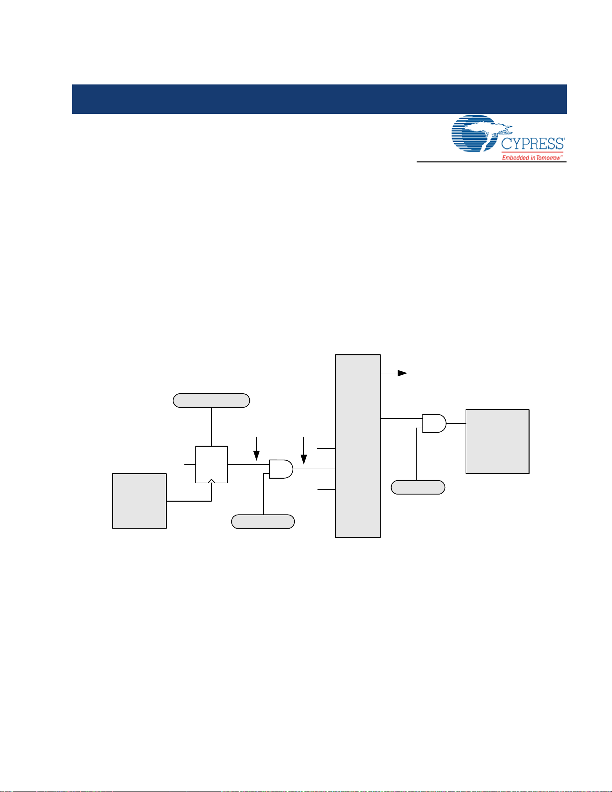
5. Interrupt Controller
M8C Core
Interrupt
Source
(Timer,
GPIO, etc.)
Interrupt Taken
or
Posted
Interrupt
Pending
Interrupt
GIE
Interrupt Vector
Mask Bit Setting
DRQ1
Priority
Encoder
Interrupt
Request
...
INT_MSKx:n
INT_CLRx:n Write
CPU_F[0]
...
n
0
This chapter presents the Interrupt Controller and its associated registers. The interrupt controller provides a mechanism for a
hardware resource in PSoC devices, to change program execution to a new address without regard to the current task being
performed by the code being executed. For a complete table of the Interrupt Controller registers, refer to the “Summary Table
of the Core Registers” on page 32. For a quick reference of all PSoC registers in address order, refer to the Register
Details chapter on page 47.
5.1 Architectural Description
A block diagram of the PSoC Interrupt Controller is shown in Figure 5-1, illustrating the concepts of posted interrupts and
pending interrupts.
Figure 5-1. Interrupt Controller Block Diagram
The sequence of events that occur during interrupt processing is as follows.
1. An interrupt becomes active, either because (a) the
interrupt condition occurs (for example, a timer expires),
(b) a previously posted interrupt is enabled through an
update of an interrupt mask register, or (c) an interrupt is
pending and GIE is set from ‘0’ to ‘1’ in the CPU Flag
register.
2. The current executing instruction finishes.
3. The internal interrupt routine executes, taking 13 cycles.
During this time, the following actions occur:
■ The PCH, PCL, and Flag register (CPU_F) are
pushed onto the stack (in that order).
Document # 001-20559 Rev. *D 61
■ The CPU_F register is then cleared. Since this clears
the GIE bit to 0, additional interrupts are temporarily
disabled.
■ The PCH (PC[15:8]) is cleared to zero.
■ The interrupt vector is read from the interrupt control-
ler and its value is placed into PCL (PC[7:0]). This
sets the program counter to point to the appropriate
address in the interrupt table (for example, 001Ch for
the GPIO interrupt).
4. Program execution vectors to the interrupt table. Typically, a LJMP instruction in the interrupt table sends execution to the user's interrupt service routine (ISR) for this
interrupt. (See “Instruction Set Summary” on page 36.)
Page 62

Interrupt Controller
5. The ISR executes. Note that interrupts are disabled
since GIE = 0. In the ISR, interrupts can be re-enabled if
desired, by setting GIE = 1 (take care to avoid stack
overflow in this case).
6. The ISR ends with a RETI instruction. This pops the Flag
register, PCL, and PCH from the stack, restoring those
registers. The restored Flag register re-enables interrupts, since GIE = 1 again.
7. Execution resumes at the next instruction, after the one
that occurred before the interrupt. However, if there are
more pending interrupts, the subsequent interrupts are
processed before the next normal program instruction.
Interrupt Latency. The time between the assertion of an
enabled interrupt and the start of its ISR can be calculated
using the following equation:
Latency = Equation 1
Time for current instruction to finish +
Time for M8C to change program counter to interrupt address +
Time for LJMP instruction in interrupt table to exe cute.
For example, if the 5-cycle JMP instruction executes when
an interrupt becomes active, the total number of CPU clock
cycles before the ISR begins is as follows:
(1 to 5 cycles for JMP to finish) + Equation 2
(13 cycles for interrupt routine) +
(7 cycles for LJMP) = 21 to 25 cycles.
In the example above, at 24 MHz, 25 clock cycles take
1.042 s.
5.1.1 Posted versus Pending Interrupts
An interrupt is posted when its interrupt conditions occur.
This results in the flip-flop in Figure 5-1 clocking in a ‘1’. The
interrupt remains posted until the interrupt is taken or until it
is cleared by writing to the appropriate INT_CLRx register.
A posted interrupt is not pending unless it is enabled by setting its interrupt mask bit (in the appropriate INT_MSKx register). All pending interrupts are processed by the priority
encoder to determine the highest priority interrupt to be
taken by the M8C if the Global Interrupt Enable bit is set in
the CPU_F register.
Disabling an interrupt by clearing its interrupt mask bit (in
the INT_MSKx register) does not clear a posted interrupt,
nor does it prevent an interrupt from being posted. It simply
prevents a posted interrupt from becoming pending.
It is especially important to understand the functionality of
clearing posted interrupts, if the configuration of the PSoC
device is changed by the application.
For example, if a digital PSoC block is configured as a counter and has posted an interrupt but is later reconfigured to a
serial communications receiver, the posted interrupt from
the counter remains. Therefore, if the digital PSoC block's
INT_MSKx bit is set after configuring the block as a serial
communications receiver, a pending interrupt is generated
immediately. To prevent the carryover of posted interrupts
from one configuration to the next, the INT_CLRx registers
should be used to clear posted interrupts prior to enabling
the digital PSoC block.
Interrupt Priority . The priorities of the interrupts only come
into consideration if more than one interrupt is pending during the same instruction cycle. In this case, the priority
encoder (see Figure 5-1) generates an interrupt vector for
the highest priority interrupt that is pending.
62 Document # 001-20559 Rev. *D
Page 63

Interrupt Controller
5.2 Application Description
The interrupt controller and its associated registers allow the user ’s code to respond to an in terrupt from almost every functional block in the PSoC devices. Interrupts for all the digital blocks and each of the analog columns are available, as well as
interrupts for supply voltage, sleep, variable clocks, and a general GPIO (pin) interrupt.
The registers associated with the interrupt controller allow interrupts to be disabled either globally or individually. The registers
also provide a mechanism by which a user can clear all pendin g and posted interrupts, or clear indivi dual posted or pe nding
interrupts. A software mechanism is provided to set individual interrupts. Setting an interrupt by way of software is very useful
during code development, when one may not have the complete hardware system necessary to generate a real interrupt.
The following table lists the interrupts for all PSoC devices (highlighting specifically the CY8C24533, CY8C23533,
CY8C23433CY8C24633) and the priorities that are available in each PSoC device.
Table 5-1. PSoC Device Interrupt Table
CY8C24633CY8
Interrupt Priority Interrupt Address
0 (Highest) 0000h
1 0004h
2 0008h
3000Ch
5 0014h
6 0018h
7001Ch
8 0020h
9 0024h
10 0028h
11 002Ch
24 0060h
25 (Lowest) 0064h
C24533,
CY8C23533,
CY8C23433
Interrupt Name
Reset
Supply Voltage Monitor
Analog Column 0
Analog Column 1
SAR8 ADC
VC3
GPIO
PSoC Block DBB00
PSoC Block DBB01
PSoC Block DCB02
PSoC Block DCB03
I2C
Sleep Timer
Document # 001-20559 Rev. *D 63
Page 64

Interrupt Controller
5.3 Register Definitions
The following registers are associated with the Interrupt Con troller and are listed in addre ss order. The register descriptions
have an associated register table showing the bit structure for that register. The bits in the tables that are grayed out are
reserved bits and are not detailed in the register descriptions that follow. Reserved bits should always be written with a value
of ‘0’. For a complete table of Interrupt Controller registers, refer to the “Summary Table of the Core Registers” on page 32.
Depending on the PSoC device you have, only certain bits are accessible to be read or written, such as the INT_CLR0 and
INT_MSK0 registers that are analog column and digital row dependent. The analog column dependent registers have the column number listed to the right of the Address column. The digital row dependent registers are set up the same way, only with
the term “Row” in the Address column.
5.3.1 INT_CLRx Registers
Address Name Bit 7 Bit 6 Bit 5 Bit 4 Bit 3 Bit 2 Bit 1 Bit 0 Access
0,DAh
0,DBh
0,DDh
INT_CL
R0
INT_CL
R1
INT_CL
R3
VC3 Sleep GPIO SAR8 ADC Analog 1 Analog 0 V Monitor RW : 0
DCB03 DCB02 DBB01 DBB00 RW : 0
I2C RW : 0
The Interrupt Clear Registers (INT_CLRx) are used to
enable the individual interrupt sources’ ability to clear posted
interrupts.
There are three interrupt clear registers (INT_CLR0,
INT_CLR1, and INT_CLR3) which may be referred to in
general as INT_CLRx.The INT_CLRx registers are similar to
the INT_MSKx registers in that they hold a bit for each interrupt source. Functionally the INT_CLRx registers are similar
to the INT_VC register, although their operation is completely independent. When an INT_CLRx register is read,
any bits that are set indicate an interrupt has been posted
for that hardware resource. Therefore, reading these registers gives the user the ability to determine all posted interrupts.
The Enable Software Interrupt (ENSWINT) bit in
INT_MSK3[7] determines the way an individual bit value
written to an INT_CLR0 register is interpreted. When
ENSWINT is cleared (the default state), writing 1's to an
INT_CLRx register has no effect. However, writing 0's to an
INT_CLRx register, when ENSWINT is cleared, causes the
corresponding interrupt to clear. If the ENSWINT bit is set,
any 0's written to the INT_CLRx registers are ignored. However, 1's written to an INT_CLRx register, while ENSWINT is
set, causes an interrupt to post for the corresp onding interrupt.
Note When using the INT_CLRx register to post an interrupt, the hardware interrupt source, such as a digital clock,
must not have its interrupt output high. Therefore, it may be
difficult to use software interrupts with interrupt sources that
do not have enables such as VC3.
Software interrupts can aid in debugging interrupt service
routines by eliminating the need to create system level inter-
actions that are sometimes necessary to create a hardwareonly interrupt.
5.3.1.1 INT_CLR0 Register
Bit 7: VC3. This bit allows posted VC3 interrupts to be
read, cleared, or set.
Bit 6: Sleep. This bit allows posted sleep interrupts to be
read, cleared, or set.
Bit 5: GPIO. This bit allows posted GPIO interrupts to be
read, cleared, or set.
Bit 4: SAR8 ADC. This bit allows posted SAR8 ADC interrupts to be read, cleared, or set.
Bit 3: Analog 2. This bit allows posted analog column 2
interrupts to be read, cleared, or set.
Bit 2: Analog 1. This bit allows posted analog column 1
interrupts to be read, cleared, or set.
Bit 1: Analog 0. This bit allows posted analog column 0
interrupts to be read, cleared, or set.
Bit 0: V Monitor. This bit allows posted V monitor interrupts to be read, cleared, or set.
For additional information, refer to the INT_CLR0 register on
page 99 .
64 Document # 001-20559 Rev. *D
Page 65

Interrupt Controller
5.3.1.2 INT_CLR1 Register
Bit 3: DCB03. This bit allows posted DCB03 interrupts to
be read, cleared, or set for row 0 block 3.
Bit 2: DCB02. This bit allows posted DCB02 interrupts to
be read, cleared, or set for row 0 block 2.
5.3.1.3 INT_CLR3 Register
Bit 0: I2C. This bit allows posted I2C interrupts to be read,
cleared, or set.
For additional information, refer to the INT_CLR3 register on
page 102.
Bit 1: DBB01. This bit allows posted DBB01 interrupts to
be read, cleared, or set for row 0 block 1.
Bit 0: DBB00. This bit allows posted DBB00 interrupts to
be read, cleared, or set for row 0 block 0.
For additional information, refer to the INT_CLR1 register on
page 101.
5.3.2 INT_MSKx Registers
Address Name Bit 7 Bit 6 Bit 5 Bit 4 Bit 3 Bit 2 Bit 1 Bit 0 Access
0,DEh
0,E0h
0,E1h
INT_MS
K3
INT_MS
K0
INT_MS
K1
ENSWINT I2C RW : 00
VC3 Sleep GPIO SAR8 ADC Analog 1 Analog 0 V Monitor RW : 00
DCB03 DCB02 DBB01 DBB00 RW : 00
The Interrupt Mask Registers (INT_MSKx) are used to
enable the individual interrupt sources’ ability to create
pending interrupts.
There are three interrupt mask registers (INT_MSK0,
INT_MSK1, and INT_MSK3) which may be referred to in
general as INT_MSKx. If cleared, each bit in an INT_MSKx
register prevents a posted interrupt from becoming a pending interrupt (input to the priority encoder). However, an
interrupt can still post even if its mask bit is zero. All
INT_MSKx bits are independent of all other INT_MSKx bits.
If an INT_MSKx bit is set, the interrupt source associated
with that mask bit may generate an interrupt that becomes a
pending interrupt. For example, if INT_MSK0[5] is set and at
least one GPIO pin is configured to generate an interrupt,
the interrupt controller allows a GPIO interrupt request to
post and become a pending interrupt for the M8C to respond
to. If a higher priority interrupt is generated before the M8C
responds to the GPIO interrupt, the higher priority interrupt
is responded to and not the GPIO interrupt.
Each interrupt source may require configuration at a block
level. Refer to the other chapters in this manual for information on how to configure an individual interrupt source.
5.3.2.1 INT_MSK3 Register
Bit 7: ENSWINT. This bit is a special non-mask bit that
controls the behavior of the INT_CLRx registers. See the
INT_CLRx register in this section for more information.
Bit 0: I2C. This bit allows posted I2C interrupts to be read,
masked, or set.
For additional information, refer to the INT_MSK3 register
on page 103.
Document # 001-20559 Rev. *D 65
Page 66

Interrupt Controller
5.3.2.2 INT_MSK0 Register
Bit 7: VC3. This bit allows posted VC3 interrupts to be
read, masked, or set.
Bit 6: Sleep. This bit allows posted sleep interrupts to be
read, masked, or set.
Bit 5: GPIO. This bit allows posted GPIO interrupts to be
read, masked, or set.
Bit 4: SAR8 ADC. This bit allows posted SAR8 ADC interrupts to be read, masked, or set.
Bit 3: Analog 2. This bit allows posted analog column 2
interrupts to be read, masked, or set.
Bit 2: Analog 1. This bit allows posted analog column 1
interrupts to be read, masked, or set.
Bit 1: Analog 0. This bit allows posted analog column 0
interrupts to be read, masked, or set.
Bit 0: V Monitor. This bit allows posted V monitor interrupts to be read, masked, or set.
For additional information, refer to the INT_MSK0 register
on page 104.
5.3.2.3 INT_MSK1 Register
Bit 3: DCB03. This bit allows posted DCB03 interrupts to
be read, masked, or set for row 0 block 3.
Bit 2: DCB02. This bit allows posted DCB02 interrupts to
be read, masked, or set for row 0 block 2.
Bit 1: DBB01. This bit allows posted DBB01 interrupts to
be read, masked, or set for row 0 block 1.
Bit 0: DBB00. This bit allows posted DBB00 interrupts to
be read, masked, or set for row 0 block 0.
For additional information, refer to the INT_MSK1 register
on page 105.
5.3.3 INT_VC Register
Address Name Bit 7 Bit 6 Bit 5 Bit 4 Bit 3 Bit 2 Bit 1 Bit 0 Access
0,E2h
LEGEND
C Clearable register or bits.
INT_VC
The Interrupt Vector Clear Register (INT_VC) returns the
next pending interrupt and clears all pending interrupts
when written.
Bits 7 to 0: Pending Interrupt[7:0]. When the register is
read, the least significant byte (LSB), of the highest priority pending interrupt, is returned. For example, if the GPIO
and I2C interrupts are pending and the INT_VC register was
read, the value 1Ch is be read. However, if no interrupts are
pending, the value 00h is returned. This is the reset vector in
the interrupt table; however, reading 00h from the INT_VC
register should not be considered an indication that a system reset is pending. Rather, reading 00h from the INT_VC
register simply indicates that there are no pending interrupts.
Pending Interrupt[7:0] RC : 00
The highest priority interrupt, indicated by the value returned
by a read of the INT_VC register, is removed from the list of
pending interrupts when the M8C services an interrupt.
Reading the INT_VC register has limited usefulness. If interrupts are enabled, a read to the INT_VC register does not
determine that an interrupt was pending before the interrupt
was actually taken. However, while in an interrupt, a user
may wish to read the INT_VC register to see what the next
interrupt is. When the INT_VC register is written, with any
value, all pending and posted interrupts are cleared by
asserting the clear line for each interrupt.
For additional information, refer to the INT_VC register on
page 106.
66 Document # 001-20559 Rev. *D
Page 67

Interrupt Controller
5.3.4 CPU_F Register
Address Name Bit 7 Bit 6 Bit 5 Bit 4 Bit 3 Bit 2 Bit 1 Bit 0 Access
x,F7h
LEGEND
L The AND F, expr; OR F, expr; and XOR F, expr f l ag instructions can be used to modify this register.
x An “x” before the comma in the address field indicates that this register can be read or written to no matter what bank is used.
CPU_F
PgMode[1:0] XIO Carry Zero GIE RL : 02
The M8C Flag Register (CPU_F) provides read access to
the M8C flags. Note that only the GIE (Global Interrupt
Enable) bit is related to the interrupt controller.
Bits 7 to 1. The CPU_F register holds bits that are used by
different resources. For information on the other bits in this
register, refer to the CPU Core (M8C) chapter on page 35.
Bit 0: GIE. The state of the Global Interrupt Enable bit
determines whether interrupts (by way of the IRQ) are recognized by the M8C. This bit is set or cleared by the user,
using the flag-logic instructions (for example, OR F, 1).
GIE is also cleared automatically by the M8C upon entering
the interrupt service routine (ISR), after the flag byte has
been stored on the stack, preventing nested interrupts. Note
that the bit can be set in an ISR if desired.
For GIE=1, the M8C samples the IRQ input for each instruction. For GIE=0, the M8C ignores the IRQ.
For additional information, refer to the CPU_F register on
page 120.
Document # 001-20559 Rev. *D 67
Page 68

Interrupt Controller
68 Document # 001-20559 Rev. *D
Page 69

6. General Purpose IO (GPIO)
This chapter discusses the General Purpose IO (GPIO) and its associated registers, which is the circuit respon sible for interfacing to the IO pins of a PSoC device. The GPIO blocks provide the interface between the M8C core and the outside world.
They offer a large number of configurations to support several types of input/output (IO) operations for both digital and analog systems. For a complete table of the GPIO registers, refer to the “Summary Tab le of the Core Regi sters” on page 32. For
a quick reference of all PSoC registers in address order, refer to the Register Details chapter on page 47.
6.1 Architectural Description
The GPIO contains input buffers, output drivers, register bit
storage, and configuration logic for connecting the PSoC
device to the outside world.
IO ports are arranged with (up to) 8 bits per port. Each full
port contains eight identical GPIO blocks, with connections
to identify a unique address and register bit number for each
block. Each GPIO block can be used for the following types
of IO:
■ Digital IO (digital input and output controlled by software)
■ Global IO (digital PSoC block input and output)
■ Analog IO (analog PSoC block input and output)
Each IO pin also has several drive modes, as well as interrupt capabilities. While all GPIO pins are identical and provide digital IO, some pins may not connect internally to
analog functions.
The main block diagram for the GPIO block is shown in
Figure 6-1. Note that some pins do not have all of the func-
tionality shown, depending on internal connections.
6.1.1 Digital IO
One of the basic operations of the GPIO ports is to allow the
M8C to send information out of the PSoC device a nd get
information into the M8C from outside the PSoC device.
This is accomplished by way of the port data register
(PRTxDR). Writes from the M8C to the PRTxDR register
store the data state, one bit per GPIO. In the standard nonbypass mode, the pin drivers drive the pin in response to
this data bit, with a drive strength determined by the Drive
mode setting (see Figure 6-1). The actual voltage on the pin
depends on the Drive mode and the external load.
Note that the pin voltage can represent a different logic
value than the last value written to the PRTxDR register.
This is an important distinction to remember in situations
such as the use of a read modify write to a PRTxDR register.
Examples of read modify write instructions include AND,
OR, and XOR.
The following is an example of how a read modify write, to a
PRTxDR register, can have an unexpected and even indeterminate result in certain systems. Consider a scenario
where all bits of Port 1 on the PSoC device are in the Strong
1 Resistive 0 Drive mode; so that in some cases, the system
the PSoC is in may pull up one of the bits.
mov reg[PRT1DR], 0x00
or reg[PRT1DR], 0x80
In the first line of code above, writing a 0x00 to the port does
not affect any bits that happen to be driven by the system
the PSoC is in. However, in the second line of code, it does
not guarantee that only bit 7 is the one se t to a strong 1.
Because the OR instruction first reads the port, any bits that
are in the pull up state are read as a ‘1’. These ones are
then written back to the port. When this happens, the pin
goes into a strong 1 state; therefore, if the pull up condition
ends in the system, the PSoC keeps the pin value at a logic
1.
The M8C can read the value of a port by reading the
PRTxDR register address. When the M8C reads the
PRTxDR register address, the current value of the pin voltage is translated into a logic value and returned to the M8C.
Document # 001-20559 Rev. *D 5
Page 70

General Purpose IO (GPIO)
DM[2:0]=110b
R
DENQ
RESET
I2C Input
Global
Input Bus
QinLatch
5.6K
Vdd
Write PRTxDR
2:1
Drive
Logic
DM2
DM1
DM0
DATA
2:1
BYP
Global
Output Bus
I2C Output
I2C Enable
Slew
Control
Vdd
5.6K
PIN
(To Readmux,
Interrupt Logic)
Output Path
Input Path
DM1
DM0
BYP
CELLRD
AIN
Data Bus
Read PRTxDR
INBUF
Vdd
0. 2. 3.
4. 5. 6. 7.
Drive Modes
DM1DM2
Drive Mode
0 0 0 Resistive Pull Down0ResistiveStron g
DM0
0 0 1 Strong Drive1St ro n gS tro ng
0 1 0 High Impedance 2 High Z High Z
0 1 1 Resistive Pull Up 3 Stro n gResistive
1 0 0 Open Drain, Drives H ig h 4 High ZStrong (Slow)
1 0 1 Slow Strong D rive 5Strong (Slow)Stron g (Slow)
1 1 0 High Impedance Analog6High ZHigh Z
1 1 1 Open Drain, Drives L ow7Strong (Slow)H igh Z
Diagram
Number
Data = 0 Data = 1
AOUT
1.
6.1.2 Global IO
The GPIO ports are also used to interconnect signals to and
from the digital PSoC blocks, as global inputs or outputs.
The global IO feature of each GPIO (port pin) is off by
default. To access the feature, two parameters must be
changed. To configure a GPIO as a global input, the port
global select bit must be set for the desired GPIO using the
PRTxGS register. This sets BYP = 1 in Figure 6-1 and disconnects the output of the PRTxDR register from the pin.
Also, the Drive mode for the GPIO must be set to the digital
High Z state. (Refer to the “PRTxDMx Registers” on page10
for more information.) To configure a GPIO as a global output, the port global select bit must again be set. But in this
case, the drive state must be set to any of the non-High Z
states.
Figure 6-1. GPIO Block Diagram
6.1.3 Analog Input
Analog signals can pass into the PSoC device core from
PSoC device pins through the block’s AOUT pin. This provides a resistive path (~300 ohms) directly through the
GPIO block. For analog modes, the GPIO block is typically
configured into a high impedance analog drive mode (High
Z). The mode turns off the Schmitt trigger on the input path,
which may reduce power consumption and decrease internal switching noise when using a particular IO as an analog
input. Refer to the Electrical Specifications chapter in the
device data sheet.
6 Document # 001-20559 Rev. *D
Page 71

General Purpose IO (GPIO)
Low
PRTxIE:n
High
Change
DQ
S
R
INTO
INBUF (from figure 1 in ch apter)
CELLRD
EN
QinLatch
Interrupt Mode
PRTxIC0:n
PRTxIC1:n
Output
0 0 Disabled
0 1 Low
1 0 High
1 1 Change from last read
Vss
PRTxIC1:n
PRTxIC0:n
PRTxIC1:n
PRTxIC0:n
PRTxIC1:n
PRTxIC0:n
6.1.4 GPIO Block Interrupts
Each GPIO block can be individually configured for interrupt
capability. Blocks are configured by pin interrupt enables
and also by selection of the interrupt state. Blocks can be
set to interrupt when the pin is high, low, or when it changes
from the last time it was read. The block provides an opendrain interrupt output (INTO) that is connected to other
GPIO blocks in a wire-OR fashion.
All pin interrupts that are wire-OR’ed together are tied to the
same system GPIO interrupt. Therefore, if interrupts are
enabled on multiple pins, the user’s interrupt service routine
must provide a mechanism to determine which pin was the
source of the interrupt.
Using a GPIO interrupt requires the following steps:
1. Set the Interrupt mode in the GPIO pin block.
2. Enable the bit interrupt in the GPIO block.
3. Set the mask bit for the (global) GPIO interrupt.
4. Assert the overall Global Interrupt Enable.
The first two steps, bit interrupt enable and Interrupt mode,
are set at the GPIO block level (that is, at each port pin), by
way of the block’s configuration registers.
The last two steps are common to all interrupts and are
described in the Interrupt Controller chapter on page 61.
At the GPIO block level, asserting the INTO line depends
only on the bit interrupt enable and the state of the pin relative to the chosen Interrupt mode. At the PSoC device level,
due to their wire-OR nature, the GPIO interrupts are neither
true edge-sensitive interrupts nor true level-sensitive interrupts. They are considered edge-sensitive for asserting, but
level-sensitive for release of the wire-OR interrupt line.
pin transitions, if not already transitioned, appropriately high
or low, to match the Interrupt mode configuration. Once this
happens, the INTO line pulls low to assert the GPIO interrupt. This assumes the other system-level enables are on,
such as setting the global GPIO interrupt enable and the
Global Interrupt Enable. Setting the pin interrupt enable may
immediately assert INTO, if the Interrupt mode conditions
are already being met at the pin.
Once INTO pulls low, it continues to hold INTO low until one
of these conditions change: (a) the pin interrupt enable is
cleared; (b) the voltage at pin transitions to the opposite
state; (c) in interrupt-on-change mode, the GPIO data register is read, thus setting the local interrupt level to the opposite state; or (d) the Interrupt mode is changed so that the
current pin state does not create an interrupt. Once one of
these conditions is met, the INTO releases. At this point,
another GPIO pin (or this pin again) could assert its INTO
pin, pulling the common line low to assert a new interrupt.
Note that the GPIO data register state is latched during read
operation. Interrupt-on-change may not behave as expected
if the input signal changes during the metastability time of
the latch, that is, when the GPIO is being read.
Note the following behavior from this level-release feature. If
one pin is asserting INTO and then a second pin asserts its
INTO, when the first pin releases its INTO, the second pin is
already driving INTO and thus no change is seen (that is, no
new interrupt is asserted on the GPIO interrupt). Care must
be taken, using polling or the states of the GPIO pin and
Global Interrupt Enables, to catch all interrupts among a set
of wire-OR GPIO blocks.
Figure 6-2 shows the interrupt logic portion of the block.
If no GPIO interrupts are asserting, a GPIO interrupt occurs
whenever a GPIO pin interrupt enable is set and the GPIO
Document # 001-20559 Rev. *D 7
Figure 6-2. GPIO Interrupt Logic Diagram
Page 72

General Purpose IO (GPIO)
6.2 Register Definitions
The following registers are associated with the General Purpose IO (GPIO) and are liste d in address order. The register
descriptions in this section have an associated register table showing the bit structure for that register. For a complete table of
GPIO registers, refer to the “Summary Table of the Core Registers” on page 32.
For a selected GPIO block, the individual registers are addressed in the Summary Table of the Core Registers. In the register
names, the ‘x’ is the port number, configured at the PSoC device level (x = 0 to 7, typically). All register values are readable,
except for the PRTxDR register; reads of this register return the pin state instead of the register bit state.
6.2.1 PRTxDR Registers
Address Name Bit 7 Bit 6 Bit 5 Bit 4 Bit 3 Bit 2 Bit 1 Bit 0 Access
0,xxh
LEGEND
xx An “x” after the comma in the address field indicates that there are multiple instances of the register. For an exp anded address listing of these registers,
refer to the
PRTxDR
“Summary Table of the Core Registers” on page 32.
Data[7:0] RW : 00
The Port Data Register (PRTxDR) allows for write or read
access of the current logical equivalent of the voltage on the
pin.
Reading the PRTxDR register returns the actual pin state,
as seen by the input buffer. This may not be the same as the
expected output state, if the load pulls the pin more strongly
than the pin’s configured output drive. See “Digital IO” on
Bits 7 to 0: Data[7:0]. Writing the PRTxDR register bits
sets the output drive state for the pin to high (for DIN=1) or
low (DIN=0), unless a bypass mode is selected (either I2C
Enable=1, or the global select register written high).
page 5 for a detailed discussion of digital IO.
For additional information, refer to the PRTxDR register on
page 49 .
6.2.2 PRTxIE Registers
Address Name Bit 7 Bit 6 Bit 5 Bit 4 Bit 3 Bit 2 Bit 1 Bit 0 Access
0,xxh
LEGEND
xx An “x” after the comma in the address field indicates that there are multiple instances of the register. For an exp anded address listing of these registers,
refer to the
PRTxIE
“Summary Table of the Core Registers” on page 32.
The Port Interrupt Enable Register (PRTxIE) is used to
enable/disable the interrupt enable internal to the GPIO
block.
Interrupt Enables[7:0] RW : 00
Bits 7 to 0: Interrupt Enables[7:0]. A ‘1’ enables the INTO
output at the block and a ‘0’ disable s INTO so it is on ly Hi gh
Z.
For additional information, refer to the PRTxIE register on
page 50 .
8 Document # 001-20559 Rev. *D
Page 73

General Purpose IO (GPIO)
6.2.3 PRTxGS Registers
Address Name Bit 7 Bit 6 Bit 5 Bit 4 Bit 3 Bit 2 Bit 1 Bit 0 Access
0,xxh
LEGEND
xx An “x” after the comma in the address field indicates that there are multiple instances of the register. For an expanded address listing of these registers,
refer to the
PRTxGS
“Summary Table of the Core Registers” on page 32.
Global Select[7:0] RW : 00
The Port Global Select Register (PRTxGS) is used to select
the block for connection to global inputs or outputs.
Bits 7 to 0:Global Select[7:0]. Writing this register high
enables the global bypass (BYP = 1 in Figure 6-1). If the
Drive mode is set to digital High Z (DM[2:0] = 010b), then
the pin is selected for global input (PIN drives to the Global
Input Bus). In non-High Z modes, the block is selected for
global output (the Global Output Bus drives to PIN), bypassing the data register value (assuming I2C Enable = 0).
If the PRTxGS register is written to zero, the global in/out
function is disabled for the pin and the pin reflects the value
of PRT_DR.
For additional information, refer to PRTxGS register on page
51.
Document # 001-20559 Rev. *D 9
Page 74

General Purpose IO (GPIO)
6.2.4 PRTxDMx Registers
Address Name Bit 7 Bit 6 Bit 5 Bit 4 Bit 3 Bit 2 Bit 1 Bit 0 Access
0,xxh
PRTxDM
2
1,xxh
PRTxDM
0
1,xxh
PRTxDM
1
LEGEND
xx An “x” after the comma in the address field indicates that there are multiple instances of the register. For an expanded address listing of these registers,
refer to the
“Summary Table of the Core Registers” on page 32.
Drive Mode 2[7:0] RW : FF
Drive Mode 0[7:0] RW : 00
Drive Mode 1[7:0] RW : FF
The Port Drive Mode Bit Registers (PRTxDMx) are used to
specify the Drive mode for GPIO pins.
Bits 7 to 0: Drive Mode x[7:0]. In the PRTxDMx registers
there are eight possible drive modes for each port pin. Three
mode bits are required to select one of these modes, and
these three bits are spread into three different registers
(PRTxDM0, PRTxDM1, and PRTxDM2). The bit position of
the effected port pin (for example, Pin[2] in Port 0) is the
same as the bit position of each of the three drive mode register bits that control the Drive mode for that pin (for example, bit[2] in PRT0DM0, bit[2] in PRT0DM1, and bit[2] in
PRT0DM2). The three bits from the three registers are
treated as a group. These are referred to as DM2, DM1, and
DM0, or together as DM[2:0]. Drive modes are shown in
Table 6-1.
For analog IO, the Drive mode should be set to one of the
High Z modes, either 010b or 110b. The 110b mode has the
advantage that the block’s digital input buffer is disabled, so
no crowbar current flows even when the analog input is not
close to either power rail. When digital inputs are needed on
the same pin as analog inputs, the 010b Drive mode should
be used. If the 110b Drive mode is used, the pin is always
read as a zero by the CPU and the pin is not able to generate a useful interrupt. (It is not strictly required that a High Z
mode be selected for analog operation.)
For global input modes, Drive mode must be set to 010b.
Table 6-1. Pin Drive Modes
Drive Modes
DM2 DM1 DM0
0 0 0 Resistive pull down Strong high, resistive low
0 0 1 Strong drive Strong high, strong low
0 1 0 High impedance High Z high and low, digital
0 1 1 Resistive pull up Resistive high, strong low
1 0 0 Open drain high Slow strong high, High Z low
1 0 1 Slow strong drive Slow strong high, slow strong
1 1 0 High impedance,
1 1 1 Open drain low Slow strong low, High Z high
Pin State Description
input enabled
low
analog (reset state)
High Z high and low, digital
input disabled (for zero
power) (reset state)
The GPIO provides a default Drive mode of high imped-
ance, analog (High Z). This is achieved by forcing the reset
state of all PRTxDM1 and PRTxDM2 registers to FFh.
The resistive drive modes place a resistance in series with
the output, for low outputs (mode 000b) or high outputs
(mode 011b). Strong Drive mode 001b gives the fastest
edges at high DC drive strength. Mode 101b gives the same
drive strength but with slower edges. The open-drain modes
(100b and 111b) also use the sl ower edge rate drive. These
modes enable open-drain functions such as I2C mode 111b
(although the slow edge rate is not slow enough to meet the
I2C fast mode specification).
For additional information, refer to the PRTxDM2 register on
page 52, the PRTxDM0 register on page 123, and the
PRTxDM1 register on page 124.
10 Document # 001-20559 Rev. *D
Page 75

General Purpose IO (GPIO)
Last Value Read From Pin was ‘0’
Pin State Waveform
GPIO pin
interrupt
enable set
Interrupt
occurs
(a)
Pin State Waveform
GPIO pin
interrupt
enable set
Interrupt
occurs
(b)
Last Value Read From Pin was ‘1’
Pin State Waveform
GPIO pin
interrupt
enable set
Interrupt
occurs
(c)
Pin State Waveform
GPIO pin
interrupt
enable set
Interrupt
occurs
(d)
6.2.5 PRTxICx Registers
Address Name Bit 7 Bit 6 Bit 5 Bit 4 Bit 3 Bit 2 Bit 1 Bit 0 Access
1,xxh
1,xxh
LEGEND
xx An “x” after the comma in the address field indicates that there are multiple instances of the register. For an expanded address listing of these registers,
refer to the
PRTxIC0
PRTxIC1
“Summary Table of the Core Registers” on page 32.
Interrupt Control 0[7:0] RW : 00
Interrupt Control 1[7:0] RW : 00
The Port Interrupt Control Registers (PRTxIC1 and
PRTxIC0) are used to specify the Interrupt mode for GPIO
pins.
Bits 7 to 0: Interrupt Control x[7:0]. In the PRTxICx registers, the Interrupt mode for the pin is determined by bi ts in
these two registers. These are referred to as IC1 and IC0, or
together as IC[1:0].
There are four possible interrupt modes for each port pin.
Two mode bits are required to select one of these modes
and these two bits are spread into two different registers
(PRTxIC0 and PRTxIC1). The bit position of the effected
port pin (for example, Pin[2] in Port 0) is the same as the bit
position of each of the interrupt control register bits that control the Interrupt mode for that pin (for example, bit[2] in
PRT0IC0 and bit[2] in PRT0IC1). The two bits from the two
registers are treated as a group.
The Interrupt mode must be set to one of the non-zero
modes listed in Table 6-2, in ord er to get an interrupt from
the pin.
The GPIO Interrupt mode “disabled” (00b) disables interrupts from the pin, even if the GPIO’s bit interrupt enable is
on (from the PRTxIE register).
Interrupt mode 01b means that the block asserts the interrupt line (INTO) when the pin voltage is low, providing the
block’s bit interrupt enable line is set (high).
Interrupt mode 10b means that the block asserts the interrupt line (INTO) when the pin voltage is high, providing the
block’s bit interrupt enable line is set (high).
Interrupt mode 11b means that the block asserts the interrupt line (INTO) when the pin voltage is the opposite of the
last state read from the pin, providing the block’s bit interrupt
enable line is set high. This mode switches between low
mode and high mode, depending on the last value read from
the port during reads of the data register (PRTxDR). If the
last value read from the GPIO was ‘0’, the GPIO subsequently is in Interrupt High mode.
If the last value read from the GPIO was ‘1’, the GPIO then
is in Interrupt Low mode.
Table 6-2. GPIO Interrupt Modes
Interrupt Modes
IC1 IC0
0 0 Bit interrupt disabled, INTO de-asserted
0 1 Assert INTO when PIN = low
1 0 Assert INTO when PIN = high
1 1 Assert INTO when PIN = change from last read
Description
Figure 6-3. GPIO Interrupt Mode 11b
Figure 6-3 assumes that the GIE is set, GPIO interrupt mask
is set, and that the GPIO Interrupt mode is set to 11b. The
Change Interrupt mode is different from the other modes, in
that it relies on the value of the GPIO’s read latch to determine if the pin state has changed. Therefore, the port that
contains the GPIO in question must be read during every
interrupt service routine. If the port is not read, the Interrupt
mode acts as if it is in high mode when the latch value is ‘0’
and low mode when the latch value is ‘1’.
For additional information, refer to the PRTxIC0 register on
page 125 and the PRTxIC1 register on page 126.
Document # 001-20559 Rev. *D 11
Page 76

General Purpose IO (GPIO)
12 Document # 001-20559 Rev. *D
Page 77

7. Analog Output Drivers
P0[5]
P0[3]
P0[4]
P0[2]
Analog
Array
ACB01
ASD11
ASC21
ACB00
SAR8
ADC
ACB02
ASC12
ASD22
ACB03
ASD13
ASC23
Analog
Output
Drivers
This chapter presents the Analog Output Drivers and their associated register. The analog output drivers provide a means for
driving analog signals off the PSoC device. For a quick reference of all PSoC registers in address order, refer to the Register
Details chapter on page 47. For information on the analog system, refer to the “Analog System” on page 215.
7.1 Architectural Description
The CY8C24533, CY8C23533, CY8C23433CY8C24633
PSoC devices have up to two analog drivers used to output
analog values on port pins.
Table 7-1. PSoC Analog Output Drivers
Port Pin
CY8C23533
CY8C23433
P0[5]
P0[4]
P0[3]
P0[2]
CY8C24x23A
CY8C24533CY8C24633
Figure 7-1. Analog Output Drivers for CY8C24533, CY8C23533, CY8C23433CY8C24633
Each of these drivers is a resource available to all the ana-
log blocks in a particular analog column. Therefore, the
number of analog output drivers matches the number of
analog columns in a device. The user must select no more
than one analog block per column to drive a signal on its
analog output bus (ABUS), to serve as the i nput to the analog driver for that column. The output from the analog output
driver for each column can be enabled and disabled using
the Analog Output Driver register ABF_CR0. If the analog
output driver is enabled, then it must have an analog block
driving the ABUS for that column. Otherwise, the analog
output driver can enter a high current consumption mode.
Figure 7-1 illustrates the drivers and their relationship within
the analog array. For a detailed drawing of the analog output
drivers in relation to the analog system, refer to the Analog
Input Configuration chapter on page 241.
Document # 001-20559 Rev. *D 13
Page 78

Analog Output Drivers
7.2 Register Definitions
The following register is associated with the Ana log Outpu t Dr ivers. The regi ster description has an associated register table
showing the bit structure of the register. The bits that are grayed out in the table below are rese rve d bi ts and are no t detail ed
in the register description that follows. Reserved bits should always be written with a value of ‘0’. Depending on the number of
analog columns your PSoC device has (see the Cols. column in the register table below), some bits may be reserved (refer to
the table titled “PSoC Device Characteristics” on page 20).
7.2.1 ABF_CR0 Register
Add. Name Bit 7 Bit 6 Bit 5 Bit 4 Bit 3 Bit 2 Bit 1 Bit 0 Access
1,62h
ABF_CR0
ACol1Mux ABUF1EN ABUF0EN Bypass PWR RW : 00
The Analog Output Buffer Control Register 0 (ABF_CR0)
controls analog input muxes from Port 0 and the output buffer amplifiers that drive column outputs to device pins.
For more information on bit 7, see the Analog Input
Configuration chapter on page 241.
Bit 7: ACol1MUX. A mux selects the output of column 0
input mux or column 1 input mux. When set, this bit sets the
column 1 input to column 0 input mux output.
Bit 5: ABUF1EN. Enables the analog output buffer for Analog Column 1 (Pin P0[5]). A ‘0’ disables the analog output
buffer, a ‘1’ enables.
Bit 3: ABUF0EN. Enables the analog output buffer for Ana-
log Column 0 (Pin P0[3]). (1 Column: AGND). A ‘0’ disables
the analog output buffer, a ‘1’ enables
Bit 1: Bypass. Bypass mode connects the analog output
driver input directly to the output. When this bit is set, all
analog output drivers are in bypass mode. This is a high
impedance connection used primarily for measurement a nd
calibration of internal references. Use of this feature is not
recommended for customer designs.
Bit 0: PWR. This bit is used to set the power level of the
analog output drivers. When this bit is set, all of the a nalog
output drivers are in a High Power mode.
For additional information, refer to the ABF_CR0 register on
page 135.
14 Document # 001-20559 Rev. *D
Page 79

8. Internal Main Oscillator (IMO)
This chapter presents the Internal Main Oscillator (IMO) and its associated registers. Th e IMO produces clock signals of 24
MHz and 48 MHz. For a complete table of the IMO registers, refer to the “Summary Table of the Core Registers” on page 32.
For a quick reference of all PSoC registers in address order, refer to the Register Details chapter on page 47.
8.1 Architectural Description
The Internal Main Oscillator (IMO) outputs two clocks: a
SYSCLK, which can be the internal 24 MHz clock or an
external clock, and a SYSCLKX2 that is always twice the
SYSCLK frequency. In the absence of a high-precision input
source from the 32.768 kHz crystal oscillator, the accuracy
of the internal 24/48 MHz clocks is ±2.5% over temperature
variation and two voltage ranges (3.3V ± 0.3V and 5.0V ±
0.25%). No external components are required to achieve
this level of accuracy.
There is an option to phase lock this oscillator to the External Crystal Oscillator (ECO). The choice of crystal and its
inherent accuracy determines the overall accuracy of the
oscillator. The ECO must be stable prior to locking the frequency of the IMO to this reference source.
The frequency doubler circuit, which produces SYSCLKX2,
can be disabled to save power. The lower frequency SYSCLK settings are available by setting the slow IMO (SLIMO)
bit in the CPU_SCR1 register. With this bit set and the corresponding factory trim value applied to the IMO_TR register,
SYSCLK can be lowered to 6 MHz. This offers lower device
power consumption for systems that can operate with the
reduced system clock. Slow IMO mode is discussed further
in the “Application Description” on page 15.
8.2 Application Description
To save power, the IMO frequency can be reduced from 24
MHz to 6 MHz or 12 MHz using the SLIMO bit in the
CPU_SCR1 register, in conjunction with the Trim values in
the IMO_TR register. Note that the CY8C27x43,
CY8C24533, CY8C23533, CY8C23433, CY8C24633,
CY8C24x23, CY8C22x13, CY7C603xx, and CYWUSB6953
devices do not have this functionality.
8.2.1 Trimming the IMO
An 8-bit register (IMO_TR) is used to trim the IMO. Bit 0 is
the LSB and bit 7 is the MSB. The trim step size is approximately 80 kHz.
A factory trim setting is loaded into the IMO_TR register at
boot time for 5V ± 0.25V operation, except for the
CY7C603xx, which is 3.3V ± 0.25V . For operation in the voltage ranges of 3.3V ± 0.3V and 2.7V ± 0.3V, user code must
modify the contents of this register with values stored in
Flash bank 0 as shown in Table 3-11 on page 49. This is
done with a Table Read command to the Supervisory ROM.
Document # 001-20559 Rev. *D 15
Page 80

Internal Main Oscillator (IMO)
8.3 Register Definitions
The following registers are associated with the Internal Mai n Oscillator (IMO). The register descriptions have an associated
register table showing the bit structure for that register. The bits in the tables that are grayed out are reserved bits and are not
detailed in the register descriptions that follow. Reserved bits should always be written with a value of ‘0’. For a complete table
showing all oscillator registers, refer to the “Summary Table of the Core Registers” on page 32.
8.3.1 CPU_SCR1 Register
Address Name Bit 7 Bit 6 Bit 5 Bit 4 Bit 3 Bit 2 Bit 1 Bit 0 Access
x,FEh
CPU_SC
R1
LEGEND
x An “x” before the comma in the address field indicates that this register can be read or written to no matter what bank is used.
# Access is bit specific. Refer to the
* Bits 3 and 2 (ECO EXW and ECO EX, respectively) cannot be used by the CY8C27x43 for silicon revision A, and by the CY8C24533, CY8C23533,
CY8C23433, CY8C24633, CY8C24x23, and CY8C22x13 PSoC devices.
IRESS SLIMO ECO EXW * ECO EX * IRAMDIS # : 00
Register Details chapter on page 47 for additional information.
The System Status and Control Register 1 (CPU_SCR1) is
used to convey the status and control of events related to
internal resets and watchdog reset.
Bit 7: IRESS. The Internal Reset Status bit is a read only bit
that may be used to determine if the booting process
occurred more than once.
When this bit is set, it indicates that the SROM SWBootReset code was executed more than once. If this bit is not set,
the SWBootReset executed only once. In either case, the
SWBootReset code does not allow execution from code
stored in Flash until the M8C Core is in a safe operating
mode with respect to supply voltage and Flash operation.
There is no need for concern when this bit is set. It is provided for systems which may be sensitive to boot time, so
that they can determine if the normal one-pass boot time is
exceeded. For more information on the SWBootReest code
see the Supervisory ROM (SROM) chapter on page 45.
Bit 4: SLIMO. When set, the Slow IMO bit allows the active
power dissipation of the PSoC device to be reduced by
slowing down the IMO from 24 MHz to 6 MHz. The IMO trim
value must also be changed when SLIMO is set. When not
in external clocking mode, the IMO is the source for SYSCLK; therefore, when the speed of the IMO changes, so
does SYSCLK.
Bit 3: ECO EXW. The ECO Exists Written bit is used as a
status bit to indicate that the ECO EX bit has been previ-
ously written to. It is read only. When this bit is a ‘1’, this indi-
cates that the CPU_SCR1 register has been written to and
is now locked. When this bit is a ‘0’, the register has not
been written to since the last reset event. Note that this bit
cannot be used by the CY8C27x43 for silicon revision A,
and by the CY8C24533, CY8C23533, CY8C23433,
CY8C24633, CY8C24x23, and CY8C22x13 PSoC devices.
Bit 2: ECO EX. The ECO Exists bit serves as a flag to the
hardware, to indicate that an external crystal oscillator
exists in the system. Just after boot, it may be written only
once to a value of ‘1’ (crystal exists) or ‘0’ (crystal does not
exist). If the bit is ‘0’, a switch-over to the ECO is locked out
by hardware. If the bit is ‘1’, hardware allows the firmware to
freely switch between the ECO and ILO. It should be written
as early as possible after a Power On Reset (POR) or
External Reset (XRES) event, where it is assumed that pro-
gram execution integrity is high. Note that this bit cannot be
used by the CY8C27x43 for silicon revision A, and by the
CY8C24533, CY8C23533, CY8C23433, CY8C24633,
CY8C24x23, and CY8C22x13 PSoC device s.
Bit 0: IRAMDIS. The Initialize RAM Disable bit is a control
bit that is readable and writeable. The defa ult valu e for this
bit is ‘0’, which indicates that the maximum amount of SRAM
should be initialized on watchdog reset to a value of 00h.
When the bit is ‘1’, the minimum amount of SRAM is initial-
ized after a watchdog reset. For more information on this bit,
see the “SROM Function Descriptions” on page 46.
For additional information, refer to the CPU_SCR1 register
on page 121.
16 Document # 001-20559 Rev. *D
Page 81

Internal Main Oscillator (IMO)
8.3.2 OSC_CR2 Register
Address Name Bit 7 Bit 6 Bit 5 Bit 4 Bit 3 Bit 2 Bit 1 Bit 0 Access
1,E2h
OSC_CR
2
PLLGAIN EXTCLKEN RSVD SYSCLKX2DIS RW : 00
The Oscillator Control Register 2 (OSC_CR2) is used to
configure various features of internal clock sources and
clock nets.
Bit 7: PLLGAIN. This is the only bit in the OSC_CR2 register that directly influences the PLL. When set, thi s bit keeps
the PLL in Low Gain mode. If this bit is held low, the lock
time is less than 10 ms. If this bit is held high, the lock time
is on the order of 50 ms. After lock is achieved, it is recommended that this bit be forced high to decrease the jitter on
the output. If longer lock time is tolerable, the PLLGAIN bit
can be held high all the time.
Bit 2: EXTCLKEN. When the EXTCLKEN bit is set, the
external clock becomes the source for the internal clock
tree, SYSCLK, which drives most PSoC device clocking
this clock source. If an external clock is enabled, PLL mode
should be off.
The external clock input is located on port P1[4]. When
using this input, the pin Drive mode should be set to High Z
(not High Z analog).
Bit 1: RSVD. Reserved bit - This bit should always be 0.
Bit 0: SYSCLKX2DIS. When SYSCLKX2DIS is set, the
IMO’s doubler is disabled. This results in a reduction of overall device power, on the order of 1 mA. It is advised that any
application that does not require this doubled clock should
have it turned off.
For additional information, refer to the OSC_CR2 register on
page 153.
functions. All external and internal signals, in cluding the 32
kHz clock, whether derived from the Internal Low Speed
Oscillator (ILO) or the crystal oscillator, are synchronized to
8.3.3 IMO_TR Register
Address Name Bit 7 Bit 6 Bit 5 Bit 4 Bit 3 Bit 2 Bit 1 Bit 0 Access
1,E8h
IMO_TR
Trim[7:0] W : 00
The Internal Main Oscillator Trim Register (IMO_TR) is used
to manually center the oscillator’s output to a target fre-
It is strongly recommended that the user not alter the
register value, unless Slow IMO mode is used.
quency.
The PSoC device specific value for 5V operation is loaded
into the Internal Main Oscillator Trim register (IMO_TR) at
boot time. The Internal Main Oscillator operates within specified tolerance over a voltage range of 4.75V to 5.25V, with
no modification of this register. If the PSoC device operates
Bits 7 to 0: Trim[7:0]. These bits are used to trim the Internal Main Oscillator. A larger value in this register increases
the speed of the oscillator.
For additional information, refer to the IMO_TR register on
page 156.
at a lower voltage, user code must modify the contents of
this register. For operation in the voltage range of 3.3V ±
.3V, this is accomplished with a Table Read command to the
Supervisory ROM, which supplies a trim value for operation
in this range. For operation between these voltage ranges,
user code can interpolate the best value using both available factory trim values.
Document # 001-20559 Rev. *D 17
Page 82

Internal Main Oscillator (IMO)
18 Document # 001-20559 Rev. *D
Page 83

9. Internal Low S peed Oscillator
(ILO)
This chapter briefly explains the Internal Low Speed Oscillator (ILO) and its associated register. The Internal Low Speed
Oscillator produces a 32 kHz clock. For a quick reference of all PSoC registers in address order, refer to the Register
Details chapter on page 47.
9.1 Architectural Description
The Internal Low Speed Oscillator (ILO) is an oscillator with
a nominal frequency of 32 kHz. It is used to generate sleep
wake-up interrupts and watchdog resets. This oscillator can
also be used as a clocking source for the digital PSoC
blocks.
The oscillator operates in three modes: normal power, low
power, and off. The normal power mode consumes more
current to produce a more accurate frequency. The low
power mode is always used when the part is in a power
down (sleep) state.
9.2 Register Definitions
The following register is associated with the Internal Low Speed Oscillator (ILO). The register descripti on has an associated
register table showing the bit structure. The bits in the table that are grayed out are reserved bits and are not detailed in the
register description that follows. Note that reserved bits should always be written with a value of ‘0’.
9.2.1 ILO_TR Register
Address Name Bit 7 Bit 6 Bit 5 Bit 4 Bit 3 Bit 2 Bit 1 Bit 0 Access
1,E9h
The Internal Low Speed Oscillator Trim Register (ILO_TR)
sets the adjustment for the internal low speed oscillator.
The device-specific value, placed in the trim b its of this register at boot time, is based on factory testing. It is strongly
recommended that the user not alter the values in the
register.
Bits 5 and 4: Bias Trim[1:0]. These two bits are used to
set the bias current in the PTAT Current Source. Bit 5 gets
inverted, so that a medium bias is selected when both bits
are ‘0’. The bias current is set according to T able9-1.
ILO_TR
Bias Trim[1:0] Freq Trim[3:0] W : 00
Table 9-1. Bias Current in PTAT
Bias Current Bi a s Trim [1:0]
Medium Bias 00b
Maximum Bias 01b
Minimum Bias 10b
Reserved 11b
Bits 3 to 0: Freq Trim[3:0]. These four bits are used to
trim the frequency. Bit 0 is the LSb and bit 3 is the MSb. Bit 3
gets inverted inside the register.
For additional information, refer to the ILO_TR register on
page 157.
Document # 001-20559 Rev. *D 19
Page 84

Internal Low Speed Oscillator (ILO)
20 Document # 001-20559 Rev. *D
Page 85

10. External Crystal Oscillator (ECO)
(Default
POR State)
ECO Inactive
ILO Active
ECO Active
ILO Inactive
(User has
stated that
ECO is in use.)
Transitions allowed only if write once
"ECO Exists" register bit is set.
Clear OSC_CR0[7] to
immediately revert back
to ILO as 32 kHz
source.
Set OSC_CR0[7] to
activate the ECO, then
on the next Sleep
interrupt, ECO becomes
the 32.768 kHz source.
This chapter briefly explains the External Crystal Oscillator (ECO) and its associated registers. The 32.768 kHz external crystal oscillator circuit allows the user to replace the internal low speed oscillator with a more precise time source at low cost and
low power. For a complete table of the External Crystal Oscillator registers, refer to the “Summary Table of the Core Regis-
ters” on page 32. For a quick reference of all PSoC registers in address order, refer to the Register Details chapter on
page 47.
10.1 Architectural Description
The External Crystal Oscillator (ECO) circuit uses an inexpensive watch crystal and two small value capacitors as
external components, with all other components being on
the PSoC device. The crystal oscillator may be configured to
provide a reference to the Internal Main Oscillator (IMO) in
PLL mode, for generating a 24 MHz system clock.
The XTALIn and XTALOut pins support connection of a
32.768 kHz watch crystal. To use the external crystal, bit 7 of
the Oscillator Control 0 register (OSC_CR0) must be set
(the default is off). The only external components needed
are the crystal and the two capacitors that connect to Vdd.
Note that transitions between the internal and external oscillator domains may produce glitches on the clock bus.
During the process of activating the ECO, there must be a
hold-off period before using it as the 32.768 kHz source.
This hold-off period is partially implemented in hardware
using the sleep timer. Firmware must set up a sleep period
of one second (maximum ECO settling time), and then
enable the ECO in the OSC_CR0 register. At the one second time-out (the sleep interrupt), the switch is made by
hardware to the ECO. If the ECO is subsequently deactivated, the Internal Low Speed Oscillator (ILO) is again activated and the switch is made back to the ILO immediately.
The ECO Exists bit (ECO EX, bit 2 in the CPU_SCR1 register) is used to control whether the switch-over is allowed or
locked. This is a write once bit. It is written early in code execution after a Power On Reset (POR) or External Reset
(XRES) event. A ‘1’ in this bit indicates to the hardware that
a crystal exists in the system, and firmware is allowed to
switch back and forth between ECO and ILO operation. If
the bit is ‘0’, switch-over to the ECO is locked out. The ECO
Exists Written bit (ECO EXW, bit 3 in the CPU_SCR1 register) is read only and is set on the first write to this register.
When this bit is ‘1’, it indicates that the state of ECO EX is
locked. This is illustrated in Figure 10-1.
Document # 001-20559 Rev. *D 21
Note Bits 3 and 2 (ECO EXW and ECO EX, respectively) in
the CPU_SCR1 register cannot be used by the CY8C27x43
for silicon revision A, and by the CY8C24533, CY8C23533,
CY8C23433, CY8C23533, CY8C23433, CY8C24633,
CY8C24x23, and CY8C22x13 PSoC devices.
Figure 10-1. Transition Between ECO and ILO Operation
The firmware steps involved in switching between the Internal Low Speed Oscillator (ILO) to the 32.768 kHz External
Crystal Oscillator (ECO) are as follows.
1. At reset, the PSoC device begins operation, using the
ILO.
2. Set the ECO EX bit to allow crystal operation.
3. Select a sleep interval of one second, using bits[4:3] in
the Oscillator Control 0 register (OSC_CR0), as the
oscillator stabilization interval.
4. Enable the ECO by setting bit [7] in Oscillator Control 0
register (OSC_CR0) to ‘1’.
Page 86

External Crystal Oscillator (ECO)
C3
PSoC
Vdd
Vss
P1[1]
P1[0]
X1
Vss
Vdd Vdd
C1 C2
5. The ECO becomes the selected source at the end of the
one-second interval on the edge created by the sleep
interrupt logic. The one-second interval gives the oscillator time to stabilize before it becomes the active source.
The sleep interrupt need not be enabled for the switchover to occur. Reset the sleep timer (if this does not
interfere with any ongoing real-time clock operation), to
guarantee the interval length. Note that the ILO continues to run until the oscillator is automatically switched
over by the sleep timer interrupt.
6. It is strongly advised to wait the one-second stabilization
period prior to engaging the PLL mode to lock the IMO
frequency to the ECO frequency.
Note 1 The ILO switches back instantaneously by writing
the 32 kHz Select Control bit to ‘0’.
Note 2 If the proper settings are selected in PSoC
Designer, the above steps are automatically done in
boot.asm.
Note 3 Transitions between oscillator domains may produce glitches on the 32 kHz clock bus. Functions that
require accuracy on the 32 kHz clock should be enabled
after the transition in oscillator domains.
10.1.1 ECO External Components
The external component connections and selections o f the
External Crystal Oscillator are illustrated in Figure 10-2.
An error of 1 pF in C1 and C2 gives about a 3 ppm error in
frequency.
Figure 10-2. 20-Pin Example of the ECO External
Connections
Refer to the device data sheet, in the packaging chapter, for
typical package capacitances on crystal pins.
■ Crystal – 32.768 kHz watch crystal such as Epson C-
002RX.
■ Capacitors – C1, C2 use NPO ceramic caps.
Use the equation below if you do not employ PLL mode.
C1 = C2 = 25 pF - (Package Capacitance) -
(Board Parasitic Capacitance)
10.2 PSoC Device Distinctions
Bits 3 and 2 (ECO EXW and ECO EX, respectively) in the
CPU_SCR1 register cannot be used by the CY8C27x43 for
silicon revision A, and by the CY8C24533, CY8C23533,
CY8C23433, CY8C24633, CY8C24x23, and CY8C22x13
PSoC devices.
22 Document # 001-20559 Rev. *D
Page 87

External Crystal Oscillator (ECO)
10.3 Register Definitions
The following registers are associated with the External Crystal Oscillator and are listed in address order. Each register
description has an associated register table showing the bit structure for that register. The bits that are grayed out in the
tables below are reserved bits and are not detailed in the register descriptions. Note that reserved bits should always be wri tten with a value of ‘0’. For a complete table of external crystal oscillator registers, refer to the “Summary Table of the Core
Registers” on page 32.
10.3.1 CPU_SCR1 Register
Address Name Bit 7 Bit 6 Bit 5 Bit 4 Bit 3 Bit 2 Bit 1 Bit 0 Access
x,FEh
CPU_SC
R1
LEGEND
x An “x” before the comma in the address field indicates that this register can be read or written to no matter what bank is used.
# A ccess is bi t sp ec if ic. Re fe r to th e
* Bits 3 and 2 (ECO EXW and ECO EX, respectively) cannot be used by the CY8C27x43 for silicon revision A, and by the CY8C24533, CY8C23533,
CY8C23433, CY8C24633, CY8C24x23, and CY8C22x13 PSoC devices.
IRESS SLIMO ECO EXW * ECO EX * IRAMDIS # : 00
Register Details chapter on page 47 for additional information.
The System Status and Control Register 1 (CPU_SCR1) is
used to convey the status and control of events related to
internal resets and watchdog reset.
Bit 7: IRESS. The Internal Reset Status bit is a read only bi t
that may be used to determine if the booting process
occurred more than once.
When this bit is set, it indicates that the SROM SWBootReset code was executed more than once. If this bit is not set,
the SWBootReset executed only once. In either case, the
SWBootReset code does not allow execution from code
stored in Flash until the M8C Core is in a safe operating
mode with respect to supply voltage and Flash operation.
There is no need for concern when this bit is set. It is provided for systems which may be sensitive to boot time, so
that they can determine if the normal one-pass boot time is
exceeded. For more information on the SWBootReest code
see the Supervisory ROM (SROM) chapter on page 45.
Bit 4: SLIMO. When set, the Slow IMO bit allows the active
power dissipation of the PSoC device to be reduced by
slowing down the IMO from 24 MHz to 6 MHz. The IMO trim
value must also be changed when SLIMO is set. When not
in external clocking mode, the IMO is the source for SYSCLK; therefore, when the speed of the IMO changes, so
does SYSCLK.
Bit 3: ECO EXW. The ECO Exists Written bit is used as a
status bit to indicate that the ECO EX bit has been previously written to. It is read only. When this bit is a ‘1’, this indicates that the CPU_SCR1 register has been written to and
is now locked. When this bit is a ‘0’, the register has not
been written to since the last reset event. Note that this bit
cannot be used by the CY8C27x43 for silicon revision A,
and by the CY8C24533, CY8C23533, CY8C23433,
CY8C24633, CY8C24x23, and CY8C22x13 PSoC devices.
Bit 2: ECO EX. The ECO Exists bit serves as a flag to the
hardware, to indicate that an external crystal oscillator
exists in the system. Just after boot, it may be written only
once to a value of ‘1’ (crystal exists) or ‘0’ (crystal does not
exist). If the bit is ‘0’, a switch-over to the ECO is locked out
by hardware. If the bit is ‘1’, hardware allows the firmware to
freely switch between the ECO and ILO. It should be written
as early as possible after a Power On Reset (POR) or
External Reset (XRES) event, where it is assumed that program execution integrity is high. Note that this bit cannot be
used by the CY8C27x43 for silicon revision A, and by the
CY8C24533, CY8C23533, CY8C23433, CY8C24633,
CY8C24x23, and CY8C22x13 PSoC devices.
Bit 0: IRAMDIS. The Initialize RAM Disable bit is a control
bit that is readable and writeable. The defaul t value for this
bit is ‘0’, which indicates that the maximum amount of SRAM
should be initialized on watchdog reset to a value of 00h.
When the bit is ‘1’, the minimum amount of SRAM i s initialized after a watchdog reset. For more information on this bit,
see the “SROM Function Descriptions” on page 4 6.
For additional information, refer to the CPU_SCR1 register
on page 121.
Document # 001-20559 Rev. *D 23
Page 88

External Crystal Oscillator (ECO)
10.3.2 OSC_CR0 Register
Address Name Bit 7 Bit 6 Bit 5 Bit 4 Bit 3 Bit 2 Bit 1 Bit 0 Access
1,E0h
OSC_CR
0
32k Select PLL Mode No Buzz Sleep[1:0] CPU Speed[2:0] RW : 00
The Oscillator Control Register 0 (OSC_CR0) is used to
configure various features of internal clock sources and
clock nets.
Bit 7: 32k Select. By default, the 32 kHz clock source is
the Internal Low Speed Oscillator (ILO). Optionally, the
32.768 kHz External Crystal Oscillator (ECO) may be
selected.
Bit 6: PLL Mode. This is the only bit in the OSC_ CR0 reg-
ister that directly influences the Phase-Locked Loop (PLL).
When set, this bit enables the PLL. The EXTCLKEN bit in
the OSC_CR2 register should be set low during PLL operation. For information on the PLL, refer to the Phase-Locked
Loop (PLL) chapter on page 27.
Bit 5: No Buzz. Normally, when the Sleep bit is set in the
CPU_SCR register, all PSoC device systems are powered
down, including the bandgap reference. However, to facilitate the detection of POR and LVD events at a rate higher
than the sleep interval, the bandgap circuit is powered u p
periodically for about 60 s at the Sleep System Duty Cycle
(set in ECO_TR), which is independent of the sleep interval
and typically higher. When the No Buzz bit is set, the Sleep
System Duty Cycle value is overridden and the bandgap circuit is forced to be on during sleep. This results in a faster
response to an LVD or POR event (continuous detection as
opposed to periodic detection), at the expense of higher
average sleep current.
Bits 4 and 3: Sleep[1:0]. The available sleep interval
selections are shown in Table 10-1. Remember that when
the ILO is the selected 32 kHz clock source, sleep intervals
are approximate.
Table 10-1. Sleep Interval Selections
Sleep Interval
OSC_CR[4:3]
00b (default) 64 1.95 ms 6 ms
01b 512 15.6 ms 47 ms
10b 4,096 125 ms 375 ms
11b 32,768 1 sec 3 sec
Sleep Timer
Clocks
Sleep Period
(nominal)
Watchdog
Period (nominal)
Bits 2 to 0: CPU Speed[2:0]. The PSoC M8C may operate
over a range of CPU clock speeds (see Table 10-2), allowing the M8C’s performance and power requirements to be
tailored to the application.
The reset value for the CPU Speed bits is zero; therefore,
the default CPU speed is one-eighth of the clock source.
The Internal Main Oscillator (IMO) is the default clock
source for the CPU speed circuit; therefore, the default CPU
speed is 3 MHz.
The CPU frequency is changed with a write to the
OSC_CR0 register. There are eight frequencies generated
from a power-of-two divide circuit, which are selected by a
3-bit code. At any given time, the CPU 8-to-1 clock mux is
selecting one of the available frequencies, which is resynchronized to the 24 MHz master clock at the output.
Regardless of the CPU Speed bit’s setting, if the actual CPU
speed is greater than 12 MHz, the 24 MHz operating
requirements apply. An example of this scenario is a device
that is configured to use an external clock, which is supplying a frequency of 20 MHz. If the CPU speed register’s
value is 0b011, the CPU clock is 20 MHz. Therefore, the
supply voltage requirements for the device are the same as
if the part was operating at 24 MHz off of the IMO. The operating voltage requirements are not relaxed until the CPU
speed is at 12 MHz or less.
Table 10-2. OSC_CR0[2:0] Bits: CPU Speed
Bits Internal Main Oscillator External Clock
000b 3 MHz EXTCLK/ 8
001b 6 MHz EXTCLK/ 4
010b 12 MHz EXTCLK/ 2
011b 24 MHz EXTCLK/ 1
100b 1.5 MHz EXTCLK/ 16
101b 750 kHz EXTCLK/ 32
110b 187.5 kHz EXTCLK/ 128
111b 93.7 kHz EXTCLK/ 256
For additional information, refer to the OSC_CR0 register on
page 151.
24 Document # 001-20559 Rev. *D
Page 89

External Crystal Oscillator (ECO)
10.3.3 ECO_TR Register
Address Name Bit 7 Bit 6 Bit 5 Bit 4 Bit 3 Bit 2 Bit 1 Bit 0 Access
1,EBh
ECO_TR
PSSDC[1:0] W : 00
The External Crystal Oscillator Trim Register (ECO_TR)
sets the adjustment for the 32.768 kHz External Crystal
Oscillator.
The device-specific value placed in this register at boot time
is based on factory testing. This register does not adjust the
frequency of the external crystal oscillator.
It is strongly recommended that the user not alter the
register value.
Bits 7 and 6: PSSDC[1:0]. These bits are used to set the
sleep duty cycle. These bits should not be altered.
For additional information, refer to the ECO_TR register on
page 159.
Document # 001-20559 Rev. *D 25
Page 90

External Crystal Oscillator (ECO)
26 Document # 001-20559 Rev. *D
Page 91

11. Phase-Locked Loop (PLL)
This chapter presents the Phase-Locked Loop (PLL) and its associated registers. For a complete table of the PLL reg isters,
refer to the “Summary Table of the Core Registers” on page 32. For a quick reference of all PSoC registers in address order,
refer to the Register Details chapter on page 47.
11.1 Architectural Description
A Phase-Locked Loop (PLL) function generates the system clock with crystal accuracy. It is designed to provide a
23.986 MHz oscillator, when utilized with an external 32.768
kHz crystal.
Although the PLL tracks crystal accuracy, it requires time to
lock onto the reference frequency when first starting. The
length of time depends on the PLLGAIN controlled by bit 7
of the OSC_CR2 register. If this bit is held low, the lock time
is less than 10 ms. If this bit is held high, the lock time is on
the order of 50 ms. After lock is achieved, it is recommended
that this bit be forced high to decrease the jitter on the output. If longer lock time is tolerable, the PLLGAIN bit can be
held high all the time.
After the 32.768 kHz External Crystal Oscillator (ECO) has
been selected and enabled, the following procedure should
be followed to enable the PLL and allow for proper frequency lock.
■ Select a CPU frequency of 3 MHz or less.
■ Enable the PLL.
■ Wait between 10 and 50 ms, depending on bit 7 of the
OSC_CR2 register.
■ Set the CPU to a faster frequency, if desired. To do this,
write the CPU Speed[2:0] bits in the OSC_CR0 register .
The CPU frequency immediately changes when these
bits are set.
If the proper settings are selected in PSoC Designer, the
above steps are automatically done in boot.asm.
11.2 Register Definitions
The following registers are associated with the Phase-Locked Loop (PLL) and are listed in address order. Each register
description has an associated register table showing the bit structure for that register. The bits that are grayed out in the
tables below are reserved bits and are not detailed in the register descriptions. Note that reserved bits should always be wri tten with a value of ‘0’. For a complete table of the PLL registers, refer to the “Summary Table of the Core Registers” on
page 32.
Document # 001-20559 Rev. *D 27
Page 92

Phase-Locked Loop (PLL)
11.2.1 OSC_CR0 Register
Address Name Bit 7 Bit 6 Bit 5 Bit 4 Bit 3 Bit 2 Bit 1 Bit 0 Access
1,E0h
OSC_CR
0
32k Select PLL Mode No Buzz Sleep[1:0] CPU Speed[2:0] RW : 00
The Oscillator Control Register 0 (OSC_CR0) is used to
configure various features of internal clock sources and
clock nets.
Bit 7: 32k Select. By default, the 32 kHz clock source is
the Internal Low Speed Oscillator (ILO). Optionally, the
32.768 kHz External Crystal Oscillator (ECO) may be
selected.
Bit 6: PLL Mode. This is the only bit in the OSC_ CR0 reg-
ister that directly influences the Phase-Locked Loop (PLL).
When set, this bit enables the PLL. The EXTCLKEN bit in
the OSC_CR2 register should be set low during PLL operation.
Bit 5: No Buzz. Normally, when the Sleep bit is set in the
CPU_SCR register, all PSoC device systems are powered
down, including the bandgap reference. However, to facilitate the detection of POR and LVD events at a rate higher
than the sleep interval, the bandgap circuit is powered u p
periodically for about 60 s at the Sleep System Duty Cycle
(set in ECO_TR), which is independent of the sleep interval
and typically higher. When the No Buzz bit is set, the Sleep
System Duty Cycle value is overridden and the bandgap circuit is forced to be on during sleep. This results in a faster
response to an LVD or POR event (continuous detection as
opposed to periodic detection), at the expense of slightly
higher average sleep current.
Bits 4 and 3: Sleep[1:0]. The available sleep interval
selections are shown in Table 11-1. It must be remembered
that when the ILO is the selected 32 kHz clock source, sleep
intervals are approximate.
Table 1 1-1. Sleep Interval Selections
Sleep Interval
OSC_CR[4:3]
00b (default) 64 1.95 ms 6 ms
01b 512 15.6 ms 47 ms
10b 4096 125 ms 375 ms
11b 32,768 1 sec 3 sec
Sleep Timer
Clocks
Sleep Period
(nominal)
Watchdog
Period (nominal)
Bits 2 to 0: CPU Speed[2:0]. The PSoC M8C may operate
over a range of CPU clock speeds (see Table 11-2), allowing
the M8C’s performance and power requirements to be tailored to the application.
The reset value for the CPU Speed bits is zero; therefore,
the default CPU speed is one-eighth of the clock source.
The Internal Main Oscillator (IMO) is the default clock
source for the CPU speed circuit; therefore, the default CPU
speed is 3 MHz.
The CPU frequency is changed with a write to the
OSC_CR0 register. There are eight frequencies generated
from a power-of-two divide circuit, which are selected by a
3-bit code. At any given time, the CPU 8-to-1 clock mux is
selecting one of the available frequencies, which is resynchronized to the 24 MHz master clock at the output.
Regardless of the CPU Speed bit’s setting, if the actual CPU
speed is greater than 12 MHz, the 24 MHz operating
requirements apply. An example of this scenario is a device
that is configured to use an external clock, which is supplying a frequency of 20 MHz. If the CPU speed register’s
value is 0b011, the CPU clock is 20 MHz. Therefore, the
supply voltage requirements for the device are the same as
if the part was operating at 24 MHz off of the IMO. The operating voltage requirements are not relaxed until the CPU
speed is at 12 MHz or less.
Some devices support the slow IMO option, as discussed in
the IMO chapter in the “Architectural Description” on
page 15. This offers an option to lower both system and
CPU clock speed in order to save power.
An automatic protection mechanism is available for systems
that need to run at peak CPU clock speed but cannot guarantee a high enough supply voltage for that clock speed.
See the LVDTBEN bit in the “VLT_CR Register” on
page 320 for more information.
Table 11-2. OSC_CR0[2:0] Bits: CPU Speed
Bits
000b 750 kHz 3 MHz EXTCLK/ 8
001b 1.5 MHz 6 MHz EXTCLK/ 4
010b 3 MHz 12 MHz EXTCLK/ 2
011b 6 MHz 24 MHz EXTCLK/ 1
100b 375 kHz 1.5 MHz EXTCLK/ 16
101b 187.5 kHz 750 kHz EXTCLK/ 32
110b 93.7 kHz 187.5 kHz EXTCLK/ 128
111b 46.9 kHz 93.7 kHz EXTCLK/ 256
6 MHz Internal
Main Oscillator
24 MHz Internal
Main Oscillator
External Clock
For additional information, refer to the OSC_CR0 register on
page 151.
28 Document # 001-20559 Rev. *D
Page 93

Phase-Locked Loop (PLL)
11.2.2 OSC_CR2 Register
Address Name Bit 7 Bit 6 Bit 5 Bit 4 Bit 3 Bit 2 Bit 1 Bit 0 Access
1,E2h
OSC_CR
2
PLLGAIN EXTCLKEN RSVD
SYSCLKX2
DIS
RW : 00
The Oscillator Control Register 2 (OSC_CR2) is used to
configure various features of internal clock sources and
clock nets.
Bit 7: PLLGAIN. This is the only bit in the OSC_CR2 register that directly influences the PLL. When set, thi s bit keeps
the PLL in Low Gain mode.
If this bit is held low, the lock time is less than 10 ms. If this
bit is held high, the lock time is on the order of 50 ms. After
lock is achieved, it is recommended that this bit be forced
high to decrease the jitter on the output. If longer lock time is
tolerable, the PLLGAIN bit can be held high all the time.
Bit 2: EXTCLKEN. When the EXTCLKEN bit is set, the
external clock becomes the source for the internal clock
tree, SYSCLK, which drives most PSoC device clocking
functions. All external and internal signals, in cluding the 32
kHz clock, whether derived from the Internal Low Speed
Oscillator (ILO) or the crystal oscillator, are synchronized to
this clock source. If an external clock is enabled, PLL mode
should be off.
The external clock input is located on port P1[4]. When
using this input, the pin Drive mode should be set to High Z
(not High Z analog).
Bit 1: RSVD. Reserved bit - This bit should always be 0.
Bit 0: SYSCLKX2DIS. When SYSCLKX2DIS is set, the
IMO’s doubler is disabled. This results in a reduction of overall device power, on the order of 1 mA. It is advised that any
application that does not require this doubled clock should
have it turned off. During emulation with the In-Circuit Emulator (ICE), the IMO’s doubler is always active regardless of
the status of SYSCLKX2DIS.
For additional information, refer to the OSC_CR2 register on
page 153.
Document # 001-20559 Rev. *D 29
Page 94

Phase-Locked Loop (PLL)
30 Document # 001-20559 Rev. *D
Page 95

12. Sleep and W atchdog
This chapter discusses the Sleep and Watchdog operations and their associated registers. For a complete table of the Sleep
and Watchdog registers, refer to the “Summary Table of the Core Registers” on page 32 . For a quick reference of all PSoC
registers in address order, refer to the Register Details chapter on page 47.
12.1 Architectural Description
Device components that are involved in Sleep and Watchdog operation are the selected 32 kHz clock (external crystal
or internal), the sleep timer, the Sleep bit in the CPU_SCR0
register, the sleep circuit (to sequence going into and coming out of sleep), the bandgap refresh circuit (to periodically
refresh the reference voltage during sleep), and the watch-
dog timer.
The goal of sleep operation is to reduce average power consumption as much as possible. The system has a sleep
state that can be initiated under firmware control. In this
state, the CPU is stopped at an instruction boundary and the
24/48 MHz oscillator (IMO), the Flash memory module, and
bandgap voltage reference are powered down. The only
blocks that remain in operation are the 32 kHz oscillator
(external crystal or internal), PSoC blocks clocked from the
32 kHz clock selection, and the supply voltage monitor circuit.
Analog PSoC blocks have individual power down settings
that are controlled by firmware, independently of the sleep
state. Continuous time analog blocks may remain in operation, since they do not require a clock source. Typically,
switched capacitor analog blocks do not operate, since the
internal sources of clocking for these blocks are stopped.
The system can only wake up from sleep as a result of an
interrupt or reset event. The sleep timer can provide periodic
interrupts to allow the system to wake up, poll peripherals,
or do real-time functions, and then go to sleep again. Th e
GPIO (pin) interrupt, supply monitor interrupt, analog column interrupts, and timers clocked externally or from the 32
kHz clock are examples of asynchronous interrupts that
can also be used to wake the system up.
The Watchdog Timer (WDT) circuit is designed to assert a
hardware reset to the device after a pre-programmed interval, unless it is periodically serviced in firmware. In the event
that an unexpected execution path is taken through the
code, this functionality serves to reboot the system. It also
restarts the system from the CPU halt state.
Once the WDT is enabled, it is only disabled by a Power On
Reset (POR) or an External Reset (XRES). A WDT reset
leaves the WDT enabled. Therefore, if the WDT is used in
an application, all code (including initialization code) must
be written as though the WDT is enabled.
12.1.1 32 kHz Clock Selection
By default, the 32 kHz clock source is the Internal Low
Speed Oscillator (ILO). Optionally, the 32.768 kHz External
Crystal Oscillator (ECO) may be activated. This selection is
made in bit 7 of the OSC_CR0 register. Selecting the ECO
as the source for the 32 kHz clock allows the sleep timer
and sleep interrupt to be used in real-time clock applications. Regardless of the clock source selected, the 32 kHz
clock plays a key role in sleep functionality. It runs continuously and is used to sequence system wake up. It is also
used to periodically refresh the bandgap voltage during
sleep.
Refer to the External Crystal Oscillator (ECO) chapter on
page 21, for details on activating an external crystal oscilla-
tor.
12.1.2 Sleep Timer
The sleep timer is a 15-bit up counter clocked by the currently selected 32 kHz clock source, either the ILO or ECO.
This timer is always enabled. The exception to this is within
an ICE (in-circuit emulator) in debugger mode and when
the Stop bit in the CPU_SCR0 is set; the sleep timer is disabled, so that the user does not get continual watchdog
resets when a breakpoint is hit in the debugger environment.
If the associated sleep timer interrupt is enabled, a periodic
interrupt to the CPU is generated based on the sleep interval selected from the OSC_CR0 register. The sleep timer
functionality does not need to be directly associated with the
sleep state. It can be used as a general purpose timer interrupt regardless of sleep state.
Document # 001-20559 Rev. *D 31
Page 96

Sleep and Watchdog
The reset state of the sleep timer is a count value of all
zeros. There are two ways to reset the sleep timer. Any
hardware reset (that is, POR, XRES, or Watchdog Reset
(WDR), or Internal Reset (IRES) resets the sleep timer.
There is also a method that allows the user to reset the
sleep timer in firmware. A write of 38h to the RES_WDT register clears the sleep timer.
Note Any write to the RES_WDT register also clears the
watchdog timer.
Clearing the sleep timer may be done at anytime to synchronize the sleep timer operation to CPU processing. A good
example of this is after POR. The CPU hold-off, due to voltage ramp and others, may be significant. In addition, a significant amount of program initialization may be required.
However, the sleep timer starts counting immediately after
POR and is at an arbitrary count when user code begins
execution. In this case, it may be desirable to clear the sleep
timer before enabling the sleep interrupt initially, to ensure
that the first sleep period is a full interval.
12.2 Application Description
The following are notes regarding sleep as it relates to firmware and application issues.
Note 1 If an interrupt is pending, enabled, and scheduled to
be taken at the instruction boundary after the write to the
sleep bit, the system does not go to sleep. The instruction
still executes, but it is not able to set the SLEEP bit in the
CPU_SCR0 register. Instead, the interrupt is taken and the
effect of the sleep instruction is ignored.
Note 2 The Global Interrupt Enable (CPU_F register) does
not need to be enabled to wake the system out of sleep
state. Individual interrupt enables, as set in the interrupt
mask registers, are sufficient. If the Global Interrupt Enable
is not set, the CPU does not service the ISR associated with
that interrupt. However, the system wakes up and continues
executing instructions from the point at which it went to
sleep. In this case, the user must manually clear the pending interrupt or subsequently enable the Global Interrupt
Enable bit and let the CPU take the ISR. If a pending interrupt is not cleared, it is continuously asserte d. Although the
sleep bit may be written and the sleep sequence executed
as soon as the device enters Sleep mode, the Sleep bit is
cleared by the pending interrupt and Sleep mode is exited
immediately.
Note 3 On wake up, the instruction immediately after the
sleep instruction is executed before the interrupt service
routine (if enabled). The instruction after the sleep instruction is pre-fetched, before the system actually goes to sleep.
Therefore, when an interrupt occurs to wake the system up,
the pre-fetched instruction is executed and then the interrupt
service routine is executed. (If the Global Interrupt Enable is
not set, instruction execution just continues where it left off
before sleep.)
Note 4 If PLL mode is enabled, CPU frequency must be
reduced to 3 MHz before going to sleep. Since the PLL
overshoots as it attempts to re-lock after wake up, the CPU
frequency must be relatively low. It is recommended to wait
10 ms after wake up, before normal CPU operating frequency may be restored.
Note 5 Analog power must be turned o ff by firmware before
going to sleep, to achieve the smallest sleep current. The
system sleep state does not control the analog array. There
are individual power controls for each analog block and
global power controls in the reference block. These power
controls must be manipulated by firmware.
Note 6 If the Global Interrupt Enable bit is disabled, it can
be safely enabled just before the in struction that writes the
sleep bit. It is usually undesirable to get an interrupt on the
instruction boundary, just before writing the Sleep bit. This
means that on the return from interrupt, the sleep command
executes, possibly bypassing any firmware preparations
that are made in order to go to sleep. To prevent this, disable interrupts before preparations are made. After sleep
preparations, enable global interrupts and write the Sleep bit
with the two consecutive instructions as follows.
and f,~01h // disable global interrupts
// (prepare for sleep, could
// be many instructions)
or f,01h // enable global interrupts
mov reg[ffh],08h // Set the sleep bit
Due to the timing of the Global Interrupt Enable instruction, it
is not possible for an interrupt to occur immediately after that
instruction. The earliest the interrupt can occur is after the
next instruction (write to the Sleep bit) has been executed.
Therefore, if an interrupt is pending, the sleep instruction is
executed; but as described in Note 1, the sleep instruction is
ignored. The first instruction executed after the ISR is the
instruction after sleep.
32 Document # 001-20559 Rev. *D
Page 97

Sleep and Watchdog
12.3 Register Definitions
The following registers are associated with Sleep and Watchdog and are listed in address order. Each register description has
an associated register table showing the bit structure for that register. The bits that are grayed out in the tables below are
reserved bits and are not detailed in the register descriptions. Note that reserved bits should always be written with a value of
‘0’. For a complete table of the Sleep and Watchdog registers, refer to the “Summary T able of the Core Registers” on page 32.
12.3.1 INT_MSK0 Register
Address Name Bit 7 Bit 6 Bit 5 Bit 4 Bit 3 Bit 2 Bit 1 Bit 0 Access
0,E0h
INT_MSK
0
VC3 Sleep GPIO SAR8 ADC Analog 1 Analog 0 V Monitor RW : 00
The Interrupt Mask Register 0 (INT_MSK0) is used to
enable the individual sources’ ability to create pending interrupts.
Only certain bits are accessible to be read or written in the
analog column dependent INT_MSK0 register. In the table
above, the analog column numbers are listed to the right in
the Address column.
Bits 7 and 5 to 0. The INT_MSK0 register holds bits that
are used by several different resources. For a full discussion
of the INT_MSK0 register, see the Interrupt
Controller chapter on page 61.
Bit 6: Sleep. This bit controls the sleep interrupt enable.
For additional information, refer to the INT_MSK0 register
on page 104.
12.3.2 RES_WDT Register
Address Name Bit 7 Bit 6 Bit 5 Bit 4 Bit 3 Bit 2 Bit 1 Bit 0 Access
0,E3h
RES_WD
T
The Reset Watchdog Timer Register (RES_WDT) is used to
clear the watchdog timer (a write of any value) and clear
both the watchdog timer and the sleep timer (a write of 38h).
Bits 7 to 0: WDSL_Clear[7:0]. The Watchdog Timer
(WDT) write-only register is designed to timeout at three rollover events of the sleep timer. Therefore, if only the WDT is
cleared, the next Watchdog Reset (WDR) occurs anywhere
from two to three times the current sleep interval setting. If
the sleep timer is near the beginning of its count, the watchdog timeout is closer to three times.
WDSL_Clear[7:0] W : 00
However, if the sleep timer is very close to its terminal
count, the watchdog timeout is closer to two times. To
ensure a full three times timeout, both the WDT and the
sleep timer may be cleared. In applications that need a realtime clock, and thus cannot reset the sleep timer when
clearing the WDT, the duty cycle at which the WDT must be
cleared should be no greater than two times the sleep interval.
For additional information, refer to the RES_WDT register
on page 107.
Document # 001-20559 Rev. *D 33
Page 98

Sleep and Watchdog
12.3.3 CPU_SCR1 Register
Address Name Bit 7 Bit 6 Bit 5 Bit 4 Bit 3 Bit 2 Bit 1 Bit 0 Access
x,FEh
CPU_SC
R1
LEGEND
x An “x” before the comma in the address field indicates that this register can be read or writt en to no matter what bank is used.
# Access is bit spec ific. Refer to the
* Bits 3 and 2 (ECO EXW and ECO EX, respectively) cannot be used by the CY8C27x43 for silicon revision A, and by the CY8C24533, CY8C23533,
CY8C23433, CY8C24633, CY8C24x23, and CY8C22x13 PSoC devices.
IRESS SLIMO ECO EXW * ECO EX * IRAMDIS # : 00
Register Details chapter on page 47 for additional information.
The System Status and Control Register 1 (CPU_SCR1) is
used to convey the status and control of events related to
internal resets and watchdog reset.
Bit 7: IRESS. The Internal Reset Status bit is a read only bit
that may be used to determine if the booting process
occurred more than once.
When this bit is set, it indicates that the SROM SWBootReset code executed more than once. If this bit is not set, the
SWBootReset executed only once. In either case, the
SWBootReset code does not allow execution from code
stored in Flash until the M8C Core is in a safe operating
mode with respect to supply voltage and Flash operation.
There is no need for concern when this bit is set. It is provided for systems which may be sensitive to boot time, so
that they can determine if the normal one-pass boot time is
exceeded. For more information on the SWBootReest code
see the Supervisory ROM (SROM) chapter on page 45.
Bit 4: SLIMO. When set, the Slow IMO bit allows the active
power dissipation of the PSoC device to be reduced by
slowing down the IMO from 24 MHz to 6 MHz. The IMO trim
value must also be changed when SLIMO is set. When not
in external clocking mode, the IMO is the source for SYSCLK; therefore, when the speed of the IMO changes, so
does SYSCLK.
Bit 3: ECO EXW. The ECO Exists Written bit is used as a
status bit to indicate that the ECO EX bit has been previously written to. It is read only. When this bit is a ‘1’, this indicates that the CPU_SCR1 register has been written to and
is now locked. When this bit is a ‘0’, the register has not
been written to since the last reset event. Note that this bit
cannot be used by the CY8C27x43 for silicon revision A,
and by the CY8C24533, CY8C23533, CY8C23433,
CY8C24633, CY8C24x23, and CY8C22x13 PSoC devices.
Bit 2: ECO EX. The ECO Exists bit serves as a flag to the
hardware, to indicate that an external crystal oscillator
exists in the system. Just after boot, it may be written only
once to a value of ‘1’ (crystal exists) or ‘0’ (crystal does not
exist). If the bit is ‘0’, a switch-over to the ECO is locked out
by hardware. If the bit is ‘1’, hardware allows the firmware to
freely switch between the ECO and ILO. It should be written
as early as possible after a Power On Reset (POR) or
External Reset (XRES) event, where it is assumed that program execution integrity is high. Note that this bit cannot be
used by the CY8C27x43 for silicon revision A, and by the
CY8C24533, CY8C23533, CY8C23433, CY8C24633,
CY8C24x23, and CY8C22x13 PSoC device s.
Bit 0: IRAMDIS. The Initialize RAM Disable bit is a control
bit that is readable and writeable. The defa ult valu e for this
bit is ‘0’, which indicates that the maximum amount of SRAM
should be initialized on watchdog reset to a value of 00h.
When the bit is ‘1’, the minimum amount of SRAM is initialized after a watchdog reset. For more information on this bit,
see the “SROM Function Descriptions” on page 46.
For additional information, refer to the CPU_SCR1 register
on page 121.
34 Document # 001-20559 Rev. *D
Page 99

Sleep and Watchdog
12.3.4 CPU_SCR0 Register
Address Name Bit 7 Bit 6 Bit 5 Bit 4 Bit 3 Bit 2 Bit 1 Bit 0 Access
x,FFh
CPU_SC
R0
LEGEND
X The value for power on reset is unknown.
x An “x” before the comma in the address field indicates that this register can be read or written to no matter what bank is used.
# Access is bit specific. Refer to register detail for additional information.
GIES WDRS PORS Sleep STOP # : XX
The System Status and Control Register 0 (CPU_SCR0) is
used to convey the status and control of events for various
functions of the PSoC device.
Bit 7: GIES. The Global Interrupt Enable Status bit is a
read only status bit and its use is discouraged. The GIES bit
is a legacy bit which was used to provide the ability to read
the GIE bit of the CPU_F register. However, the CPU_F register is now readable. When this bit is set, it indicates that
the GIE bit in the CPU_F register is also set which, in turn,
indicates that the microprocessor services interrupts.
Bit 5: WDRS. The WatchDog Reset Status bit may not be
set. It is normally ‘0’ and automatically set whenever a
watchdog reset occurs. The bit is readable and clearable by
writing a zero to its bit position in the CPU_SCR0 register.
Bit 4: PORS. The Power On Reset Status (PORS) bit,
which is the watchdog enable bit, is set automatically by a
POR or External Reset (XRES). If the bit is cleared by user
code, the watchdog timer is enabled. Once cleared, the only
way to reset the PORS bit is to go through a POR or XRES.
Thus, there is no way to disable the watchdog timer, other
than to go through a POR or XRES.
Bit 3: Sleep. The Sleep bit is used to enter Low Power
Sleep mode when set. To wake up the system, this register
bit is cleared asynchronously by any enabled interrupt.
There are two special features of this register bit that
ensures proper sleep operation. First, the write to set the
register bit is blocked, if an interrupt is about to be taken on
that instruction boundary (immediately after the write). Second, there is a hardware interlock to ensure that, once set,
the Sleep bit may not be cleared by an incoming interrupt
until the sleep circuit has finished performing the sleep
sequence and the system-wide power down signal has been
asserted. This prevents the sleep circuit from being interrupted in the middle of the process of system power down,
possibly leaving the system in an indeterminate state.
Bit 0: STOP. The STOP bit is readable and writeable.
When set, the PSoC M8C stops executing code until a reset
event occurs. This can be either a POR or WDR, or XRES. If
an application wants to stop code execution until a reset, the
preferred method is to use the HALT instruction rather than
a register write to this bit.
For additional information, refer to the CPU_SCR0 register
on page 122.
Document # 001-20559 Rev. *D 35
Page 100

Sleep and Watchdog
12.3.5 OSC_CR0 Register
Address Name Bit 7 Bit 6 Bit 5 Bit 4 Bit 3 Bit 2 Bit 1 Bit 0 Access
1,E0h
OSC_CR
0
32k Select PLL Mode No Buzz Sleep[1:0] CPU Speed[2:0] RW : 00
The Oscillator Control Register 0 (OSC_CR0) is used to
configure various features of internal clock sources and
clock nets.
Bit 7: 32k Select. By default, the 32 kHz clock source is
the Internal Low Speed Oscillator (ILO). Optionally, the
32.768 kHz External Crystal Oscillator (ECO) may be
selected.
Bit 6: PLL Mode. This is the only bit in the OSC_ CR0 register that directly influences the Phase-Locked Loop (PLL).
When set, this bit enables the PLL. The EXTCLKEN bit in
the OSC_CR2 register should be set low during PLL operation. For information on the PLL, refer to the Phase-Locked
Loop (PLL) chapter on page 27.
Bit 5: No Buzz. Normally, when the Sleep bit is set in the
CPU_SCR register, all PSoC device systems are powered
down, including the bandgap reference. However, to facilitate the detection of POR and LVD events at a rate higher
than the sleep interval, the bandgap circuit is powered u p
periodically for about 60 s at the Sleep System Duty Cycle
(set in ECO_TR), which is independent of the sleep interval
and typically higher. When the No Buzz bit is set, the Sleep
System Duty Cycle value is overridden and the bandgap circuit is forced to be on during sleep. This results in a faster
response to an LVD or POR event (continuous detection as
opposed to periodic detection), at the expense of slightly
higher average sleep current.
Bits 4 and 3: Sleep[1:0]. The available sleep interval
selections are shown in Table 12-1. The accuracy of the
sleep intervals is dependent on the accuracy of the oscillator
used.
Table 12-1. Sleep Interval Selections
Sleep Interval
OSC_CR[4:3]
00b (default) 64 1.95 ms 6 ms
01b 512 15.6 ms 47 ms
10b 4,096 125 ms 375 ms
11b 32,768 1 sec 3 sec
Sleep Timer
Clocks
Sleep Period
(nominal)
Watchdog
Period (nominal)
Bits 2 to 0: CPU Speed[2:0]. The PSoC M8C operates
over a range of CPU clock speeds (see T able 12-2), allowing the M8C’s performance and power requirements to be
tailored to the application.
The reset value for the CPU Speed bits is zero; therefore,
the default CPU speed is one-eighth of the clock source.
The Internal Main Oscillator (IMO) is the default clock
source for the CPU speed circuit; therefore, the default CPU
speed is 3 MHz.
The CPU frequency is changed with a write to the
OSC_CR0 register. There are eight frequencies generated
from a power-of-two divide circuit, which are selected by a
3-bit code. At any given time, the CPU 8-to-1 clock mux is
selecting one of the available frequencies, which is resynchronized to the 24 MHz master clock at the output.
Regardless of the CPU Speed bit’s setting, if the actual CPU
speed is greater than 12 MHz, the 24 MHz operating
requirements apply. An example of this scenario is a device
that is configured to use an external clock, which is supplying a frequency of 20 MHz. If the CPU speed register’s
value is 011b, the CPU clock is 20 MHz. Therefore, the supply voltage requirements for the device are the same as if
the part was operating at 24 MHz off of the IMO. The operating voltage requirements are not relaxed until the CPU
speed is at 12 MHz or less.
Table 12-2. OSC_CR0[2:0] Bits: CPU Speed
Bits Internal Main Oscillator External Clock
000b 3 MHz EXTCLK/ 8
001b 6 MHz EXTCLK/ 4
010b 12 MHz EXTCLK/ 2
011b 24 MHz EXTCLK/ 1
100b 1.5 MHz EXTCLK/ 16
101b 750 kHz EXTCLK/ 32
110b 187.5 kHz EXTCLK/ 128
111b 93.7 kHz EXTCLK/ 256
For additional information, refer to the OSC_CR0 register on
page 151.
36 Document # 001-20559 Rev. *D
 Loading...