

Page 1

PSoC 4000 Family
PSoC® 4 Architecture Technical Reference
PSoC 4000 TRM
Manual (TRM)
Document No. 001-89309 Rev. *D
May 31, 2017
Cypress Semiconductor
198 Champion Court
San Jose, CA 95134-1709
Phone (USA): +1.800.858.1810
Phone (Intnl): +1.408.943.2600
www.cypress.com
Page 2

Copyrights
Copyrights
© Cypress Semiconductor Corporation, 2013-2017. This document is the property of Cypress Semiconductor Corporation
and its subsidiaries, including Spansion LLC ("Cypress"). This document, including any software or firmware included or referenced in this document ("Software"), is owned by Cypress under the intellectual property laws and treaties of the United
States and other countries worldwide. Cypress reserves all rights under such laws and treaties and does not, except as specifically stated in this paragraph, grant any license under its patents, copyrights, trademarks, or other intellectual property
rights. If the Software is not accompanied by a license agreement and you do not otherwise have a written agreement with
Cypress governing the use of the Software, then Cypress hereby grants you a personal, non-exclusive, nontransferable
license (without the right to sublicense) (1) under its copyright rights in the Software (a) for Software provided in source code
form, to modify and reproduce the Software solely for use with Cypress hardware products, only internally within your organization, and (b) to distribute the Software in binary code form externally to end users (either directly or indirectly through resellers and distributors), solely for use on Cypress hardware product units, and (2) under those claims of Cypress's patents that
are infringed by the Software (as provided by Cypress, unmodified) to make, use, distribute, and import the Software solely
for use with Cypress hardware products. Any other use, reproduction, modification, translation, or compilation of the Software
is prohibited.
TO THE EXTENT PERMITTED BY APPLICABLE LAW, CYPRESS MAKES NO WARRANTY OF ANY KIND, EXPRESS OR
IMPLIED, WITH REGARD TO THIS DOCUMENT OR ANY SOFTWARE OR ACCOMPANYING HARDWARE, INCLUDING,
BUT NOT LIMITED TO, THE IMPLIED WARRANTIES OF MERCHANTABILITY AND FITNESS FOR A PARTICULAR PURPOSE. To the extent permitted by applicable l aw, Cypress reserves the right to make changes to this document without further notice. Cypress does not assume any liability arising out of the application or use of any product or circuit described in
this document. Any information provided in this document, inclu ding any sample design info rmation o r progra mming co de, is
provided only for reference purposes. It is the responsibility of the user of this document to properly design, program, and test
the functionality and safety of any application made of this information and any resulting p roduct. Cypress products are not
designed, intended, or authorized for use as critical components in systems designed o r intended for the operation of we apons, weapons systems, nuclear installations, life-support devices or systems, other medical devices or systems (including
resuscitation equipment and surgical implants), pollution control or hazardous substances management, or other uses where
the failure of the device or system could cause personal injury, death, or property damage ("Unintended Uses"). A critical
component is any component of a device or system whose failure to perform can be reasonably expected to cause the failure
of the device or system, or to affect its safety or effectiveness. Cypress is not liable, in whole or in part, and you shall a nd
hereby do release Cypress from any claim, damage, or other liability arising from or related to all Unintended Uses of Cypress
products. You shall indemnify and hold Cypress harmless from and a gainst all claims, costs, damages, and other liabilities,
including claims for personal injury or death, arising from or related to any Unintended Uses of Cypress products.
Cypress, the Cypress logo, Spansion, the Spansion logo, and combinations thereof, WICED, PSoC, CapSense, EZ-USB,
F-RAM, and Traveo are trademarks or registered trademarks of Cypress in the U ni ted States and other countries. For a more
complete list of Cypress trademarks, visit cypress.com. Other names and brands may be claimed as property of their respective owners.
2 PSoC 4000 Family: PSoC 4 Architecture TRM, Document No. 001-89309 Rev. *D
Page 3

Contents Overview
Section A: Overview 11
1. Introduction ...................................................................................................................13
2. Getting Started..............................................................................................................17
3. Document Construction .................................................................................................19
Section B: CPU System 23
4. Cortex-M0 CPU .............................................................................................................25
5. Interrupts ......................................................................................................................31
Section C: Memory System 39
6. Memory Map .................................................................................................................41
Section D: System Resources Subsystem (SRSS) 43
7. I/O System ....................................................................................................................45
8. Clocking System............................................................................................................55
9. Power Supply and Monitoring ........................................................................................61
10. Chip Operational Modes ................................................................................................67
11. Power Modes ................................................................................................................69
12. Watchdog Timer ............................................................................................................73
13. Reset System ................................................................................................................77
14. Device Security .............................................................................................................79
Section E: Digital System 81
15. Inter-Integrated Circuit (I2C) ..........................................................................................83
16. Timer, Counter, and PWM...................... .................. ................ ................ ................ ....101
Section F: Analog System 125
17. CapSense ...................................................................................................................127
Section G: Program and Debug 137
18. Program and Debug Interface ....................... ................ .................. ................ ............. 139
19. Nonvolatile Memory Programming ............................................................................... 147
Glossary 161
Index 177
PSoC 4000 Family: PSoC 4 Architecture TRM, Document No. 001-89309 Rev. *D 3
Page 4

Contents
4 PSoC 4000 Family: PSoC 4 Architecture TRM, Document No. 001-89309 Rev. *D
Page 5

Contents
Section A: Overview 11
1. Introduction 13
1.1 Top Level Architecture............................................................................................................13
1.2 Features..................................................................................................................................14
1.3 CPU System ...........................................................................................................................14
1.3.1 Processor...............................................................................................................14
1.3.2 Interrupt Controller...... .......................................... .... .......................................... ...14
1.4 Memory...................................................................................................................................15
1.5 System-Wide Resources ........................................................................................................15
1.5.1 Clocking System....................................................................................................15
1.5.2 Power System........................................................................................................15
1.5.3 GPIO......................................................................................................................15
1.6 Fixed-Function Digital............................................ .... ... ... ... ... .... ... ... ... ....................................15
1.6.1 Timer/Counter/PWM Block.....................................................................................15
1.6.2 Serial Communication BlocksI2C Block.................................................................15
1.7 Special Function Peripherals..................................................................................................15
1.7.1 CapSense..............................................................................................................15
1.8 Program and Debug ...............................................................................................................16
2. Getting Started 17
2.1 Support...................................................................................................................................17
2.2 Product Upgrades...................................................................................................................17
2.3 Development Kits....................................................................................................................17
2.4 Application Notes....................................................................................................................17
3. Document Construction 19
3.1 Major Sections........................................................................... ... ... ... .... ... ... ... .......................19
3.2 Documentation Conventions...................................................................................................19
3.2.1 Register Conventions.............................................................................................19
3.2.2 Numeric Naming....................................................................................................19
3.2.3 Units of Measure....................................................................................................20
3.2.4 Acronyms...............................................................................................................20
Section B: CPU System 23
4. Cortex-M0 CPU 25
4.1 Features..................................................................................................................................25
4.2 Block Diagram ........................................................................................................................26
4.3 How It Works ..........................................................................................................................26
4.4 Address Map...........................................................................................................................26
4.5 Registers.................................................................................................................................27
4.6 Operating Modes............. ... ... ... ... .... ... ... ... .... ..........................................................................28
4.7 Instruction Set........................ ... ... .... ... ... ....................................... ... ... .... ... ... ... ... ....................28
PSoC 4000 Family: PSoC 4 Architecture TRM, Document No. 001-89309 Rev. *D 5
Page 6

Contents
4.7.1 Address Alignment ................................................................................................29
4.7.2 Memory Endianness.......... ... .... ... ... ... .... ... ... ... .... ...................................................29
4.8 Systick Timer...... ... ... ....................................... ... .... ... ... ... .... ...................................... .............29
4.9 Debug.....................................................................................................................................29
5. Interrupts 31
5.1 Features .................................................................................................................................31
5.2 How It Works..........................................................................................................................31
5.3 Interrupts and Exceptions - Operation....................................................................................32
5.3.1 Interrupt/Exception Handling .................................................................................32
5.3.2 Level and Pulse Interrupts.....................................................................................32
5.3.3 Exception Vector Table................ ... ... .... ... ... ..........................................................33
5.4 Exception Sources........................ ... ... ... .... ... ... ....................................... ... ... .... ... ... ... ... ..........33
5.4.1 Reset Exception ....................................................................................................33
5.4.2 Non-Maskable Interrupt (NMI) Exception ................................. ... .... ... ... ................34
5.4.3 HardFault Exception..............................................................................................34
5.4.4 Supervisor Call (SVCall) Exception.......................................................................34
5.4.5 PendSV Exception.................................................................................................34
5.4.6 SysTick Exception .................................................................................................35
5.5 Interrupt Sources....................................................................................................................35
5.6 Exception Priority.......................... ... ... ... .... ... ....................................... ... ... ... .... ... ... ... .............35
5.7 Enabling and Disabling Interrupts...........................................................................................36
5.8 Exception States..................................................................... ... ... ... .... ... ... ... .... ... ... ................36
5.8.1 Pending Exceptions...............................................................................................36
5.9 Stack Usage for Exceptions ...................................................................................................37
5.10 Interrupts and Low-Power Modes...........................................................................................37
5.11 Exceptions – Initialization and Configuration..........................................................................38
5.12 Registers ................................................................................................................................38
5.13 Associated Documents...........................................................................................................38
Section C: Memory System 39
6. Memory Map 41
6.1 Features .................................................................................................................................41
6.2 How It Works..........................................................................................................................41
Section D: System Resources Subsystem (SRSS) 43
7. I/O System 45
7.1 Features .................................................................................................................................45
7.2 GPIO Interface Overview....................... .... ... ... ... ....................................................................45
7.3 I/O Cell Architecture ...............................................................................................................46
7.3.1 Digital Input Buffer............................. ....................................... ... .... ... ... ... ... ..........47
7.3.2 Digital Output Driver . ... ... ... ... .... ... ... .......................................................................48
7.4 High-Speed I/O Matrix...........................................................................................................51
7.5 I/O State on Power Up............................................................................................................51
7.6 Behavior in Low-Power Modes...............................................................................................51
7.7 Interrupt..................................................................................................................................51
7.8 Peripheral Connections..........................................................................................................53
7.8.1 Firmware Controlled GPIO ....................................................................................53
7.8.2 CapSense..............................................................................................................53
7.8.3 Timer, Counter, and Pulse Width Modulator (TCPWM) Block ...............................53
7.9 Registers ................................................................................................................................53
6 PSoC 4000 Family: PSoC 4 Architecture TRM, Document No. 001-89309 Rev. *D
Page 7

Contents
8. Clocking System 55
8.1 Block Diagram ........................................................................................................................55
8.2 Clock Sources.................. ...................................... .... ... ... ... ... .... ... ..........................................56
8.2.1 Internal Main Oscillator...................... ... .... ... ... ... ... .... ... ... ... .... ... ... ... ... ....................56
8.2.2 Internal Low-speed Oscillator ................................................................................57
8.2.3 External Clock (EXTCLK) ......................................................................................57
8.3 Clock Distribution............................. .......................................................................................57
8.3.1 HFCLK Input Selection ..........................................................................................57
8.3.2 HFCLK Predivider Configuration............................................................................58
8.3.3 SYSCLK Prescaler Configuration..........................................................................58
8.3.4 Peripheral Clock Divider Configuration..................................................................58
8.4 Low-Power Mode Operation.............................................................................................59
8.5 Register List............................................................................................................................59
9. Power Supply and Monitoring 61
9.1 Block Diagram ........................................................................................................................62
9.2 Power Supply Scenarios.........................................................................................................63
9.2.1 Single 1.8 V to 5.5 V Unregulated Supply..............................................................63
9.2.2 Direct 1.71 V to 1.89 V Regulated Supply .............................................................63
9.2.3 VDDIO Supply....................... ... .... ... ... ... .... ... ... .......................................................64
9.3 How It Works ..........................................................................................................................64
9.3.1 Regulator Summary...............................................................................................64
9.4 Voltage Monitoring..................................................................................................................65
9.4.1 Power-On-Reset (POR)............................................ ... ... ... .... ... ... ..........................65
9.5 Register List ...........................................................................................................................65
10. Chip Operational Modes 67
10.1 Boot ........................................................................................................................................67
10.2 User........................................................................................................................................67
10.3 Privileged................................................................................................................................67
10.4 Debug.....................................................................................................................................67
11. Power Modes 69
11.1 Active Mode.................................................................................. ... ... .... ... ... ... ... .... ... .............70
11.2 Sleep Mode.............................................................................................................................70
11.3 Deep-Sleep Mode............................ ... ... ... ..............................................................................70
11.4 Power Mode Summary...........................................................................................................71
11.5 Low-Power Mode Entry and Exit ............................................................................................72
11.6 Register List............................................................................................................................72
12. Watchdog Timer 73
12.1 Features..................................................................................................................................73
12.2 Block Diagram ........................................................................................................................73
12.3 How It Works ..........................................................................................................................73
12.3.1 Enabling and Disabling WDT.................................................................................74
12.3.2 WDT Interrupts and Low-Power Modes.................................................................75
12.3.3 WDT Reset Mode ........................... ... ... .... ... ... ... ... .... ... ... ... .... ... ... ... .......................75
12.4 Register List ..........................................................................................................................75
13. Reset System 77
13.1 Reset Sources........................................................................................................................77
13.1.1 Power-on Reset.....................................................................................................77
13.1.2 Brownout Reset .....................................................................................................77
PSoC 4000 Family: PSoC 4 Architecture TRM, Document No. 001-89309 Rev. *D 7
Page 8

Contents
13.1.3 Watchdog Reset....................................................................................................77
13.1.4 Software Initiated Reset.........................................................................................78
13.1.5 External Reset.......................................................................................................78
13.1.6 Protection Fault Reset...........................................................................................78
13.2 Identifying Reset Sources.......................................................................................................78
13.3 Register List............................................................................................................................78
14. Device Security 79
14.1 Features .................................................................................................................................79
14.2 How It Works..........................................................................................................................79
14.2.1 Device Security......................................................................................................79
14.2.2 Flash Security........................................................................................................80
Section E: Digital System 81
15. Inter-Integrated Circuit (I2C) 83
15.1 Features .................................................................................................................................83
15.2 General Description .. .... ... ... ... .... ... ............................................................................. ... ..........83
15.2.1 Terms and Definitions............................................................................................84
15.2.2 I2C Modes of Operation ........................................................................................84
15.2.3 Easy I2C (EZI2C) Protocol ....................................................................................86
15.2.4 I2C Registers.........................................................................................................87
15.2.5 I2C Interrupts.........................................................................................................88
15.2.6 Enabling and Initializing the I2C ............................................................................88
15.2.7 Internal and External Clock Operation in I2C ........................... ... .... ... ... ... ... .... ......89
15.2.8 Wake up from Sleep..............................................................................................91
15.2.9 Master Mode Transfer Examples...........................................................................92
15.2.10 Slave Mode Transfer Examples.............................................................................94
15.2.11 EZ Slave Mode Transfer Example.........................................................................96
15.2.12 Multi-Master Mode Transfer Example....................................................................98
16. Timer, Counter, and PWM 101
16.1 Features ...............................................................................................................................101
16.2 Block Diagram......................................................................................................................101
16.2.1 Enabling and Disabling Counter in TCPWM Block......... .... ... ... ... .... ....................102
16.2.2 Clocking...............................................................................................................102
16.2.3 Events Based on Trigger Inputs...........................................................................103
16.2.4 Output Signals.....................................................................................................104
16.2.5 Power Modes.......................................................................................................105
16.3 Modes of Operation..............................................................................................................106
16.3.1 Timer Mode........................................ .... ... ... ... .... ... ... ... ........................................107
16.3.2 Capture Mode........................................................................................... ... .... ... . 110
16.3.3 Quadrature Decoder Mode.................................................................................. 112
16.3.4 Pulse Width Modulation Mode............... ... ... ... .... ... ... ... ... .... ................................. 115
16.3.5 Pulse Width Modulation with Dead Time Mode................................................... 119
16.3.6 Pulse Width Modulation Pseudo-Random Mode............ .... ... ... ... .... ... ... ... ... .... ... .121
16.4 TCPWM Registers................................................................................................................123
Section F: Analog System 125
17. CapSense 127
17.1 Features ...............................................................................................................................127
17.2 Block Diagram......................................................................................................................127
17.3 How It Works........................................................................................................................128
8 PSoC 4000 Family: PSoC 4 Architecture TRM, Document No. 001-89309 Rev. *D
Page 9

Contents
17.4 CapSense CSD Sensing ......................................................................................................129
17.4.1 GPIO Cell Capacitance to Current Converter........................... ... ... ... .... ... ... ... .... .129
17.4.2 CapSense Clock Generator.................................................................................131
17.4.3 Sigma Delta Converter.........................................................................................131
17.5 CapSense CSD Shielding.....................................................................................................133
17.5.1 CMOD Precharge ................................................................................................134
17.6 General-Purpose Resources: IDACs and Comparator.........................................................135
17.7 Register List..........................................................................................................................135
Section G: Program and Debug 137
18. Program and Debug Interface 139
18.1 Features................................................................................................................................139
18.2 Functional Description........... ... ... .... ... ... ... .... ... ... .......................................... ... ... ..................139
18.3 Serial Wire Debug (SWD) Interface........................... ... ... ... ... .... ... ... ... .... ... ... ... .....................140
18.3.1 SWD Timing Details.............................................................................................141
18.3.2 ACK Details........................... ... .... ... ... ... .... ... ... ... ... .... ... ... .....................................141
18.3.3 Turnaround (Trn) Period Details ..........................................................................141
18.4 Cortex-M0 Debug and Access Port (DAP) ...........................................................................142
18.4.1 Debug Port (DP) Registers..................................................................................142
18.4.2 Access Port (AP) Registers ................................................................................142
18.5 Programming the PSoC 4 Device.........................................................................................143
18.5.1 SWD Port Acquisition...........................................................................................143
18.5.2 SWD Programming Mode Entry......................... ... .......................................... .... .143
18.5.3 SWD Programming Routines Executions ............................................................143
18.6 PSoC 4 SWD Debug Interface .............................................................................................144
18.6.1 Debug Control and Configuration Registers........................................................144
18.6.2 Breakpoint Unit (BPU)..........................................................................................144
18.6.3 Data Watchpoint (DWT).................................. ... ... .... ... ... ... .................................. 144
18.6.4 Debugging the PSoC 4 Device ............................................................................144
18.7 Registers...............................................................................................................................145
19. Nonvolatile Memory Programming 147
19.1 Features................................................................................................................................147
19.2 Functional Description........... ... ... .... ... ... ... .... ... ... .......................................... ... ... ..................147
19.3 System Call Implementation.................................................................................................148
19.4 Blocking and Non-Blocking System Calls.............................................................................148
19.4.1 Performing a System Call....................................................................................148
19.5 System Calls.......................... ....................................... ... ... ... .... ... ... .....................................149
19.5.1 Silicon ID.................................. .... ... ... ... .... ... ... .....................................................149
19.5.2 Configure Clock ...................................................................................................150
19.5.3 Load Flash Bytes......................... ... ... ... .... ... ... ... ... .... ... ... ... .... ..............................151
19.5.4 Write Row ............................................................................................................152
19.5.5 Program Row.......................................................................................................152
19.5.6 Erase All...............................................................................................................153
19.5.7 Checksum............................................................................................................153
19.5.8 Write Protection ...................................................................................................154
19.5.9 Non-Blocking Write Row. .....................................................................................155
19.5.10 Non-Blocking Program Row.................................................................................156
19.5.11 Resume Non-Blocking.........................................................................................157
19.6 System Call Status ...................... .... ... ... ... .... ... ... .......................................... ... ... ..................158
19.7 Non-Blocking System Call Pseudo Code .................. ... ... ... ... .... ... ... ... .... ... ... ... .....................159
Glossary 161
PSoC 4000 Family: PSoC 4 Architecture TRM, Document No. 001-89309 Rev. *D 9
Page 10

Contents
Index 177
10 PSoC 4000 Family: PSoC 4 Architecture TRM, Document No. 001-89309 Rev. *D
Page 11

Section A: Overview
This section encompasses the following chapters:
■ Introduction chapter on page 13
■ Getting Started chapter on page 17
■ Document Construction chapter on page 19
Document Revision History
Revision Issue Date
*A April 15, 2014 NIDH New PSoC 4000 TRM
*B May 09, 2016 MSUR Corrected links to the register TRM.
*C November 09, 2016 NIDH No content update; sunset review
*D May 30, 2017 SHEA Updated logo and copyright information
Origin of
Change
Description of Change
PSoC 4000 Family: PSoC 4 Architecture TRM, Document No. 001-89309 Rev. *D 11
Page 12

12 PSoC 4000 Family: PSoC 4 Architecture TRM, Document No. 001-89309 Rev. *D
Page 13

1. Introduction
PSoC®4 is a programmable embedded system controller with an ARM® Cortex®-M0 CPU.CY8C4000 family is the smallest
member of the PSoC 4 family of devices and is upward-compatible with larger members of PSoC 4.
PSoC 4 devices have these characteristics:
■ High-performance, 32-bit single-cycle Cortex-M0 CPU core
■ Capacitive touch sensing (CapSense
■ Configurable Timer/Counter/PWM block
■ Configurable I
■ Low-power operating modes – Sleep and Deep-Sleep
This document describes each functional block of the PSoC 4000 device in detail. This information will help designers to create system-level designs.
2
C block with master, slave, and multi-master operating modes
1.1 Top Level Architecture
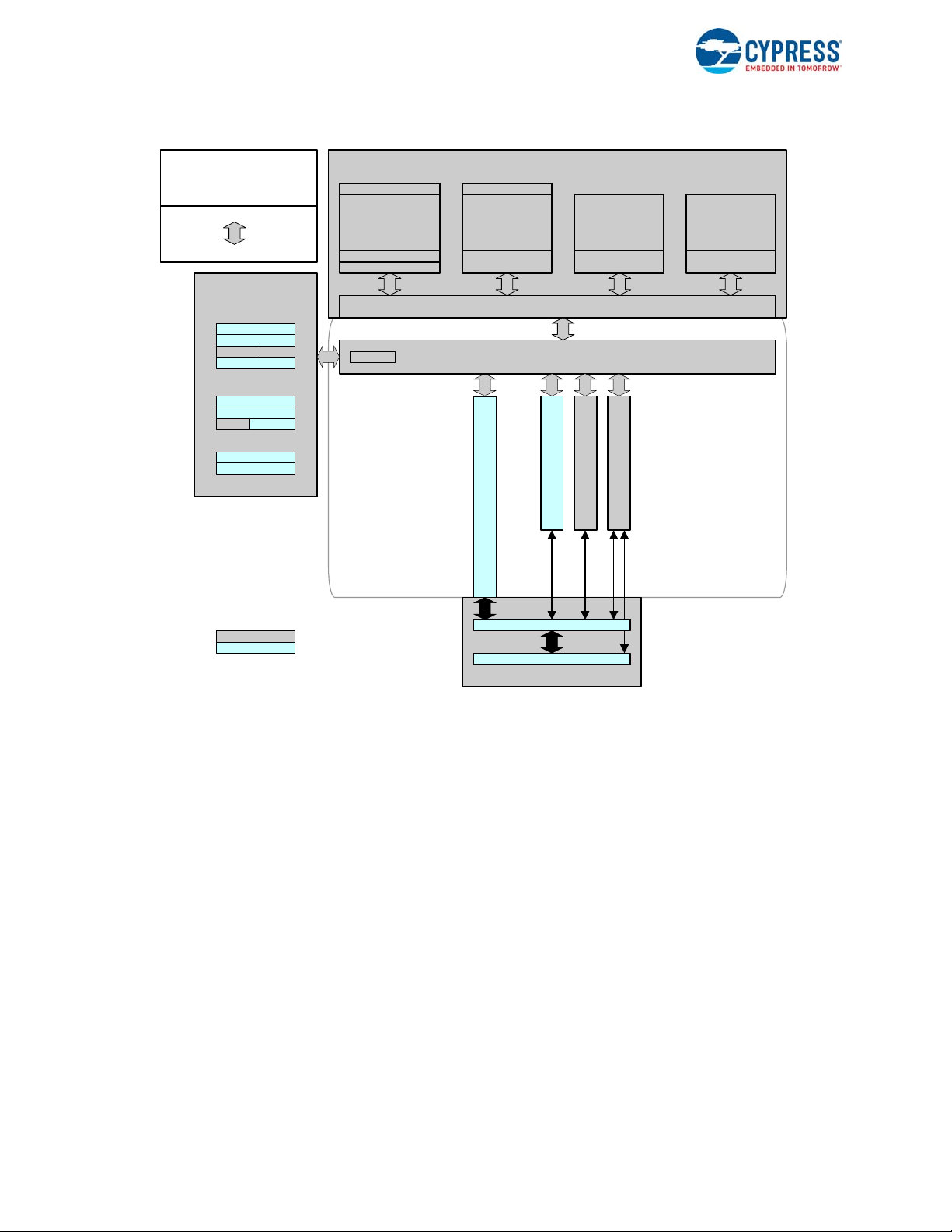
Figure 1-1 shows the major components of the PSoC 4000 architecture.
®
)
PSoC 4000 Family: PSoC 4 Architecture TRM, Document No. 001-89309 Rev. *D 13
Page 14
Introduction
Deep Sleep
Active/ Sleep
CPU Subsystem
SRAM
2 KB
SRAM Controller
ROM
4 KB
ROM Controller
Flash
16 KB
Read Accelerator
SPCIFSWD/TC
NVIC, IRQMX
Cortex
M0
16 MHz
MUL
System Interconnect (
Single/Multi Layer AHB
)
I/O Subsystem
20x GPIOs
IOS S GP IO (4x ports )
Peripherals
Peripheral Interconnect (MMIO)
PCLK
PSoC 4000
32-bit
AHB-Lite
System Resources
Lite
Power
Clock
WDT
ILO
Reset
Clock Control
IMO
Sleep Control
PWRSYS
REFPOR
WIC
Reset Control
XRES
1x SCB-I2C
CapSense
High Speed I/O Matrix
Power Modes
1x TCPWM
Figure 1-1. PSoC 4000 Family Block Diagram
1.2 Features
The PSoC 4000 family has these major components:
■ 32-bit Cortex-M0 CPU with single-cycle multiply, deliver-
ing up to 14 DMIPS at 16 MHz
■ Up to 16 KB flash and 2 KB SRAM
■ A center-aligned pulse-width modulator (PWM) with
complementary, dead-band programmable outputs
■ I2C communication block with slave, master, and multi-
master operating modes
■ CapSense
■ Low-power operating modes: Sleep and Deep-Sleep
■ Programming and debugging system through serial wire
debug (SWD)
■ Two current sourcing/sinking DACs (IDACs)
■ Comparator with 1.2 V reference
■ Fully supported by PSoC Creator™ IDE tool
1.3 CPU System
1.3.1 Processor
The heart of the PSoC 4 is a 32-bit Cortex-M0 CPU core
running up to 16 MHz for PSoC 4000. It is optimized for lowpower operation with extensive clock gating. It uses 16-bit
instructions and executes a subset of the Thumb-2 instruction set. This instruction set enables fully compatible binary
upward migration of the code to higher performance processors such as Cortex M3 and M4.
The CPU has a hardware multiplier that provides a 32-bit
result in one cycle.
1.3.2 Interrupt Controller
The CPU subsystem includes a nested vectored interrupt
controller (NVIC) with nine interrupt inputs and a wakeup
interrupt controller (WIC), which can wake the processor
from Deep-Sleep mode.
14 PSoC 4000 Family: PSoC 4 Architecture TRM, Document No. 001-89309 Rev. *D
Page 15

Introduction
1.4 Memory
The PSoC 4 memory subsystem consists of a 16 KB flash
module with a flash accelerator, 2 KB SRAM, and 4 KB
supervisory ROM options. The flash accelerator improves
the average access times from the flash block delivering
85 percent of single-cycle SRAM access performance. A
powerful and flexible protection model allows you to selectively lock blocks of memory for read and write protection,
securing sensitive information. Additionally, all device interfaces can be permanently disabled for applications concerned about phishing attacks due to a maliciously
reprogrammed device or attempts to defeat security by
starting and interrupting flash programming sequences. The
supervisory ROM is used to store the boot and configuration
routines.
1.5 System-Wide Resources
1.5.1 Clocking System
The clocking system for the PSoC 4 device consists of the
internal main oscillator (IMO) and internal low-speed oscillator (ILO) as internal clocks and has provision for an external
clock.
The system clock (SYSCLK) required for the CPU system
and the high-frequency clock (HFCLK) required by the
peripherals can be as high as 16 MHz. These clocks are
generated from the IMO.
The IMO with an accuracy of ±2 percent is the primary
source of internal clocking in the device. The default IMO
frequency is 24 MHz and it can be adjusted between 3 MHz
and 48 MHz in steps of 1 MHz. The default IMO frequency is
24 MHz and can be adjusted between 24 MHz and 48 MHz
in steps of 4 MHz. Multiple clock derivatives are generated
from the main clock frequency to meet various application
needs.
The ILO is a low-power, less accurate oscillator and is used
to generate clocks for peripheral operation in Deep-Sleep
mode. Its clock frequency is 32 kHz with ±60 percent accuracy.
An external clock source ranging from MHz to 16 MHz can
be used to generate the clock derivatives for the functiona l
blocks instead of the IMO.
frequency clock is ON and the low-frequency peripherals
are in operation.
Multiple internal regulators are available in the system to
support power supply schemes in different power modes.
1.5.3 GPIO
Every GPIO in PSoC 4 has the following characteristics:
■ Eight drive strength modes
■ Individual control of input and output disables
■ Hold mode for latching previous state
■ Selectable slew rates
■ Interrupt generation – edge triggered
The PSoC 4 also supports CapSense capability on 17 out of
20 GPIOs. The pins are organized in a port that is 8-bit wide.
A high-speed I/O matrix is used to multiplex between various signals that may connect to an I/O pin. Pin locations for
fixed-function peripherals are also fixed.
1.6 Fixed-Function Digital
1.6.1 Timer/Counter/PWM Block
The Timer/Counter/PWM block consists of a 16-bit counter
with user-programmable period length. The TCPWM block
has a capture register, period register, and compare register .
The block supports complementary, dead-band programmable outputs. It also has a kill input to force outputs to a predetermined state. Other features of the block include centeraligned PWM, clock prescaling, pseudo random PWM, and
quadrature decoding.
1.6.2 Serial Communication BlocksI2C Block
The PSoC 4 has a fixed-function I2C interface. The I2C
interface can be used for general-purpose I2C communication and for tuning the CapSense component fo r optimized
operation.
The features of the I2C block include:
■ Standard I
■ EZ function mode support with 32-byte buffer
2
C multi-master and slave function
1.5.2 Power System
The PSoC 4 operates with a single external supply in the
range 1.71 V to 5.5 V.
PSoC 4 has two low-power modes – Sleep and Deep-Sleep
– in addition to the default Active mode. In Active mode, the
CPU runs with all the logic powered. In Sleep mode, the
CPU is powered off with all other peripherals functional. In
Deep-Sleep mode, the CPU, SRAM, and high-speed logic
are in retention; the main system clock is OFF while the low-
PSoC 4000 Family: PSoC 4 Architecture TRM, Document No. 001-89309 Rev. *D 15
1.7 Special Function Peripherals
1.7.1 CapSense
PSoC 4 devices have the CapSense feature, which allows
you to use the capacitive properties of your fingers to toggle
buttons and sliders. CapSense functionality is su pported on
all but three GPIO pins in PSoC 4 through a CapSense
Sigma-Delta (CSD) block. The CSD also provides waterproofing capability.
Page 16

Introduction
1.7.1.1 IDACs and Comparator
The CapSense block has two IDACs and a comparator with
a 12-V reference, which can be used for general purposes, if
CapSense is not used.
1.8 Program and Debug
PSoC 4 devices support programming and debugging features of the device via the on-chip SWD interface. The PSoC
Creator IDE provides fully integrated programming and
debugging support. The SWD interface is also fully compatible with industry standard third-party tools.
16 PSoC 4000 Family: PSoC 4 Architecture TRM, Document No. 001-89309 Rev. *D
Page 17

2. Getting S tarted
2.1 Support
Free support for PSoC®4 products is available online at www.cypress.com/psoc4. Resources include training seminars,
discussion forums, application notes, PSoC consultants, CRM technical support email, knowledge base, and application
support engineers.
For application assistance, visit www.cypress.com/support/ or call 1-800-541-4736.
2.2 Product Upgrades
Cypress provides scheduled upgrades and version enhancements for PSoC C reator free of charge. Upgrades a re available
from your distributor on DVD-ROM; you can also download them directly from www.cypress.com/psoccreator. Critical updates
to system documentation are also provided in the Documentation section.
2.3 Development Kits
The Cypress Online Store contains development kits, C compilers, and the accessories you need to successfully develop
PSoC projects. Visit the Cypress Online Store website at www.cypress.com/cypress-store. Under Products, click Program-
mable System-on-Chip to view a list of available items. Development kits are also available from Digi-Key, Avnet, Arrow, and
Future.
2.4 Application Notes
Refer to application note AN79953 - Getting Started with PSoC 4 for additional information on PSoC 4 device capabilities and
to quickly create a simple PSoC application using PSoC Creator and PSoC 4 development kits.
PSoC 4000 Family: PSoC 4 Architecture TRM, Document No. 001-89309 Rev. *D 17
Page 18

Getting Started
18 PSoC 4000 Family: PSoC 4 Architecture TRM, Document No. 001-89309 Rev. *D
Page 19

3. Document Construction
This document includes the following sections:
■ Section B: CPU System on page 23
■ Section D: System Resources Subsystem (SRSS) on page 43
■ Section E: Digital System on page 81
■ Section F: Analog System on page 125
■ Section G: Program and Debug on page 137
3.1 Major Sections
For ease of use, information is organized into sections and chapters that are divided according to device functionality.
■ Section – Presents the top-level architecture, how to get started, and conventions and overview information of the prod-
uct.
■ Chapter – Presents the chapters specific to an individual aspect of the section topic. These are the detailed implementa-
tion and use information for some aspect of the integrated circuit.
■ Glossary – Defines the specialized terminology used in this technical reference manual (TRM). Glossary terms are pre-
sented in bold, italic font throughout.
■ Registers Technical Reference Manual – Supplies all device register details summarized in the technical reference man-
ual. This is an additional document.
3.2 Documentation Conventions
This document uses only four distinguishing font types, besides those found in the headings.
■ The first is the use of italics when referencing a document title or file name.
■ The second is the use of bold italics when referencing a term described in the Glossary of this document.
■ The third is the use of Times New Roman font, distinguishing equation examples.
■ The fourth is the use of Courier New font, distinguishing code examples.
3.2.1 Register Conventions
Register conventions are detailed in the PSoC 4000 Family: PSoC 4 Registers TRM.
3.2.2 Numeric Naming
Hexadecimal numbers are represented with all letters in u ppercase with an appended lowercase ‘h’ (for example, ‘14h’ or
‘3Ah’) and hexadecimal numbers may also be represented by a ‘0x’ prefix, the C coding convention. Binary numbers have an
appended lowercase ‘b’ (for example, 01010100b’ or ‘01000011b’). Numbers not indicated by an ‘h’ or ‘b’ are decimal.
PSoC 4000 Family: PSoC 4 Architecture TRM, Document No. 001-89309 Rev. *D 19
Page 20

Document Construction
3.2.3 Units of Measure
This table lists the units of measure used in this document.
Table 3-1. Units of Measure
Abbreviation Unit of Measure
bps bits per second
°C degrees Celsius
dB decibels
fF femtofarads
Hz Hertz
k kilo, 1000
K kilo, 2^10
KB 1024 bytes, or approximately one thousand bytes
Kbit 1024 bits
kHz kilohertz (32.000)
k kilohms
MHz megahertz
M megaohms
µA microamperes
µF microfarads
µs microseconds
µV microvolts
µVrms microvolts root-mean-square
mA milliamperes
ms milliseconds
mV millivolts
nA nanoamperes
ns nanoseconds
nV nanovolts
ohms
pF picofarads
pp peak-to-peak
ppm parts per million
SPS samples per second
sigma: one standard deviation
V volts
3.2.4 Acronyms
This table lists the acronyms used in this document
Table 3-2. Acronyms
Acronym Definition
ABUS analog output bus
AC alternating current
ADC analog-to-digital converter
AHB
API application programming interface
AMBA (advanced microcontroller bus architecture)
high-performance bus, an ARM data transfer bus
Table 3-2. Acronyms (continued)
Acronym Definition
APOR analog power-on reset
BC broadcast clock
BOD brownout detect
BOM bill of materials
BR bit rate
BRA bus request acknowledge
BRQ bus request
CAN controller area network
CI carry in
CMP compare
CO carry out
CPU central processing unit
CRC cyclic redundancy check
CSD CapSense sigma delta
CT continuous time
CTB continuous time block
CTBm continuous time block mini
DAC digital-to-analog converter
DAP debug access port
DC direct current
DI digital or data input
DMA direct memory access
DNL differential nonlinearity
DO digital or data output
DSI digital signal interface
DSM deep-sleep mode
DW data wire
ECO external crystal oscillator
EEPROM
EMIF external memory interface
FB feedback
FIFO first in first out
FSR full scale range
GPIO general purpose I/O
HCI host-controller interface
HFCLK high-frequency clock
HSIOM high-speed I/O matrix
I2C
IDE integrated development environment
ILO internal low-speed oscillator
ITO indium tin oxide
IMO internal main oscillator
INL integral nonlinearity
I/O input/output
IOR I/O read
IOW I/O write
electrically erasable programmable read only
memory
inter-integrated circuit
20 PSoC 4000 Family: PSoC 4 Architecture TRM, Document No. 001-89309 Rev. *D
Page 21
Document Construction
Table 3-2. Acronyms (continued)
Acronym Definition
IRES initial power on reset
IRA interrupt request acknowledge
IRQ interrupt request
ISR interrupt service routine
IVR interrupt vector read
LCD liquid crystal display
LFCLK low-frequency clock
LPCOMP low-power comparator
LRb last received bit
LRB last received byte
LSb least significant bit
LSB least significant byte
LUT lookup table
MISO master-in-slave-out
MMIO memory mapped input/output
MOSI master-out-slave-in
MSb most significant bit
MSB most significant byte
NMI non-maskable interrupt
NVIC nested vectored interrupt controller
PC program counter
PCB printed circuit board
PCH program counter high
PCL program counter low
PD power down
PGA programmable gain amplifier
PM power management
PMA PSoC memory arbiter
POR power-on reset
PPOR precision power-on reset
PRS pseudo random sequence
®
PSoC
PSRR power supply rejection ratio
PSSDC power system sleep duty cycle
PWM pulse width modulator
RAM random-access memory
RETI return from interrupt
RF radio frequency
ROM read only memory
RMS root mean square
RW read/write
SAR successive approximation register
SC switched capacitor
SCB serial communication block
SIE serial interface engine
SIO special I/O
SE0 single-ended zero
Programmable System-on-Chip
Table 3-2. Acronyms (continued)
Acronym Definition
SNR signal-to-noise ratio
SOF start of frame
SOI start of instruction
SP stack pointer
SPD sequential phase detector
SPI serial peripheral interconnect
SPIM serial peripheral interconnect master
SPIS serial peripheral interconnect slave
SRAM static random-access memory
SROM supervisory read only memory
SSADC single slope ADC
SSC supervisory system call
SYSCLK system clock
SWD single wire debug
TC terminal count
TCPWM timer, counter, PWM
TD transaction descriptors
UART universal asynchronous receiver/transmitter
UDB universal digital block
USB universal serial bus
USBIO USB I/O
WCO watch crystal oscillator
WDT watchdog timer
WDR watchdog reset
XRES external reset
XRES_N external reset, active low
PSoC 4000 Family: PSoC 4 Architecture TRM, Document No. 001-89309 Rev. *D 21
Page 22

Document Construction
22 PSoC 4000 Family: PSoC 4 Architecture TRM, Document No. 001-89309 Rev. *D
Page 23
Section B: CPU System
SWD/TC
Cortex-M0
16 MHz (14 DMIPS)
NVIC, IRQMX
System Interconnect (Single Layer AHB)
This section encompasses the following chapters:
■ Cortex-M0 CPU chapter on page 25
■ Interrupt schapter on page 31
Top Level Architecture
CPU System Block Diagram
PSoC 4000 Family: PSoC 4 Architecture TRM, Document No. 001-89309 Rev. *D 23
Page 24

24 PSoC 4000 Family: PSoC 4 Architecture TRM, Document No. 001-89309 Rev. *D
Page 25

4. Cortex-M0 CPU
The PSoC® 4 ARM Cortex-M0 core is a 32-bit CPU optimized for low-power operation. It has an efficient three-stage pipeline,
a fixed 4-GB memory map, and supports the ARMv6-M Thumb instruction set. The Cortex-M0 also features a single-cycle 32bit multiply instruction and low-latency interrupt handling. Other subsystems tightly linked to the CPU core include a nested
vectored interrupt controller (NVIC), a SYSTICK timer, and debug.
This section gives an overview of the Cortex-M0 processor. For more details, see the ARM Cortex-M0 user guide or technical
reference manual, both available at www.arm.com.
4.1 Features
The PSoC 4 Cortex-M0 has the following features:
■ Easy to use, program, and debug, ensuring easier migration from 8- and 16-bit processors
■ Operates at up to 0.9 DMIPS/MHz; this helps to increase execution speed or reduce power
■ Supports the Thumb instruction set for improved code density, ensuring efficient use of memory
■ NVIC unit to support interrupts and exceptions for rapid and deterministic interrupt response
■ Extensive debug support including:
❐ SWD port
❐ Breakpoints
❐ Watchpoints
PSoC 4000 Family: PSoC 4 Architecture TRM, Document No. 001-89309 Rev. *D 25
Page 26
Cortex-M0 CPU
ARM Cortex-M0 CPU
Sys te m I nte rco nne c t
Flash
Accelerator
SRAM
Controller
SROM
Controller
DAP
CPU Subsystem
Flash SRAM SROM
AHB Br idge
Test
Controller
Fixed In t er r up t s
DS I Inter rupts
Flash
Programming
Interface
CPU & Memory
Subsystem
Interrupt
MUX
4.2 Block Diagram
Figure 4-1. PSoC 4 CPU Subsystem Block Diagram
4.3 How It Works
The Cortex-M0 is a 32-bit processor with a 32-bit data path, 32-bit registers, and a 32-bit memory interf ace. It supports most
16-bit instructions in the Thumb instruction set and some 32-bit instructions in the Thumb-2 instruction set.
The processor supports two operating modes (see “Operating Modes” on page 28). It has a single-cycle 32-bit multiplication
instruction.
4.4 Address Map
The ARM Cortex-M0 has a fixed address map allowing access t o memory and peripherals using simple memory access
instructions. The 32-bit (4 GB) address space is divided into the regions show n in Table 4-1. Note that code can be executed
from the code and SRAM regions.
Table 4-1. Cortex-M0 Address Map
Address Range Name Use
0x00000000 - 0x1FFFFFFF Code
0x20000000 - 0x3FFFFFFF SRAM Data region. You can also execute code from this region.
0x40000000 - 0x5FFFFFFF Peripheral All peripheral registers. You cannot execute code from this region.
0x60000000 - 0xDFFFFFFF Not used.
0xE0000000 - 0xE00FFFFF PPB Peripheral registers within the CPU core.
0xE0100000 - 0xFFFFFFFF Device PSoC 4 implementation-specific.
Program code region. You can also place data here. Includes the exception vector table,
which starts at address 0.
26 PSoC 4000 Family: PSoC 4 Architecture TRM, Document No. 001-89309 Rev. *D
Page 27

Cortex-M0 CPU
4.5 Registers
The Cortex-M0 has 16 32-bit registers, as Table 4-2 shows:
■ R0 to R12 – General-purpose registers. R0 to R7 can be accessed by all instructions; the other registers can be accessed
by a subset of the instructions.
■ R13 – Stack pointer (SP). There are two stack pointers, with only one available at a t i me. In th re ad mode, the CONTROL
register indicates the stack pointer to use, Main Stack Pointer (MSP) or Process Stack Pointer (PSP).
■ R14 – Link register. Stores the return program counter during function calls.
■ R15 – Program count er. This register can be written to contro l program flow.
Table 4-2. Cortex-M0 Registers
Name
R0-R12 RW Undefined R0-R12 are 32-bit general-purpose registers for data operations.
MSP (R13)
PSP (R13)
LR (R14) RW Undefined
PC (R15) RW [0x00000004]
PSR RW Undefined
APSR RW Undefined
EPSR RO [0x00000004].0 On reset, EPSR is loaded with the value bit[0] of the register [0x00000004].
IPSR RO 0 The IPSR contains the exception number of the current ISR.
PRIMASK RW 0 The PRIMASK register prevents activation of all exceptions with configurable priority.
CONTROL RW 0 The CONTROL register controls the stack used when the processor is in thread mode.
a. Describes access type during program execution in thread mode and handler mode. Debug access can differ.
a
Type
RW [0x00000000]
Reset Value Description
The stack pointer (SP) is register R13. In thread mode, bit[1] of the CONTROL register
indicates which stack pointer to use:
0 = Main stack pointer (MSP). This is the reset value.
1 = Process stack pointer (PSP).
On reset, the processor loads the MSP with the value from address 0x00000000.
The link register (LR) is register R14. It stores the return information for subroutines,
function calls, and exceptions.
The program counter (PC) is register R15. It contains the current program address. On
reset, the processor loads the PC with the value from address 0x00000004. Bit[0] of the
value is loaded into the EPSR T-bit at reset and must be 1.
The program status register (PSR) combines:
Application Program Status Register (APSR).
Execution Program Status Register (EPSR).
Interrupt Program Status Register (IPSR).
The APSR contains the current state of the condition flags from previous instruction
executions.
Table 4-3 shows how the PSR bits are assigned.
Table 4-3. Cortex-M0 PSR Bit Assignments
Bit PSR Register Name Usage
31 APSR N Negative flag
30 APSR Z Zero flag
29 APSR C Carry or borrow flag
28 APSR V Overflow flag
PSoC 4000 Family: PSoC 4 Architecture TRM, Document No. 001-89309 Rev. *D 27
Page 28

Cortex-M0 CPU
Table 4-3. Cortex-M0 PSR Bit Assignments
Bit PSR Register Name Usage
27 – 25 – – Reserved
24 EPSR T
23 – 6 – – Reserved
5 – 0 IPSR N/A
Thumb state bit. Must always be 1. Attempting to execute instructions when the T bit is 0
results in a HardFault exception.
Exception number of current ISR:
0 = thread mode
1 = reserved
2 = NMI
3 = HardFault
4 – 10 = reserved
11 = SVCall
12, 13 = reserved
14 = PendSV
15 = SysTick
16 = IRQ0
…
24 = IRQ8
Use the MSR or CPS instruction to set or clear bit 0 of th e PRIM ASK regi ster. If the bit is 0, exceptions are enabled. If the bit
is 1, all exceptions with configurable priority, that is, all exceptions except HardFault, NMI, and Reset, are disabled. See th e
Interrupts chapter on page 31 for a list of exceptions.
4.6 Operating Modes
The Cortex-M0 processor supports two operating modes:
■ Thread Mode – used by all normal applications. In this mode, the MSP or PSP can be used. The CONTROL register bit 1
determines which stack pointer is used:
❐ 0 = MSP is the current stack pointer
❐ 1 = PSP is the current stack pointer
■ Handler Mode – used to execute exception handlers. The MSP is always used.
In thread mode, use the MSR instruction to set the stack pointer bit in the CONTROL register. When changing the stack
pointer, use an ISB instruction immediately after the MSR instruction. This ensures that instructions after the ISB execute
using the new stack pointer.
In handler mode, explicit writes to the CONTROL register are ignored, because the MSP is always used. The exception entry
and return mechanisms automatically update the CONTROL register.
4.7 Instruction Set
The Cortex-M0 implements a version of the Thumb instruction set, as Table4-4 shows. For details, see the Cortex-M0
Generic User Guide.
An instruction operand can be an ARM register, a constant, or another instruction-specific parameter. Instructions act on the
operands and often store the result in a destinat ion register. Many instructions a re unable to use, or have restrictions on
using, the PC or SP for the operands or destination register.
28 PSoC 4000 Family: PSoC 4 Architecture TRM, Document No. 001-89309 Rev. *D
Page 29

Cortex-M0 CPU
Table 4-4. Thumb Instruction Set
Mnemonic Brief Description
ADCS Add with carry
a
ADD{S}
ADR PC-relative address to register
ANDS Bit wise AND
ASRS Arithmetic shift right
B{cc} Branch {conditionally}
BICS Bit clear
BKPT Breakpoint
BL Branch with link
BLX Branch indirect with link
BX Branch indirect
CMN Compare negative
CMP Compare
CPSID Change processor state, disable interrupts
CPSIE Change processor state, enable interrupts
DMB Data memory barrier
DSB Data synchronization barrier
EORS Exclusive OR
ISB Instruction synchronization barrier
LDM Load multiple registers, increment after
LDR Load register from PC-relative address
LDRB Load register with word
LDRH Load register with half-word
LDRSB Load register with signed byte
LDRSH Load register with signed half-word
LSLS Logical shift left
LSRS Logical shift right
a
MOV{S}
MRS Move to general register from special register
MSR Move to special register from general register
MULS Multiply, 32-bit result
MVNS Bit wise NOT
NOP No operation
ORRS Logical OR
POP Pop registers from stack
PUSH Push registers onto stack
REV Byte-reverse word
REV16 Byte-reverse packed half-words
REVSH Byte-reverse signed half-word
RORS Rotate right
RSBS Reverse subtract
SBCS Subtract with carry
Add
Move
Table 4-4. Thumb Instruction Set
Mnemonic Brief Description
SEV Send event
STM Store multiple registers, increment after
STR Store register as word
STRB Store register as byte
STRH Store register as half-word
a
SUB{S}
SVC Supervisor call
SXTB Sign extend byte
SXTH Sign extend half-word
TST Logical AND-based test
UXTB Zero extend a byte
UXTH Zero extend a half-word
WFE Wait for event
WFI Wait for interrupt
a. The ‘S’ qualifier causes the ADD, SUB, or MOV instructions to update
APSR condition flags.
Subtract
4.7.1 Address Alignment
An aligned access is an operation where a word-aligned
address is used for a word or multiple word access, or
where a half-word-aligned address is used for a half-word
access. Byte accesses are always aligned.
No support is provided for unaligned accesses on the Cortex-M0 processor. Any attempt to perform an unaligned
memory access operation results in a HardFault exception.
4.7.2 Memory Endianness
The PSoC 4 Cortex-M0 uses the little-endian forma t, where
the least-significant byte of a word is stored at the lowest
address and the most significant byte is stored at the hi ghest address.
4.8 Systick Timer
The Systick timer is integrated with the NVIC and ge nerates
the SYSTICK interrupt. This interrupt can be used for task
management in a real-time system. The timer has a reload
register with 24 bits available to use as a countdown value.
The Systick timer uses the Cortex-M0 internal clock as a
source.
4.9 Debug
PSoC 4 contains a debug interface based on SWD; it features four breakpoint (address) comparators and two watchpoint (data) comparators.
PSoC 4000 Family: PSoC 4 Architecture TRM, Document No. 001-89309 Rev. *D 29
Page 30

Cortex-M0 CPU
30 PSoC 4000 Family: PSoC 4 Architecture TRM, Document No. 001-89309 Rev. *D
Page 31

5. Interrupts
Nested
Vectored
Interrupt
Controller
(NVIC)
Cortex-M0
Processor Core
IRQ0
Cortex-M0 Processor
IRQ1
IRQ8
Interrupt signals
from PSoC 4
on-chip peripherals
The ARM Cortex-M0 (CM0) CPU in PSoC® 4 supports interrupts and exceptions. Interrupts refer to those events generated
by peripherals external to the CPU such as timers, serial communication block, and port pin signals. Exceptions refer to those
events that are generated by the CPU such as memory access faults and internal system timer events. Both interrupts and
exceptions result in the current program flow being stopped and the exception handler or interrupt service routine (ISR) being
executed by the CPU. The device provides a unified exception vector table for both interrupt handlers/ISR and exception handlers.
5.1 Features
PSoC 4 supports the following interrupt features:
■ Supports 9 interrupts
■ Nested vectored interrupt controller (NVIC) integrated with CPU core, yielding low interrupt latency
■ Vector table may be placed in either flash or SRAM
■ Configurable priority levels from 0 to 3 for each interrupt
■ Level-triggered and pulse-triggered interrupt signals
5.2 How It Works
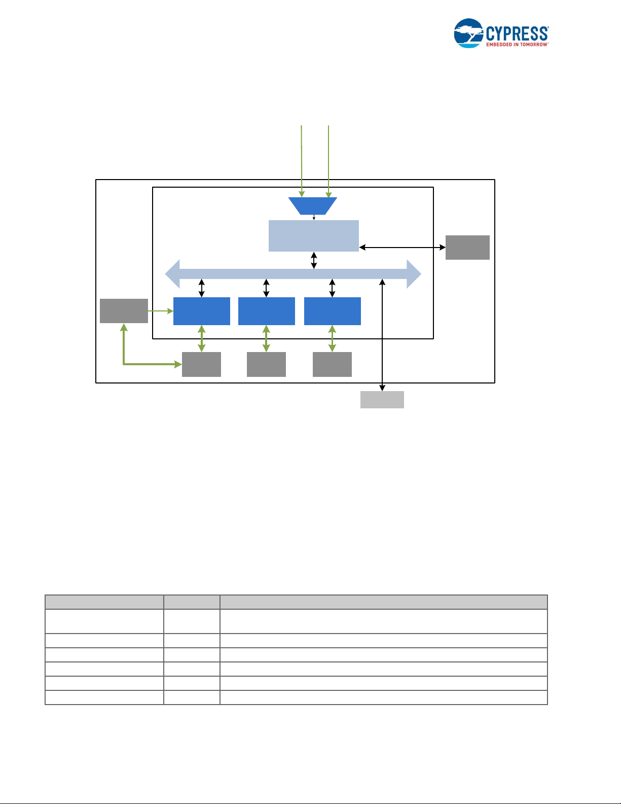
Figure 5-1. PSoC 4 Interrupts Block Diagram
Figure 5-1 shows the interacti on between interrupt sign als and the Cortex-M0 CPU. PSoC 4 h as nine inte rrupts; these inter-
rupt signals are processed by the NVIC. The NVIC takes care of enabling/disabling individual inte rrupts, priority resolution,
and communication with the CPU core. The except ions are not shown in Figure 5-1 because they are part of CM0 core generated events, unlike interrupts, which are generated by peripherals external to the CPU.
PSoC 4000 Family: PSoC 4 Architecture TRM, Document No. 001-89309 Rev. *D 31
Page 32

Interrupts
Rising Edge on Interrupt Line is
registered by the NVIC
CPU detects the request signal
from NVIC and stores its
current context by pushing
conte nts onto the stack
CPU receives exception
number of triggered interrupt
and fetches the address of the
specific exception handle from
vector table.
CPU branches to the received
address and executes
exception handler
CPU registers are restored
using stack upon completion of
exception handler.
IRQn
CPU
Execution
State
main
ISR ISR
main
ISR
main
IRQn is still high
IRQn
CPU
Execution
State
main
ISR
main
ISR
main
ISR
5.3 Interrupts and Exceptions Operation
5.3.1 Interrupt/Exception Handling
The following sequence of events occurs when an interrupt
or exception event is triggered:
1. Assuming that all the interrupt signals are initially low
(idle or inactive state) and the processor is executing the
main code, a rising edge on any one of the interrupt lines
is registered by the NVIC. The interrupt line is now in a
pending state waiting to be serviced by the CPU.
2. On detecting the interrupt request signal from the NVIC,
the CPU stores its current context by pushing the contents of the CPU registers onto the stack.
3. The CPU also receives the exception number of the trig-
gered interrupt from the NVIC. All interrupts and exceptions have a unique exception number, as given in
Table 5-1. By using this exception number, the CPU
fetches the address of the specific exception handler
from the vector table.
4. The CPU then branches to this address and executes
the exception handler that follows.
5. Upon completion of the exception handler, the CPU reg-
isters are restored to their original state using stack pop
operations; the CPU resumes the main code execution.
Figure 5-2. Interrupt Handling When Triggered
When the NVIC receives an interrupt request while another
interrupt is being serviced or receives multiple interrupt
requests at the same time, it evaluates the priority of all
these interrupts, sending the exception number of the hig hest priority interrupt to the CPU. Thus, a higher priority interrupt can block the execution of a lower priority ISR at any
time.
Exceptions are handled in the same way that interrupts are
handled. Each exception event has a unique exception number, which is used by the CPU to execute the appropriate
exception handler.
5.3.2 Level and Pulse Interrupts
NVIC supports both level and pulse signals on the interrupt
lines (IRQ0 to IRQ8). The classification of an interrupt as
level or pulse is based on the interrupt source.
Figure 5-3. Level Interrupts
Figure 5-4. Pulse Interrupts
Figure 5-3 and Figure 5-4 show the working of level and
pulse interrupts, respectively. Assuming the interrupt signal
is initially inactive (logic low), the following sequence of
events explains the handling of level and pulse interrupts:
1. On a rising edge event of the interrupt signal, the NVIC
registers the interrupt request. The interrupt is now in the
pending state, which means the interrupt requests have
not yet been serviced by the CPU.
2. The NVIC then sends the exception number along with
the interrupt request signal to the CPU. When the CPU
starts executing the ISR, the pending state of the interrupt is cleared.
3. When the ISR is being executed by the CPU, one or
more rising edges of the interrupt signal are logged as a
single pending request. The pending interrupt is serviced
again after the current ISR exe cu ti o n is complete (see
Figure 5-4 for pulse interrupts).
4. If the interrupt signal is still high after completing the ISR,
it will be pending and the ISR is executed again.
Figure 5-3 illustrates this for level triggered interrupts,
where the ISR is executed as long as the interrupt signal
is high.
32 PSoC 4000 Family: PSoC 4 Architecture TRM, Document No. 001-89309 Rev. *D
Page 33

Interrupts
5.3.3 Exception Vector Table
The exception vector table (Table 5-1), stores t he entry point addresses for all exception handlers. The CPU fetches the
appropriate address based on the exception number.
Table 5-1. Exception Vector Table
Exception Number Exception Exception Priority Vector Address
– Initial Stack Pointer Value Not applicable (NA)
1 Reset –3, the highest priority Base_Address + 0x04
2 Non Maskable Interrupt (NMI) –2 Base_Address + 0x08
3 HardFault –1 Base_Address + 0x0C
4-10 Reserved NA Base_Address + 0x10 to Base_Address + 0x28
11 Supervisory Call (SVCall) Configurable (0 - 3) Base_Address + 0x2C
12-13 Reserved NA Base_Address + 0x30 to Base_Address + 0x34
14 PendSupervisory (PendSV) Configurable (0 - 3) Base_Address + 0x38
15 System Timer (SysTick) Configurable (0 - 3) Base_Address + 0x3C
16 External Interrupt(IRQ0) Configurable (0 - 3) Base_Address + 0x40
… … Configurable (0 - 3) …
24 External Interrupt(IRQ8) Configurable (0 - 3) Base_Address + 0x52
Base_Address - 0x00000000 (start of flash memory) or
0x20000000 (start of SRAM)
In Table 5-1, the first word (4 bytes) is not marked as excep-
tion number zero. This is because the first word in the
exception table is used to initialize the main stack pointer
(MSP) value on device reset; it is not considered as an
exception. In PSoC 4, the vector table can be configured t o
be located either in flash memory (base address of
0x00000000) or SRAM (base address of 0x20000000). This
configuration is done by writing to the VECT_IN_RAM bit
field (bit 0) in the CPUSS_CONFIG register. When the
VECT_IN_RAM bit field is ‘1’, CPU fetches exception handler addresses from the SRAM vector table location. When
this bit field is ‘0’ (reset state), the vector table in flash memory is used for exception address fetches. You must set the
VECT_IN_RAM bit field as part of the device boot code to
configure the vector table to be in SRAM. The advantage of
moving the vector table to SRAM is that the exception handler addresses can be dynamically changed by modifying
the SRAM vector table contents. However, the nonvolatile
flash memory vector table must be modified by a flash memory write.
Reads of flash addresses 0x00000000 and 0x00000004 are
redirected to the first eight bytes of SROM to fe tch the stack
pointer and reset vectors, unless the NO_RST_OVR bit of
the CPUSS_SYSREQ register is set. To allow flash read
from addresses 0x00000000 and 0x00000004, the
NO_RST_OVR bit should be set to ‘1’. The stack pointer
vector holds the address that the stack pointer is loaded with
on reset. The reset vector holds the address of the boot
sequence. This mapping is done to use the default
addresses for the stack pointer and reset vector from SROM
when the device reset is released. For reset, boot code in
SROM is executed first and then the CPU j umps to address
0x00000004 in flash to execute the handler in flash. The
reset exception address in the SRAM vector table is never
used because VECT_IN_RAM is 0 on reset.
Also, when the SYSREQ bit of the CPUSS_SYSREQ register is set, reads of flash address 0x00000008 are redirected
to SROM to fetch the NMI vector address instead of from
flash. Reset CPUSS_SYSREQ to read the flash at address
0x00000008.
The exception sources (exception numbers 1 to 15) are
explained in 5.4 Exception Sources. The exceptions marked
as Reserved in Table 5-1 are not used, although they have
addresses reserved for them in the vector table. The interrupt sources (exception numbers 16 to 24) are explained in
5.5 Interrupt Sources.
5.4 Exception Sources
This section explains the different exception sources listed
in Table 5-1 (exception numbers 1 to 15).
5.4.1 Reset Exception
Device reset is treated as an exception in PSoC 4. It is
always enabled with a fixed priority of –3, the highest priority
exception. A device reset can occur due to multiple reasons,
such as power-on-reset (POR), external reset signal on
XRES pin, or watchdog reset. When the device is reset, the
initial boot code for configuring the device is executed out of
supervisory read-only memory (SROM). The boot code and
other data in SROM memory are programmed by Cypress,
and are not read/write accessible to external users. After
completing the SROM boot sequence, the CPU code execution jumps to flash memory. Flash memory address
0x00000004 (Exception#1 in Table 5-1) stores the location
PSoC 4000 Family: PSoC 4 Architecture TRM, Document No. 001-89309 Rev. *D 33
Page 34

Interrupts
of the startup code in flash memory. The CPU starts executing code out of this address. Note that the reset exception
address in the SRAM vector table will never be used
because the device comes out of reset with the flash vector
table selected. The register configuration to select the
SRAM vector table can be done only as part of the startup
code in flash after the reset is de-asserted.
5.4.2 Non-Maskable Interrupt (NMI) Exception
Non-maskable interrupt (NMI) is the highest priority exception other than reset. It is always enabled with a fixed priority
of –2. There are two ways to trigger an NMI exception in the
device:
■ NMI exception by setting NMIPENDSET bit (user NMI
exception):
ware by setting the NMIPENDSET bit in the interrupt
control state register (CM0_ICSR register). Setting this
bit will execute the NMI handler pointed to by the active
vector table (flash or SRAM vector table).
■ System Call NMI exception: This exception is used for
nonvolatile programming operations such as flash write
operation and flash checksum operation. It is triggered
by setting the SYSCALL_REQ bit in the
CPUSS_SYSREQ register. An NMI exception triggered
by SYSCALL_REQ bit always executes the NMI exception handler code that resides in SROM. Flash or SRAM
exception vector table is not used for system call NMI
exception. The NMI handler code in SROM is not read/
write accessible because it contains nonvolatile programming routines that should not be modified by the
user.
An NMI exception can be triggered in soft-
5.4.3 HardFault Exception
supervisor call that requires privileged access to the system.
Note that the CM0 in PSoC 4 uses a privileged mode for the
system call NMI exception, which is not related to the SVCall
exception. (See the Chip Operational Modes chapter on
page 73 for details on privileged mode.) There is no other
privileged mode support for SVCall at the architecture level
in the device. The application developer must define the
SVCall exception handler according to the end application
requirements.
The priority of a SVCall exception can be configured to a
value between 0 and 3 by writing to the two bit fields
PRI_11[31:30] of the System Handler Priority Register 2
(SHPR2). When the SVC instruction is executed, the SVCall
exception enters the pending state and waits to be serviced
by the CPU. The SVCALLPENDED bit in the System Handler Control and State Register (SHCSR) can be used to
check or modify the pending status of the SVCall exception.
5.4.5 PendSV Exception
PendSV is another supervisor call related exception similar
to SVCall, normally being software-generated. PendSV is
always enabled and its priority is configurable. The PendSV
exception is triggered by setting the PENDSVSET bit in the
Interrupt Control State Register, CM0_ICSR. On settin g this
bit, the PendSV exception enters the pending state, and
waits to be serviced by the CPU. The pending state of a
PendSV exception can be cleared by setting the PENDSVCLR bit in the Interrupt Control State Register, CM0_ICSR.
The priority of a PendSV exception can be configured to a
value between 0 and 3 by writing to the two bit fields
PRI_14[23:22] of the System Handler Priority Register 3
(CM0_SHPR3). See the ARMv6-M Architecture Reference
Manual for more details.
HardFault is an always-enabled exception that occurs
because of an error during normal or exception processing .
HardFault has a fixed priority of –1, meaning it has hig her
priority than any exception with configurable priority. HardFault exception is a catch-all exception for different types of
fault conditions, which include executing an undefined
instruction and accessing an invalid memory addresses.
The CM0 CPU does not provide fault status information to
the HardFault exception handler, but it does permit the h andler to perform an exception return and continue execution
in cases where software has the ability to recover from the
fault situation.
5.4.4 Supervisor Call (SVCall) Exception
Supervisor Call (SVCall) is an always-enabled exception
caused when the CPU executes the SVC instruction as part
of the application code. Application software uses the SVC
instruction to make a call to an underlying operating syst em
and provide a service. This is known as a supervisor call.
The SVC instruction enables the application to issue a
34 PSoC 4000 Family: PSoC 4 Architecture TRM, Document No. 001-89309 Rev. *D
Page 35

Interrupts
5.4.6 SysTick Exception
CM0 CPU in PSoC 4 supports a system timer, referred to as
SysTick, as part of its internal architecture. SysTick provides
a simple, 24-bit decrementing counter for various timekeeping purposes such as an RTOS tick timer, high-speed alarm
timer, or simple counter. The SysTick timer can be configured to generate an interrupt when its count value reaches
zero, which is referred to as SysTick exception. The exception is enabled by setting the TICKINT bit in the SysTick
Control and Status Register (CM0_SYST_CSR). The priority
of a SysTick exception can be configured to a value
between 0 and 3 by writing to the two bit fields
PRI_15[31:30] of the System Handler Priority Register 3
(SHPR3). The SysTick exception can always be generated
in software at any instant by writing a one to the PENDSTSETb bit in the Interrupt Control State Register, CM0_ICSR.
Similarly, the pending state of the SysTick exception can be
cleared by writing a one to the PENDSTCLR bit in the I nterrupt Control State Register, CM0_ICSR.
5.5 Interrupt Sources
PSoC 4 supports nine interrupts (IRQ0 to IRQ8 or exception
numbers 16 – 24) from peripherals. The source of each
interrupt is listed in Table 5-3. PSoC 4 provides flexible
sourcing options for each of the nine interrupt lines. The
interrupts include standard interrupts from the on-chip
peripherals such as TCPWM serial communication block,
CSD block, and interrupts from ports. The interrupt generated is usually the logical OR of the different peripheral
states. The peripheral status register should be read in the
ISR to detect which condition generated the interrupt. These
interrupts are usually level interrupts, which require that the
peripheral status register be read in the ISR to clear the
interrupt. If the status register is not read in the ISR, the
interrupt will remain asserted and the ISR will be executed
continuously.
See the I/O System chapter on page 53 for details on GPIO
interrupts.
Table 5-2. List of PSoC 4 Interrupt Sources
Interrupt
NMI (see “Exception Sources” on
page 33)
IRQ0 16 GPIO Interrupt - Port 0
IRQ1 17 GPIO Interrupt - Port 1
IRQ2 18 GPIO Interrupt - Port 2
IRQ3 19 GPIO Interrupt - Port 3
IRQ4 20 WDT (Watchdog timer) or Temp
IRQ5 21 SCB (Serial Communication Block)
IRQ6 22 SPC (System Performance Controller)
IRQ7 23 CSD (CapSense block counter overflow interrupt)
IRQ8 24 TCPWM0 (Timer/Counter/PWM 0)
Cortex-M0
Exception No.
2–
Interrupt Source
5.6 Exception Priority
Exception priority is useful for exception arbitration when
there are multiple exceptions that need to be serviced by the
CPU. PSoC 4 provides flexibility in choosing priority values
for different exceptions. All exceptions other than Reset,
NMI, and HardFault can be assigned a configurable priority
level. The Reset, NMI, and HardFault exceptions have a
fixed priority of –3, –2, and –1 respectively. In PSoC 4, lower
priority numbers represent higher priorities. This means that
the Reset, NMI, and HardFault exceptions h ave the highest
priorities. The other exceptions can be assigned a configurable priority level between 0 and 3.
handler after servicing the higher priority exception. The
CM0 CPU in PSoC 4 allows nesting of up to four exceptions.
When the CPU receives two or more exceptions requests of
the same priority, the lowest exception number is serviced
first.
The registers to configure the priority of exception numbers
1 to 15 are explained in “Exception Sources” on page 33.
The priority of the nine interrupts (IRQ0 to IRQ8) can be
configured by writing to the Interrupt Priority registers
(CM0_IPR). This is a group of four 32-bit registers with each
register storing the priority values of four interrupts, as given
in Table 5-3. The other bit fields in the register are not used.
PSoC 4 supports nested exceptions in which a higher priority exception can obstruct (interrupt) the currently active
exception handler. This pre-emption does not happen if the
incoming exception priority is the same as active exception.
The CPU resumes execution of the lower priority exception
PSoC 4000 Family: PSoC 4 Architecture TRM, Document No. 001-89309 Rev. *D 35
Page 36

Interrupts
Table 5-3. Interrupt Priority Register Bit Definitions
Bits Name Description
7:6 PRI_N0 Priority of interrupt number N.
15:14 PRI_N1 Priority of interrupt number N+1.
23:22 PRI_N2 Priority of interrupt number N+2.
31:30 PRI_N3 Priority of interrupt number N+3.
5.7 Enabling and Disabling
Interrupts
The NVIC provides registers to individually enable and disable the nine interrupts in software. If an interrupt is not
enabled, the NVIC will not process the interrupt requests on
that interrupt line. The Interrupt Set-Enable Register
(CM0_ISER) and the Interrupt Clear-Enable Register
(CM0_ICER) are used to enable and disable t he interrupts
respectively. These are 32-bit wide registers and each bit
corresponds to the same numbered interrupt. These registers can also be read in software to get the enable status of
the interrupts. Table 5-4 shows the register access properties for these two registers. Note that writing zero to these
registers has no effect.
Table 5-4. Interrupt Enable/Disable Registers
Register Operation Bit Value Comment
Interrupt Set
Enable Register
(CM0_ISER)
Interrupt Clear
Enable Register
(CM0_ICER)
Write
Read
Write
Read
The CM0_ISER and CM0_ICER registers are applicable
only for interrupts IRQ0 to IRQ8. These registers cannot be
used to enable or disable the exception numbers 1 to 11.
The 15 exceptions have their own support for enabling and
disabling, as explained in “Exception Sources” on page 33.
The PRIMASK register in Cortex-M0 (CM0) CPU can be
used as a global exception enable register to mask all the
configurable priority exceptions irrespective of whether they
are enabled. Configurable priority exceptions include all t he
exceptions except Reset, NMI, and HardFault listed in
Table 5-1. They can be configured to a priority level between
0 and 3, 0 being the highest priority and 3 being t he lowest
priority. When the PM bit (bit 0) in the PRIMASK register is
set, none of the configurable priority exceptions can be serviced by the CPU, though they can be i n the pending state
waiting to be serviced by the CPU after the PM bit is cleared.
1 To enable the interrupt
0 No effect
1 Interrupt is enabled
0 Interrupt is disabled
1 To disable the interrupt
0 No effect
1 Interrupt is enabled
0 Interrupt is disabled
5.8 Exception States
Each exception can be in one of the following states.
Table 5-5. Exception States
Exception State Meaning
The exception is not active or pending.
Inactive
Pending
Active
Active and Pending
The Interrupt Control State Register (CM0_ICSR) contains
status bits describing the various exceptions states.
■ The VECT ACTIVE bits ([8:0]) in the CM0_ICSR store the
exception number for the current executing exception.
This value is zero if the CPU does not execute any
exception handler (CPU is in thread mode). Note that the
value in VECT ACT IVE bit fields is the same as the v alue
in bits [8:0] of the Interrupt Program Status Register
(IPSR), which is also used to store the active exception
number.
■ The VECTPENDING bits ([20:12]) in the CM0_ICSR
store the exception number of the highest priority pending exception. This value is zero if there are no pending
exceptions.
■ The ISRPENDING bit (bit 22) in the CM0_ICSR indi-
cates if a NVIC generated interrupt (IRQ0 to IRQ8) is in
a pending state.
5.8.1 Pending Exceptions
When a peripheral generates an interrupt request signal to
the NVIC or an exception event occurs, the corresponding
exception enters the pending state. When the CPU starts
executing the corresponding exception handler routine, th e
exception is changed from the pending state to the acti ve
state.
The NVIC allows software pending of the nine interrupt lines
by providing separate register bits for setting and clearing
the pending states of the interrupts. The Interrupt Set-Pen ding register (CM0_ISPR) and the Interrupt Clear-Pending
register (CM0_ICPR) are used to set and clear the pe nding
status of the interrupt lines. These are 32-bit wide regist ers
and each bit corresponds to the same numbered interrupt.
Either the exception is disabled or the
enabled exception has not been triggered.
The exception request is received by the
CPU/NVIC and the exception is waiting to
be serviced by the CPU.
An exception that is being serviced by the
CPU but whose exception handler execution is not yet complete. A high-priority
exception can interrupt the execution of
lower priority exception. In this case, both
the exceptions are in the active state.
The exception is serviced by the processor
and there is a pending request from the
same source during its exception handler
execution.
36 PSoC 4000 Family: PSoC 4 Architecture TRM, Document No. 001-89309 Rev. *D
Page 37

Interrupts
Table 5-6 shows the register access properties for these two
registers. Note that writing zero to these registers has no
effect.
Table 5-6. Interrupt Set Pending/Clear Pending Registers
Register Operation
Interrupt SetPending Register
(CM0_ISPR)
Interrupt ClearPending Register
(CM0_ICPR)
Write
Read
Write
Read
Bit
Value
1
0 No effect
1 Interrupt is pending
0 Interrupt is not pending
1
0 No effect
1 Interrupt is pending
0 Interrupt is not pending
Comment
To put an interrupt to
pending state
To clear a pending
interrupt
Setting the pending bit when the same bit is already set
results in only one execution of the ISR. The pending bit can
be updated regardless of whether the corresponding
interrupt is enabled. If the interrupt is not enabled, the
interrupt line will not move to the pending state until it is
enabled by writing to the CM0_ISER register.
Note that the CM0_ISPR and CM0_ICPR registers are used
only for the nine peripheral interrupts (exception numbers
16–47). These registers cannot be used for pending the
exception numbers 1 to 11. These 15 exceptions have their
own support for pending, as explained in “Exception
Sources” on page 33.
current exception, the MSP is used for stack push/pop
operations, because the CPU is already in handler mode.
See the Cortex-M0 CPU chapter on page 35 for details.
The Cortex-M0 uses two techniques, tail chaining and late
arrival, to reduce latency in servicing exceptions. These
techniques are not visible to the external user and are part
of the internal processor architecture. For information on tail
chaining and late arrival mechanism, visit the ARM
Infocenter.
5.10 Interrupts and Low-Power Modes
PSoC 4 allows device wakeup from low-power modes when
certain peripheral interrupt requests are generated. The
Wakeup Interrupt Controller (WIC) block generates a
wakeup signal that causes the device to enter Active mo de
when one or more wakeup sources generate an interrupt
signal. After entering Active mode, the ISR of the peripheral
interrupt is executed.
The Wait For Interrupt (WFI) instruction, executed by the
CM0 CPU, triggers the transition into Sleep and Deep-Sleep
modes. The sequence of entering the different low-power
modes is detailed in the Power Modes chapter on page 75.
Chip low-power modes have two categories of fixed-function
interrupt sources:
■ Fixed-function interrupt sources that are available only in
the Active and Deep-Sleep modes (watchdog timer
interrupt, I2C interrupts, and GPIO interrupts)
■ Fixed-function interrupt sources that are available only in
the Active mode (all other fixed-function interrupts)
5.9 Stack Usage for Exceptions
When the CPU executes the main code (in thread mode)
and an exception request occurs, the CPU stores the state
of its general-purpose registers in the stack. It then starts
executing the corresponding exception ha ndler (in handler
mode). The CPU pushes the contents of the eight 32-bit
internal registers into the stack. These registers are the
Program and Status Register (PSR), ReturnAddress, Link
Register (LR or R14), R12, R3, R2, R1, and R0. Cortex-M0
has two stack pointers - MSP and PSP. Only one of the
stack pointers can be active at a time. When in thread mode,
the Active Stack Pointer bit in the Control register is used to
define the current active stack pointer. When in handler
mode, the MSP is always used as the stack pointer. The
stack pointer in Cortex-M0 always grows downwards and
points to the address that has the last pushed data.
When the CPU is in thread mode and an exception request
comes, the CPU uses the stack pointer defined in the
control register to store the general-purpose register
contents. After the stack push operations, the CPU enters
handler mode to execute the exception handler. When
another higher priority exception occurs while executing the
PSoC 4000 Family: PSoC 4 Architecture TRM, Document No. 001-89309 Rev. *D 37
Page 38

Interrupts
5.11 Exceptions – Initialization and Configuration
This section covers the different steps involved in initializing and configuring exceptions in PSoC 4.
1. Configuring the Exception Vector T able Location: The first step in using exceptions is to configure the vector table location
as required – either in flash memory or SRAM. This configuration is done by writing either a ‘1’ (SRAM vector table) or ‘0’
(flash vector table) to the VECT_IN_RAM bit field (bit 0) in the CPUSS_CONFIG register. This register write is done as
part of device initialization code.
It is recommended that the vector table be available in SRAM if the application needs to change the vector addresses
dynamically. If the table is located in flash, then a flash write operation is required to modify the vector table contents.
PSoC Creator IDE uses the vector table in SRAM by default.
2. Configuring Individual Exceptions: The next step is to configure individual exceptions required in an application.
a. Configure the exception or interrupt source; this inclu des setting up the interrupt generation conditions. The register
configuration depends on the specific exception required.
b. Define the exception handler function and write the address of the function to the exception vector table. Table 5-1
gives the exception vector table format; the exception handler address should be written to the app ropriate exception
number entry in the table.
c. Se t up the exception priority, as explained in “Exception Priority” on page 35.
d. Enable the exception, as explained in “Enabling and Disabling Interrupts” on page 36.
5.12 Registers
Table 5-7. List of Registers
Register Name Description
CM0_ISER Interrupt Set-Enable Register
CM0_ICER Interrupt Clear Enable Register
CM0_ISPR Interrupt Set-Pending Register
CM0_ICPR Interrupt Clear-Pending Register
CM0_IPR Interrupt Priority Registers
CM0_ICSR Interrupt Control State Register
CM0_AIRCR Application Interrupt and Reset Control Register
CM0_SCR System Control Register
CM0_CCR Configuration and Control Register
CM0_SHPR2 System Handler Priority Register 2
CM0_SHPR3 System Handler Priority Register 3
CM0_SHCSR System Handler Control and State Register
CM0_SYST_CSR Systick Control and Status Register
CPUSS_CONFIG CPU Subsystem Configuration Register
CPUSS_SYSREQ System Request Register
5.13 Associated Documents
■ ARMv6-M Architecture Reference Manual – This document explains the ARM Cortex-M0 architecture, including th e
instruction set, NVIC architecture, and CPU register descriptions.
38 PSoC 4000 Family: PSoC 4 Architecture TRM, Document No. 001-89309 Rev. *D
Page 39

Section C: Memory System
SPCIF
FLASH
16 KB
Read Accelerator
SRAM
2 kB
SROM
4 kB
SRAM Controller
ROM Controller
System Interconnect (Single Layer AHB)
This section presents the following chapter:
■ Memory Map chapt er on page 41
Top Level Architecture
Memory System Block Diagram
PSoC 4000 Family: PSoC 4 Architecture TRM, Document No. 001-89309 Rev. *D 39
Page 40

40 PSoC 4000 Family: PSoC 4 Architecture TRM, Document No. 001-89309 Rev. *D
Page 41

6. Memory Map
All PSoC® 4 memory (flash, SRAM, and SROM) and all registers are accessible by the CPU and in most cases by the debug
system. This chapter contains an overall map of the addresses of the memories and registers.
6.1 Features
The PSoC 4 memory system has the following features:
■ 16K bytes flash, 2K bytes SRAM
■ 4K byte SROM contains boot and configuration routines
■ ARM Cortex-M0 32-bit linear address space, with regions for code, SRAM, peripherals, and CPU internal registers
■ Flash is mapped to the Cortex-M0 code region
■ SRAM is mapped to the Cortex-M0 SRAM region
■ Peripheral registers are mapped to the Cortex-M0 peripheral region
■ The Cortex-M0 Private Peripheral Bus (PPB) region includes registers implemented in the CPU core. These include reg-
isters for NVIC, SysTick timer, and fixed-function I2C block. For more information, see the Cortex-M0 CPU chapter on
page 25.
6.2 How It Works
The PSoC 4 memory map is detailed in the following tables. For additional information, refer to the PSoC 4000 Family: PSoC
4 Registers TRM.
The ARM Cortex-M0 has a fixed address map allowing access to memory and peripherals using simple memory access
instructions. The 32-bit (4 GB) address space is divided into the regions shown in Table 6-1. Note that code can be executed
from the code and SRAM regions.
Table 6-1. Cortex-M0 Address Map
Address Range Name Use
0x00000000 – 0x1FFFFFFF Code
0x20000000 – 0x3FFFFFFF SRAM Executable region for data. You can also put code here.
0x40000000 – 0x5FFFFFFF Peripheral All peripheral registers. Code cannot be executed out of this region.
0x60000000 – 0xDFFFFFFF – Not used
0xE0000000 – 0xE00FFFFF PPB Peripheral registers within the CPU core.
0xE0100000 – 0xFFFFFFFF Device PSoC 4 implementation-specific.
Executable region for program code. You can also put data here. Includes the exception
vector table, which starts at address 0.
PSoC 4000 Family: PSoC 4 Architecture TRM, Document No. 001-89309 Rev. *D 41
Page 42

Memory Map
Table 6-2 shows the PSoC 4 address map.
Table 6-2. PSoC 4 Address Map
Address Range Use
0x00000000 - 0x00003FFF 16 KB flash
0x0FFFF000 - 0x10000000 4 KB supervisory flash
0x20000000 - 0x200007FF 2 KB SRAM
0x40100000 - 0x4011FFFF CPU subsystem registers
0x40020000 - 0x40023FFF I/O port control (high-speed I/O matrix) registers
0x40040000- -0x40043FFF I/O port registers
0x40050000- -0x4005FFFF TCPWM registers
0x40060000- -0x4006FFFF Fixed-function I2C registers
0x40080000- -0x4008FFFF CapSense registers
0x40030000- -0x4003FFFF Power, clock, reset control registers
0xE0000000 - 0xE00FFFFF Cortex-M0 PPB registers
0xF0000000 - 0xF0000FFF CoreSight ROM
42 PSoC 4000 Family: PSoC 4 Architecture TRM, Document No. 001-89309 Rev. *D
Page 43

Section D: System Resources Subsystem (SRSS)
System Resources
Power
Sleep Control
PWRSYS
REF
POR
WIC
XRES
Clock
WDT
ILO
Reset
Clock Control
IMO
Reset Cont rol
Peripheral Interconnect (MMIO)
This section encompasses the following chapters:
■ I/O System chapter on page 45
■ Clocking System chapter on page 55
■ Power Supply and Monitoring chapter on page 61
■ Chip Operational Modes chapter on page 67
■ Power Modes c hapter on page 69
■ Watchdog Timer chapter on page 73
■ Reset System chapter on page 77
■ Device Security chapter on page 79
Top Level Architecture
System-Wide Resources Block Diagram
PSoC 4000 Family: PSoC 4 Architecture TRM, Document No. 001-89309 Rev. *D 43
Page 44

44 PSoC 4000 Family: PSoC 4 Architecture TRM, Document No. 001-89309 Rev. *D
Page 45

7. I/O System
This chapter explains the PSoC® 4 I/O system, its features, architecture, operating modes, and interrupts. The GPIO pins in
PSoC 4 are grouped into ports; a port can have a maximum of eight GPIOs. PSoC 4000 family has a maximum of 20 GPIOs
arranged in four ports.
7.1 Features
The PSoC 4 GPIOs have these features:
■ Analog and digital input and output capabilities
■ Eight drive strength modes
■ Edge-triggered interrupts on rising edge, falling edge, or on both the edges, on pin basis
■ Slew rate control
■ Hold mode for latching previous state (used for retaining I/O state in Deep-Sleep mode)
■ Selectable CMOS and low-voltage LVTTL input buffer mode
■ CapSense support
7.2 GPIO Interface Overview
PSoC 4 is equipped with analog and digital peripherals. Figure 7-1 shows an overview of the routing between the peripherals
and pins.
PSoC 4000 Family: PSoC 4 Architecture TRM, Document No. 001-89309 Rev. *D 45
Page 46

I/O System
High Speed IO Matrix
(HSIOM)
GPIO
Configuration
GPIO Interrupt
GPIO Pin
Interface
GPIO Port Control
CSD
Controller
Fixed
Function
Digital
Peripherals
(TCPWM,
I2C)
CapSense
Pin
AMUXBUS-A
AMUXBUS-B
IO Cell
Figure 7-1. GPIO Interface Overview
GPIO pins are connected to I/O cells. These cells are equipped with an input buffer for the digital input, providing high input
impedance and a driver for the digital output signals. The dig ital peripherals connect to the I/O cells via the high-speed I/O
matrix (HSIOM). HSIOM contains multiplexers to connect between a peripheral selected by the user and the pin. The
CapSense block is connected to the GPIO pins through the AMUX buses.
7.3 I/O Cell Architecture
Figure 7-2 shows the I/O cell architecture. It comprises of a n input buffer and an o utput driver. This architecture is present in
every GPIO cell. It connects to the HSIOM multiplexers for the digital input and the output signa l. Analog perip heral s connect
directly to the pin.
46 PSoC 4000 Family: PSoC 4 Architecture TRM, Document No. 001-89309 Rev. *D
Page 47

Figure 7-2. I/O Cell Architecture in PSoC 4000
Digital
Logic
Slew
Control
PORT_SLOW (GPIO_PRTx_PC[25])
GPIO_PRTx_PC[3y+2:3y]
In
OE
PIN
VDD/VDDIO
VDD/VDDIO
Digital Output Path
GPIO_PRTx_DR[y]
ACTIVE_0 (TCPWM)
ACTIVE_1 (TCPWM)
ACTIVE_2 (TCPWM)
ACTIVE_3 (CSD Comparator)
DEEP_SLEEP_1 (SWD)
DEEP_SLEEP_0 (I2C)
OUTPUT ENABLE
HSIOM_PORT_SELx[4y+3:4y]
Pin Interrupt Signal
DATA
(GPIO_PRTx_INTR[y])
EDGE_SEL
(GPIO_PRTx_INTR_CFG[2y+1:2y])
I2C
DATA (GPIO_PRTx_PS[y])
INP_DIS (GPIO_PRTx_PC2[y])
Digital Input Path
Switches
HSIOM_PORT_SELx[4y+3:4y]
AMUXBUS-A (CapSense Source)
AMUXBUS-B (CapSense Shield)
Analog
HSIOM
3
4
Input Buffer
Disable
Drive
Mode
DSI
HSIOM
PORT_VTRIP_SEL (GPIO_PRTx_PC[24])
Buffer Mode Select
-------------------------CMOS
LVTTL
HSIOM_PORT_SELx[4y+3:4y]
4
IO CELL
Input Buffer
Output Driver
4
x – Port Number
y – Pin Number
VSS
VSS VSS
GPIO
Edge
Detect
I/O System
7.3.1 Digital Input Buffer
The digital input buffer provides a high-impedance buffer for
the external digital input. The buffer is enabl ed and di sabled
by the INP_DIS bit of the Port Configuration Register 2
PSoC 4000 Family: PSoC 4 Architecture TRM, Document No. 001-89309 Rev. *D 47
(GPIO_PRTx_PC2, where x is the port number). The buffer
is configurable for the following modes:
■ CMOS
■ LVTTL
Page 48

I/O System
These buffer modes are selected by the PORT_VTRIP_SEL
bit (GPIO_PRTx_PC[24]) of the Port Configuration register.
Table 7-1. Input Buffer Modes
PORT_VTRIP_SEL Input Buffer Mode
0b CMOS
1b LVTTL
The threshold values for each mode can be obtained from
the device datasheet. The output of the input buffer is connected to the HSIOM for routing to the selected peripherals.
Writing to the HSIOM port select register
(HSIOM_PORT_SELx) selects the peripheral. The digital
input peripherals in the HSIOM, shown in Figure 7-2, are pin
dependent. See the device datasheet to know the fu nctions
available for each pin.
7.3.2 Digital Output Driver
peripheral is selected by writing to the HSIOM port select
register (HSIOM_PORT_SELx).
PSoC 4000 has a dedicated I/O supply voltage pin VDDIO in
the 16-QFN package; in the remaining devices, I/Os are
driven with the VDD supply. Each GPIO pin has ESD diodes
to clamp the pin voltage to the I/O supply source. Ensure
that the voltage at the pin does not exceed the I/O supply
voltage V
DDIO/VDD
and drop below VSS. For the absolute
maximum and minimum GPIO voltage, see the device datasheet. The digital output driver can be enabled and disabled
using the DSI signal from the peripheral or data register
(GPIO_PRTx_DR) associated with the output pin. See 7.4
High-Speed I/O Matrix to know about the peripheral source
selection for the data and to enable or disable control source
selection.
7.3.2.1 Drive Modes
Each I/O is individually configurable into one of eight drive
modes using the Port Configuration register,
Pins are driven by the digital output driver. It consists of circuitry to implement different drive modes and slew rate control for the digital output signals. The peripheral connects to
GPIO_PRTx_PC. Table 7-2 lists the drive modes. Figure 7-2
is a simplified output driver diagram that shows the pin view
based on each of the eight drive modes.
the digital output driver through the HSIOM; a particular
Table 7-2. Drive Mode Settings
GPIO_PRTx_PC ('x' denotes port number and 'y' denotes pin number)
Bits Drive Mode Value Data = 1 Data = 0
SEL'y’ Selects Drive Mode for Pin 'y' (0
High-Impedance Analog 0 High Z High Z
High-impedance Digital 1 High Z High Z
Resistive Pull Up 2 Weak 1 Strong 0
3y+2: 3y
Resistive Pull Down 3 Strong 1 Weak 0
Open Drain, Drives Low 4 High Z Strong 0
Open Drain, Drives High 5 Strong 1 High Z
Strong Drive 6 Strong 1 Strong 0
Resistive Pull Up and Down 7 Weak 1 Weak 0
y 7)
48 PSoC 4000 Family: PSoC 4 Architecture TRM, Document No. 001-89309 Rev. *D
Page 49

Figure 7-3. I/O Drive Mode Block Diagram
DR
PS
Pin
DR
PS
Pin
DR
PS
Pin
DR
PS
Pin
DR
PS
Pin
DR
PS
Pin
DR
PS
Pin
DR
PS
Pin
0. High Impedance
Analog
1. High Impedance
Digital
2. Resistive Pull Up 3. Resistive Pull Down
4. Open Drain,
Drives Low
5 . Open Drain,
Drives High
6. Strong Drive
7. Resistive Pull Up
and Pull Down
Vdd
Vdd
Vdd
Vdd
Vdd
I/O System
■ High-Impedance Analog
High-impedance analog mode is the default re set state; both output driver and digital input bu ffer are turned off. This state
prevents an external voltage from causing a current to flow into the digital input buffer. This drive mode is recommended for
pins that are floating or that support an ana log vo ltage. High- impedance ana log pins ca nnot be used for digi tal inputs. Reading the pin state register returns a 0x00 regardless of the data register value. To achieve the lowest device curre nt in lowpower modes, unused GPIOs must be configured to the high-impedance analog mode.
■ High-Impedance Digital
High-impedance digital mode is the standard high-impedance (High Z) state recommended for digital inputs. In this state, the
input buffer is enabled for digital input signals.
■ Resistive Pull-Up or Resistive Pull-Down
Resistive modes provide a series resistance in one of the data states and strong drive in the other. Pins can be used for either
digital input or digital output in these modes. If resistive pull-up is required, a ‘1’ must be written to that pin’s Data Register bit.
If resistive pull-down is required, a ‘0’ must be written to that p in’s Data Register. Interfacing mechanical switches is a common application of these drive modes. The resistive modes ar e also used to interface PSoC with open drain drive lines.
Resistive pull-up is used when input is open drain low and resistive pull-down is used when input is open drain high.
■ Open Drain Drives High and Open Drain Drives Low
Open drain modes provide high impedance in one of the data states and strong drive in the ot her. The pins can be used as
digital input or output in these modes. Therefore, these modes a re widely used in bi-direct ional digital communication. Open
drain drive high mode is used when signal is externally pulled down and open drain drive low is used when signal is externally
pulled high. A common application for open drain drives low mode is driving I
■ Strong Drive
2
C bus signal lines.
The strong drive mode is the standard digital output mode for pin s; it provides a strong CMOS out put drive in both high a nd
low states. Strong drive mode pins must not be used as inputs under normal circumstances. This mode is often used for digital output signals or to drive external transistors.
PSoC 4000 Family: PSoC 4 Architecture TRM, Document No. 001-89309 Rev. *D 49
Page 50

I/O System
■ Resistive Pull-Up and Resistive Pull-Down
In the resistive pull-up and resistive pull-down mode, the GPIO will have a series resistance in both logic 1 and logic 0 out pu t
states. The high data state is pulled up while the low data state is pulled down. This mod e is used when t he bus is driven by
other signals that may cause shorts.
7.3.2.2 Slew Rate Control
GPIO pins have fast and slow output slew rate options in strong drive mode; this is configured usi ng PORT_SLOW bit of the
Port Configuration register (GPIO_PRTx_PC[25]). Slew rate is individually conf igurable for each port. This bit is cleared by
default and the port works in fast slew mode. This bit can be se t if a slow slew rate is required. Slower slew ra te results in
reduced EMI and crosstalk; hence, the slow option is recommended for low-frequency signals or signals without st rict timing
constraints.
50 PSoC 4000 Family: PSoC 4 Architecture TRM, Document No. 001-89309 Rev. *D
Page 51

I/O System
7.4 High-Speed I/O Matrix
The high-speed I/O matrix (HSIOM) is a group of high-speed switches that routes GPIOs to the peripherals inside the device.
As the GPIOs are shared for multiple functions, HSIOM multiplexes the pin and connects to a particular periphe ral selected
by the user. The HSIOM_PORT_SELx register is provided to select the peripheral. It is a 32-bit wide regi ster available for
each port, with each pin occupying four bits. This register provides up to 16 different options for a pin as listed in Table 7-3.
Table 7-3. PSoC 4000 HSIOM Port Settings
HSIOM_PORT_SELx ('x' denotes port number and 'y' denotes pin number)
Bits Name (SEL 'y') Value Description (Selects pin 'y' source (0 y 7)
DR 0 Pin is firmware-controlled GPIO.
CSD_SENSE 4 Pin is a CSD sense pin (analog mode).
CSD_SHIELD 5 Pin is a CSD shield pin (analog mode).
AMUXA 6 Pin is connected to AMUXBUS-A.
Pin is connected to AMUXBUS-B. This mode is also used for GPIO pre-charging of
tank capacitors.
2
C).
4y+3 : 4y
AMUXB 7
ACTIVE_0 8 Pin-specific Active source # 0 (TCPWM, EXT_CLK).
ACTIVE_1 9 Pin-specific Active source #1 (TCPWM).
ACTIVE_2 10 Pin-specific Active source #2 (TCPWM).
ACTIVE_3 11 Pin-specific Active source #3 (CSD comparator).
DEEP_SLEEP_0 14 Pin-specific Deep-Sleep source #0 (SCB - I
DEEP_SLEEP_1 15 Pin-specific Deep-Sleep source #1 (SWD).
Note The Active and Deep-Sleep sources are pin dependent. See t he “Pinouts” section of the device datasheet for more
details on the features supported by each pin.
7.5 I/O State on Power Up
During power up all the GPIOs are in high-impedance analog state and the input buffers are disabled. During run time, GPIOs
can be configured by writing to the associated registers. Note th at the pin s supportin g debug access port (DAP) conn ections
(SWD lines) are always enabled as SWD lines during power up. However, the DAP connection can be disabled or reconfigured for general-purpose use through HSIOM. However, this reconfiguration takes place only after the device boots and start
executing code.
7.6 Behavior in Low-Power Modes
Table 7-4 shows the status of GPIOs in low-power modes.
Table 7-4. GPIO in Low-Power Modes
Low-Power Mode Status
2
C, which can work in
Sleep
Deep-Sleep
■ GPIOs are active and can be driven by peripherals such as CapSense, TCPWM, and I
sleep mode.
■ Input buffers are active; thus an interrupt on any I/O can be used to wake up the CPU.
■ GPIO output pin states are latched and remain in the frozen state, except the I
deep-sleep mode and can wake up the CPU on address match event.
■ Input buffers are also active in this mode; pin interrupts are functional.
2
C pins. I2C block can work in the
7.7 Interrupt
In the PSoC 4 device, all the port pins have the capability to generate interrupts. As shown i n Figure 7-2, the pin signal is
routed to the interrupt controller through the GPIO Edge Detect block.
PSoC 4000 Family: PSoC 4 Architecture TRM, Document No. 001-89309 Rev. *D 51
Page 52

I/O System
Edge Detector
Edge Detector
Edge Detector
Edge Detector
Edge Detector
Edge Detector
Edge Detector
Edge Detector
Edge Detector
50 ns Glitch Filter
Interrupt
Signal
Pin 1
Pin 2
Pin 3
Pin 4
Pin 0
Pin 5
Pin 6
Pin 7
Figure 7-4 shows the GPIO Edge Detect block architecture.
Figure 7-4. GPIO Edge Detect Block Architecture
An edge detector is present at each pin. It is capable of
detecting rising edge, falling edge, and both edges without
reconfiguration. The edge detector is configured by writing
into the EDGE_SEL bits of the Port Interrupt Configuration
register, GPIO_PRTx_INTR_CFG, as shown in Table 7-5.
Table 7-5. Edge Detector Configuration
EDGE_SEL Configuration
00 Interrupt is disabled
01 Interrupt on Rising Edge
10 Interrupt on Falling Edge
11 Interrupt on Both Edges
Besides the pins, edge detector is also present at the glitch
filter output. This filter can b e used on one of the pins of a
port. The pin is selected by writing to the FLT_SEL field of
the GPIO_PRTx_INTR_CFG register as shown in Table 7-6.
Table 7-6. Glitch filter Input Selection
FLT_SEL Selected Pin
000 Pin 0 is selected
001 Pin 1 is selected
010 Pin 2 is selected
011 Pin 3 is selected
100 Pin 4 is selected
101 Pin 5 is selected
110 Pin 6 is selected
111 Pin 7 is selected
corresponding status bit clears the pin interru pt. It is important to clear the interrupt status bit; otherwise, the interrupt
will occur repeatedly for a single trigger or respond only
once for multiple triggers, which is explained later in this
section. Also, note that when the Port Int errupt Control Status register is read when an interrupt is occurring on the corresponding port, it can result in the interrupt not being
properly detected. Therefore, when using GPIO interrupts, it
is recommended to read the status register only inside the
corresponding interrupt service routine and not in any oth er
part of the code. Table 7-7 shows the Port Interrupt Status
register bit fields.
Table 7-7. Port Interrupt Status Register
GPIO_PRTx_INTR Description
0000b to 0111b
1000b Interrupt status from the glitch filter
10000b to 10111 Pin 0 to Pin 7 status
11000b Glitch filter output status
Interrupt status on pin 0 to pin 7. Writing ‘1’
to the corresponding bit clears the interrupt
The edge detector block output is routed to the Interrupt
Source Multiplexer shown in Figure 5-3 on page 32, which
gives an option of Level and Rising Edge detect. If the Level
option is selected, an interrupt is triggered repeatedly as
long as the Port Interrupt Status register bit is set. If the Rising Edge detect option is selected, an interrupt is triggered
only once if the Port Interrupt Status register is not cleared.
Thus, it is important to clear the interrupt status bit if the
Edge Detect block is used.
The edge detector outputs of a port are ORed t ogether and
then routed to the interrupt controller (NVIC in the CPU subsystem). Thus, there is only one interrupt vector per port. On
a pin interrupt, it is required to know which pin caused an
interrupt. This is done by reading the Port In terrupt Status
register, GPIO_PRTx_INTR. This register not only includes
the information on which pin triggered the interrup t, it also
includes the pin status; it allows the CPU to read both information in a single read operation. This register has one
more important use – to clear the interrupt. Writing ‘1’ to the
52 PSoC 4000 Family: PSoC 4 Architecture TRM, Document No. 001-89309 Rev. *D
Page 53

I/O System
7.8 Peripheral Connections
affecting other pins. Writing ‘1’ into these regist ers will set,
clear, or invert; writing ‘0’ will have no affect on the pin status.
7.8.1 Firmware Controlled GPIO
See Table 7-3 to know the HSIOM settings for a firmware
controlled GPIO. GPIO_PRTx_DR is the data register used
GPIO_PRTx_PS is the I/O pad register that provides the
state of the GPIOs when read. Writes to this register have
no effect.
to read and write the output data for the GPIOs. A write
operation to this register changes the GPIO output to the
written value. Note that a read operation reflects the output
data written to this register and not the current state of the
GPIOs. Using this register, read-modify-write sequences
can be safely performed on a port that has bot h input and
output GPIOs.
In addition to the data register, three other registers –
GPIO_PRTx_DR_SET, GPIO_PRTx_DR_CLR, and
7.8.2 CapSense
The pins that support CSD can be configured as CapSense
widgets such as buttons, slider elements, touchpad elements, or proximity sensors. CapSense also requires external tank capacitors and shield lines. Table7-8 shows the
GPIO and HSIOM settings required for CapSense. See the
CapSense chapter on page 127 for more information.
GPIO_PRTx_INV – are provided to set, clear, and invert the
output data respectively of a specific pin in a port without
Table 7-8. CapSense Settings
CapSense Pin
Sensor High-Impedance Analog Disable Buffer CSD_SENSE
Shield High-Impedance Analog Disable Buffer CSD_SHIELD
CMOD (normal operation) High-Impedance Analog Disable Buffer AMUXBUS A or CSD_COMP
CMOD (GPIO precharge, only available in select
GPIO)
CSH TANK (GPIO precharge, only available in
select GPIO)
GPIO Drive Mode
(GPIO_PRTx_PC)
High-Impedance Analog Disable Buffer AMUXBUS B or CSD_COMP
High-Impedance Analog Disable Buffer AMUXBUS B or CSD_COMP
Digital Input Buffer Setting
(GPIO_PRTx_PC2)
HSIOM Setting
7.8.3 Timer, Counter, and Pulse Width Modulator (TCPWM) Block
TCPWM has dedicated connections to the pin. See the device datasheet for details on these dedicated pins of PSoC 4. Note
that when the TCPWM block inputs such as start and stop are taken from the pins, the drive mode can be only high-z digital
because the TCPWM block disables the output buffer at the input pins.
7.9 Registers
Table 7-9. I/O Registers
Name Description
GPIO_PRTx_DR Port Output Data Register
GPIO_PRTx_DR_SET Port Output Data Set Register
GPIO_PRTx_DR_CLR Port Output Data Clear Register
GPIO_PRTx_DR_INV Port Output Data Inverting Register
GPIO_PRTx_PS Port Pin State Register - Reads the logical pin state of I/O
GPIO_PRTx_PC Port Configuration Register - Configures the output drive mode, input threshold, and slew rate
GPIO_PRTx_PC2 Port Secondary Configuration Register - Configures the input buffer of I/O pin
GPIO_PRTx_INTR_CFG Port Interrupt Configuration Register
GPIO_PRTx_INTR Port Interrupt Status Register
HSIOM_PORT_SELx HSIOM Port Selection Register
Note The 'x' in the GPIO register name deno tes the port number. For example, GPIO_PTR1_DR is the Port 1 output data
register.
PSoC 4000 Family: PSoC 4 Architecture TRM, Document No. 001-89309 Rev. *D 53
Page 54

I/O System
54 PSoC 4000 Family: PSoC 4 Architecture TRM, Document No. 001-89309 Rev. *D
Page 55

8. Clocking System
IMO
ILO
EXTCLK
LFCLK
HFCLK
SYSCLK
Prescaler
SYSCLK
Peripheral
Divider 0
Peripheral
Divider 1
Peripheral
Divider 2
Peripheral
Divider 3
HFCLK
Predivider
SCBCLK
CSDCLK0
CSDCLK1
TCPWMCLK
WDT
Cortex-M0
CPU
SCB (I2C)
TCPWM
CSD
The PSoC® 4 clock system includes these clock resources:
■ Two internal clock sources:
❐ 24–48 MHz internal main oscillator (IMO) with ±2 percent accuracy across all frequencies with trim
❐ 40-kHz internal low-speed oscillator (ILO) (can be calibrated using the IMO)
■ External clock (EXTCLK) generated using a signal from an I/O pin
■ High-frequency clock (HFCLK) of up to 48 MHz, selected from IMO or external clock
❐ Dedicated prescaler for HFCLK
■ Low-frequency clock (LFCLK) sourced by ILO
■ Dedicated prescaler for system clock (SYSCLK) of up to 16 MHz sourced by HFCLK
■ Four peripheral clocks, each with a 16-bit divider
8.1 Block Diagram
Figure 8-1 gives a generic view of the clocking system in PSoC 4 devices.
Figure 8-1. Clocking System Block Diagram
PSoC 4000 Family: PSoC 4 Architecture TRM, Document No. 001-89309 Rev. *D 55
Page 56

Clocking System
The three clock sources in the device are IMO, EXTCLK,
and ILO, as shown in Figure 8-1. The HFCLK mux selects
the HFCLK source from the EXTCLK or the IMO. The
HFCLK predivider divides the HFCLK input. The ILO
sources the LFCLK.
8.2 Clock Sources
8.2.1 Internal Main Oscillator
The internal main oscillator operates with no external components and outputs a stable clock at frequencies
spanning24-48 MHz in 4-MHz increments. Frequencies are
selected by setting the frequency in the CLK_IMO_TRIM2
register and setting the IMO trim in the CLK_IMO_TRIM1
register The frequency setting in CLK_IMO_TRIM2 determines the IMO frequency output. Table 8-1 provides the set-
ting corresponding to the IMO frequency out put. In addition
to setting the frequency in CLK_IMO_TRIM2, the user
needs to load corresponding trim values in the
CLK_IMO_TRIM1. Frequency selection follows an algorithm
to ensure no intermediate state is programmed to a value
higher than 48 MHz. Each PSoC device ha s IMO trim settings determined during manufacturing to meet datasheet
specifications; the trim is stored in manufacturing configuration data in SFLASH. There are TRIM values corresponding
to the frequency selected by the user. The TRIM values from
SFLASH are loaded in the corresponding trim registers –
CLK_IMO_TRIM1. These values may be loaded at startup
to achieve the desired configuration. Firmware can ret rieve
these trim values and reconfigure the device to change the
frequency at run-time.
To configure the IMO frequency, follow this algorithm:
■ If ((new_freq 43 MHz) and (old_freq 43 MHz)),
Change CLK_IMO_TRIM2 to a lower frequency such as
24 MHz
Apply CLK_IMO_TRIM1, PWR_BG_TRIM4, and
PWR_BG_TRIM5 for the new_freq
5 µs
Wait
Change CLK_IMO_TRIM2 to new_freq
■ else if (new_freq > old_freq),
Apply CLK_IMO_TRIM1, PWR_BG_TRIM4, and
PWR_BG_TRIM5 for new_freq
5 µs
Wait
Change CLK_IMO_TRIM2 to new_freq
■ else
Change CLK_IMO_TRIM2 to new_freq
5 cycles
Wait
Apply CLK_IMO_TRIM1, PWR_BG_TRIM4, and
PWR_BG_TRIM5 for new_freq
Table 8-1. IMO Frequency Configuration
CLK_IMO_TRIM2
Bit 5 Bit 4 Bit 3 Bit 2 Bit 1 Bit 0
000011 3
000100 4
000101 5
000110 6
000111 7
001000 8
001001 9
001010 10
001011 11
001100 12
001110 13
001111 14
010000 15
010001 16
010010 17
010011 18
010100 19
010101 20
010110 21
010111 22
011000 23
011001 24
011011 25
011100 26
011101 27
011110 28
011111 29
100000 30
100001 31
100010 32
100011 33
100101 34
100110 35
100111 36
101000 37
101001 38
101010 39
101011 40
101110 41
101111 42
110000 43
110001 44
110010 45
110011 46
110100 47
110101 48
Frequency in
MHz
56 PSoC 4000 Family: PSoC 4 Architecture TRM, Document No. 001-89309 Rev. *D
Page 57

Clocking System
8.2.1.1 Startup Behavior
from flash and the IMO is configured t o achieve datasheet
specified accuracy. The HFCLK predivider is initially set to a
After reset, the IMO is configured for 24-MHz operation.
During the “boot” portion of startup, trim values are read
divide value of 4 to reduce current consumption at startup.
8.2.2 Internal Low-speed Oscillator
The internal low-speed oscillator operates with no external components and outputs a stable clock at 40-kHz nominal. The
ILO is relatively low power and low accuracy. It can be calibrated using a higher accuracy, high-frequency clock to improve
accuracy. The ILO is available in all power modes. The ILO is always used as the system low-f requency clock LFCLK in the
device. The ILO is a relatively inaccurate (±60 percent overvoltage and temperature) oscillator, which is used to generate lowfrequency clocks. If calibrated against the IMO when in operation, the ILO is accurate to ±10 percent for stable temperature
and voltage. The ILO is recommended to be always on, because it is the source of the WDT , which is required for reliable system operation. The ILO can be disabled by clearing the ENABLE bit in the CLK_I LO_CONFIG registe r. The WDT reset must
be disabled before disabling the ILO. Otherwise, any register write to disable the ILO will be ignored. Enabling the WDT reset
will automatically enable the ILO.
Note Disabling the ILO reset is not recommended if:
■ WDT protection is required against firmware crashes
■ WDT protection is required against the power supply events that produce sudden brownout events that may in turn com-
promise the CPU functionality.
See the Watchdog Timer chapter on page 73 for details.
8.2.3 External Clock (EXTCLK)
The external clock (EXTCLK) is a MHz range clock that can be generated from a signal on a designated PSoC 4 pin. T his
clock may be used instead of the IMO as the source of the system high-frequency clock, HFCLK. The allowa ble range of
external clock frequencies is0–16 MHz. The device always starts up using the IMO and the external clock must be enabled in
user mode; so the device cannot be started from a reset, which is clocked by the external clock.
When manually configuring a pin as the input to the EXTCLK, the drive mode of the pin must be set to high-impedance digital
to enable the digital input buffer. See the I/O System chapt er on page 45 for more details.
8.3 Clock Distribution
PSoC 4 clocks are developed and distributed throughout the device, as shown in Figure 8-1. The distribu tion configuration
options are as follows:
■ HFCLK input selection
■ HFCLK predivider configuration
■ SYSCLK prescaler configuration
■ Peripheral divider configuration
8.3.1 HFCLK Input Selection
HFCLK in PSoC 4 has two input options: IMO and EXTCLK. The HFCLK input is sel ected using the CLK_SELECT regist er’s
DIRECT_SEL bits, as describ ed in Table 8-2.
Table 8-2. HFCLK Input Selection Bits DIRECT_SEL
Name Description
HFCLK input clock selection
DIRECT_SEL[2:0]
0: IMO. Uses the IMO as the source of the HFCLK
1: EXTCLK. Uses the EXTCLK as the source of the HFCLK
2–7: Reserved. Do not use
PSoC 4000 Family: PSoC 4 Architecture TRM, Document No. 001-89309 Rev. *D 57
Page 58

Clocking System
8.3.2 HFCLK Predivider Configuration
The HFCLK predivider allows the device to divide the HFCLK selection mux input before use as HFCLK. The predivi der is
capable of dividing the HFCLK by powers of 2 between 1 and 8 . The predi vi der val ue i s set using regi st er CLK_SELECT bits
HFCLK_DIV, as described in Table 8-3. The HFCLK predivider is set to a divide value of 4 during boot to redu ce cu rrent co n-
sumption.
Note HFCLK's frequency cannot exceed 16 MHz.
Table 8-3. HFCLK Predivider Value Bits HFCLK_DIV
Name Description
HFCLK predivider value
0: No divider on HFCLK
HFCLK_DIV[1:0]
1: Divides HFCLK by 2
2: Divides HFCLK by 4
3: Divides HFCLK by 8
8.3.3 SYSCLK Prescaler Configuration
The SYSCLK Prescaler allows the device to divide the HFCLK bef ore use as SYSC LK, which allows f or non-int eger rela tionships between peripheral clocks and the system clock. SYSCLK must be equal to or faster than all other clocks in the device
that are derived from HFCLK. The SYSCLK prescaler is capable of dividing the HFCLK by1, 2, 4, or 8. The prescaler divide
value is set using register CLK_SELECT bits SYSCLK_DIV, as described in Table 8-4. The prescaler is initially configured to
divide by 1.
Note The SYSCLK frequency cannot exceed 16 MHz.
Table 8-4. SYSCLK Prescaler Divide Value Bits SYSCLK_DIV
Name Description
SYSCLK prescaler divide value
0: SYSCLK = HFCLK
SYSCLK_DIV[1:0]
1: SYSCLK = HFCLK/2
2: SYSCLK = HFCLK/4
3: SYSCLK = HFCLK/8
8.3.4 Peripheral Clock Divider Configuration
The four peripheral clocks are derived from the HFCLK using the 16-bit peripheral clock dividers. Each is capable of dividing
the input clock by values between 1 and 65,536. Each of the four dividers is controlled by a PERI_DIV_16_CTL register,
whose mapping is explained in Table 8-5.
Table 8-5. Peripheral Clock Divider Control Register PERI_DIV_16_CTLx
Bits Name Description
Enables or disables the divider
0EN
23:8 INT16_DIV
The PERI_DIV_CMD register can be used to enable, disable, and sel ect the type of clock dividers for all peripheral clock
dividers. See the PERI_DIV_CMD in the PSoC 4000 Family: PSoC 4 Registers TRM for more details.
0: Divider disabled
1: Divider enabled
Divide value for the divider. Output = Input/(INT16_DIV + 1)
Acceptable divide values range from 0 to 65,536.
58 PSoC 4000 Family: PSoC 4 Architecture TRM, Document No. 001-89309 Rev. *D
Page 59

Clocking System
Input clocks to the peripherals are selected by PERI _PCLK_CTLx registers. Table 8-6 shows the peripheral clocks and their
respective registers. See the PSoC 4000 Family: PSoC 4 Registers TRM for more details.
Table 8-6. Selecting Peripheral Clocks
Clock Register
SCB (I2C) PERI_PCLK_CTL0
CSD0 PERI_PCLK_CTL1
CSD1 PERI_PCLK_CTL2
TCPWM PERI_PCLK_CTL3
8.4 Low-Power Mode Operation
Table 8-7. Non-Fractional Peripheral Clock Divider Configuration Register PERI_DIV_16_CTLx
Bits Name Description
0 ENABLE_x
23:8 INT16_DIV_x Integer division by (1+INT16_DIV). Allows for integer divisions in the range [, 65,536].
Table 8-8. Fractional Peripheral Clock Divi der Configuration Register PERI_DIV_16_5_CTLx
Bits Name Description
0 ENABLE_x
7:3 FRAC5_DIV_x
23:8 INT16_DIV_x Integer division by (1+INT16_DIV). Allows for integer divisions in the range [1, 65,536].
Divider enabled. HW sets this field to '1' as a result of an ENABLE command. HW sets this field to '0' as
a result on a DISABLE command.
Divider enabled. HW sets this field to '1' as a result of an ENABLE command. HW sets this field to '0' as
a result on a DISABLE command.
Fractional division by (FRAC5_DIV/32). Allows for fractional divisions in the range [0, 31/32].
Note that fractional division results in clock jitter as some clock periods may be 1 "clk_hf" cycle longer
than other clock periods.
The high-frequency clocks including the IMO, EXTCLK, HFCLK, SYSCLK, and peripheral clocks o perate only in Active and
Sleep modes. The ILO and LFCLK operate in all power modes.
8.5 Register List
Table 8-9. Clocking System Register List
Register Name Description
CLK_IMO_TRIM1 IMO Trim Register - This register contains IMO trim, allowing fine manipulation of its frequency.
CLK_IMO_TRIM2
CLK_ILO_CONFIG ILO Configuration Register - This register controls the ILO configuration.
CLK_IMO_CONFIG IMO Configuration Register - This register controls the IMO configuration.
CLK_SELECT
PERI_DIV_16_CTLx
PERI_PCLK_CTLx Programmable clock control registers - These registers are used to select the input clocks to peripherals.
IMO Frequency Selection Register - This register controls the frequency range of the IMO, allowing gross
manipulation of its frequency.
Clock Select - This register controls clock tree configuration, selecting different sources for the system
clocks.
Peripheral Clock Divider Control Registers - These registers configure each of the peripheral clock dividers,
enabling or disabling the divider and setting the integer divide value.
PSoC 4000 Family: PSoC 4 Architecture TRM, Document No. 001-89309 Rev. *D 59
Page 60

Clocking System
60 PSoC 4000 Family: PSoC 4 Architecture TRM, Document No. 001-89309 Rev. *D
Page 61

9. Power Supply and Monitoring
PSoC® 4 is capable of operating from a 1.71 V to 5.5 V ext ernal ly sup plied vo ltage. This is sup ported th rough on e of t he two
following operating ranges:
■ 1.80 V to 5.50 V supply input to the internal regulators
■ 1.71 V to 1.89 V
There are different internal regulators to support the various power modes. These include Active digital regulator, Quiet regulator, and Deep-Sleep regulator.
1
direct supply
1. When the system supply is in the range 1.80 V to 1.89 V, both direct supply and internal regulator options can be used. The selection can be made dependin g
on the user’s system capability. Note that the supply voltage cannot go above 1.89 V for the direct supply option because it will damage the device. It should
not go below 1.80 V for the internal regulator option because the regulator will turn off.
PSoC 4000 Family: PSoC 4 Architecture TRM, Document No. 001-89309 Rev. *D 61
Page 62

Power Supply and Monitoring
Digital
Regulator
V
DD
0.1 uF
1 uF
V
DD
V
CCD
Active
Domain
Examples: CPU,
IMO, Flash
Quiet
Regulator
Deep-Sleep
Regulator
Bandgap
Voltage
Reference
Deep-Sleep
Domain
Examples: ILO,
I2C
V
SS
Note: Do not connect
external load to V
CCD
1 uF
V
DDIO
0.1 uF
1 uF
9.1 Block Diagram
Figure 9-1. Power System Block Diagram
The Active digital regulator al lows the e xternal V
be regulated to the nominal 1.8 V required for the digital
core. The output pin of this regulator has a specific capacitor
requirement, as shown in Figure 9-1. This Active digital regulator is designed to supply the internal circuits only; there-
should not be loaded externally.
fore, it
The primary regulated supply, labeled V
CCD
, can be config-
ured for internal regulation or can be directly supplied by the
pin. In internal regulation mode, V
1.8 V and 5.5 V and the on-chip regulators generate the
can vary between
DD
other low-voltage supplies.
In direct supply configuration, V
shorted together and connected to a supply of 1.71 V to
1.89 V. The Active digital regulator is still powered up and
and VDD must be
CCD
enabled by default. It must be disabled by the f irmware to
DD
supply to
reduce power consumption; see 9.3.1.1 Active Digital Regu-
lator.
The V
pin, available in certain package types, provides
DDIO
a separate voltage domain for the I2C pins. The chip can
thus communicate with an I2C system, running at a different
voltage (where V
3.3 V and V
DDIO
VDD). For example, VDD can be
DDIO
can be 1.8 V. See the device datasheet for
details.
One additional regulator is used to provide power in the
Deep-Sleep mode.
62 PSoC 4000 Family: PSoC 4 Architecture TRM, Document No. 001-89309 Rev. *D
Page 63

Power Supply and Monitoring
PSoC 4
V
DDD
V
CCD
V
SS
0.1 uF
1 uF
0.1 uF
1.8 V - 5.5 V
9.2 Power Supply Scenarios
The following diagrams illustrate the different ways in which the device is powered.
9.2.1 Single 1.8 V to 5.5 V Unregulated Supply
If a 1.8-V to 5.5-V supply is to be used as the unregulated power supply input, it should be connected as shown in Figure 9-2.
Figure 9-2. Single Regulated V
DD
Supply
In this mode, the device is powered by an external pow er supply that can be anywhere in the range of 1.8 V to 5.5 V. This
range is also designed for battery-powered operation; for instance, the chip can be powered from a battery system that starts
at 3.5 V and works down to 1.8 V. In this mode, the internal regulator supplies the internal logic. The V
output must be
CCD
bypassed to ground via a 0.1 µF external ceramic capacitor.
Bypass capacitors are also required from V
to ground; typical practice for systems in this frequency range is to use a bulk
DDD
capacitor in the 1 µF to 10 µF range in parallel with a smaller ceramic capacitor (0.1 µF, for example). Note that these are simply rules of thumb and that, for critical applicatio ns, the PCB layout, lead inductance, and the bypass capacitor parasitic
should be simulated to design and obtain optimal bypassing.
9.2.2 Direct 1.71 V to 1.89 V Regulated Supply
In direct supply configuration , V
supply should be connected to the device, as shown in Figure 9-3.
and VDD are shorted together and connected to a 1.71-V to 1.89-V supply. This regulated
CCD
PSoC 4000 Family: PSoC 4 Architecture TRM, Document No. 001-89309 Rev. *D 63
Page 64

Power Supply and Monitoring
PSoC 4
V
DDD
V
CCD
V
SS
0.1 uF
1 uF
1.71 V-1.89 V
Figure 9-3. Single Unregulated VDD Supply
In this mode, V
CCD
and V
pins are shorted together and
DDD
bypassed. The internal regulator should be disabled in firmware. See 9.3.1.1 Active Digital Regulator on page 64 for
details.
9.2.3 V
The V
pin, available in certain package types, provides
DDIO
DDIO
Supply.
a separate voltage domain for the I2C pins. See the device
datasheet for the power supply connections when V
present. In applications where V
V
is off, make sure that P3[0] and P3[1] are not float in g.
DD
supply is present and
DDIO
DDIO
is
9.3 How It Works
The regulators in Figure 9-1 power th e various domains of
the device. All the core regulators and digi tal I/Os draw th eir
input power from the V
plied from V
. The V
DD
types, provides a separate voltage domain for the I 2C pins.
See the device datasheet for details.
9.3.1 Regulator Summary
The Active digital regulator and Quiet regulator a re enabled
during the Active or Sleep power modes. They are turned off
pin supply. Digital I/Os are sup-
DD
pin, available in certain package
DDIO
in the Deep-Sleep mode (see Table 9-1 and Figure 9-1).
Table 9-1. Regulator Status in Different Power Modes
Mode
Stop Off Off
Hibernate Off Off
Deep Sleep Off Off
Sleep On On
Active On On
Active
Regulator
Quiet
Regulator
9.3.1.1 Active Digital Regulator
For external supplies from 1.8 V and 5.5 V, the Active digital
regulator provides the main digital logic in Active and Sleep
modes. This regulator has its output connected to a pin
) and requires an external decoupling capacitor (1 µF
(V
CCD
X5R).
For supplies below 1.8 V, V
this case, V
and VDD must be shorted together, as
CCD
shown in Figure 9-3.
The Active digital regulator can be disabled by setting the
EXT_VCCD bit in the PWR_CONTROL register. This action
reduces the power consumption in direct supply mode. Th e
Active digital regulator is available only in Active and Sleep
power modes.
must be supplied directly. In
CCD
9.3.1.2 Quiet Regulator
64 PSoC 4000 Family: PSoC 4 Architecture TRM, Document No. 001-89309 Rev. *D
In Active and Sleep modes, this regulator supplies analog
circuits such as the bandgap reference and capacitive sensing subsystem, which require a quiet supply, free of digital
switching noise and power supply noise. This regulator has
Page 65

Power Supply and Monitoring
a high-power supply rejection ratio. The Quiet regulator is
available only in Active and Sleep power modes.
9.3.1.3 Deep-Sleep Regulator
This regulator supplies the circuits that remain powered in
Deep-Sleep mode, such as the ILO and SCB. The Dee pSleep regulator is available in all power modes. In Active
and Sleep power modes, the main output of this regulator is
connected to the output of the Active digital regulator
). This regulator also has a separate replica output
(V
CCD
that provides a stable voltage for the ILO. This output is not
connected to V
in Active and Sleep modes.
CCD
9.4 Voltage Monitoring
The voltage monitoring system includes power-on-reset
(POR) and brownout detection (BOD).
9.4.1 Power-On-Reset (POR)
POR circuits provide a reset pulse during the initial power
ramp. POR circuits monitor V
voltage. Typically, the
CCD
9.5 Register List
POR circuits are not very accurate with respect to trip-point.
POR circuits are used during initial chip power-up and then
disabled.
9.4.1.1 Brownout-Detect (BOD)
The BOD circuit protects the operating or retaining logic
from possibly unsafe supply conditions by applying reset to
the device. BOD circuit monitors the V
BOD circuit generates a reset if a voltage excursion dips
below the minimum V
tion (see the device datasheet for details). The system will
not come out of RESET until the supply is detected to be
valid again.
To ensure reliable operation of the device, the watchdog
timer should be used in all designs. Watchdog timer provides protection against abnormal brownout conditions that
may compromise the CPU functionality. See Watchdog
Timer chapter on page 73 for more details.
voltage required for safe opera-
CCD
voltage. The
CCD
Table 9-2. Power Supply and Monitoring Register List
Register Name Description
PWR_CONTROL
Power Mode Control Register – This register allows configuration of device power modes and regulator
activity.
PSoC 4000 Family: PSoC 4 Architecture TRM, Document No. 001-89309 Rev. *D 65
Page 66

Power Supply and Monitoring
66 PSoC 4000 Family: PSoC 4 Architecture TRM, Document No. 001-89309 Rev. *D
Page 67

10. Chip Operational Modes
PSoC® 4 is capable of executing firmware in four different modes. These modes dictate execution from different locations in
flash and ROM, with different levels of hardware privileges. Only three of these modes are used in end-applications; debug
mode is used exclusively to debug designs during firmware development.
PSoC 4’s operational modes are:
■ Boot
■ User
■ Privileged
■ Debug
10.1 Boot
Boot mode is an operational mode where the device is configured by instructions hard-coded in the device SROM. This mode
is entered after the end of a reset, provided no debug-acquire sequence is re ceived b y t he devi ce. Boo t mode i s a pri vileg ed
mode; interrupts are disabled in this mode so that the boot firmware can set up the device for operation without bei ng interrupted. During boot mode, hardware trim set tings are loaded from flash to guarantee proper operation during power-up.
When boot concludes, the device enters user mode and code execution from flash begi ns. This code in flash may include
automatically generated instructions from the PSoC Creator IDE that will furt her configure the device.
10.2 User
User mode is an operational mode where normal user firmware from flash is executed. User mode cannot execute code from
SROM. Firmware execution in this mode includes the automatically generated firmware by the PSoC Creator IDE and the
firmware written by the user. The automatically generated firmware can govern both the firmware startup and portions of normal operation. The boot process transfers control to this mode after it has completed its tasks.
10.3 Privileged
Privileged mode is an operational mode, which allows execution of sp ecial subroutines that are stored in t he device ROM.
These subroutines cannot be modified by the user and are used to execute propri etary code that is not meant to be interrupted or observed. Debugging is not allowed in privileged mode.
The CPU can transition to privileged mode through the executi on o f a syste m call. For more information on how to perform a
system call, see “Performing a System Call” on page 148. Exit from this mode returns the device to user mode.
10.4 Debug
Debug mode is an operational mode that allows observation of t he PSoC 4 operational parameters. This mode is used to
debug the firmware during development. The debug mode is entered when an SWD deb ugger connects to the device duri ng
the acquire time window, which occurs during the device reset. Debug mode a llows IDEs such as PSoC Creator and ARM
MDK to debug the firmware. Debug mode is only available on devices in o pen mode (one o f the four p rotection mod es). For
more details on the debug interface, see the Program and Debug Interface chapter on page 139.
For more details on protection modes, see the Device Security chapter on page 79.
PSoC 4000 Family: PSoC 4 Architecture TRM, Document No. 001-89309 Rev. *D 67
Page 68

Chip Operational Modes
68 PSoC 4000 Family: PSoC 4 Architecture TRM, Document No. 001-89309 Rev. *D
Page 69

11. Power Modes
ACTIVE
DEEP-SLEEP
Wakeup
Interrupt
Internal
Resets
XRES / Brownout /
Power On Reset
Firmware
Action
RESET
SLEEP
Internal Reset Event
External Reset Event
Firmware Action
Other External Event
Power Mode
Action
KEY:
The PSoC® 4 provides three power modes, intended to minimize the average power consumption for a given application. The
power modes, in the order of decreasing power consumption, are:
■ Active
■ Sleep
■ Deep-Sleep
Active, Sleep, and Deep-Sleep are standard ARM-defined power mode s, supported by the ARM CPUs and instruction set
architecture (ISA).
The power consumption in different power modes is controlled by using the following methods:
■ Enabling/disabling peripherals
■ Powering on/off internal regulators
■ Powering on/off clock sources
■ Powering on/off other portions of the PSoC 4
Figure 11-1 illustrates the various power modes and the possible transitions between them.
Figure 11-1. Power Mode Transitions State Diagram
PSoC 4000 Family: PSoC 4 Architecture TRM, Document No. 001-89309 Rev. *D 69
Page 70

Power Modes
Table 11-1 illustrates the power modes offered by PSoC 4.
Table 11-1. PSoC 4 Power Modes
Power
Mode
Active
Sleep
DeepSleep
Description Entry Condition
Wakeup from other
Primary mode of operation; all peripherals are
available (programmable).
CPU enters Sleep mode
and SRAM is in retention;
all peripherals are available (programmable).
All internal supplies are
driven from the DeepSleep regulator. IMO and
high-speed peripherals are
off. Only the low-frequency
(32 kHz) clock is available.
Interrupts from low-speed,
asynchronous, or lowpower analog peripherals
can cause a wakeup.
power modes, inter-
nal and external
resets, brownout,
power on reset
Manual register write Any interrupt
Manual register write
Not applicable
GPIO interrupt,
I2C, watchdog
timer
Wakeup
Sources
Active Clocks
All (programmable)
All (programmable)
ILO (32 kHz) Interrupt Deep-Sleep regulator
Wakeup
Action
Interrupt
Available Regulators
All regulators are available.
The Active digital regulator
can be disabled if external
regulation is used.
All regulators are available.
The Active digital regulator
can be disabled if external
regulation is used.
In addition to the wakeup sources ment ioned in Table 11-1, external reset (XRES) an d brownout reset bring the device to
Active mode from any power mode.
11.1 Active Mode
Active mode is the primary power mode of the PSoC device. This mode provides the option to use every possible subsystem/
peripheral in the device. In this mode, the CPU is running and all the peripherals are powered. The firmware may be configured to disable specific peripherals that are not in use, to reduce power consumption.
11.2 Sleep Mode
This is a CPU-centric power mode. In this mode, the Cortex-M0 CPU enters Sleep mode and its clock is disabled. It is a mode
that the device should come to very often or as soon as the CPU is idle, to accomplish low power consumption. It is identica l
to Active mode from a peripheral point of view. Any enabled interrupt can cause wakeup from Sleep mode.
11.3 Deep-Sleep Mode
In Deep-Sleep mode, the CPU, SRAM, and high-speed logic are in retention. The high-frequency clocks, including HFCLK
and SYSCLK, are disabled. Optionally, the internal low-frequency (32 kHz) oscillator remains on an d low-frequ ency peripherals continue to operate. Digital peripherals that do not need a clock or receive a clock from their external interface (for exa m-
2
C slave) continue to operate. Interrupts from low-speed, asynchronous or low-powe r analog peripherals can cause a
ple, I
wakeup from Deep-Sleep mode.
The available wakeup sources are listed in Table 11-3.
70 PSoC 4000 Family: PSoC 4 Architecture TRM, Document No. 001-89309 Rev. *D
Page 71

Power Modes
11.4 Power Mode Summary
Table 11-3 illustrates the peripherals available in each low-power mode; Table 11-3 illustrates the wakeup sources available in
each power mode.
Table 11-2. Available Peripherals
Peripheral Active Sleep Deep-Sleep
CPU Available
SRAM Available Retention Retention
High-speed peripherals Available Available Retention
Low-speed peripherals Available Available Available (optional)
Internal main oscillator (IMO) Available Available Not Available
Internal low-speed oscillator (ILO, kHz) Available Available Available (optional)
Asynchronous peripherals Available Available Available
Power-on-reset, Brownout detection Available Available Available
Regular analog peripherals Available Available Not Available
GPIO output state Available Available Available
a. The configuration and state of the peripheral is retained. Peripheral continues its operation when the device enters Active mode.
Retention
Table 11-3. W a keup Sources
Power Mode Wakeup Source Wakeup Action
Sleep
Deep-Sleep
Deep-Sleep GPIO interrupt Interrupt
a. XRES triggers a full system restart. All the states including frozen GPIOs are lost. In this case, the cause of wakeup is not reada ble after th e device resta rts.
Any interrupt source Interrupt
Any reset source Reset
GPIO interrupt Interrupt
I2C address match Interrupt
Watchdog timer Interrupt/Reset
XRES (external reset pin)
I2C address match Interrupt
Watchdog timer Interrupt/Reset
a
, Brownout
a
Retention
Reset
PSoC 4000 Family: PSoC 4 Architecture TRM, Document No. 001-89309 Rev. *D 71
Page 72

Power Modes
11.5 Low-Power Mode Entry and Exit
A Wait For Interrupt (WFI) instruction from the Cortex-M0 (CM0) triggers the transitions into Sleep and Deep-Sleep mode. The
Cortex-M0 can delay the transition into a low-power mode until the lowest priority ISR is exited (if the SLEEPONEXIT bit in the
CM0 System Control Register is set).
The transition to Sleep and Deep-Sleep modes are controlled by the flags SLEEPDEEP in the CM0 System Control Register
(CM0_SCR).
■ Sleep is entered when the WFI instruction is executed, SLEEPDEEP = 0.
■ Deep-Sleep is entered when the WFI instruction is executed, SLEEPDEEP = 1.
The LPM READY bit in the PWR_CONTROL register shows the status of Deep-Sleep regul ator. If the firmware tries to ent er
Deep-Sleep mode before the regulators are ready, then PSoC 4 goes to Sleep mode first, and when the regulators are ready,
the device enters Deep-Sleep mode. This operation is automatically done in hardware.
In Sleep and Deep-Sleep modes, a selection of periphe rals a re ava ilab le (se e Table 11-3), and firmware can either enable or
disable their associated interrupts. Enabled interrupts can cause wakeup from low-power mode to Active mode. Addition ally,
any RESET returns the system to Active mode. See the Interrupts chapter on page 31 and the Reset System chapter on
page 77 for details.
11.6 Register List
Table 11-4. Power Mode Register List
Register Name Description
CM0_SCR System Control - Sets or returns system control data.
PWR_CONTROL Power Mode Control - Controls the device power mode options and allows observation of current state.
72 PSoC 4000 Family: PSoC 4 Architecture TRM, Document No. 001-89309 Rev. *D
Page 73

12. W atchdog T imer
Watchdog
Timer
CLK
AHB
Interface
Register
CFG/
STATUS
CPU
Subsystem or
WIC
Reset Block
RESET
INTERRUPT
Low-Frequency
Clock
(LFCLK)
The watchdog timer (WDT) is used to automatically reset the device in the event of an unexpected firmware execution path or
a brownout that compromises the CPU functionality. The WDT runs from the LFCLK, generated by the ILO. The timer must be
serviced periodically in firmware to avoid a reset. Otherwise, the timer will elapse and generate a device reset. The WDT can
be used as an interrupt source or a wakeup source in low-power modes.
12.1 Features
The WDT has these features:
■ System reset generation after a configurable interval
■ Periodic interrupt/wake up generation in Active, Sleep, and Deep-Sleep power modes
■ Features a 16-bit free-running counter
12.2 Block Diagram
Figure 12-1. Watchdog Timer Block Diagram
12.3 How It Works
The WDT asserts a hardware reset to the device on the third WDT match event, unless it is periodically serviced in firmware.
The WDT interrupt has a programmable period of up to 2048 ms. The WDT is a free-running wraparound up-counter with a
maximum of 16-bit resolution. The resolution is configurable as explained later in this section.
The WDT_COUNTER register provides the count value of the WDT. The WDT generates an interrupt when the count value in
WDT_COUNTER equals the match value stored in the WDT_MATCH register, but it does not reset the count to '0'. Instead,
the WDT keeps counting until it overflows (after 0xFFFF when the resolution is set to 16 bits) and rolls back to 0. When the
count value again reaches the match value, anot her interrup t is gen erated. No te th at the mat ch count can be cha nged when
the counter is running.
A bit named WDT_MATCH in the SRSS_INTR register is set whenever the WDT interrupt occurs. This interrupt must be
cleared by writing a '1' to the WDT_MATCH bit in SRSS_INTR to reset the watchdog. If the firmware does not reset the WD T
for two consecutive interrupts, the third match event will generate a hardware reset.
PSoC 4000 Family: PSoC 4 Architecture TRM, Document No. 001-89309 Rev. *D 73
Page 74

Watchdog Timer
The IGNORE_BITS in the WDT_MATCH register can be used to reduce the entire WDT counter period. The ignore bits can
specify the number of MSBs that need to be discarded. For example, if the IGNORE_BITS value is 3, then the WDT counter
becomes a 13-bit counter. For details, see the WDT_COUNTER, WDT_MA TCH, and SRSS_INTR registers in the
PSoC 4000
Family: PSoC 4 Registers TRM.
When the WDT is used to protect against system crashes, clearing the WDT interrupt bit to reset the watchdog must be done
from a portion of the code that is not directly associated with the WDT interrupt. Othe rwise, even if the main function of the
firmware crashes or is in an endless loop, the WDT interrupt vector can still be intact and feed the WDT periodically.
The safest way to use the WDT against system crashes is to:
■ Configure the watchdog reset period such that firmware is able to reset the watchdog at least once during the period, even
along the longest firmware delay path.
■ Reset the watchdog by clearing the interrupt bit regularly in the main body of t he firmware code by writing a '1' to the
WDT_MATCH bit in SRSS_INTR register.
■ It is not recommended to reset watchdog in the WDT interrupt service routine (ISR), if WDT is being used as a reset
source to protect the system against crashes. Hence, it is not recommended to use WDT reset feature and ISR together.
Follow these steps to use WDT as a periodic interrupt generator:
1. Write the desired IGNORE_BITS in the WDT_MATCH register to set the counter resolution.
2. Write the desired match value to the WDT_MATCH register.
3. Clear the WDT_MATCH bit in SRSS_INTR to clear any pending WDT interrupt.
4. Enable the WDT interrupt by setting the WDT_MATCH bit in SRSS_INTR_MASK
5. Enable global WDT interrupt in the CM0_ISER register (See the Interrupts chapter on page 31 for details).
6. In the ISR, clear the WDT interrupt and add the desired ma tch value to the existing match value. By doing so, another
periodic interrupt will be generated when the counter reaches the new match value.
For more details on interrupts, see the Interrupts chapter on page 31.
12.3.1 Enabling and Disabling WDT
The watchdog counter is a free-running counter that cannot be disabled. However, it is possible to disable the watchdog reset
by writing a key '0xACED8865' to the WDT_DISABLE_KEY register. Writing any other value to this register will enable the
watchdog reset. If the watchdog system reset is disabled, the firmware does not h ave to periodically reset the watchdog to
avoid a system reset. The watchdog counter can still be used as an interrupt source or wakeup source. The only way to stop
the counter is to disable the ILO by clearing the ENABLE bit in the CLK_ILO_CONFIG register. The watchdog reset must be
disabled before disabling the ILO. Otherwi se, any register write to disable the ILO will be ignored. Enabl ing the watchdog
reset will automatically enable the ILO.
Note Disabling the WDT reset is not recommended if:
■ Protection is required against firmware crashes
■ The power supply can produce sudden brownout events that may compromise the CPU functionality
74 PSoC 4000 Family: PSoC 4 Architecture TRM, Document No. 001-89309 Rev. *D
Page 75

Watchdog Timer
12.3.2 WDT Interrupts and Low-Power Modes
The watchdog counter can send interrupt requests to the CPU in Active power mode and to the WakeUp Interrupt Controller
(WIC) in Sleep and Deep-Sleep power modes. It works as follows:
■ Active Mode: In Active power mode, the WDT can send the interrupt to the CPU. The CPU acknow ledges the interrupt
request and executes the ISR. The interrupt must be cleared after entering the ISR in firmware.
■ Sleep or Deep-Sleep Mode: In this mode, the CPU subsystem is powered down. Therefore, the i nterrupt request from
the WDT is directly sent to the WIC, which will the n wake up the CPU . The CPU acknowled ges the inte rrupt req uest and
executes the ISR. The interrupt must be cleared after entering the ISR in firmware.
For more details on device power modes, see the Power Modes chapter on page 69.
12.3.3 WDT Reset Mode
The RESET_WDT bit in the RES_CAUSE register indicates the reset generated by the WDT. This bit remains set until
cleared or until a power-on reset (POR), brownout reset (BOD), or external reset (XRES) occurs. All other resets leave this bit
untouched. For more details, see the Reset System chapter on page 77.
12.4 Register List
Table 12-1. WDT Registers
Register Name Description
WDT_DISABLE_KEY Disables the WDT when 0XACED8865 is written, for any other value WDT works normally
WDT_COUNTER Provides the count value of the WDT
WDT_MATCH Stores the match value of the WDT
SRSS_INTR Services the WDT to avoid reset
PSoC 4000 Family: PSoC 4 Architecture TRM, Document No. 001-89309 Rev. *D 75
Page 76

Watchdog Timer
76 PSoC 4000 Family: PSoC 4 Architecture TRM, Document No. 001-89309 Rev. *D
Page 77

13. Reset System
PSoC® 4 supports several types of resets that guarantee error-free operation during power up and allow th e device to reset
based on user-supplied external hardware or internal software reset signals. PSoC 4 also co ntains hardware to enable the
detection of certain resets.
The reset system has these sources:
■ Power-on reset (POR) to hold the device in reset while the power supply ramps up
■ Brownout reset (BOD) to reset the device if the power supply falls below specifications during operation
■ Watchdog reset (WRES) to reset the device if firmware execution fails to service the watchdog timer
■ Software initiated reset (SRES) to reset the device on demand using firmware
■ External reset (XRES) to reset the device using an external electrical signal
■ Protection fault reset (PROT_FAULT) to reset the device if unauthorized operating conditions occur
13.1 Reset Sources
The following sections provide a description of the reset sources available in PSoC 4.
13.1.1 Power-on Reset
Power-on reset is provided for system reset at power-up. POR holds the device in reset until the supply voltage, V
according to the datasheet specification. The POR activates automatically at power-up.
POR events do not set a reset cause status bit, but can be partially inferred by the absence of any other reset source. If no
other reset event is detected, then the reset is caused by POR, BOD, or XRES.
DDD
, is
13.1.2 Brownout Reset
Brownout reset monitors the chip digital voltage supply V
ating voltage specified in the device datasheet. BOD is available in all power modes.
BOD events do not set a reset cause status bit, but in some cases they can be detected. In some BOD events, V
below the minimum logic operating voltage, but remain ab ove the minimum logic retenti on voltage. Thus, some BOD events
may be distinguished from POR events by checking for logic retention.
and generates a reset if V
CCD
is below the minimum logic oper-
CCD
CCD
will fall
13.1.3 Watchdog Reset
Watchdog reset (WRES) detects errant code by causing a reset if the watchdog timer is not cl eared withi n the user-speci fi ed
time limit. This feature is enabled by default. It can be disabled by writing '0xACED8865' to the WDT_DISABLE_KEY register.
The RESET_WDT status bit of the RES_CAUSE register is set when a watchdog reset occurs. This bit remains set until
cleared or until a POR, XRES, or BOD reset; for example, in the case of a device power cycle. All other resets leave this bit
untouched.
For more details, see the Watchdog Timer ch apter on page 73.
PSoC 4000 Family: PSoC 4 Architecture TRM, Document No. 001-89309 Rev. *D 77
Page 78

Reset System
13.1.4 Software Initiated Reset
Software initiated reset (SRES) is a mechanism that allows a software-driven reset. T he Cortex-M0 applicati on interrupt and
reset control register (CM0_AIRCR) forces a device reset wh en a ‘1’ is written into the SYSRESETREQ bit. CM0_AIRCR
requires a value of A05F written to the top two bytes for writes. Therefore, write A05F0004 fo r the reset.
The RESET_SOFT status bit of the RES_CAUSE register is set when a software reset occurs. This bit remains set until
cleared or until a POR, XRES, or BOD reset; for example, in the case of a device power cycle. All other resets leave this bit
untouched.
13.1.5 External Reset
External reset (XRES) is a user-supplied reset that causes immediate system reset when asserted. The XRES pin is active
low – a high voltage on the pin has no effect and a low voltage causes a reset. The pin is pulled high inside the device. XRES
is available as a dedicated pin in most of the devices. For detailed pinout, refer to the pinout section of the device datasheet.
The XRES pin holds the device in reset while held active. Wh en the pin is released, the device goes through a normal boot
sequence. The logical thresholds for XRES and other electrical characteristics, are listed in the Electrical Specifications section of the device datasheet.
XRES events do not set a reset cause status bit, but can be partially inferred by the absence of any other reset source. If no
other reset event is detected, then the reset is caused by POR, BOD, or XRES.
13.1.6 Protection Fault Reset
Protection fault reset (PROT_FAULT) detects unauthorized protection violations and causes a device reset if they occur. One
example of a protection fault is if a debu g breakpoint is reached while executing privileged code. For details about privilege
code, see “Privileged” on page 67.
The RESET_PROT_FAULT bi t of the RES_CAUSE register is set when a protection fault occurs. This bit remains set until
cleared or until a POR, XRES, or BOD reset; for example, in the case of a device power cycle. All other resets leave this bit
untouched.
13.2 Identifying Reset Sources
When the device comes out of reset, i t is often useful to know the cause of the most recent or even older resets. This is
achieved in the device primarily through the RES_CAUSE register. This register has specific status bits allocated for some of
the reset sources. The RES_CAUSE register supports detection of watchdog reset, software reset, and protection fault reset.
It does not record the occurrences of POR, BOD, or XRES. The bits are set on the occurrence of the corresponding reset and
remain set after the reset, until cleared or a loss of retention, such as a POR reset, external reset, or brownout detect.
If the RES_CAUSE register cannot detect the cause of the reset, then it can be one of the non-recorded and non-ret ention
resets: BOD, POR, or XRES. These resets cannot be distinguished using on-chip resources.
13.3 Register List
Table 13-1. Reset System Register List
Register Name Description
WDT_DISABLE_KEY Disables the WDT when 0XACED8865 is written, for any other value WDT works normally
CM0_AIRCR
RES_CAUSE Reset Cause Register - This register captures the cause of recent resets.
Cortex-M0 Application Interrupt and Reset Control Register - This register allows initiation of software resets,
among other Cortex-M0 functions.
78 PSoC 4000 Family: PSoC 4 Architecture TRM, Document No. 001-89309 Rev. *D
Page 79

14. Device Security
PSoC® 4 offers a number of options for protecting user designs from unauthorized access or copying. Disabling debug features and enabling flash protection provide a high level of security.
The debug circuits are enabled by default and can only be disabled in firmware. If disabled, the only way to re-enable them is
to erase the entire device, clear flash protection, and repr ogram t he device with n ew firmware that enable s debugging. Additionally, all device interfaces can be permanently disabled for applications concerned about phishing attacks due to a maliciously reprogrammed device or attempts to defeat security by starting and interrupting flash programming sequences.
Permanently disabling interfaces is not recommended for most applicat ions becau se the designer cann ot access the device.
For more information, as well as a discussion on flash row and chip protection, see the CY8C4000 Programming Specifications.
Note Because all programming, debug, and test interfaces a re di sable d when ma ximum de vice secu ri ty is en abled, PSoC 4
devices with full device security enabled may not be returned for failure analysis.
14.1 Features
The PSoC 4 device security system has the following features:
■ User-selectable levels of protection.
■ In the most secure case provided, the chip can be “locked” such that it cannot be acquired for test/debug and it cannot
enter erase cycles. Interrupting erase cycles is a known way for hackers to leave chips in an undefined state and open to
observation.
■ CPU execution in a privileged mode by use of the non-maskable interrupt (NMI). When in privileged mode, NMI remains
asserted to prevent any inadvertent return from interrupt instructions causing a security leak.
In addition to these, the device offers protection for individual flash row data.
14.2 How It Works
14.2.1 Device Security
The CPU operates in normal user mode or in privileged mode, and the device operates in one of four protection modes:
BOOT, OPEN, PROTECTED, and KILL. Each mode provides sp ecific capabilities for the CPU so ftware and debug. You can
change the mode by writing to the CPUSS_PROTECTION register.
■ BOOT mode: The device comes out of reset in BOOT mode. It stays there until its protection state is copied from supervi-
sor flash to the protection control register (CPUSS_PROTECTION). The debug-access po rt is stalled until this has happened. BOOT is a transitory mode required to set the part to its configured protection state. During BOOT mode, the CPU
always operates in privileged mode.
■ OPEN mode: This is the factory default. The CPU can operate in user mode or privileged mode. In user mode, flash can
be programmed and debugger features are supported. In privileged mode, access restrictions are enforced.
■ PROTECTED mode: The user may change the mode from OPEN to PROTECTED. This mode disables all debug access
to user code or memory. Access to most registers is still available; debug access to registers to reprogram flash is not
available. The mode can be set back to OPEN but only after completely erasing the flash.
■ KILL mode: The user may change the mode from OPEN to KILL. This mode removes all debug access to user code or
memory, and the flash cannot be erased. Access to most registers is still available; debug access to registers to repro-
PSoC 4000 Family: PSoC 4 Architecture TRM, Document No. 001-89309 Rev. *D 79
Page 80

Device Security
gram flash is not available. The part cannot be taken out of KILL mode; devices in KILL mode may not be returned for failure analysis.
14.2.2 Flash Security
The PSoC 4 devices include a flexible flash-protection syst em tha t cont rols access to flash memory. This feature is designed
to secure proprietary code, but it can also be used to protect against inadvertent writes to the bootloader portion of flash.
Flash memory is organized in rows. You can assign one of two protection levels to each row; see Table 14-1. Flash protection
levels can only be changed by performing a complete flash erase.
For more details, see the Nonvolatile Memory Programming chapter on page 147.
Table 14-1. Flash Protection Levels
Protection Setting Allowed Not Allowed
Unprotected
Full Protection
a. To protect the device from external read operations, you should change the device protection settings to PROTECTED.
External read and write,
Internal read and write
External read
Internal read
a
–
External write,
Internal write
80 PSoC 4000 Family: PSoC 4 Architecture TRM, Document No. 001-89309 Rev. *D
Page 81

Section E: Digit al System
High Speed I/O Matrix
Peripheral Interconnect (MMIO)
1x TCPWM
1x I2C
This section encompasses the following chapters:
■ Inter-Integrated Circuit (I2C) chapter on page 83
■ Timer, Counter, and PWM chapter on page 101
Top Level Architecture
Digital System Block Diagram
PSoC 4000 Family: PSoC 4 Architecture TRM, Document No. 001-89309 Rev. *D 81
Page 82

82 PSoC 4000 Family: PSoC 4 Architecture TRM, Document No. 001-89309 Rev. *D
Page 83

15. Inter-Integrated Circuit (I2C)
VDD
Rp
Rp
SCL
SDA
I2C
Master
I2C Slave I2C Slave I2C Slave
PSoC 4 contains a Serial Communication Block (SCB) configured to operate as a fixed-function I2C block. This section
explains the I
2
C implementation in PSoC. For more information on the I2C protocol specification, refer to the I2C-bus specifi-
cation available on the NXP website.
15.1 Features
This block supports the following features:
■ Master, slave, and master/slave mode
■ Slow-mode (50 kbps), standard-mode (100 kbps), and fast-mode (400 kbps)data-rates
■ 7- or 10-bit slave addressing (10-bit addressing requires firmware support)
■ Clock stretching and collision detection
■ Programmable oversampling of I
■ Error reduction using an digital median filter on the input path of the I
■ Glitch-free signal transmission with an analog glitch filter
■ Interrupt or polling CPU interface
2
C clock signal (SCL)
2
C data signal (SDA)
15.2 General Description
Figure 15-1 illustrates an example of an I2C communication network.
Figure 15-1. I
2
C Interface Block Diagram
The standard I
■ Serial Data (SDA)
■ Serial Clock (SCL)
2
C devices are connected to these lines using open collector or open-drain outpu t stages, with pull-up resistors (Rp). A sim-
I
2
C bus is a two wire interface with the following lines:
ple master/slave relationship exists between devices. Masters and slaves can op erate as eithe r transmitt er or receiver. Each
slave device connected to the bus is software addressable by a unique 7-bit address. PSoC also supports 10-bit address
matching for I
2
C with firmware support.
PSoC 4000 Family: PSoC 4 Architecture TRM, Document No. 001-89309 Rev. *D 83
Page 84

Inter-Integrated Circuit (I2C)
15.2.1 Terms and Definitions
Table 15-1 explains the commonly used terms in an I2C
communication network.
2
Table 15-1. Definition of I
Term Description
Transmitter The device that sends data to the bus
Receiver The device that receives data from the bus
Master
Slave The device addressed by a master
Multi-master
Arbitration
Synchronization
The device that initiates a transfer, generates
clock signals, and terminates a transfer
More than one master can attempt to control
the bus at the same time without corrupting the
message
Procedure to ensure that, if more than one master simultaneously tries to control the bus, only
one is allowed to do so and the winning message is not corrupted
Procedure to synchronize the clock signals of
two or more devices
C Bus Terminology
15.2.1.1 Clock Stretching
When a slave device is not yet ready to process data, it may
drive a ‘0’ on the SCL line to hold it down. Due to the implementation of the I/O signal interface, the SCL line value will
be '0', independent of the values that any other mast er or
slave may be driving on the SCL line. This is known as clock
stretching and is the only situation in which a slave drives
the SCL line. The master device monitors the SCL line and
detects it when it cannot generate a positive clock pulse ('1')
on the SCL line. It then reacts by delaying the generation of
a positive edge on the SCL line, effectively synchronizing
with the slave device that is stretching the clock.
15.2.1.2 Bus Arbitration
The I2C protocol is a multi-master, multi-slave interface. Bus
arbitration is implemented on master devices by moni toring
the SDA line. Bus collisions are detected when the master
observes an SDA line value that is not the same as the
value it is driving on the SDA line. For example, when master 1 is driving the value '1' on the SDA line and master 2 is
driving the value '0' on the SDA line, the actual line value will
be '0' due to the implementation of the I/O signal interf ace.
Master 1 detects the inconsistency and loses control of the
bus. Master 2 does not detect any inconsistency a nd keeps
control of the bus.
15.2.2 I2C Modes of Operation
I2C is a synchronous single master, multi-master, multi-slave
serial interface. Devices operate in either master mode,
slave mode, or master/slave mode. In master/slave mode,
the device switches from master to slave mode when it is
addressed. Only a single master may be active during a
data transfer. The active master is responsible for driving the
clock on the SCL line. Table 15-2 illustrates the I
2
C modes
of operation.
Table 15-2. I2C Modes
Mode Description
Slave Slave only operation (default)
Master Master only operation
Multi-master Supports more than one master on the bus
Multi-master-slave Simultaneous slave and multi-master operation
2
Data transfer through the I
Table 15-3 lists some common bus events that are part of an
2
C data transfer. The Write Transfer and Read Transfer
I
sections explain the I
C bus follows a specific format.
2
C bus bit format during data transfer.
Table 15-3. I2C Bus Events Terminology
Bus Event Description
START
STOP
ACK
NACK
Repeated
START
DATA
A HIGH to LOW transition on the SDA line while
SCL is HIGH
A LOW to HIGH transition on the SDA line while
SCL is HIGH
The receiver pulls the SDA line LOW and it
remains LOW during the HIGH period of the clock
pulse, after the transmitter transmits each byte.
This indicates to the transmitter that the receiver
received the byte properly.
The receiver does not pull the SDA line LOW and
it remains HIGH during the HIGH period of clock
pulse after the transmitter transmits each byte.
This indicates to the transmitter that the receiver
received the byte properly.
START condition generated by master at the end
of a transfer instead of a STOP condition
SDA status change while SCL is low (data changing), and no change while SCL is high (data valid)
When operating in multi-master mode, the bus should
always be checked to see if it is busy; another master may
already be communicating with a slave. In this case, the
master must wait until the current operation is complete
before issuing a START signal (see Table 15-3, Figure 15-2,
and Figure 15-3). The mast er loo ks for a STOP signal as an
indicator that it can start its data transmission.
When operating in multi-master-slave mode, if the master
loses arbitration during data transmission, the hardware
reverts to slave mode and the received byte generates a
slave address interrupt, so that the device is ready to
respond to any other master on the bus. Wi th all of these
modes, there are two types of transfer - read and write. In
write transfer, the master sends data to slave; in read transfer, the master receives data from slave. Write and read
transfer examples are available in “Master Mode Transfer
Examples” on page 92, “Slave Mode Transfer Examples” on
page 94, and “Multi-Master Mode Transfer Example” on
page 98.
84 PSoC 4000 Family: PSoC 4 Architecture TRM, Document No. 001-89309 Rev. *D
Page 85

15.2.2.1 Write Transfer
MSB
LSB
SDA
SCL
START Slave address (7 bits)
Write
ACK
ACKData(8 bits)
STOP
Write data transfer(Master writes the data)
LEGEND :
SDA: Serial Data Line
SCL: Serial Clock Line(always driven by the master)
Slave Transmit / Master Receive
MSB
LSB
START Slave address (7 bits)
Read
ACK
ACKData(8 bits)
STOP
Read data transfer(Master reads the data)
SDA
SCL
LEGEND :
SDA: Serial Data Line
SCL: Serial Clock Line(always driven by the master)
Slave Transmit / Master Receive
Inter-Integrated Circuit (I2C)
Figure 15-2. Master Write Data Transfer
■ A typical write transfer begins with the master generating a START condition on the I
2
bit I
C slave address and a write indicator ('0') after the START condition. The addressed slave transmits an acknowl-
2
C bus. The master then writes a 7-
edgement byte by pulling the data line low during the ninth bit time .
■ If the slave address does not match any of the slave devices or if the addressed device does not want to acknowledge the
request, it transmits a no acknowledgement (NACK) by not pulling the SDA line low. The absence of an acknowledgement, results in an SDA line value of '1' due to the pull-up resistor implementation.
■ If no acknowledgement is transmitted by the slave, the master may end the write transfer with a STOP event. The master
can also generate a repeated START condition for a retry attempt.
■ The master may transmit data to the bus if it receives an acknowledgement. The addressed slave transmits an acknowl-
edgement to confirm the receipt of every byte of data written. Upon receipt of this acknowledgement, the master may
transmit another data byte.
■ When the transfer is complete, the master generates a STOP condition.
15.2.2.2 Read Transfer
Figure 15-3. Master Read Data Transfer
■ A typical read transfer begins with the master generating a START condition on the I
2
C slave address and a read indicator ('1') after the START condition. The addressed slave transmits an acknowledge-
bit I
ment by pulling the data line low during the ninth bit time.
■ If the slave address does not match with that of the connected slave device or if the addressed devi ce does not want to
acknowledge the request, a no acknowledgement (NACK) is transmitted by not pulling the SDA line low. The absence of
an acknowledgement, results in an SDA line value of '1' due to the pull-up resistor implementation.
■ If no acknowledgement is transmitted by the slave, the master may end the read transfer with a STOP event. The master
can also generate a repeated START condition for a retry attempt.
■ If the slave acknowledges the address, it starts transmitting data after the acknowledgement signal. The master transmits
an acknowledgement to confirm the receipt of each data byte sent by the slave. Upon receipt of this acknowledgement,
the addressed slave may transmit another data byte.
■ The master can send a NACK signal to the slave to stop the slave from sending data bytes. This completes the read
transfer.
■ When the transfer is complete, the master generates a STOP condition.
PSoC 4000 Family: PSoC 4 Architecture TRM, Document No. 001-89309 Rev. *D 85
2
C bus. The master then writes a 7-
Page 86

Inter-Integrated Circuit (I2C)
LEGEND :
MS
B
LS
B
SDA
SCL
START Slave address (7 bits) Write ACK ACKEZ address(8 bits) STOP
Write data transfer(single write data)
MSB
LSB
START Slave address (7 bits) Read ACK ACKRead Data(8 bits) STOP
Read data transfer(single read data)
SDA
SCL
SDA: Serial Data Line
SCL: Serial Clock Line(always driven by the master)
Slave Transmit / Master Receive
Write Data(8 bits) ACK
EZ address
Address
Data
EZ Buffer
(32 bytes SRAM)
15.2.3 Easy I2C (EZI2C) Protocol
The Easy I2C (EZI2C) protocol is a unique communica tion
scheme built on top of the I
software wrapper around the standard I
municate to an I
2
C slave using indexed memory transfers.
This removes the need for CPU intervention at the level o f
individual frames.
The EZI2C protocol defines an 8-bit addres s that indexes a
memory array (8-bit wide 32 locations) locate d on the slave
device. Five lower bits of the EZ address are used to
address these 32 locations. The number of bytes transferred
to or from the EZI2C memory array can be found by comparing the EZ address at the START event and the EZ address
at the STOP event.
Note The I
2
C block has a hardware FIFO memory, which is
16 bits wide and 16 locations deep with byte write enable.
The access methods for EZ and non-EZ functions are different. In non-EZ mode, the FIFO is split into TXFIFO and
RXFIFO. Each has 16-bit wide eight locati ons. In EZ mode,
the FIFO is used as a single memory unit with 8-bit wide 32
locations.
EZI2C has two types of transfers: a data write from the master to an addressed slave memory location, and a read by
the master from an addressed slave memory location.
2
C protocol by Cypress. It use s a
2
C protocol to com-
Figure 15-4. EZI2C Write and Read Data Transfer
15.2.3.1 Memory Array Write
An EZ write to a memory array index is by means of an I2C
write transfer. The first transmitted write data is used to send
an EZ address from the master to the slave. The five lowest
significant bits of the write data are used as the "new" EZ
address at the slave. Any additional write data elements in
the write transfer are bytes that are written to the memory
array. The EZ address is automatically incremented by the
slave as bytes are written into the memory array. If the number of continuous data bytes written to the EZI2C buffer
exceeds EZI2C buffer boundary, it overwrites the last location for every subsequent byte.
15.2.3.2 Memory Array Read
An EZ read from a memory array index is by means of an
2
C read transfer. The EZ read relies on an earlier EZ write
I
to have set the EZ address at the slave. The first received
read data is the byte from the memory array at the EZ
address memory location. The EZ address is automatically
incremented as bytes are read from the memory array. The
address wraps around to zero when the final memory location is reached.
86 PSoC 4000 Family: PSoC 4 Architecture TRM, Document No. 001-89309 Rev. *D
Page 87

Inter-Integrated Circuit (I2C)
15.2.4 I2C Registers
The I2C interface is controlled by reading and writing a set of configuration, control, and status registers, as listed in
Table 15-4.
Table 15-4. I2C Registers
Register Function
SCB_CTRL
SCB_I2C_CTRL Selects the mode (master, slave) and sends an ACK or NACK signal based on receiver FIFO status.
SCB_I2C_STATUS
SCB_I2C_M_CMD Enables the master to generate START, STOP, and ACK/NACK signals.
SCB_I2C_S_CMD Enables the slave to generate ACK/NACK signals.
SCB_STATUS
SCB_I2C_CFG Configures filters, which remove glitches from the SDA and SCL lines.
SCB_TX_CTRL Specifies the data frame width; also used to specify whether MSB or LSB is the first bit in transmission.
SCB_TX_FIFO_CTRL
SCB_TX_FIFO_STATUS
SCB_TX_FIFO_WR Holds the data frame written into the transmitter FIFO. Behavior is similar to that of a PUSH operation.
SCB_RX_CTRL
SCB_RX_FIFO_CTRL Performs the same function as that of the SCB_TX_FIFO_CTRL register, but for the receiver.
SCB_RX_FIFO_STATUS Performs the same function as that of the SCB_TX_FIFO_STATUS register, but for the receiver.
SCB_RX_FIFO_RD
SCB_RX_FIFO_RD_SILENT
SCB_RX_MATCH Stores slave device address and is also used as slave device address MASK.
SCB_EZ_DATA Holds the data in an EZ memory location.
Enables the I2C block and selects the type of serial interface (I2C). Also used to select internally and externally clocked operation and EZ and non-EZ modes of operation.
Indicates bus busy status detection, read/write transfer status of the slave/master, and stores the EZ slave
address.
Indicates whether the externally clocked logic is using the EZ memory. This bit can be used by software to
determine whether it is safe to issue a software access to the EZ memory.
Specifies the trigger level, clearing of the transmitter FIFO and shift registers, and FREEZE operation of the
transmitter FIFO.
Indicates the number of bytes stored in the transmitter FIFO, the location from which a data frame is read by
the hardware (read pointer), the location from which a new data frame is written (write pointer), and decides
if the transmitter FIFO holds the valid data.
Performs the same function as that of the SCB_TX_CTRL register, but for the receiver. Also decides
whether a median filter is to be used on the input interface lines.
Holds the data read from the receiver FIFO. Reading a data frame removes the data frame from the FIFO;
behavior is similar to that of a POP operation. This register has a side effect when read by software: a data
frame is removed from the FIFO.
Holds the data read from the receiver FIFO. Reading a data frame does not remove the data frame from the
FIFO; behavior is similar to that of a PEEK operation.
Note Detailed descriptions of the I
2
C register bits are available in the PSoC 4000 Family: PSoC 4 Registers TRM.
PSoC 4000 Family: PSoC 4 Architecture TRM, Document No. 001-89309 Rev. *D 87
Page 88

Inter-Integrated Circuit (I2C)
15.2.5 I2C Interrupts
The fixed-function I2C block generates interrupts for the following conditions.
■ I2C Master
❐ I2C master lost arbitration
❐ I2C master received NA CK
❐ I2C master received ACK
❐ I2C master sent STOP
❐ I2C bus error (unexpected stop/start condition
detected)
■ I2C Slave
❐ I2C slave lost arbitration
❐ I2C slave received NACK
❐ I2C slave received ACK
❐ I2C slave received STOP
❐ I2C slave received START
❐ I2C slave address matched
❐ I2C bus error (unexpected stop/start condition
detected)
■ TX
❐ TX FIFO has less entries than the value specified by
TRIGGER_LEVEL in SCB_TX_FIFO_CTRL
❐ TX FIFO is not full
❐ TX FIFO is empty
❐ TX FIFO overflow
❐ TX FIFO underflow
■ RX
❐ RX FIFO has less entries than the value specified by
TRIGGER_LEVEL in SCB_RX_FIFO_CTRL
❐ RX FIFO is full
❐ RX FIFO is not empty
❐ RX FIFO overflow
❐ RX FIFO underflow
■ I2C Externally Clocked
❐ Wake up request on address match
❐ I2C STOP detection at the end of each transfer
❐ I2C STOP detection at the end of a write transfer
❐ I2C STOP detection at the end of a read transfer
The I2C interrupt signal is hard-wired to the Cortex-M0 NVIC
and cannot be routed to external pins.
The interrupt output is the logical OR of the group of all possible interrupt sources. The interrupt is triggered wh en any
of the enabled interrupt conditio ns are met. Interrupt status
registers are used to determine the actual source of the
interrupt. For more information on interrupt registers, see the
PSoC 4000 Family: PSoC 4 Registers TRM.
15.2.6 Enabling and Initializing the I2C
The following section describes the method to configure the
I2C block for standard (non-EZ) mode and EZI2C mode.
15.2.6.1 Configuring for I2C Standard (NonEZ) Mode
The I2C interface must be programmed in the following
order.
1. Program protocol specific information using the
SCB_I2C_CTRL register according to Ta ble 15-5. This
includes selecting master - slave functionality.
2. Program the generic transmitter and receiver information
using the SCB_TX_CTRL and SCB_RX_CTRL registers, as shown in Table 15-6.
a. Specify the data frame width.
b. Specify that MSB is the first bit to be transmitted/
received.
3. Program transmitter and receiver FIFO using the
SCB_TX_FIFO_CTRL and SCB_RX_FIFO_CTRL registers, respectively, as shown in Table 15-7.
a. Set the trigger level.
b. Clear the transmitter and receiver FIFO and Shift
registers.
4. Program the SCB_CTRL register to enable the I2C block
and select the I2C mode. These register bits are shown
in Table 15-8. For a complete description of the I2C registers, see the
.
TRM
PSoC 4000 Family: PSoC 4 Registers
Table 15-5. SCB_I2C_CTRL Register
Bits Name Value Description
30 SLAVE_MODE 1 Slave mode
31 MASTER_MODE 1 Master mode
88 PSoC 4000 Family: PSoC 4 Architecture TRM, Document No. 001-89309 Rev. *D
Page 89

Inter-Integrated Circuit (I2C)
Table 15-6. SCB_TX_CTRL/SCB_RX_CTRL Register
Bits Name Description
[3:0] DATA_ WIDTH
8 MSB_FIRST
9MEDIAN
'DATA_WIDTH + 1' is the number of bits in the transmitted or received data
frame. This is always 7.
1= MSB first (this should always be true)
0= LSB first
This is for SCB_RX_CTRL only.
Decides whether a digital three-tap median filter is applied on the input interface
lines. This filter should reduce susceptibility to errors, but it requires higher oversampling values.
1=Enabled
0=Disabled
Table 15-7. SCB_TX_FIFO_CTRL/SCB_RX_FI FO_CTRL
Bits Name Description
Trigger level. When the transmitter FIFO has less entries or the receiver FIFO
[3:0] TRIGGER_LEVEL
16 CLEAR When '1', the transmitter or receiver FIFO and the shift registers are cleared.
17 FREEZE
has more entries than the value of this field, a transmitter or receiver trigger event
is generated in the respective case.
When '1', hardware reads/writes to the transmitter or receiver FIFO have no
effect. Freeze does not advance the TX or RX FIFO read/write pointer.
Table 15-8. SCB_CTRL Registers
Bits Name Value Description
00 I2C mode
[25:24] MODE
31 ENABLED
01 Reserved
10 Reserved
11 Reserved
0 I2C block disabled
1 I2C block enabled
15.2.6.2 Configuring for EZI2C Mode
To configure the I2C block for EZI2C mode, set the following I2C register bits
1. Select the EZI2C mode by writing '1' to the EZ_MODE bit (bit 10) of the SCB_CTRL register.
2. Follow steps 2 to 4 mentioned in Configuring for EZI2C Mode.
3. Set the S_READY_ADDR_ACK (bit 12) and S_READY_DATA_ACK (bit 13) bits of the SCB_I2C_CTRL register.
15.2.7 Internal and External Clock Operation in I2C
The I2C block supports both internally and externally clocked operation for data-rate generation. Internally clocked operations
use a clock signal derived from the PSoC system bus clock. Externally clocked operations use a clock provided by the user.
Externally clocked operation allows limited functionality in the Deep-Sleep power mode, in which on-chip clocks are not
active. For more information on system clocking, see the Clocking System chapter on page 61.
Externally clocked operation is limited to the following cases:
■ Slave functionality.
■ EZ functionality.
TX and RX FIFOs do not support externally clocked operation; therefore, it is not used for non-EZ functionality.
Internally and externally clocked operations are determined by two register fields of the SCB_CTRL register:
PSoC 4000 Family: PSoC 4 Architecture TRM, Document No. 001-89309 Rev. *D 89
Page 90

Inter-Integrated Circuit (I2C)
■ EC_AM_MODE (Externally Clocked Address Matching Mode): Indicates whether I2C address matching is internally
('0') or externally ('1') clocked.
■ EC_OP_MODE (Externally Clocked Operation Mode): Indicates whether the rest of the protocol operation (besides I2C
address match) is internally ('0') or externally ('1') clocked. As mentioned earlier, externally clocked operation does not
support non-EZ functionality.
These two register fields determine the funct ional behavior of I2C. The register fields shou ld be set based on the required
behavior in Active, Sleep, and Deep-Sleep system power modes. Improper setting may result in faulty behavior in certain
power modes. Table 15-9 and Table 15-10 describe the settings for I2C in EZ and non-EZ mode.
15.2.7.1 I2C Non-EZ Mode of Operation
Externally clocked operation is not supported for non-EZ functionality because there is no FIFO support for this mode. So, the
EC_OP_MODE should always be set to '0' for non-EZ mode. However, EC_AM_MODE can be set to '0' or '1'. Table 15-9
gives an overview of the possibilities. The combination EC_AM_MODE = 0 and EC_OP_MODE = 1 is invalid and the b lock
will not respond.
EC_AM_MODE is '0' and EC_OP_MODE is '0'.
This setting only works in Active and Sleep system power modes. All the functionality of the I2C is provided in the internally
clocked domain.
EC_AM_MODE is '1' and EC_OP_MODE is '0'.
This setting works in Active, Sleep, and Deep-Sleep system power modes. I2C address matching is performed by the externally clocked logic in Active, Sleep, and Deep-Sleep system power modes. Wh en the externally clocked logic matches the
address, it sets a wakeup interrupt cause bit, which can be used to generate an interrupt to wakeup the CPU.
Table 15-9. I2C Operation in Non-EZ Mode
I2C (Non-EZ) Mode
System Power
Mode
Active and Sleep
Deep-Sleep Not supported
■ In Active system power mode, the CPU is active and the wakeup interrupt cause is disabled (a ssociated MASK bit is '0').
EC_AM_MODE = 0 EC_AM_MODE = 1 EC_AM_MODE = 0 EC_AM_MODE = 1
Address match using internal clock.
Operation using internal clock.
EC_OP_MODE = 0 EC_OP_MODE = 1
Address match using external clock.
Operation using internal clock.
Address match using external clock.
Operation using internal clock.
Not supported
The externally clocked logic takes care of the address matching and the internally locked logic takes care of the rest of the
I2C transfer.
■ In the Sleep mode, wakeup interrupt cause can be either enabled or disabled based on the application. The remaining
operations are similar to the Active mode.
■ In the Deep-Sleep mode, the CPU is shut down and will wake up on I2C activity if the wake up in te rrupt ca use is enabl ed.
CPU wakeup up takes time and the ongoing I2C transfer is either negatively acknowledged (NACK) or the clock is
stretched. In the case of a NACK, the internally clocked logic takes care of the first I2C transfer after it wakes up. For clock
stretching, the internally clocked logic takes care of the ongoing/stretched transfer when it wakes up. The register bit
S_NOT_READY_ADDR_NACK (bit 14) of the SCB_I2C_CTRL register determines whether the exte rnally clocked logic
performs a negative acknowledge ('1') or clock stretch ('0').
15.2.7.2 I2C EZ Operation Mode
EZ mode has three possible settings. EC_AM_MODE can be set to '0' or '1' when EC_OP_MODE is '0' and EC_AM_MODE
must be set to '1' when EC_OP_MODE is '1'. Table 15-10 gives an overview of the possibilities. The grey cells indicate a pos-
sible, yet not recommended setting because it involves a switch from the externally clocked logic (slave selection) to the inter-
90 PSoC 4000 Family: PSoC 4 Architecture TRM, Document No. 001-89309 Rev. *D
Page 91

Inter-Integrated Circuit (I2C)
nally clocked logic (rest of the operation). The combination EC_AM_MODE = 0 and EC_OP_MODE = 1 is invalid and the
block will not respond.
Table 15-10. I2C Operation in EZ Mode
I2C, EZ Mode
System Power
Mode
Active and Sleep
Deep-Sleep Not supported
■ EC_AM_MODE is '0' and EC_OP_MODE is '0'. This setting only works in Active and Sleep system power modes.
■ EC_AM_MODE is '1' and EC_OP_MODE is '0'. This setting works same as I2C non-EZ mode.
■ EC_AM_MODE is '1' and EC_OP_MODE is '1'. This setting works in Active and Deep-Sleep system power modes.
EC_AM_MODE = 0 EC_AM_MODE = 1 EC_AM_MODE = 0 EC_AM_MODE = 1
Address match using internal
clock
Operation using internal
clock
EC_OP_MODE= 0 EC_OP_MODE = 1
Address match using external
clock
Operation using internal clock
Address match using external
clock
Operation using internal clock
Invalid
Address match using external
clock
Operation using external clock
Address match using external
clock
Operation using external clock
The I2C block’s functionality is provided in the externally clocked domain. Note that this set ting results in externally clocked
accesses to the block's SRAM. These accesses may conflict with internally clocked accesses from the device. This may
cause wait states or bus errors. The field FIFO_BLOCK (bit 17) of the SCB_ CTRL register determines whether wait states
('1') or bus errors ('0') are generated.
15.2.8 Wake up from Sleep
The system wakes up from Sleep or Deep-Sleep system power modes when an I2C address match occurs. The fixed-function I2C block performs either of two actions after address match: Address ACK or Address NACK.
Address ACK - The I2C slave executes clock stretching and waits until the device wakes up and ACKs the address.
Address NACK - The I2C slave NACKs the address immediately. The master must poll the slave again after the device
wakeup time is passed. This op ti on is on ly vali d in th e sl ave or mu lt i-master-slave modes.
Note The interrupt bit WAKE_UP (bit 0) of the SCB_INTR_I2C_EC register must be enabled for the I2C to wake up the
device on slave address match while switching to the Sleep mode.
PSoC 4000 Family: PSoC 4 Architecture TRM, Document No. 001-89309 Rev. *D 91
Page 92

Inter-Integrated Circuit (I2C)
Begin
Disable Fixed
Function I2C block
Select Master
mode
Enable
TX FIFO
Enable SCB I2C
block
Transmission
of one byte
slave address
complete?
No
(stretch)
E
Address ACK’ed or
NACK’ed?
Error
Yes
NACK
STOP/
RESTART
Set Fixed
Function I2C
block to transmit
mode
Transmission
of one byte
data complete?
Byte ACK’ed or
NACK’ed?
Yes
NACK
STOP/
RESTART
Data transfer
complete?
ACK
No
Send STOP
signal
Yes
Send START
signal
ACK
No
(stretch)
E
Error
STOP
E
Report and
handle error
TX FIFO
Empty?
E
Yes
No
RESTART
End
15.2.9 Master Mode Transfer Examples
Master mode transmits or receives data.
15.2.9.1 Master Transmit
Figure 15-5. Single Master Mode Write Operation Flow Chart
92 PSoC 4000 Family: PSoC 4 Architecture TRM, Document No. 001-89309 Rev. *D
Page 93

15.2.9.2 Master Receive
Begin
Disable Fixed
Function I2C block
Select Master
mode
Enable
RX FIFO
Enable Fixed
Function I2C block
Transmission
of one byte
slave address
complete?
No
(stretch)
E
Address ACK’ed or
NACK’ed?
Error
Yes
NACK
STOP/
RESTART
Set Fixed Function
I2C block
to receive mode
Receiving
one byte data
complete?
RX FIFO
full?
Yes
Yes
E
Data transfer
complete?
No
Send STOP
signal
Yes
Send START
signal
ACK
E
Error
STOP
E
Report and
handle error
Send ACK
Send NACK
No
No
RESTART
End
Figure 15-6. Single Master Mode Read Operation Flow Chart
Inter-Integrated Circuit (I2C)
PSoC 4000 Family: PSoC 4 Architecture TRM, Document No. 001-89309 Rev. *D 93
Page 94

Inter-Integrated Circuit (I2C)
Begin
Disable Fixed
Function I2C block
Select Slave
mode
Enable
TX FIFO
Enable Fixed
Function I2C block
Receiving
one byte slave
address
complete?
No
(stretch)
E
Address ACK’ed or
NACK’ed?
Error
Yes
NACK
Set Fixed Function
I2C block
to transmit mode
Transmitting one byte
data complete?
TX FIFO
empty?
Yes
Yes
E
Byte ACK’ed
or NACK’ed?
ACK
ACK
No
E
Error
Begin
E
Report and
handle error
START detected
Wake up
No
NACK
Data transfer
complete?
No
Yes
End
15.2.10 Slave Mode Transfer Examples
Slave mode transmits or receives data.
15.2.10.1 Slave Transmit
Figure 15-7. Slave Mode Write Operation Flow Chart
94 PSoC 4000 Family: PSoC 4 Architecture TRM, Document No. 001-89309 Rev. *D
Page 95

15.2.10.2 Slave Receive
Begin
Disable Fixed
Function I2C block
Select Slave
mode
Enable
RX FIFO
Enable Fixed
Function I2C block
Rece iv in g
one byte
slave address
complete?
No
(stretch)
E
Address ACK’ed or
NACK’ed?
Error
Yes
NACK
Set Fixed Function
I2C b lock to
receive mode
Receiving one byte
data com plete?
RX FIFO
full?
Yes
Yes
E
ACK
No
(stretch)
E
Error
E
Report and
handle error
START detected
Wake up
No
Data tra nsfer
complete?
No
Yes
Send
ACK
Send
NACK
End
Enable Fixed
Function I2 C blo c k
Inter-Integrated Circuit (I2C)
Figure 15-8. Slave Mode Read Operation Flow Chart
PSoC 4000 Family: PSoC 4 Architecture TRM, Document No. 001-89309 Rev. *D 95
Page 96

Inter-Integrated Circuit (I2C)
Transmitting one byte
data complete?
EZ buffer
empty?
Yes
Yes
E
Byte ACK’ed
or NACK’ed?
ACK
No
E
Error
Begin
No
NACK
Data transfer
complete?
No
Yes
Select transmit
mode
E
Report and
handle error
Begin
Disable Fixed
Function I2C block
Select Slave
mode
Enable
TX FIFO
Enable Fixed
Function I2C block
Select EZ
mode
Receiving
one byte
slave address
complete?
No
(stretch)
E
Address ACK’ed or
NACK’ed?
Error
Yes
NACK
START detected
Wake up
Wait for START
End
15.2.11 EZ Slave Mode Transfer Example
The EZ Slave mode transmits or receives data.
15.2.11.1 EZ Slave Transmit
Figure 15-9. EZI2C Slave Mode Write Operation Flow Chart
96 PSoC 4000 Family: PSoC 4 Architecture TRM, Document No. 001-89309 Rev. *D
Page 97

15.2.11.2 EZ Slave Receive
Begin
Disable Fixed
Function I2C block
Select Slave
mode
Enable
RX FIFO
Enable Fixed
Function I2C block
Select EZ
mode
Rece iv in g
one byte
slave address
complete?
No
(stretch)
E
Address ACK’ed or
NACK’ed?
Error
Yes
NACK
ACK
START detected
Wake up
Receiving one byte
data co mplete?
EZ buffer
full
Yes
E
No
(stretch)
E
Error
No
Select receive
mode
E
Report and
handle error
Rece iv in g
one byte EZ
address
complete?
Address ACK’ed or
NACK’ed?
ACK
Begin
NACK
Yes
No
(stretch)
Yes
Data tran sfer
complete?
No
Yes
Send
ACK
Send
NACK
End
Wait for START
Figure 15-10. EZI2C Slave Mode Read Operation Flow Chart
Inter-Integrated Circuit (I2C)
PSoC 4000 Family: PSoC 4 Architecture TRM, Document No. 001-89309 Rev. *D 97
Page 98

Inter-Integrated Circuit (I2C)
Begin
Disable Fixed
Function I2C block
Select Master
mode
Enable
TX FIFO
Enable Fixed
Function I2C block
Send START
signal
Transmission
of one byte
slave address
complete?
No
(stre tc h )
E
Lost arbitration?
Error
Yes
Begin
Bus busy?
No
Bus busy?
Yes
No
Yes
No
Continue with data transfer as
in single master
E
Report and
handle error
Yes
End
15.2.12 Multi-Master Mode Transfer Example
In multi-master mode, data can be transferred with the slave mode enabled or not enabled.
15.2.12.1 Multi-Master - Slave Not Enabled
Figure 15-11. Multi-Master, Slave Not Enabled Flow Chart
98 PSoC 4000 Family: PSoC 4 Architecture TRM, Document No. 001-89309 Rev. *D
Page 99

15.2.12.2 Multi-Master - Slave Enabled
Begin
Disable Fixed
Function I2C block
Select Master and
Slave mode
Enable
TX FIFO
Enable Fixed
Function I2C block
Send START
signal
Transm ission
of one byte
slave address
complete?
No
(stretc h )
E
Bus busy or
lost arbitration?
Error
Yes
Bus busy?
No
Yes
No
Co n tin u e w ith d a ta tra n s fe r a s
in sing le m a ster
E
Report and
handle error
Yes
Continue with address
recognition as a slave
End
Figure 15-12. Multi-Master, Slave Enabled Flow Chart
Inter-Integrated Circuit (I2C)
PSoC 4000 Family: PSoC 4 Architecture TRM, Document No. 001-89309 Rev. *D 99
Page 100

Inter-Integrated Circuit (I2C)
100 PSoC 4000 Family: PSoC 4 Architectu re TRM, Document No. 001-89309 Rev. *D
 Loading...