

Page 1

F2MC-16FX Family MB96610
Evaluation Board Operation Guide
MB2198-761-01-E/02-E
Doc. No. 002-05593 Rev. *A
Cypress Semiconductor
198 Champion Court
San Jose, CA 95134-1709
Phone (USA): 800.858.1810
Phone (Intnl): +1 408.943.2600
www.cypress.com
Page 2

Copyrights
© Cypress Semiconductor Corporation, 2012-2016. This document is the property of Cypress Semiconductor Corporation
and its subsidiaries, including Spansion LLC (“Cypress”). This document, including any software or firmware included or
referenced in this document (“Software”), is owned by Cypress under the intellectual property laws and treaties of the
United States and other countries worldwide. Cypress reserves all rights under such laws and treaties and does not,
except as specifically stated in this paragraph, grant any license under its patents, copyrights, trademarks, or other
intellectual property rights. If the Software is not accompanied by a license agreement and you do not otherwise have a
written agreement with Cypress governing the use of the Software, then Cypress hereby grants you a personal, nonexclusive, nontransferable license (without the right to sublicense) (1) under its copyright rights in the Software (a) for
Software provided in source code form, to modify and reproduce the Software solely for use with Cypress hardware
products, only internally within your organization, and (b) to distribute the Software in binary code form externally to end
users (either directly or indirectly through resellers and distributors), solely for use on Cypress hardware product units,
and (2) under those claims of Cypress’s patents that are infringed by the Software (as provided by Cypress, unmodified)
to make, use, distribute, and import the Software solely for use with Cypress hardware products. Any other use,
reproduction, modification, translation, or compilation of the Software is prohibited.
TO THE EXTENT PERMITTED BY APPLICABLE LAW, CYPRESS MAKES NO WARRANTY OF ANY KIND, EXPRESS
OR IMPLIED, WITH REGARD TO THIS DOCUMENT OR ANY SOFTWARE OR ACCOMPANYING HARDWARE,
INCLUDING, BUT NOT LIMITED TO, THE IMPLIED WARRANTIES OF MERCHANTABILITY AND FITNESS FOR A
PARTICULAR PURPOSE. To the extent permitted by applicable law, Cypress reserves the right to make changes to this
document without further notice. Cypress does not assume any liability arising out of the application or use of any product
or circuit described in this document. Any information provided in this document, including any sample design information
or programming code, is provided only for reference purposes. It is the responsibility of the user of this document to
properly design, program, and test the functionality and safety of any application made of this information and any
resulting product. Cypress products are not designed, intended, or authorized for use as critical components in systems
designed or intended for the operation of weapons, weapons systems, nuclear installations, life-support devices or
systems, other medical devices or systems (including resuscitation equipment and surgical implants), pollution control or
hazardous substances management, or other uses where the failure of the device or system could cause personal injury,
death, or property damage (“Unintended Uses”). A critical component is any component of a device or system whose
failure to perform can be reasonably expected to cause the failure of the device or system, or to affect its safety or
effectiveness. Cypress is not liable, in whole or in part, and you shall and hereby do release Cypress from any claim,
damage, or other liability arising from or related to all Unintended Uses of Cypress products. You shall indemnify and
hold Cypress harmless from and against all claims, costs, damages, and other liabilities, including claims for personal
injury or death, arising from or related to any Unintended Uses of Cypress products.
Cypress, the Cypress logo, Spansion, the Spansion logo, and combinations thereof, PSoC, CapSense, EZ-USB, F-RAM,
and Traveo are trademarks or registered trademarks of Cypress in the United States and other countries. For a more
complete list of Cypress trademarks, visit cypress.com. Other names and brands may be claimed as property of their
respective owners.
MB2198-761-01-E/02-E F2MC-16FX Family MB96610 Evaluation Board Operation Guide, Doc. No. 002-05593 Rev. *A 2
Page 3
Preface
Quantity
Description
Part No.
1
MB96610 Evaluation Board with socket
MB2198-761-01-E
1
MB96610 Evaluation Board without socket (direct mounted)
MB2198-761-01-E
This document indicates directions for use about the "MB96610 evaluation board" which is the evaluation environment of
MB96610 series of a F2MC-16FX-16bit microcontroller*.
*: Referred to MCU below.
Using the product safely
This manual contains important information for using this product safely.
Be sure to read this manual before using the product, and to follow the directions given in this manual in order to use the
product correctly.
In particular, thoroughly read "Caution of the product described in this manual" at the start of this document, and perform
a thorough safety check before using the product.
Store this manual in a safe location where it can easily be accessed at any time while you are using the product.
Related Manual
You should refer for following Manual as well:
MCU Evaluation Board MB2198-760-E Operation Manual
Contents - MB96610 Evaluation Board
European RoHS compliance
Products with an -E suffix on the part number are European RoHS compliant products.
Notice on this document
All information included in this document is current as of the date it is issued. Such information is subject to change
without any prior notice.
Please confirm the latest relevant information with the sales representatives.
MB2198-761-01-E/02-E F2MC-16FX Family MB96610 Evaluation Board Operation Guide, Doc. No. 002-05593 Rev. *A 3
Page 4
Preface
Series
Product Number (not included Package suffix)
MB96610
MB96F612R, MB96F612A
MB96F613R, MB96F613A
MB96F615R, MB96F615A
WARNING
Indicates a potentially hazardous situation which could result in death or serious injury and/or a fault in the
user’s system if the product is not used correctly.
Electric shock,
Damage
Before performing any operation described in this manual, turn off all the power supplies to the system.
Performing such an operation with the power on may cause an electric shock or device fault.
Electric shock,
Damage
Once the product has been turned on, do not touch any metal part of it.
Doing so may cause an electric shock or device fault.
CAUTION
Indicates the presence of a hazard that may cause a minor or moderate injury, damages to this product or
devices connected to it, or may cause to loose software resources and other properties such as data, if the
device is not used appropriately.
Cuts, Damage
Before moving the product, be sure to turn off all the power supplies and unplug the cables. Watch your step
when carrying the product. Do not use the product in an unstable location such as a place exposed to strong
vibration or a sloping surface.
Doing so may cause the product to fall, resulting in an injury or fault.
Damage
Do not place anything on the product or expose the product to physical shocks. Do not carry the product after
the power has been turned on.
Doing so may cause a malfunction due to overloading or shock.
Damage
Since the product contains many electronic components, keep it away from direct sunlight, high temperature,
and high humidity to prevent condensation. Do not use or store the product where it is exposed to much dust
or a strong magnetic or electric field for an extended period of time.
Inappropriate operating or storage environments may cause a fault.
Damage
Use the product within the ranges given in the specifications.
Operation over the specified ranges may cause a fault.
Damage
To prevent electrostatic breakdown, do not let your finger or other object come into contact with the metal
parts of any of the connectors. Before handling the product, touch a metal object (such as a door knob) to
discharge any static electricity from your body.
Damage
When installing the sub board, align the key positions of main board connector and sub board connector, and
fix with the screw set before use. When removing, remove all screws of screw set, then remove the sub board
vertically from the main board. Otherwise, the product may be damaged, such as corruption of the connector
section.
Damage
Because the product has no casing, it is recommended that it be stored in the original packaging. Transporting
the product may cause a damage or fault. Therefore, keep the packaging materials and use them when reshipping the product.
Target products
The available products with this evaluation board are shown below.
Caution of the product described in this manual
The following precautions apply to the product described in this manual.
MB2198-761-01-E/02-E F2MC-16FX Family MB96610 Evaluation Board Operation Guide, Doc. No. 002-05593 Rev. *A 4
Page 5

Contents
1. Overview ........................................................................................................................................................................ 6
1.1 Functional overview ............................................................................................................................................... 7
1.2 Block diagram ........................................................................................................................................................ 9
2. Functional Details ........................................................................................................................................................ 10
2.1 Power supply settings .......................................................................................................................................... 10
2.2 Sub clock settings ................................................................................................................................................ 11
2.3 UART ch.0 select jumper ..................................................................................................................................... 13
2.4 Mode SW settings ............................................................................................................................................... 14
2.5 OCD (On chip debugger) interface ...................................................................................................................... 15
2.6 Other jumper settings .......................................................................................................................................... 16
2.7 Signal monitor ...................................................................................................................................................... 17
2.8 Main board connection ........................................................................................................................................ 18
3. Power-ON ..................................................................................................................................................................... 20
3.1 FOR TEST USE ONLY, External power supply connection pin .......................................................................... 20
3.2 Power-ON ............................................................................................................................................................ 20
4. Circuit Diagram ............................................................................................................................................................ 21
5. Recycling ..................................................................................................................................................................... 22
6. China-RoHS Regulation .............................................................................................................................................. 23
Revision History ................................................................................................................................................................... 24
Document Revision History ........................................................................................................................................... 24
MB2198-761-01-E/02-E F2MC-16FX Family MB96610 Evaluation Board Operation Guide, Doc. No. 002-05593 Rev. *A 5
Page 6
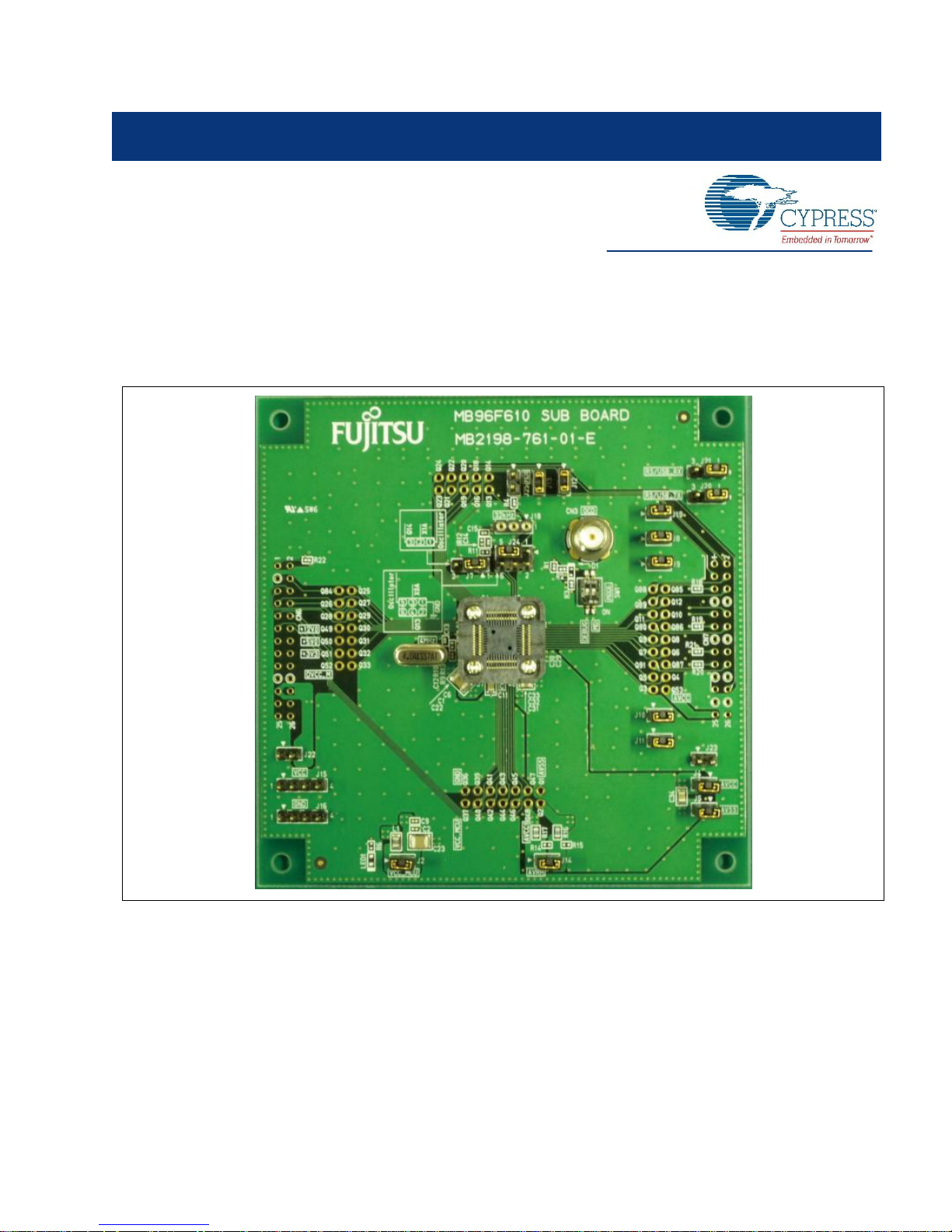
1. Overview
The MB96610 Evaluation Board provides the evaluative environment of the MB96610 series MCU
Figure 1-1. MB96610 Evaluation Board
MB2198-761-01-E/02-E F2MC-16FX Family MB96610 Evaluation Board Operation Guide, Doc. No. 002-05593 Rev. *A 6
Page 7
Overview
monitor
land
Main/Sub
connector
(solder side)
Sub
clock
OCD I/F
RS/USB
selection
monitor
land
Main
clock
MCU
socket
External
Power Supply
connection pin
monitor
land
monitor
land
Mode
SW
Main/Sub
connector
(solder side)
1.1 Functional overview
This board can mount MCU (with or without socket).
The location of the main function is shown as follows.
Figure 1-2. MB96610 Evaluation Board functional overview
MB2198-761-01-E/02-E F2MC-16FX Family MB96610 Evaluation Board Operation Guide, Doc. No. 002-05593 Rev. *A 7
Page 8
Overview
Function
Specification
Remarks
MCU
MB96F610
with socket or direct mounted
with socket
NQPACK048SD-ND
HQPACK048SD
Oscillator
Main clock 4MHz
Sub clock 32.768kHz
with socket
External power supply
connection
External power supply connection
(DC3.3V to 5.0V)
OCD connector
OCD debugger(MB2100-01-E)
Connection
MODE SW
MB96610 mode switch
NMIX SW
MB96610 pin monitor land
RS/USB select
UART ch.0 connect to RS/USB by 3pin Jumper for
transmission and reception.
Main/sub connector
26pins (2 rows × 13 pins) connector × 2
Connect to a connector on the Main board
(mounted solder side)
2.54mm pitch
Table 1-1. MB96610 Evaluation Board function list
MB2198-761-01-E/02-E F2MC-16FX Family MB96610 Evaluation Board Operation Guide, Doc. No. 002-05593 Rev. *A 8
Page 9

Overview
MCU
(MB96610)
With
Socket 48
4MHz
MODE SW
LIN ch.0
USART ch.2
RS ch.0
USB
Main board
DC12V→
·DC5V
·DC3.3V
12V
5.0V
3.3V
OCD connector
CAN ch.0
Monitor LED
INT SW
Monitor
land
32kHz
USART ch.7
CAN ch.2
1.2 Block diagram
The block diagram of this board is shown below.
Figure 1-3. MB96610 Evaluation Board Block Diagram
MB2198-761-01-E/02-E F2MC-16FX Family MB96610 Evaluation Board Operation Guide, Doc. No. 002-05593 Rev. *A 9
Page 10

2. Functional Details
AVRH
AVCC
AVSS
VCC_MCU
The functional details of this board are shown as following.
2.1 Power supply settings
Please confirm the following jumpers are closed.
(J2, J4, J5, J14)
Figure 2-1. Power supply jumpers location
MB2198-761-01-E/02-E F2MC-16FX Family MB96610 Evaluation Board Operation Guide, Doc. No. 002-05593 Rev. *A 10
Page 11

Functional Details
Jumper
Function
Setting
J2
[VCC_MCU]
Power supply for VCC pin
Close (default) : ON
Open : OFF
J14
[AVRH]
Power supply for AVRH pin
Close (default) : ON
Open : OFF
J4
[AVCC]
Power supply for AVCC pin
Close (default) : ON
Open : OFF
J5
[AVSS]
Power supply for AVSS pin
Close (default) : ON
Open : OFF
J7
J24
Table 2-1. Power supply jumpers function
2.2 Sub clock settings
The sub clock connection can be set as follows by J7 and J24.
The settings of these jumpers is shown below.
Note: A sub clock oscillator is not mounted in default. (Xtal 32.768kHz)
Figure 2-2. Sub clock jumpers location
MB2198-761-01-E/02-E F2MC-16FX Family MB96610 Evaluation Board Operation Guide, Doc. No. 002-05593 Rev. *A 11
Page 12

Functional Details
Setting
X1A connection select
1-2
X1A connect to sub clock (default)
2-3
X1A connect to Q14
Setting
X0A connection select
1-3
X0A connect to GND
3-5
X0A connect to sub clock (default)
3-4
X0A connect to Q13
1 2 3
2 4 6 1 3
5
Table 2-2. J7 setting
Table 2-3. J24 setting
MB2198-761-01-E/02-E F2MC-16FX Family MB96610 Evaluation Board Operation Guide, Doc. No. 002-05593 Rev. *A 12
Page 13

Functional Details
Setting
Function select
1-2
RS232C (default)
2-3
USB
J21
J20
From right to left 1, 2, 3
J20:TX , J21:RX
3 2 1
2.3 UART ch.0 select jumper
The connection destination of the UART ch.0 signal can be selected by J20/J21.
These jumpers location and settings are shown below.
Figure 2-3. UART ch.0 select jumper location
Table 2-4. J20, J21 setting
MB2198-761-01-E/02-E F2MC-16FX Family MB96610 Evaluation Board Operation Guide, Doc. No. 002-05593 Rev. *A 13
Page 14

Functional Details
ON
OFF
Mode SW setting
1,2 - MB96610 : serial writer mode
1 2 MB96610 : user mode (default)
Mode SW
bit1:MD , bit2:DEBUG
N
O
1
2
2.4 Mode SW settings
The selection of the operational mode of MCU can be set by SW1 as follows.
The mode switch location and settings are shown below.
Figure 2-4. Mode SW location
MB2198-761-01-E/02-E F2MC-16FX Family MB96610 Evaluation Board Operation Guide, Doc. No. 002-05593 Rev. *A 14
Table 2-5. Mode SW setting (SW1)
Page 15

Functional Details
OCD
connector
Please turn the coaxial cable appended to Cypress
OCD-E(MB21000-01-E) as shown in a left chart.
2.5 OCD (On chip debugger) interface
The MB96610 evaluation board can operate software "Softune" for debugging by connecting Cypress OCD-E (on chip
debugger). The OCD connector location and settings are shown below.
Figure 2-5. OCD cable connect location
MB2198-761-01-E/02-E F2MC-16FX Family MB96610 Evaluation Board Operation Guide, Doc. No. 002-05593 Rev. *A 15
Figure 2-6. How to connect OCD-E
Page 16

Functional Details
Jumper
Signal
J12
LIN I/F ch.0 : RX
J13
LIN I/F ch.0 : TX
J8
RS I/F ch.0 (USB): RX
J9
RS I/F ch.0 (USB): TX
J10
CAN I/F ch.0 : RX
J11
CAN I/F ch.0 : TX
J19
LIN_NSLP0
J2
VCC_MCU : MCU power supply
J4
AVCC : analog power supply
J5
AVSS : analog ground
J14
AVRH : analog reference power supply
2.6 Other jumper settings
These jumpers are in order to free the MCU pin from on board peripherals.
Table 2-6. Isolate jumpers location
MB2198-761-01-E/02-E F2MC-16FX Family MB96610 Evaluation Board Operation Guide, Doc. No. 002-05593 Rev. *A 16
Page 17

Functional Details
Q
Pin No.
Q
Pin No.
Q
Pin No.
2 2 21
21
43
43 3 3
22
22
44
44 4 4
23
23
45
45 5 5
24
24
46
46 6 6
25
25
47
47 7 7
26
26 8 8
27
27 9 9
28
28
10
10
29
29
11
11
30
30
12
12
31
31
13
13
32
32
14
14
33
33
16
16
39
39
18
18
40
40
19
19
41
41
20
20
42
42
2.7 Signal monitor
The correspondence of the monitor land and the MCU pin number is shown as follows. (Q numbers are equal to MCU pin
numbers.)
Table 2-7. Monitor land list
MB2198-761-01-E/02-E F2MC-16FX Family MB96610 Evaluation Board Operation Guide, Doc. No. 002-05593 Rev. *A 17
Page 18

Functional Details
MONITOR LED
Parts number
MB96610
Pin number
Pin name
LED0
LED28
46
P6_0
LED1
LED29
47
P6_1
LED2
LED32
40
P3_0
LED3
LED33
41
P3_1
LED4
LED36
26
P1_4
LED5
LED37
27
P1_5
LED6
LED40
28
P1_6
LED7
LED41
29
P1_7
INT SW
Parts number
MB96610
Pin number
Pin name
INT0
SW4
11
P05_6 (INT4_R)
INT1
SW7
23
P00_3 (INT11)
INT2
SW9
21
P00_4 (INT12)
INT3
SW11
22
P00_5 (INT13)
2.8 Main board connection
The connection of MCU and I/O on the main board is shown below.
General-purpose LED
The correspondence table for the general-purpose LED mounted on the main board and the MCU pin number is shown
below.
Table 2-8. General-purpose LED
Interrupt SW
The correspondence of interruption SW mounted on the main board and the MCU pin number is shown below.
Table 2-9. Interrupt switch
MB2198-761-01-E/02-E F2MC-16FX Family MB96610 Evaluation Board Operation Guide, Doc. No. 002-05593 Rev. *A 18
Page 19

Functional Details
NMI SW
Parts number
MB96610
Pin number
Pin name
NMI
SW3
12
NMI
Reset SW
Parts number
MB96610
Pin number
Pin name
RESET
SW2
33
RSTX
Volume SW
Parts number
MB96610
Pin number
Pin name
Volume
VR1 3 P06_3 (AN3)
NMI SW
The correspondence of NMI SW mounted on the main board and the MCU pin number is shown below.
Table 2-10. NMI switch
Reset SW
The correspondence of RESET SW mounted on the main board and the MCU pin number is shown below.
Table 2-11. RESET switch
Volume SW
The correspondence of Volume SW mounted on the main board and the MCU pin number is shown below.
Table 2-12. Volume switch
MB2198-761-01-E/02-E F2MC-16FX Family MB96610 Evaluation Board Operation Guide, Doc. No. 002-05593 Rev. *A 19
Page 20

3. Power-ON
GND
VCC
Basically, this board cannot turn on the power supply alone.
Please mount on the main board(MB2198-760-E) and use it.
3.1 FOR TEST USE ONLY, External power supply connection pin
The external power supply connection position is shown as follows.
(VCC = 3.3V to 5.0V)
When you connect an external power supply to this pin, and you use alone this board, please short-circuit J22 (DVCC)
and J23 (AVCC).
Figure 3-1. External power supply connection pin location
3.2 Power-ON
Please follow the user's manual for the Main board(MB2198-760-E).
MB2198-761-01-E/02-E F2MC-16FX Family MB96610 Evaluation Board Operation Guide, Doc. No. 002-05593 Rev. *A 20
Page 21

4. Circuit Diagram
J20 WL-1-3P
123
R4
1005 10kΩ 5%
12
Q89Q
C23
3225 10µF 25V
12
Q32Q
J12WL-1-2P
1 2
Q16Q
J24
WLW-1-3PW
1 2
3 4
5 6
Q46Q
Q53Q
Q20Q
Q44Q
Q28Q
R1
1005 10kΩ 5%
12
Q2Q
Q37Q
J14 WL-1-2P12R16
1608 10Ω 1%
1 2
CN3
HRM-300-134B(40)
1
2
3
4
5
Q23Q
R13 1005 10kΩ 5%
1 2
Q88Q
Q41Q
Q90Q
C33
1005 220pF 25V
12
C22
3225 10µF 25V
12
Q49Q
CN7
HIF3FB-26DA-2.54DSA(71)
13579
11
13
15
1719212325
246810
12
14
16
1820222426
J19WL-1-2P
1 2
Q30Q
J13WL-1-2P
1 2
C32
1005 0.1µF 25V
12
L1
BLM21PG600SN1
1 2
Q29Q
Q11Q
C12
1005 10pF 50V
1 2
Q43Q
Q13Q
R15
1005 1MΩ 5%
12
Q21Q
C31
2012 1µF 16V
12
Q47Q
Q91Q
J21 WL-1-3P
123
Q6Q
C9
1005 0.01µF 25V
12
Q4Q
R10
1005 0Ω
1 2
R22
1005 10kΩ 5%
1 2
CN6
HIF3FB-26DA-2.54DSA(71)
13579
11
13
1517192123
25
246
8
10
12
14
1618202224
26
R2
1005 43Ω 5%
1 2
Q26Q
R17
1608 4.7Ω 1%
1 2
Q45Q
J9WL-1-2P
1 2
J17
PM-1-3P
123
Q42Q
Q33Q
J16
WL-1-4P
1
2
3
4
Q85Q
Q9Q
Q7Q
J5
WL-1-2P
1 2
Q40Q
Q50Q
Q19Q
C2
1005 0.1µF 25V
12
C11
2012 4.7µF 16V
12
C1
1005 0.1µF 25V
12
R6
1005 470Ω
1 2
Q31Q
C14
1005 10pF 50V
1 2
R11
1005 1MΩ 5%
12
R19
1 2
Q39Q
Q12Q
Q8Q
SW1
CHS-02B
1
2 3
4
R3
1005 10kΩ 5%
12
Q84Q
J4
WL-1-2P
1 2
C29
1005 0.1µF 25V
12
D1
RN262GT2R
1 2
KA
R12
1005 0Ω
1 2
J22 WL-1-2P
1 2
Q22Q
C13
1005 10pF 50V
1 2
J7
WL-1-3P
123
J10WL-1-2P
1 2
U1 NQPACK048SD(MB96F610)
123
4
5
6
78910111213
14
15
1617181920212223242526272829303132
33
34
35
3637383940
41
43
44
4546474248
LQFP-48
Package code (mold)
FPT-48P-M26
Q52Q
Q36Q
Q14Q
Q51Q
Q86Q
C30
1005 22pF 25V
12
Q1Q
Q27Q
R18
1 2
J23 WL-1-2P
1 2
R21
1 2
Q3Q
Q24Q
R9
1005 1MΩ 5%
12
C34
2012 1µF 16V
12
C15
1005 10pF 50V
1 2
Q10Q
J2
WL-1-2P
1 2
J11WL-1-2P
1 2
J18
PM-1-3P
123
J15
WL-1-4P
1
2
3
4
J8WL-1-2P
1 2
J25
WL-1-2P
1 2
LED1
CL-190G
1 2
Q5Q
Q18Q
R14
1005 1MΩ 5%
12
Q25Q
Q87Q
R20
1005 10kΩ 5%
1 2
C6
1005 0.01µF 25V
12
Q48Q
C
P05_4
DEBUG_IF
P00_0
P00_4
P00_5
P00_3
P01_0
P01_1
P01_4
P01_5
P02_0
P02_2
P02_4
RSTX
X1
X0
P02_5
P03_1
P03_2
P03_6
P06_6
P06_7
P05_0
P05_1
P05_2
P05_6
P07_0
X0A
X1A
MD
P03_3
P03_7
P06_0
P06_1
P03_2P03_3
P00_1
P00_0
P00_2
P07_0 RSTX
P06_1
P03_1
P01_5
P01_7
P00_3
P00_5
P06_3
P05_6
P00_4
P06_0
P03_0
P01_4
P01_6
X0
X1
P04_1
X1A
C
DEBUG_IF
P06_4
P06_3
P01_6
P01_7
AVRH
P05_1
P05_0
X0A P04_0
P17_0
P00_1
P00_2
P03_0
MD
P17_0
DGND
AVRH
AVCC1
AVSS
DGND
VCC
DGND
DGND
AVCC1
AVSS
VCC_MCU
DGND
VCC_MCU
AVCC1AVCC
VCC
DGND
VCC_MCU
DGND DGND
DGND DGND
DGND
DGND
VCC
AVSS
DGND
AVRH
VCC
DGND
VCC
VCC
AVCC
DVCC_M
DGND
+5V0
+3V3
+12V0
DVCC_M
VCC
AVCC
DGND
VCC_MCU
VCC
OCD
4MHz
MB96F610 MODE SET/OCD IF
MB96F610 MainCLK IF
MB96F610 SubCLK IF
32kHz
MB96F610 Monitor pin
(Qxx-Qyy = 2.54mm pitch)
Power Div IF
Main/Sub CN
Non-Mount
(P04_0/X0A)
(P04_1/X1A)
Non-Mount
C
MB96F610 C-pin
MODE
MD
(LIN_TX0)
(LIN_NSLP0)
(LIN_TX1)
(CAN_TX0)
(NMI_SW)
(RS_TX0)
(RS_TX1)
(RS_RX0)
(RS_RX1)
(LIN_RX0)
(LIN_NSLP1)
(LIN_RX1)
(CAN_RX0)
(CAN_RX1)
(RESET)
(Volume_SW)
(INT_SW1)
(INT_SW3)
(LED1)
(LED3)
(LED5)
(LED7)
(LED0)
(USB_TX0)(USB_RX0)
(LED2)
(LED6)
(LED4)
(INT_SW0)
(INT_SW2)
Non-MountNon-Mount
(CAN_TX1)
DT-38_32.768kHz_SK
HC49SFWB_4MHz_SK
VCC GND
Non-Mount
[R18-R21]
RS/USB_TX
RS/USB_RX
Stand-alone J22-J23 short
48pin socket type : NQPACK048SD
(Socket Head : HQPACK048SD)
(RS:1pin-2pin short)
(USB:2pin-3pin short)
(RS:1pin-2pin short)
(USB:2pin-3pin short)
(CN6-23,25,26pin)
(CN7-25,26pin)
+3V3
+5V0
DVCC_M
+12V0
X0A
GND
Q13
Oscillator
AVCC
VCC_MCU
VCC_MCU
GND
AVCC
AVSS
AVRH
AVCC1
AVSS
Oscillator
Q14
X1A
DEBUG
MD1
AVSS
AVRH
P06_3/AN3/PPG3
P06_4/AN4/PPG4
P06_6/AN6/PPG6
P06_7/AN7/PPG7
P05_0/AN8/SIN2/INT3_R1
P05_1/AN9/SOT2
P05_2/AN10/SCK2
P05_4/AN12/TOT3/INT2_R
P05_6/AN14/INT4_R
P07_0/AN16/INT0/NMI
P04_0/X0A
P04_1/X1A
MD
P17_0
DEBUG I/F
P00_0/INT8/SCK7_R/PPG0_B
P00_1/INT9/SOT7_R/PPG1_B
P00_2/INT10/SIN7_R
P00_4/INT12/SOT8_R/PPG12_B
P00_5/INT13/SIN8_R/PPG14_B
P00_3/INT11/SCK8_R/PPG3_B
P01_0/TIN1/CKOT1/OUT0_R
P01_1/TOT1/CKOTX1/OUT1_R
P01_4/PPG4_B
P01_5/SIN2_R/INT7_R
P01_6/SOT2_R/PPG6_B
P01_7/SCK2_R/PPG7_B
P02_0/PPG12/CKOT1_R
P02_2/ZIN0/PPG14/CKOT0_R
P02_4/AIN0/IN0/TTG0
RSTX
X1
X0
VSS
VCC
C
P02_5/BIN0/IN1/TTG1/ADTG_R
P03_0/AIN1/IN4/TTG4/AN24/TTG12
P03_1/BIN1/TTG5/TTG13/IN5/AN25
P03_3/TX2
P03_6/ZIN1/OUT6/AN30
P03_7/OUT7/AN31
P06_0/AN0/PPG0
P06_1/AN1/PPG1
P03_2/INT10_R/RX2
AVCC
1 2
3 4
5 6
1
2
3
MB2198-761-01-E/02-E F2MC-16FX Family MB96610 Evaluation Board Operation Guide, Doc. No. 002-05593 Rev. *A 21
Page 22

5. Recycling
Valid for European Union Countries:
According to the European WEEE-Directive and its implementation into national laws we take this device back.
For disposal please send the device to the following address:
Cypress Semiconductor
198 Champion Court
San Jose, CA 95134-1709
Gültig für EU-Länder:
Gemäß der Europäischen WEEE-Richtlinie und deren Umsetzung in landesspezifische
Gesetze nehmen wir dieses Gerät wieder zurück.
Zur Entsorgung schicken Sie das Gerät bitte an die folgende Adresse:
Cypress Semiconductor
198 Champion Court
San Jose, CA 95134-1709
MB2198-761-01-E/02-E F2MC-16FX Family MB96610 Evaluation Board Operation Guide, Doc. No. 002-05593 Rev. *A 22
Page 23

6. China-RoHS Regulation
这标记是按照2006年2月28日公布的[电子信息产品污染控制管理办法]以及SJ/T11364-2006[电子信息产品
污染控制标识要求]在中国销售的电子信息产品的环保使用期限。如遵守关于这产品的安全或使用上的注意
,在这期限内(从生产日期起算)不会因产品中的有害物质漏到外部、或发生突然变异,而引起环境污染和对
人体或财产的重大影响。
部件名称
有毒有害物质或元素
铅
(Pb) 汞 (Hg) 镉 (Cd)
六价铬
(Cr(VI))
多溴联苯
(PBB)
多溴二苯醚
(PBDE)
印刷线路板
× ○ ○ ○ ○
○
电源
○ ○ ○ ○ ○
○
○:表示该有毒有害物质在该部件所有均质材料中的含量均在SJ/T 11363-2006规定的限量要求以下。
×:表示该有毒有害物质至少在该部件的某一均质材料中的含量超出SJ/T 11363-2006 规定的限量要求。
Compliance with Administration on the Control of Pollution Caused by Electronic Information Products of the People’s
Republic of China
产品中有毒有害物质或元素的名称及含量
MB2198-761-01-E/02-E F2MC-16FX Family MB96610 Evaluation Board Operation Guide, Doc. No. 002-05593 Rev. *A 23
Page 24

Revision History
Document Title: MB2198-761-01-E/02-E F2MC-16FX Family MB96610 Evaluation Board Operation Guide
Document Number: 002-05593
Revision
Issue Date
Origin of
Change
Description of Change
**
07/19/2012
MITK
Initial release
*A
04/29/2016
MITK
Migrated Spansion Guide from SS704-00001-1v0-E to Cypress format
Document Revision History
MB2198-761-01-E/02-E F2MC-16FX Family MB96610 Evaluation Board Operation Guide, Doc. No. 002-05593 Rev. *A 24
 Loading...