

Page 1

Ultra37000 CPLD Family
5V, 3.3V, ISR™ High-Performance CPLDs
Features
• In-System Reprogrammable™ (ISR™) CMOS CPLDs
— JTAG interface for reconfigurability
— Design changes do not cause pinout changes
— Design changes do not cause timing changes
• High density
— 32 to 512 macrocells
— 32 to 264 I/O pins
— Five dedicated inputs including four clock pins
• Simple timing model
— No fanout delays
— No expander delays
— No dedicated vs. I/O pin delays
— No additional delay through PIM
— No penalty for using full 16 product terms
— No delay for steering or sharing product terms
• 3.3V and 5V versions
• PCI-compatible
• Programmable bus-hold capabilities on all I/Os
• Intelligent product term allocator provides:
— 0 to 16 product terms to any macrocell
— Product term steering on an individual basis
— Product term sharing among local macrocells
• Flexible clocking
— Four synchronous clocks per device
— Product term clocking
— Clock polarity control per logic block
• Consistent package/pinout offering across all densities
— Simplifies design migration
— Same pinout for 3.3V and 5.0V devices
• Packages
— 44 to 400 leads in PLCC, CLCC, PQFP, TQFP, CQFP,
BGA, and Fine-Pitch BGA packages
— Lead (Pb)-free packages available
Note:
1. Due to the 5V-tolerant nature of 3.3V device I/Os, the I/Os are not clamped to V
[1]
General Description
The Ultra37000™ family of CMOS CPLDs provides a range of
high-density programmable logic solutions with unparalleled
system performance. The Ultra37000 family is designed to
bring the flexibility, ease of use, and performance of the 22V10
to high-density CPLDs. The architecture is based on a number
of logic blocks that are connected by a Programmable Interconnect Matrix (PIM). Each logic block features its own
product term array, product term allocator, and 16 macrocells.
The PIM distributes signals from the logic block outputs and all
input pins to the logic block inputs.
All of the Ultra37000 devices are electrically erasable and
In-System Reprogrammable (ISR), which simplifies both
design and manufacturing flows, thereby reducing costs. The
ISR feature provides the ability to reconfigure the devices
without having design changes cause pinout or timing
changes. The Cypress ISR function is implemented through a
JTAG-compliant serial interface. Data is shifted in and out
through the TDI and TDO pins, respectively. Because of the
superior routability and simple timing model of the Ultra37000
devices, ISR allows users to change existing logic designs
while simultaneously fixing pinout assignments and
maintaining system performance.
The entire family features JTAG for ISR and boundary scan,
and is compatible with the PCI Local Bus specification,
meeting the electrical and timing requirements. The
Ultra37000 family features user programmable bus-hold
capabilities on all I/Os.
Ultra37000 5.0V Devices
The Ultra37000 devices operate with a 5V supply and can
support 5V or 3.3V I/O levels. V
capability of interfacing to either a 5V or 3.3V bus. By
connecting the V
on the outputs. If V
meet 3.3V JEDEC standard CMOS levels and are 5V tolerant.
pins to 5V the user insures 5V TTL levels
CCO
is connected to 3.3V the output levels
CCO
These devices require 5V ISR programming.
Ultra37000V 3.3V Devices
Devices operating with a 3.3V supply require 3.3V on all V
pins, reducing the device’s power consumption. These
devices support 3.3V JEDEC standard CMOS output levels,
and are 5V-tolerant. These devices allow 3.3V ISR
programming.
, PCI V
CC
IH
= 2V.
connections provide the
CCO
CCO
Cypress Semiconductor Corporation • 3901 North First Street • San Jose, CA 95134 • 408-943-2600
Document #: 38-03007 Rev. *E Revised March 7, 2004
[+] Feedback
Page 2
Ultra37000 CPLD Family
Selection Guide
5.0V Selection Guide
General Information
Device Macrocells Dedicated Inputs I/O Pins Speed (t
CY37032 32 5 32 6 200
CY37064 64 5 32/64 6 200
CY37128 128 5 64/128 6.5 167
CY37192 192 5 120 7.5 154
CY37256 256 5 128/160/192 7.5 154
CY37384 384 5 160/192 10 118
CY37512 512 5 160/192/264 10 118
Speed Bins
Device 200 167 154 143 125 100 83 66
CY37032 X X X
CY37064 X X X
CY37128 X X X
CY37192 X X X
CY37256 X X X
CY37384 X X
CY37512 X X X
)Speed (f
PD
MAX
)
Device-Package Offering and I/O Count
Device
44-
Lead
TQFP
44-
Lead
PLCC
44-
Lead
CLCC
84-
Lead
PLCC
84-
Lead
CLCC
100-
Lead
TQFP
160-
Lead
TQFP
160-
Lead
CQFP
208-
Lead
PQFP
208-
Lead
CQFP
292-
Lead
PBGA
CY37032 37 37
CY37064 37 37 37 69 69
CY37128 69 69 69 133
CY37192 125
CY37256 133 133 165 197
CY37384 165 197
CY37512 165 165 197 269
3.3V Selection Guide
General Information
Device Macrocells Dedicated Inputs I/O Pins Speed (t
)Speed (f
PD
CY37032V 32 5 32 8.5 143
CY37064V 64 5 32/64 8.5 143
CY37128V 128 5 64/80/128 10 125
CY37192V 192 5 120 12 100
CY37256V 256 5 128/160/192 12 100
CY37384V 384 5 160/192 15 83
CY37512V 512 5 160/192/264 15 83
388-
Lead
PBGA
MAX
)
Document #: 38-03007 Rev. *E Page 2 of 64
[+] Feedback
Page 3
Ultra37000 CPLD Family
Speed Bins
Device 200 167 154 143 125 100 83 66
CY37032V X X
CY37064V X X
CY37128V X X
CY37192V XX
CY37256V XX
CY37384V XX
CY37512V XX
Device-Package Offering and I/O Count
Device
44-
44-
Lead
TQFP
48-
Lead
CLCC
84-
Lead
FBGA
100-
Lead
CLCC
100-
Lead
TQFP
160-
Lead
FBGA
160-
Lead
TQFP
208-
Lead
CQFP
Lead
208-
PQFP
292-
Lead
CQFP
Lead
256-
PBGA
388-
Lead
Lead
FBGA
PBGA
CY37032V 37 37
CY37064V 37 37 37 69 69
CY37128V 69 69 85 133
CY37192V 125
CY37256V 133 133 165 197 197
CY37384V 165 197
CY37512V 165 165 197 269 269
Architecture Overview of Ultra37000 Family
Programmable Interconnect Matrix
The PIM consists of a completely global routing matrix for
signals from I/O pins and feedbacks from the logic blocks. The
PIM provides extremely robust interconnection to avoid fitting
and density limitations.
The inputs to the PIM consist of all I/O and dedicated input pins
and all macrocell feedbacks from within the logic blocks. The
number of PIM inputs increases with pin count and the number
of logic blocks. The outputs from the PIM are signals routed to
the appropriate logic blocks. Each logic block receives 36
inputs from the PIM and their complements, allowing for 32-bit
operations to be implemented in a single pass through the
device. The wide number of inputs to the logic block also
improves the routing capacity of the Ultra37000 family.
An important feature of the PIM is its simple timing. The propagation delay through the PIM is accounted for in the timing
specifications for each device. There is no additional delay for
traveling through the PIM. In fact, all inputs travel through the
PIM. As a result, there are no route-dependent timing parameters on the Ultra37000 devices. The worst-case PIM delays
are incorporated in all appropriate Ultra37000 specifications.
Routing signals through the PIM is completely invisible to the
user. All routing is accomplished by software—no hand routing
is necessary. Warp
automatically route designs for the Ultra37000 family in a
matter of minutes. Finally, the rich routing resources of the
Ultra37000 family accommodate last minute logic changes
while maintaining fixed pin assignments.
®
and third-party development packages
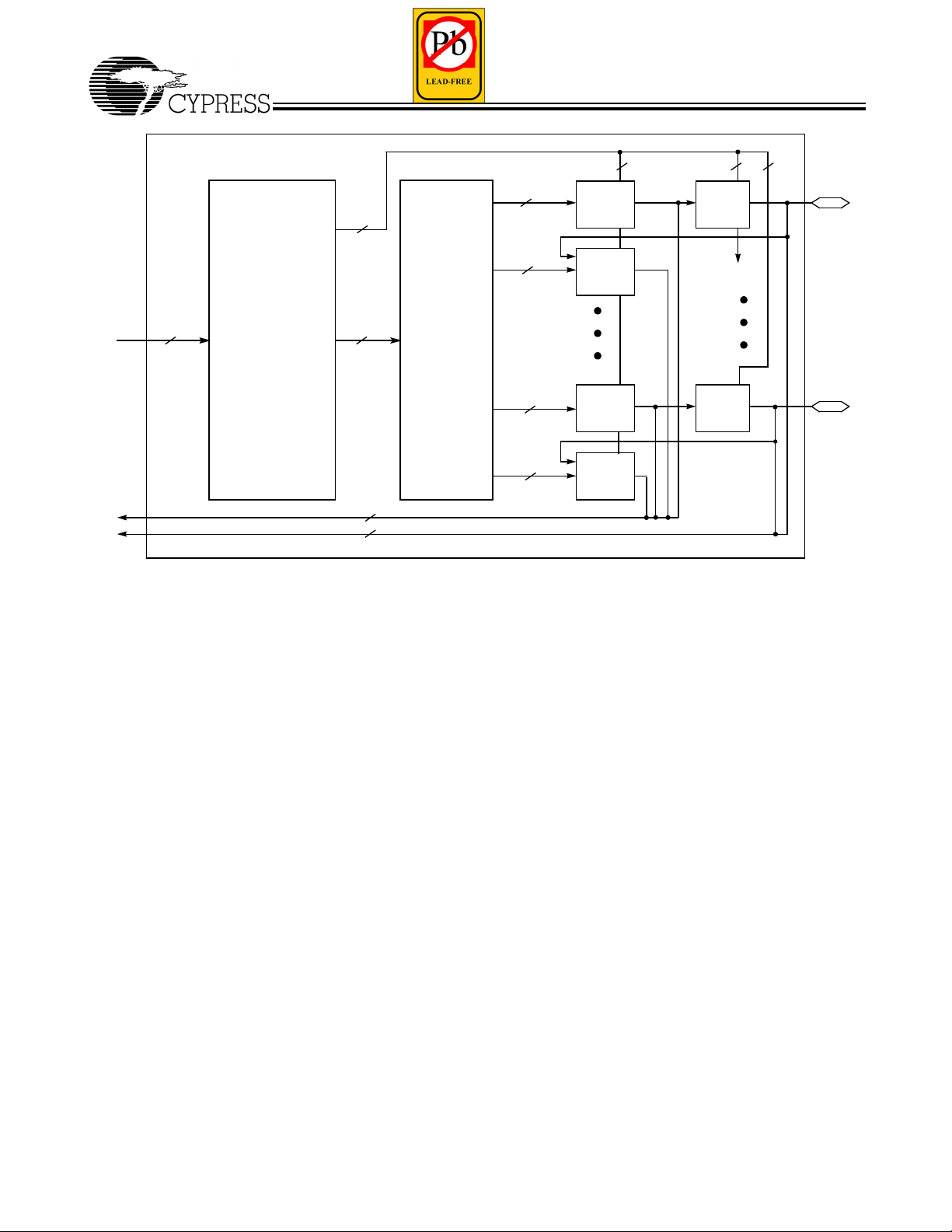
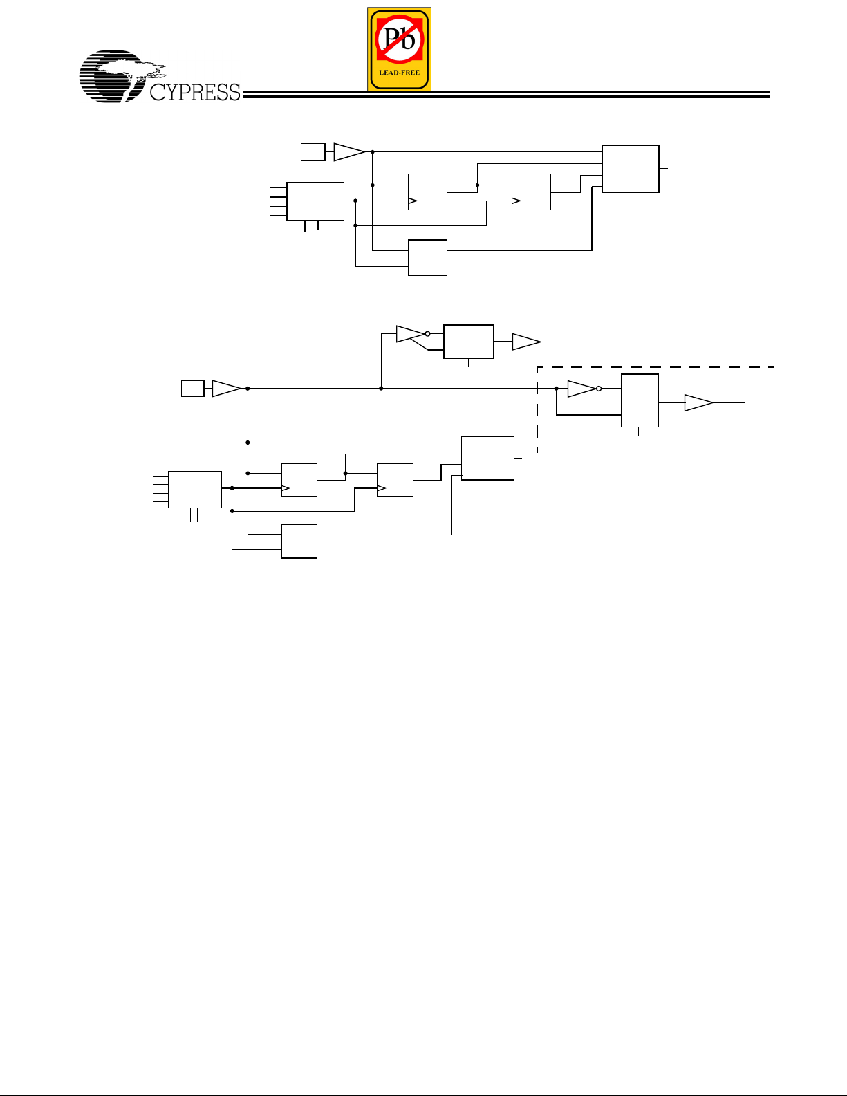
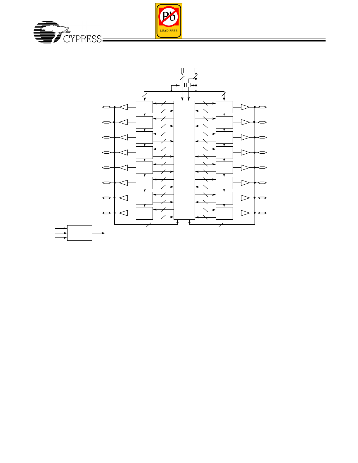
Logic Block
The logic block is the basic building block of the Ultra37000
architecture. It consists of a product term array, an intelligent
product-term allocator, 16 macrocells, and a number of I/O
cells. The number of I/O cells varies depending on the device
used. Refer to Figure 1 for the block diagram.
Product Term Array
Each logic block features a 72 x 87 programmable product
term array. This array accepts 36 inputs from the PIM, which
originate from macrocell feedbacks and device pins. Active
LOW and active HIGH versions of each of these inputs are
generated to create the full 72-input field. The 87 product
terms in the array can be created from any of the 72 inputs.
Of the 87 product terms, 80 are for general-purpose use for
the 16 macrocells in the logic block. Four of the remaining
seven product terms in the logic block are output enable (OE)
product terms. Each of the OE product terms controls up to
eight of the 16 macrocells and is selectable on an individual
macrocell basis. In other words, each I/O cell can select
between one of two OE product terms to control the output
buffer. The first two of these four OE product terms are
available to the upper half of the I/O macrocells in a logic block.
The other two OE product terms are available to the lower half
of the I/O macrocells in a logic block.
The next two product terms in each logic block are dedicated
asynchronous set and asynchronous reset product terms. The
final product term is the product term clock. The set, reset, OE
and product term clock have polarity control to realize OR
functions in a single pass through the array.
400-
Lead
FBGA
Document #: 38-03007 Rev. *E Page 3 of 64
[+] Feedback
Page 4
FROM
PIM
72 x 87
PRODUCT TERM
ARRAY
Ultra37000 CPLD Family
2
3
0−16
PRODUCT
TERMS
7
8036
PRODUCT
TERM
ALLOCATOR
0−16
PRODUCT
TERMS
MACRO-
CELL
0
MACRO-
CELL
1
I/O
CELL
0
to cells
2
2, 4, 6 8, 10, 12
TO
PIM
16
8
Figure 1. Logic Block with 50% Buried Macrocells
Low-Power Option
Each logic block can operate in high-speed mode for critical
path performance, or in low-power mode for power conservation. The logic block mode is set by the user on a logic block
by logic block basis.
Product Term Allocator
Through the product term allocator, software automatically
distributes product terms among the 16 macrocells in the logic
block as needed. A total of 80 product terms are available from
the local product term array. The product term allocator
provides two important capabilities without affecting performance: product term steering and product term sharing.
Product Term Steering
Product term steering is the process of assigning product
terms to macrocells as needed. For example, if one macrocell
requires ten product terms while another needs just three, the
product term allocator will “steer” ten product terms to one
macrocell and three to the other. On Ultra37000 devices,
product terms are steered on an individual basis. Any number
between 0 and 16 product terms can be steered to any
macrocell. Note that 0 product terms is useful in cases where
a particular macrocell is unused or used as an input register.
Product Term Sharing
Product term sharing is the process of using the same product
term among multiple macrocells. For example, if more than
one output has one or more product terms in its equation that
are common to other outputs, those product terms are only
programmed once. The Ultra37000 product term allocator
allows sharing across groups of four output macrocells in a
0−16
PRODUCT
TERMS
0−16
PRODUCT
TERMS
MACRO-
CELL
14
MACRO-
CELL
15
I/O
CELL
14
variable fashion. The software automatically takes advantage
of this capability—the user does not have to intervene.
Note that neither product term sharing nor product term
steering have any effect on the speed of the product. All
worst-case steering and sharing configurations have been
incorporated in the timing specifications for the Ultra37000
devices.
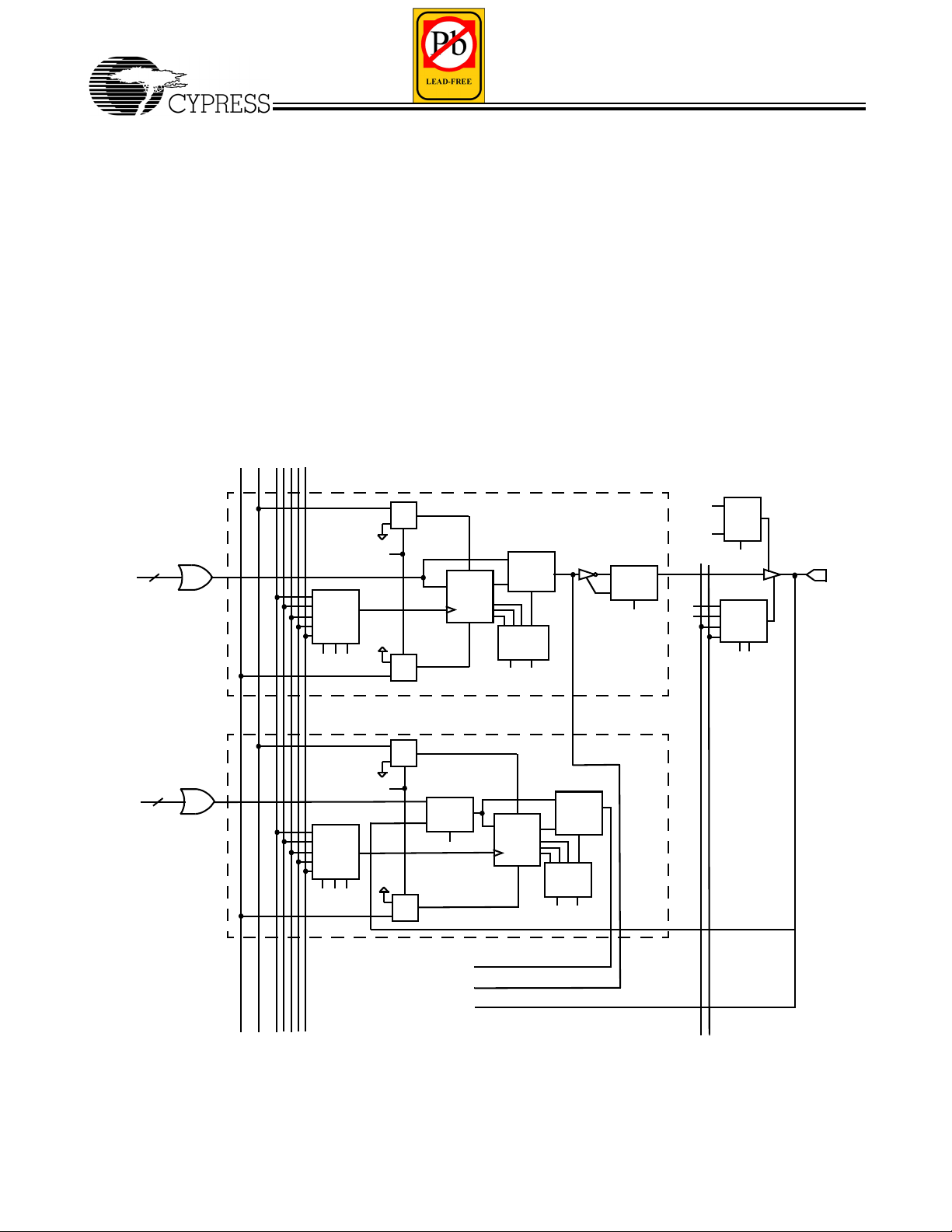
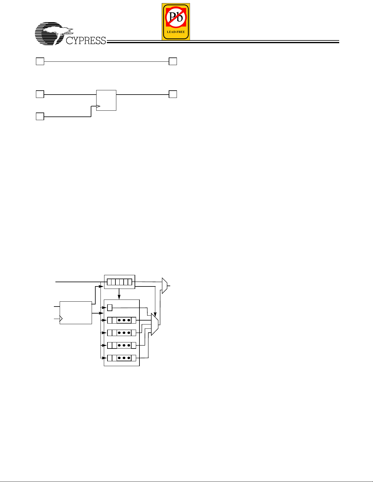
Ultra37000 Macrocell
Within each logic block there are 16 macrocells. Macrocells
can either be I/O Macrocells, which include an I/O Cell which
is associated with an I/O pin, or buried Macrocells, which do
not connect to an I/O. The combination of I/O Macrocells and
buried Macrocells varies from device to device.
Buried Macrocell
Figure 2 displays the architecture of buried macrocells. The
buried macrocell features a register that can be configured as
combinatorial, a D flip-flop, a T flip-flop, or a level-triggered
latch.
The register can be asynchronously set or asynchronously
reset at the logic block level with the separate set and reset
product terms. Each of these product terms features programmable polarity. This allows the registers to be set or reset
based on an AND expression or an OR expression.
Clocking of the register is very flexible. Four global
synchronous clocks and a product term clock are available to
clock the register. Furthermore, each clock features programmable polarity so that registers can be triggered on falling as
well as rising edges (see the Clocking section). Clock polarity
is chosen at the logic block level.
Document #: 38-03007 Rev. *E Page 4 of 64
[+] Feedback
Page 5
Ultra37000 CPLD Family
The buried macrocell also supports input register capability.
The buried macrocell can be configured to act as an input
register (D-type or latch) whose input comes from the I/O pin
associated with the neighboring macrocell. The output of all
buried macrocells is sent directly to the PIM regardless of its
configuration.
I/O Macrocell
Figure 2 illustrates the architecture of the I/O macrocell. The
I/O macrocell supports the same functions as the buried
macrocell with the addition of I/O capability. At the output of the
macrocell, a polarity control mux is available to select active
LOW or active HIGH signals. This has the added advantage
of allowing significant logic reduction to occur in many applications.
The Ultra37000 macrocell features a feedback path to the PIM
separate from the I/O pin input path. This means that if the
macrocell is buried (fed back internally only), the associated
I/O pin can still be used as an input.
I/O MACROCELL
FROM PTM
0−16
PRODUCT
TERMS
0
1
2
3
4
C24
C0
C1
0
1
C25
D/T/L
O
1
0
Bus Hold Capabilities on all I/Os
Bus-hold, which is an improved version of the popular internal
pull-up resistor, is a weak latch connected to the pin that does
not degrade the device’s performance. As a latch, bus-hold
maintains the last state of a pin when the pin is placed in a
high-impedance state, thus reducing system noise in
bus-interface applications. Bus-hold additionally allows
unused device pins to remain unconnected on the board,
which is particularly useful during prototyping as designers can
route new signals to the device without cutting trace connections to V
note Understanding Bus-Hold—A Feature of Cypress CPLDs.
or GND. For more information, see the application
CC
Programmable Slew Rate Control
Each output has a programmable configuration bit, which sets
the output slew rate to fast or slow. For designs concerned with
meeting FCC emissions standards the slow edge provides for
lower system noise. For designs requiring very high performance the fast edge rate provides maximum system performance.
FAST
SLEW
SLOW
0
1
DECODE
C2 C3
O
P
Q
R
O
0
1
C4
“0”
“1”
C26
0
1
2
3
C6 C5
I/O CELL
O
BURIED MACROCELL
FROM PTM
0−16
PRODUCT
TERMS
ASYNCHRONOUS
BLOCK RESET
ASYNCHRONOUS
BLOCK PRESET
0
1
2
3
4
C24
C0
C1
4 SYNCHRONOUS CLOCKS (CLK0,CLK1,CLK2,CLK3)
1 ASYNCHRONOUS CLOCK(PTCLK)
0
1
C25
0
O
1
Q
1
0
C7
D/T/L Q
FEEDBACK TO PIM
FEEDBACK TO PIM
FEEDBACK TO PIM
0
1
DECODE
C2 C3
O
OE0
OE1
P
R
Figure 2. I/O and Buried Macrocells
Document #: 38-03007 Rev. *E Page 5 of 64
[+] Feedback
Page 6
FROM CLOCK
POLARITY MUXES
0
1
2
3
C10
INPUT PIN
O
C11
D
Q
D
Q
LE
Figure 3. Input Macrocell
Ultra37000 CPLD Family
0
1
O
D
Q
2
3
C12 C13
TO PIM
INPUT/CLOCK PIN
FROM CLOCK
POLARITY INPUT
CLOCK PINS
0
1
O
2
3
C8
C9
D
Q
D
Q
LE
D
Figure 4. Input/Clock Macrocell
Clocking
Each I/O and buried macrocell has access to four synchronous
clocks (CLK0, CLK1, CLK2 and CLK3) as well as an
asynchronous product term clock PTCLK. Each input
macrocell has access to all four synchronous clocks.
Dedicated Inputs/Clocks
Five pins on each member of the Ultra37000 family are designated as input-only. There are two types of dedicated inputs
on Ultra37000 devices: input pins and input/clock pins.
Figure 3 illustrates the architecture for input pins. Four input
options are available for the user: combinatorial, registered,
double-registered, or latched. If a registered or latched option
is selected, any one of the input clocks can be selected for
control.
Figure 4 illustrates the architecture for the input/clock pins.
Like the input pins, input/clock pins can be combinatorial,
registered, double-registered, or latched. In addition, these
pins feed the clocking structures throughout the device. The
clock path at the input has user-configurable polarity.
Product Term Clocking
In addition to the four synchronous clocks, the Ultra37000
family also has a product term clock for asynchronous
clocking. Each logic block has an independent product term
clock which is available to all 16 macrocells. Each product term
clock also supports user configurable polarity selection.
0
O
1
C12
0
1
O
2
Q
3
C10C11
TO CLOCK MUX ON
ALL INPUT MACROCELLS
TO PIM
0
O
1
C13, C14, C15 OR C16
CLOCK POLARITY MUX
ONE PER LOGIC BLOCK
FOR EACH CLOCK INPUT
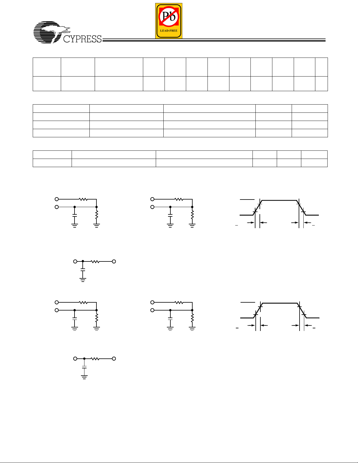
Timing Model
One of the most important features of the Ultra37000 family is
the simplicity of its timing. All delays are worst case and
system performance is unaffected by the features used.
Figure 5 illustrates the true timing model for the 167-MHz
devices in high speed mode. For combinatorial paths, any
input to any output incurs a 6.5-ns worst-case delay regardless
of the amount of logic used. For synchronous systems, the
input set-up time to the output macrocells for any input is 3.5
ns and the clock to output time is also 4.0 ns. These measurements are for any output and synchronous clock, regardless
of the logic used.
The Ultra37000 features:
• No fanout delays
• No expander delays
• No dedicated vs. I/O pin delays
• No additional delay through PIM
• No penalty for using 0–16 product terms
• No added delay for steering product terms
• No added delay for sharing product terms
• No routing delays
• No output bypass delays
The simple timing model of the Ultra37000 family eliminates
unexpected performance penalties.
TO CLOCK MUX
IN EACH
LOGIC BLOCK
Document #: 38-03007 Rev. *E Page 6 of 64
[+] Feedback
Page 7
Ultra37000 CPLD Family
COMBINATORIAL SIGNAL
t
= 6.5 ns
INPUT
tS = 3.5 ns
INPUT
CLOCK
PD
REGISTERED SIGNAL
D,T,L O
t
CO
OUTPUT
= 4.5 ns
OUTPUT
Figure 5. Timing Model for CY37128
JTAG and PCI Standards
PCI Compliance
5V operation of the Ultra37000 is fully compliant with the PCI
Local Bus Specification published by the PCI Special Interest
Group. The 3.3V products meet all PCI requirements except
for the output 3.3V clamp, which is in direct conflict with 5V
tolerance. The Ultra37000 family’s simple and predictable
timing model ensures compliance with the PCI AC specifications independent of the design.
IEEE 1149.1-compliant JTAG
The Ultra37000 family has an IEEE 1149.1 JTAG interface for
both Boundary Scan and ISR.
Boundary Scan
The Ultra37000 family supports Bypass, Sample/Preload,
Extest, Idcode, and Usercode boundary scan instructions. The
JTAG interface is shown in Figure 6.
Instruction Register
TDI
TMS
TCK
JTAG
TAP
CONTROLLER
Bypass Reg.
Boundary Scan
idcode
Usercode
ISR Prog.
Data Registers
Figure 6. JTAG Interface
In-System Reprogramming (ISR)
In-System Reprogramming is the combination of the capability
to program or reprogram a device on-board, and the ability to
support design changes without changing the system timing
or device pinout. This combination means design changes
during debug or field upgrades do not cause board respins.
The Ultra37000 family implements ISR by providing a JTAG
compliant interface for on-board programming, robust routing
TDO
resources for pinout flexibility, and a simple timing model for
consistent system performance.
Development Software Support
Warp
Warp is a state-of-the-art compiler and complete CPLD design
tool. For design entry, Warp provides an IEEE-STD-1076/1164
VHDL text editor, an IEEE-STD-1364 Verilog text editor, and a
graphical finite state machine editor. It provides optimized
synthesis and fitting by replacing basic circuits with ones
pre-optimized for the target device, by implementing logic in
unused memory and by perfect communication between fitting
and synthesis. To facilitate design and debugging, Warp
provides graphical timing simulation and analysis.
Warp Professional
Warp Professional contains several additional features. It
provides an extra method of design entry with its graphical
block diagram editor. It allows up to 5 ms timing simulation
instead of only 2 ms. It allows comparison of waveforms before
and after design changes.
Warp Enterprise
Warp Enterprise provides even more features. It provides
unlimited timing simulation and source-level behavioral
simulation as well as a debugger. It has the ability to generate
graphical HDL blocks from HDL text. It can even generate
testbenches.
Warp is available for PC and UNIX platforms. Some features
are not available in the UNIX version. For further information
see the Warp for PC, Warp for UNIX, Warp Professional and
Warp Enterprise data sheets on Cypress’s web site
(www.cypress.com).
Third-Party Software
Although Warp is a complete CPLD development tool on its
own, it interfaces with nearly every third party EDA tool. All
major third-party software vendors provide support for the
Ultra37000 family of devices. Refer to the third-party software
data sheet or contact your local sales office for a list of
currently supported third-party vendors.
Programming
There are four programming options available for Ultra37000
devices. The first method is to use a PC with the 37000
UltraISR programming cable and software. With this method,
the ISR pins of the Ultra37000 devices are routed to a
connector at the edge of the printed circuit board. The 37000
UltraISR programming cable is then connected between the
parallel port of the PC and this connector. A simple configuration file instructs the ISR software of the programming
operations to be performed on each of the Ultra37000 devices
in the system. The ISR software then automatically completes
all of the necessary data manipulations required to accomplish
the programming, reading, verifying, and other ISR functions.
For more information on the Cypress ISR Interface, see the
ISR Programming Kit data sheet (CY3700i).
The second method for programming Ultra37000 devices is on
automatic test equipment (ATE). This is accomplished through
a file created by the ISR software. Check the Cypress website
for the latest ISR software download information.
™
™
Document #: 38-03007 Rev. *E Page 7 of 64
[+] Feedback
Page 8

Ultra37000 CPLD Family
The third programming option for Ultra37000 devices is to
utilize the embedded controller or processor that already
exists in the system. The Ultra37000 ISR software assists in
this method by converting the device JEDEC maps into the
ISR serial stream that contains the ISR instruction information
and the addresses and data of locations to be programmed.
The embedded controller then simply directs this ISR stream
to the chain of Ultra37000 devices to complete the desired
reconfiguring or diagnostic operations. Contact your local
sales office for information on availability of this option.
The fourth method for programming Ultra37000 devices is to
use the same programmer that is currently being used to
program F
For all pinout, electrical, and timing requirements, refer to
device data sheets. For ISR cable and software specifications,
refer to the UltraISR kit data sheet (CY3700i).
Third-Party Programmers
As with development software, Cypress support is available on
a wide variety of third-party programmers. All major third-party
programmers (including BP Micro, Data I/O, and SMS) support
the Ultra37000 family.
LASH370i devices.
Document #: 38-03007 Rev. *E Page 8 of 64
[+] Feedback
Page 9
Logic Block Diagrams
Ultra37000 CPLD Family
CY37032/CY37032V
I/O
CY37064/CY37064V
-I/O
I/O
0
15
I/O16-I/O
31
−I/O
0
16 I/Os
16 I/Os
16 I/Os
15
BLOCK
4
LOGIC
BLOCK
A
LOGIC
BLOCK
B
4
LOGIC
A
Clock/
Input
Input
1
36
16
16
PIM
4
36
LOGIC
BLOCK
16
B
16
TDI
TCK
TMS
4
16 I/Os
JTAG Tap
Controller
JTAG
I/O16−I/O
TDO
EN
31
Clock/
Input
Input
1
4
4
36
16
36
16
LOGIC
BLOCK
16 I/Os
I/O48-I/O
63
D
36
16
PIM
36
16
LOGIC
BLOCK
16 I/Os
I/O32-I/O
47
C
TDI
TCK
TMS
JTAG Tap
Controller
TDO
32
32
Document #: 38-03007 Rev. *E Page 9 of 64
[+] Feedback
Page 10
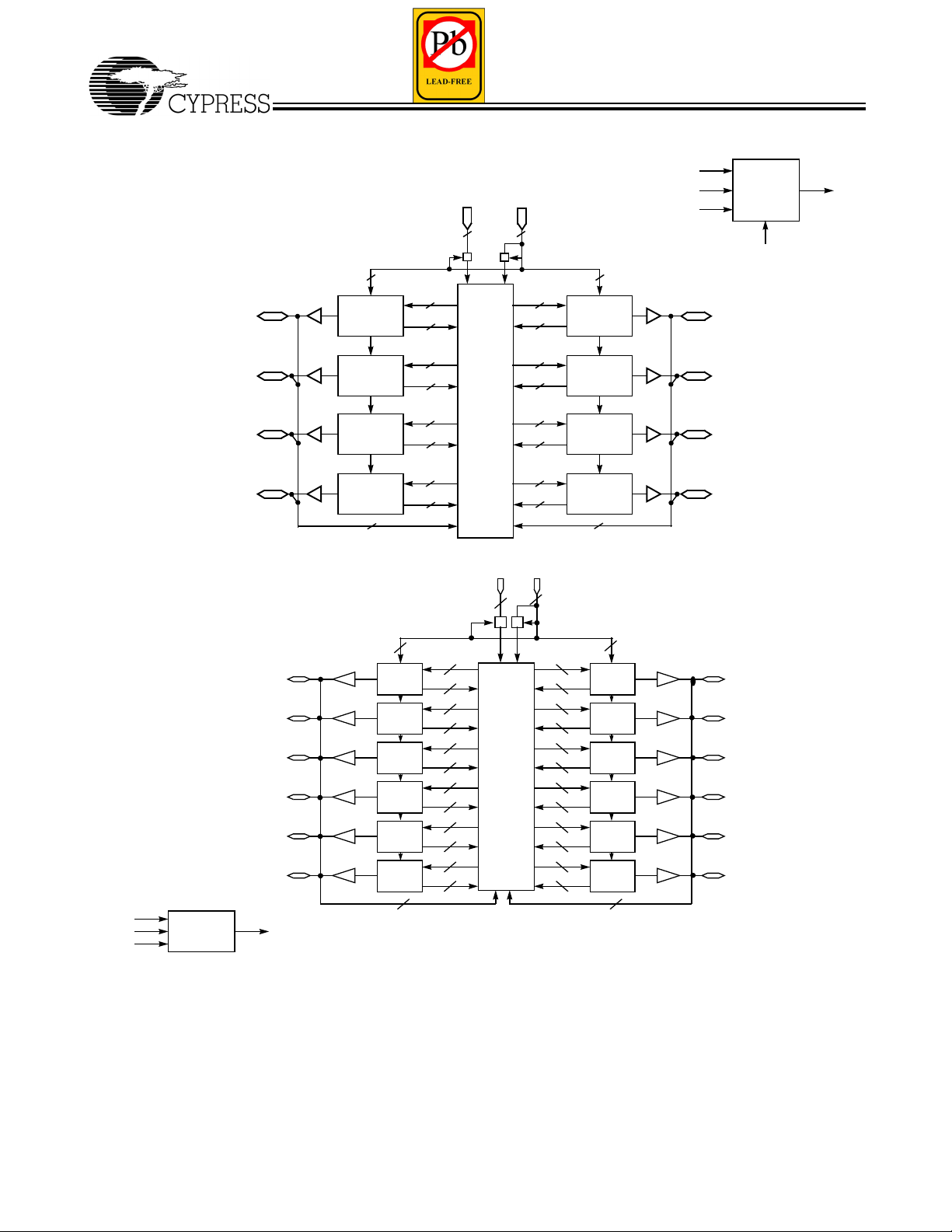
Logic Block Diagrams (continued)
Ultra37000 CPLD Family
CY37128/CY37128V
I/O
–I/O
0
I/O16–I/O
I/O32–I/O
I/O28–I/O
CY37192/CY37192V
15
31
47
63
16 I/Os
16 I/Os
16 I/Os
16 I/Os
CLOCK
INPUTS
INPUTS
41
INPUT
MACROCELL
INPUT/CLOCK
MACROCELLS
4 4
LOGIC
BLOCK
A
LOGIC
BLOCK
B
LOGIC
BLOCK
C
LOGIC
BLOCK
D
64
36
16
36
16
PIM
36
16
36
16
36 36
Input
1
16
36
16
Clock/
Input
16
36
16
LOGIC
BLOCK
LOGIC
BLOCK
LOGIC
BLOCK
LOGIC
BLOCK
64
4
TDI
TCK
TMS
JTAG Tap
Controller
JTAG
EN
TDO
16 I/Os
I/O
–I/O
112
H
16 I/Os
G
I/O96–I/O
127
111
16 I/Os
F
I/O80–I/O
95
16 I/Os
E
I/O64–I/O
79
TDI
TCK
TMS
JTAG Tap
Controller
–I/O
I/O
0
I/O10–I/O
I/O20–I/O
I/O30–I/O
I/O40–I/O
I/O50–I/O
10 I/Os
9
10 I/Os
19
10 I/Os
29
10 I/Os
39
10 I/Os
49
10 I/Os
59
TDO
LOGIC
BLOCK
L
LOGIC
BLOCK
K
LOGIC
BLOCK
J
LOGIC
BLOCK
I
LOGIC
BLOCK
H
LOGIC
BLOCK
G
6060
4
10 I/Os
I/O
–I/O
110
119
10 I/Os
I/O
–I/O
100
109
10 I/Os
I/O90–I/O
99
10 I/Os
I/O80–I/O
89
10 I/Os
I/O70–I/O
79
10 I/Os
I/O60–I/O
69
4
LOGIC
BLOCK
A
LOGIC
BLOCK
B
LOGIC
BLOCK
C
LOGIC
BLOCK
D
LOGIC
BLOCK
E
LOGIC
BLOCK
F
36
16
36
16
36
16
36
16
36
16
36
16
PIM
36
16
36
16
36
16
36
16
36
16
36
16
Document #: 38-03007 Rev. *E Page 10 of 64
[+] Feedback
Page 11
Logic Block Diagrams (continued)
CY37256/CY37256V
Input
1
Clock/
Input
Ultra37000 CPLD Family
4
TDI
TCK
TMS
I/O
I/O12−I/O
I/O24−I/O
I/O36−I/O
I/O48−I/O
I/O60−I/O
I/O72−I/O
I/O84−I/O
JTAG Tap
Controller
0
−I/O
12 I/Os
11
12 I/Os
23
12 I/Os
35
12 I/Os
47
12 I/Os
59
12 I/Os
71
12 I/Os
83
12 I/Os
95
TDO
4
LOGIC
BLOCK
A
LOGIC
BLOCK
B
LOGIC
BLOCK
C
LOGIC
BLOCK
D
LOGIC
BLOCK
E
LOGIC
BLOCK
F
LOGIC
BLOCK
G
LOGIC
BLOCK
H
36
16
36
16
36
16
36
16
36
PIM
16
36
16
36
16
36
16
96
36
LOGIC
BLOCK
16
36
16
36
16
36
16
36
16
36
16
36
16
36
16
P
LOGIC
BLOCK
O
LOGIC
BLOCK
N
LOGIC
BLOCK
M
LOGIC
BLOCK
L
LOGIC
BLOCK
K
LOGIC
BLOCK
J
LOGIC
BLOCK
I
12 I/Os
12 I/Os
12 I/Os
12 I/Os
12 I/Os
12 I/Os
12 I/Os
12 I/Os
I/O
−I/O
180
I/O
−I/O
168
I/O
−I/O
156
I/O
−I/O
144
I/O
−I/O
132
I/O
−I/O
120
I/O
−I/O
108
I/O96−I/O
191
179
167
155
143
131
119
107
96
4
Document #: 38-03007 Rev. *E Page 11 of 64
[+] Feedback
Page 12
Logic Block Diagrams (continued)
Ultra37000 CPLD Family
CY37384/CY37384V
I/O
0
I/O12−I/O
I/O24−I/O
I/O
36
I/O48−I/O
I/O60−I/O
I/O72−I/O
I/O
84
−I/O
−I/O
−I/O
12 I/Os
11
12 I/Os
23
12 I/Os
35
12 I/Os
47
12 I/Os
59
12 I/Os
71
12 I/Os
83
12 I/Os
95
4
LOGIC
BLOCK
AA
LOGIC
BLOCK
AB
LOGIC
BLOCK
AC
LOGIC
BLOCK
AD
LOGIC
BLOCK
AE
LOGIC
BLOCK
AF
LOGIC
BLOCK
AG
LOGIC
BLOCK
AH
LOGIC
BLOCK
AI
LOGIC
BLOCK
AJ
LOGIC
BLOCK
AK
LOGIC
BLOCK
AL
36
16
36
16
36
16
36
16
36
16
36
16
36
16
36
16
36
16
36
16
36
16
36
16
Input
1
PIM
Clock/
Input
4
4
36
LOGIC
BLOCK
16
36
16
36
16
36
16
36
16
36
16
36
16
36
16
36
16
36
16
36
16
36
16
BL
LOGIC
BLOCK
BK
LOGIC
BLOCK
BJ
LOGIC
BLOCK
BI
LOGIC
BLOCK
BH
LOGIC
BLOCK
BG
LOGIC
BLOCK
BF
LOGIC
BLOCK
BE
LOGIC
BLOCK
BD
LOGIC
BLOCK
BC
LOGIC
BLOCK
BB
LOGIC
BLOCK
BA
12 I/Os
12 I/Os
12 I/Os
12 I/Os
12 I/Os
12 I/Os
12 I/Os
12 I/Os
I/O
I/O
I/O
I/O
I/O
I/O
I/O
I/O
168
156
144
132
120
108
96
96
−I/O
−I/O
−I/O
−I/O
−I/O
−I/O
−I/O
−I/O
191
179
167
155
143
131
119
107
TDI
TCK
TMS
JTAG Tap
Controller
TDO
96
96
Document #: 38-03007 Rev. *E Page 12 of 64
[+] Feedback
Page 13
Logic Block Diagrams (continued)
Ultra37000 CPLD Family
CY37512/CY37512V
I/O
I/O12−I/O
I/O24−I/O
I/O36−I/O
I/O48−I/O
I/O60−I/O
I/O72−I/O
I/O84−I/O
I/O
I/O
108
I/O
120
Input
Clock/
Input
1
4
12 I/Os
−I/O
0
11
12 I/Os
23
12 I/Os
35
12 I/Os
47
12 I/Os
59
12 I/Os
71
12 I/Os
83
12 I/Os
95
12 I/Os
−I/O
96
107
12 I/Os
−I/O
119
12 I/Os
−I/O
131
LOGIC
BLOCK
AA
LOGIC
BLOCK
AB
LOGIC
BLOCK
AC
LOGIC
BLOCK
AD
LOGIC
BLOCK
AE
LOGIC
BLOCK
AF
LOGIC
BLOCK
AG
LOGIC
BLOCK
AH
LOGIC
BLOCK
AI
LOGIC
BLOCK
AJ
LOGIC
BLOCK
AK
LOGIC
BLOCK
AL
LOGIC
BLOCK
AM
LOGIC
BLOCK
AN
LOGIC
BLOCK
AO
LOGIC
BLOCK
AP
36
16
36
16
36
16
36
16
36
16
36
16
36
16
36
16
36
PIM
16
36
16
36
16
36
16
36
16
36
16
36
16
36
16
4
4
36
LOGIC
BLOCK
16
36
16
36
16
36
16
36
16
36
16
36
16
36
16
36
16
36
16
36
16
36
16
36
16
36
16
36
16
36
16
BP
LOGIC
BLOCK
BO
LOGIC
BLOCK
BN
LOGIC
BLOCK
BM
LOGIC
BLOCK
BL
LOGIC
BLOCK
BK
LOGIC
BLOCK
BJ
LOGIC
BLOCK
BI
LOGIC
BLOCK
BH
LOGIC
BLOCK
BG
LOGIC
BLOCK
BF
LOGIC
BLOCK
BE
LOGIC
BLOCK
BD
LOGIC
BLOCK
BC
LOGIC
BLOCK
BB
LOGIC
BLOCK
BA
12 I/Os
12 I/Os
12 I/Os
12 I/Os
12 I/Os
12 I/Os
12 I/Os
12 I/Os
12 I/Os
12 I/Os
12 I/Os
I/O
I/O
I/O
I/O
I/O
I/O
I/O
I/O
I/O
I/O
I/O
252
240
228
216
204
192
180
168
156
144
132
−I/O
−I/O
−I/O
−I/O
−I/O
−I/O
−I/O
−I/O
−I/O
−I/O
−I/O
263
251
239
227
215
203
191
179
167
155
143
132132
TDI
TCK
TMS
JTAG Tap
Controller
TDO
Document #: 38-03007 Rev. *E Page 13 of 64
[+] Feedback
Page 14
Ultra37000 CPLD Family
5.0V Device Characteristics
Maximum Ratings
(Above which the useful life may be impaired. For user guidelines, not tested.)
Storage Temperature .................................–65°C to +150°C
Ambient Temperature with
Power Applied.............................................–55°C to +125°C
Supply Voltage to Ground Potential............... –0.5V to +7.0V
Operating Range
Range Ambient Temperature
[2]
[2]
Junction Temperature Output Condition V
DC Voltage Applied to Outputs
in High-Z State................................................–0.5V to +7.0V
DC Input Voltage ............................................–0.5V to +7.0V
DC Program Voltage............................................. 4.5 to 5.5V
Current into Outputs .................................................... 16 mA
Static Discharge Voltage...........................................> 2001V
(per MIL-STD-883, Method 3015)
Latch-up Current.....................................................> 200 mA
CC
V
CCO
Commercial 0°C to +70°C 0°C to +90°C 5V 5V ± 0.25V 5V ± 0.25V
3.3V 5V ± 0.25V 3.3V ± 0.3V
Industrial –40°C to +85°C –40°C to +105°C 5V 5V ± 0.5V 5V ± 0.5V
3.3V 5V ± 0.5V 3.3V ± 0.3V
[3]
Military
–55°C to +125°C –55°C to +130°C 5V 5V ± 0.5V 5V ± 0.5V
3.3V 5V ± 0.5V 3.3V ± 0.3V
5.0V Device Electrical Characteristics Over the Operating Range
Parameter Description Test Conditions Min. Ty p. Max. Unit
V
OH
Output HIGH Voltage VCC = Min. IOH = –3.2 mA (Com’l/Ind)
IOH = –2.0 mA (Mil)
V
OHZ
Output HIGH Voltage with
Output Disabled
[5]
VCC = Max. IOH = 0 µA (Com’l)
IOH = 0 µA (Ind/Mil)
IOH = –100 µA (Com’l)
IOH = –150 µA (Ind/Mil)
V
OL
Output LOW Voltage VCC = Min. IOL = 16 mA (Com’l/Ind)
IOL = 12 mA (Mil)
V
IH
V
IL
I
IX
I
OZ
I
OS
I
BHL
I
BHH
I
BHLO
I
BHHO
Notes:
2. Normal Programming Conditions apply across Ambient Temperature Range for specified programming methods. For more information on programming the
Ultra37000 Family devices, please refer to the Application Note titled “An Introduction to In System Reprogramming with the Ultra37000.”
3. T
A
4. I
OH
5. Tested initially and after any design or process changes that may affect these parameters.
6. When the I/O is output disabled, the bus-hold circuit can weakly pull the I/O to above 3.6V if no leakage current is allowed. Note that all I/Os are output disabled
during ISR programming. Refer to the application note “Understanding Bus-Hold” for additional information.
7. These are absolute values with respect to device ground. All overshoots due to system or tester noise are included.
8. Not more than one output should be tested at a time. Duration of the short circuit should not exceed 1 second. V
problems caused by tester ground degradation.
Input HIGH Voltage Guaranteed Input Logical HIGH Voltage for all Inputs
Input LOW Voltage Guaranteed Input Logical LOW Voltage for all Inputs
Input Load Current VI = GND OR VCC, Bus-Hold Disabled –10 10 µA
Output Leakage Current VO = GND or VCC, Output Disabled, Bus-Hold Disabled –50 50 µA
Output Short Circuit Current
Input Bus-Hold LOW
[5, 8]
VCC = Max., V
= 0.5V –30 –160 mA
OUT
VCC = Min., VIL = 0.8V +75 µA
Sustaining Current
Input Bus-Hold HIGH
VCC = Min., VIH = 2.0V –75 µA
Sustaining Current
Input Bus-Hold LOW
VCC = Max. +500 µA
Overdrive Current
Input Bus-Hold HIGH
VCC = Max. –500 µA
Overdrive Current
is the “Instant On” case temperature.
= –2 mA, IOL = 2 mA for TDO.
[4]
2.4 V
[4]
[6]
[6]
[4]
= 0.5V has been chosen to avoid test
OUT
2.4 V
[6]
[6]
[4]
[7]
2.0 V
[7]
–0.5 0.8 V
4.2 V
4.5 V
3.6 V
3.6 V
0.5 V
0.5 V
CCmax
V
Document #: 38-03007 Rev. *E Page 14 of 64
[+] Feedback
Page 15
Ultra37000 CPLD Family
Inductance
Parameter Description Test Conditions
L Maximum Pin
Capacitance
[5]
Inductance
[5]
V
= 5.0V
IN
at f = 1 MHz
44-Lead
TQFP
44-Lead
PLCC
44-Lead
CLCC
84-Lead
PLCC
84-Lead
CLCC
100-Lead
TQFP
160-Lead
TQFP
208-Lead
PQFP Unit
25285 8 9 11nH
Parameter Description Test Conditions Max. Unit
C
I/O
C
CLK
C
DP
Endurance Characteristics
Input/Output Capacitance VIN = 5.0V at f = 1 MHz at TA = 25°C 10 pF
Clock Signal Capacitance VIN = 5.0V at f = 1 MHz at TA = 25°C 12 pF
Dual-Function Pins
[5]
[9]
VIN = 5.0V at f = 1 MHz at TA = 25°C 16 pF
Parameter Description Test Conditions Min. Typ . Unit
N Minimum Reprogramming Cycles Normal Programming Conditions
3.3V Device Characteristics
Maximum Ratings
(Above which the useful life may be impaired. For user guidelines, not tested.)
Storage Temperature .................................–65°C to +150°C
Ambient Temperature with
Power Applied.............................................–55°C to +125°C
Supply Voltage to Ground Potential............... –0.5V to +4.6V
Operating Range
[2]
Range Ambient Temperature
DC Voltage Applied to Outputs
in High-Z State................................................–0.5V to +7.0V
DC Input Voltage ............................................–0.5V to +7.0V
DC Program Voltage............................................. 3.0 to 3.6V
Current into Outputs ......................................................8 mA
Static Discharge Voltage...........................................> 2001V
(per MIL-STD-883, Method 3015)
Latch-up Current.....................................................> 200 mA
[2]
Junction Temperature V
[2]
1,000 10,000 Cycles
[10]
CC
Commercial 0°C to +70°C 0°C to +90°C 3.3V ± 0.3V
Industrial –40°C to +85°C –40°C to +105°C 3.3V ± 0.3V
[3]
Military
–55°C to +125°C –55°C to +130°C 3.3V ± 0.3V
3.3V Device Electrical Characteristics Over the Operating Range
Parameter Description Test Conditions Min. Max. Unit
V
OH
Output HIGH Voltage VCC = Min. IOH = –4 mA (Com’l)
IOH = –3 mA (Mil)
V
OL
Output LOW Voltage VCC = Min. IOL = 8 mA (Com’l)
IOL = 6 mA (Mil)
V
IH
V
IL
I
IX
I
OZ
I
OS
I
BHL
I
BHH
I
BHLO
I
BHHO
Notes:
9. Dual pins are I/O with JTAG pins.
10. For CY37064VP100-143AC, CY37064VP100-143BBC, CY37064VP44-143AC, CY37064VP48-143BAC; Operating Range: V
Input HIGH Voltage Guaranteed Input Logical HIGH Voltage for
all Inputs
Input LOW Voltage Guaranteed Input Logical LOW Voltage for
all Inputs
[7]
[7]
Input Load Current VI = GND OR VCC, Bus-Hold Disabled –10 10 µA
Output Leakage Current VO = GND or VCC, Output Disabled,
Bus-Hold Disabled
Output Short Circuit Current
[5, 8]
VCC = Max., V
= 0.5V –30 –160 mA
OUT
Input Bus-Hold LOW Sustaining Current VCC = Min., VIL = 0.8V +75 µA
Input Bus-Hold HIGH Sustaining Current VCC = Min., VIH = 2.0V –75 µA
Input Bus-Hold LOW Overdrive Current VCC = Max. +500 µA
Input Bus-Hold HIGH Overdrive Current VCC = Max. –500 µA
[4]
[4]
[4]
[4]
2.4 V
0.5 V
2.0 5.5 V
–0.5 0.8 V
–50 50 µA
is 3.3V± 0.16V.
CC
Document #: 38-03007 Rev. *E Page 15 of 64
[+] Feedback
Page 16
Ultra37000 CPLD Family
Inductance
Parameter Description Test Conditions
L Maximum Pin
Capacitance
[5]
Inductance
[5]
V
= 3.3V
IN
at f = 1 MHz
44-
Lead
TQFP
44-
Lead
PLCC
44-
Lead
CLCC
84-
Lead
PLCC
84-
Lead
CLCC
100-
Lead
TQFP
160-
Lead
TQFP
208-
Lead
PQFP Unit
252858911nH
Parameter Description Test Conditions Max. Unit
C
I/O
C
CLK
C
DP
Endurance Characteristics
Input/Output Capacitance VIN = 3.3V at f = 1 MHz at TA = 25°C 8 pF
Clock Signal Capacitance VIN = 3.3V at f = 1 MHz at TA = 25°C 12 pF
Dual Functional Pins
[5]
[9]
VIN = 3.3V at f = 1 MHz at TA = 25°C 16 pF
Parameter Description Test Conditions Min. Typ . Unit
N Minimum Reprogramming Cycles Normal Programming Conditions
[2]
1,000 10,000 Cycles
AC Characteristics
5.0V AC Test Loads and Waveforms
5 pF
238Ω (COM'L)
319Ω (MIL)
170Ω (COM'L)
236Ω (MIL)
3.0V
GND
ALL INPUT PULSES
90%
10%
<2 ns
(c)
238Ω (COM'L)
5V
OUTPUT
INCLUDING
JIG AND
SCOPE
Equivalent to: THÉVENIN EQUIVALENT
OUTPUT
319Ω (MIL)
35 pF
170Ω (COM'L)
236Ω (MIL)
(a) (b)
99Ω (COM'L)
136Ω (MIL)
5V
OUTPUT
INCLUDING
JIG AND
SCOPE
2.08V (COM'L)
2.13V (MIL)
90%
10%
<2 ns
5 OR 35 pF
3.3V AC Test Loads and Waveforms
5 pF
295Ω (COM'L)
393Ω (MIL)
340Ω (COM'L)
453Ω (MIL)
3.0V
GND
<2 ns
ALL INPUT PULSES
90%
10%
(c)
90%
10%
<2 ns
295Ω (COM'L)
3.3V
OUTPUT
INCLUDING
JIG AND
SCOPE
Equivalent to: THÉVENIN EQUIVALENT
OUTPUT
393Ω (MIL)
35 pF
340Ω (COM'L)
453Ω (MIL)
(a) (b)
158Ω (COM’L)
270Ω (MIL)
5 OR 35 pF
3.3V
OUTPUT
INCLUDING
JIG AND
SCOPE
1.77V (COM'L)
1.77V (MIL)
Document #: 38-03007 Rev. *E Page 16 of 64
[+] Feedback
Page 17
Ultra37000 CPLD Family
t
ER(–)
t
ER(+)
t
EA(+)
t
EA(–)
[11]
V
X
1.5V
2.6V
1.5V
V
the
Output Waveform—Measurement Level
V
OH
0.5V
0.5V
V
OL
0.5V
V
X
V
X
0.5V
V
X
V
X
V
OH
V
OL
Parameter
(d) Test Waveforms
Switching Characteristics Over the Operating Range
[12]
Parameter Description Unit
Combinatorial Mode Parameters
[13, 14, 15]
t
PD
t
PDL
t
PDLL
[13, 14, 15]
t
EA
[11, 13]
t
ER
[13, 14, 15]
[13, 14, 15]
Input to Combinatorial Output ns
Input to Output Through Transparent Input or Output Latch ns
Input to Output Through Transparent Input and Output Latches ns
Input to Output Enable ns
Input to Output Disable ns
Input Register Parameters
t
WL
t
WH
t
IS
t
IH
t
ICO
t
ICOL
[13, 14, 15]
[13, 14, 15]
Clock or Latch Enable Input LOW Time
Clock or Latch Enable Input HIGH Time
Input Register or Latch Set-up Time ns
Input Register or Latch Hold Time ns
Input Register Clock or Latch Enable to Combinatorial Output ns
Input Register Clock or Latch Enable to Output Through Transparent Output Latch ns
[8]
[8]
Synchronous Clocking Parameters
[14, 15]
t
CO
[13]
t
S
t
H
[13, 14, 15]
t
CO2
[13]
t
SCS
[13]
t
SL
t
HL
Notes:
measured with 5-pF AC Test Load and tEA measured with 35-pF AC Test Load.
11. t
ER
12. All AC parameters are measured with two outputs switching and 35-pF AC Test Load.
13. Logic Blocks operating in Low-Power Mode, add t
14. Outputs using Slow Output Slew Rate, add t
15. When V
= 3.3V, add t
CCO
Synchronous Clock (CLK0, CLK1, CLK2, or CLK3) or Latch Enable to Output ns
Set-Up Time from Input to Sync. Clk (CLK0, CLK1, CLK2, or CLK3) or Latch Enable ns
Register or Latch Data Hold Time ns
Output Synchronous Clock (CLK0, CLK1, CLK2, or CLK3) or Latch Enable to Combinatorial Output
Delay (Through Logic Array)
Output Synchronous Clock (CLK0, CLK1, CLK2, or CLK3) or Latch Enable to Output Synchronous
Clock (CLK
, CLK1, CLK2, or CLK3) or Latch Enable (Through Logic Array)
0
Set-Up Time from Input Through Transparent Latch to Output Register Synchronous Clock (CLK0
CLK
, CLK2, or CLK3) or Latch Enable
1
Hold Time for Input Through Transparent Latch from Output Register Synchronous Clock (CLK0,
CLK
, CLK2, or CLK3) or Latch Enable
1
to this spec.
LP
to this spec.
to this spec.
3.3IO
SLEW
ns
ns
ns
ns
ns
ns
Document #: 38-03007 Rev. *E Page 17 of 64
[+] Feedback
Page 18
Ultra37000 CPLD Family
Switching Characteristics Over the Operating Range (continued)
[12]
Parameter Description Unit
Product Term Clocking Parameters
[13, 14, 15]
t
COPT
t
SPT
t
HPT
t
ISPT
t
IHPT
t
CO2PT
[13]
[13, 14, 15]
Product Term Clock or Latch Enable (PTCLK) to Output ns
Set-Up Time from Input to Product Term Clock or Latch Enable (PTCLK) ns
Register or Latch Data Hold Time ns
Set-Up Time for Buried Register used as an Input Register from Input to Product Term Clock or
Latch Enable (PTCLK)
Buried Register Used as an Input Register or Latch Data Hold Time ns
Product Term Clock or Latch Enable (PTCLK) to Output Delay (Through Logic Array) ns
Pipelined Mode Parameters
[13]
t
ICS
Input Register Synchronous Clock (CLK0, CLK1, CLK2, or CLK3) to Output Register Synchronous
Clock (CLK
, CLK1, CLK2, or CLK3)
0
Operating Frequency Parameters
f
MAX1
f
MAX2
f
MAX3
f
MAX4
Maximum Frequency with Internal Feedback (Lesser of 1/t
Maximum Frequency Data Path in Output Registered/Latched Mode (Lesser of 1/(tWL + tWH),
1/(t
S+tH
), or 1/tCO)
[5]
, 1/(tS + tH), or 1/tCO)
SCS
Maximum Frequency with External Feedback (Lesser of 1/(tCO + tS) or 1/(tWL + tWH)
Maximum Frequency in Pipelined Mode (Lesser of 1/(tCO + tIS), 1/t
or 1/t
SCS
[5]
)
, 1/(tWL + tWH), 1/(tIS + tIH),
ICS
[5]
[5]
Reset/Preset Parameters
t
RW
[13]
t
RR
[13, 14, 15]
t
RO
t
PW
[13]
t
PR
[13, 14, 15]
t
PO
Asynchronous Reset Width
Asynchronous Reset Recovery Time
Asynchronous Reset to Output ns
Asynchronous Preset Width
Asynchronous Preset Recovery Time
Asynchronous Preset to Output ns
[5]
[5]
[5]
[5]
User Option Parameters
t
LP
t
SLEW
t
3.3IO
Low Power Adder ns
Slow Output Slew Rate Adder ns
3.3V I/O Mode Timing Adder
[5]
JTAG Timing Parameters
t
S JTAG
t
H JTAG
t
CO JTAG
f
JTAG
Set-up Time from TDI and TMS to TCK
Hold Time on TDI and TMS
Falling Edge of TCK to TDO
[5]
[5]
Maximum JTAG Tap Controller Frequency
[5]
[5]
ns
ns
MHz
MHz
MHz
MHz
ns
ns
ns
ns
ns
ns
ns
ns
ns
Document #: 38-03007 Rev. *E Page 18 of 64
[+] Feedback
Page 19
Ultra37000 CPLD Family
Switching Characteristics Over the Operating Range
200 MHz 167 MHz
Parameter
Min.
Max.
Min.
Combinatorial Mode Parameters
[13, 14, 15]
t
PD
t
PDL
t
PDLL
[13, 14, 15]
t
EA
[11, 13]
t
ER
[13, 14, 15]
[13, 14, 15]
6 6.5 7.5 8.5 10 12 15 20 ns
11 12.5 14.5 16 16.5 17 19 22 ns
12 13.5 15.5 17 17.5 18 20 24 ns
8 8.5 11 13 14 16 19 24 ns
8 8.5 11 13 14 16 19 24 ns
Input Register Parameters
t
WL
t
WH
t
IS
t
IH
t
ICO
t
ICOL
[13, 14, 15]
[13, 14, 15]
2.5 2.5 2.5 2.5 3 3 4 5 ns
2.5 2.5 2.5 2.5 3 3 4 5 ns
2 222 2 2.5 3 4ns
2 222 2 2.5 3 4ns
11 11 11 12.5 12.5 16 19 24 ns
12 12 12 14 16 18 21 26 ns
Synchronous Clocking Parameters
[14, 15]
t
CO
t
S
t
H
t
CO2
t
SCS
t
SL
t
HL
[13]
[13, 14, 15]
[13]
[13]
4 4 4.5 6 6.5
44555.5
0000 0 0 0 0ns
9.5 10 11 12 14 16 19 24 ns
5 66.57 8
7.5 7.5 8.5 9 10 12 15 15 ns
0 000 0 0 0 0ns
Product Term Clocking Parameters
[13, 14, 15]
t
COPT
t
SPT
t
HPT
t
ISPT
t
IHPT
t
CO2PT
15]
[13]
[13, 14,
7101013 13 13 1520ns
2.5 2.5 2.5 3 5 5.5 6 7 ns
2.5 2.5 2.5 3 5 5.5 6 7 ns
0000 00 00ns
6 6.5 6.5 7.5 9 11 14 19 ns
12 14 15 19 19 21 24 30 ns
154 MHz 143 MHz 125 MHz 100 MHz 83 MHz 66 MHz
Max.
Min.
Max.
Min.
[12]
Max.
[16]
[16]
Min.
Min.
Max.
[18]
8
[18]
8
[16]
Max.
Min.
[17]
6
6.5
Max.
[17]
10 12 15 ns
Min.
Unit
Max.
10 ns
10 ns
Pipelined Mode Parameters
t
ICS
[13]
56678
[16]
10 12 15 ns
Operating Frequency Parameters
f
MAX1
f
MAX2
f
MAX3
f
MAX4
200 167 154 143 125
200 200 200 167 154 153
125 125 105 91 83 80
167 167 154 125 118 100 83 66 MHz
[16]
100 83 66 MHz
[17]
[17]
[18]
125
100 MHz
62.5 50 MHz
Reset/Preset Parameters
t
RW
[13]
t
RR
Notes:
16. The following values correspond to the CY37512 and CY37384 devices: t
17. The following values correspond to the CY37192V and CY37256V devices: t
for the CY37512 devices: t
18. The following values correspond to the CY37512V and CY37384V devices: t
8 8 8 8 10 12 15 20 ns
10 10 10 10 12 14 17 22 ns
= 7 ns.
S
= 5 ns, tS = 6.5 ns, t
CO
= 6 ns, tS = 7 ns, f
CO
= 6.5 ns, tS = 9.5 ns, and f
CO
= 8.5 ns, t
SCS
= 143 MHz, f
MAX2
ICS
= 105 MHz.
MAX2
= 8.5 ns, f
= 77 MHz, and f
MAX3
MAX1
= 118 MHz.
MAX4
= 100 MHz; and
Document #: 38-03007 Rev. *E Page 19 of 64
[+] Feedback
Page 20
Ultra37000 CPLD Family
Switching Characteristics Over the Operating Range (continued)
200 MHz 167 MHz
Parameter
[13, 14, 15]
t
RO
t
PW
[13]
t
PR
[13, 14, 15]
t
PO
Min.
12 13 13 14 15 18 21 26 ns
8 8 8 8 10 12 15 20 ns
10 10 10 10 12 14 17 22 ns
12 13 13 14 15 18 21 26 ns
User Option Parameters
t
LP
t
SLEW
t
3.3IO
[19]
2.5 2.5 2.5 2.5 2.5 2.5 2.5 2.5 ns
3333 3 3 33ns
0.3 0.3 0.3 0.3 0.3 0.3 0.3 0.3 ns
JTAG Timing Parameters
t
S JTAG
t
H JTAG
t
CO JTAG
f
JTAG
0 000 00 00ns
20 20 20 20 20 20 20 20 ns
20 20 20 20 20 20 20 20 ns
20 20 20 20 20 20 20 20 MHz
Max.
Min.
154 MHz 143 MHz 125 MHz 100 MHz 83 MHz 66 MHz
Max.
Min.
Max.
Min.
Max.
Min.
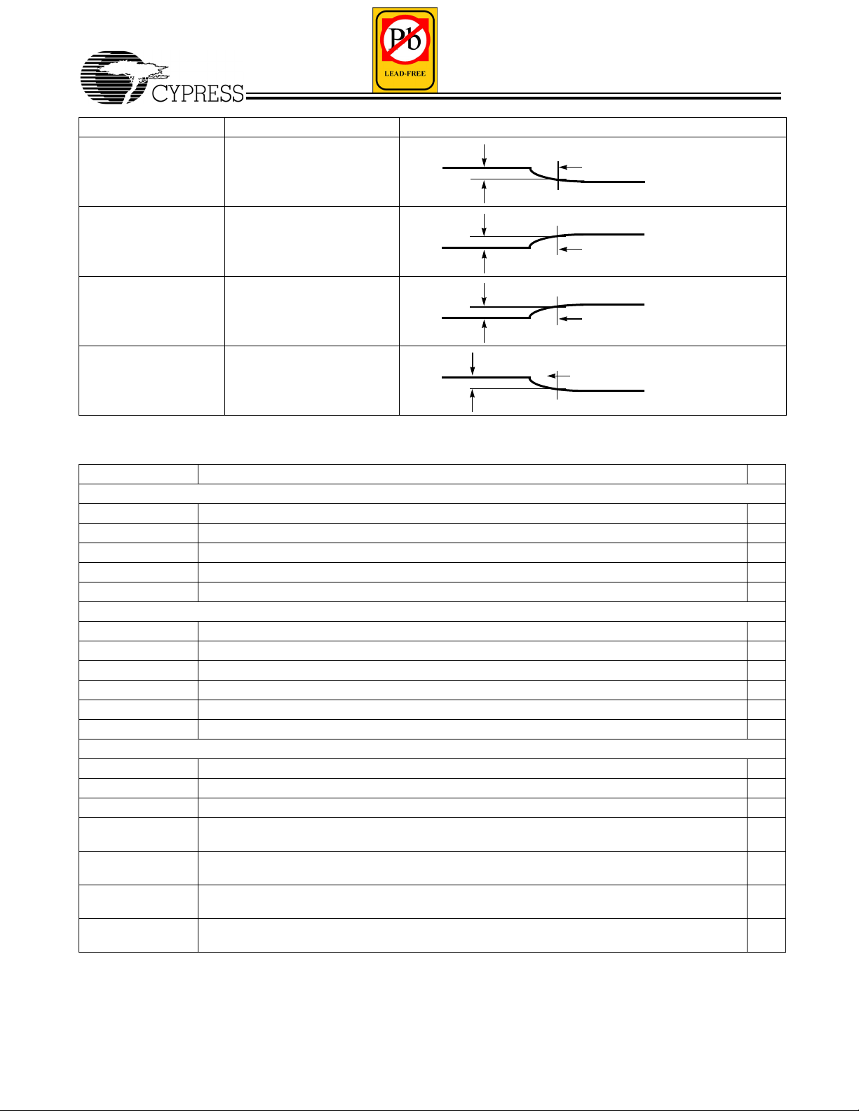
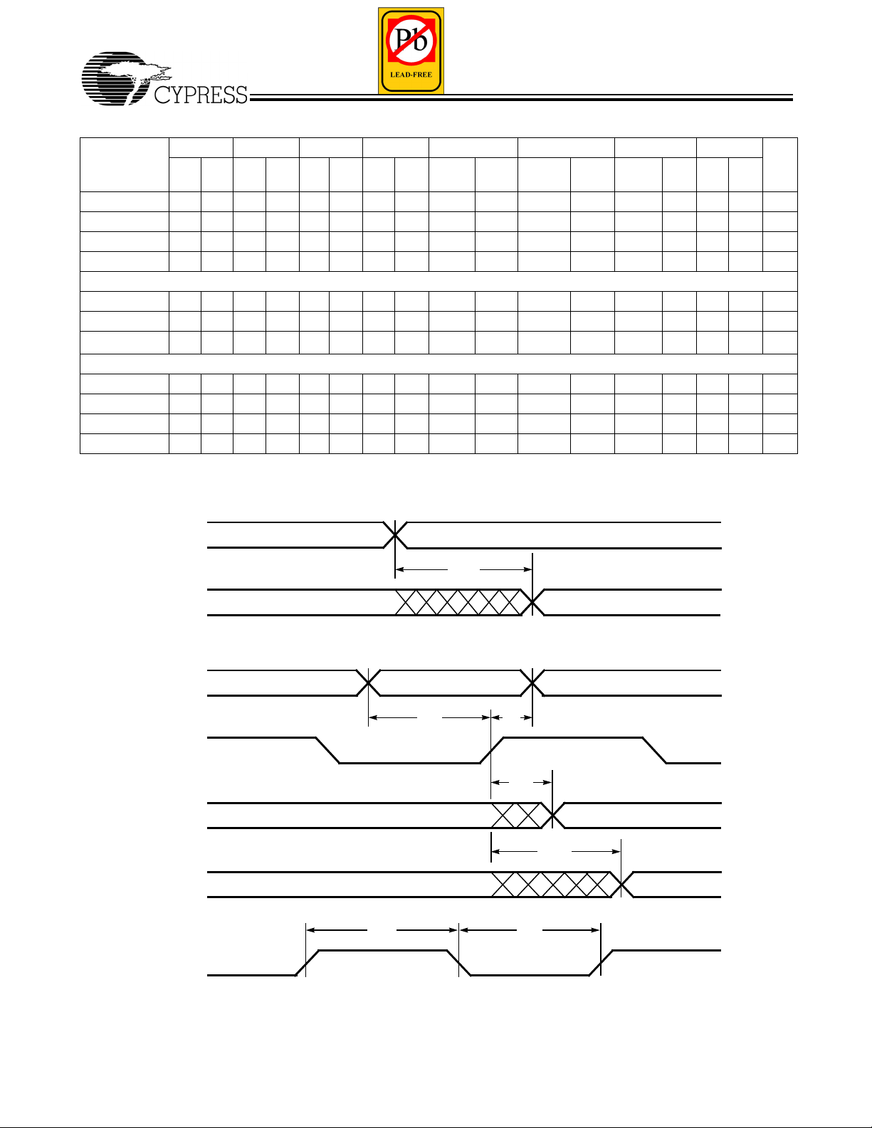
Switching Waveforms
Combinatorial Output
[12]
Max.
Min.
Max.
Min.
Max.
Min.
Unit
Max.
INPUT
COMBINATORIAL
OUTPUT
Registered Output with Synchronous Clocking
INPUT
SYNCHRONOUS
CLOCK
REGISTERED
OUTPUT
REGISTERED
OUTPUT
SYNCHRONOUS
CLOCK
t
WH
t
PD
t
S
t
H
t
CO
t
CO2
t
WL
Note:
19. Only applicable to the 5V devices.
Document #: 38-03007 Rev. *E Page 20 of 64
[+] Feedback
Page 21

Switching Waveforms (continued)
Registered Output with Product Term Clocking Input Going Through the Array
INPUT
Ultra37000 CPLD Family
t
SPT
t
HPT
PRODUCT TERM
CLOCK
t
COPT
REGISTERED
OUTPUT
Registered Output with Product Term Clocking Input Coming From Adjacent Buried Register
INPUT
t
ISPT
t
IHPT
PRODUCT TERM
CLOCK
t
CO2PT
REGISTERED
OUTPUT
Latched Output
INPUT
t
SL
t
HL
LATCH ENABLE
t
PDL
t
CO
LATCHED
OUTPUT
Document #: 38-03007 Rev. *E Page 21 of 64
[+] Feedback
Page 22

Switching Waveforms (continued)
Registered Input
REGISTERED
INPUT
Ultra37000 CPLD Family
INPUT REGISTER
CLOCK
COMBINATORIAL
OUTPUT
CLOCK
Clock to Clock
INPUT REGISTER
CLOCK
OUTPUT
REGISTER CLOCK
Latched Input
LATCHED INPUT
t
WH
t
IS
t
ICS
t
ICO
t
IH
t
WL
t
SCS
LATCH ENABLE
COMBINATORIAL
OUTPUT
LATCH ENABLE
t
PDL
t
IS
t
WH
t
IH
t
ICO
t
WL
Document #: 38-03007 Rev. *E Page 22 of 64
[+] Feedback
Page 23

Switching Waveforms (continued)
Latched Input and Output
LATCHED INPUT
LATCHED
OUTPUT
Ultra37000 CPLD Family
t
PDLL
INPUT LATCH
ENABLE
OUTPUT LATCH
ENABLE
LATCH ENABLE
Asynchronous Reset
INPUT
REGISTERED
OUTPUT
CLOCK
t
ICOL
t
ICS
t
WH
t
SL
t
WL
t
RW
t
RO
t
RR
t
HL
Asynchronous Preset
t
PW
INPUT
t
PO
REGISTERED
OUTPUT
t
PR
CLOCK
Output Enable/Disable
INPUT
t
ER
t
EA
OUTPUTS
Document #: 38-03007 Rev. *E Page 23 of 64
[+] Feedback
Page 24
Power Consumption
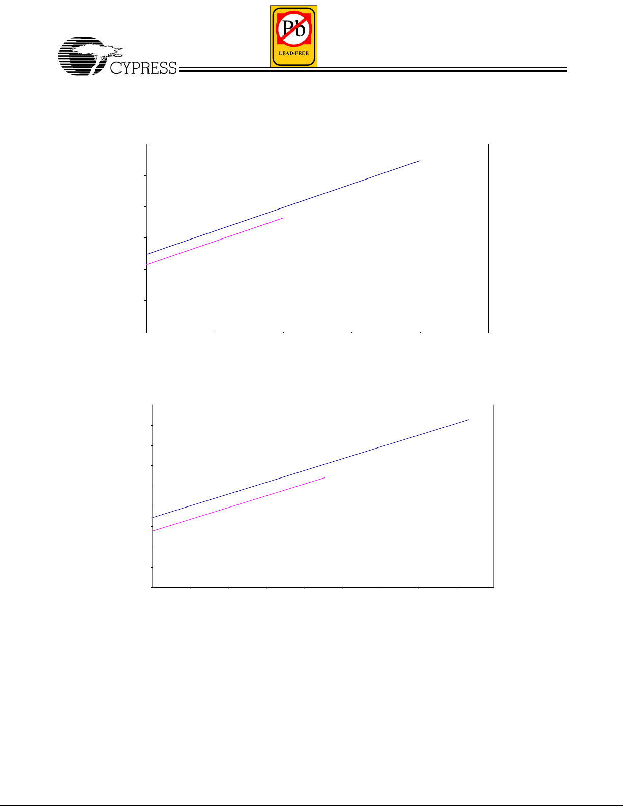
Typical 5.0V Power Consumption
CY37032
60
50
40
30
Icc (mA)
20
10
0
0 50 100 1 50 200 250
Ultra37000 CPLD Family
High Speed
Low Power
Frequency (MHz)
CY37064
The typical pattern is a 16-bit up counter, per logic block, with outputs disabled.
V
= 5.0V, TA = Room Temperature
CC
90
80
70
60
50
Icc (mA)
40
30
20
10
0
0 20 40 60 80 100 120 140 160 180
Frequency (MHz)
Low Power
High Speed
The typical pattern is a 16-bit up counter, per logic block, with outputs disabled.
V
= 5.0V, TA = Room Temperature
CC
Document #: 38-03007 Rev. *E Page 24 of 64
[+] Feedback
Page 25

Typical 5.0V Power Consumption (continued)
CY37128
160
Ultra37000 CPLD Family
CY37192
140
120
100
Low Power
80
Icc (mA)
60
40
20
0
0 20 40 60 80 100 120 140 160 180
Frequency (MHz)
The typical pattern is a 16-bit up counter, per logic block, with outputs disabled.
V
= 5.0V, TA = Room Temperature
CC
300
250
High Speed
High Speed
200
150
Icc (mA)
100
50
0
0 20 40 60 80 100 120 140 160 180
Low Power
Frequency (MHz)
The typical pattern is a 16-bit up counter, per logic block, with outputs disabled.
V
= 5.0V, TA = Room Temperature
CC
Document #: 38-03007 Rev. *E Page 25 of 64
[+] Feedback
Page 26

Typical 5.0V Power Consumption (continued)
CY37256
300
250
200
150
Icc (mA)
100
50
0
0 20 40 60 80 100 120 140 160 180
Ultra37000 CPLD Family
High Speed
Low Power
Frequency (M Hz)
CY37384
The typical pattern is a 16-bit up counter, per logic block, with outputs disabled.
V
= 5.0V, TA = Room Temperature
CC
500
450
400
350
300
250
Icc (mA)
200
150
100
50
0
0 20 40 60 80 100 120 140 160
Low Power
Frequency (MHz)
The typical pattern is a 16-bit up counter, per logic block, with outputs disabled.
V
= 5.0V, TA = Room Temperature
CC
High Speed
Document #: 38-03007 Rev. *E Page 26 of 64
[+] Feedback
Page 27

Typical 5.0V Power Consumption (continued)
CY37512
600
Ultra37000 CPLD Family
500
400
300
Icc (mA)
200
100
0
0 20 40 60 80 100 120 140 160
Typical 3.3V Power Consumption
CY37032V
30
25
Low Power
Frequency (MHz)
The typical pattern is a 16-bit up counter, per logic block, with outputs disabled.
V
= 5.0V, TA = Room Temperature
CC
High Speed
High Speed
20
15
Icc (mA)
10
5
0
0 20 40 60 80 100 120 140 160
Low Power
Frequency (MHz)
The typical pattern is a 16-bit up counter, per logic block, with outputs disabled.
V
= 3.3V, TA = Room Temperature
CC
Document #: 38-03007 Rev. *E Page 27 of 64
[+] Feedback
Page 28

Typical 3.3V Power Consumption (continued)
CY37064V
45
40
35
30
25
Icc (mA)
20
15
10
5
0
0 20 40 60 80 100 120 140
Ultra37000 CPLD Family
High Speed
Low Power
Frequency (MHz)
CY37128V
The typical pattern is a 16-bit up counter, per logic block, with outputs disabled.
V
= 3.3V, TA = Room Temperature
CC
80
70
60
50
40
Icc (mA)
30
20
10
0
0 20 40 60 80 100 120 140
Frequency (M Hz)
Low Power
High Speed
The typical pattern is a 16-bit up counter, per logic block, with outputs disabled.
V
= 3.3V, TA = Room Temperature
CC
Document #: 38-03007 Rev. *E Page 28 of 64
[+] Feedback
Page 29

Typical 3.3V Power Consumption (continued)
CY37192V
120
Ultra37000 CPLD Family
CY37256V
100
80
60
Icc (mA)
40
20
0
0 20 40 60 80 100 120
Frequency (MHz)
Low Power
High Speed
The typical pattern is a 16-bit up counter, per logic block, with outputs disabled.
V
= 3.3V, TA = Room Temperature
CC
140
120
100
High Speed
80
Icc (mA)
60
40
20
0
0 20 40 60 80 100 120
Frequency (M Hz)
Low Power
The typical pattern is a 16-bit up counter, per logic block, with outputs disabled.
V
= 3.3V, TA = Room Temperature
CC
Document #: 38-03007 Rev. *E Page 29 of 64
[+] Feedback
Page 30

Typical 3.3V Power Consumption (continued)
CY37384V
200
Ultra37000 CPLD Family
CY37512V
180
160
140
120
100
Icc (mA)
80
60
40
20
0
0 102030405060708090
Frequency (M Hz)
Low Power
High Speed
The typical pattern is a 16-bit up counter, per logic block, with outputs disabled.
V
= 3.3V, TA = Room Temperature
CC
250
200
High Speed
150
Icc (mA)
100
50
0
0 1020304050 60708090
Frequency (MHz)
Low Power
The typical pattern is a 16-bit up counter, per logic block, with outputs disabled.
V
= 3.3V, TA = Room Temperature
CC
Document #: 38-03007 Rev. *E Page 30 of 64
[+] Feedback
Page 31

Ultra37000 CPLD Family
Pin Configurations
[20]
I/O5/TCK
I/O
I/O
CLK2/I
JTAG
GND
CLK0/I
I/O
I/O
I/O
I/O
EN
10
11
44-pin TQFP (A44)
Top View
0
2
3
4
I/O
I/O
I/O
I/O1I/O
44 43 42 4041 39 38 37 3536 34
1
2
6
3
7
4
0
5
6
7
1
8
8
9
9
10
11
14
/TMS
I/O
15
CC
V
I/O
12
I/O
13
I/O
GND
18 19 20 222113 14 15 171612
GND
CCO
V
16
31
28
I/O29I/O30I/O
I/O
33
32
31
30
29
28
27
26
25
24
23
I/O27/TDI
I/O
26
I/O
25
I/O
24
CLK1/I
4
GND
I
3
CLK3/I
2
I/O
23
I/O
22
I/O
21
20
I/O
I/O18I/O17I/O
/TDO
19
I/O
I/O5/TCK
I/O
I/O
CLK2/I
JTAG
EN
GND
CLK0/I
I/O
I/O
I/O
I/O
44-pin PLCC (J67) / CLCC (Y67)
Top View
2
4
I/O3I/O
65 34 2
7
8
6
9
7
10
0
11
12
13
1
14
8
15
9
16
10
17
11
18
19 20 2221 23 24 2726 2825
12
I/O
I/O
/TMS
13
I/O
14
0
I/O
I/O1I/O
GND
1
15
CC
V
GND
I/O
I/O
CCO
V
43 42 4041
44
16
I/O
17
31
28
I/O29I/O30I/O
I/O
I/O27/TDI
39
I/O
38
37
36
35
34
33
32
31
30
29
18
I/O
I/O
/TDO
20
26
I/O
25
I/O
24
CLK1/I
GND
I
3
CLK3/I
I/O
23
I/O
22
I/O
21
4
2
19
I/O
Document #: 38-03007 Rev. *E Page 31 of 64
[+] Feedback
Page 32

Ultra37000 CPLD Family
Pin Configurations
Note:
20. For 3.3V versions (Ultra37000V), V
[20]
(continued)
48-ball Fine-Pitch BGA (BA50)
Top View
12345678
V
A I/O
5
TCK
BV
CC
CCLK2/ I0I/O7I/O6GND GND I/O25I/O24I
DJTAGENI/O8I/O9GND GND I/O22I/O23CLK3/ I
ECLK0/ I1I/O12I/O11I/O10I/O16I/O20I/O21V
F I/O
13
TMS
= VCC.
CCO
I/O3I/O1I/O31I/O30VCCI/O27
CC
I/O4I/O2I/O0I/O29I/O28I/O26CLK1/ I
VCCI/O14I/O15I/O17I/O18VCCI/O19
84-lead PLCC (J83) / CLCC (Y84)
Top View
7
6
5
4
3
2
1
0
CCO
CC
GND
V
I/O
I/O
I/O
GND
I/O
I/O
I/O
I/O
I/O
V
EN
JTAG
TDI
4
3
2
CC
TDO
63
62616059585756
I/O
I/O
I/O
I/O
I/O
I/O
I/O
I/O
98 67 5
11
10
12
I/O
8
13
I/O
9
I/O
I/O
I/O
I/O
I/O
CCO
GND
I/O
I/O
I/O
I/O
I/O
I/O
I/O
I/O
GND
14
15
11
16
12
17
13
18
14
19
15
20
0
21
22
23
1
16
24
17
25
18
26
19
27
20
28
21
29
22
30
31
23
33
32
34
24
I/O
3736
35 39 44 45
25
I/O
38
/TMS
I/O27I/O28I/O29I/O30I/O
26
I/O
/TCK
10
CLK0/I
V
CLK1/I
I/O
Note:
21. This pin is a N/C, but Cypress recommends that you connect it to V
43
84 8182 80 79
2
83
1
42414340
2
31
I
to ensure future compatibility.
CC
[21]
GND
CCO
V
I/O32I/O33I/O34I/O35I/O36I/O
CC
V
7778 76 75
GND
74
73
I/O
55
I/O
I/O
I/O
I/O
I/O
I/O
I/O
CLK3/I
GND
V
CCO
CLK2/I
I/O
I/O
I/O
I/O
I/O
I/O
I/O
I/O
/TDI
54
53
52
51
50
49
48
4
3
47
46
45
44
43
42
41
40
72
71
70
69
68
67
66
65
64
63
62
61
60
59
58
57
56
55
/TDO
38
54
53525150
39
GND
I/O
4948
4746
37
I/O
Document #: 38-03007 Rev. *E Page 32 of 64
[+] Feedback
Page 33

Ultra37000 CPLD Family
Pin Configurations
TCK
GND
I/O
8
I/O
9
I/O
10
I/O
11
I/O
12
I/O
13
I/O
14
I/O
15
CLK0/I
0
V
CCO
N/C
GND
CLK
1/I1
I/O
16
I/O
17
I/O
18
I/O
19
I/O
20
I/O
21
I/O
22
I/O
23
V
CCO
NC
[20]
(continued)
NC
100 9798 96
99
1
2
3
4
5
6
7
8
9
10
11
12
13
14
15
16
17
18
19
20
21
22
23
24
25
26
27 28 3029 31 32 3534 36 3833
7654321
CCO
I/O
I/O
V
I/O
95 94
I/O
100-lead TQFP (A100)
Top View
0
CCO
I/O
I/O
I/O
GND
I/O
V
89 88 8687 8593 92 84
9091
37
NC
63
CC
V
62616059585756
I/O
I/O
I/O
N/C
I/O
I/O
I/O
I/O
I/O
GND
NC
83 82 81 80 79 78 77 76
75
74
73
72
71
70
69
68
67
66
65
64
63
62
61
60
59
58
57
56
55
54
53
52
51
4241
4039
43 44 45 46 48 49 50
47
TDI
V
CCO
I/O
55
I/O
54
I/O
53
I/O
52
I/O
51
I/O
50
I/O
49
I/O
48
CLK3/I
GND
NC
V
CCO
CLK2/I
I/O
47
I/O
46
I/O
45
I/O
44
I/O
43
I/O
42
I/O
41
I/O
40
GND
NC
4
3
TMS
GND
I/O24I/O25I/O26I/O27I/O28I/O29I/O30I/O
31
I
CCO
V
[21 ]
NC
GND
CC
I/O32I/O33I/O34I/O35I/O36I/O37I/O38I/O
V
39
CCO
TDO
V
2
Document #: 38-03007 Rev. *E Page 33 of 64
[+] Feedback
Page 34

Ultra37000 CPLD Family
Pin Configurations
[20]
(continued)
100-ball Fine-Pitch BGA (BB100) for CY37064V
Top V iew
12345678910
A NC NC I/O7I/O5I/O2I/O62I/O60I/O58I/O57I/O
BI/O9I/O8I/O6I/O4I/O1I/O63VCCI/O59I/O55NC
C I/O10TCK VCCI/O3NC NC I/O61V
D I/O11NC I/O12I/O13I/O0NC I/O51I/O52CLK3/
E I/O14CLK0/
F I/O17NC NC I/O16GND GND NC NC I2I/O
G I/O22CLK1/
H I/O23TMS VCCI/O20NC I/O32I/O42VCCTDO I/O
JNCI/O26I/O28NC I/O31I/O33I/O35I/O37I/O39I/O
K I/O24I/O25I/O27I/O29I/O30I/O34I/O36I/O38NC NC
I/O15NC GND GND I/O48I/O49CLK2/
I
0
I/O21I/O19I/O18I/O46I/O45I/O44NC I/O
I
1
CC
TDI I/O
I/O
I
4
I/O
I
3
56
54
53
50
47
43
41
40
100-ball Fine-Pitch BGA (BB100) for CY37128V
Top V iew
12345678910
A NC I/O9I/O8I/O6I/O3I/O76I/O74I/O72I/O71I/O
B I/O11I/O10I/O7I/O5I/O2I/O77VCCI/O73I/O68I/O
C I/O12I/O
D I/O14NC I/O15I/O16I/O0I/O79I/O63I/O64CLK3/
E I/O17CLK0/
F I/O
22
G I/O27CLK1/
H I/O28I/O
J I/O29I/O32I/O35VCCI/O38I/O41I/O43I/O45I/O48I/O
K I/O30I/O31I/O34I/O36I/O37I/O42I/O44I/O46I/O49NC
VCCI/O4I/O1I/O78I/O75VCCI/O
13
TCK
I/O18I/O19GND GND I/O60I/O61CLK2/
I
0
JTAG
I/O21I/O20GND GND I/O59I/O58I2I/O
EN
I/O26I/O24I/O23I/O56I/O55I/O54NC I/O
I
1
VCCI/O25I/O39I/O40I/O52VCCI/O
33
TMS
TDI
TDO
I/O
67
I/O
I
4
I/O
I
3
I/O
47
70
69
66
65
62
57
53
51
50
Document #: 38-03007 Rev. *E Page 34 of 64
[+] Feedback
Page 35

Ultra37000 CPLD Family
Pin Configurations
CCO
V
GND
I/O
I/O
I/O
I/O
I/O20/TCK
I/O
I/O
I/O
GND
I/O
I/O
I/O
I/O
I/O
I/O
I/O
I/O
CLK0/I
V
CCO
GND
CLK1/I
I/O
I/O
I/O
I/O
I/O
I/O
I/O
I/O
GND
I/O
I/O
I/O
I/O
I/O
I/O
I/O
I/O
V
CCO
16
17
18
19
21
22
23
24
25
26
27
28
29
30
31
0
1
32
33
34
35
36
37
38
39
40
41
42
43
44
45
46
47
16045159461584715748156491555015451153521525315154150551495614857147581465914560144611436214263141
1
2
3
4
5
6
7
8
9
10
11
12
13
14
15
16
17
18
19
20
21
22
23
24
25
26
27
28
29
30
31
32
33
34
35
36
37
38
39
40
[20]
(continued)
15
43
42
41
160-Lead TQFP (A160) / CQFP (U162)
for CY37128(V) and CY37256(V)
Top View
7
GND
I/O8I/O9I/O10I/O11I/O12I/O13I/O14I/O
I/O0I/O1I/O2I/O3I/O4I/O5I/O6I/O
EN
CC
CCO
GND
V
V
JTAG
I/O
124
125
126
127
I/O
I/O
I/O
I/O
120
121
122
123
I/O
I/O
I/O
GND
I/O
116
117
118
119
I/O
I/O
I/O
1406913970138711377213673135741347513376132771317813079129801288112782126
44
6465666768
I/O
125
112
113
114
115
I/O
GND
I/O
I/O
124
123
122
121
120
119
118
117
116
115
114
113
112
111
110
109
108
107
106
105
104
103
102
101
100
99
98
97
96
95
94
93
92
91
90
89
88
87
86
85
84
83
V
CCO
I/O
111
I/O
110
I/O
109
I/O
108
I/O
107
I/O
106
I/O
105
I/O
104
GND
I/O
103
I/O
102
I/O
101
I/O
100
I/O
99
I/O
98
I/O
97
I/O
96
CLK3/I
GND
V
CCO
CLK2/I
I/O
95
I/O
94
I/O
93
I/O
92
I/O
91
I/O
90
I/O
89
I/O
88
GND
I/O
87
I/O
86
I/O
85
I/O
84
I/O
83
I/O
82
I/O
81
I/O
80
GND
/TDI
4
3
GND
I/O48I/O49I/O50I/O51I/O53I/O54I/O55I/O56I/O57I/O58I/O59I/O60I/O61I/O62I/O
/TMS
52
GND
I/O
I
63
CC
CCO
V
GND
I/O64I/O65I/O66I/O67I/O68I/O69I/O70I/O71I/O72I/O73I/O74I/O75I/O78I/O
V
GND
/TDO
76
I/O
I/O
77
79
CCO
V
2
Document #: 38-03007 Rev. *E Page 35 of 64
[+] Feedback
Page 36

Ultra37000 CPLD Family
Pin Configurations
CCO
V
GND
I/O
I/O
I/O
TCK
I/O
I/O
I/O
GND
I/O
I/O
I/O
I/O
I/O
I/O
I/O
I/O
CLK0/I
V
GND
CLK1/I
I/O
I/O
I/O
I/O
I/O
I/O
I/O
I/O
GND
I/O
I/O
I/O
I/O
I/O
I/O
I/O
I/O
V
NC
CCO
CCO
16
17
18
19
20
21
22
23
24
25
26
27
28
29
0
1
30
31
32
33
34
35
36
37
38
39
40
41
42
43
44
45
16045159461584715748156491555015451153521525315154150551495614857147581465914560144611436214263141
1
2
3
4
5
6
7
8
9
10
11
12
13
14
15
16
17
18
19
20
21
22
23
24
25
26
27
28
29
30
31
32
33
34
35
36
37
38
39
40
[20]
(continued)
15
43
42
41
160-Lead TQFP (A160) for CY37192(V)
Top View
105
106
107
108
109
110
111
112
113
114
115
116
117
118
7
GND
I/O8I/O9I/O10I/O11I/O12I/O13I/O14I/O
CCO
V
I/O0I/O1I/O2I/O3I/O4I/O5I/O6I/O
44
119
CC
GND
V
I/O
NC
I/O
I/O
I/O
I/O
I/O
I/O
I/O
GND
I/O
1406913970138711377213673135741347513376132771317813079129801288112782126
6465666768
I/O
I/O
I/O
I/O
125
I/O
124
I/O
123
NC
122
GND
121
120
119
118
117
116
115
114
113
112
111
110
109
108
107
106
105
104
103
102
101
100
V
CCO
I/O
104
I/O
103
I/O
102
TDI
I/O
101
I/O
100
I/O
99
I/O
98
GND
I/O
97
I/O
96
I/O
95
I/O
94
I/O
93
I/O
92
I/O
91
I/O
90
CLK3/I
4
GND
V
CCO
99
98
97
96
95
94
93
92
91
90
89
88
87
86
85
84
83
CLK2/I
I/O
89
I/O
88
I/O
87
I/O
86
I/O
85
I/O
84
I/O
83
I/O
82
GND
I/O
81
I/O
80
I/O
79
I/O
78
I/O
77
I/O
76
I/O
75
NC
GND
3
46
NC
GND
TMS
I/O47I/O48I/O49I/O50I/O51I/O52I/O53I/O54I/O55I/O56I/O57I/O58I/O
I/O
GND
I
59
CC
CCO
V
GND
I/O60I/O61I/O62I/O63I/O64I/O65I/O66I/O67I/O68I/O69I/O70I/O71I/O73I/O
V
GND
TDO
I/O
72
74
CCO
V
2
Document #: 38-03007 Rev. *E Page 36 of 64
[+] Feedback
Page 37

Ultra37000 CPLD Family
Pin Configurations
CC0
CC
V
I/O19I/O18I/O17I/O16I/O15NC
V
207
206
205
GND
I/O
I/O
I/O
I/O
I/O
TCK
I/O
I/O
I/O
I/O
I/O
GND
I/O
I/O
I/O
I/O
I/O
I/O
I/O
I/O
I/O
I/O
CLK0/I
V
GND
CLK1/I
I/O
I/O
I/O
I/O
I/O
I/O
I/O
I/O
I/O
I/O
GND
I/O
I/O
I/O
I/O
I/O
I/O
I/O
I/O
I/O
I/O
V
NC
CCO
NC
NC
CC0
208
1
2
20
3
21
4
22
5
23
6
24
7
8
25
9
26
10
27
11
28
12
29
13
14
30
15
31
16
32
17
33
18
34
19
20
35
21
36
22
37
23
38
24
39
25
0
26
27
28
29
1
30
40
31
41
32
42
33
43
34
44
35
45
36
46
37
47
38
48
39
49
40
41
50
42
51
43
52
44
53
45
54
46
47
55
48
56
49
57
50
58
51
59
52
204
54555657585960616263646566676869707172737475767778798081828384858687888990
[20]
(continued)
203
202
201
I/O14I/O13I/O12I/O11I/O10GND
200
199
198
197
196
195
208-Lead PQFP (N208) / CQFP (U208)
Top View
159
158
157
I/O9I/O8I/O7I/O6I/O5I/O4I/O3I/O2I/O1I/O0V
194
193
192
191
190
189
188
187
186
185
CC0
GND
VCCNC
184
183
182
181
156
I/O
I/O
I/O
I/O
180
179
178
177
155
I/O
NC
176
175
151
150
149
148
147
146
145
144
143
142
141
I/O
I/O
I/O
I/O
I/O
GND
I/O
I/O
I/O
I/O
I/O
I/O
174
173
172
171
170
169
168
167
166
165
164
163
91539293949596979899100
I/O
162
140
I/O
I/O
I/O
NC
GND
161
160
159
158
157
156
155
154
153
152
151
150
149
148
147
146
145
144
143
142
141
140
139
138
137
136
135
134
133
132
131
130
129
128
127
126
125
124
123
122
121
120
119
118
117
116
115
114
113
112
111
110
109
108
107
106
105
101
102
103
104
V
CCO
I/O
139
I/O
138
I/O
137
I/O
136
I/O
135
TDI
I/O
134
I/O
133
I/O
132
I/O
131
I/O
130
GND
I/O
129
I/O
128
I/O
127
I/O
126
I/O
125
I/O
124
I/O
123
I/O
122
I/O
121
I/O
120
CLK3/I
V
CC
GND
V
CCO
GND
CLK2/I
I/O
119
I/O
118
I/O
117
I/O
116
I/O
115
NC
I/O
114
I/O
113
I/O
112
I/O
111
I/O
110
GND
I/O
109
I/O
108
I/O
107
I/O
106
I/O
105
I/O
104
I/O
103
I/O
102
I/O
101
I/O
100
GND
4
3
152
154
153
2
GND
60
I/O
I/O61I/O62I/O63I/O
64
TMS
I/O65I/O66I/O67I/O68I/O69GND
I/O70I/O71I/O72I/O73I/O
74
NC
75
I/O
I/O76I/O77I/O78I/O
I
79
CC
CC0
V
GND
I/O80I/O81I/O82I/O83I/O84I/O85I/O86I/O87I/O88I/O89GND
V
91
I/O90I/O
I/O92I/O93I/O94GND
TDO
I/O95I/O96I/O97I/O
98
CC0
V
I/O99
Document #: 38-03007 Rev. *E Page 37 of 64
[+] Feedback
Page 38

Ultra37000 CPLD Family
Pin Configurations
[20]
(continued)
292-Ball PBGA (BG292)
Top View
1 2 3 4 5 6 7 8 9 1011121314151617181920
AGNDI/O21NC I/O16I/O12I/O9I/O7I/O4I/O0I/O
B I/O23I/O20I/O19I/O18I/O15I/O11I/O8I/O5I/O1I/O
C NC NC I/O22NC I/O17I/O14I/O10I/O6I/O2NC I/O
D I/O24NC NC GND NC V
E I/O
F I/O
G I/O
H I/O
J I/O39I/O38I/O37I/O
K I/O42I/O40I/O41V
I/O26I/O25NC I/O
27
TCK I/O28V
30
I/O32I/O31I/O
33
NC I/O34GND GND GND GND GND GND GND GND I/O
35
CCO
29
36
CC
I/O13GND I/O3NC VCCI/O
CCO
GND GND GND GND GND GND I/O
GND GND GND GND GND GND I/O
190
191
I/O
I/O
I/O
189
186
I/O
I/O
187
185
I/O
188
184
183
182
I/O
181
I/O
180
GND I/O
NC I/O
NC NC I/O
I/O
179
177VCCO
I/O
178
176
I/O
NC NC I/O
175
I/O
174
171
I/O
I/O
173
172
NC GND I/O
163
V
CCO
I/O
157
148
144
I/O
169
168
I/O
NC I/O
I/O
I/O
I/O
I/O
I/O
170
I/O
167
164
I/O
161
158
I/O
155
I/O
151
I/O
147
165
TDI I/O
159
NC I/O
153
150
146
I/O
I/O
I/O
I/O
I/O
166
162
160
156
154
152
149
145
CLK3/I4NC NC K
A
B
C
D
E
F
G
H
J
L I/O43I/O44I/O45I/O
M I/O47CLK0/I0CLK1/I1I/O
46
48
N I/O49I/O50I/O51GND GND GND GND GND GND GND GND I/O
P I/O52I/O53I/O55I/O
R I/O54I/O56I/O59V
T I/O
I/O60I/O62I/O
57
U I/O61I/O63I/O66GND I/O76V
58
CCO
65
CCO
V I/O64I/O67I/O69I/O75I/O78I/O81I/O85I/O88I/O
W I/O68I/O70I/O72I/O74I/O79I/O83I/O86I/O89I/O93I/O95I/O96I/O
Y I/O
I/O73I/O77TMS I/O80I/O84I/O87I/O90I/O94NC NC I/O99I/O
71
GND GND GND GND GND GND VCCCLK2/I3I/O
GND GND GND GND GND GND I/O
I/O82GND I/O91VCCI/O98I/O
92I2
I/O97I/O
102
101
100
GND I/O
I/O
105
I/O
104
103
112VCCO
I/O
109
I/O
107
I/O
106
I/O
I/O
I/O
113
110
108
NC GND I/O
TDO I/O
NC NC I/O
I/O
111
I/O
139
140
136
I/O
I/O
131
133
V
I/O
CCO
130
I/O
I/O
124
127
123
I/O
114
117
115
NC NC I/O
1 2 3 4 5 6 7 8 9 1011121314151617181920
143
I/O
141
I/O
137
I/O
134
NC I/O
I/O
128
I/O
122
I/O
121
I/O
118
116
NC L
I/O
142
I/O
138
I/O
135
132
I/O
129
I/O
126
I/O
125
I/O
120
I/O
119
M
N
P
R
T
U
V
W
Y
Document #: 38-03007 Rev. *E Page 38 of 64
[+] Feedback
Page 39

Ultra37000 CPLD Family
Pin Configurations
12345678910111213141516
A GND GND I/O
B GND I/O27I/O25I/O23I/O19I/O15I/O10GND GND I/O
CI/O29I/O28NC I/O22I/O18I/O14I/O9I/O4I/O
DI/O32I/O31I/O30NC I/O17I/O13I/O8I/O3I/O
EI/O35I/O34I/O33I/O21I/O16I/O12I/O7I/O2I/O
FVCCI/O38I/O37I/O36TCK VCCI/O6I/O1I/O
GI/O43I/O42I/O41I/O40VCCI/O39I/O5I/O0I/O
H GND GND I/O47I/O46CLK0
J GND GND I/O51I/O50NC I/O49I/O48GND GND I/O
KI/O57I/O56I/O55I/O54CLK1
LVCCI/O60I/O59I/O58TMS VCCI/O86I/O92I/O97I/O
[20]
(continued)
256-Ball Fine-Pitch BGA (BB256)
Top View
I/O24I/O20VCCI/O11GND GND I/O
26
I/O45I/O44GND GND I/O
/I
0
I/O53I/O52I/O91I/O96I/O
/I
1
I/O
191
I/O
190
189VCC
I/O
188
I/O
187
186VCC
I/O
185
I/O
184
I/O
183
I/O
182VCC
I/O
148
I/O
144
I/O
140
I/O
101
102VCC
I/O
I/O
181
I/O
180
I/O
179
I/O
178
TDI I/O
CLK3
149
/I
CLK2
145
/I
141I2
135VCC
TDO I/O
I/O
I/O
177
172
I/O
176
171
I/O
175
170
I/O
174
169
I/O
173
168
154
I/O
150
4
I/O
146
3
I/O
142
I/O
136
132
167
I/O
166
NC I/O
I/O
160
I/O
157
I/O
155
I/O
151
I/O
147
I/O
143
I/O
137
I/O
133
GND GND
I/O
GND
165
I/O
163
I/O
I/O
161
I/O
I/O
158
I/O
156VCC
I/O
I/O
152
GND GND
GND GND
I/O
I/O
138
I/O
134VCC
164
162
159
153
139
MI/O63I/O62I/O61I/O72I/O77I/O82VCCI/O93I/O98I/O
NI/O66I/O65I/O64I/O73I/O78I/O83I/O87I/O94I/O99I/O
PI/O68I/O67NC I/O74I/O79 I/O84I/O88I/O95I/O
100
R GND I/O69I/O70I/O75I/O80I/O85I/O89GND GND I/O
T GND GND I/O71I/O76I/O81VCCI/O90GND GND I/O
103
104
I/O
105
106
107VCC
I/O
I/O
I/O
I/O
108
109
110
111
I/O
I/O
I/O
I/O
I/O
112
113
114
115
116
I/O
117
NC I/O
I/O
118
I/O
119
I/O
120
I/O
129
126
NC I/O
I/O
121
I/O
122
I/O
I/O
130
I/O
I/O
127
I/O
124
I/O
GND
123
GND GND
131
128
125
Document #: 38-03007 Rev. *E Page 39 of 64
[+] Feedback
Page 40

Ultra37000 CPLD Family
Pin Configurations
[20]
(continued)
388-Lead PBGA (BG388)
Top Vi e w
1234567891011121314151617181920212223242526
AGNDGNDI/O19I/O15I/O13I/O34I/O31I/O28I/O25I/O10I/O7I/O4I/O1I/O
BGNDNCI/O18I/O17I/O14I/O35I/O32I/O29I/O26I/O11I/O8I/O5I/O2VCCI/O
CI/O23I/O38I/O37I/O16I/O12I/O33I/O30I/O27I/O24I/O9I/O6I/O3I/O0I/O
DI/O39I/O40I/O36NC NC I/O21I/O20V
CCOVCCO
NC GND GND V
CCOVCCO
EI/O42TCK I/O41NC NC TDI I/O
FI/O45I/O44I/O43I/O
GI/O48I/O47I/O46I/O
HI/O49I/O50I/O51V
JI/O52I/O53I/O54V
22
63
CCO
CCO
KI/O55I/O56I/O57NC NC I/O
LI0I/O59I/O58GND GND GND GND GND GND GND GND I/O
I/O
I/O
263
260
257
I/O
261
258
I/O
I/O
262
259
256
GND GND NC V
I/O
I/O
I/O
254
255
253
I/O
239
I/O
252
I/O
238
CCOVCCO
I/O
I/O
I/O
I/O
I/O
I/O
I/O
237
232
229
I/O
I/O
I/O
I/O
228
230
243
I/O
I/O
NC NC I/O
234
231
I/O
235
233
I/O
236
250
249
251
I/O
I/O
I/O
I/O
I/O
248
244
I/O
246
245
I/O
247
225
226
I/O
242
219
I/O
241
216
V
I/O
CCO
211
V
I/O
CCO
208
205
204
GND GND
I/O
GND
240
I/O
I/O
224
I/O
I/O
222
I/O
221
I/O
I/O
218
I/O
I/O
215
I/O
I/O
212
I/O
I/O
209
I/O
I/O
206
I4 I/O
227
223
220
217
214
213
210
207
197
MI/O61I/O60I1 GND GND GND GND GND GND GND GND I3 I/O
NI/O64VCCI/O62V
PI/O65I/O66I/O67V
CCO
CCO
RI/O68I/O69I/O70GND GND GND GND GND GND GND GND I/O
TI/O71I/O84I/O85GND GND GND GND GND GND GND GND I/O
UI/O88I/O87I/O86NC NC I/O
VI/O91I/O90I/O89V
WI/O94I/O93I/O92V
YI/O95I/O72I/O73I/O
AA I/O74I/O75I/O76I/O
CCO
CCO
110
111
AB I/O77I/O78I/O79N/C NC I/O
AC I/O81I/O80I/O
AD I/O
I/O82I/O83I/O
109
AE GND NC I/O
AF GND GND I/O
N/C NC I/O
108
117
I/O
115
116
I/O
114
118
I/O
112
113VCCOVCCO
I/O97I/O
I/O
119
I/O
100
I/O98I/O
102
101
I/O96I/O99TMS I/O
I/O
I/O
I/O
105
120
I/O
103
106
I/O
104
107
GND GND GND GND GND GND V
GND GND GND GND GND GND V
NC GND GND V
I/O
I/O
I/O
I/O
I/O
126
129
I/O
124
127VCC
I/O
125
128
I/O
I/O
123
121
122
CCOVCCO
I2 I/O
I/O
131
GND GND NC V
I/O
133
136
I/O
I/O
130
134
I/O
I/O
132
135
I/O
I/O
I/O
I/O
I/O
I/O
159
160
158
I/O
150
I/O
161
I/O
162
TDO I/O
CCOVCCO
I/O
I/O
139
142
157
I/O
I/O
137
140
143
I/O
I/O
138
141
156
I/O
I/O
I/O
151
163
165
164
CCO
CCO
V
CCO
V
CCO
I/O
153
I/O
152
NC NC I/O
I/O
I/O
166
146
I/O
I/O
144
147
I/O
I/O
167
145
I/O
201
I/O
196VCC
193
178
177
I/O
174
I/O
171
I/O
190
I/O
187
184
155
I/O
180
I/O
148
I/O
149
I/O
203
I/O
I/O
200
I/O
I/O
I/O
194
I/O
I/O
179
I/O
I/O
176
I/O
I/O
173
I/O
I/O
170
I/O
I/O
191
I/O
I/O
188
I/O
I/O
185
I/O
I/O
183
I/O
I/O
181
NC GND
GND GND
202
199
198
195
192
175
172
169
168
189
186
182
154
Document #: 38-03007 Rev. *E Page 40 of 64
[+] Feedback
Page 41

Ultra37000 CPLD Family
Pin Configurations
[20]
(continued)
400-Ball Fine-Pitch BGA (BB400)
Top View
A GND GND NC I/O17I/O16I/O14I/O29VCCI/O11GND GND I/O
B GND GND GND NC I/O15I/O13I/O28VCCI/O10GND GND I/O
C NC GND GND GND I/O20I/O12I/O27VCCI/O9GND GND I/O
D I/O44NC GND I/O21I/O19I/O18I/O26I/O25I/O8GND GND I/O
E I/O46I/O43I/O23I/O22NC I/O35I/O34I/O24I/O7I/O4I/O
F I/O47I/O45I/O42I/O41I/O40NC I/O33I/O32I/O6I/O3I/O
G I/O53I/O52I/O51I/O50I/O39I/O38I/O37I/O31I/O5I/O2I/O
HVCCVCCVCCI/O49I/O48I/O36TCK VCCI/O30I/O1I/O
J I/O59I/O58I/O57I/O56I/O55I/O54VCCI/O62I/O60I/O0I/O
K GND GND GND GND I/O65I/O64CLK0
L GND GND GND GND I/O69I/O68NC I/O67I/O66GND GND I/O
I/O63I/O61GND GND I/O
/I
0
I/O
263
I/O
262
261VCC
I/O
259
I/O
258
257VCC
256VCC
255VCC
I/O
254
I/O
253
I/O
252
I/O
260VCC
I/O
202
I/O
198
I/O
193
I/O
I/O
I/O
I/O
235
I/O
234
I/O
249
I/O
246
CLK3
203
CLK
199
195I2
239
238
237
236
250
247
217
TDI I/O
/I
4
2
/I
3
I/O
I/O
I/O
233
232
I/O
I/O
231
229
I/O
I/O
228
245
I/O
I/O
251
244
I/O
NC I/O
248
I/O
I/O
220
221
I/O
I/O
218
219
I/O
216
210
I/O
I/O
204
205
I/O
I/O
200
201
I/O
I/O
196
197
NC GND GND
230
NC GND GND GND
GND GND GND NC
I/O
GND NC I/O
243
I/O
241
I/O
240
I/O
212
I/O
211VCCVCCVCC
I/O
206
I/O
242
I/O
I/O
222
I/O
I/O
213
I/O
I/O
207
227
I/O
225
226
I/O
223
224
I/O
214
215
I/O
208
209
GNDGNDGNDGND
GNDGNDGNDGND
M I/O89I/O88I/O87I/O86I/O85I/O84CLK1
I/O71I/O70I/O
/I
1
NVCCVCCVCCI/O91I/O90I/O72TMS VCCI/O
P I/O95I/O94I/O93I/O92I/O75I/O74I/O73I/O
R I/O80I/O79I/O78I/O
T I/O82I/O81I/O
110
U I/O83NC GND I/O
V NC GND GND GND I/O
W GND GND GND NC I/O
Y GND GND NC I/O98I/O
I/O
108
109
111
I/O77I/O76I/O
NC I/O
116
I/O
I/O
112
119
I/O96I/O
113
I/O99I/O
97
I/O
100
101
I/O
I/O
I/O
I/O
115
I/O
118
I/O
104
105VCC
106VCC
107VCC
114VCC
117
102
103
128
I/O
120
I/O
121
I/O
122
I/O
123
I/O
124
I/O
125
I/O
126
132
I/O
I/O
127
133
I/O
I/O
129
134
I/O
I/O
130
135
I/O
I/O
131
136
GND GND I/O
GND GND I/O
GND GND I/O
GND GND I/O
I/O
192
I/O
162VCC
I/O
137
I/O
138
I/O
139
140
141VCC
142VCC
143VCC
I/O
194VCC
I/O
163
I/O
164
I/O
156
I/O
157
TDO I/O
I/O
181
I/O
165
I/O
166
I/O
158
I/O
159
I/O
160
I/O
161
I/O
I/O
174
I/O
180
I/O
I/O
182
NC I/O
I/O
167
I/O
I/O
150
I/O144I/O
I/O
I/O
145
I/O
I/O
146
I/O
175
168
183
184
NC I/O
151
152
147
148
I/O
176
177
I/O
169VCCVCCVCC
I/O
I/O
170
171
I/O
I/O
185
186
I/O
154
155
I/O
GND NC I/O
153
GND GND GND NC
NC GND GND GND
I/O
NC GND GND
149
I/O
I/O
I/O
I/O
I/O
178
179
I/O
172
173
I/O
189
191
I/O
187
190
188
Document #: 38-03007 Rev. *E Page 41 of 64
[+] Feedback
Page 42

Ordering Information
Ultra37000 CPLD Family
C Y 3 7 5 1 2 V P 4 0 0 - 8 3 B B X C
Cypress Semiconductor ID
Family Type
37 = Ultra37000 Family
Macrocell Density
32 = 32 Macrocells 256 = 256 Macrocells
64 = 64 Macrocells 384 = 384 Macrocells
128 = 128 Macrocells 512 = 512
Macrocells
192 = 192 Macrocells
Operating Reference Voltage
V = 3.3V Supply Voltage
(5.0V if not specified)
Pin Count
P44 = 44 Leads
P48 = 48 Leads
P84 = 84 Leads
P100 = 100 Leads
P160 = 160 Leads
P208 = 208 Leads
P256 = 256 Leads
P352 = 352 Leads
P400 = 400 Leads
Operating Conditions
Commercial 0°C to +70°C
Industrial -40°C to +85°C
Military -55°C to +125°C
Lead Free
X Lead Free
Package Type
A = Thin Quad Flat Pack (TQFP)
U = Ceramic Quad Flat Pack (CQFP)
N = Plastic Quad Flat Pack (PQFP)
NT = Thermally Enhanced Plastic Quad Flat Pack
(EQFP)
J = Plastic Leaded Chip Carrier (PLCC)
Y = Ceramic Leaded Chip Carrier (CLCC)
BG = Plastic Ball Grid Array (PBGA)
BA = Fine-Pitch Ball Grid Array (FBGA)
0.8mm Lead Pitch
BB = Fine-Pitch Ball Grid Array (FBGA)
1.0mm Lead Pitch
Speed
125 = 125 MHz
200 = 200 MHz 100 = 100 MHz
167 = 167 MHz 83 = 83 MHz
154 = 154 MHz 66 = 66 MHz
143 = 143 MHz
5.0V Ordering Information
Macrocells
(MHz) Ordering Code
32 200 CY37032P44-200AC A44 44-Lead Thin Quad Flat Pack Commercial
CY37032P44-200AXC A44 44-Lead Lead Free Thin Quad Flat Pack
CY37032P44-200JC J67 44-Lead Plastic Leaded Chip Carrier
CY37032P44-200JXC J67 44-Lead Lead Free Plastic Leaded Chip Carrier
154 CY37032P44-154AC A44 44-Lead Thin Quad Flat Pack Commercial
CY37032P44-154JC J67 44-Lead Plastic Leaded Chip Carrier
CY37032P44-154AI A44 44-Lead Thin Quad Flat Pack Industrial
CY37032P44-154AXI A44 44-Lead Lead Free Thin Quad Flat Pack
CY37032P44-154JI J67 44-Lead Plastic Leaded Chip Carrier
CY37032P44-154JXI J67 44-Lead Lead Free Plastic Leaded Chip Carrier
125 CY37032P44-125AC A44 44-Lead Thin Quad Flat Pack Commercial
CY37032P44-125AXC A44 44-Lead Lead Free Thin Quad Flat Pack
CY37032P44-125JC J67 44-Lead Plastic Leaded Chip Carrier
CY37032P44-125JXC J67 44-Lead Lead Free Plastic Leaded Chip Carrier
CY37032P44-125AI A44 44-Lead Thin Quad Flat Pack Industrial
CY37032P44-125JI J67 44-Lead Plastic Leaded Chip Carrier
64 200 CY37064P44-200AC A44 44-Lead Thin Quad Flat Pack Commercial
CY37064P44-200AXC A44 44-Lead Lead Free Thin Quad Flat Pack
CY37064P44-200JC J67 44-Lead Plastic Leaded Chip Carrier
CY37064P44-200JXC J67 44-Lead Lead Free Plastic Leaded Chip Carrier
CY37064P84-200JC J83 84-Lead Plastic Leaded Chip Carrier
CY37064P100-200AC A100 100-Lead Thin Quad Flat Pack
CY37064P100-200AXC A100 100-Lead Lead Free Thin Quad Flat Pack
Speed
Package
Name Package Type
Operating
Range
Document #: 38-03007 Rev. *E Page 42 of 64
[+] Feedback
Page 43

Ultra37000 CPLD Family
5.0V Ordering Information (continued)
Macrocells
64 154 CY37064P44-154AC A44 44-Lead Thin Quad Flat Pack Commercial
Speed
(MHz) Ordering Code
CY37064P44-154JC J67 44-Lead Plastic Leaded Chip Carrier
CY37064P84-154JC J83 84-Lead Plastic Leaded Chip Carrier
CY37064P100-154AC A100 100-Lead Thin Quad Flat Pack
CY37064P44-154AI A44 44-Lead Thin Quad Flat Pack Industrial
CY37064P44-154AXI A44 44-Lead Lead Free Thin Quad Flat Pack
CY37064P44-154JI J67 44-Lead Plastic Leaded Chip Carrier
CY37064P44-154JXI J67 44-Lead Lead Free Plastic Leaded Chip Carrier
CY37064P84-154JI J83 84-Lead Plastic Leaded Chip Carrier
CY37064P100-154AI A100 100-Lead Thin Quad Flat Pack
5962-9951902QYA Y67 44-Lead Ceramic Leadless Chip Carrier Military
125 CY37064P44-125AC A44 44-Lead Thin Quad Flat Pack Commercial
CY37064P44-125AXC A44 44-Lead Lead Free Thin Quad Flat Pack
CY37064P44-125JC J67 44-Lead Plastic Leaded Chip Carrier
CY37064P44-125JXC J67 44-Lead Lead Free Plastic Leaded Chip Carrier
CY37064P84-125JC J83 84-Lead Plastic Leaded Chip Carrier
CY37064P100-125AC A100 100-Lead Thin Quad Flat Pack
CY37064P100-125AXC A100 100-Lead Lead Free Thin Quad Flat Pack
CY37064P44-125AI A44 44-Lead Thin Quad Flat Pack Industrial
CY37064P44-125AXI A44 44-Lead Lead Free Thin Quad Flat Pack
CY37064P44-125JI J67 44-Lead Plastic Leaded Chip Carrier
CY37064P84-125JI J83 84-Lead Plastic Leaded Chip Carrier
CY37064P100-125AI A100 100-Lead Thin Quad Flat Pack
CY37064P100-125AXI A100 100-Lead Lead Free Thin Quad Flat Pack
5962-9951901QYA Y67 44-Lead Ceramic Leadless Chip Carrier Military
Package
Name Package Type
Operating
Range
Document #: 38-03007 Rev. *E Page 43 of 64
[+] Feedback
Page 44

Ultra37000 CPLD Family
5.0V Ordering Information (continued)
Macrocells
128 167 CY37128P84-167JC J83 84-Lead Plastic Leaded Chip Carrier Commercial
192 154 CY37192P160-154AC A160 160-Lead Thin Quad Flat Pack Commercial
Speed
(MHz) Ordering Code
CY37128P84-167JXC J83 84-Lead Lead Free Plastic Leaded Chip Carrier
CY37128P100-167AC A100 100-Lead Thin Quad Flat Pack
CY37128P100-167AXC A100 100-Lead Lead Free Thin Quad Flat Pack
CY37128P160-167AC A160 160-Lead Thin Quad Flat Pack
CY37128P160-167AXC A160 160-Lead Lead Free Thin Quad Flat Pack
125 CY37128P84-125JC J83 84-Lead Plastic Leaded Chip Carrier Commercial
CY37128P84-125JXC J83 84-Lead Lead Free Plastic Leaded Chip Carrier
CY37128P100-125AC A100 100-Lead Thin Quad Flat Pack
CY37128P100-125AXC A100 100-Lead Lead Free Thin Quad Flat Pack
CY37128P160-125AC A160 160-Lead Thin Quad Flat Pack
CY37128P160-125AXC A160 160-Lead Lead Free Thin Quad Flat Pack
CY37128P84-125JI J83 84-Lead Plastic Leaded Chip Carrier Industrial
CY37128P84-125JXI J83 84-Lead Lead Free Plastic Leaded Chip Carrier
CY37128P100-125AI A100 100-Lead Thin Quad Flat Pack
CY37128P100-125AXI A100 100-Lead Lead Free Thin Quad Flat Pack
CY37128P160-125AI A160 160-Lead Thin Quad Flat Pack
CY37128P160-125AXI A160 160-Lead Lead Free Thin Quad Flat Pack
5962-9952102QYA Y84 84-Lead Ceramic Leaded Chip Carrier Military
100 CY37128P84-100JC J83 84-Lead Plastic Leaded Chip Carrier Commercial
CY37128P84-100JXC J83 84-Lead Lead Free Plastic Leaded Chip Carrier
CY37128P100-100AC A100 100-Lead Thin Quad Flat Pack
CY37128P100-100AXC A100 100-Lead Lead Free Thin Quad Flat Pack
CY37128P160-100AC A160 160-Lead Thin Quad Flat Pack
CY37128P160-100AXC A160 160-Lead Lead Free Thin Quad Flat Pack
CY37128P84-100JI J83 84-Lead Plastic Leaded Chip Carrier Industrial
CY37128P100-100AI A100 100-Lead Thin Quad Flat Pack
CY37128P100-100AXI A100 100-Lead Lead Free Thin Quad Flat Pack
CY37128P160-100AI A160 160-Lead Thin Quad Flat Pack
5962-9952101QYA Y84 84-Lead Ceramic Leaded Chip Carrier Military
CY37192P160-154AXC A160 160-Lead Lead Free Thin Quad Flat Pack
125 CY37192P160-125AC A160 160-Lead Thin Quad Flat Pack Commercial
CY37192P160-125AXC A160 160-Lead Lead Free Thin Quad Flat Pack
CY37192P160-125AI A160 160-Lead Thin Quad Flat Pack Industrial
CY37192P160-125AXI A160 160-Lead Lead Free Thin Quad Flat Pack
83 CY37192P160-83AC A160 160-Lead Thin Quad Flat Pack Commercial
CY37192P160-83AXC A160 160-Lead Lead Free Thin Quad Flat Pack
CY37192P160-83AI A160 160-Lead Thin Quad Flat Pack Industrial
CY37192P160-83AXI A160 160-Lead Lead Free Thin Quad Flat Pack
Package
Name Package Type
Operating
Range
Document #: 38-03007 Rev. *E Page 44 of 64
[+] Feedback
Page 45

Ultra37000 CPLD Family
5.0V Ordering Information (continued)
Macrocells
256 154 CY37256P160-154AC A160 160-Lead Thin Quad Flat Pack Commercial
384 125 CY37384P208-125NC N208 208-Lead Plastic Quad Flat Pack Commercial
Speed
(MHz) Ordering Code
CY37256P160-154AXC A160 160-Lead Lead Free Thin Quad Flat Pack
CY37256P208-154NC N208 208-Lead Plastic Quad Flat Pack
CY37256P256-154BGC BG292 292-Ball Plastic Ball Grid Array
125 CY37256P160-125AC A160 160-Lead Thin Quad Flat Pack Commercial
CY37256P160-125AXC A160 160-Lead Lead Free Thin Quad Flat Pack
CY37256P208-125NC N208 208-Lead Plastic Quad Flat Pack
CY37256P256-125BGC BG292 292-Ball Plastic Ball Grid Array
CY37256P160-125AI A160 160-Lead Thin Quad Flat Pack Industrial
CY37256P160-125AXI A160 160-Lead Lead Free Thin Quad Flat Pack
CY37256P208-125NI N208 208-Lead Plastic Quad Flat Pack
CY37256P256-125BGI BG292 292-Ball Plastic Ball Grid Array
5962-9952302QZC U162 160-Lead Ceramic Quad Flat Pack Military
83 CY37256P160-83AC A160 160-Lead Thin Quad Flat Pack Commercial
CY37256P160-83AXC A160 160-Lead Lead Free Thin Quad Flat Pack
CY37256P208-83NC N208 208-Lead Plastic Quad Flat Pack
CY37256P256-83BGC BG292 292-Ball Plastic Ball Grid Array
CY37256P160-83AI A160 160-Lead Thin Quad Flat Pack Industrial
CY37256P160-83AXI A160 160-Lead Lead Free Thin Quad Flat Pack
CY37256P208-83NI N208 208-Lead Plastic Quad Flat Pack
CY37256P256-83BGI BG292 292-Ball Plastic Ball Grid Array
5962-9952301QZC U162 160-Lead Ceramic Quad Flat Pack Military
CY37384P256-125BGC BG292 292-Ball Plastic Ball Grid Array
83 CY37384P208-83NC N208 208-Lead Plastic Quad Flat Pack Commercial
CY37384P256-83BGC BG292 292-Ball Plastic Ball Grid Array
CY37384P208-83NI N208 208-Lead Plastic Quad Flat Pack Industrial
CY37384P256-83BGI BG292 292-Ball Plastic Ball Grid Array
Package
Name Package Type
Operating
Range
Document #: 38-03007 Rev. *E Page 45 of 64
[+] Feedback
Page 46

Ultra37000 CPLD Family
5.0V Ordering Information (continued)
Macrocells
512 125 CY37512P208-125NC N208 208-Lead Plastic Quad Flat Pack Commercial
Speed
(MHz) Ordering Code
CY37512P256-125BGC BG292 292-Ball Plastic Ball Grid Array
CY37512P352-125BGC BG388 388-Ball Plastic Ball Grid Array
100 CY37512P208-100NC N208 208-Lead Plastic Quad Flat Pack Commercial
CY37512P256-100BGC BG292 292-Ball Plastic Ball Grid Array
CY37512P352-100BGC BG388 388-Ball Plastic Ball Grid Array
CY37512P208-100NI N208 208-Lead Plastic Quad Flat Pack Industrial
CY37512P256-100BGI BG292 292-Ball Plastic Ball Grid Array
CY37512P352-100BGI BG388 388-Ball Plastic Ball Grid Array
5962-9952502QZC U208 208-Lead Ceramic Quad Flat Pack Military
83 CY37512P208-83NC N208 208-Lead Plastic Quad Flat Pack Commercial
CY37512P256-83BGC BG292 292-Ball Plastic Ball Grid Array
CY37512P352-83BGC BG388 388-Ball Plastic Ball Grid Array
CY37512P208-83NI N208 208-Lead Plastic Quad Flat Pack Industrial
CY37512P256-83BGI BG292 292-Ball Plastic Ball Grid Array
CY37512P352-83BGI BG388 388-Ball Plastic Ball Grid Array
5962-9952501QZC U208 208-Lead Ceramic Quad Flat Pack Military
Package
Name Package Type
Operating
Range
3.3V Ordering Information
Macrocells
32 143 CY37032VP44-143AC A44 44-Lead Thin Quad Flat Pack Commercial
Speed
(MHz) Ordering Code
CY37032VP44-143AXC A44 44-Lead Lead Free Thin Quad Flat Pack
CY37032VP48-143BAC BA50 48-Ball Fine Pitch Ball Grid Array
100 CY37032VP44-100AC A44 44-Lead Thin Quad Flat Pack Commercial
CY37032VP44-100AXC A44 44-Lead Lead Free Thin Quad Flat Pack
CY37032VP48-100BAC BA50 48-Ball Fine Pitch Ball Grid Array
CY37032VP44-100AI A44 44-Lead Thin Quad Flat Pack
CY37032VP44-100AXI A44 44-Lead Lead Free Thin Quad Flat Pack
CY37032VP48-100BAI BA50
CY37032VP44-100JI J67 44-Lead Plastic Leaded Chip Carrier
CY37032VP44-100JXI J67 44-Lead Lead Free Plastic Leaded Chip Carrier
Package
Name Package Type
48-Ball Fine Pitch Ball Grid Array
Operating
Range
Industrial
Document #: 38-03007 Rev. *E Page 46 of 64
[+] Feedback
Page 47

Ultra37000 CPLD Family
3.3V Ordering Information (continued)
Macrocells
64 143 CY37064VP44-143AC A44 44-Lead Thin Quad Flatpack Commercial
128 125 CY37128VP100-125AC A100 100-Lead Thin Quad Flat Pack Commercial
192 100 CY37192VP160-100AC A160 160-Lead Thin Quad Flat Pack Commercial
Speed
(MHz) Ordering Code
CY37064VP44-143AXC A44 44-Lead Lead Free Thin Quad Flatpack
CY37064VP48-143BAC BA50 48-Ball Fine-Pitch Ball Grid Array
CY37064VP100-143AC A100 100-Lead Thin Quad Flatpack
CY37064VP100-143AXC A100 100-Lead Lead Free Thin Quad Flatpack
CY37064VP100-143BBC BB100 100-Ball Fine-Pitch Ball Grid Array
100 CY37064VP44-100AC A44 44-Lead Thin Quad Flatpack Commercial
CY37064VP44-100AXC A44 44-Lead Lead Free Thin Quad Flatpack
CY37064VP48-100BAC BA50 48-Ball Fine-Pitch Ball Grid Array
CY37064VP100-100AC A100 100-Lead Thin Quad Flatpack
CY37064VP100-100AXC A100 100-Lead Lead Free Thin Quad Flatpack
CY37064VP100-100BBC BB100 100-Ball Fine-Pitch Ball Grid Array
CY37064VP44-100AI A44 44-Lead Thin Quad Flatpack Industrial
CY37064VP44-100AXI A44 44-Lead Lead Free Thin Quad Flatpack
CY37064VP48-100BAI BA50 48-Ball Fine-Pitch Ball Grid Array
CY37064VP100-100BBI BB100 100-Ball Fine-Pitch Ball Grid Array
CY37064VP100-100AI A100 100-Lead Thin Quad Flatpack
CY37064VP100-100AXI A100 100-Lead Lead Free Thin Quad Flatpack
5962-9952001QYA Y67 44-Lead Ceramic Leaded Chip Carrier Military
CY37128VP100-125AXC A100 100-Lead Lead Free Thin Quad Flat Pack
CY37128VP100-125BBC BB100 100-Ball Fine-Pitch Ball Grid Array
CY37128VP160-125AC A160 160-Lead Thin Quad Flat Pack
CY37128VP160-125AXC A160 160-Lead Lead Free Thin Quad Flat Pack
CY37128VP160-125AI A160 160-Lead Thin Quad Flat Pack Industrial
CY37128VP160-125AXI A160 160-Lead Lead Free Thin Quad Flat Pack
83 CY37128VP100-83AC A100 100-Lead Thin Quad Flat Pack Commercial
CY37128VP100-83AXC A100 100-Lead Lead Free Thin Quad Flat Pack
CY37128VP100-83BBC BB100 100-Ball Fine-Pitch Ball Grid Array
CY37128VP160-83AC A160 160-Lead Thin Quad Flat Pack
CY37128VP160-83AXC A160 160-Lead Lead Free Thin Quad Flat Pack
CY37128VP100-83AI A100 100-Lead Thin Quad Flat Pack Industrial
CY37128VP100-83AXI A100 100-Lead Lead Free Thin Quad Flat Pack
CY37128VP100-83BBI BB100 100-Ball Fine-Pitch Ball Grid Array
CY37128VP160-83AI A160 160-Lead Thin Quad Flat Pack
CY37128VP160-83AXI A160 160-Lead Lead Free Thin Quad Flat Pack
5962-9952201QYA Y84 84-Lead Ceramic Leaded Chip Carrier Military
CY37192VP160-100AXC A160 160-Lead Lead Free Thin Quad Flat Pack
66 CY37192VP160-66AC A160 160-Lead Thin Quad Flat Pack Commercial
CY37192VP160-66AXC A160 160-Lead Lead Free Thin Quad Flat Pack
CY37192VP160-66AI A160 160-Lead Thin Quad Flat Pack Industrial
Package
Name Package Type
Operating
Range
Document #: 38-03007 Rev. *E Page 47 of 64
[+] Feedback
Page 48

Ultra37000 CPLD Family
3.3V Ordering Information (continued)
Macrocells
256 100 CY37256VP160-100AC A160 160-Lead Thin Quad Flat Pack Commercial
384 83 CY37384VP208-83NC N208 208-Lead Plastic Quad Flat Pack Commercial
512 83 CY37512VP208-83NC N208 208-Lead Plastic Quad Flat Pack Commercial
Speed
(MHz) Ordering Code
CY37256VP160-100AXC A160 160-Lead Lead Free Thin Quad Flat Pack
CY37256VP208-100NC N208 208-Lead Plastic Quad Flat Pack
CY37256VP256-100BGC BG292 292-Ball Plastic Ball Grid Array
CY37256VP256-100BBC BB256 256-Ball Fine-Pitch Ball Grid Array
CY37256VP160-100AI A160 160-Lead Thin Quad Flat Pack Industrial
CY37256VP160-100AXI A160 160-Lead Lead Free Thin Quad Flat Pack
66 CY37256VP160-66AC A160 160-Lead Thin Quad Flat Pack Commercial
CY37256VP160-66AXC A160 160-Lead Lead Free Thin Quad Flat Pack
CY37256VP208-66NC N208 208-Lead Plastic Quad Flat Pack
CY37256VP256-66BGC BG292 292-Ball Plastic Ball Grid Array
CY37256VP256-66BBC BB256 256-Ball Fine-Pitch Ball Grid Array
CY37256VP160-66AI A160 160-Lead Thin Quad Flat Pack Industrial
CY37256VP256-66BGI BG292 292-Ball Plastic Ball Grid Array
CY37256VP256-66BBI BB256 256-Ball Fine-Pitch Ball Grid Array
5962-9952401QZC U162 160-Lead Ceramic Quad Flat Pack Military
CY37384VP256-83BGC BG292 292-Ball Plastic Ball Grid Array
66 CY37384VP208-66NC N208 208-Lead Plastic Quad Flat Pack Commercial
CY37384VP256-66BGC BG292 292-Ball Plastic Ball Grid Array
CY37384VP208-66NI N208 208-Lead Plastic Quad Flat Pack Industrial
CY37384VP256-66BGI BG292 292-Ball Plastic Ball Grid Array
CY37512VP256-83BGC BG292 292-Ball Plastic Ball Grid Array
CY37512VP352-83BGC BG388 388-Ball Plastic Ball Grid Array
CY37512VP400-83BBC BB400 400-Ball Fine-Pitch Ball Grid Array
66 CY37512VP208-66NC N208 208-Lead Plastic Quad Flat Pack Commercial
CY37512VP256-66BGC BG292 292-Ball Plastic Ball Grid Array
CY37512VP352-66BGC BG388 388-Ball Plastic Ball Grid Array
CY37512VP400-66BBC BB400 400-Ball Fine-Pitch Ball Grid Array
CY37512VP208-66NI N208 208-Lead Plastic Quad Flat Pack Industrial
CY37512VP256-66BGI BG292 292-Ball Plastic Ball Grid Array
CY37512VP352-66BGI BG388 388-Ball Plastic Ball Grid Array
CY37512VP400-66BBI BB400 400-Ball Fine-Pitch Ball Grid Array
5962-9952601QZC U208 208-Lead Ceramic Quad Flat Pack Military
Package
Name Package Type
Operating
Range
Document #: 38-03007 Rev. *E Page 48 of 64
[+] Feedback
Page 49

Package Diagrams
Ultra37000 CPLD Family
44-Lead Lead (Pb)-Free Thin Plastic Quad Flat Pack A44
51-85064-*B
44-Lead Lead (Pb)-Free Plastic Leaded Chip Carrier J67
51-85003-*A
Document #: 38-03007 Rev. *E Page 49 of 64
[+] Feedback
Page 50

Package Diagrams (continued)
Ultra37000 CPLD Family
44-Lead Ceramic Leaded Chip Carrier Y67
51-80014-**
Document #: 38-03007 Rev. *E Page 50 of 64
[+] Feedback
Page 51

Package Diagrams (continued)
48-Ball (7.0 mm x 7.0 mm x 1.2 mm, 0.80 pitch) Thin BGA BA48D
Ultra37000 CPLD Family
84-Lead Lead (Pb)-Free Plastic Leaded Chip Carrier J83
51-85109-*C
51-85006-*A
Document #: 38-03007 Rev. *E Page 51 of 64
[+] Feedback
Page 52

Package Diagrams (continued)
Ultra37000 CPLD Family
84-Lead Ceramic Leaded Chip Carrier Y84
51-80095-*A
Document #: 38-03007 Rev. *E Page 52 of 64
[+] Feedback
Page 53

Package Diagrams (continued)
100-Lead Lead (Pb)-Free Thin Plastic Quad Flat Pack (TQFP) A100
Ultra37000 CPLD Family
51-85048-*B
Document #: 38-03007 Rev. *E Page 53 of 64
[+] Feedback
Page 54

Package Diagrams (continued)
100-Ball Thin Ball Grid Array (11 x 11 x 1.4 mm) BB100
Ultra37000 CPLD Family
51-85107-*B
Document #: 38-03007 Rev. *E Page 54 of 64
[+] Feedback
Page 55

Package Diagrams (continued)
160-Lead Lead (Pb)-Free Thin Plastic Quad Flat Pack (24 x 24 x 1.4 mm) (TQFP) A160
Ultra37000 CPLD Family
51-85049-*B
Document #: 38-03007 Rev. *E Page 55 of 64
[+] Feedback
Page 56

Package Diagrams (continued)
PIN 1
Ultra37000 CPLD Family
160-Lead Ceramic Quad Flatpack (Cavity Up) U162
25.35±0.10
(.998±.004)
TYP.
0.650(.0256)
TYP.
0.300(.012)
TYP.
DIMENSION IN MM (INCH)
REFERENCE JEDEC: N/A
PKG. WEIGHT: 6-7gms
R 0.13(.005)
MIN.
0°-7°
SEATING PLANE
2.03(.080)
2.79(.110)
0.050(.002)
0.500(.020)
28.00 ±0.10
(1.102 ±.004)
SQ.
31.20 ±0.25
(1.228 ±.010)
SQ.
0.20 MIN.
(.008 MIN.)
0° MIN.
DETAIL A
SEE DETAIL A
0.15 ±0.02
(.006 ±.001)
0.51 ±0.20
(.020 ±.008)
51-80106-*A
Document #: 38-03007 Rev. *E Page 56 of 64
[+] Feedback
Page 57

Package Diagrams (continued)
Ultra37000 CPLD Family
208-Lead Plastic Quad Flatpack N208
51-85069-*B
Document #: 38-03007 Rev. *E Page 57 of 64
[+] Feedback
Page 58

Package Diagrams (continued)
PIN 1
Ultra37000 CPLD Family
208-Lead Ceramic Quad Flatpack (Cavity Up) U208
0.50(.0197)
TYP.
0.20(.008)
TYP.
28.00 ±0.10
(1.102 ±.008)
SQ.
31.22 ±0.25
(1.229 ±.010)
SQ.
DIMENSIONS IN MM (INCH)
REFERENCE JEDEC: N/A
PKG. WEIGHT: 6-7gms
R 0.13(.005)
MIN.
0.20 MIN.
(.008 MIN.)
DETAIL A
0°-7°
0° MIN.
SEATING PLANE
3.43(.135)
3.94(.155)
0.050(.002)
0.500(.020)
SEE DETAIL A
0.15 ±0.02
(.006 ±.001)
0.51 ±0.20
(.020 ±.008)
51-80105-*B
Document #: 38-03007 Rev. *E Page 58 of 64
[+] Feedback
Page 59

Package Diagrams (continued)
Ultra37000 CPLD Family
256-Ball FBGA (17 x 17 mm) BB256
PIN 1 CORNER
0.25 C
A
B
C
D
E
F
G
H
J
K
L
M
N
P
R
T
0.70±0.05
A1
SEATING PLANE
C
A1 0.36 0.56
A 1.40 MAX. 1.70 MAX.
TOP VIEW
Ø0.05 M C
Ø0.25MCAB
Ø0.45±0.05(256X)-CPLD DEVICES (37K & 39K)
+0.10
Ø0.50 (256X)-ALL OTHER DEVICES
15.00
17.00±0.10
0.20(4X)
-0.05
1.00
7.50
A
16 15 14 13 12 11
161513 141210 11928765431
B
0.15 C
A
-0.05
+0.10
0.35
BOTTOM VIEW
10987654321
7.50
15.00
17.00±0.10
REFERENCE JEDEC MO-192
1.00
PIN 1 CORNER
A
B
C
D
E
F
G
H
J
K
L
M
N
P
R
T
51-85108-*F
Document #: 38-03007 Rev. *E Page 59 of 64
[+] Feedback
Page 60

Package Diagrams (continued)
292-Ball Plastic Ball Grid Array PBGA (27 x 27 x 2.33 mm) BG292
Ultra37000 CPLD Family
51-85097-*B
Document #: 38-03007 Rev. *E Page 60 of 64
[+] Feedback
Page 61

Package Diagrams (continued)
388-Ball Plastic Ball Grid Array PBGA (35 x 35 x 2.33 mm) BG388
Ultra37000 CPLD Family
51-85103-*C
Document #: 38-03007 Rev. *E Page 61 of 64
[+] Feedback
Page 62

Package Diagrams (continued)
Ultra37000 CPLD Family
400-Ball FBGA (21 x 21 x 1.4 mm) BB400
51-85111-*A
ViewDraw and SpeedWave are trademarks of ViewLogic. Windows is a registered trademark of Microsoft Corporation. Warp is
a registered trademark, and In-System Reprogrammable, ISR, Warp Professional, Warp Enterprise, and Ultra37000 are trademarks, of Cypress Semiconductor Corporation. All product and company names mentioned in this document are the trademarks
of their respective holders.
Document #: 38-03007 Rev. *E Page 62 of 64
© Cypress Semiconductor Corporation, 2005. The information contained herein is subject to change without notice. Cypress Semiconductor Corporation assumes no responsibility for the use
of any circuitry other than circuitry embodied in a Cypress product. Nor does it convey or imply any license under patent or other rights. Cypress products are not warranted nor intended to be
used for medical, life support, life saving, critical control or safety applications, unless pursuant to an express written agreement with Cypress. Furthermore, Cypress does not authorize its
products for use as critical components in life-support systems where a malfunction or failure may reasonably be expected to result in significant injury to the user. The inclusion of Cypress
products in life-support systems application implies that the manufacturer assumes all risk of such use and in doing so indemnifies Cypress against all charges.
[+] Feedback
Page 63

Ultra37000 CPLD Family
Addendum
3.3V Operating Range
(CY37064VP100-143AC, CY37064VP100-143BBC, CY37064VP44-143AC, CY37064VP48-143BAC)
Range Ambient Temperature
Commercial 0°C to +70°C 0°C to +90°C 3.3V ± 0.16V
[2]
Junction Temperature V
CC
Document #: 38-03007 Rev. *E Page 63 of 64
[+] Feedback
Page 64

Ultra37000 CPLD Family
Document History Page
Document Title: Ultra37000 CPLD Family 5V, 3.3V, ISR™ High-Performance CPLDs
Document Number: 38-03007
REV. ECN NO.
** 106272 04/18/01 SZV Change from Spec number: 38-00475 to 38-03007
*A 124942 03/21/03 OOR Updated 3.3V V
*B 126262 05/09/03 TEH Changed pinout for CY37128V BB100 package
*C 128125 07/16/03 HOM Obsoleted following 3.3V PLCC packaged devices:
*D 282709 See ECN YDT Changed package diagrams and labels for consistency
*E 321635 See ECN PCX Added Package Diagram BG292
Issue
Date
Orig. of
Change Description of Change
requirements for –144 speeds
Added an Addendum
CY37032VP44-143JC
CY37032VP44-100JC
CY37032VP44-100JI
CY37064VP44-143JC
CY37064VP84-143JC
CY37064VP44-100JC
CY37064VP84-100JC
CY37064VP44-100JI
CY37064VP84-100JI
CY37128VP84-125JC
CY37128VP84-83JC
CY37128VP84-83JI
Added Lead (Pb)-free logo on first page, as well as a note in Features
Added Lead (Pb)-free package diagram labels
Added Lead-free Parts to Ordering Information
CY37032P44-200AXC, CY37032P44-200JXC, CY37032P44-154AXI,
CY37032P44-154JXI, CY37032P44-125AXC, CY37032P44-125JXC,
CY37064P44-200AXC, CY37064P44-200JXC, CY37064P100-200AXC,
CY37064P44-154AXI, CY37064P44-154JXI, CY37064P44-125AXC,
CY37064P44-125JXC, CY37064P100-125AXC, CY37064P44-125AXI,
CY37064P100-125AXI, CY37128P84-167JXC, CY37128P100-167AXC,
CY37128P160-167AXC, CY37128P84-125JXC, CY37128P100-125AXC,
CY37128P160-125AXC, CY37128P84-125JXI, CY37128P100-125AXI,
CY37128P160-125AXI, CY37128P84-100JXC, CY37128P100-100AXC,
CY37128P160-100AXC, CY37128P100-100AXI, CY37192P160-154AXC,
CY37192P160-125AXC, CY37192P160-125AXI, CY37192P160-83AXC,
CY37192P160-83AXI, CY37256P160-154AXC, CY37256P160-125AXC,
CY37256P160-125AXI, CY37256P160-83AXC, CY37256P160-83AXI,
CY37032VP44-143AXC, CY37032VP44-100AXC, CY37032VP44-100AXI,
CY37032VP44-100JXI, CY37064VP44-143AXC, CY37064VP100-143AXC,
CY37064VP44-100AXC, CY37064VP100-100AXC, CY37064VP44-100AXI,
CY37064VP100-100AXI, CY37128VP100-125AXC, CY37128VP160-125AXC,
CY37128VP160-125AXI, CY37128VP100-83AXC, CY37128VP160-83AXC,
CY37128VP100-83AXI, CY37128VP160-83AXI, CY37192VP160-100AXC,
CY37192VP160-66AXC, CY37256VP160-100AXC, CY37256VP160-100AXI,
CY37256VP160-66AXC
Updated all PBGA package type information (BG292 & BG388)
CC
Document #: 38-03007 Rev. *E Page 64 of 64
[+] Feedback
 Loading...