


ISD-300LP™
CY7C68310
Low-Power USB 2.0 to ATA/ATAPI Bridge IC
Cypress Semiconductor Corporation • 3901 North First Street • San Jose, CA 95134 • 408-943-2600
Document #: 38-08030 Rev. *G Revised February 4, 2004

CY7C68310
TABLE OF CONTENTS
1.0 INTRODUCTION ..............................................................................................................................4
1.1 Features ......................................................................................................................................4
1.2 Applications .................................................................................................................................5
1.3 Additional Resources .................................................................................................................. 5
1.4 Functional Block Diagram ........................................................................................................... 5
2.0 PIN ASSIGNMENTS ........................................................................................................................6
2.1 Pin Diagram ................................................................................................................................6
2.2 Pin Overview ...............................................................................................................................7
2.3 Detailed Pin Descriptions ............................................................................................................9
2.3.1 DP, DM .............................................................................................................................................. 9
2.3.2 RSDP, RSDM .................................................................................................................................... 9
2.3.3 TEST[0:3] .......................................................................................................................................... 9
2.3.4 XI, XO ................................................................................................................................................ 9
2.3.5 nEJECT .............................................................................................................................................9
2.3.6 SYSIRQ .............................................................................................................................................9
2.3.7 DRVPWRVLD .................................................................................................................................10
2.3.8 ATAEN ............................................................................................................................................10
2.3.9 GPIO Pins .......................................................................................................................................11
2.3.10 LOWPWR ...................................................................................................................................... 11
2.3.11 nRESET ........................................................................................................................................11
2.3.12 ATAPUEN .....................................................................................................................................11
2.3.13 nPWR500 ......................................................................................................................................11
2.3.14 SCL, SDA_nIMODE ......................................................................................................................11
2.3.15 DISKRDY ......................................................................................................................................11
2.3.16 VBUSPWRD .................................................................................................................................11
2.3.17 VBUSPWRVLD ............................................................................................................................. 11
3.0 FUNCTIONAL OVERVIEW ............................................................................................................11
3.1 USB Signaling Speeds ..............................................................................................................11
3.2 ATA Interface ............................................................................................................................12
3.2.1 ATA Command Block (ATACB) ......................................................................................................12
3.2.2 ATA Command Block 2 (ATACB2) ................................................................................................. 14
3.2.3 Vendor-specific EVENT_NOTIFY Command .................................................................................. 16
4.0 CONFIGURATION .........................................................................................................................16
4.1 CY7C68310 Configuration and USB Descriptor Sources .........................................................16
4.1.1 I2C-compatible Device ....................................................................................................................17
4.1.2 IMODE ............................................................................................................................................17
4.1.3 Internal ROM Contents ...................................................................................................................17
4.2 EEPROM Organization ............................................................................................................. 17
4.3 Programming the EEPROM ......................................................................................................30
4.3.1 LOAD_CONFIG_DATA ...................................................................................................................30
4.3.2 READ_CONFIG_DATA ...................................................................................................................30
5.0 TIMING CHARACTERISTICS ........................................................................................................31
2
5.1 I
C-compatible Memory Device Interface Timing ......................................................................31
5.2 USB Interface Timing ................................................................................................................31
5.3 ATA/ATAPI Interface Timing .....................................................................................................31
5.4 External Clock Source Timing ...................................................................................................31
5.5 Reset Timing .............................................................................................................................31
Document #: 38-08030 Rev. *G Page 2 of 38

CY7C68310
TABLE OF CONTENTS (continued)
6.0 EXTERNAL CIRCUITRY REQUIREMENTS ..................................................................................32
6.1 ATA Interface Termination ........................................................................................................ 32
6.2 Power Supply Regulation .......................................................................................................... 32
6.3 Pull-ups/Pull-downs on High-Z Pins ..........................................................................................32
7.0 MANUFACTURING INTERCONNECT TEST SUPPORT ..............................................................32
7.1 LOAD_MFG_DATA ...................................................................................................................32
7.2 READ_MFG_DATA ..................................................................................................................33
8.0 ABSOLUTE MAXIMUM RATINGS ................................................................................................34
9.0 OPERATING CONDITIONS ...........................................................................................................35
10.0 DC CHARACTERISTICS .............................................................................................................35
11.0 ORDERING INFORMATION ........................................................................................................35
12.0 PACKAGE DIAGRAM ..................................................................................................................36
13.0 PCB LAYOUT RECOMMENDATIONS ........................................................................................36
14.0 DISCLAIMERS, TRADEMARKS, AND COPYRIGHTS ...............................................................37
LIST OF FIGURES
Figure 1-1. Block Diagram .......................................................................................................................5
Figure 2-1. 80-pin TQFP.......................................................................................................................... 6
Figure 2-2. SYSIRQ Latching Algorithm ................................................................................................ 10
Figure 5-1. I
2
C Interface Timing............................................................................................................. 31
Figure 6-1. External Circuitry Requirements..........................................................................................32
Figure 12-1. 80-pin TQFP Package Diagram ........................................................................................36
LIST OF TABLES
Table 2-1. CY7C68310 Test Modes .......................................................................................................9
Table 2-2. USB Interrupt Pipe Data Bitmap ..........................................................................................10
Table 3-1. ATACB Field Descriptions ...................................................................................................12
Table 3-2. ATACB2 Field Descriptions .................................................................................................14
Table 3-3. Notification Register Read Values .......................................................................................16
Table 3-4. Notification Register Write Values .......................................................................................16
Table 4-1. CY7C68310 Configuration and USB Descriptor Sources ....................................................17
Table 4-2. EEPROM Organization ........................................................................................................18
Table 4-3. EEPROM-related Vendor-specific Commands .................................................................... 30
Table 7-1. LOAD_MFG_DATA Command Format ...............................................................................32
Table 7-2. Bit-wise Mapping of LOAD_MFG_DATA Test Data ............................................................33
Table 7-3. READ_MFG_DATA Command Format ...............................................................................33
Table 7-4. Bit-wise Mapping of READ_MFG_Data Test Data ..............................................................34
Document #: 38-08030 Rev. *G Page 3 of 38

CY7C68310
1.0 Introduction
The CY7C68310 implements a bridge between one USB port and one ATA/ATAPI-based mass storage device port. This bridge
adheres to the Mass Storage Class Bulk-Only Transport specification, version 1.0.
The USB port of the CY7C68310 is connected to a host computer directly or via the downstream port of a USB hub. Host software
issues commands and data to the CY7C68310 and receives status and data from the CY7C68310 using standard USB protocol.
The ATA/ATAPI port of the CY7C68310 is connected to a mass storage device. A 2-Kbyte buffer maximizes ATA/ATAPI data
transfer rates by minimizing losses due to device seek times. The ATA interface supports ATA PIO modes 0–4, and Ultra Mode
DMA modes 0–4.
The device initialization process is configurable, enabling the CY7C68310 to initialize most ATA/ATAPI devices without software
intervention. The CY7C68310 can also be configured to allow software initialization of a device if initialization requirements are
not supported by CY7C68310 algorithms.
1.1 Features
• Fixed-function mass storage device–requires no firmware code
• USB Mass Storage Class Bulk-Only specification-compliant (version 1.0)
• USB 2.0-certified (TID# 40001426)
• Integrated USB transceiver
• High-speed (480-Mbit) and full-speed (12-Mbit) support
• USB Suspend/Resume, Remote Wakeup support
• Two power modes of operation–self-powered and USB bus-powered
• Low power consumption allows for bus-powered operation
• VBUS-powered CF support
• True USB portable HDD support
• Compact 80-pin TQFP package with a Lead-Free option
• ATA/ATAPI-6 specification-compliant–provides support for mass storage devices larger than 137GB
• 5V tolerant inputs, 3.3V output drive
• Flexible USB descriptor and configuration retrieval sources
2
• I
C-compatible serial ROM interface
• ATA interface using vendor-specific ATA command (FBh) implemented on ATAPI or ATA device
• Default on-chip ROM contents for manufacturing/development
• 2-Kbyte SRAM data buffer for ATA/ATAPI data transfers
• ATA interface supports ATA PIO modes 0–4, UDMA modes 0–4 (multiword DMA not supported). ATA interface operation mode
is automatically selected during device initialization or manually programmed with I
• Automatic detection of either Master or Slave ATA/ATAPI devices
• Mode Page 5 Support–increased support for formatting removable media devices
• ATA Interrupt support for ATAPI devices–offers more robust ATA support across OS platforms
• System event notification via Vendor-specific ATA command
• Input pin for media cartridge detection or ejection request
• USB bus state indications (Reset, FS/HS mode of operation, Suspend/Resume, Bus/Self-powered)
• Three General Purpose I/O (GPIO) pins
• Multiple LUNs supported within a single ATAPI device
• ATA translation provides seamless ATA support with standard MSC drivers
• Additional ATA command support provided by vendor-specific ATACBs (ATA command blocks utilizing the MSC Command
Block Wrapper)
• Provisions to share ATA bus with other hosts (e.g. USB/1394 dual device)
• Manufacturing interconnect test support provided with vendor-specific USB commands:
• Read/Write access to relevant ASIC pins
• Manufacturing Interconnect Test Tools
• Utilizes inexpensive 30-Mhz crystal for clock source.
2
C-compatible configuration data
Document #: 38-08030 Rev. *G Page 4 of 38
CY7C68310
A
V
V
A V
1.2 Applications
The CY7C68310 implements a USB 2.0 bridge for all ATA/ATAPI-6 compliant mass storage devices, such as:
• Hard drives, including small form factor drives (2.5”, 1.8”, and 1.0”) designed for portable consumer electronics applications
• CD-ROM, CD-R/W
• DVD-ROM, DVD-RAM, DVD-R/W
• MP3 players
• Compact flash
• Microdrives
• Tape drives
• Personal video recorders.
1.3 Additional Resources
• CY4617 – CY7C68310 Mass Storage Reference Design Kit
• USB Specification version 2.0
• ATA Attachment-6 with Packet Interface revision 3b
• USB Mass Storage Class Bulk-Only Transport specification, Rev. 1.0
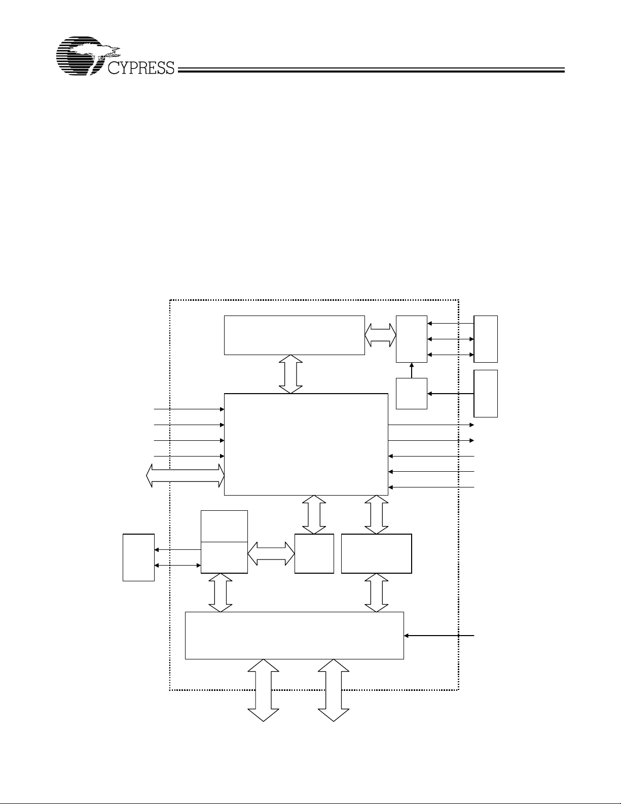
1.4 Functional Block Diagram
USB HS/FS
Control Logic
USB
2.0
Xcvr
BUS
D+
D-
USB
256 Byte
EEPROM
nEJECT
SYSIRQ
DRVPWRVLD
DISKRDY
GPIO Pins (3)
SCL
SD
ROM
EEPROM
Interface
Control
CY7C68310
Control Logic
Control
64 Byte
RAM
ATA Interface Logic
Bulk
2kByte FIFO
OSC
LOWPWR
nPWR500
BUSPWRVLD
BUSPWRD
nRESET
TAEN
Xtal
30MHz
ATA Control
16-bit Data
Figure 1-1. Block Diagram
Document #: 38-08030 Rev. *G Page 5 of 38
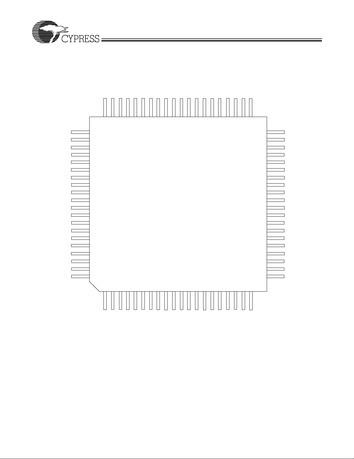
2.0 Pin Assignments
2.1 Pin Diagram
CY7C68310
VDD33 VDD25
nDIOW
nDIOR
IORDY
ATAPUEN
nDMACK
ATAIRQ
DA1
VDD33
DA0
DA2
nCS0
nCS1
nPWR500
SCL
SDA_nIMODE
DISKRDY
VBUSPWRD
VBUSPWRVLD
VDD25
61
62
63
64
65
66
67
68
69
70
71
72
73
74
75
76
77
78
79
80
60
VSS
VDD25
DMARQ
DD15
DD0
DD14
DD1
DD13
57
56
55
59
58
54
53
52
CY7C68310-80AC
VDD33
DD2
DD12
51
50
49
VSS
DD4
DD10
45
44
DD5
43
DD3
DD11
48
47
46
DD8
DD9
DD6
42
41
40
39
38
37
36
35
34
33
32
31
30
29
28
27
26
25
24
23
22
21
DD7
TMC2
TMC1
nATARST
nRESET
LOWPWR
SCANEN
GPIO2_nHS
GPIO1
GPIO0
ATAEN
DRVPWRVLD
SYSIRQ
nEJECT
TEST3
VDD33
XO
XI
VSS
4
5
1
2
3
VSS
RPU
VDD25
6
7
DP
VSS
RSDP
VDD33
8
DM
9
RSDM
10
VSS
11
PVDD25
12
13
14
15
16
AVS S
RREF
AVS S
AVS S
AVD D25
17
18
VDD25
TEST0
19
TEST1
20
TEST2
Figure 2-1. 80-pin TQFP
Document #: 38-08030 Rev. *G Page 6 of 38

CY7C68310
2.2 Pin Overview
Pin
Number Pin Name
2 RPU O USB Output D+ pull-up source. Power source for 1.5k pull-up resistor attached
5 RSDP O USB I/O USB full-speed output buffer (D+). RSDP also functions as a
6 DP I/O USB I/O USB high-speed I/O buffer (D+).
8 DM I/O USB I/O USB high-speed I/O buffer (D-).
9 RSDM O USB I/O USB full-speed output buffer (D-). RSDM also functions as a
18–20, 25 TEST[0:3] I 5V-tolerant input
22 XI I OSC input
23 XO O OSC output 30-MHz crystal output.
26 nEJECT I 5V-tolerant
27 SYSIRQ I 5V-tolerant
28 DRVPWRVLD I 5V-tolerant
29 ATAEN I 5V-tolerant
30–32 GPIO[0:1],
GPIO2_nHS
33 SCANEN I 5V tolerant
34 LOWPWR O high-Z driver,
35 nRESET I 5V-tolerant
36 nATARST O 3.3V drive,
37, 38 TMC[1:2] I 3.3V input Active HIGH. ASIC test pins. These pins must be tied to GND during
56, 54, 52,
DD[0:15] I/O 3.3V drive,
49,46, 44,
42, 39, 41,
43, 45, 48,
51, 53, 55,
57
58 DMARQ I 5V tolerant
62 nDIOW O 3.3V drive,
Pin
Direction Pin Type Pin Description
to D+ during full-speed operation.
current sink for termination during high-speed operation.
current sink for termination during high-speed operation.
Active HIGH. ASIC fabrication and manufacturing test mode select.
buffer
These pins must be tied to GND during normal operation.
30-MHz crystal input.
(2.5V-tolerant)
Active LOW. Media eject or remote wakeup requested. Tie to +3.3V
Schmitt input
if functionality is not used.
Active HIGH. USB interrupt request. Tie to GND if functionality is not
Schmitt input
used.
Configurable polarity. Device Presence Detect. This pin must not
Schmitt input
be allowed to float if functionality is not utilized.
Active HIGH. ATA interface enable.
Schmitt input
‘1’ = normal ATA operation
‘0’ = High-Z ATA interface pins and ATA interface logic halted
I/O 3.3V drive,
5V-tolerant,
6-mA IOL,
Schmitt input
General purpose I/O pins. The GPIO pins must be tied to GND if
functionality is not utilized. If the hs_indicator config bit is set, the
GPIO2_nHS pin will reflect the operating speed of the device.
‘1’ = full-speed operation
‘0’ = high-speed operation
Active HIGH. ASIC test pin. This pin must be tied to GND during
input buffer
normal operation.
Active HIGH. USB suspend indicator.
5V-tolerant,
6-mA I
OL
‘0’ = Chip active. VBUS power up to 100 mA granted.
‘High-Z’ = Chip suspend. VBUS system current limited to USB
suspend mode value.
Active LOW. Asynchronous chip reset.
Schmitt input
Active LOW. ATA reset signal.
5V-tolerant,
6-mA I
OL
normal operation.
ATA data signals.
5V-tolerant,
OL
,
6-mA I
Schmitt input
ATA control signal.
Schmitt input
ATA control signal.
5V-tolerant,
6-mA I
OL
Document #: 38-08030 Rev. *G Page 7 of 38

CY7C68310
2.2 Pin Overview (continued)
Pin
Number Pin Name
63 nDIOR O 3.3V drive,
64 IORDY I 5V-tolerant
65 ATAPUEN O 3.3V drive,
66 nDMACK O 3.3V drive,
67 ATA IRQ I 5V-tolerant
70, 68, 71 DA[0:2] O 3.3V drive,
72, 73 nCS[0:1] O 3.3V drive,
74 nPWR500 O high-Z driver,
75 SCL O high-Z driver,
76 SDA_nlMODE I/O high-Z driver,
77 DISKRDY I 5V-tolerant
78 VBUSPWRD I 5V-tolerant
79 VBUSPWRVLD I 5V-tolerant
1, 4, 10,
VSS Power Digital ground.
21, 47, 60
3, 17, 40,
VDD25 Power 2.5V digital supply.
59, 80
7, 24, 50,
VDD33 Power 3.3V digital supply.
61, 69
11 PVDD25 Power Analog 2.5V supply (PLL).
12,14,16 AVSS Power Analog ground.
13 RREF Power PLL voltage reference. Current source for 2.4k (1%) resistor
15 AVDD25 Power Analog 2.5V supply.
Pin
Direction Pin Type Pin Description
ATA control signal.
5V-tolerant,
6 mA I
OL
ATA control signal.
Schmitt input
ATA IORDY pull-up connection. For VBUS-powered systems.
5V-tolerant,
6 mA I
OL
ATA control signal.
5V-tolerant,
6 mA I
OL
ATA interrupt request.
Schmitt input
ATA address signals.
5V-tolerant,
6 mA I
OL
ATA chip select signals.
5V-tolerant,
6 mA I
OL
Active LOW. VBUS power granted indicator.
5V-tolerant,
6 mA I
OL
5V-tolerant,
6 mA I
OL
‘0’ = VBUS power up to bMaxPower value
‘high-Z’ = bMaxPower value not granted (if more than 100 mA)
I2C-compatible clock. This pin may be left as a no-connect pin if
2
C-compatible interface is not utilized.
the I
I2C-compatible address/data or nIMODE select.
5V-tolerant,
6 mA I
Schmitt input
OL
,
Configurable polarity. Device ready.
Schmitt input
Active HIGH. Bus-powered operation select pin.
Schmitt input
‘1’ = Bus powered
‘0’ = Self powered
Active HIGH. Indicates that VBUS power is present.
Schmitt input
connected to AVSS.
Document #: 38-08030 Rev. *G Page 8 of 38

CY7C68310
2.3 Detailed Pin Descriptions
2.3.1 DP, DM
DP and DM are the high-speed USB signaling pins, and they should be tied to the D+ and D– pins of the USB connector. Because
they operate at high frequencies, the USB signals require special consideration when designing the layout of the PCB. See section
13.0 for PCB layout guidelines.
2.3.2 RSDP, RSDM
RSDP and RSDM are the full-speed USB signaling pins, and they should be tied to the DP and DM pins through 39Ω resistors.
RSDP and RSDM also function as current sinks for termination during high-speed operation.
2.3.3 TEST[0:3]
The test pins control the various test modes of the CY7C68310. Most test modes are reserved for ASIC fabrication, but the
following table outlines the test modes available for device manufacturing environments. The test pins must be tied to GND for
normal operation.
Table 2-1. CY7C68310 Test Modes
Test Mode Description
0000 Normal Mode. This is the default mode of operation.
0001 Reserved.
0010 Limbo Mode. All output pins set to high-Z during Limbo mode operation with the exception of the XO pin. The XO
pin output cell does not have high-Z control (always enabled), and must be disabled or disconnected by other
means. To enter Limbo Mode, nRESET must be toggled after the Test pins are set to ‘0010’.
0011 Input xnorTree Mode. This mode tests the connectivity of all dedicated inputs and outputs. While in the Input
0100 Bi-di xnorTree Mode. This mode test the connectivity of all bi-directional inputs. While in the Bi-di xnor Tree Mode
0101–1111 Reserved.
xnorTree Mode of operation, all bi-directional pins are wired as chain outputs. The results of the connectivity
procedure will be seen on all bidirectional pins. Chain Inputs (in order): VBUSPWRVLD, VBUSPWRD, DISKRDY,
ATAIRQ, IORDY, DMARQ, nRESET, ATAEN, DRVPWRVLD, SYSIRQ, nEJECT Chain Outputs (in order):
GPIO[2:0], DD[15:0], SDA_nIMODE.
of operation, all bi-directional pins are wired as inputs and become part of the xnor Tree chain. The results of the
connectivity procedure will be seen on all output only pins. Chain Inputs: GPIO[0], GPIO[1], GPIO[2], DD[7], DD[8],
DD[6], DD[0], DD[5], DD[10], DD[4], DD[11], DD[3], DD[12], DD[2], DD[13], DD[1], DD[14], DD[0], DD[15],
SDA_nIMODE. Chain Outputs: nPWR500, nATARST, nDIOW, nDIOR, nDMACK, ATAPUEN, nCS[1:0], DA[2:0],
LOWPWR, SCL
2.3.4 XI, XO
The CY7C68310 requires a 30-MHz signal to derive internal timing. Typically a 30-MHz (2.5V tolerant, parallel-resonant fundamental mode) crystal is used, but a 30-MHz (2.5V, 50% duty cycle) square wave from another source can also be used. If a crystal
is used, connect the pins to XI and XO, and also through 20pF capacitors to GND as shown in Figure 6-1. If an alternate clock
source is used, apply it to XI and leave XO open.
2.3.5 nEJECT
The nEJECT input pin provides a means to communicate an Eject button push to the ATA/ATAPI device via event notification as
well as a way to cause a USB Remote-wakeup. During normal operation, asserting nEJECT for 10ms indicates that a media eject
has been requested. If the CY7C68310 is in a suspend state, and if remote wakeup is enabled by the USB host, a state change
on this pin will immediately cause the CY7C68310 to perform a USB remote wakeup event.
2.3.6 SYSIRQ
The SYSIRQ pin provides a way for systems to request service from host software by use of the USB Interrupt pipe. If the
CY7C68310 has no pending interrupt data to return, USB interrupt pipe data requests are NAKed. If pending data is available,
CY7C68310 returns 16 bits of data indicating the state of the DISKRDY pin, the HS_MODE signal (that indicates whether
CY7C68310 is operating in high-speed or full-speed), the VBUSPWRD pin, the User-Defined values from bits [7:3] of address
0xE of the configuration space, and the GPIO Pins. Tab le 2-2 shows the bitmap for the data returned on the interrupt pipe, and
the figure beneath it depicts the latching algorithm incorporated by CY7C68310.
Document #: 38-08030 Rev. *G Page 9 of 38
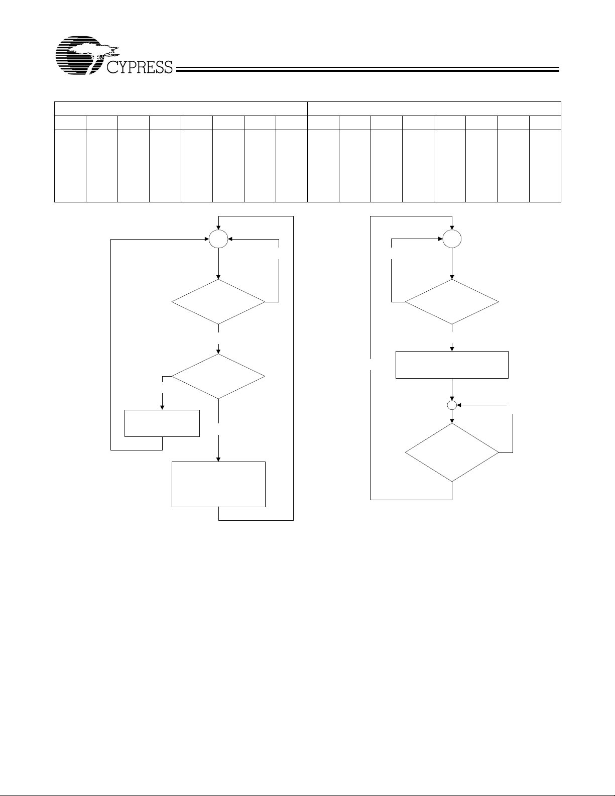
CY7C68310
Table 2-2. USB Interrupt Pipe Data Bitmap
USB Interrupt Data Byte 1 USB Interrupt Data Byte 0
7654321076543210
0
0
0
0
0
DISKRDY
USB High-Speed
VBUSPWRD
USER_DEF[4]
USER_DEF[3]
USER_DEF[2]
USER_DEF[1]
USER_DEF[0]
GPIO[2]
GPIO[1]
GPIO[0]
Yes
No
SYSIRQ=1?
Yes
Latch State of IO Pins
Set Int_Data = 1
No
Int_Data = 0
and
SYSIRQ=0?
No
NAK Request
Return Interrupt Data
No
USB Interrupt
Pipe Polled?
Yes
Int_Data = 1?
Yes
Set Int_Data = 0
Figure 2-2. SYSIRQ Latching Algorithm
2.3.7 DRVPWRVLD
DRVPWRVLD can be used with removable devices (such as compact flash) to indicate that the media device is present. Pin
polarity and function enable are controlled by bits 4 and 2, respectively, of EEPROM address 0x0B. When DRVPWRVLD is
deasserted, the CY7C68310 will remove the pull-up on D+ (causing the CY7C68310 to drop off the USB), suspend all ATA state
machine activity, drive all ATA interface signals to ‘0’ (assuming ATAEN = ‘1’), and enter into a low-power state. The CY7C68310
will remain in this state until DRVPWRVLD is asserted, at which time it will enable the D+ pull-up, allow resume of ATA state
machine activity, and begin to drive the ATA interface pins (assuming ATAEN = ‘1’).
2.3.8 ATAEN
The ATAEN pin allows ATA bus sharing with other host devices. Deasserting ATAEN causes the CY7C68310 to high-Z all ATA
bus interface pins and suspend ATA state machine activity, otherwise leaving the CY7C68310 operational (USB operation
continues). Asserting ATAEN causes the CY7C68310 to reset the drive and resume normal operation. To disable USB operation
and the ATA interface, the DRVPWRVLD signal can be used in conjunction with ATAEN to force the CY7C68310 into a low-power
state until normal operation is resumed. Note that disabling the ATA bus with the ATAEN pin during the middle of a data transfer
will result in data loss and may cause the operating system on the host computer to crash.
Document #: 38-08030 Rev. *G Page 10 of 38

CY7C68310
2.3.9 GPIO Pins
The GPIO pins allow for a general purpose Input/Output interface. Configuration bytes 0x0E and 0x0F contain the settings for
the GPIO pins. See section 4.3 for details of how to use the vendor-specific commands to utilize the GPIO functionality. The status
of the GPIO pins is also returned by a USB interrupt event. See section 2.3.6 for SYSIRQ details. Alternatively, if the hs_indicator
config bit is set (bit 4 of EEPROM address 0x0F), the GPIO2_nHS pin will reflect the operating speed of the device.
2.3.10 LOWPWR
LOWPWR is an output pin that, when in a high-Z state, indicates that the CY7C68310 is in a suspend state. When LOWPWR
output is driven ‘0’, the CY7C68310 is active.
2.3.11 nRESET
Asserting nRESET for a minimum of 1 ms after power rails are stable will reset the entire chip. An RC reset circuit should be used
that ensures that no spurious resets occur.
2.3.12 ATAPUEN
This output provides control for the required host pull-up resistors on the ATA interface. ATAPUEN is driven ‘0’ when the ATA bus
is inactive. ATAPUEN is driven ‘1’ when ATA bus is active. ATAPUEN is set to a high-Z state along with all other ATA interface
pins when ATAEN is deasserted.
2.3.13 nPWR500
nPWR500 is an external pin that, when asserted, indicates VBUS current may be drawn up to the limit specified by the bMaxPower
field of the USB configuration descriptors. nPWR500 will only be asserted if VBUSPWRD is also asserted. If the CY7C68310
enters a low-power state, nPWR500 is deasserted. When normal operation is resumed, nPWR500 is restored accordingly. The
nPWR500 pin should never be used to control power sources for the CY7C68310.
2.3.14 SCL, SDA_nIMODE
If an external EEPROM device is used to store configuration information, the clock and data pins for the I
should be connected to the configuration EEPROM and to VCC through 2.2kΩ resistors as shown in Figure 6-1. If configuration
information is to be obtained from the attached ATA/ATAPI device (IMODE), SCL should be left as a no-connect and
SDA_nIMODE should be tied to GND.
2
C-compatible port
2.3.15 DISKRDY
This input pin indicates the attached device is powered and ready to begin communication with the CY7C68310. DISKRDY
polarity can be set using EEPROM address 0x05, bit 0. DISKRDY qualifies the start of the CY7C68310 initialization sequence.
A state change from ‘0’ to ‘1’ on DISKRDY will cause the CY7C68310 to wait for 25 ms before asserting nATARESET and reinitializing the device. The ATA interface state machines remain inactive and all of the ATA interface signals are driven logic '0' if
DISKRDY is not asserted (assuming ATAEN = '1'). DISKRDY is filtered for 25 ms on the asserting edge and cleared asynchronously on the deasserting edge.
2.3.16 VBUSPWRD
The VBUSPWRD input pin indicates whether the device will report itself as bus-powered or self-powered. VBUSPWRD also
qualifies the use of nPWR500. Based upon the state of this pin at start-up, the CY7C68310 will request the amount of current
specified in the bMaxPower field of the USB Configuration Descriptor. If VBUSPWRD is asserted, the CY7C68310 will report that
the device is bus-powered. If VBUSPWRD is deasserted, the CY7C68310 will report that the device is self-powered.
2.3.17 VBUSPWRVLD
VBUSPWRVLD (USB VBUS Power Valid) indicates that VBUS power is present at the USB connector. VBUSPWRVLD qualifies
driving the system’s 1.5KΩ pull-up resistor on D+ (the USB specification only allows the device to source power to D+ when the
host is powered). VBUSPWRVLD is conditioned so that it is only detected after valid chip configuration bits have been loaded.
3.0 Functional Overview
3.1 USB Signaling Speeds
The CY7C68310 operates at two of the three signal rates that are defined in the Universal Serial Bus Specification Revision 2.0:
• Full-speed, with a signaling bit rate of 12 Mbits/sec.
• High-speed, with a signaling bit rate of 480 Mbits/sec.
Document #: 38-08030 Rev. *G Page 11 of 38

CY7C68310
3.2 ATA Interface
The ATA/ATAPI port on the CY7C68310 is compliant with the Information Technology–AT Attachment with Packet Interface–6
(ATA/ATAPI-6) Specification, T13/1410D Rev 2a. The CY7C68310 supports both ATAPI packet commands as well as ATA
commands (by use of ATA Command Blocks), as outlined in Sections 3.2.1 and 3.2.2. Refer to the USB Mass Storage Class
(MSC) Bulk Only Transport Specification for information on Command Block formatting. Additionally, the CY7C68310 translates
ATAPI SFF-8070i commands to ATA commands for seamless integration of ATA devices with generic Mass Storage Class BOT
drivers. The CY7C68310 also provides a vendor-specific “event notify” ATA command to automatically communicate certain USB
and system events to the attached device.
3.2.1 ATA Command Block (ATACB)
The ATA Command Block (ATACB) functionality provides a means of passing ATA commands and ATA register accesses for
execution. ATACB commands are transferred in the Command Block Wrapper Command Block (CBWCB) portion of the
Command Block Wrapper (CBW). The ATACB is distinguished from other command blocks by the first two bytes of the command
block matching the wATACBSignature. Only command blocks that have a valid wATACBSignature are interpreted as ATA
Command Blocks. All other fields of the CBW and restrictions on the CBWCB remain as defined in the USB Mass Storage Class
Bulk-Only Transport Specification. The ATACB must be 16 bytes in length. The following table and text defines the fields of the
ATACB.
Table 3-1. ATACB Field Descriptions
Byte Field Name Field Description
0 bVSCBSignature This field indicates to the CY7C68310 that the ATACB contains a vendor-
1 bVSCBSubCommand This field must be set to 0x024h for ATACB commands.
2 bmATACBActionSelect This field controls the execution of the ATACB according to the bitfield values:
specific command block. This value of this filed must match the value in
EEPROM address 0x06h for this vendor-specific command to be recognized.
Bit 7 IdentifyPacketDevice - This bit indicates that the data phase of the
command will contain ATAPI (0xA1h) or ATA (0xECh) IDENTIFY device data.
Setting IdentifyPacketDevice when the data phase does not contain IDENTIFY
device data will result in unspecified device behavior.
0 = Data phase does not contain IDENTIFY device data
1= Data phase contains ATAPI or ATA IDENTIFY device data
Bit 6 UDMACommand - This bit enables supported UDMA device transfers.
Setting this bit when a non-UDMA capable device is attached will result in
undetermined behavior.
0 = Do not use UDMA device transfers (only use PIO mode)
1= Use UDMA device transfers
Bit 5 DEVOverride - This bit determines whether the DEV bit value is taken
from the CY7C68310 configuration data or from the ATACB.
0 = The DEV bit will be taken from EEPROM address 0x05h, bit 5
1= The DEV bit will be taken from the ATACB field 0x0B, bit 4
Bit 4:3 DPErrorOverride - These bits control the Device and Phase Error
override feature. These bits shall not be set in conjunction with bmATACBTaskFileRead.
00 = Data accesses are halted if a device or phase error is detected
01 = Data accesses are halted if a device error is detected, but not a phase error
10 = Data accesses are halted if a phase error is detected, but not a device error
11 = Neither device or phase errors will result in halting of data accesses
Bit 2 PollAltStatOverride - This bit determines whether or not the Alternate
Status register will be polled and the BSY bit will be used to qualify the start of
ATACB operation.
0 = The AltStat register will be polled until BSY=0 before proceeding with the
ATACB operation
1= The ATACB operation will be executed without polling the AltStat register
Bit 1 DeviceSelectionOverride - This bit determines when the device selection
will be performed in relation to the command register write accesses.
0 = Device selection will be performed prior to command register write
accesses
1 = Device selection will be performed following command register write
accesses
Document #: 38-08030 Rev. *G Page 12 of 38

CY7C68310
Table 3-1. ATACB Field Descriptions
Byte Field Name Field Description
Bit 0 TaskFileRead - This bit determines whether or not the taskfile register
data selected in bmATACBRegisterSelect is returned. If this bit is set, the
dCBWDataTransferLength field must be set to 8.
0 = Execute ATACB command and data transfer (if any)
1 = Only read taskfile registers selected in bmATACBRegisterSelect and return
0x00h for all others. The format of the 8 bytes of returned data is as follows:
• Address offset 0x00 (3F6h) - Alternate Status
• Address offset 0x01 (1F1h) - Features / Error
• Address offset 0x02 (1F2h) - Sector Count
• Address offset 0x03 (1F3h) - Sector Number
• Address offset 0x04 (1F4h) - Cylinder Low
• Address offset 0x05 (1F5h) - Cylinder High
• Address offset 0x06 (1F6h) - Device / Head
• Address offset 0x07 (1F7h) - Command / Status
3 bmATACBRegisterSelect This field controls which of the taskfile register read or write accesses occur.
Taskfile read data will always be 8 bytes in length, and unselected register data
will be returned as 0x00h. Register accesses occur in sequential order as
outlined below (0 to 7):
Bit 0 (3F6h) Device Control / Alternate Status
Bit 1 (1F1h) Features / Error
Bit 2 (1F2h) Sector Count
Bit 3 (1F3h) Sector Number
Bit 4 (1F4h) Cylinder Low
Bit 5 (1F5h) Cylinder High
Bit 6 (1F6h) Device / Head
Bit 7 (1F7h) Command / Status
4 bATACBTransferBlockCount This value indicates the maximum requested block size in 512-byte incre-
ments. This value must be set to the last value used for the “Sectors per block”
in the SET_MULTIPLE_MODE command. Legal values are 0, 1, 2, 4, 8, 16,
32, 64, and 128 where 0 indicates 256 sectors per block. A command failed
status will be returned if an illegal value is used in the ATACB.
5-12 bATACBTaskFileWriteData These bytes contain ATA register data used with ATA command or PIO write
operations. Only registers selected in bmATACBRegisterSelect are required to
hold valid data when accessed. The registers are as follows:
• ATACB Address Offset 0x05h (3F6h) - Device Control
• ATACB Address Offset 0x06h (1F1h) - Features
• ATACB Address Offset 0x07h (1F2h) - Sector Count
• ATACB Address Offset 0x08h (1F3h) - Sector Number
• ATACB Address Offset 0x09h (1F4h) - Cylinder Low
• ATACB Address Offset 0x0Ah (1F5h) - Cylinder High
• ATACB Address Offset 0x0Bh (1F6h) - Device
• ATACB Address Offset 0x0Ch (1F7h) - Command
13-15 Reserved These bytes must be set to 0x00h for ATACB commands.
Document #: 38-08030 Rev. *G Page 13 of 38

CY7C68310
3.2.2 ATA Command Block 2 (ATACB2)
The ATA Command Block 2 (ATACB2) functionality provides a means of passing ATA commands and ATA register accesses for
execution. ATACB2 allows for 48-bit commands. ATACB2 commands are transferred in the CBWCB portion of the CBW. The
ATACB2 is distinguished from other command blocks by the first two bytes of the command block matching the
wATACB2Signature. Only command blocks that have a valid wATACB2Signature are interpreted as ATACB2 commands. All other
fields of the CBW and restrictions on the CBWCB shall remain as defined in the USB Mass Storage Class Bulk-Only Transport
Specification. The ATACB2 must be 16 bytes in length. The following table and text defines the fields of the ATACB2.
Table 3-2. ATACB2 Field Descriptions
Byte Field Name Field Description
0 bVSCBSignature This field indicates to the CY7C68310 that the ATACB contains a vendor-
specific command block. This value of this filed must match the value in
EEPROM address 0x06h for this vendor-specific command to be recognized.
1 bVSCBSubCommand This field must be set to 0x025h for ATACB2 commands.
2 bmATACB2RegisterSelect This field controls which of the taskfile register read or write accesses occur.
Taskfile read data will always be 12 bytes in length, and unselected register data
will be returned as 0x00h. Register accesses occur in sequential order as
outlined below (0 to 7):
Bit 0 (3F6h) - Alternate Status (read only, unaffected by write commands)
Bit 1 (1F1h) - Features / Error
Bit 2 (1F2h) - Sector Count
Bit 3 (1F3h) - LBA Low (Sector Number)
Bit 4 (1F4h) - LBA Mid (Cylinder Low)
Bit 5 (1F5h) - LBA High (Cylinder High)
Bit 6 (1F6h) - Device / Head (see bmATACB2ActionSelect1)
Bit 7 (1F7h) - Command / Status
3 bmATACB2ActionSelect1 This field controls the execution of the ATACB2 according to the bitfield values:
Bit 7 IdentifyDevice - This bit indicates that the data phase of the command will
contain ATAPI (0xA1h) or ATA (0xECh) IDENTIFY device data. Setting IdentifyDevice when the data phase does not contain IDENTIFY device data will result
in undetermined device behavior.
0 = Data phase does not contain IDENTIFY device data
1= Data phase contains ATAPI or ATA IDENTIFY device data
Bit 6 UDMACommand - This bit enables supported UDMA device transfers.
Setting this bit when a non-UDMA capable device is attached will result in
undetermined behavior.
0 = Do not use UDMA device transfers (only use PIO mode)
1= Use UDMA device transfers
Bit 5 DEVOverride - This bit determines whether the DEV bit value is taken from
the CY7C68310 configuration data or from the ATACB2.
0 = The DEV bit will be taken from EEPROM address 0x05h, bit 5
1= The DEV bit will be taken from bATACB2DeviceHeadData[5]
Bit 4 DErrorOverride - This bit controls the device error override feature. This
bit should not be set during a bmATACB2ActionSelect TaskFileRead.
0 = Data accesses are halted if a device error is detected
1 = Data accesses are not halted if a device error is detected
Bit 3 PErrorOverride - This bit controls the phase error override feature. This bit
should not be set during a bmATACB2ActionSelect TaskFileRead.
0 = Data accesses are halted if a phase error is detected
1 = Data accesses are not halted if a phase error is detected
Bit 2 PollAltStatOverride - This bit determines whether or not the Alternate Status
register will be polled and its BSY bit will be used to qualify the start of ATACB
operation.
0 = The AltStat register will be polled until BSY=0 before proceeding with the
ATACB operation
1= The ATACB operation will be executed without polling the AltStat register
Document #: 38-08030 Rev. *G Page 14 of 38

CY7C68310
Table 3-2. ATACB2 Field Descriptions
Byte Field Name Field Description
Bit 1 DeviceSelectionOverride - This bit determines when the device selection
will be performed in relation to the command register write accesses.
0 = Device selection will be performed prior to command register accesses
1 = Device selection will be performed following command register accesses
Bit 0 Task Fil eR ead - This bit determines whether or not the taskfile register data
selected in bmATACB2RegisterSelect is returned. If this bit is set, the
dCBWDataTransferLength field must be set to 12.
0 = Execute ATACB2 command and data transfer (if any)
1 = Only read taskfile registers selected in bmATACBRegisterSelect and return
0x00h for all others. The format of the 12 bytes of returned data is as follows:
• Address offset 0x00h (3F6h) Alternate Status (HOB=0)
• Address offset 0x01h (1F6h) Device / Head (HOB=0)
• Address offset 0x02h (1F1h) Error (HOB=0)
• Address offset 0x03h (1F2h-M) Sector Count (HOB=1)
• Address offset 0x04h (1F3h-M) LBA Low (Sector Number) (HOB=1)
• Address offset 0x05h (1F4h-M) LBA Mid (Cylinder Low) (HOB=1)
• Address offset 0x06h (1F5h-M) LBA High (Cylinder High) (HOB=1)
• Address offset 0x07h (1F2h-L) Sector Count (HOB=0)
• Address offset 0x08h (1F3h-L) LBA Low (HOB=0)
• Address offset 0x09h (1F4h-L) LBA Mid (HOB=0)
• Address offset 0x0Ah (1F5h-L) LBA High (HOB=0)
• Address offset 0x0Bh (1F7h) Status (HOB=0)
4 bATACB2TransferBlockCount[7:4] These bits indicate the DRQ block size in 512-byte increments. This value is log
bmATACB2ActionSelect2[3:0] This field controls the execution of the ATACB according to the bitfield values:
5 bATACB2DeviceHeadData The contents of this field are used for writing the Device Head register when
6-15 bATACB2TaskFileWriteData These bytes contain ATA register data used with ATA command or PIO write
base 2 of the block size. Legal values are 0 (1 sector per block) through 8 (256
sectors per block). A command failed status will be returned if an illegal value
is used in the ATACB2. For commands using multiple sector PIO data transfers,
the number of sectors per block must equal the current Multiple Sector Setting
of the drive. These bits should be set to ‘0’ for non-multiple, non-UDMA
commands.
Bits 3-1 Reserved - These bits must be set to ‘0’
Bit 0 48-bit-write - Determines whether or not M data is used to read 1F2-1F5
0 = Do not read or write 1F2-1F5 with “-M” data
1 = Read or write 1F2-1F5 with “-M” data
Byte 2, Bit 6 of the ATACB2 is set to ‘1’. Otherwise, the value written will be
determined by the bridge.
Bits 7-5 DevHead - Data used to write to Device Head register.
Bit 4 DEVOverride - This bit reflects the state of Byte 3, Bit 5 of the ATACB2.
Bits 3-0 DevHead - Data used to write to Device head register.
operations. Only registers selected in bmATACB2RegisterSelect are required
to hold valid data when accessed. The registers are as follows:
• ATACB2 Address offset 6h (1F1h) Features
• ATACB2 Address offset 7h (1F2h-M) Sector Count
• ATACB2 Address offset 8h (1F3h-M) LBA Low (Sector Number)
• ATACB2 Address offset 9h(1F4h-M) LBA Mid (Cylinder Low)
• ATACB2 Address offset Ah (1F5h-M) LBA High (Cylinder High)
• ATACB2 Address offset Bh (1F2h-L) Sector Count
• ATACB2 Address offset Ch (1F3h-L) LBA Low
• ATACB2 Address offset Dh (1F4h-L) LBA Mid
• ATACB2 Address offset Eh (1F5h-L) LBA High
• ATACB2 Address offset Fh (1F7h) Command
Document #: 38-08030 Rev. *G Page 15 of 38

CY7C68310
3.2.3 Vendor-specific EVENT_NOTIFY Command
The vendor-specific EVENT_NOTIFY command enables the CY7C68310 to communicate the occurrence of certain USB and
system events to the attached device if the device’s firmware supports the EVENT_NOTIFY command. The command code is
specified by configuration address 0x02. Setting this byte to 0x00 disables the EVENT_NOTIFY feature.
Table 3-3. Notification Register Read Values
Register 7 6 5 4 3 2 1 0
Error N/A
Sector Count N/A
LBA Low (Sector Number) N/A
LBA Mid (Cylinder Low) nSTATE0
LBA High (Cylinder High) nSTATE1
Device/Head N/A
Status BUSY N/A N/A N/A DRQ N/A N/A N/A
The nSTATE0 and nSTATE1 values are read from the device and stored for use as the STATE0 and STATE1 values during the
next execution of the event notification command. The nSTATE0 and nSTATE1 values provide temporary non-volatile storage for
devices whose power is controlled by nPWR500 (typically bus-powered systems). This allows the device to store information
prior to entering a USB Suspend state for retrieval after resuming from the USB Suspend state. Note that a USB Reset from the
host may interrupt the collection of data. The device must accommodate the potential for this occurrence. The BSY and DRQ bits
must be cleared by the device upon the completion of an event notification command.
Table 3-4. Notification Register Write Values
Register 7 6 5 4 3 2 1 0
Features
Sector Count Reserved Reserved Reserved Reserved
LBA Low (Sector Number) N/A
LBA Mid (Cylinder Low) STATE0
LBA High (Cylinder High) STATE1
Device/Head N/A
Command Specified in Configuration byte 0x02
USB
Reset
Class
Specific
Reset
USB
Suspend
USB
Resume
Reserved Reserved
Self-
Powered
Bus-
Powered
Eject Button
Pressed
USB
High-Speed
Eject
Button
Released
USB
Full-Speed
The STATE0 and STATE1 values are written with the value of nSTATE0 and nSTATE1 obtained from the previously completed
event notification command. Assertion of nRESET resets STATE0 and STATE1 to 0x00.
4.0 Configuration
Certain timing parameters and operational modes for the CY7C68310 are configurable. Some USB configuration and descriptor
values are also configurable. CY7C68310 configuration data should not be confused with the USB Configuration Descriptor data.
4.1 CY7C68310 Configuration and USB Descriptor Sources
CY7C68310 configuration and USB descriptor data can be retrieved from three sources. Table 4-1 indicates the method of
determining which data source is used.
Document #: 38-08030 Rev. *G Page 16 of 38

CY7C68310
Table 4-1. CY7C68310 Configuration and USB Descriptor Sources
2
C-compatible
I
SDA_nIMODE = 0
Device Present
No No N/A In this mode, the CY7C68310 uses internal ROM contents for USB
Yes N/A No In this mode, the CY7C68310 uses internal ROM contents for USB
Yes N/A Yes The CY7C68310 retrieves all Descriptor and Configuration values from
No Yes No The CY7C68310 uses internal ROM contents for USB descriptor infor-
No Yes Yes The CY7C68310 retrieves all Descriptor and Configuration values from
4.1.1 I
2
C-compatible Device
The CY7C68310 provides support for the 24LCXXB family of EEPROMs. Following the release of nRESET, the CY7C68310
waits 50 ms and then checks for I
signature check, the CY7C68310 re-tests the signature with each vendor-specific USB load or read access of configuration bytes
0 and 1. Once the signature check passes, I2C-compatible data is returned for USB descriptor requests. If an I2C-compatible
device is detected initially, it is always assumed present until the next reset cycle (nRESET). If an I
present, a lack of an ACK response when required causes the CY7C68310 to stall that USB request. The CY7C68310 will attempt
the access again with the next USB request.
I2C Signature
Check Passes CY7C68310 Configuration and USB Descriptor Retrieval Method
descriptor information and configuration register values. This mode is
for debug/manufacturing operation only. Not for shipping products.
descriptor information. Configuration register values are loaded from
internal ROM. This is not a valid mode of operation.
the vendor-specific Identify (FBh) data. The CY7C68310 is configured
using internal ROM values until FBh data becomes available.
mation. Configuration register values are loaded from internal ROM. In
this mode of operation, any CY7C68310 vendor-specific configuration
access causes the CY7C68310 to recheck the signature field. Once
the signature check passes, SROM data is returned for USB
descriptors requests. This is not a valid mode of operation.
2
the I
C-compatible memory device. The CY7C68310 is configured
using these values.
2
C-compatible device presence. If an I2C-compatible device is present but does not pass
2
C-compatible device is
4.1.2 IMODE
Configuration and descriptor data can also be supplied by an attached mass storage device (IMODE) through a vendor-specific
Identify (FBh) ATA command. The CY7C68310 provides 256 bytes of internal RAM for FBh data storage. Unlike operation with
an external I2C-compatible memory device, IMODE operation requires the attached device first be initialized and FBh data
retrieved before the CY7C68310 can allow USB enumeration. To meet USB specification requirements, IMODE operation must
be limited to systems that draw 100 mA or less from VBUS prior to USB configuration.
4.1.3 Internal ROM Contents
The CY7C68310 also contains an internal set of CY7C68310 configuration and USB descriptors. The internal descriptors may
only be used during manufacturing, as the internal ROM values disable some features required for normal operation to aid use
in a manufacturing environment. Also, the internal ROM descriptors do not provide a unique serial number (required for USB
Mass Storage Class compliance), and therefore cannot be used for shipping products. See Ta bl e 4- 2 for the organization of the
internal ROM contents. An external I
2
C-compatible memory device or utilization of the vendor-specific FBh identify command is
required to correctly configure the CY7C68310 for operation and provide a unique serial number for MSC compliance.
4.2 EEPROM Organization
CY7C68310 configuration and USB descriptor data can be supplied from an I2C-compatible serial memory device. The
CY7C68310 can address 2 Kbytes of I
limited to 512 bytes maximum. Unused register space in the I
specific data storage. Note that no descriptor is allowed to span multiple pages within the I
2
C-compatible data, but CY7C68310 configuration and USB descriptor information are
2
C-compatible serial memory device may be used for product
2
C-compatible serial memory device.
Document #: 38-08030 Rev. *G Page 17 of 38

CY7C68310
Table 4-2. EEPROM Organization
I2C
Address Field Name Field Description
CY7C68310 Configuration Data
0x00 I
0x01 I
0x02 Event Notification Bits (7:0)
0x03 APM Value Bits (7:0)
0x04 ATA Initialization Timeout Time in 128-millisecond granularity before the CY7C68310
0x05 USB Bus Mode Bit (7) – Read only 0x00
2
C memory device Signature
(LSB)
2
C memory device Signature
(MSB)
ATAPI Command Block Size Bit (6)
Master/Slave Selection Bit (5)
ATAPI Reset Bit (4)
ATA_NATAPI Bit (3) – Read only.
Force USB FS Bit(2)
LSB I2C memory device Signature byte. 0x4B
MSB I2C memory device Signature byte. 0x50
ATAPI event notification command. The value of this register
(if other than 0x00) is used to identify the vendor-specific
Event Notification command (see Section 3.2.3). Setting this
field to 0x00 disables this feature.
ATA device Automatic Power Management value. If an
attached ATA device supports APM and this field contains
other than 0x00, the CY7C68310 will issue a SET
FEATURES command to enable APM with this register
value during the drive initialization.
stops polling the ALT STAT register for reset complete and
restarts the reset process (0x80 = 16.4 seconds).
USB bus mode of operation.
‘0’ = USB is operating in full-speed mode (12 Mbit/sec)
‘1’ = USB is operating in high-speed mode (480 Mbit/sec)
CBW Command Block Size.
‘0’ = 12 byte ATAPI CB
‘1’ = 16 byte ATAPI CB
Device number selection. This bit is valid only when “Skip
ATA/ATAPI Device Initialization” is active. Otherwise, the
value of this bit is ignored.
‘0’ = Drive 0 (master)
‘1’ = Drive 1 (slave)
ATAPI reset during drive initialization.
Setting this bit causes the CY7C68310 to issue an ATAPI
reset during device initialization.
Indicates if an ATA or ATAPI device is detected.
‘0’ = ATAPI device
‘1’ = ATA device or possible device initialization failure
Force USB full-speed only operation.
Setting this bit prevents the CY7C68310 from negotiating
HS operation during USB reset events.
‘0’ = Normal operation – allow HS negotiation during USB
reset
Required
I2C Data
Example
I2C Data
0x00
0x00
0x80
Document #: 38-08030 Rev. *G Page 18 of 38

CY7C68310
Table 4-2. EEPROM Organization (continued)
2
I
C
Address Field Name Field Description
‘1’ = USB FS only – do not allow HS negotiation during USB
reset
VS/MSC SOFT_RESET Bit(1)
Vendor-specific/MSC SOFT_RESET control.
‘0’ = Vendor-specific USB command utilized for
SOFT_RESET
‘1’ = Mass Storage Class USB command utilized for
SOFT_RESET
DISKRDY Polarity Bit (0)
DISKRDY active polarity. DISKRDY Polarity is ignored if
IMODE is set to ‘1’. During IMODE operation DISKRDY
polarity is active HIGH.
‘0’ = Active HIGH polarity
‘1’ = Active LOW polarity
0x06 ATA Command Designator Value in CBW CB field that designates if the CB is decoded
as vendor-specific ATA/CFG commands instead of the
ATAPI command block.
0x07 Reserved Bits (7:1)– must be set to ‘0’. 0x01
Retry ATAPI Bit (0)
This bit enables the CY7C68310 to accommodate ATAPI
devices that take longer to initialize than what is allowed in
the ATA/ATAPI-6 specification.
‘1’ = Retry ATAPI commands
‘0’ = Normal ATAPI timing
0x08 Initialization Status Bit (7) – Read only 0x00
Drive Initialization Status.
If set, indicates the drive initialization sequence state
machine is active.
Force ATA Device Bit (6)
Allows software to manually enable ATA Translation with
devices that do not support CY7C68310 device initialization
algorithms. Force ATA Device must be set to ‘1’ in
conjunction with Skip ATA/ATAPI Device Initialization and
ATA Translation Enable.
Skip ATA/ATAPI Device Initialization
Reserved Bits (4:3) – must be set to ‘0’.
Last LUN Identifier Bits (2:0)
0x09 ATAEN Bit (7) – Read only. 0x01
Reserved Bits (6:1) – must be set to ‘0’.
Bit (5)
Forces the CY7C68310 to skip device initialization upon
startup. This bit should be cleared for IMODE operation. The
USB device driver must initialize the attached device (if
required) when this bit is set. For ATAPI devices, the host
driver must issue an IDENTIFY command utilizing ATA.
‘0’ = normal operation
‘1’ = only reset the device and write the device control
register prior to processing commands
Maximum number of LUNs device supports.
Holds the current logic state of the ATAEN pin.
Required
I2C Data
Example
I2C Data
0x24
Document #: 38-08030 Rev. *G Page 19 of 38

CY7C68310
Table 4-2. EEPROM Organization (continued)
2
I
C
Address Field Name Field Description
SRST Enable Bit (0)
Soft-reset during drive initialization.
‘0’ = Disable soft-reset functionality
‘1’ = Enable soft-reset during drive initialization
0x0A ATA Data Assert Bits (7:4) 0x20
ATA cycle times are calculated using Data Assert and Data
Recover values.
Standard values for ATA-compliant devices and a 30.0-MHz
system clock (in binary):
mode 0 0101 (5+1)*33.33 = 200 ns
mode 1 0011 (3+1)*33.33 = 133 ns
mode 2 0011 (3+1)*33.33 = 133 ns
mode 3 0010 (2+1)*33.33 = 100 ns
mode 4 0010 (2+1)*33.33 = 100 ns
ATA Data Recover Bits (3:0)
Standard recover values and cycle times for ATA-compliant
devices and a 30.0 MHz system clock (in binary):
mode 0 1100 (4+1)+(12+1)*33.33 = 600 ns
mode 1 0111 (3+1)+(7+1)*33.33 = 400 ns
mode 2 0011 (2+1)+(3+1)*33.33 = 233 ns
mode 3 0010 (2+1)+(2+1)*33.33 = 200 ns
mode 4 0000 (2+1)+(0+1)*33.33 = 133 ns
0x0B ATA Data Set-up Bits (7:5) 0x00
Set-up time is only incurred on the first data cycle of a burst.
Standard values for ATA-compliant devices and a 30.0 MHz
system clock are (in binary):
mode 0 010 (2+1)*33.33 = 133 ns
mode 1 001 (1+1)*33.33 = 66 ns
mode 2 001 (1+1)*33.33 = 66 ns
mode 3 001 (1+1)*33.33 = 66 ns
mode 4 000 (0+1)*33.33 = 33 ns
Drive Power Valid Polarity Bit (4)
Controls the polarity of DRVPWRVLD pin.
‘0’ = Active LOW (“connector ground” indication)
‘1’ = Active HIGH (power indication from device)
Override PIO Timing Bit (3)
This field is used in conjunction with ATA Data Set-up, ATA
Data Assertion, ATA Data Recover, and PIO Mode Selection
fields.
‘0’ = Use timing information acquired from the Drive
‘1’ = Override device timing information with configuration
values
Drive Power Valid Enable Bit (2)
Enable for the DRVPWRVLD pin. DRVPWRVLD is typically
only be enabled in applications where the CY7C68310 is
VBUS powered.
Required
I2C Data
Example
I2C Data
Document #: 38-08030 Rev. *G Page 20 of 38

CY7C68310
Table 4-2. EEPROM Organization (continued)
2
I
C
Address Field Name Field Description
‘0’ = pin disabled (most systems)
‘1’ = pin enabled
ATA Read Kludge Bit(1)
PIO data read high-Z control. Enabling this will high-Z the
ATA data bus during PIO read operations while addressing
the data register. In most applications this bit is set to ‘0.’
‘0’ = Normal operation as per ATA/ATAPI interface specification
‘1’ = High-Z DD[15:0] during PIO data register reads
IMODE Bit (0) – Read only
This bit reflects the state of the IMODE input pin at start-up.
0x0C SYSIRQ Bits(7) – Read only 0x3C
This bit reflects the current logic state of the SYSIRQ input.
DISKRDY Bit(6) – Read only
This bit reflects the current logic state of the DISKRDY input.
ATA Translation Enable Bit(5)
Enable ATAPI to ATA protocol translation enable. If enabled,
AND if an ATA device is detected, ATA translation is enabled.
If Skip ATA/ATAPI Device Initialization is set ‘1,’ Force ATA
Device must also be set ‘1’ in order to utilize ATA translation.
‘0’ = ATA Translation Disabled
‘1’ = ATA Translation Enable
ATA UDMA Enable Bit(4)
Enable Ultra Mode data transfer support for ATA devices. If
enabled, AND the ATA device reports UDMA support, the
CY7C68310 will utilize UDMA data transfers.
‘0’ = Disable ATA device UDMA support
‘1’ = Enable ATA device UDMA support
ATAPI UDMA Enable Bit(3)
Enable Ultra Mode data transfer support for ATAPI devices.
If enabled, AND the ATAPI device reports UDMA support,
the CY7C68310 will utilize UDMA data transfers.
‘0’ = Disable ATAPI device UDMA support
‘1’ = Enable ATAPI device UDMA support
ROM UDMA Mode Bits(2:0)
ROM UDMA Mode indicates the highest UDMA mode
supported by the product. The CY7C68310 will utilize the
lesser of ROM UDMA Mode and the highest mode
supported by the device. UDMA read operation mode timing
is controlled by the device.
mode 0 000 133.3 ns per 16-bit word write
mode 1 001 100 ns per 16-bit word write
mode 2 010 66.7 ns per 16-bit word write
mode 3 011 66.7 ns per 16-bit word write
mode 4 100 33.3 ns per 16-bit word write
0x0D PIO Mode Selection Bits (7:5) 0x90
PIO Mode Selection. The PIO mode reported back to the
device if the Override PIO Timing configuration bit is set.
Required
I2C Data
Example
I2C Data
Document #: 38-08030 Rev. *G Page 21 of 38

CY7C68310
Table 4-2. EEPROM Organization (continued)
2
I
C
Address Field Name Field Description
mode 0 000
mode 1 001
mode 2 010
mode 3 011
mode 4 100
Skip Pin Reset Bit (4)
Skip nATARST assertion. Setting this bit prevents the
CY7C68310 from asserting nATARST during initialization of
the ATA/ATAPI device. If this bit is set to ‘1’, SRST Enable
(address 0x09, bit 0) must also be set to ‘1’.
‘0’ = Allow nATARST assertion
‘1’ = Disable nATARST assertion
Reserved Bits (3:0) – must be set to ‘0’.
0x0E SYSIRQ User-defined Bits Bits (7:3) 0x00
SYSIRQ USER_DEF[4:0] bits.
The value of these bits will be returned to the host via the
USB interrupt pipe as stated in Section 2.3.6.
General Purpose IO Bits(2:0)
GPIO[2:0] pin values.
When the GPIO pins are configured as outputs, writing to
these bits will set the logic value of the GPIO pins to ‘0’ or ‘1’.
Reading this address, regardless of whether the GPIO pins
are set to input or output, returns the logic value from the
GPIO pins.
0x0F ATAPI IRQ Disable Bit (7) 0x07
Disables the use of the ATAIRQ signal with ATAPI devices.
‘0’ = ATAIRQ use enabled
‘1’ = ATAIRQ use disabled
Reserved Bit (6) – must be set to ‘0’.
Int Reason Disable Bit (5)
HS Indicator Enable Bit (4)
Reserved Bit (3) – must be set to ‘1’.
General Purpose IO Pin
Enable
USB Device Descriptor
0x10 bLength Length of device descriptor in bytes. 0x12
0x11 bDescriptor Type Descriptor type for device descriptor. 0x01
Setting to a ‘1’ causes CY7C68310 to ignore the contents of
the interrupt reason register when talking to an ATAPI
device.
Enables GPIO2_nHS pin to indicate the current operating
speed of the device (if output is enabled).
‘0’ = normal GPIO operation
‘1’ = high-speed indicator enable
Bits (2:0)
GPIO[2:0] high-Z control. These bits have precedence over
bit 4 of this byte.
‘0’ = Output enabled (GPIO pin is an output).
‘1’ = high-Z (GPIO pin is an input).
Required
I2C Data
Example
I2C Data
Document #: 38-08030 Rev. *G Page 22 of 38

CY7C68310
Table 4-2. EEPROM Organization (continued)
2
I
C
Address Field Name Field Description
0x12 bcdUSB (LSB) USB Specification release number in BCD. 0x00
0x13 bcdUSB (MSB) 0x02
0x14 bDeviceClass Device class. 0x00
0x15 bDeviceSubClass Device subclass. 0x00
0x16 bDeviceProtocol Device protocol. 0x00
0x17 bMaxPacketSize0 Maximum USB packet size supported. 0x40
0x18 idVendor (LSB) Vendor ID. 0xB4
0x19 idVendor (MSB) 0x04
0x1A idProduct (LSB) Product ID. 0x31
0x1B idProduct (MSB) 0x68
0x1C bcdDevice (LSB) Device release number in BCD lsb (product release
number).
0x1D bcdDevice (MSB) Device release number in BCD msb (silicon release
number). This field entry is always returned from internal
ROM contents, regardless of the descriptor source.
0x1E iManufacturer Index to manufacturer string. This entry must equal half of
the address value where the string starts or 0 if the string
does not exist.
0x1F iProduct Index to product string. This entry must equal half of the
0x20 iSerialNumber Index to serial number string. This entry must equal half of
0x21 bNumConfigurations Number of configurations supported. 0x01
USB Device Qualifier Descriptor
0x22 bLength Length of device descriptor in bytes. 0x0A
0x23 bDescriptorType Descriptor type. 0x06
0x24 bcdUSB (LSB) USB specification release number in BCD. 0x00
0x25 bcdUSB (MSB) 0x02
0x26 bDeviceClass Device class. 0x00
0x27 bDeviceSubClass Device subclass. 0x00
0x28 bDeviceProtocol Device protocol. 0x00
0x29 bMaxPacketSize0 Maximum USB packet size supported. 0x40
0x2A bNumConfigurations Number of configurations supported. 0x01
0x2B bReserved Reserved. Must be set to 0. 0x00
USB Standard Configuration Descriptor (VBUSPWRD Asserted)
0x2C bLength Length of Configuration descriptor in bytes. 0x09
0x2D bDescriptorType Descriptor type. 0x02
0x2E bTotalLength (LSB) Number of bytes returned in this configuration. This includes
0x2F bTotalLength (MSB) 0x00
0x30 bNumInterfaces Number of interfaces supported. The CY7C68310 only
0x31 bConfiguration Value The value to use as an argument to Set Configuration to
address value where the string starts or 0 if the string does
not exist.
the address value where the string starts or 0 if the string
does not exist. The USB Mass Storage Class Bulk Only
Transport Specification requires a unique serial number.
the configuration descriptor plus all the interface and
endpoint descriptors.
supports one interface.
select the configuration. This value must be set to 0x02.
Required
I2C Data
0x27
0x01
0x02
Example
I2C Data
0x00
0x01
0x49
0x5F
0x73
Document #: 38-08030 Rev. *G Page 23 of 38
Table 4-2. EEPROM Organization (continued)
2
I
C
Address Field Name Field Description
0x32 iConfiguration Index to the configuration string. This entry must equal half
0x33 bmAttributes Device attributes for this configuration. Configuration
0x34 bMaxPower Maximum power consumption for this configuration. Units
USB Other Speed Configuration Descriptor (VBUSPWRD Asserted)
0x35 bLength Length of Configuration descriptor in bytes. 0x09
0x36 bDescriptorType Descriptor type. 0x07
0x37 bTotalLength (LSB) Number of bytes returned in this configuration. This includes
0x38 bTotalLength (MSB) 0x00
0x39 bNumInterfaces Number of interfaces supported. The CY7C68310 only
0x3A bConfigurationValue The value to use as an argument to Set Configuration to
0x3B iConfiguration Index to the configuration string. This entry must equal half
0x3C bmAttributes Device attributes for this configuration. Configuration
of the address value where the string starts or 0x00 if the
string does not exist.
characteristics:
Bit Description On board default
7 Reserved. Set to ‘1’ ‘1’
6 Self powered ‘0’ = Bus-powered device
5 Remote wake-up ‘0’
4:0 Reserved. Set to ‘0’ ‘0’
used are mA*2 (i.e., 0x31 = 98 mA, 0xF9 = 498 mA).
the configuration descriptor plus all the interface and
endpoint descriptors.
supports one interface.
select the configuration. This value must be set to 0x02.
of the address value where the string starts or 0x00 if the
string does not exist.
characteristics:
Bit Description On board default
7 Reserved. Set to ‘1’ ‘1’
6 Self powered ‘0’ = Bus-powered device
5 Remote wake-up ‘0’
4:0 Reserved. Set to ‘0’ ‘0’
Required
I2C Data
0x80
or
0xA0
0x27
0x01
0x02
0x80
or
0xA0
CY7C68310
Example
I2C Data
0x00
0xF9
0x00
0x3D bMaxPower Maximum power consumption for this configuration. Units
used are mA*2 (i.e., 0x31 = 98 mA, 0xF9 = 498 mA).
USB Interface Descriptor (High-speed)
0x3E bLength Length of interface descriptor in bytes. 0x09
0x3F bDescriptorType Descriptor type. 0x04
0x40 bInterfaceNumber Interface number. 0x00
0x41 bAlternateSettings Alternate settings. 0x00
0x42 bNumEndpoints Number of endpoints. 0x03
0x43 bInterfaceClass Interface class. 0x08
0x44 bInterfaceSubClass Interface subclass. 0x06
0x45 bInterfaceProtocol Interface protocol. 0x50
0x46 iInterface Index to first interface string. This entry must equal half of
the address value where the string starts or zero if the string
does not exist.
USB Bulk Out Endpoint (High-speed)
0x47 bLength Length of this descriptor in bytes. 0x07
0x48 bDescriptorType Endpoint descriptor type. 0x05
Document #: 38-08030 Rev. *G Page 24 of 38
0xF9
0x00

CY7C68310
Table 4-2. EEPROM Organization (continued)
I2C
Address Field Name Field Description
0x49 bEndpointAddress This is an Out endpoint, endpoint number 1. 0x01
0x4A bmAttributes This is a bulk endpoint. 0x02
0x4B wMaxPacketSize (LSB) Max data transfer size. 0x00
0x4C wMaxPacketSize (MSB) 0x02
0x4D bInterval High-speed interval for polling (max NAK rate). 0x01
USB Bulk In Endpoint (High-speed)
0x4E bLength Length of this descriptor in bytes. 0x07
0x4F bDescriptorType Endpoint descriptor type. 0x05
0x50 bEndpointAddress This is an In endpoint, endpoint number 2. 0x82
0x51 bmAttributes This is a bulk endpoint. 0x02
0x52 wMaxPacketSize (LSB) Max data transfer size. 0x00
0x53 wMaxPacketSize (MSB) 0x02
0x54 bInterval High-speed interval for polling (max NAK rate). 0x01
USB Interrupt Endpoint (High-speed)
0x55 bLength Length of this descriptor in bytes. 0x07
0x56 bDescriptorType Endpoint descriptor type. 0x05
0x57 bEndpointAddress This is an In endpoint, endpoint number 3. 0x83
0x58 bmAttributes This is an interrupt endpoint. 0x03
0x59 wMaxPacketSize (LSB) Max data transfer size. 0x02
0x5A wMaxPacketSize (MSB) 0x00
0x5B bInterval High-speed interval for polling (max NAK rate). 0x0C
0x5C Reserved Reserved. 0x00
USB Interface Descriptor (Full-speed)
0x5D bLength Length of interface descriptor in bytes. 0x09
0x5E bDescriptorType Descriptor type. 0x04
0x5F bInterfaceNumber Interface number. 0x00
0x60 bAlternateSettings Alternate settings 0x00
0x61 bNumEndpoints Number of endpoints. 0x03
0x62 bInterfaceClass Interface class. 0x08
0x63 bInterfaceSubClass Interface subclass. 0x06
0x64 bInterfaceProtocol Interface protocol. 0x50
0x65 iInterface Index to first interface string. This entry must equal half of
the address value where the string starts or zero if the string
does not exist.
USB Bulk Out Endpoint (Full-speed)
0x66 bLength Length of this descriptor in bytes. 0x07
0x67 bDescriptorType Endpoint descriptor type. 0x05
0x68 bEndpointAddress This is an Out endpoint, endpoint number 1. 0x01
0x69 bmAttributes This is a bulk endpoint. 0x02
0x6A wMaxPacketSize (LSB) Max data transfer size. 0x40
0x6B wMaxPacketSize (MSB) 0x00
0x6C bInterval High-speed interval for polling (max NAK rate). Does not
apply to FS bulk endpoints, set to zero.
Required
I2C Data
0x00
Example
I2C Data
0x00
Document #: 38-08030 Rev. *G Page 25 of 38
CY7C68310
Table 4-2. EEPROM Organization (continued)
I2C
Address Field Name Field Description
USB Bulk In Endpoint (Full-speed)
0x6D bLength Length of this descriptor in bytes. 0x07
0x6E bDescriptorType Endpoint descriptor type. 0x05
0x6F bEndpointAddress This is an In endpoint, endpoint number 2. 0x82
0x70 bmAttributes This is a bulk endpoint. 0x02
0x71 wMaxPacketSize (LSB) Max data transfer size. 0x40
0x72 wMaxPacketSize (MSB) 0x00
0x73 bInterval High-speed interval for polling (max NAK rate). Does not
apply to FS bulk endpoints, set to zero.
USB Interrupt Endpoint (Full-speed)
0x74 bLength Length of this descriptor in bytes. 0x07
0x75 bDescriptorType Endpoint descriptor type. 0x05
0x76 bEndpointAddress This is an In endpoint, endpoint number 3. 0x83
0x77 bmAttributes This is an interrupt endpoint. 0x03
0x78 wMaxPacketSize (LSB) Max data transfer size. 0x02
0x79 wMaxPacketSize (MSB) 0x00
0x7A bInterval High-speed interval for polling (max NAK rate). 0xFF
0x7B Reserved Reserved. 0x00
USB String Descriptor – Index 0 (LANGID)
0x7C bLength LANGID descriptor length. 0x04
0x7D bDescriptorType Descriptor type. 0x03
0x7E LANGID (lsb) Language supported (0x0409 = US English). CY7C68310
0x7F LANGID (msb) 0x04
USB Standard Configuration Descriptor (VBUSPWRD Deasserted)
0x80 bLength Length of Configuration descriptor in bytes. 0x09
0x81 bDescriptorType Descriptor type. 0x02
0x82 bTotalLength (LSB) Number of bytes returned in this configuration. This includes
0x83 bTotalLength (MSB) 0x00
0x84 bNumInterfaces Number of interfaces supported. The CY7C68310 only
0x85 bConfigurationValue The value to use as an argument to Set Configuration to
0x86 iConfiguration Index to the configuration string. This entry must equal half
0x87 bmAttributes Device attributes for this configuration. Configuration
0x88 bMaxPower Maximum power consumption for this configuration. Units
only supports one language code
the configuration descriptor plus all the interface and
endpoint descriptors.
supports one interface.
select the configuration. This value must be set to 0x02.
of the address value where the string starts or 0x00 if the
string does not exist.
characteristics:
Bit Description On board default
7 Reserved. Set to ‘1’ ‘1’
6 Self powered. ‘1’ = Self-powered device
5 Remote wake-up. ‘0’
4:0 Reserved. Set to ‘0’ ‘0’
used are mA*2 (i.e., 0x31 = 98 mA, 0xF9 = 498 mA).
Required
I2C Data
0x00
0x27
0x01
0x02
0xC0
or
0xE0
Example
I2C Data
0x09
0x00
0x31
Document #: 38-08030 Rev. *G Page 26 of 38

CY7C68310
Table 4-2. EEPROM Organization (continued)
I2C
Address Field Name Field Description
USB Other Speed Configuration Descriptor (VBUSPWRD Deasserted)
0x89 bLength Length of Configuration descriptor in bytes. 0x09
0x8A bDescriptorType Descriptor type. 0x07
0x8B bTotalLength (LSB) Number of bytes returned in this configuration. This includes
0x8C bTotalLength (MSB) 0x00
0x8D bNumInterfaces Number of interfaces supported. The CY7C68310 only
0x8E bConfigurationValue The value to use as an argument to Set Configuration to
0x8F iConfiguration Index to the configuration string. This entry must equal half
0x90 bmAttributes Device attributes for this configuration. Configuration
the configuration descriptor plus all the interface and
endpoint descriptors.
supports one interface.
select the configuration. This value must be set to 0x02.
of the address value where the string starts or 0x00 if the
string does not exist.
characteristics:
Bit Description On board default
7 Reserved. Set to ‘1’ ‘1’
6 Self powered ‘1’ = Self-powered device
5 Remote wake-up ‘0’
4:0 Reserved. Set to ‘0’ ‘0’
0x91 bMaxPower Maximum power consumption for this configuration. Units
USB String Descriptor – Manufacturer
0x92 bLength String descriptor length in bytes. 0x2C
0x93 bDescriptorType Descriptor type. 0x03
0x94 bString Unicode character LSB. 0x43 (“C”)
0x95 bString Unicode character MSB. 0x00
0x96 bString Unicode character LSB. 0x79 (“y”)
0x97 bString Unicode character MSB. 0x00
0x98 bString Unicode character LSB. 0x70 (“p”)
0x99 bString Unicode character MSB. 0x00
0x9A bString Unicode character LSB. 0x72 (“r”)
0x9B bString Unicode character MSB. 0x00
0x9C bString Unicode character LSB. 0x65 (“e”)
0x9D bString Unicode character MSB. 0x00
0x9E bString Unicode character LSB. 0x73 (“s”)
0x9F bString Unicode character MSB. 0x00
0xA0 bString Unicode character LSB. 0x73 (“s”)
0xA1 bString Unicode character MSB. 0x00
0xA2 bString Unicode character LSB. 0x20 (“ ”)
0xA3 bString Unicode character MSB. 0x00
0xA4 bString Unicode character LSB. 0x53 (“S”)
0xA5 bString Unicode character MSB. 0x00
0xA6 bString Unicode character LSB. 0x65 (“e”)
0xA7 bString Unicode character MSB. 0x00
0xA8 bString Unicode character LSB. 0x6D (“m”)
used are mA*2 (i.e. 0x31 = 98 mA, 0xF9 = 498 mA).
Required
I2C Data
0x27
0x01
0x02
0xC0
or
0xE0
Example
I2C Data
0x00
0x31
Document #: 38-08030 Rev. *G Page 27 of 38
CY7C68310
Table 4-2. EEPROM Organization (continued)
I2C
Address Field Name Field Description
0xA9 bString Unicode character MSB. 0x00
0xAA bString Unicode character LSB. 0x69 (“i”)
0xAB bString Unicode character MSB. 0x00
0xAC bString Unicode character LSB. 0x63 (“c”)
0xAD bString Unicode character MSB. 0x00
0xAE bString Unicode character LSB. 0x6F (“o”)
0xAF bString Unicode character MSB. 0x00
0xB0 bString Unicode character LSB. 0x6E (“n”)
0xB1 bString Unicode character MSB. 0x00
0xB2 bString Unicode character LSB. 0x64 (“d”)
0x1B bString Unicode character MSB. 0x00
0xB4 bString Unicode character LSB. 0x75 (“u”)
0xB5 bString Unicode character MSB. 0x00
0xB6 bString Unicode character LSB. 0x63 (“c”)
0xB7 bString Unicode character MSB. 0x00
0xB8 bString Unicode character LSB. 0x74 (“t”)
0x1B bString Unicode character MSB. 0x00
0xBA bString Unicode character LSB. 0x6F (“o”)
0xBB bString Unicode character MSB. 0x00
0xBC bString Unicode character LSB. 0x72 (“r”)
0xBD bString Unicode character MSB. 0x00
USB String Descriptor – Product
0xBE bLength String descriptor length in bytes. 0x2A
0xBF bDescriptorType Descriptor Type. 0x03
0xC0 bString Unicode character LSB. 0x55 (“U”)
0xC1 bString Unicode character MSB. 0x00
0x1C bString Unicode character LSB. 0x53 (“S”)
0xC3 bString Unicode character MSB. 0x00
0xC4 bString Unicode character LSB. 0x52 (“B”)
0xC5 bString Unicode character MSB. 0x00
0xC6 bString Unicode character LSB. 0x20 (“ ”)
0xC7 bString Unicode character MSB. 0x00
0xC8 bString Unicode character LSB. 0x53 (“S”)
0xC9 bString Unicode character MSB. 0x00
0xCA bString Unicode character LSB. 0x74 (“t”)
0xCB bString Unicode character MSB. 0x00
0xCC bString Unicode character LSB. 0x6F (“o”)
0xCD bString Unicode character MSB. 0x00
0xCE bString Unicode character LSB. 0x72 (“r”)
0xCF bString Unicode character MSB. 0x00
0xD0 bString Unicode character LSB. 0x61 (“a”)
0xD1 bString Unicode character MSB. 0x00
0xD2 bString Unicode character LSB. 0x67 (“g”)
Required
I2C Data
Example
I2C Data
Document #: 38-08030 Rev. *G Page 28 of 38

CY7C68310
Table 4-2. EEPROM Organization (continued)
I2C
Address Field Name Field Description
0xD3 bString Unicode character MSB. 0x00
0xD4 bString Unicode character LSB. 0x65 (“e”)
0xD5 bString Unicode character MSB. 0x00
0xD6 bString Unicode character LSB. 0x20 (“ ”)
0xD7 bString Unicode character MSB. 0x00
0xD8 bString Unicode character LSB. 0x41 (“A”)
0xD9 bString Unicode character MSB. 0x00
0xDA bString Unicode character LSB. 0x64 (“d”)
0xDB bString Unicode character MSB. 0x00
0xDC bString Unicode character LSB. 0x61 (“a”)
0xDD bString Unicode character MSB. 0x00
0xDE bString Unicode character LSB. 0x70 (“p”)
0xDF bString Unicode character MSB. 0x00
0xE0 bString Unicode character LSB. 0x74 (“t”)
0xE1 bString Unicode character MSB. 0x00
0xE2 bString Unicode character LSB. 0x65 (“e”)
0xE3 bString Unicode character MSB. 0x00
0xE4 bString Unicode character LSB. 0x72 (“r”)
0xE5 bString Unicode character MSB. 0x00
USB String Descriptor – Serial Number
0xE6 bLength String descriptor length in bytes. 0x1A
0xE7 bDescriptorType Descriptor type. 0x03
0xE8 bString Unicode character LSB. 0xXX
0xE9 bString Unicode character MSB. 0x00
0xEA bString Unicode character LSB. 0xXX
0xEB bString Unicode character MSB. 0x00
0xEC bString Unicode character LSB. 0xXX
0xED bString Unicode character MSB. 0x00
0xEE bString Unicode character LSB. 0xXX
0xEF bString Unicode character MSB. 0x00
0xF0 bString Unicode character LSB. 0xXX
0xF1 bString Unicode character MSB. 0x00
0xF2 bString Unicode character LSB. 0xXX
0xF3 bString Unicode character MSB. 0x00
0xF4 bString Unicode character LSB. 0xXX
0xF5 bString Unicode character MSB. 0x00
0xF6 bString Unicode character LSB. 0xXX
0xF7 bString Unicode character MSB. 0x00
0xF8 bString Unicode character LSB. 0xXX
0xF9 bString Unicode character MSB. 0x00
0xFA bString Unicode character LSB. 0xXX
0xFB bString Unicode character MSB. 0x00
0xFC bString Unicode character LSB. 0xXX
Required
I2C Data
Example
I2C Data
Document #: 38-08030 Rev. *G Page 29 of 38

CY7C68310
Table 4-2. EEPROM Organization (continued)
I2C
Address Field Name Field Description
0xFD bString Unicode character MSB. 0x00
0xFE bString Unicode character LSB. 0xXX
0xFF bString Unicode character MSB. 0x00
4.3 Programming the EEPROM
Programming of the I2C memory device can be accomplished using an external device programmer, CY7C68310 supported
vendor-specific USB commands, or an in-system programmer such as a bed of nails.
specific commands used to program the EEPROM via USB. Any vendor-specific USB write request to the Serial ROM device
configuration space will simultaneously update internal configuration register values as well. If the I
without vendor specific USB commands, CY7C68310 must be synchronously reset (nRESET) before configuration data is
reloaded.
Table 4-3. EEPROM-related Vendor-specific Commands
Label bmRequestType bRequest wValue wIndex wLength Data
LOAD_CONFIG_DATA 0x40 0x01 Data Destination Starting Address Data Length
READ_CONFIG_DATA 0xC0 0x02 Data Source Starting Address Data Length
The CY7C68310 supports a subset of the “slow mode” specification (100 KHz) required for 24LCXXB EEPROM family device
support. Features such as “Multi-Master,” “Clock Synchronization” (the SCL pin is output only), “10-bit addressing,” and “CBUS
device support” are not supported. Vendor-specific USB commands allow the CY7C68310 to address up to 2 Kbytes of data
(although configuration/descriptor information is limited to 512 bytes of register space).
Tabl e 4-3 shows the format of the vendor-
Required
I2C Data
2
C device is programmed
Example
I2C Data
Configuration
Data
Configuration
Data
4.3.1 LOAD_CONFIG_DATA
This request enables configuration data writes to the data source specified by the wValue field. The wIndex field specifies the
starting address and the wLength field denotes the data length in bytes.
Legal values for wValue are as follows:
• 0x0000 Configuration bytes, address range 0x2 – 0xF
• 0x0002 External I
Configuration byte writes must be constrained to addresses 0x2 through 0xF, as shown in
this address space will result in a STALL condition. Configuration byte writes only overwrite CY7C68310 Configuration Byte
registers, the original data source remains unchanged (I
Single byte writes to the I
start on eight-byte boundaries, meaning that the address value must be evenly divisible by eight. Writes to I
2
C memory device.
Tabl e 4- 2. Attempts to write outside
2
C-compatible memory device, FBh identify data, or internal ROM).
2
C-compatible memory devices can start at any address. Writes greater then a single byte must only
2
C-compatible memory
devices must not cross 256-byte page boundaries, i.e., start and finish write addresses must have equal modulo 256 values.
Write operations with beginning and end addresses that do not fall in the same 256-byte page will result in a STALL condition.
Illegal values for wValue as well as attempts to write to an I
2
C-compatible memory device when none is connected will result in
a STALL condition.
4.3.2 READ_CONFIG_DATA
This USB request allows data retrieval from the data source specified by the wValue field. Data is retrieved beginning at the
address specified by the wIndex field. The wLength field denotes the length in bytes of data requested from the data source.
Legal values for wValue are as follows:
• 0x0000 Configuration bytes, addresses 0x0 – 0xF only
• 0x0001 Internal ROM
• 0x0002 External I
2
C-compatible memory device
• 0x0003 Vendor-specific identify (FBh) data
2
Illegal values for wValue will result in a STALL condition on the USB port. Attempted reads from an I
C-compatible memory device
when none is connected or attempted reads from FBh data when not in IMODE will result in a STALL condition. Attempts to read
configuration bytes with starting addresses greater than 0xF will also result in a STALL condition.
Document #: 38-08030 Rev. *G Page 30 of 38

5.0 Timing Characteristics
5.1 I2C-compatible Memory Device Interface Timing
T
T
low
SCL
T
SU:STA
T
HD:STA
SDA OUT
T
DSU
SDA IN
I2C-compatible Device Parameter Symbol Value
Clock high time T
Clock low time T
Start condition hold time T
Start condition set-up time T
Data output hold time T
Data output set-up time T
Stop condition set-up time T
Required data valid before clock T
Min time bus must be free before next transmission T
Figure 5-1. I2C Interface Timing
high
T
HD:DAT
T
SU:DAT
high
low
HD:STA
SU:STA
HD:DAT
SU:DAT
SU:STO
DSU
BUF
T
SU:STO
CY7C68310
T
BUF
5066 ns
5066 ns
5066 ns
5066 ns
5066 ns
5066 ns
5066 ns
500 ns
5066 ns
5.2 USB Interface Timing
The CY7C68310 transceiver complies to the timing characteristics as stated in the USB Specification version 2.0. The
CY7C68310 can operate at either the high-speed or full-speed signalling rate.
5.3 ATA /ATAP I In ter fac e Timing
The ATA interface supports ATA PIO modes 0 to 4, and Ultra DMA modes 0 to 4, per the ATA Attachment – 6 with Packet Interface
revision 3b. All input signals on the ATA/ATAPI port are considered asynchronous and are synchronized to the chip's internal
system clock. All output signals are clocked using the chip’s internal system clock, for which there is no external reference. Thus,
the output signals should also be considered asynchronous. The PIO mode used for data register accesses is retrieved from the
device or specified in the CY7C68310 configuration bytes.
5.4 External Clock Source Timing
The CY7C68310 derives its internal system clock from an external clock source. The external clock input signal frequency is
measured at one half of the 2.5V power source (VDD25). The CY7C68310 internal PLL can be clocked using either a 30-MHz
(±0.005%) fundamental-mode crystal or a 2.5V, 50% duty-cycle square wave. The recommended external clock source for the
CY7C68310 is the PRE XH30PRF10BL crystal (10-pF load capacitance).
5.5 Reset Timing
The CY7C68310 requires an off-chip power-on reset circuit. nRESET must be held asserted for a minimum of 1 ms after power
is stable to cause a chip reset.
Document #: 38-08030 Rev. *G Page 31 of 38
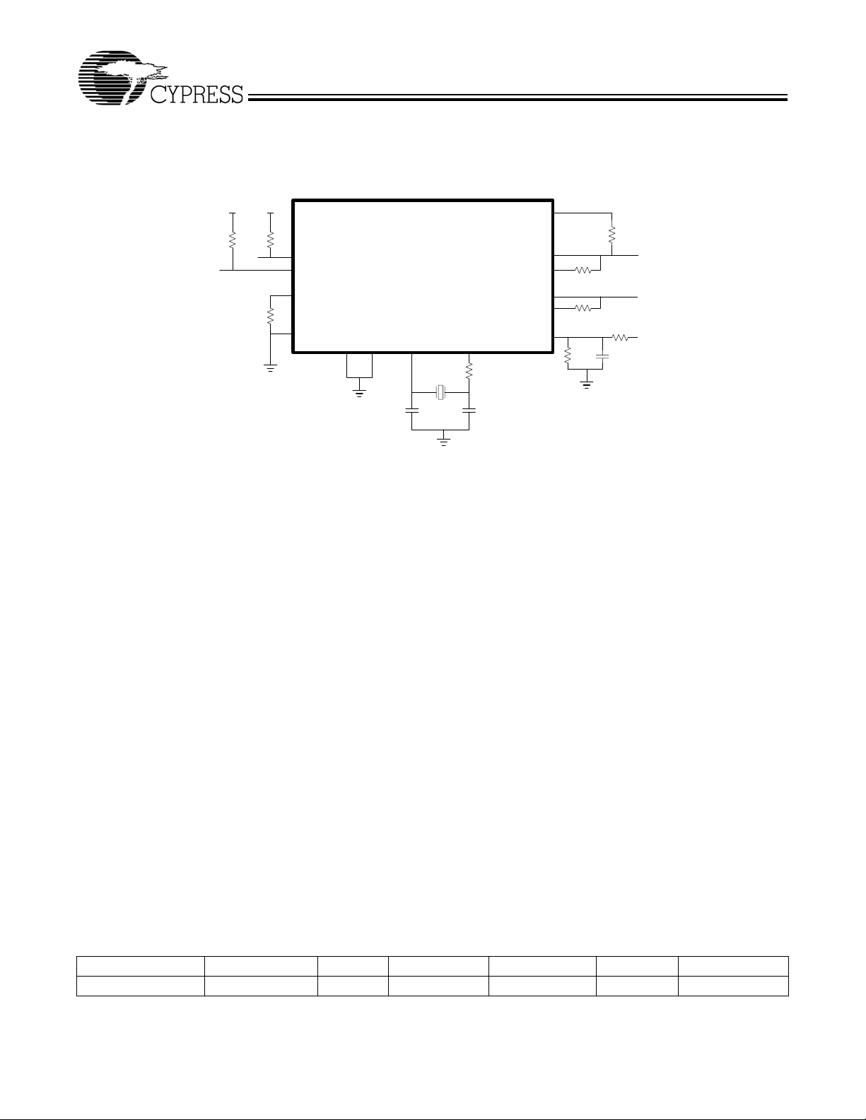
CY7C68310
6.0 External Circuitry Requirements
Certain external components are required for proper CY7C68310 operation. The following figure details the minimum required
circuitry for normal operation. Additional components may be required to support configurable CY7C68310 features, if utilized.
3.3V
3.3V
1.5KΩ
1.5KΩ
SDA
2.4KΩ
(1%)
SCL
RREF
AVSS
TMC[1:2]
SCANEN
CY7C68310
XI
30MHz
XO
100Ω
9pF9pF
Figure 6-1. External Circuitry Requirements
6.1 ATA Interface Termination
Design practices as outlined in the ATA/ATAPI-6 specification for signal integrity should be followed with systems that utilize a
ribbon cable interconnect between the CY7C68310’s ATA interface and the attached ATA/ATAPI device, especially if Ultra DMA
Mode is utilized.
RPU
DP
RSDP
DM
RSDM
VBUSPWRVLD
39Ω
39Ω
62KΩ
1.5KΩ
39KΩ
0.1µF
D+
D-
VBUS
6.2 Power Supply Regulation
At no time should the 3.3V power rail drop below the 2.5V rail for proper device operation. Care should be taken to ensure that
the power rails rise and fall without allowing the 3.3V supply to drop below the 2.5V supply. The recommended method is to
cascade voltage regulating circuits such that the 2.5V supply is powered from the 3.3V supply.
6.3 Pull-ups/Pull-downs on High-Z Pins
Certain output pins act as open-drain and remain at a high-Z state unless asserting a ‘0.’ These pins include SCL, SDA,
LOWPWR, and nPWR500. If their functionality is utilized, these pins must be tied to pull-up resistors to avoid floating while in a
high-Z state. These pins can be left as no-connects if the functionality is not utilized.
7.0 Manufacturing Interconnect Test Support
Manufacturing Test Mode is provided as a means to implement board- and system-level interconnect tests. During Manufacturing
Test Mode operation, all outputs not associated directly with USB operation are controllable. Normal state machine and register
control of output pins are disabled. Two vendor-specific USB requests (LOAD_MFG_DATA and READ_MFG_DATA) are used in
Manufacturing Test Mode operation.
7.1 LOAD_MFG_DATA
This USB request is used to enable and control Manufacturing Test Mode operation. While in Manufacturing Test Mode, individual
pins may be asserted or deasserted depending upon the contents of the data field. The DD and GPIO pins may also be set to a
high-Z state in preparation for READ_MFG_DATA command operations. Control of the select CY7C68310 I/O pins and their highZ controls are mapped to the USB data packet associated with this request.
Table 7-1. LOAD_MFG_DATA Command Format
Label bmRequestType bRequest wValue wIndex wLength Data
LOAD_MFG_DATA 0x40 0x05 Disable/Enable Starting Address Data Length Mfg. Test Data
Document #: 38-08030 Rev. *G Page 32 of 38
CY7C68310
Legal values for wValue are as follows:
• 0x0000 Normal operation mode – returns CY7C68310 to normal operation regardless of previous command data sets
(power-on reset default).
• 0x0001 Manufacturing Test Mode – manufacturing test registers control specific CY7C68310 outputs cells to enable board
Legal values for wLength are as follows:
• 0x0000 Valid only when wValue = 0x0000; used when disabling Manufacturing Test Mode of operation
• 0x0007 Valid only when wValue = 0x0001. For proper Manufacturing Test Mode operation, wLength must equal 0x0007.
Table 7-2. Bit-wise Mapping of LOAD_MFG_DATA Test Data
Byte Bit(s) Test/High-Z Control Register Name
00 LOWPWR
0 1 Reserved – Value will not affect output
0 2 nPWR500
03 nATARST
04 nDIOW
05 nDIOR
06 nDMACK
0 7 ATAPUEN
1 0 Reserved – Value will not affect output
1 2:1 nCS[1:0]
1 5:3 DA[2:0]
16 SCL
1 7 DD_EN – ‘1’ = Enable output (set for writes), ‘0’ = high-Z DD[15:0] (set for reads)
2 7:0 DD[7:0]
3 7:0 DD[15:8]
4 2:0 GPIO[2:0]
4 3 Reserved – Value will not affect output
4 6:4 GPIO_EN[2:0] – ‘1’ = Enable output (set for writes), ‘1’ = high-Z GPIO[2:0] (set for reads)
4 7 Reserved – Value will not affect output
5 7:0 Reserved – Value will not affect output
level testing in the manufacturing environment.
Any data packet lengths greater than 7 will result in a STALL condition.
7.2 READ_MFG_DATA
This USB request returns a “snapshot in time” of selected input pins. The input pin states are bit-wise mapped to the USB data
packed associated with this request. CY7C68310 input pins not associated directly with USB operation can be sampled at any
time during normal or Manufacturing Test Mode operation. This request is independent of normal CY7C68310 state machine
control or Manufacturing Test Mode write operations.
Table 7-3. READ_MFG_DATA Command Format
Label bmRequestType bRequest wValue wIndex wLength Data
READ_MFG_DATA 0xC0 0x06 0x00 0x00 Data Length Mfg. Test Data
Legal values for wValue are as follows:
• 0x0000 wValue must be set to 0x0000.
Legal values for wLength are as follows:
• 0x0001–0x0008 Any wLength value greater than 0x0008 will result in a STALL response.
Document #: 38-08030 Rev. *G Page 33 of 38

Table 7-4. Bit-wise Mapping of READ_MFG_Data Test Data
Byte Bit(s) Pin Name
00DRVPWRVLD
0 1 VBUSPWRVLD
0 2 VBUSPWRD
0 3 DISKRDY
0 4 SYSIRQ
0 5 IORDY
06DMARQ
07nEJECT
10ATAIRQ
1 1 Will always return ‘1’
12LOWPWR
1 3 Reserved – Disregard value
1 4 nPWR500
15nATARST
16nDIOW
17nDIOR
20nDMACK
2 1 ATAPUEN
2 2 Reserved – Disregard value
2 4:3 nCS[1:0]
2 7:5 DA[2:0]
3 7:0 DD[7:0]
4 7:0 DD[15:8]
5 2:0 GPIO[2:0]
5 3 Will always return ‘0’
54DD_EN
5 7:5 GPIO_EN[2:0]
6 0 MFG_SEL (manufacturing test mode enable)
6 1 ATAEN
6 2:7 Will always return ‘1’
7 7:0 Will always return ‘1’
CY7C68310
8.0 Absolute Maximum Ratings
Storage Temperature ................................................................................................................................................ –65 to 150°C
Ambient Temperature with power supplied ..................................................................................................................... 0 to 70°C
Supply Voltage to Ground Potential ...........................................................................................................................–0.5 to 5.5 V
DC Input Voltage to Any Input Pin .............................................................................................................................–0.5 to 5.5 V
DC Voltage Applied to Outputs in high-Z ...................................................................................................................–0.5 to 5.5 V
Power Dissipation .............................................................................................................................................................235 mW
Static Discharge Voltage (Meets NEC ASIC ESD specifications IEC-GQ-6002-01 and IEC-6005-01) ........................... > 2000 V
Max Output Current per I/O port..........................................................................................................................................20 mA
Latch-up Current.............................................................................................................................................................> 200 mA
Document #: 38-08030 Rev. *G Page 34 of 38

CY7C68310
9.0 Operating Conditions
Operating temperature.................................................................................................................................................... 0 to 70°C
10.0 DC Characteristics
Parameter Description Min. Typ. Max. Unit
V
DD
V
DDA
V
DDIO
V
IH
V
IL
V
OH
V
OL
I
OH
I
OL
I
nCFG
I
CC
I
SUP
I
SLP
Note: All values in this table assume 25°C ambient temperature and nominal voltage unless otherwise stated. All “Configured operational” measurements assume a 50/50 read/write duty cycle.
Digital voltage supply 2.25 2.50 2.75 V
Analog voltage supply 2.25 2.50 2.75 V
I/O cell voltage supply 3.0 3.3 3.6 V
Input high voltage 2.0 V
+ 0.5 V
DDIO
Input low voltage –0.5 0.8 V
Output high voltage at I
Output low voltage at I
Source current at V
Sink current at V
Unconfigured
current
Configured
OH
OL
Full-speed 40 mA
High-speed 60 mA
Full-speed 2.5V Supply 36 mA
idle
OH
OL
3.3V Supply 2 mA
2.4 V
0.4 V
6mA
6mA
High-speed 2.5V Supply 55 mA
3.3V supply 2 mA
Configured
operational
Current in USB suspend
Full-speed 2.5V Supply 53 mA
3.3V Supply 11 mA
High-speed Compact
Flash
2.5” HDD
(See Note)
3.5” HDD
(See Note)
2.5V Supply 65 mA
3.3V Supply 6 mA
2.5V Supply 73 mA
3.3V Supply 9 mA
2.5V Supply 74 mA
3.3V Supply 19 mA
250 µA
(inactive, connected)
Current in Sleep mode
0.7 10 µA
(inactive, unconnected)
11.0 Ordering Information
Part Number [Package Type
CY7C68310-80AC 80-Lead TQFP
CY7C68310-80AZC
CY4617 CY7C68310 Mass Storage Reference Design Kit
Note:
1. The Lead-Free option should be used for new designs. It is recommended that existing designs migrate to Lead-Free parts.
Document #: 38-08030 Rev. *G Page 35 of 38
[1]
80-Lead TQFP Lead-Free Package

12.0 Package Diagram
80-lead Thin Plastic Quad Flat Pack (12 x 12 x 1.0 mm) A8012x12
CY7C68310
51-85175-**
Figure 12-1. 80-pin TQFP Package Diagram
13.0 PCB Layout Recommendations
The CY7C68310 contains high-speed analog circuitry that is sensitive to system noise. In particular, noise on both analog and
digital power supplies must be minimized to ensure reliable, high-performance operation. Special attention should also be given
to the design of the frequency generation, voltage reference, and USB interface circuits. Cypress recommends using the following
guidelines in designing any product that uses the CY7C68310.
• The 3.3V power rail must remain above the 2.5V rail at all times for proper device operation.
• DP and DM trace lengths should be kept to within 2 mm of each other and must not exceed 37 mm in total length, with a
preferred length of 20–30 mm.
• Maintain a solid ground plane under the DP and DM traces. Do not allow the plane to be split under these traces.
• Do not place vias on the DP or DM traces.
• Isolate the DP and DM traces from all other signal traces by no less than 10 mm.
• The DP and DM common mode trace impedance should be controlled to 45
90
Ω (±10%).
• The VDD power plane should be as solid as possible with direct paths from the voltage regulator to all discrete components.
A four layer board is required with inner layers dedicated to power and ground planes. Digital ground should cover one entire
layer of the design.
• Analog and digital power planes must be isolated using inductors.
• Ceramic or tantalum capacitors are required. Do not use electrolytic capacitors. Electrolytic capacitors have higher lead
inductance and series resistance values that have been observed to contribute to increased power supply noise.
• Adequate bypass capacitance must be implemented very near to the CY7C68310 power pins. One ceramic bypass capacitor
per power/ground pair is recommended.
Ω with total differential impedance controlled to
Document #: 38-08030 Rev. *G Page 36 of 38

CY7C68310
• All termination and pull-up resistors (including DP and DM) should be placed within 5 mm of the CY7C68310 pins.
• The crystal and RREF external resistor components should be placed as near the CY7C68310 pins as possible.
14.0 Disclaimers, Trademarks, and Copyrights
Purchase of I2C components from Cypress, or one of its sublicensed Associated Companies, conveys a license under the Philips
2
C Patent Rights to use these components in an I2C system, provided that the system conforms to the I2C Standard Specification
I
as defined by Philips. ISD-300LP is a trademark of Cypress Semiconductor. All product and company names mentioned in this
document are the trademarks of their respective holders.
Document #: 38-08030 Rev. *G Page 37 of 38
© Cypress Semiconductor Corporation, 2004. The information contained herein is subject to change without notice. Cypress Semiconductor Corporation assumes no responsibility for the use
of any circuitry other than circuitry embodied in a Cypress Semiconductor product. Nor does it convey or imply any license under patent or other righ ts. Cypress Semiconductor does not authorize
its products for use as critical components in life-support systems where a malfunction or failure may reasonably be expected to result in significant injury to the user. The inclusion of Cypress
Semiconductor products in life-support systems application implies that the manufacturer assumes all risk of such use and in doing so indemnifies Cypress Semiconductor against all charges.

Document History Page
Description Title: CY7C68310 ISD-300LP™ Low-Power USB 2.0 to ATA/ATAPI Bridge IC
Document Number: 38-08030
REV. ECN No. Issue Date
** 118297 09/18/02 BHA New Data Sheet
*A 120307 12/12/02 GIR Revised for Preliminary status
*B 123509 04/04/03 GIR Revised to include first silicon information
*C 126049 04/07/03 CVR Post to external website CY7C68310-80AC
*D 126323 05/21/03 GIR Updated Suspend Current and included Sleep Mode in Section 10.0
*E 127185 06/05/03 BEH Changed Static Discharge voltage to > 2000V(1)
*F 127739 09/03/03 GIR Corrected formatting of all tables
*G 131946 02/06/04 KKU Updated to include lead-free part numbers.
Orig. of
Change Description of Change
Added ESD Testing Methodology and Power Dissipation values to Section 8.0
Revised for Final status
Replaced previous Status Discharge footnotes with the following: “1. Meets NEC
ASIC ESD specifications IEC-GQ-6002-01 and IEC-6005-01”
Changed DC Specification I
Added sections on ATACB and ATACB2
Corrected pin descriptions in Sections 2.3.4, 2.3.6, 2.3.8, 2.3.15, 2.3.16, and 2.3.17
Corrected values/contents of some EEPROM table fields to clarify IROS contents
Divided 2.5V and 3.3V current consumption in Section 10
Swapped order of PCB Layout Guidelines and Package Diagram sections
Corrected spelling and grammar
Added USB certification logo to cover page
Added USB-IF test ID number to Section 1.1 list
Section 1.1 changed “Compact 80-Lead TQFP” to “Compact 80-pin TQFP package
with a Lead-Free option”
Section 11.0 added: CY7C68310-80AZC 80-Lead TQFP Lead-Free Package with
footnote that new designs should use Lead-Free part and existing designs should
migrate to Lead-Free parts.
<10 uA typical to 10 uA max
SLP
CY7C68310
Document #: 38-08030 Rev. *G Page 38 of 38
 Loading...