

Page 1

FS781/82/84
Low EMI Spectrum Spread Clock
Features
• Spread Spectrum clock generator (SSCG) with 1×, 2×,
and 4× outputs
• 6- to 82-MHz operating frequency range
• Modulates external clocks including crystals, crystal
oscillators, or ceramic resonators
• Programmable modulation with simple R-C external
loop filter (LF)
• Center spread modulation
• 3V-5V power supply
• TTL-/CMOS-compatible outputs
• Low short-term jitter
• Low-power Dissipation
— 3.3 VDC = 37 mW – typical
— 5.0 VDC = 115 mW – typical
• Available in 8-pin SOIC and TSSOP packages
Applications
• Desktop/notebook computers
• Printers, copiers, and MFP
• Scanners and fax
• LCD displays and monitors
• CD-ROM, VCD, and DVD
• Automotive and embedded systems
• Networking, LAN/WAN
• Digital cameras and camcorders
•Modems
Benefits
Functional Description
The Cypress FS781/82/84 are Spread Spectrum clock
generator ICs (SSCG) designed for the purpose of reducing
electromagnetic interference (EMI) found in today’s
high-speed digital systems.
The FS781/82/84 SSCG clocks use a Cypress-proprietary
technology to modulate the input clock frequency, XIN, by
modulating the frequency of the digital clock. By modulating
the reference clock the measured EMI at the fundamental and
harmonic frequencies of FSOUT is greatly reduced. This
reduction in radiated energy can significantly reduce the cost
of complying with regulatory requirements without degrading
digital waveforms.
The Cypress FS781/82/84 clocks are very simple and
versatile devices to use. By programming the two range select
lines, S0 and S1, any frequency from 6- to 82-MHz operating
range can be selected. The FS781/2/4 are designed to
operate over a very wide range of input frequencies and
provides 1×, 2×, and 4× modulated clock outputs.
The FS78x devices have a simple frequency selection table
that allows operation from 6 MHz to 82 MHz in four separate
ranges. The bandwidth of the frequency spread at FSOUT is
determined by the values of the loop filter components. The
modulation rate is determined internally by the input frequency
and the selected input frequency range.
The Bandwidth of these products can be programmed from as
little as 1.0% up to as much as 4.0% by selecting the proper
loop filter value. Refer to the Loop Filter Selection chart in
Table 2 and Table 3 for the recommended values. Due to a
wide range of application requirements, an external loop filter
(LF) is used on the FS78x products. The user can select the
exact amount of frequency modulation suitable for the application. Using a fixed internal loop filter would severely l imit
the use of a wide range of modulation bandwidths (Spread %)
to a few discrete values. Refer to FS791/2/4 products for applications requiring 80- to 140-MHz frequency range.
• Programmable EMI reduction
• Fast time to market
• Lower cost of compliance
• No degradation in rise/fall times
• Lower component and PCB layer count
Cypress Semiconductor Corporation • 198 Champion Court • San Jose, CA 95134-1709 • 408-943-2600
Document #: 38-07029 Rev. *F Revised January 2, 2005
[+] Feedback
Page 2
FS781/82/84
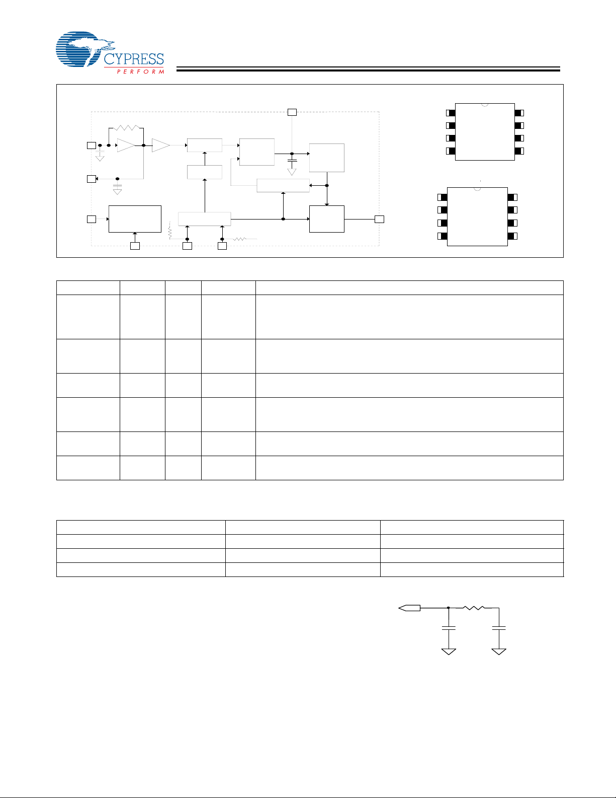
Block Diagram
250 K
1(3)
Xin
Xout
VDD
8 pF
2(4)
Power Contol
8(2)
Logic
VSS
Loop Filter
4(6)
Reference
Divider
Modulation
Control
8 pF
Input Control Logic
VDD
5(7)
3(5)
Phase
Detector
10 pF.
VCO / N
7(1)
S0S1
VSS
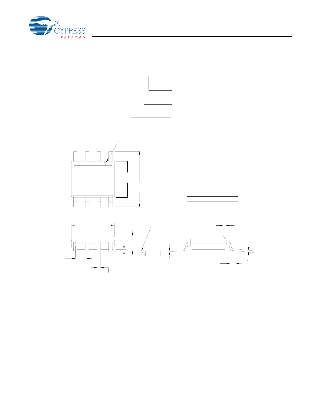
Pin Configuration
VCO
Output
Divider
and
Mux
(TSSOP Pin #)
6(8)
Pin Description
Pin Name I/O Type Description
1/2 (SOIC)
3/4 (TSSOP)
7/3 (SOIC)
1/5 (TSSOP)
4 (SOIC)
6 (TSSOP)
6 (SOIC)
8 (TSSOP)
8 (SOIC)
2 (TSSOP)
5 (SOIC)
7 (TSSOP)
X
IN/XOUT
I/O Analog Pins form an on-chip reference oscillator when connected to terminals
of an external parallel resonant crystal. X
TTL/CMOS external clock source. If X
other than crystal, leave X
OUT
S0 / S1 I CMOS/TTL Digital control inputs to select input frequency range and output
frequency scaling. Refer to Table 2 and Table 3 for selection. S0 has internal
pull-down. S1 has internal pull-up.
LF I Analog Loop Filter. Single ended three-state output of the phase detector. A two-pole
passive loop filter is connected to LF.
FSOUT O CMOS/TTL Modulated Clock Frequency Outp ut. The center frequency is the same as
the input reference frequency for FS781. Input frequency is multiplied by 2×
and 4× for FS782 and FS784, respectively.
V
DD
V
SS
P Power Positive Power Supply.
P Power Power Supply Ground.
Xin
Xout
S1
LF
8 Pin SOIC Package
1
S0
VDD
FSOUT
Xout
is connected to an external clock
IN
(pin 2) unconnected.
2
3
Xin
4
8 Pin TSSOP Packag e
may be connected to
IN
1
2
3
4
FS78x
FS78x
VDD
8
S0
7
FSOUT
6
VSS
5
8
FSOUT
7
VSS
6
LF
5
S1
Output Frequency Selection
Table 1. FSOUT SSCG (Modulated Output Clock) Product Selection
Product Number FSOUT Frequency Scaling Description
FS781 1× 1× modulated frequency of input clock
FS782 2× 2× modulated frequency of input clock
FS784 4× 4× modulated frequency of input clock
Loop Filter Selection Chart
The following table provides a list of recommended loop filter
values for the FS781/82/84. The FS78X is divided into four
ranges and operated at both 3.3V and 5.5 VDC. The loop filter
at the right is representative of the loop filter components in
Table 2.
Document #: 38-07029 Rev. *F Page 2 of 12
LF (pin 4)
R6
C8
C7
[+] Feedback
Page 3
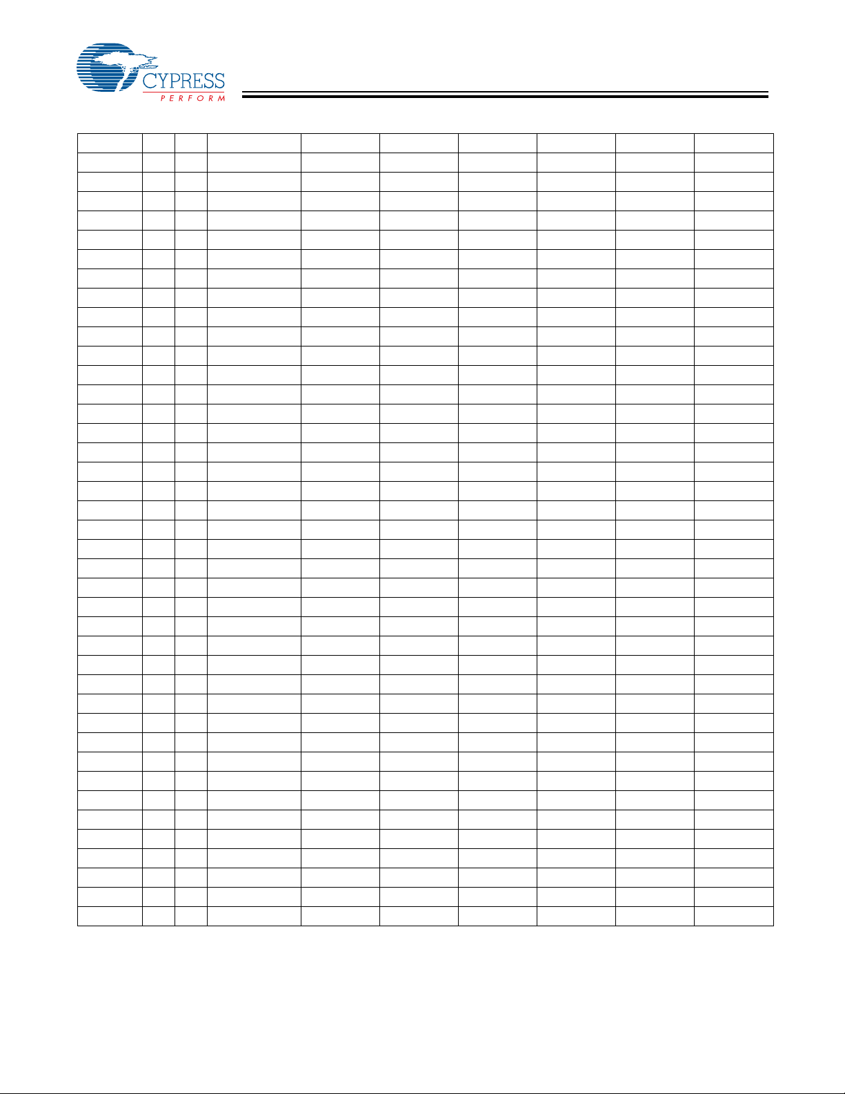
FS781/82/84
Table 2. FS781/82/84 Recommended Loop Filter Values C7 (pF) @ +3.3 VDC ±5% (R6 = 3.3K)
Input MHz S1 S0 BW = 1.0%
[3]
BW = 1.5%
[3]
BW = 2.0%
[3]
BW = 2.5%
[3]
BW = 3.0%
[1, 2, 3, 4]
[3]
BW = 3.5%
[3]
6 0 0 10,000/1000 1550 910 780 700 640 560
8 0 0 10,000/330 990 820 640 520 450 400
10 0 0 1040 680 460 360 300 240 210
12 0 0 830 420 300 220 200 190 170
14 0 0 580 230 200 160 140 100 80
16 0 1 10000 980 760 580 470 410 385
18 0 1 1200 750 580 470 415 370 300
20 0 1 1000 730 470 390 320 220 190
22 0 1 960 640 410 270 230 200 180
24 0 1 920 400 250 210 180 160 150
26 0 1 660 300 220 180 150 140 120
28 0 1 470 230 180 150 130 100 70
30 0 1 470 180 140 120 100 80 60
32 0 1 330 170 120 100 82 68 47
34 1 0 10000 860 640 520 430 380 330
36 1 0 2200 820 620 470 400 330 290
38 1 0 1500 690 520 410 340 290 240
40 1 0 960 600 420 340 280 220 160
42 1 0 940 620 380 275 230 210 180
44 1 0 950 680 400 250 210 190 170
46 1 0 900 580 270 220 190 180 165
48 1 0 790 440 260 210 180 160 140
50 1 0 660 360 250 190 170 150 140
52 1 0 470 325 220 185 155 135 120
54 1 0 470 270 200 170 140 130 100
56 1 0 445 250 185 150 120 85 47
58 1 0 430 210 165 130 100 65 33
60 1 0 295 185 150 120 100 90 82
62 1 0 270 220 150 120 100 82 68
64 1 1 1180 860 560 410 340 290 230
65 1 1 1180 850 540 400 330 280 220
66 1 1 1180 760 560 350 260 220 210
68 1 1 1180 750 500 320 260 230 210
70 1 1 1120 740 470 370 300 240 170
72 1 1 1160 780 470 300 250 220 190
74 1 1 1110 770 470 280 230 210 190
76 1 1 1000 720 440 240 210 190 170
78 1 1 910 670 270 210 190 170 160
80 1 1 900 620 260 210 190 170 156
82 1 1 900 540 250 210 190 170 150
Notes:
1. If the value selected from the above chart is not a standard, use the next available larger value.
2. All bandwidths indicated above are total peak-to-peak spread. 1% = +0.5% to –0.5%. 4% = +2.0% to –2.0%.
3. If C8 is not listed in the chart for a particular bandwidth and frequency, it is not used in t he loop filter.
4. Contact Cypress for LF values less than 1.0% bandwidth.
BW = 4.0%
[3]
Document #: 38-07029 Rev. *F Page 3 of 12
[+] Feedback
Page 4
FS781/82/84
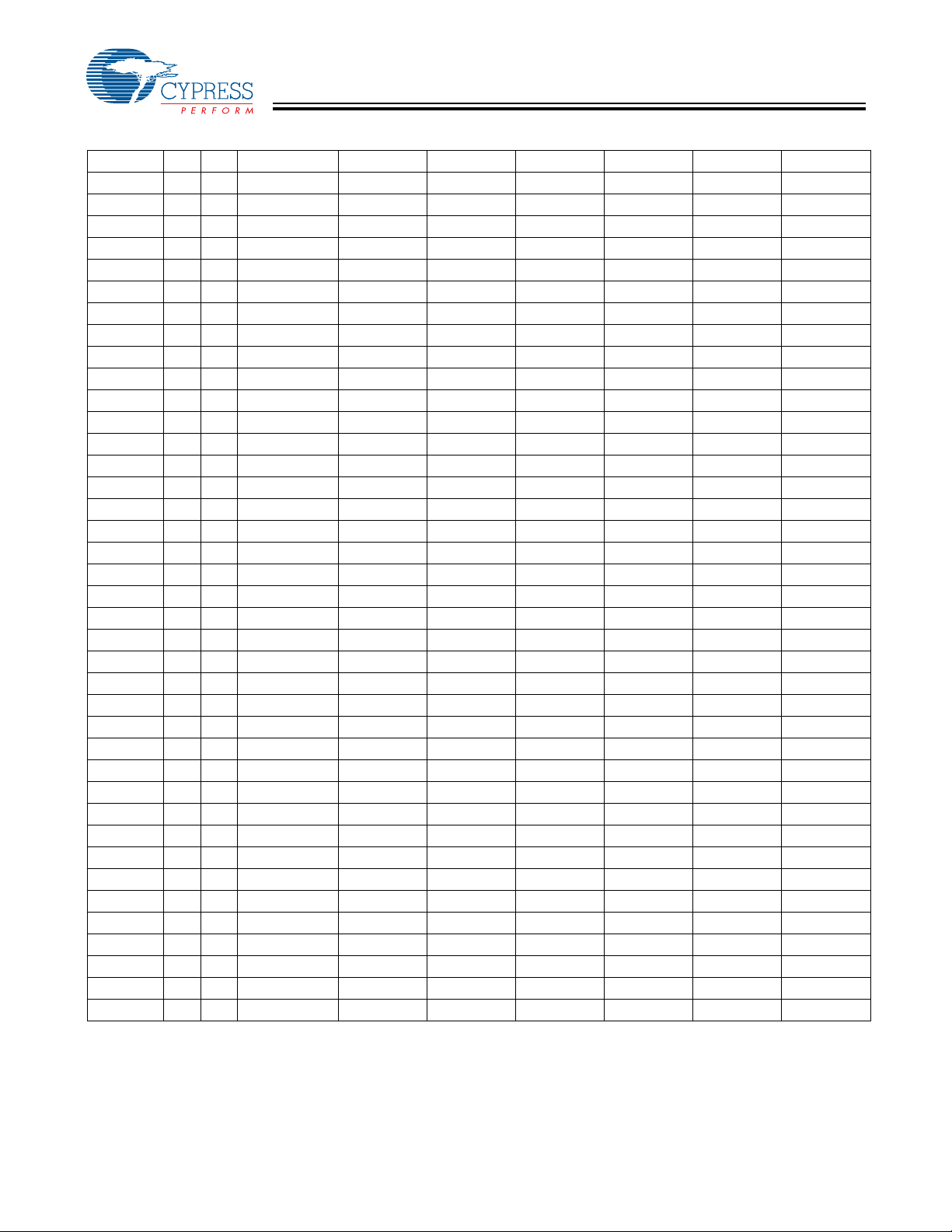
Table 3. FS781/82/84 Recommended Loop Filter Values C7 (pF) @ +5.0 VDC ±5% (R6 = 3.3K)
Input MHz S1 S0 BW = 1.0%
[3]
BW = 1.5%
[3]
BW = 2.0%
[3]
BW = 2.5%
[3]
BW = 3.0%
[1, 2, 3, 4]
[3]
BW = 3.5%
6 0 0 1140 1030 930 830 710 610 510
8 0 0 1170 970 740 570 460 400 280
10 0 0 1030 660 430 350 280 210 130
12 0 0 760 340 230 200 180 160 130
14 0 0 450 240 180 140 100 70 50
16 0 1 2490 970 730 590 480 430 370
18 0 1 2490 870 650 510 430 370 310
20 0 1 1360 680 480 370 280 190 250
22 0 1 990 560 330 260 230 200 190
24 0 1 820 360 250 200 180 160 150
26 0 1 530 270 210 170 150 110 90
28 0 1 430 230 180 150 110 100 90
30 0 1 250 200 150 110 100 90 80
32 1 0 Note 4 1000 740 570 470 410 370
34 1 0 Note 4 990 710 520 420 360 300
36 1 0 Note 4 970 670 480 380 310 230
38 1 0 Note 4 880 560 380 310 270 220
40 1 0 Note 4 800 460 290 240 230 220
42 1 0 1030 680 360 260 220 200 190
44 1 0 790 560 260 220 200 190 170
46 1 0 1110 420 280 210 180 170 140
48 1 0 1110 280 200 190 170 140 120
50 1 0 830 330 200 180 160 130 110
52 1 0 560 340 205 170 140 120 90
54 1 0 510 280 180 140 110 110 90
56 1 0 470 210 160 120 100 90 90
58 1 0 450 220 250 110 90 80 80
60 1 0 430 240 120 90 80 80 70
62 1 1 Note 4 800 580 430 330 250 180
64 1 1 Note 4 720 490 375 285 200 140
66 1 1 Note 4 630 400 320 240 150 100
68 1 1 Note 4 690 365 285 225 170 140
70 1 1 Note 4 650 330 250 210 190 180
72 1 1 Note 4 575 340 250 210 190 170
74 1 1 Note 4 500 355 245 205 180 165
76 1 1 Note 4 550 330 230 200 175 160
78 1 1 Note 4 600 290 220 190 170 155
80 1 1 Note 4 570 240 210 185 165 150
82 1 1 Note 4 540 250 200 180 160 140
[3]
BW = 4.0%
[3]
Document #: 38-07029 Rev. *F Page 4 of 12
[+] Feedback
Page 5

Table 4. Modulation Rate Divider Ratios
S1 S0 Input Frequency Range (MHz) Modulation Divider Number
0 0 6 to 16 120
0 1 16 to 32 240
1 0 32 to 66 480
1 1 66 to 82 720
FS781/82/84
SSCG Modulation Profile
The digital control inputs S0 and S1 determine the modulation
frequency of FS781/2/4 products. The input frequency is
divided by a fixed number, depending on the operating range
that is selected. The modulation frequency of the FS78x can
be determined from Table 4. To compute the modulation
frequency, determine the values of S0 and S1, and find the
modulation divider number in Table 4.
Theory of Operation
The FS781/82/84 devices are phase-locked loop-(PLL)-type
clock generators using Direct Digital Synthesis (DDS). ‘By
precisely controlling the bandwidth of the output clock, the
FS781/2/4 products become a low-EMI clock generator. The
theory and detailed operation of these products will be
discussed in the following sections.
EMI
All clocks generate unwanted energy in their harmonics.
Conventional digital clocks are square waves with a duty cycle
that is very close to 50%. Because of the 50/50 duty cycle,
digital clocks generate most of their harmonic energy in the
odd harmonics (e.g., third, fifth, seventh). It is possible to
reduce the amount of energy contained in the fundamental
and harmonics by increasing the bandwidth of the fundamental clock frequency. Conventional digital clocks have a
very high Q factor, which means that all of the energy at that
frequency is concentrated in a very narrow bandwidth, conse-
quently, higher energy peaks. Regulatory agencies test
electronic equipment by the amount of peak energy radiated
from the equipment. By reducing the peak energy at the fundamental and harmonic frequencies, the equipment under test is
able to satisfy agency requirements for EMI. Conventional
methods of reducing EMI have been to use shielding, filtering,
multi-layer PCBs, etc. These FS781/2 and 4 reduce the peak
energy in the clock by increasing the clock bandwidth and
lowering the Q of the clock.
SSCG
The FS781/82/84 products use a unique method of modulating
the clock over a very narrow bandwidth and controlled rate of
change, both peak to peak and cycle to cycle. The FS78x
products take a narrow band digital reference clock in the
range of 6–82 MHz and produce a clock that sweeps between
a controlled start and stop frequency and precise rate of
change. To understand what happens to an SSCG clock,
consider that we have a 20-MHz clock with a 50% duty cycle.
From a 20-MHz clock we know the following:
Clock Frequency = Fc = 20 MHz.
Clock Period = Tc = 1/20 MHz = 50 ns.
Consider that this 20-MHz clock is applied to the X
the FS78x as either an externally driven clock or the result of
a parallel resonant crystal connected to pins 1 and 2 of the
FS78x. Also consider that the products are operating from a
5V DC power supply and the loop filter is set for a total
bandwidth spread of 2%. Refer to Figure 2.
input of
IN
+ .5%
1.0%
Xin
Total
- .5%
TIME (microseconds)
Note:
5. With the correct loop filter connected to Pin 4, the following profile will provide the best EMI reduction. This profile can be seen on a Time Domain Analyzer.
Document #: 38-07029 Rev. *F Page 5 of 12
Figure 1. Frequency Profile in Time Domain
[5]
[+] Feedback
Page 6
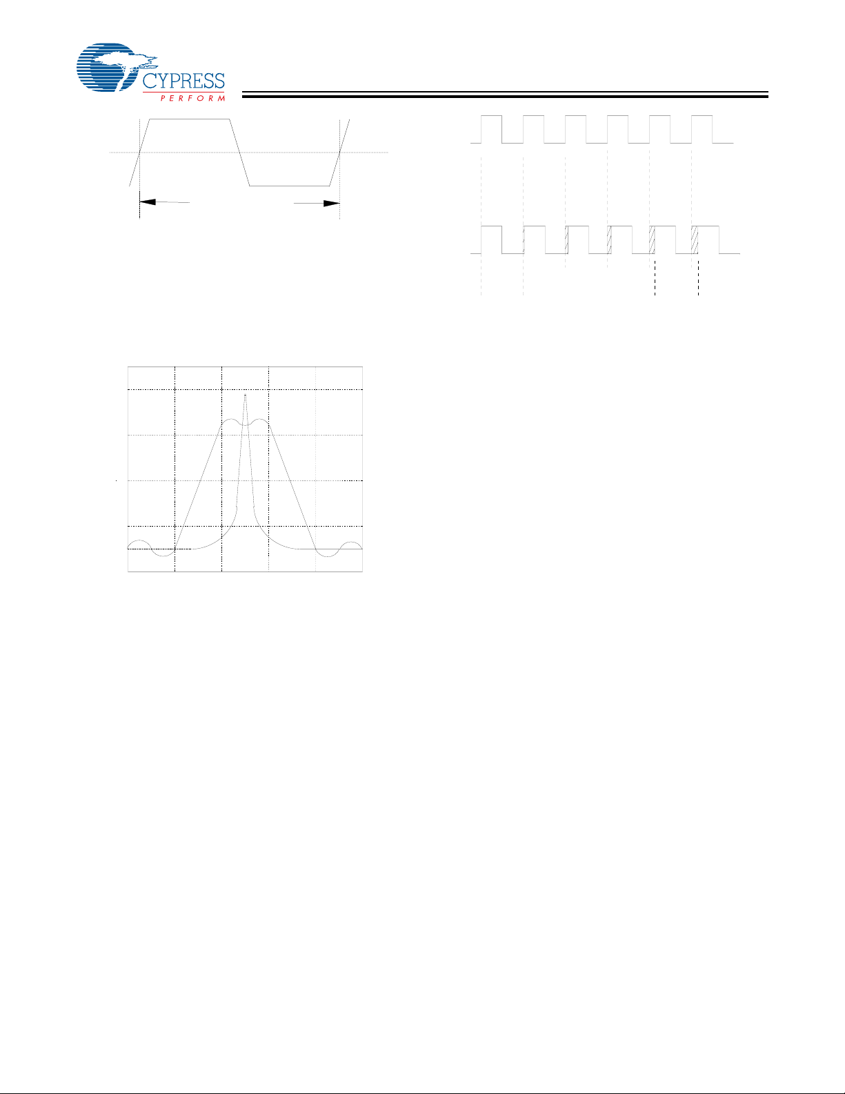
50% 50%
n
Tc = 50 ns.
Figure 2. 20-MHz Unmodulated Clock
From the above parameters, the output clock at FSOUT will be
sweeping symmetrically around a center frequency of 20 MHz.
The minimum and maximum extremes of this clock will be
+200 kHz and –200 kHz. So we have a clock that is sweeping
from 19.8 MHz to 20.2 MHz and back again. If we were to look
at this clock on a spectrum analyzer we would see the picture
in Figure 3. Keep in mind that this is a drawing of a perfect
clock with no noise.
Fc = 20 MHz
Fmin =
19.8 MHz
Figure 3. Spectrum Analysis of 19.8–20.2 MHz Clock
We see that the original 20-MHz reference clock is at the
center frequency (Cf), and the min. and max. extremes are
positioned symmetrically about the center frequency. This type
of modulation is called Center-Spread. Figure 4 shows a
20-MHz clock as it would be seen on an oscilloscope. The top
trace is the non-modulated reference clock. The bottom trace
is the modulated clock at pin 6. From this comparison chart
you can see that the frequency is decreasing and the period
of each successive clock is increasing. The Tc mea surement s
on the left and right of the bottom trace indicate the max. and
min. extremes of the clock. Intermediate clock changes are
small and accumulate to achieve the total period deviation.
The reverse of this figure would show the clock going fro m
minimum extreme back to the high extreme.
Fmax =
20.2 MHz
FS781/82/84
Tc =49.50 ns.
Figure 4. Period Comparison Chart
Looking at Figure 3, you will note that the peak amplitude of
the 20-MHz non-modulated clock is higher than the wideband
modulated clock. This difference in peak amplitudes between
modulated and unmodulated clocks is the reason why SSCG
clocks are so effective in digital systems. This figure refers to
the fundamental frequency of a clock. A very important characteristic of the SSCG clock is that the bandwidth of the fundamental frequency is multiplied by the harmonic number. In
other words, if the bandwidth of a 20-MHz clock is 200 kHz,
the bandwidth of the third harmonic will be 3 × 200, or 600 kHz.
The amount of bandwidth is relative to the amount of energy
in the clock. Consequently, the wider the bandwidth, the
greater the energy reduction of the clock.
Most applications will not have a problem meeting agency
specifications at the fundamental frequency. It is the higher
harmonics that usually cause the most problems. With an
SSCG clock, the bandwidth and peak energy reduction
increases with the harmonic number. Consider that the
eleventh harmonic of a 20-MHz clock is 220 MHz. With a total
spread of 200 kHz at 20 MHz, the spread at the eleventh
harmonic would be 2.20 MHz, which greatly reduces the peak
energy content. It is typical to see as much as 12- to 18-dB
reduction at the higher harmonics, due to a modulated clock.
The difference in the peak energy of the modulated clock and
the non-modulated clock in typical applications will see a
2–3dB reduction at the fundamental and as much as 8 – 10
dB reduction at the intermediate harmonics: third, fifth,
seventh, etc. At the higher harmonics, it is quite possible to
reduce the peak harmonic energy, compared to the unmodulated clock, by as much as 12 to 18 dB.
Application Notes and Schematic
Figure 5 is configured for the following parameters:
Package selected = FS781.
X
= 20-MHz crystal
IN
FSOUT = 20 MHz (S0 = 1 and S1 = 0).
Bandwidth of the FSOUT clock is determined by the values of
the loop filter connected to pin 4.
Tc = 50.50
Document #: 38-07029 Rev. *F Page 6 of 12
[+] Feedback
Page 7

FS781/82/84
Crystal is 20 MHz is 1st Order
with 18 pF load capacitance.
If Crystal load capacitance is
different than 18 pF, C1 and C2
must be re-calculated.
For third overtone crystals, a
parallel or series resonant tr ap
is required.
Mount loop filter components as
close to LF pin as possible.
C2
27 pF
C3
27 pF
20 MHz
Y1
R6
** Occasionally, C8 is used to
create a second pole for this loop
filter. Refer to Loop Filter Selection
table.
Figure 5. FS781 Schematic
1
Xin
2
Xout
VDD
8
7
S0
C1
0.1 uF
VDD
FS781
(SOIC)
3
S1
4
LF
C8C7
FSOUT
VSS
6
5
FSOUT
**
.
Document #: 38-07029 Rev. *F Page 7 of 12
[+] Feedback
Page 8

FS781/82/84
Absolute Maximum Ratings
This device contains circuitry to protect the input against
damage due to high static voltages or electric fields; however,
precautions should be taken to avoid application of any
voltage higher than the absolute maximum rated voltages to
[6]
this circuit. For proper operation, VIN and V
constrained to the range, V
inputs are tied high or low internally. Refers to electrical speci-
< (VIN or V
SS
OUT
should be
OUT
) < VDD. All digital
fications for operating supply range.
Table 5. Absolute Maximum Ratings
Parameter Description Min. Max. Unit
V
DD
VIRvss Input, relative to V
VORvss Output, relative to V
Operating Voltage 3.0 6.0 VDC
SS
SS
–0.3 VDD + 0.3 VDC
–0.3 VDD + 0.3 VDC
TOP Temperature, Operating 0 +70 °C
TST Temperature, Storage –65 +150 °C
T
J
Table 6. DC Electrical Characteristics V
Temperature, Junction – +125 °C
= 3.3V and 5.0V ±10%, XIN = 48 MHz, TA = 0°C to 70°C
DD
Parameter Description Min. Typ. Max. Unit
V
IL
V
IH
I
IL
I
IH
V
OL
V
OH
V
OL
V
OH
Input Low Voltage – 0.3 * V
Input High Voltage 0.7 * V
DD
DD
VDC
VDC
Input Low Current 100 µA
Input High Current 100 µA
Output Low Voltage IOL= 10 mA, VDD = 5V 0.4 VDC
Output High Voltage IOH = 10 mA, VDD = 5V VDD – 1.0 VDC
Output Low Voltage IOL= 6 mA, VDD = 3.3V 0.4 VDC
Output High Voltage IOH = 5 mA, VDD = 3.3V 2.4 VDC
Rpd Resistor, Pull-down (Pin 7) 60K 125K 200K Ω
Rpu Resistor, Pull-up (Pin 3) 60K 125K 200K Ω
C
C
I
I
xin
xout
CC
CC
Input Capacitance (Pin 1) 8 pF
Output Capacitance (Pin 2) 10 pF
5V Dynamic Supply Current (CL = No Load) 38 mA
3.3V Dynamic Supply Current (CL = No Load) 20 mA
ISC Short Circuit Current (FSOUT) 25 mA
BW BW% Variations, 3.30V
BW BW% Variations, 5.00V
[7]
[7]
–20 0 +20 %
–30 0 +30 %
Table 7. Timing Electrical Characteristics VDD = 3.3V and 5.0V ±10%, TA = 0°C to 70°C, CL = 15 pF, XIN = 48 MHz
Parameter Description Min. Typ. Max. Unit
tTLH Output Rise Time Measured at 10%–90% @ 5 VDC 1.8 2.2 2.7 ns
tTHL Output Fall Time Measured at 10%–90% @ 5 VDC 1.5 2.0 2.5 ns
tTLH Output Rise Time Measured at 0.8V–2.0V @ 5 VDC 0.5 0.65 0.8 ns
tTHL Output Fall Time Measured at 0.8V–2.0 V @ 5 VDC 0.5 0.65 0.8 ns
tTLH Output Rise Time Measured at 10%–90% @ 3. 3 VD C 2.1 2.65 3.2 ns
tTHL Output Fall Time Measured at 10%–90% @ 3.3 VDC 1.7 2.1 2.6 ns
tTLH Output Rise Time Measured at 0.8V–2.0V @ 3.3 VDC 0.7 0.95 1.2 ns
tTHL Output Fall Time Measured at 0.8V–2.0 V @ 3.3 VDC 0.6 0.85 1.1 ns
TsymF1 Output Duty Cycle 45 50 55 %
Notes:
6. Single Pow e r Supply: The Voltage on any input or /O pin cannot exceed the power pin during power-up.
7. Percentage variations from the bandwidth % values given in
Table 2 and Table 3.
Document #: 38-07029 Rev. *F Page 8 of 12
[+] Feedback
Page 9

FS781/82/84
Table 7. Timing Electrical Characteristics V
= 3.3V and 5.0V ±10%, TA = 0°C to 70°C, CL = 15 pF , XIN = 48 MHz (continued)
DD
Parameter Description Min. Typ. Max. Unit
CCJ FSOUT, Cycle-to-Cycle Jitter, 48 MHz @ 3.30 VDC (Pin 6) – 320 370 ps
CCJ FSOUT, Cycle-to-Cycle Jitter, 48 MHz @ 5.0 VDC (Pin 6) – 310 360 ps
CCJ FSOUT, Cycle-to-Cycle Jitter, 72 MHz @ 3.30 VDC (Pin 6) – 270 325 ps
CCJ FSOUT, Cycle-to-Cycle Jitter, 72 MHz @ 5.0 VDC (Pin 6) – 390 440 ps
Table 8. Range Selection Table
S1
(pin 3)
S0
(pin 7)
Fin (MHz)
(pin 2/3)
Modulation
Rate
FS781
FSOUT (pin 6)
FS782
FSOUT (pin 6)
FS784
FSOUT (pin 6)
0 0 6–16 Fin/120 6–16 MHz 12–32 MHz 32–64 MHz
0 1 16–32 Fin/240 16–32 MHz 32–64 MHz 64–82 MHz
1 0 32–66 Fin/480 32–66 MHz 64–82 MHz N/A
1 1 66–82 Fin/720 66–82 MHz N/A N/A
Ordering Information
[8]
Part Number Package Type Product Flow
IMIFS781BZB 8-pin 150-mil SOIC Commercial, 0 to 70°C
IMIFS781BZBT 8-pin 150-mil SOIC – Tape and Reel Commercial, 0 to 70°C
IMIFS782BZB 8-pin 150-mil SOIC Commercial, 0 to 70°C
IMIFS782BZBT 8-pin 150-mil SOIC – Tape and Reel Commercial, 0 to 70°C
IMIFS784BZB 8-pin 150-mil SOIC Commercial, 0 to 70°C
IMIFS784BZBT 8-pin 150-mil SOIC – Tape and Reel Commercial, 0 to 70°C
IMIFS781BT 8-pin (4.4 mm body) TSSOP Commercial, 0 to 70°C
IMIFS781BTT 8-pin (4.4 mm body) TSSOP – Tape and Reel Commercial, 0 to 70°C
IMIFS784BT 8-pin (4.4 mm body) TSSOP Commercial, 0 to 70°C
IMIFS784BTT 8-pin (4.4 mm body) TSSOP – Tape and Reel Commercial, 0 to 70°C
Lead-free
CYIFS781BSXC 8-pin 150-mil SOIC Commercial, 0 to 70°C
CYIFS781BSXCT 8-pin 150-mil SOIC – Tape and Reel Commercial, 0 to 70°C
CYIFS782BSXC 8-pin 150-mil SOIC Commercial, 0 to 70°C
CYIFS782BSXCT 8-pin 150-mil SOIC – Tape and Reel Commercial, 0 to 70°C
CYIFS784BSXC 8-pin 150-mil SOIC Commercial, 0 to 70°C
CYIFS784BSXCT 8-pin 150-mil SOIC – Tape and Reel Commercial, 0 to 70°C
CYIFS781BZXC 8-pin (4.4 mm body) TSSOP Commercial, 0 to 70°C
CYIFS781BZXCT 8-pin (4.4 mm body) TSSOP – Tape and Reel Commercial, 0 to 70°C
CYIFS782BZXC 8-pin (4.4 mm body) TSSOP Commercial, 0 to 70°C
CYIFS782BZXCT 8-pin (4.4 mm body) TSSOP – Tape and Reel Commercial, 0 to 70°C
CYIFS784BZXC 8-pin (4.4 mm body) TSSOP Commercial, 0 to 70°C
CYIFS784BZXCT 8-pin (4.4 mm body) TSSOP – Tape and Reel Commercial, 0 to 70°C
Note:
8. The ordering part number differs from the marking on the actual device.
Document #: 38-07029 Rev. *F Page 9 of 12
[+] Feedback
Page 10
Marking Example
8 Lead (150 Mil) SOIC S08
FS781/82/84
Cypress
FS781BS
Date Code, Lot #
Package Drawing and Dimensions
14
58
FS781 B S
8-lead (150-Mil) SOIC S8
PIN1ID
0.150[3.810]
0.157[3.987]
0.230[5.842]
0.244[6.197]
Cypress
FS781BT
Date Code, Lot #
Package
S = SOIC
T = TSSOP
Revision
Cypress Device Driver
1. DIMENSIONS IN INCHES[MM] MIN.
2. PIN1IDISOPTIONAL,
ROUND ON SINGLE LEADFRAME
RECTANGULAR ON MATRIX LEADFRAME
3. REFERENCE JEDEC MS-012
4. PACKAGE WEIGHT 0.07gms
S08.15 STANDARD PKG.
SZ08.15 LEAD FREE PKG.
PART #
MAX.
0.189[4.800]
0.196[4.978]
0.050[1.270]
BSC
0.0138[0.350]
0.0192[0.487]
0.061[1.549]
0.068[1.727]
0.004[0.102]
0.0098[0.249]
0.004[0.102]
SEATING PLANE
0°~8°
0.016[0.406]
0.035[0.889]
0.010[0.254]
0.016[0.406]
X 45°
0.0075[0.190]
0.0098[0.249]
51-85066-*C
Document #: 38-07029 Rev. *F Page 10 of 12
[+] Feedback
Page 11

Package Drawing and Dimensions (continued)
8-Lead Thin Shrunk Small Outline Package (4.40 MM Body) Z8
FS781/82/84
0.19[0.007]
0.30[0.012]
0.85[0.033]
0.95[0.037]
2.90[0.114]
3.10[0.122]
1
4.30[0.169]
4.50[0.177]
8
0.65[0.025]
BSC.
0.05[0.002]
0.15[0.006]
PIN1ID
6.25[0.246]
6.50[0.256]
1.10[0.043] MAX.
0.076[0.003]
SEATING
PLANE
DIMENSIONS IN MM[INCHES] MIN.
0.25[0.010]
BSC
GAUGE
PLANE
0°-8°
0.50[0.020]
0.70[0.027]
MAX.
0.09[[0.003]
0.20[0.008]
51-85093-*A
All product and company names mentioned in this document may be the trademarks of their respective holders.
Document #: 38-07029 Rev. *F Page 11 of 12
© Cypress Semiconductor Corporation, 20 05 . The i nfo r ma tion con tained herein is subject to change without n oti ce. C ypr ess S em i conductor Corpo ration assu mes no resp onsibility f or the u se
of any circuitry other than circuitry embodied in a Cypress product. Nor does it convey or imply any license under patent or other rights. Cypress products are not warranted nor intended to be
used for medical, life support, life saving, critical control or safety applications, unless pursuant to an express written agreement with Cypress. Furtherm ore, Cypress doe s not authorize i ts
products for use as critical components in life-support systems where a malfunction or failure may reasonably be expected to result in significant injury to the user. The inclusion of Cypress
products in life-support systems application implies that the manufacturer assumes all risk of such use and in doing so indemnifies Cypress against all charges.
[+] Feedback
Page 12
FS781/82/84
Document History Page
Document Title: FS781/82/84 Low EMI Spectrum Spread Clock
Document Number: 38-07029
REV. ECN NO. Issue Date
** 106948 06/07/01 IKA Convert from IMI to Cypress
*A 111654 02/27/02 IKL Add new marking suffix for SOIC packages. Converted to FrameMaker.
*B 118355 08/30/02 RGL Swap the location of S0 and S1 in tables 2 and 3 in pages 2,3 and 4.
*C 122679 12/14/02 RBI Add power up requirements to operating conditions information.
*D 277189 See ECN RGL Added Lead-free Devices
*E 314274 See ECN RGL Fixed the Ordering Information to match the DevMaster
*F 417662 See ECN RGL Added Maximum Junction Temperature in Absolute Maximum Ratings table
Orig. of
Change Description of Change
Document #: 38-07029 Rev. *F Page 12 of 12
[+] Feedback
 Loading...