

Page 1

EZ-USB® FX3™ Technical Reference Manual
Document Number: 001-76074 Rev. *F
May 9, 2019
Cypress Semiconductor
198 Champion Court
San Jose, CA 95134-1709
www.cypress.com
Page 2

Copyrights
Copyrights
© Cypress Semiconductor Corporation, 2012-2019. This document is the property of Cypress Semiconductor Corporation
and its subsidiaries (“Cypress”). This document, including any software or firmware included or referenced in this document
(“Software”), is owned by Cypress under the intellectual property laws and treaties of the United States and other countries
worldwide. Cypress reserves all rights under such laws and treaties and does not, except as specifically stated in this paragraph, grant any license under its patents, copyrights, trademarks, or other intellectual property rights. If the Software is not
accompanied by a license agreement and you do not otherwise have a written agreement with Cypress governing the use of
the Software, then Cypress hereby grants you a personal, non-exclusive, nontransferable license (without the right to sublicense) (1) under its copyright rights in the Software (a) for Software provided in source code form, to modify and reproduce
the Software solely for use with Cypress hardware products, only internally within your organization, and (b) to distribute the
Software in binary code form externally to end users (either directly or indirectly through resellers and distributors), solely for
use on Cypress hardware product units, and (2) under those claims of Cypress's patents that are infringed by the Software
(as provided by Cypress, unmodified) to make, use, distribute, and import the Software solely for use with Cypress hardware
products. Any other use, reproduction, modification, translation, or compilation of the Software is prohibited.
TO THE EXTENT PERMITTED BY APPLICABLE LAW, CYPRESS MAKES NO WARRANTY OF ANY KIND, EXPRESS OR
IMPLIED, WITH REGARD TO THIS DOCUMENT OR ANY SOFTWARE OR ACCOMPANYING HARDWARE, INCLUDING,
BUT NOT LIMITED TO, THE IMPLIED WARRANTIES OF MERCHANTABILITY AND FITNESS FOR A PARTICULAR PURPOSE. No computing device can be absolutely secure. Therefore, despite security measures implemented in Cypress hardware or software products, Cypress shall have no liability arising out of any security breach, such as unauthorized access to
or use of a Cypress product. CYPRESS DOES NOT REPRESENT, WARRANT, OR GUARANTEE THAT CYPRESS PRODUCTS, OR SYSTEMS CREATED USING CYPRESS PRODUCTS, WILL BE FREE FROM CORRUPTION, ATTACK,
VIRUSES, INTERFERENCE, HACKING, DATA LOSS OR THEFT, OR OTHER SECURITY INTRUSION (collectively, "Security Breach").Cypress disclaims any liability relating to any Security Breach, and you shall and hereby do release Cypress
from any claim, damage, or other liability arising from any Security Breach. In addition, the products described in these materials may contain design defects or errors known as errata which may cause the product to deviate from published specifications. To the extent permitted by applicable law, Cypress reserves the right to make changes to this document without further
notice. Cypress does not assume any liability arising out of the application or use of any product or circuit described in this
document. Any information provided in this document, including any sample design information or programming code, is provided only for reference purposes. It is the responsibility of the user of this document to properly design, program, and test the
functionality and safety of any application made of this information and any resulting product. “High-Risk Device” means any
device or system whose failure could cause personal injury, death, or property damage. Examples of High-Risk Devices are
weapons, nuclear installations, surgical implants, and other medical devices. “Critical Component” means any component of
a High-Risk Device whose failure to perform can be reasonably expected to cause, directly or indirectly, the failure of the
High-Risk Device, or to affect its safety or effectiveness. Cypress is not liable, in whole or in part, and you shall and hereby do
release Cypress from any claim, damage, or other liability arising from any use of a Cypress product as a Critical Component
in a High-Risk Device. You shall indemnify and hold Cypress, its directors, officers, employees, agents, affiliates, distributors,
and assigns harmless from and against all claims, costs, damages, and expenses, arising out of any claim, including claims
for product liability, personal injury or death, or property damage arising from any use of a Cypress product as a Critical Component in a High-Risk Device. Cypress products are not intended or authorized for use as a Critical Component in any HighRisk Device except to the limited extent that (i) Cypress's published data sheet for the product explicitly states Cypress has
qualified the product for use in a specific High-Risk Device, or (ii) Cypress has given you advance written authorization to use
the product as a Critical Component in the specific High-Risk Device and you have signed a separate indemnification agreement.
Cypress, the Cypress logo, Spansion, the Spansion logo, and combinations thereof, WICED, PSoC, CapSense, EZ-USB, FRAM, and Traveo are trademarks or registered trademarks of Cypress in the United States and other countries. For a more
complete list of Cypress trademarks, visit cypress.com. Other names and brands may be claimed as property of their respective owners.
2 EZ-USB FX3 Technical Reference Manual, Document Number: 001-76074 Rev. *F
Page 3

Contents
1. Introduction to EZ-USB FX3 19
1.1 Overview of USB 3.0 ..............................................................................................................19
1.1.1 Physical Layer.............................................................................................................19
1.1.2 Link Layer....................................................................................................................20
1.1.3 Protocol Layer .............................................................................................................21
1.1.3.1 Unicast Transactions ...................................................................................21
1.1.3.2 Token/ Data/Handshake Sequences ...........................................................21
1.1.3.3 Data Bursting...............................................................................................23
1.1.3.4 End-to-End Flow Control .............................................................................24
1.1.3.5 Streams .......................................................................................................25
1.2 SuperSpeed Power Management...........................................................................................25
1.2.1 Function Power Management .....................................................................................26
1.3 FX3/FX3S Features ................................................................................................................26
1.3.1 FX3 Block Diagram .....................................................................................................28
1.3.2 FX3S Block Diagram...................................................................................................29
1.4 Functional Overview ...............................................................................................................29
1.4.1 CPU.............................................................................................................................29
1.4.2 DMA ............................................................................................................................30
1.4.3 USB Interface..............................................................................................................30
1.4.4 GPIF II.........................................................................................................................30
1.4.5 UART Interface ...........................................................................................................31
1.4.6 I2C Interface................................................................................................................31
1.4.7 I2S Interface................................................................................................................31
1.4.8 SPI Interface ...............................................................................................................31
1.4.9 JTAG Interface ............................................................................................................31
1.4.10 Storage Interface.........................................................................................................31
1.4.10.1 SD/MMC Clock Stop....................................................................................32
1.4.10.2 SD_CLK Output Clock Stop ........................................................................32
1.4.10.3 Card Insertion and Removal Detection........................................................32
1.4.10.4 Write Protection (WP)..................................................................................32
1.4.10.5 SDIO Interrupt .............................................................................................32
1.4.10.6 SDIO Read-Wait Feature ............................................................................32
1.4.10.7 Boot Options................................................................................................32
1.4.11 Clocking ......................................................................................................................33
2. FX3 CPU Subsystem 34
2.1 Features..................................................................................................................................34
2.2 Block Diagram ........................................................................................................................35
2.3 Functional Overview ...............................................................................................................35
2.3.1 ARM926EJ-S CPU......................................................................................................35
EZ-USB FX3 Technical Reference Manual, Document Number: 001-76074 Rev. *F 3
Page 4

Contents
2.3.1.1 Processor Modes.........................................................................................36
2.3.1.2 Processor Registers ....................................................................................37
2.3.1.3 Exception Vectors........................................................................................38
2.3.1.4 MMU ............................................................................................................38
2.3.1.5 Cache Memories .........................................................................................39
2.3.1.6 Tightly Coupled Memories...........................................................................39
2.3.1.7 JTAG Interface ............................................................................................40
2.3.1.8 Vectored Interrupt Controller .......................................................................40
2.3.1.9 CPU Operating Frequency ..........................................................................42
2.3.1.10 CPU Power Modes ......................................................................................42
2.3.1.11 Timers..........................................................................................................43
3. Memory and System Interconnect 44
3.1 Features..................................................................................................................................44
3.2 Block Diagram ........................................................................................................................44
3.3 Functional Overview ...............................................................................................................45
3.3.1 Memory Regions .........................................................................................................45
3.3.2 System Interconnect ...................................................................................................47
3.3.3 Low-Power Operations................................................................................................47
3.3.4 Cache Operations .......................................................................................................48
3.3.4.1 Cache Coherency........................................................................................48
3.3.5 Memory Usage............................................................................................................49
4. Global Controller (GCTL) 51
4.1 GPIO Pins...............................................................................................................................51
4.1.1 I/O Matrix Configuration ..............................................................................................51
4.1.2 I/O Drive Strength .......................................................................................................53
4.1.3 GPIO Pull-up and Pull-down .......................................................................................53
4.1.4 Simple GPIO Override ................................................................................................53
4.1.5 Complex GPIO Override .............................................................................................53
4.1.6 I/O Power Observability ..............................................................................................54
4.1.6.1 GCTL_IOPOWER........................................................................................54
4.1.6.2 GCTL_IOPWR_INTR ..................................................................................54
4.1.6.3 GCTL_IOPWR_INTR_MASK ......................................................................54
4.2 Clock Management.................................................................................................................54
4.3 Power Management................................................................................................................56
4.3.1 Power Domains...........................................................................................................56
4.3.2 Power Modes ..............................................................................................................57
4.3.3 Reset...........................................................................................................................57
4.3.4 Hard Reset ..................................................................................................................57
4.3.5 Soft Reset ...................................................................................................................57
5. FX3 DMA Subsystem 58
5.1 DMA Introduction ....................................................................................................................58
5.2 DMA Features.........................................................................................................................58
5.3 DMA Block Diagram ...............................................................................................................58
5.4 DMA Overview........................................................................................................................59
5.5 DMA Subsystem Components................................................................................................60
5.5.1 Clocking ......................................................................................................................60
EZ-USB FX3 Technical Reference Manual, Document Number: 001-76074 Rev. *F 4
Page 5

Contents
5.5.2 Descriptors Buffers, and Sockets................................................................................61
5.5.3 DMA Descriptors .........................................................................................................61
5.5.4 DMA Buffer ..................................................................................................................63
5.5.4.1 Implications of Data Cache Usage ..............................................................63
5.5.4.2 Memory Corruption Due to Cache Line Overlap .........................................64
5.5.4.3 Safe Usage of Data Cache..........................................................................64
5.5.4.4 ALIGNMENT REQUIREMENT - How Not To Share Cache Lines ..............65
5.5.5 Sockets .......................................................................................................................65
5.5.5.1 Software Manipulation of Sockets ...............................................................68
5.5.5.2 Initializing a Socket......................................................................................68
5.5.5.3 Terminating a Socket...................................................................................68
5.5.5.4 Modifying or Suspending a Socket ..............................................................68
5.5.5.5 Inspecting a Socket .....................................................................................69
5.5.5.6 Wrapping Up a Socket.................................................................................69
5.5.6 Illustration of Descriptor, Buffer and Socket Usage.....................................................69
5.5.7 Understanding DMA Operation: Peripheral to Peripheral ...........................................69
5.5.8 Interrupt Requests.......................................................................................................71
5.5.9 DMA Interrupts ............................................................................................................71
5.6 Programming Sequence .........................................................................................................72
5.6.1 Initialization .................................................................................................................72
5.6.1.1 Producer Half...............................................................................................72
5.6.1.2 Consumer Half.............................................................................................72
5.6.2 Peripheral to Peripheral Transfer ................................................................................73
5.7 CPU Intervention In Between Ingress and Egress .................................................................76
5.8 Concept of DMA Channels .....................................................................................................77
6. Universal Serial Bus (USB) 78
6.1 Introduction .............................................................................................................................78
6.2 Features..................................................................................................................................78
6.3 Block Diagram ........................................................................................................................78
6.4 Overview.................................................................................................................................79
6.4.1 USB Interface Block ....................................................................................................79
6.4.2 USB 3.0 Function Controller .......................................................................................79
6.4.3 USB 2.0 Function Controller .......................................................................................79
6.4.4 USB 2.0 Embedded Host ............................................................................................79
6.4.5 USB OTG Controller ...................................................................................................80
6.4.6 End-Point Memory ......................................................................................................80
6.4.7 DMA Adapters .............................................................................................................80
6.4.8 USB I/O System ..........................................................................................................80
6.4.8.1 USB 2.0 OTG PHY ......................................................................................80
6.4.8.2 USB 3.0 PHY...............................................................................................81
6.5 UIB Top-Level Register Interface ...........................................................................................81
6.6 USB Function Controllers .......................................................................................................83
6.6.1 USB 3.0 Function ........................................................................................................83
6.6.1.1 Clocking.......................................................................................................83
6.6.1.2 Interrupt Requests .......................................................................................83
6.6.1.3 USB 3.0 Functional Description...................................................................84
6.6.2 Physical Layer.............................................................................................................85
6.6.3 Link Layer....................................................................................................................86
EZ-USB FX3 Technical Reference Manual, Document Number: 001-76074 Rev. *F 5
Page 6

Contents
6.6.4 Protocol Layer .............................................................................................................87
6.7 USB 2.0 Function....................................................................................................................89
6.7.1 Clocking ......................................................................................................................89
6.7.2 Interrupt Requests.......................................................................................................89
6.7.3 USB 2.0 Functional Description ..................................................................................89
6.7.3.1 Serial Interface Engine ................................................................................89
6.7.3.2 Token Processor .........................................................................................89
6.7.4 USB 2.0 Function Registers........................................................................................90
6.7.5 USB Reset ..................................................................................................................90
6.7.6 USB Suspend..............................................................................................................90
6.7.7 USB Resume ..............................................................................................................90
6.7.8 Start of Frame .............................................................................................................90
6.7.9 SETUP Packet ............................................................................................................90
6.7.10 IN Packet.....................................................................................................................91
6.7.11 OUT Packet.................................................................................................................91
6.8 USB 3.0 and USB 2.0 Function Coordination .........................................................................91
6.9 USB Function Programming Model ........................................................................................92
6.9.1 USB 3.0 Initialization ...................................................................................................92
6.9.2 USB 3.0 Enable...........................................................................................................93
6.9.3 USB 3.0 Fallback to USB 2.0 ......................................................................................94
6.9.4 USB Reset ..................................................................................................................95
6.9.5 USB Connect ..............................................................................................................96
6.9.6 USB Disconnect ..........................................................................................................98
6.9.7 Control Request ..........................................................................................................99
6.9.8 USB Embedded Host ................................................................................................106
6.9.8.1 Clocking.....................................................................................................106
6.9.9 Interrupt Requests.....................................................................................................106
6.9.10 Functional Description...............................................................................................107
6.9.10.1 Embedded Host.........................................................................................107
6.9.10.2 Scheduler Memory ....................................................................................107
6.9.11 Embedded Host Programming Model .......................................................................109
6.9.11.1 Host Connect.............................................................................................109
6.9.11.2 Host Disconnect ........................................................................................109
6.9.11.3 Managing Transfers...................................................................................110
6.10 USB OTG Controller .............................................................................................................112
6.10.1 Interrupt Requests.....................................................................................................112
6.10.2 USB OTG Programming Model................................................................................. 112
6.10.2.1 USB OTG Start and Stop ..........................................................................112
6.10.2.2 Session Request Protocol ...............................
..........................................116
6.10.2.3 Host Negotiation Protocol..........................................................................118
7. General Programmable Interface II (GPIF II) 120
7.1 Features................................................................................................................................120
7.2 Block Diagram ......................................................................................................................121
7.3 Typical GPIF II interface .......................................................................................................121
7.4 Functional Overview .............................................................................................................122
7.4.1 Actions ......................................................................................................................122
7.4.1.1 Action - IN_DATA ......................................................................................124
7.4.1.2 Action - IN_ADDR......................................................................................125
EZ-USB FX3 Technical Reference Manual, Document Number: 001-76074 Rev. *F 6
Page 7

Contents
7.4.1.3 Action - DR_DATA.....................................................................................125
7.4.1.4 Action - DR_ADDR ....................................................................................126
7.4.1.5 Action - COMMIT.......................................................................................127
7.4.1.6 Action - DR_GPIO .....................................................................................127
7.4.1.7 Action - LD_ADDR_COUNT......................................................................128
7.4.1.8 Action - LD_DATA_COUNT ......................................................................128
7.4.1.9 Action - LD_CTRL_COUNT.......................................................................129
7.4.1.10 Action - COUNT_ADDR ............................................................................130
7.4.1.11 Action - COUNT_DATA .............................................................................130
7.4.1.12 Action - COUNT_CTRL .............................................................................130
7.4.1.13 Action - CMP_ADDR .................................................................................130
7.4.1.14 Action - CMP_DATA..................................................................................131
7.4.1.15 Action - CMP_CTRL ..................................................................................131
7.4.1.16 Action - INTR_CPU ...................................................................................132
7.4.1.17 Action - INTR_HOST .................................................................................132
7.4.1.18 Action - DR_DRQ ......................................................................................132
7.4.2 Triggers .....................................................................................................................133
7.4.3 Transition Conditions ................................................................................................133
7.4.4 GPIF II Designer Tool................................................................................................134
7.4.5 GPIF II Hardware Resources ....................................................................................134
7.4.5.1 Comparators..............................................................................................134
7.4.5.2 Counters ....................................................................................................135
7.4.5.3 GPIF II Interrupt.........................................................................................135
7.4.6 Threads and Sockets ................................................................................................135
7.4.6.1 Difference Between PP_MODE=0 and PP_MODE=1 ...............................135
7.4.7 Addressing ................................................................................................................137
7.4.7.1 Number of Address Lines ..........................................................................137
7.4.7.2 Assigning Sockets to Threads ...................................................................137
7.4.7.3 Addressing Methods..................................................................................137
7.4.8 Async/Sync ...............................................................................................................138
7.4.9 Configuration of Flags ...............................................................................................138
7.4.10 Developing the GPIF II State Machine......................................................................138
7.5 Designing a GPIF II Interface ...............................................................................................138
7.6 GPIF II State Machine Implementation.................................................................................141
7.6.1 Add a State ...............................................................................................................141
7.6.2 Add Actions to a State...............................................................................................142
7.6.3 Draw Transitions Between Actions............................................................................142
7.6.4 Add a Transition Equation.........................................................................................143
7.6.5 Set State Properties ..................................................................................................143
7.6.6 Analyzing the Signal Timing of the GPIF II Interface.................................................144
7.6.6.1 Selection of Time Frame ...........................................................................144
7.6.6.2 Automatic Timing Scale Selection .............................................................144
7.6.7 Scenario Entry...........................................................................................................144
7.6.8 Macro ........................................................................................................................146
7.7 GPIF II Constraints .........................................
......................................................................146
7.7.1 Mirror States..............................................................................................................146
7.7.2 Mirror State Rules .....................................................................................................147
7.7.3 Mirror State Example ................................................................................................148
7.7.4 Guidelines for Transition Equation Entry...................................................................149
7.7.5 Intermediate States ...................................................................................................150
EZ-USB FX3 Technical Reference Manual, Document Number: 001-76074 Rev. *F 7
Page 8

Contents
7.8 Initialization and Configuration of GPIF II Block ...................................................................151
7.8.1 GPIF II State Machine Control ..................................................................................151
7.9 Performing Read and Write Operations Using GPIF II .........................................................151
7.10 DMA Channel Creation in FX3 Firmware to Perform GPIF II to USB Data Transfers ..........153
7.11 GPIF II State Machine to Read Data into a Socket ..............................................................153
7.12 DMA Channel Creation in FX3 Firmware to Perform USB to GPIF II Data Transfers ..........154
7.13 GPIF II State Machine to Drive Data from Socket as Data Source ......................................155
7.13.1 Alpha Values .............................................................................................................156
7.14 GPIF II Read and Write over Registers ................................................................................156
7.15 Implementing Synchronous Slave FIFO Interface ................................................................158
7.16 Synchronous Slave FIFO Access Sequence and Interface Timing......................................161
7.16.1 Synchronous Slave FIFO Read Sequence Description ............................................162
7.16.2 Synchronous Slave FIFO Write Sequence Description ............................................164
7.16.3 Slave FIFO Interface Logical Diagram ......................................................................165
7.16.4 GPIF II State Machine of Slave FIFO Interface.........................................................165
8. Low Performance Peripherals (LPP) 167
8.1 I2C Interface .........................................................................................................................168
8.1.1 I2C Block Features....................................................................................................168
8.1.2 I2C Interface Overview..............................................................................................169
8.2 FX3 I2C Operations Overview ..............................................................................................170
8.2.1 Reset and Initialization ..............................................................................................170
8.2.2 Preamble...................................................................................................................170
8.2.3 Data Transfer ............................................................................................................170
8.2.3.1 Programming Model ..................................................................................170
8.2.3.2 Register-Based I2C Transfers ...................................................................171
8.2.3.3 DMA-Based I2C Transfers ........................................................................171
8.2.3.4 Starting a Transaction ...............................................................................171
8.2.3.5 Terminating Transactions: Software and Hardware Aborts .......................172
8.2.3.6 Multimaster Arbitration...............................................................................172
8.2.3.7 Error Conditions.........................................................................................172
8.2.4 Examples ..................................................................................................................172
8.2.4.1 Initialize I2C Block .....................................................................................172
8.2.4.2 Configure I2C Block...................................................................................173
8.2.4.3 Reads and Writes Using Register Transfers .............................................173
8.2.4.4 Reads and Writes Using DMA Transfers...................................................174
8.3 Serial Peripheral Interface ....................................................................................................175
8.3.1 SPI Block Features ...................................................................................................175
8.3.2 SPI Interface Overview .............................................................................................176
8.3.3 FX3 SPI Operations Overview ..................................................................................177
8.3.3.1 Reset and Initialization ..............................................................................177
8.3.3.2 Modes Governing Transfers ......................................................................177
8.3.4 SSN Control Configurations ......................................................................................177
8.3.5 Data Transfers...........................................................................................................178
8.4 Programming Model .............................................................................................................178
8.4.1 Register-Based Transfers .........................................................................................178
8.4.2 DMA-Based Transfers...............................................................................................178
8.5 Examples ..............................................................................................................................179
EZ-USB FX3 Technical Reference Manual, Document Number: 001-76074 Rev. *F 8
Page 9

Contents
8.5.1 Initialize SPI Block.....................................................................................................179
8.5.2 Configure SPI Block ..................................................................................................179
8.5.3 Reads and Writes Using Register Transfers.............................................................180
8.5.4 Reads and Writes Using DMA Transfers...................................................................181
8.6 Universal Asynchronous Receiver Transmitter.....................................................................183
8.6.1 UART block features .................................................................................................183
8.6.2 UART Overview ........................................................................................................183
8.7 FX3 UART Operations Overview ..........................................................................................184
8.7.1 Reset and Initialization ..............................................................................................184
8.7.2 Programming Model..................................................................................................184
8.7.3 Register-Based Transfers .........................................................................................184
8.7.3.1 DMA-Based Transfers ...............................................................................184
8.7.3.2 Error Conditions.........................................................................................185
8.7.4 Examples ..................................................................................................................185
8.7.4.1 Initialize UART Block .................................................................................185
8.7.4.2 Send UART Messages and Receive Fixed Bytes of Text .........................185
8.8 Integrated Interchip Sound Interface ....................................................................................187
8.8.1 I2S Block Features....................................................................................................187
8.8.2 I2S Overview.............................................................................................................187
8.8.3 FX3 I2S Operations Overview...................................................................................188
8.8.4 Programming Model..................................................................................................188
8.8.4.1 Start Transmission.....................................................................................188
8.8.4.2 Mute Condition ..........................................................................................188
8.8.4.3 Pause Condition ........................................................................................188
8.8.4.4 Buffer Underflow........................................................................................189
8.8.4.5 Stop Event .................................................................................................189
8.8.4.6 Fixed Clock Mode......................................................................................189
8.8.4.7 Data Shift Mode.........................................................................................189
8.8.4.8 Padding .....................................................................................................189
8.8.4.9 Error Conditions.........................................................................................189
8.8.4.10 Examples...................................................................................................189
8.8.4.11 Initialize I2S Block .....................................................................................190
8.8.4.12 Configure I2S Interface..............................................................................190
8.8.4.13 Transfer Data from USB to I2S Interface Using DMA Transfers ...............190
8.9 GPIO.....................................................................................................................................192
8.9.1 GPIO Features ..........................................................................................................192
8.9.2 GPIO Overview .........................................................................................................192
8.9.3 Programming Model..................................................................................................192
8.9.3.1 Reset and Initialization ..............................................................................192
8.9.4 Examples ..................................................................................................................193
8.9.4.1 Initialize GPIO Block..................................................................................193
8.9.4.2 Configure GPIO[45] as Input Pin and GPIO[21] as Output Pin .................194
8.9.4.3 Configure GPIO[50] to Generate PWM Output .........................................196
9. Storage Ports 197
9.1 Storage Interface Block Features .........................................................................................197
9.2 Block Diagram ......................................................................................................................197
9.3 Storage Interface (S-Port).....................................................................................................199
9.4 SD/ MMC/ SDIO Interface ....................................................................................................201
EZ-USB FX3 Technical Reference Manual, Document Number: 001-76074 Rev. *F 9
Page 10

Contents
9.4.1 SD/MMC Interface Overview.....................................................................................201
9.4.2 SDIO Interface Overview ..........................................................................................203
9.5 FX3S S-Port Operations Overview .......................................................................................203
9.5.1 S-port Initialization and Configuration .......................................................................204
9.5.1.1 Configuring the FX3S I/O Matrix................................................................204
9.5.1.2 Setting S-Port Interface Parameters..........................................................204
9.5.1.3 Starting the Storage Driver ........................................................................205
9.5.1.4 Setting the S-Port Clock ............................................................................206
9.5.1.5 Sending SD/MMC/SDIO Commands.........................................................206
9.5.1.6 Handling SIB Events..................................................................................208
9.5.2 Reads and Writes to SD/ MMC Using DMA Transfers ..............................................210
9.5.2.1 Sending Vendor Commands to SD/ MMC.................................................212
9.5.2.2 Setting the Granularity of Write Operations...............................................212
9.5.2.3 Checking Card Status................................................................................212
9.5.2.4 Aborting Ongoing Transaction to S-Port....................................................212
9.5.3 Working with SDIO Cards .........................................................................................213
9.5.3.1 Configuration and Initialization ..................................................................213
9.5.3.2 Reads and Writes from SDIO Card Registers ...........................................213
9.5.3.3 IO_RW_DIRECT Command (CMD52) ......................................................213
9.5.3.4 Setting Function Block Size.......................................................................218
9.5.3.5 Initialization and Operation of SDIO Functions..........................................218
9.5.3.6 SDIO Interrupts..........................................................................................218
9.5.3.7 Enabling and Disabling SDIO Interrupts....................................................219
9.5.3.8 Handling SDIO Interrupts ..........................................................................219
9.6 FX3S-Specific Features........................................................................................................220
9.6.1 Card Insertion and Removal Detection Mechanism..................................................220
9.6.2 Handling Card Detection in Software ........................................................................221
9.6.3 Write Protection.........................................................................................................222
9.6.4 SD/MMC CLOCK STOP ...........................................................................................222
9.6.5 SD_CLK Output Clock Stop ......................................................................................222
9.6.6 SDIO Read-Wait/ Suspend-Resume Feature ...........................................................222
9.6.6.1 Read-Wait..................................................................................................222
9.6.6.2 Suspend-Resume Feature ........................................................................223
9.6.6.3 SD3.0 Host Tuning Feature.......................................................................223
9.6.6.4 Normal and Alternate eMMC4.4 Boot........................................................224
10. Registers 228
10.1 Introduction ...........................................................................................................................228
10.2 Register Conventions ...........................................................................................................229
10.3 Vectored Interrupt Controller (VIC) Registers .......................................................................230
10.3.1 VIC_IRQ_STATUS ...............................................................................................230
10.3.2 VIC_FIQ_STATUS ...............................................................................................231
10.3.3 VIC_RAW_STATUS .............................................................................................232
10.3.4 VIC_INT_SELECT ...............................................................................................233
10.3.5 VIC_INT_ENABLE ...............................................................................................234
10.3.6 VIC_INT_CLEAR .................................................................................................235
10.3.7 VIC_PRIORITY_MASK ........................................................................................236
10.3.8 VIC_VEC_ADDRESS ..........................................................................................237
10.3.9 VIC_VECT_PRIORITY .........................................................................................238
10.3.10 VIC_ADDRESS ....................................................................................................239
EZ-USB FX3 Technical Reference Manual, Document Number: 001-76074 Rev. *F 10
Page 11

Contents
10.4 Global Controller Registers...................................................................................................240
10.4.1 GCTL_IOMATRIX ................................................................................................240
10.4.2 GCTL_GPIO_SIMPLE .........................................................................................241
10.4.3 GCTL_GPIO_COMPLEX .....................................................................................243
10.4.4 GCTL_DS .............................................................................................................245
10.4.5 GCTL_WPU_CFG ................................................................................................247
10.4.6 GCTL_WPD_CFG ................................................................................................249
10.4.7 GCTL_IOPOWER ................................................................................................251
10.4.8 GCTL_IOPOWER_INTR ......................................................................................253
10.4.9 GCTL_IOPOWER_INTR_MASK ..........................................................................255
10.4.10 GCTL_SW_INT ....................................................................................................257
10.4.11 GCTL_PLL_CFG ..................................................................................................258
10.4.12 GCTL_CPU_CLK_CFG .......................................................................................260
10.4.13 GCTL_UIB_CORE_CLK ......................................................................................261
10.4.14 GCTL_PIB_CORE_CLK ......................................................................................262
10.4.15 GCTL_GPIO_FAST_CLK ....................................................................................263
10.4.16 GCTL_GPIO_SLOW_CLK ...................................................................................265
10.4.17 GCTL_I2C_CORE_CLK .......................................................................................266
10.4.18 GCTL_UART_CORE_CLK ..................................................................................267
10.4.19 GCTL_SPI_CORE_CLK ......................................................................................268
10.4.20 GCTL_I2S_CORE_CLK .......................................................................................269
10.5 Global Controller Always On Registers ................................................................................270
10.5.1 GCTL_WAKEUP_EN ...........................................................................................270
10.5.2 GCTL_WAKEUP_POLARITY ..............................................................................272
10.5.3 GCTL_WAKEUP_EVENT ....................................................................................274
10.5.4 GCTL_FREEZE ...................................................................................................276
10.5.5 GCTL_WATCHDOG_CS .....................................................................................277
10.5.6 GCTL_WATCHDOG_TIMER0 .............................................................................279
10.5.7 GCTL_WATCHDOG_TIMER1 .............................................................................280
10.6 PIB Registers........................................................................................................................281
10.6.1 PIB_CONFIG .......................................................................................................281
10.6.2 PIB_INTR .............................................................................................................283
10.6.3 PIB_INTR_MASK .................................................................................................285
10.6.4 PIB_CLOCK_DETECT .........................................................................................287
10.6.5 PIB_RD_MAILBOX ..............................................................................................288
10.6.6 PIB_WR_MAILBOX .............................................................................................290
10.6.7 PIB_ERROR ........................................................................................................292
10.6.8 PIB_EOP_EOT ....................................................................................................294
10.6.9 PIB_DLL_CTRL ...................................................................................................295
10.6.10 PIB_WR_THRESHOLD .......................................................................................297
10.6.11 PIB_RD_THRESHOLD ........................................................................................298
10.6.12 PIB_ID ..................................................................................................................299
10.6.13 PIB_POWER ........................................................................................................300
10.7 GPIF Registers .....................................................................................................................301
10.7.1 GPIF_CONFIG .....................................................................................................301
10.7.2 GPIF_BUS_CONFIG ...........................................................................................303
10.7.3 GPIF_BUS_CONFIG2 .........................................................................................305
10.7.4 GPIF_AD_CONFIG ..............................................................................................306
EZ-USB FX3 Technical Reference Manual, Document Number: 001-76074 Rev. *F 11
Page 12

Contents
10.7.5 GPIF_STATUS .....................................................................................................308
10.7.6 GPIF_INTR ..........................................................................................................310
10.7.7 GPIF_INTR_MASK ..............................................................................................312
10.7.8 GPIF_CTRL_BUS_DIRECTION ..........................................................................314
10.7.9 GPIF_CTRL_BUS_DEFAULT ..............................................................................315
10.7.10 GPIF_CTRL_BUS_POLARITY ............................................................................316
10.7.11 GPIF_CTRL_BUS_TOGGLE ...............................................................................317
10.7.12 GPIF_CTRL_BUS_SELECT ................................................................................318
10.7.13 GPIF_CTRL_COUNT_CONFIG ...........................................................................319
10.7.14 GPIF_CTRL_COUNT_RESET .............................................................................320
10.7.15 GPIF_CTRL_COUNT_LIMIT ...............................................................................321
10.7.16 GPIF_ADDR_COUNT_CONFIG ..........................................................................322
10.7.17 GPIF_ADDR_COUNT_RESET ............................................................................323
10.7.18 GPIF_ADDR_COUNT_LIMIT ...............................................................................324
10.7.19 GPIF_STATE_COUNT_CONFIG ........................................................................325
10.7.20 GPIF_STATE_COUNT_LIMIT .............................................................................326
10.7.21 GPIF_DATA_COUNT_CONFIG ..........................................................................327
10.7.22 GPIF_DATA_COUNT_RESET ............................................................................328
10.7.23 GPIF_DATA_COUNT_LIMIT ...............................................................................329
10.7.24 GPIF_CTRL_COMP_VALUE ...............................................................................330
10.7.25 GPIF_CTRL_COMP_MASK ................................................................................331
10.7.26 GPIF_DATA_COMP_VALUE ...............................................................................332
10.7.27 GPIF_DATA_COMP_MASK ................................................................................333
10.7.28 GPIF_ADDR_COMP_VALUE ..............................................................................334
10.7.29 GPIF_ADDR_COMP_MASK ................................................................................335
10.7.30 GPIF_DATA_CTRL ..............................................................................................336
10.7.31 GPIF_INGRESS_DATA .......................................................................................337
10.7.32 GPIF_EGRESS_DATA ........................................................................................338
10.7.33 GPIF_INGRESS_ADDRESS ...............................................................................339
10.7.34 GPIF_EGRESS_ADDRESS ................................................................................340
10.7.35 GPIF_THREAD_CONFIG ....................................................................................341
10.7.36 GPIF_LAMBDA_STAT .........................................................................................343
10.7.37 GPIF_ALPHA_STAT ............................................................................................344
10.7.38 GPIF_BETA_STAT ..............................................................................................345
10.7.39 GPIF_WAVEFORM_CTRL_STAT ................................
.......................................346
10.7.40 GPIF_WAVEFORM_SWITCH .............................................................................348
10.7.41 GPIF_WAVEFORM_SWITCH_TIMEOUT ...........................................................350
10.7.42 GPIF_BETA_DEASSERT ....................................................................................351
10.7.43 GPIF_FUNCTION ................................................................................................352
10.7.44 GPIF_LEFT_WAVEFORM ...................................................................................353
10.7.45 GPIF_RIGHT_WAVEFORM ................................................................................356
10.8 P-Port Registers ...................................................................................................................359
10.8.1 PP_ID ...................................................................................................................359
10.8.2 PP_INIT ................................................................................................................360
10.8.3 PP_CONFIG ........................................................................................................361
10.8.4 PP_INTR_MASK ..................................................................................................363
10.8.5 PP_DRQR5_MASK ..............................................................................................364
10.8.6 PP_SOCK_MASK ................................................................................................365
10.8.7 PP_ERROR .........................................................................................................366
EZ-USB FX3 Technical Reference Manual, Document Number: 001-76074 Rev. *F 12
Page 13

Contents
10.8.8 PP_DMA_XFER ...................................................................................................367
10.8.9 PP_DMA_SIZE ....................................................................................................368
10.8.10 PP_WR_MAILBOX ..............................................................................................369
10.8.11 PP_MMIO_ADDR ................................................................................................371
10.8.12 PP_MMIO_DATA .................................................................................................372
10.8.13 PP_MMIO .............................................................................................................373
10.8.14 PP_EVENT ..........................................................................................................374
10.8.15 PP_RD_MAILBOX ...............................................................................................376
10.8.16 PP_SOCK_STAT .................................................................................................378
10.8.17 PP_BUF_SIZE_CNT ............................................................................................379
10.9 USB Port Registers...............................................................................................................380
10.9.1 UIB_INTR .............................................................................................................380
10.9.2 UIB_INTR_MASK .................................................................................................382
10.9.3 UIB_ID ..................................................................................................................384
10.9.4 UIB_POWER ........................................................................................................385
10.10 USB2 HS/FS/LS PHY Registers ...........................................................................................386
10.10.1 PHY_CLK_AND_TEST ........................................................................................386
10.10.2 PHY_CONF ..........................................................................................................388
10.10.3 PHY_CHIRP .........................................................................................................390
10.11 USB2 Device Controller Registers........................................................................................391
10.11.1 DEV_CS ...............................................................................................................391
10.11.2 DEV_FRAMECNT ................................................................................................393
10.11.3 DEV_PWR_CS ....................................................................................................394
10.11.4 DEV_SETUPDAT .................................................................................................395
10.11.5 DEV_TOGGLE .....................................................................................................397
10.11.6 DEV_EPI_CS .......................................................................................................399
10.11.7 DEV_EPI_XFER_CNT .........................................................................................401
10.11.8 DEV_EPO_CS .....................................................................................................402
10.11.9 DEV_EPO_XFER_CNT .......................................................................................404
10.11.10 DEV_CTRL_INTR_MASK ....................................................................................405
10.11.11 DEV_CTRL_INTR ................................................................................................406
10.11.12 DEV_EP_INTR_MASK ........................................................................................407
10.11.13 DEV_EP_INTR .....................................................................................................408
10.12 USB Controller Miscellaneous Registers ..............................................................................409
10.12.1 CHGDET_CTRL ...................................................................................................409
10.12.2 CHGDET_INTR ....................................................................................................411
10.12.3 CHGDET_INTR_MASK .......................................................................................412
10.12.4 OTG_CTRL ...............................................
...........................................................413
10.12.5 OTG_INTR ...........................................................................................................415
10.12.6 OTG_INTR_MASK ...............................................................................................416
10.12.7 OTG_TIMER ........................................................................................................417
10.13 USB End Point Manager Registers ......................................................................................418
10.13.1 EEPM_CS ............................................................................................................418
10.13.2 IEPM_CS .............................................................................................................420
10.13.3 IEPM_MULT .........................................................................................................421
10.13.4 EEPM_ENDPOINT ..............................................................................................422
10.13.5 IEPM_ENDPOINT ................................................................................................423
10.13.6 IEPM_FIFO ..........................................................................................................424
EZ-USB FX3 Technical Reference Manual, Document Number: 001-76074 Rev. *F 13
Page 14

Contents
10.14 USB2 Host Controller Registers ...........................................................................................425
10.14.1 HOST_CS ............................................................................................................425
10.14.2 HOST_EP_INTR ..................................................................................................426
10.14.3 HOST_EP_INTR_MASK ......................................................................................427
10.14.4 HOST_TOGGLE ..................................................................................................428
10.14.5 HOST_SHDL_CS .................................................................................................430
10.14.6 HOST_SHDL_SLEEP ..........................................................................................432
10.14.7 HOST_RESP_BASE ............................................................................................433
10.14.8 HOST_RESP_CS ................................................................................................434
10.14.9 HOST_ACTIVE_EP .............................................................................................435
10.14.10 OHCI_REVISION .................................................................................................436
10.14.11 OHCI_CONTROL .................................................................................................437
10.14.12 OHCI_COMMAND_STATUS ...............................................................................438
10.14.13 OHCI_INTERRUPT_STATUS .............................................................................439
10.14.14 OHCI_INTERRUPT_ENABLE .............................................................................440
10.14.15 OHCI_INTERRUPT_DISABLE ............................................................................441
10.14.16 OHCI_FM_INTERVAL .........................................................................................442
10.14.17 OHCI_FM_REMAINING .......................................................................................443
10.14.18 OHCI_FM_NUMBER ...........................................................................................444
10.14.19 OHCI_PERIODIC_START ...................................................................................445
10.14.20 OHCI_LS_THRESHOLD ......................................................................................446
10.14.21 OHCI_RH_PORT_STATUS .................................................................................447
10.14.22 OHCI_EOF ...........................................................................................................449
10.14.23 EHCI_HCCPARAMS ............................................................................................450
10.14.24 EHCI_USBCMD ...................................................................................................451
10.14.25 EHCI_USBSTS ....................................................................................................452
10.14.26 EHCI_USBINTR ...................................................................................................453
10.14.27 EHCI_FRINDEX ...................................................................................................454
10.14.28 EHCI_CONFIGFLAG ...........................................................................................455
10.14.29 EHCI_PORTSC ....................................................................................................456
10.14.30 EHCI_EOF ...........................................................................................................458
10.14.31 SHDL_CHNG_TYPE ............................................................................................459
10.14.32 SHDL_STATE_MACHINE ...................................................................................460
10.14.33 SHDL_INTERNAL_STATUS ................................................................................462
10.14.34 SHDL_OHCI .........................................................................................................464
10.14.35 SHDL_EHCI .........................................................................................................468
10.15 USB3 Link Controller Registers ............................................................................................472
10.15.1 LNK_CONF ..........................................................................................................472
10.15.2 LNK_INTR ...............................................
.............................................................473
10.15.3 LNK_INTR_MASK ................................................................................................475
10.15.4 LNK_ERROR_CONF ...........................................................................................477
10.15.5 LNK_ERROR_STATUS .......................................................................................479
10.15.6 LNK_ERROR_COUNT ........................................................................................481
10.15.7 LNK_ERROR_COUNT_THRESHOLD ................................................................482
10.15.8 LNK_PHY_CONF .................................................................................................483
10.15.9 LNK_PHY_MPLL_STATUS .................................................................................484
10.15.10 LNK_PHY_TX_TRIM ...........................................................................................485
10.15.11 LNK_PHY_ERROR_CONF ..................................................................................486
10.15.12 LNK_PHY_ERROR_STATUS ..............................................................................487
EZ-USB FX3 Technical Reference Manual, Document Number: 001-76074 Rev. *F 14
Page 15

Contents
10.15.13 LNK_DEVICE_POWER_CONTROL ....................................................................489
10.15.14 LNK_LTSSM_STATE ...........................................................................................491
10.15.15 LNK_LFPS_OBSERVE ........................................................................................492
10.15.16 LNK_COMPLIANCE_PATTERN_0 ......................................................................493
10.15.17 LNK_COMPLIANCE_PATTERN_1 ......................................................................494
10.15.18 LNK_COMPLIANCE_PATTERN_2 ......................................................................495
10.15.19 LNK_COMPLIANCE_PATTERN_3 ......................................................................496
10.15.20 LNK_COMPLIANCE_PATTERN_4 ......................................................................497
10.15.21 LNK_COMPLIANCE_PATTERN_5 ......................................................................498
10.15.22 LNK_COMPLIANCE_PATTERN_6 ......................................................................499
10.15.23 LNK_COMPLIANCE_PATTERN_7 ......................................................................500
10.15.24 LNK_COMPLIANCE_PATTERN_8 ......................................................................501
10.16 USB3 Protocol Layer Registers ............................................................................................502
10.16.1 PROT_CS ............................................................................................................502
10.16.2 PROT_INTR .........................................................................................................504
10.16.3 PROT_INTR_MASK .............................................................................................506
10.16.4 PROT_FRAMECNT .............................................................................................508
10.16.5 PROT_ITP_TIME .................................................................................................509
10.16.6 PROT_ITP_TIMESTAMP .....................................................................................510
10.16.7 PROT_SETUP_DAT ............................................................................................511
10.16.8 PROT_SEQ_NUM ...............................................................................................513
10.16.9 PROT_EP_INTR ..................................................................................................515
10.16.10 PROT_EP_INTR_MASK ......................................................................................516
10.16.11 PROT_EPI_CS1 ..................................................................................................517
10.16.12 PROT_EPI_CS2 ..................................................................................................519
10.16.13 PROT_EPI_UNMAPPED_STREAM ....................................................................520
10.16.14 PROT_EPI_MAPPED_STREAM .........................................................................521
10.16.15 PROT_EPO_CS1 .................................................................................................522
10.16.16 PROT_EPO_CS2 .................................................................................................524
10.16.17 PROT_EPO_UNMAPPED_STREAM ..................................................................525
10.16.18 PROT_EPO_MAPPED_STREAM .......................................................................526
10.17 USB Port - SuperSpeed Ingress Socket Registers...............................................................527
10.17.1 UIBIN_ID ..............................................................................................................527
10.17.2 UIBIN_POWER ....................................................................................................528
10.18 I2S Registers ........................................................................................................................529
10.18.1 I2S_CONFIG ........................................................................................................529
10.18.2 I2S_STATUS ........................................................................................................531
10.18.3 I2S_INTR .............................................................................................................533
10.18.4 I2S_INTR_MASK .................................................................................................534
10.18.5 I2S_EGRESS_DATA_LEFT ...................................
.............................................535
10.18.6 I2S_EGRESS_DATA_RIGHT ..............................................................................536
10.18.7 I2S_COUNTER ....................................................................................................537
10.18.8 I2S_SOCKET .......................................................................................................538
10.18.9 I2S_ID ..................................................................................................................539
10.18.10 I2S_POWER ........................................................................................................540
10.19 I2C Registers ........................................................................................................................541
10.19.1 I2C_CONFIG ........................................................................................................541
10.19.2 I2C_STATUS .......................................................................................................543
EZ-USB FX3 Technical Reference Manual, Document Number: 001-76074 Rev. *F 15
Page 16

Contents
10.19.3 I2C_INTR .............................................................................................................545
10.19.4 I2C_INTR_MASK .................................................................................................546
10.19.5 I2C_TIMEOUT .....................................................................................................547
10.19.6 I2C_DMA_TIMEOUT ...........................................................................................548
10.19.7 I2C_PREAMBLE_CTRL .......................................................................................549
10.19.8 I2C_PREAMBLE_DATA ......................................................................................550
10.19.9 I2C_PREAMBLE_RPT .........................................................................................552
10.19.10 I2C_COMMAND ...................................................................................................553
10.19.11 I2C_EGRESS_DATA ...........................................................................................555
10.19.12 I2C_INGRESS_DATA ..........................................................................................556
10.19.13 I2C_CLOCK_LOW_COUNT ................................................................................557
10.19.14 I2C_BYTE_COUNT .............................................................................................558
10.19.15 I2C_BYTES_TRANSFERRED .............................................................................559
10.19.16 I2C_SOCKET .......................................................................................................560
10.19.17 I2C_ID ..................................................................................................................561
10.19.18 I2C_POWER ........................................................................................................562
10.20 UART Registers ....................................................................................................................563
10.20.1 UART_CONFIG ...................................................................................................563
10.20.2 UART_STATUS ...................................................................................................565
10.20.3 UART_INTR .........................................................................................................567
10.20.4 UART_INTR_MASK .............................................................................................568
10.20.5 UART_EGRESS_DATA .......................................................................................569
10.20.6 UART_INGRESS_DATA ......................................................................................570
10.20.7 UART_SOCKET ...................................................................................................571
10.20.8 UART_RX_BYTE_COUNT ..................................................................................572
10.20.9 UART_TX_BYTE_COUNT ...................................................................................573
10.20.10 UART_ID ..............................................................................................................574
10.20.11 UART_POWER ....................................................................................................575
10.21 SPI Registers ........................................................................................................................576
10.21.1 SPI_CONFIG .......................................................................................................576
10.21.2 SPI_STATUS .......................................................................................................578
10.21.3 SPI_INTR .............................................................................................................580
10.21.4 SPI_INTR_MASK .................................................................................................581
10.21.5 SPI_EGRESS_DATA ...........................................................................................582
10.21.6 SPI_INGRESS_DATA ..........................................................................................583
10.21.7 SPI_SOCKET .............................................
..........................................................584
10.21.8 SPI_RX_BYTE_COUNT ......................................................................................585
10.21.9 SPI_TX_BYTE_COUNT .......................................................................................586
10.21.10 SPI_ID ..................................................................................................................587
10.21.11 SPI_POWER ........................................................................................................588
10.22 General Purpose IO Block Registers ....................................................................................589
10.22.1 GPIO_SIMPLE .....................................................................................................589
10.22.2 GPIO_INVALUE0 .................................................................................................591
10.22.3 GPIO_INVALUE1 .................................................................................................592
10.22.4 GPIO_INTR0 ........................................................................................................593
10.22.5 GPIO_INTR1 ........................................................................................................594
10.22.6 GPIO_INTR ..........................................................................................................595
10.22.7 GPIO_ID ...............................................................................................................596
EZ-USB FX3 Technical Reference Manual, Document Number: 001-76074 Rev. *F 16
Page 17

Contents
10.22.8 GPIO_POWER .....................................................................................................597
10.23 General Purpose IO Registers (one pin) ..............................................................................598
10.23.1 PIN_STATUS .......................................................................................................598
10.23.2 PIN_TIMER ..........................................................................................................600
10.23.3 PIN_PERIOD .......................................................................................................601
10.23.4 PIN_THRESHOLD ...............................................................................................602
10.24 Low Performance Peripherals Registers ..............................................................................603
10.24.1 LPP_ID .................................................................................................................603
10.24.2 LPP_POWER .......................................................................................................604
10.25 DMA Socket and Descriptor Registers .................................................................................605
10.25.1 SCK_DSCR ..........................................................................................................605
10.25.2 SCK_SIZE ............................................................................................................607
10.25.3 SCK_COUNT .......................................................................................................608
10.25.4 SCK_STATUS ......................................................................................................609
10.25.5 SCK_INTR ...........................................................................................................612
10.25.6 SCK_INTR_MASK ...............................................................................................614
10.25.7 DSCR_BUFFER ...................................................................................................616
10.25.8 DSCR_SYNC .......................................................................................................617
10.25.9 DSCR_CHAIN ......................................................................................................619
10.25.10 DSCR_SIZE .........................................................................................................620
10.25.11 EVENT .................................................................................................................622
10.26 DMA Adapter Global Registers.............................................................................................623
10.26.1 SCK_INTR ...........................................................................................................623
10.26.2 ADAPTER_STATUS ............................................................................................629
10.26.3 SIB_ID ..................................................................................................................630
10.26.4 SIB_POWER ........................................................................................................631
10.26.5 SDMMC_CMD_IDX .............................................................................................632
10.26.6 SDMMC_CMD_ARG0 ..........................................................................................633
10.26.7 SDMMC_CMD_ARG1 ..........................................................................................634
10.26.8 SDMMC_RESP_IDX ............................................................................................635
10.26.9 SDMMC_RESP_REG0 ........................................................................................636
10.26.10 SDMMC_RESP_REG1 ........................................................................................637
10.26.11 SDMMC_RESP_REG2 ........................................................................................638
10.26.12 SDMMC_RESP_REG3 ........................................................................................639
10.26.13 SDMMC_RESP_REG4 ........................................................................................640
10.26.14 SDMMC_CMD_RESP_FMT ................................................................................641
10.26.15 SDMMC_BLOCK_COUNT ...................................................................................642
10.26.16 SDMMC_BLOCK_LEN ........................................................................................643
10.26.17 SDMMC_MODE_CFG .........................................................................................644
10.26.18 SDMMC_DATA_CFG ..........................................................................................646
10.26.19 SDMMC_CS .........................................................................................................647
10.26.20 SDMMC_STATUS ...............................................................................................649
10.26.21 SDMMC_INTR .....................................................................................................651
10.26.22 SDMMC_INTR_MASK .........................................................................................653
10.26.23 SDMMC_NCR ......................................................................................................655
10.26.24 SDMMC_NCC_NWR ...........................................................................................656
10.26.25 SDMMC_NAC ......................................................................................................657
10.26.26 SDMMC_HW_CTRL ............................................................................................658
EZ-USB FX3 Technical Reference Manual, Document Number: 001-76074 Rev. *F 17
Page 18

Contents
10.26.27 SDMMC_DLL_CTRL ............................................................................................659
Revision History 660
EZ-USB FX3 Technical Reference Manual, Document Number: 001-76074 Rev. *F 18
Page 19

1. Introduction to EZ-USB FX3
EZ-USB® FX3™ is Cypress's high-bandwidth USB 3.0 peripheral controller that provides integrated and flexible features.
FX3 integrates the USB 3.0 and USB 2.0 physical layers (PHYs) along with a 32-bit ARM926EJ-S microprocessor for
powerful data processing and for building custom USB SuperSpeed applications.
To provide high-bandwidth access to USB 3.0 data, FX3 contains a hardware unit called General Programmable Interface,
Generation 2 (GPIF II). GPIF II is an enhanced version of the GPIF in FX2LP™, Cypress's USB 2.0 product. GPIF II provides
easy and glueless connectivity to popular interfaces such as asynchronous SRAM and asynchronous and synchronous
address and data multiplexed interfaces. FX3 implements a DMA-centric architecture that enables direct 375-MBps data
transfer from GPIF II to the USB interface without CPU intervention.
An integrated USB 2.0 USB On-The-Go (OTG) controller enables applications in which FX3 may serve dual high-speed roles;
for example, EZ-USB FX3 may function as a High-Speed On-The-Go (HS-OTG) host to USB Mass Storage Class (MSC)
devices and HID-class devices. FX3 contains 512 KB or 256 KB of on-chip SRAM for code and data. EZ-USB FX3 also
provides interfaces to connect to serial peripherals such as UART, SPI, I2C, and I2S. FX3 comes with application
development tools. The software development kit (SDK) provides application examples for accelerating the time to market.
FX3 complies with the USB 3.0 v1.0 specification and is also backward compatible with USB 2.0. It also complies with the
USB 2.0 OTG Specification v2.0.
In addition to these features, FX3S has an integrated storage controller and can support up to two independent mass storage
devices. It can support SD 3.0 and eMMC 4.41 memory cards. It can also support SDIO on these ports.
This TRM describes the following functional blocks of the FX3/FX3S device: CPU subsystem, memory, global control, DMA,
USB, GPIF II, low-bandwidth (serial and GPIO) peripherals, and storage (storage block is specific to FX3S only). Registers
associated with these functional blocks are documented in the Registers chapter on page 228.
The following sections describe the details of USB 3.0 and briefly outline the EZ-USB FX3/FX3S architecture.
1.1 Overview of USB 3.0
This section gives an overview of USB 3.0 and describes the significant changes in each layer from the USB 2.0 specification,
including the new power management features provided in USB 3.0. Refer to AN57294 - USB 101: An Introduction to
Universal Serial Bus 2.0 for more details on USB 2.0. The USB 2.0 and 3.0 specifications can be downloaded from
www.usb.org/developers/docs.
The USB 3.0 specification, released in 2008, allows a maximum signaling rate of 5 Gbps (SuperSpeed), which is 10 times the
signaling rate of High Speed. The USB 3.0 architecture contains three layers: the physical layer, the link layer on top of the
physical layer, and the protocol layer on top of the link layer.
The additional bandwidth provided by USB SuperSpeed transactions can benefit applications such as real-time audio and
video streaming that require a higher bus bandwidth at regular intervals. Mass storage applications can also benefit from the
SuperSpeed bandwidth. FX3 has also been used to implement a high-performance PC-based logic analyzer.
1.1.1 Physical Layer
The physical layer refers to the PHY part of the port and the cable connecting the upstream and downstream ports. USB 3.0
cables have separate shielded differential pairs of lines for transmitting and receiving data. These lines exist along with the
USB 2.0 signals. So a USB 3.0 cable contains a total of nine wires including the four wires that are part of the USB 2.0 cable
EZ-USB FX3 Technical Reference Manual, Document Number: 001-76074 Rev. *F 19
Page 20
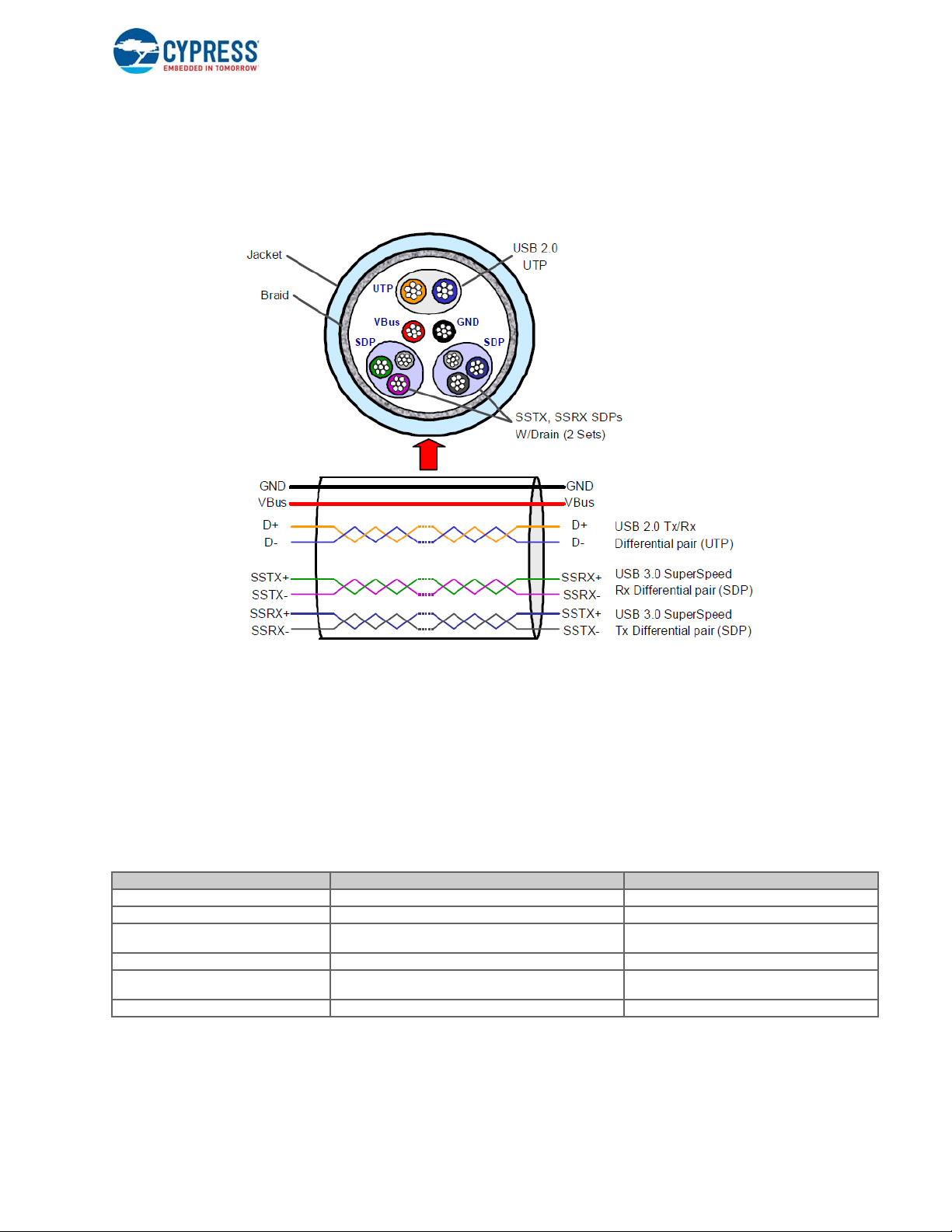
Introduction to EZ-USB FX3
(see Figure 1-1). The SuperSpeed bus employs a dual-simplex approach that allows simultaneous transmission and
reception of packets. In many cases, a SuperSpeed device may be both transmitting and receiving data at the same time. For
example, during burst transactions, a device may be receiving data from the host and returning acknowledgments associated
with the data it already received.
Figure 1-1. Cross-Section of a USB 3.0 Cable
Coming to the power distribution via the USB 3.0 host, 150 mA is considered as the unit load. USB 3.0 host supplies one unit
load of current for unconfigured devices and six unit loads of current for configured devices. The USB 3.0 host detects the
device connection based on the receiver end termination, and the transmitter is responsible for detecting the device
connection. USB 3.0 uses spread-spectrum clocking on its signaling. If spread-spectrum clocking is enabled, then the energy
of the signal is spread over a larger frequency band rather concentrated over a small frequency band at a high level, helping
to reduce the EMI emissions. The USB 3.0 physical layer supports low-frequency periodic signaling (LFPS), which is used to
manage signal initiation and low-power management on the bus on an idle link to consume less power. Ta bl e 1 -1 lists the
differences between the USB 3.0 and USB 2.0 physical layers.
Table 1-1. Differences Between Physical Layers of USB 3.0 and USB 2.0
Feature USB 3.0 USB 2.0
Signaling rate 5 Gbps 480 Mbps
Data transfers Dual simplex Half duplex
Number of pins in the USB cable
Data lines in the cable Shielded differential pair (SDP, twisted, or twinax) Unshielded twisted pair (UTP)
Current supplied by the host
Device detection by the host Receiver end termination Pull-up resistor on D+ or D- lines
9 (VBUS, Ground, D+, D-, SSRX+, SSRX-, SSTX+, SSTX-,
Ground_Drain)
150 mA for unconfigured devices, 900 mA for configured
devices
4 (VBUS, Ground, D+, D-)
100 mA for unconfigured devices, 500 mA for configured devices
1.1.2 Link Layer
The link layer is responsible for maintaining a reliable and robust communication channel between the host and the device.
The Link Training and Status State Machine (LTSSM) at the core of the USB 3.0 link layer establishes the link connectivity
EZ-USB FX3 Technical Reference Manual, Document Number: 001-76074 Rev. *F 20
Page 21

Introduction to EZ-USB FX3
and link power management states and transitions. LTSSM consists of 12 states, including four operational link states (U0,
U1, U2, U3). The link layer offers these four link power states for better power management:
■ U0-Fully powered; link partners are fully powered and ready to send packets
■ U1-Standby with fast recovery; link is in a low-power state and is not ready to send packets but can transition back to U0
within microseconds
■ U2-Standby with slow recovery; link power saving is greater than U1 and transitioning back to U0 within microseconds to
milliseconds
■ U3-Suspend; greatest power savings and longest recovery back to U0 (milliseconds)
■ U1, U2, and U3 have increasingly longer wakeup times into U0 and thus allow transmitters to go into increasingly deeper
sleep.
■ Four link initialization and training states (Rx.Detect, Polling, Recovery, Hot Reset)
■ Two link test states (Loopback and Compliance mode)
■ SS.Inactive (link error state where USB 3.0 is nonoperable)
■ SS.Disabled (SuperSpeed bus is disabled and operates as USB 2.0 only)
Link commands are used to maintain the link flow control and to initiate a change in the link power state.
1.1.3 Protocol Layer
The protocol layer manages the communication rules between a host and device. The SuperSpeed protocol layer includes
the following improvements to enable better performance, efficiency, and power conservation. The information in this section
is provided as background material; the FX3 logic manages protocol details so the application program can deal directly with
USB data.
1.1.3.1 Unicast Transactions
SuperSpeed transactions are routed directly from a root port to the target device with the help of a route string in the packet
header. Therefore, only links in the direct path between the root port and target device see the traffic, which lets other links in
the topology enter or remain in a low-power state.
1.1.3.2 Token/ Data/Handshake Sequences
A USB 2.0 transaction consists of three packets: token, data, and handshake. A transaction is initiated with the token packet
and it is always from the host. Data packets deliver the payload data, which can be sourced by the host or device. The
handshake packet acknowledges the error-free receipt of data and is sent by the receiver of the data. But with SuperSpeed,
to save bandwidth, the token is incorporated into the data packet for OUT transactions; it is replaced by the handshake for IN
transactions. So an ACK packet acknowledges the previous data packet sent and requests the next data packet. The
following examples clarify the differences between USB 2.0 and USB 3.0 IN and OUT transactions.
1.1.3.2.1 IN Transaction Exam ple
Figure 1-2 on page 22 illustrates the differences between USB 2.0 and SuperSpeed OUT transactions. The example on the
left in Figure 1-2 on page 22 shows the sequence of packets required to perform two USB 2.0 IN transactions that require six
packets:
1. Host broadcasts an IN token packet (1) to initiate the transaction.
2. Device returns the requested data packet (2).
3. Host acknowledges receipt of data with an ACK handshake packet (3).
4. Steps 1-3 are repeated.
The example on the right indicates the packet sequence necessary to perform two back-to-back SuperSpeed IN transactions,
which require only five packets to be exchanged:
1. SuperSpeed uses an ACK header (1) to initiate an IN transaction.
2. The SuperSpeed device returns the data packet (2).
EZ-USB FX3 Technical Reference Manual, Document Number: 001-76074 Rev. *F 21
Page 22
Introduction to EZ-USB FX3
Host Controller
High-Speed Device
IN Token
DATA
ACK
IN Token
ACK
DATA
Host Controller
SuperSpeed Device
ACK Header
DATA Header
+ Payload
DATA Header
+ Payload
ACK Header
ACK Header
1
4
6
5
1
3
4
2
3
2
5
3. The second ACK header (3) both acknowledges receipt of the data and requests a second transaction.
4. The second data packet (4) is delivered by the device.
5. The final ACK header (5) acknowledges receipt of the data, but does not request additional data.
Figure 1-2. USB 2.0 IN Transaction Versus USB 3.0 IN Transaction
1.1.3.2.2 OUT Transaction Example
Figure 1-3 illustrates the differences between USB 2.0 and SuperSpeed OUT transactions. The example on the left shows
two back-to-back OUT transactions that require six packets:
1. Host broadcasts an OUT token packet (1) to initiate the transaction.
2. Host sends a data packet (2) to the device.
3. Device acknowledges receipt of data with an ACK handshake packet (3).
4. Steps 1-3 are repeated
The right side of Figure 1-3 shows the packet sequence required to perform two back-to-back SuperSpeed OUT transactions,
requiring only 4 packets to be exchanged:
1. SuperSpeed USB uses a data header (1) to initiate an OUT transaction and to deliver data to the device.
2. Device acknowledges receipt of data via an ACK packet (2).
3. The second data packet (3) initiates the second transaction and delivers data to the device.
4. Device acknowledges receipt of data via an ACK packet (4), completing the sequence.
EZ-USB FX3 Technical Reference Manual, Document Number: 001-76074 Rev. *F 22
Page 23
Introduction to EZ-USB FX3
Host Controller
High-Speed Device
OUT Token
DATA
ACK
OUT Token
DATA
Host Controller
SuperSpeed Device
ACK Header
DATA Header
+ Payload
1
4
5
6
1
3
2
2
ACK
DATA Header
+ Payload
ACK Header
4
3
Figure 1-3. USB 2.0 OUT Transaction Versus USB 3.0 OUT Transaction
1.1.3.3 Data Bursting
The SuperSpeed end-to-end protocol supports transmitting the data in bursts (multiple data packets) without receiving an
acknowledgement to improve latency and performance. The protocol allows efficient bus utilization by concurrently
transmitting and receiving over the bus. A transmitter (host or device) can burst multiple packets of data back to back, and the
receiver can transmit data acknowledgements without interrupting the burst of data packets. Also, the host may
simultaneously schedule multiple OUT bursts to be active at the same time as an IN burst. Devices report their ability to
support bursting in their device descriptors. The maximum burst size is 16, and the actual number to be used represents the
number of data packets that can be sent without receiving an acknowledgement.
This bursting approach is explained in Figure 1-3 with an IN endpoint that supports a burst size of four. The host initiates the
burst transfer and indicates the expected sequence number of the first data packet returned (Seq=0) and the number of
packets it wishes to receive (NumP=4). The target device responds with a burst sequence of four data packets without
receiving any handshakes. A fifth data packet cannot be returned until data packet zero is acknowledged and the host has
indicated a request for another data packet (that is, a second ACK packet with NumP=4). In this burst example, the host
continues to request additional data by keeping the NumP value at 4.
EZ-USB FX3 Technical Reference Manual, Document Number: 001-76074 Rev. *F 23
Page 24
Figure 1-4. Data Bursting in SuperSpeed
ACK Packet
Host TX
Seq = 0; NumP = 4
Device TX
DATA Packet
Seq = 0
DATA Packet
Seq = 1
DATA Packet
Seq = 2
DATA Packet
Seq = 3
ACK Packet
Seq = 1; NumP = 4
ACK Packet
Seq = 4; NumP = 4
Introduction to EZ-USB FX3
1.1.3.4 End-to-End Flow Control
USB 2.0 uses polling and the NAK handshake packet for flow control. For example, USB keyboards must be constantly polled
by the host software to check for activity. When an IN token packet is delivered and no keyboard activity has occurred, the
keyboard returns a NAK packet. Subsequently, the host software will poll the device again and receive another NAK. This
process continues until there is renewed activity. SuperSpeed flow control uses a poll-once approach coupled with an
asynchronous ready notification. Consider the IN transaction shown in Figure 1-5. An ACK packet initiates the IN transaction
and if a device responds with "NRDY" (Not Ready), then the host stops talking to that device until the device sends the
"ERDY" (ready) packet saying that now it is ready to transmit the data. So the host does not need to continue polling. This can
significantly reduce SuperSpeed traffic and improve link power management.
EZ-USB FX3 Technical Reference Manual, Document Number: 001-76074 Rev. *F 24
Page 25
Figure 1-5. End-to-End Flow Control in SuperSpeed
ACK Packet
Host TX
Seq = 0; NumP = 4
Device TX
NRDY Packet
DATA Packet
Seq = 0
ACK Packet
Seq = 1; NumP = 3 (Handshake)
ERDY Packet
ACK Packet
Seq = 0; NumP = 4
Introduction to EZ-USB FX3
1.1.3.5 Streams
USB 3.0 enhanced the bulk transfer capabilities by adding a concept called "streams." This allows a device to accept multiple
commands on a pipe from the host and to complete them out of order using the stream IDs.
Table 1-2 lists the differences between the USB 3.0 and USB 2.0 protocol layers:
Table 1-2. Differences Between USB 3.0 and USB 2.0 Protocol Layers
Bus transaction protocol
Data transfer types
Maximum packet size
Control 512 64
Interrupt 1024 1024
Bulk
Isochronous 1024 1024
1.2 SuperSpeed Power Management
SuperSpeed USB provides a much improved mechanism for entering and exiting low-power states. USB 2.0 implements a
feature known as "Suspend" that forces devices to limit current consumption to 2.5 mA. Entry into the low-power state
requires a minimum of 3 ms, and exit requires more than 20 ms. SuperSpeed power management provides finer granularity
when entering low-power states and reduces entry and exit times. The device can also initiate the low-power link states when
it is idle.
EZ-USB FX3 Technical Reference Manual, Document Number: 001-76074 Rev. *F 25
Feature USB 3.0 USB 2.0
Host directly routes the packet to the targeted device with the help of
route string; exception-isochronous timestamp packet
Asynchronous traffic flow Polled traffic flow
Simultaneous IN/OUTs IN or Out
USB 2.0 types with SuperSpeed constraints; bulk has streams capability
Host broadcasts the packets to all devices-no route
string
Four types: Control, interrupt, bulk, isochronous
1024
Supports streaming functionality Does not support
Page 26

Introduction to EZ-USB FX3
Power management features are implemented at all layers:
The physical layer supports the remote wakeup signaling.
The link layer supports low-power link state entry and exit with the help of LTSSM and link commands. It offers four link power
states (U0, U1, U2, and U3) for better power management. The following architectural features aid in SuperSpeed link power
management:
■ The much higher transmission rates mean that SuperSpeed transactions complete very quickly, leaving links in the idle
state for a longer period of time.
■ The Unicast approach involves only the links in the direct path between the originating root port and target device, leaving
other links idle.
■ The "poll once and notify" mechanism used in SuperSpeed end-to-end flow control reduces overall link traffic.
Protocol layer supports endpoint busy/ready notifications.
1.2.1 Function Power Management
SuperSpeed power management includes the ability to place a specific function (an interface or a set of interfaces) into a
suspended state. This means that a multifunction device can have some functions suspended while others remain fully
operational. Functions are placed into suspend under software control. The asynchronous Function Wake notification tells
software that a suspended function or device is requesting a remote wakeup.
1.3 FX3/FX3S Features
EZ-USB FX3/FX3S supports the following features.
■ Universal Serial Bus (USB) integration
❐ USB 3.0 and USB 2.0 peripherals compliant with USB 3.0 specification revision 1.0
❐ 5-Gbps USB 3.0 PHY
❐ HS-OTG host and peripheral compliant with OTG Supplement version 2.0
❐ 32 physical endpoints
■ General Programmable Interface (GPIF II)*
❐ Programmable GPIF II, enabling connectivity to a wide range of external devices
❐ Interface frequency of up to 100 MHz
❐ 8-, 16-, and 32-bit data bus
❐ As many as 16 configurable control signals
■ 32-bit CPU
❐ ARM926EJ core with 200-MHz operation
❐ 512 KB or 256 KB embedded SRAM
■ Additional connectivity to the following peripherals:
❐ I2C master controller up to 1 MHz
❐ I2S master (transmitter only) at sampling frequencies of 8 kHz, 16 kHz, 32 kHz, 44.1 kHz, 48 kHz, 96 kHz, and
192 kHz
❐ UART support of up to 4 Mbps
❐ SPI master at 33 MHz
■ Selectable clock input frequencies
❐ 19.2, 26, 38.4, and 52 MHz
❐ 19.2-MHz crystal input support
■ Ultra low-power in core power-down mode
❐ Less than 60 μA with VBATT on and 20 μA with VBATT off
EZ-USB FX3 Technical Reference Manual, Document Number: 001-76074 Rev. *F 26
Page 27

Introduction to EZ-USB FX3
❐ Independent power domains for core and interfaces
❐ Core and USB operation at 1.2 V
❐ GPIF II, I2S, UART, and SPI operation at 1.8 to 3.3 V
❐ I2C and JTAG operation at 1.2 to 3.3 V
■ Storage interfaces*
❐ Mass storage support
❐ SD 3.0 (SDXC) UHS-1
❐ eMMC 4.41
❐ Two ports that can support memory card sizes up to 2 TB
❐ Built-in RAID (implemented in firmware) with support for RAID0 and RAID1
■ System I/O expansion with two secure digital I/O (SDIO 3.0) ports
■ Support for USB-attached storage (UAS), mass-storage class (MSC), human interface device (HID), full, and Turbo-
MTP™
*Storage interfaces are available only with FX3S and its GPIF data bus width is limited to 16 bits.
Table 1-3. Feature Differences Between FX3 and FX3S
Feature EZ-USB FX3 EZ-USB FX3S
GPIF 8/16/32-bit 8/16-bit
Storage ports No 1 or 2 ports (SD3.0, eMMC4.41, SDIO3.0)
USB 3.0, USB 2.0 Device Yes Yes
HS-OTG Yes Yes
CPU ARM9, 200 MHz ARM9, 200 MHz
Embedded SRAM 256 KB/512 KB 256 KB/512 KB
Serial Interfaces* I2C, SPI, I2S, UART I2C, SPI, I2S, UART
Boot Options I2C, SPI, USB, GPIF based All FX3 boot options + eMMC based boot options
Package 121-ball BGA, 10 x 10 mm, 0.8 mm pitch 121-ball BGA, 10 x 10 mm, 0.8 mm pitch
*All serial interfaces might not be available under all configuration options. Refer to the pin description section in the
datasheet for details.
EZ-USB FX3 Technical Reference Manual, Document Number: 001-76074 Rev. *F 27
Page 28

1.3.1 FX3 Block Diagram
32
EPs
GPIF II
SS
Peripheral
HS/FS/LS
OTGHost
JTAG
UART SPI
CTL[15:0]
INT#
RESET#
TDI
TDO
TRST#
TMS
TCK
DQ[31:0]/[15:0]
PMODE[2:0]
SSRX +
SSRX SSTX +
SSTX -
D +
D -
FSLC[0]
FSLC[1]
FSLC[2]
CLKIN
CLKIN_32
XTALIN
XTALOUT
OTG_ID
I2SI2C
SRAM
(512kB/256kB)
ARM9
USB
HS/FS
Peripheral
DMA Interconnect
I2C_SCL
I2C_SDA
TX
RX
CTS
RTS
SSN
SCLK
MISO
MOSI
I2S_CLK
I2S_SD
I2S_WS
I2S_MCLK
Introduction to EZ-USB FX3
Figure 1-6. FX3 Block Diagram
EZ-USB FX3 Technical Reference Manual, Document Number: 001-76074 Rev. *F 28
Page 29
1.3.2 FX3S Block Diagram
32
EPs
GPIF II
SS
Peripheral
HS/FS/LS
OTGHost
JTAG
UART
SPI
CTL[15:0]
INT#
RESET#
TDI
TDO
TRST#
TMS
TCK
DQ[15:0]
PMODE[2:0]
SSRX +
SSRX SSTX +
SSTX -
D +
D -
FSLC[0]
FSLC[1]
FSLC[2]
CLKIN
CLKIN_32
XTALIN
XTALOUT
OTG_ID
I2S
I2C
SRAM
(512kB/256kB)
ARM9
USB
HS/FS
Peripheral
DMA
Interconnect
I2C_SCL
I2C_SDA
S1_CMD
S1_WP
S1_D[7:0]
SD/MMC controller
S0-port S1-port
S1_CLK
S0_CLK
S0_CMD
S0_WP
S0_D[7:0]
S0S1_INS
Introduction to EZ-USB FX3
Figure 1-7. FX3S Block Diagram
Note: For more details on pin mapping and their descriptions, refer to FX3 and FX3S datasheets.
1.4 Functional Overview
1.4.1 CPU
FX3 has an on-chip 32-bit, 200-MHz ARM926EJ-S core CPU. The core has direct access to 16 KB of instruction tightly
coupled memory (TCM) and 8 KB of data TCM. The ARM926EJ-S processor also has associated instruction cache (I-cache)
and data cache (D-cache) memories. Both the instruction and data caches are 8 KB.
FX3 integrates 512 KB or 256 KB (depending on the part number) of embedded SRAM for storing code and data. The
ARM926EJ-S core provides a JTAG interface for firmware debugging.
FX3 interrupts are managed through the standard ARM PrimeCell Vectored Interrupt Controller (PL192) block. This interrupt
controller provides vectored interrupt support with configurable priorities for all interrupt sources.
Examples of the FX3 firmware are available with the Cypress EZ-USB FX3 Development Kit.
For more information about the CPU subsystem, refer to the FX3 CPU Subsystem chapter on page 34.
For more information about the memory map, refer to the Memory and System Interconnect chapter on page 44.
EZ-USB FX3 Technical Reference Manual, Document Number: 001-76074 Rev. *F 29
Page 30

Introduction to EZ-USB FX3
1.4.2 DMA
FX3 enables efficient and flexible DMA transfers between the various peripherals (such as USB, GPIF II, I2S, SPI, and
UART), requiring firmware only to configure data accesses between peripherals. The data transfers are managed by
distributed DMA controllers within each peripheral. For more information about the FX3 DMA interconnect, refer to the FX3
DMA Subsystem chapter on page 58.
1.4.3 USB Interface
The FX3 USB interface supports the following:
■ USB SuperSpeed and High-Speed peripheral functionality is compliant with USB 3.0 specification revision 1.0 and is
backward compatible with the USB 2.0 specification.
■ As a USB peripheral, FX3 supports SuperSpeed, High-Speed, and Full-Speed transfers. As a host, FX3 supports High-
Speed, Full-Speed, and Low-Speed transfers.
■ Complies with OTG Supplement revision 2.0, supporting dual-role operation. As an OTG host, FX3 supports
■ USB classes such as Mass Storage (MSC) and Human Interface Device (HID).
■ Carkit Pass-through UART functionality on USB D+/D- lines based on the CEA-936A specification
■ 16 IN and 16 OUT endpoints
■ CONTROL, BULK, INTERRUPT, and ISOCHRONOUS endpoints
■ USB 3.0 BULK streams feature
For more information about the USB block, refer to the Universal Serial Bus (USB) chapter on page 78.
1.4.4 GPIF II
The GPIF II is a programmable state machine that enables a flexible interface that may function either as a master or slave to
industry-standard or proprietary interfaces. The high-performance GPIF II interface provides functionality similar to, but more
advanced than, the FX2LP™ GPIF and Slave FIFO interfaces. Both parallel and serial interfaces may be implemented with
GPIF II.
The GPIF II implements an interface by creating a GPIF II state machine. GPIF II state transitions are based on input signals,
and the control output signals are driven as a result of the GPIF II state transitions. Some popular interfaces that can be
implemented with GPIF II are the Slave FIFO interface, SRAM, Address/Data bus interfaces, and Address Multiplexed
(ADMux) interfaces.
For more information about the synchronous Slave FIFO interface, refer to the application note AN65974 - Designing with the
EZ-USB FX3 Slave FIFO Interface.
The key features of GPIF II are:
■ Functions as a master or slave
■ Provides 256 firmware programmable states
■ Supports 8-bit, 16-bit, 24-bit, and 32-bit parallel data buses
■ Enables interface frequencies up to 100 MHz
■ Supports 14 configurable control pins when a 32-bit data bus is used. All control pins can be either input or outputor bidi-
rectional.
■ Supports 16 configurable control pins when a 16- or 8-bit data bus is used. All control pins can be either input or output or
bidirectional.
Cypress's GPIF II Designer tool enables GPIF II designs to be developed quickly and includes examples of common
interfaces. For more information about the GPIF II block, refer to the General Programmable Interface II (GPIF II) chapter on
page 120.
EZ-USB FX3 Technical Reference Manual, Document Number: 001-76074 Rev. *F 30
Page 31

Introduction to EZ-USB FX3
1.4.5 UART Interface
FX3 UART supports full-duplex communication and consists of the TX, RX, CTS, and RTS signals. The UART is capable of
generating a range of baud rates, from 300 bps to 4608 Kbps, selectable by the firmware. If flow control is enabled, then the
FX3 UART transmits data when the CTS input is asserted. In addition, the FX3 UART asserts the RTS output signal when it is
ready to receive data.
1.4.6 I2C Interface
The FX3 I2C interface is compatible with the I2C Bus Specification revision 3. This I2C interface is capable of operating only
as an I2C master; therefore, it may be used to communicate with other I2C slave devices. For example, FX3 may boot from
an EEPROM connected to the I2C interface, as a selectable boot option.
The FX3 I2C master controller also supports multimaster functionality. The FX3 I2C controller is powered by a dedicated
power pin, VIO5, which also powers the JTAG interface. This gives the I2C interface the flexibility to operate at a different
voltage than other serial interfaces.
The I2C controller supports bus frequencies of 100 kHz, 400 kHz, and 1 MHz. When VIO5 is 1.2 V, the maximum operating
frequency is 100 kHz. When VIO5 is 1.8 V, 2.5 V, or 3.3 V, the operating frequencies supported are 400 kHz and 1 MHz. The
I2C controller supports the clock-stretching feature to enable slower devices to exercise flow control. The I2C interface's SCL
and SDA signals require external pull-up resistors, which must be connected to VIO5.
1.4.7 I2S Interface
FX3 has an I2S port to support external audio codec devices. FX3 functions as an I2S master as a transmitter only.
The I2S interface consists of four signals: clock (I2S_CLK), serial data (I2S_SD), word select (I2S_WS), and master system
clock (I2S_MCLK). FX3 can generate the system clock as an output on I2S_MCLK or accept an external system clock input
on I2S_MCLK.
The I2S master (transmitter only) supports sampling frequencies of 8 kHz, 16 kHz, 32 kHz, 44.1 kHz, 48 kHz, 96 kHz, and
192 kHz.
1.4.8 SPI Interface
FX3 provides an SPI master interface. The maximum operation frequency is 33 MHz. The SPI controller supports four modes
of SPI communication. This controller is a single master controller with a single automated Slave Select, Negative-true (SSN)
control. It supports transaction sizes ranging from 4 bits to 32 bits.
For more information about the UART, I2C, I2S, and SPI interfaces, refer to the Low Performance Peripherals (LPP) chapter
on page 167.
1.4.9 JTAG Interface
The FX3 JTAG interface is a standard five-pin interface to connect to a JTAG debugger to debug the firmware through the
CPU core's on-chip-debug circuitry. Industry-standard debugging tools for the ARM926EJ-S core can be used for FX3
application development.
1.4.10 Storage Interface
FX3S has two independent storage ports (S0-Port and S1-Port). Both storage ports support the following specifications:
■ MMC system specification, MMCA Technical Committee, version 4.41
■ SD specification, version 3.0
■ SDIO host controller compliant with SDIO Specification version 3.00
Both storage ports support the following features:
EZ-USB FX3 Technical Reference Manual, Document Number: 001-76074 Rev. *F 31
Page 32

Introduction to EZ-USB FX3
1.4.10.1 SD/MMC Clock Stop
FX3S supports the stop clock feature, which can save power if the internal buffer is full when receiving data from the SD/
MMC/SDIO.
1.4.10.2 SD_CLK Output Clock Stop
During the data transfer, the SD_CLK clock can be enabled (on) or disabled (stopped) at any time by the internal flow control
mechanism.
SD_CLK output frequency is dynamically configurable using a clock divider from a system clock. The clock choice for the
divisor is user-configurable through a register. For example, the following frequencies may be configured:
■ 400 kHz - For the SD/MMC card initialization
■ 20 MHz - For a card with 0- to 20-MHz frequency
■ 24 MHz - For a card with 0- to 26-MHz frequency
■ 48 MHz - For a card with 0- to 52-MHz frequency (48-MHz frequency on SD_CLK is supported when the clock input to
FX3S is 19.2 MHz or 38.4 MHz)
■ 52 MHz - For a card with 0- to 52-MHz frequency (52-MHz frequency on SD_CLK is supported when the clock input to
FX3S is 26 MHz or 52 MHz)
■ 100 MHz - For a card with 0- to 100-MHz frequency If the DDR mode is selected, data is clocked on both the rising and
falling edge of the SD clock. DDR clocks run up to 52 MHz.
1.4.10.3 Card Insertion and Removal Detection
FX3S supports the following two card insertion and removal detection mechanisms:
■ Use of SD_D[3] data
■ Use of the S0S1_INS pin
1.4.10.4 Write Protection (WP)
The S0_WP/S1_WP (SD Write Protection) on S-Port is used to connect to the WP microswitch of the SD/MMC card
connector. This pin internally connects to a CPU-accessible GPIO for firmware to detect the SD card write protection.
1.4.10.5 SDIO Interrupt
The SDIO interrupt functionality is supported as specified in the SDIO specification version 2.00 (January 30, 2007).
1.4.10.6 SDIO Read-Wait Feature
FX3S supports the optional read-wait and suspend-resume features as defined in the SDIO specification version 2.00
(January 30, 2007).
1.4.10.7 Boot Options
FX3 integrates 32 KB of ROM, which contains a bootloader, allowing FX3 to load boot images from various sources. The boot
mode is selected by the configuration of the PMODE pins as shown in Table 1-3 on page 27
The FX3 boot options are:
■ Boot from USB
■ Boot from I2C
■ Boot from SPI
■ Boot from GPIF II Async ADMux mode
■ Boot from GPIF II Sync ADMux mode
■ Boot from GPIF II Async SRAM mode
EZ-USB FX3 Technical Reference Manual, Document Number: 001-76074 Rev. *F 32
Page 33

Refer to the application note AN76405 - EZ-USB FX3 Boot Options.
In addition to these FX3 boot options, FX3S supports the following:
■ Boot from eMMC (Storage port)
■ Boot from PMMC (Processor port)
Table 1-4. Boot Mode Selection Based on PMODE Pins
PMODE[2:0] Pins Boot Option
PMODE[2] PMODE[1] PMODE[0]
Z 0 0 Sync ADMUX (16-bit)
Z 0 1 Async ADMUX (16-bit)
Z 0 Z Async SRAM (16-bit)
Z 1 1 USB Boot
1ZZ I2C
Z 1 Z I2C; on failure, USB Boot is enabled
0 Z 1 SPI; on failure, USB Boot is enabled
FX3S Specific Boot Options
Z 1 0 PMMC Legacy
0 0 0 S0-port (eMMC); On Failure, USB Boot is enabled
1 0 0 S0-port (eMMC)
Introduction to EZ-USB FX3
Z = Pin is floating; left unconnected.
1.4.11 Clocking
FX3 allows either connecting a crystal between the XTALIN and XTALOUT pins or connecting an external clock to the CLKIN
pin. The XTALIN, XTALOUT, CLKIN, and CLKIN_32 pins can be left unconnected if they are not used.
The crystal frequency supported is 19.2 MHz, while the external clock frequencies supported are 19.2, 26, 38.4, and 52 MHz.
FX3 has an on-chip oscillator circuit that uses an external 19.2-MHz (±100 ppm) crystal (when the crystal option is used).
Refer to the application note AN70707 - EZ-USB FX3/FX3S Hardware Design Guidelines and Schematic Checklist for
guidelines on crystal selection. An appropriate load capacitance is required with a crystal. The FSLC[2:0] pins must be
configured appropriately to select the crystal- or clock-frequency option. The configuration options are listed in Table 1-4.
Table 1-5. Crystal and Clock Frequency Selection
FSLC[2] FSLC[1] FSLC[0] Crystal/Clock Frequency
0 0 0 19.2-MHz Crystal
1 0 0 19.2-MHz Input CLK
1 0 1 26-MHz Input CLK
1 1 0 38.4-MHz Input CLK
1 1 1 52-MHz input CLK
Clock inputs to FX3 must meet the phase noise and jitter requirements specified in the EZ-USB FX3 datasheet.
EZ-USB FX3 Technical Reference Manual, Document Number: 001-76074 Rev. *F 33
Page 34

2. FX3 CPU Subsystem
The EZ-USB FX3 device has an embedded 32-bit ARM926EJ-S core that delivers a processing capability up to 220 MIPS.
This ARM core is coupled with instruction and data caches, Tightly Coupled Memories (TCM), and a PL192 vectored interrupt
controller (VIC). FX3 also implements the standard ARM JTAG Test Access Point (TAP), which allows you to use standard
JTAG debuggers to debug firmware applications.
The ARM926EJ-S processor is targeted at multitasking applications and can support high-performance and low-power
requirements.
Interrupts in the FX3 device are managed through the standard ARM PL192 VIC block.
2.1 Features
The ARM9 core in the FX3 device supports the following features:
■ Operation at frequencies up to 200 MHz
■ Support for both 32-bit ARM and 16-bit thumb instructions
■ Integrated data and instruction caches of 8 KB each
■ Dedicated instruction and data TCMs for guaranteed low-latency memory access
■ VIC capable of managing 32 internal interrupt sources with programmable interrupt priorities
■ Standard ARM JTAG interface for debugging
■ Clock frequency control for power saving
■ System RAM on FX3 device serves as main storage for code and data
EZ-USB FX3 Technical Reference Manual, Document Number: 001-76074 Rev. *F 34
Page 35

2.2 Block Diagram
Instruction
Cache
(8 KB)
Data
Cache
(8 KB)
ARM926EJ-S Core
AHB Bridge
Instruction AHB
(32 bit x 200 MHz)
Data AHB
(32 bit x 200 MHz)
FX3 System Interconnect (AHB)
PL192
VIC
nIRQ
nFIQ
Interrupt
Requests
ITCM
(16 KB)
DTCM
(8 KB)
Single Cycle ARM TCM Access
(32 bit x 200 MHz)
JTAG
TAP
JTAG
Interface
FX3 CPU Subsystem
Figure 2-1. CPU Subsystem in FX3 Device
2.3 Functional Overview
Figure 2-1 shows the ARM9 core and the associated blocks in the FX3 device. The CPU is associated with TCM blocks that
enable zero-latency accesses to performance-critical instructions and data, and it provides separate instruction and data
caches for other memory accesses. The PL192 VIC manages interrupts raised by the FX3 hardware blocks.
2.3.1 ARM926EJ-S CPU
The FX3 device has an embedded 32-bit ARM926EJ-S CPU core. This makes the device capable of implementing
multitasking applications where high performance and low power consumption are important.
This ARM9 core supports both 32-bit ARM instructions and 16-bit thumb instructions. The processor has separate advanced
high-performance bus (AHB) interfaces for internal instruction and data accesses. It also has separate instruction and data
TCM interfaces.
Note: The 32-bit ARM instruction set is commonly used in the FX3 SDK from Cypress, as this makes it more convenient to
address all of the available device memory.
EZ-USB FX3 Technical Reference Manual, Document Number: 001-76074 Rev. *F 35
Page 36

FX3 CPU Subsystem
The following subsections provide information for programming the FX3 device. The FX3 SDK takes care of these aspects
and initializes the ARM core and memory blocks on the FX3 device. The following detail is only required if you are making any
modifications to the base SDK source code. For more details on the ARM CPU architecture, instruction set, and so on, refer
to the
ARM926EJ-S Technical Reference Manual.
2.3.1.1 Processor Modes
The ARM architecture supports seven operating modes, as shown in Table 2-1.
Table 2-1. ARM9 CPU Operating Modes
Processor Mode Abbreviation Description
User Usr Normal program execution mode
FIQ Fiq Fast interrupt mode; used for a performance-critical interrupt
IRQ Irq General-purpose interrupt handling mode
Supervisor Svc Protected mode used by operating systems
Abort Abt Instruction/data abort handling mode; used for virtual memory implementation
Undefined Und
System Sys Runs privileged operating system tasks
All of the modes except the user mode are privileged modes that have full access to all system resources and can freely
change modes.
Undefined instruction mode; used to support software emulation of hardware coprocessors; generally not useful
on FX3 device.
The FIQ, IRQ, supervisor, abort, and undefined modes are entered when specific exceptions occur. These modes have a
separate register set, so that the user mode registers are not corrupted when the exception occurs.
The system mode uses the same set of registers as the user mode and is used to execute OS tasks that do not need a
separate register set.
Run-time stack regions need to be set up for all these modes at system startup. The following code snippet shows how this
can be done using ARM assembly language code. This code is provided by the Cypress FX3 firmware library, and rarely
needs to be modified.
#define FX3_STACK_BASE 0x10000000 /* D-TCM area ( 8KB ) */
#define FX3_SVC_STACK_SIZE 0x1000 /* SVC stack size */
#define FX3_FIQ_STACK_SIZE 0x0200 /* FIQ stack size */
#define FX3_IRQ_STACK_SIZE 0x0400 /* IRQ stack size */
#define FX3_SYS_STACK_SIZE 0x0800 /* SYS stack size */
#define FX3_ABT_STACK_SIZE 0x0100 /* ABT stack size */
#define FX3_UND_STACK_SIZE 0x0100 /* UND stack size */
#define ARM_FIQ_MODE 0xD1 /* Disable Interrupts + FIQ mode */
#define ARM_IRQ_MODE 0xD2 /* Disable Interrupts + IRQ mode */
#define ARM_SVC_MODE 0xD3 /* Disable Interrupts + SVC mode */
#define ARM_ABT_MODE 0xD7 /* Disable Interrupts + ABT mode */
#define ARM_UND_MODE 0xDB /* Disable Interrupts + UND mode */
#define ARM_SYS_MODE 0xDF /* Disable Interrupts + SYS mode */
/* Stack pointers are placed at the top address as the stack grows downwards */
SetupStackPtrs:
ldr r1, =FX3_STACK_BASE /* Load the stack base address */
sub r1, r1, #8 /* Prevent overflow */
ldr r2, =FX3_SYS_STACK_SIZE /* Pickup stack size */
mov r3, #ARM_SYS_MODE /* Build SYS mode CPSR */
msr CPSR_cxsf, r3 /* Enter SYS mode */
add r1, r1, r2 /* Calculate start of SYS stack */
EZ-USB FX3 Technical Reference Manual, Document Number: 001-76074 Rev. *F 36
Page 37

bic r1, r1, #7 /* Ensure 8-byte alignment */
mov sp, r1 /* Setup SYS stack pointer */
mov r10, #0 /* Clear SYS mode sl */
mov r11, #0 /* Clear SYS fp */
ldr r2, =FX3_ABT_STACK_SIZE /* Pickup stack size */
mov r3, #ARM_ABT_MODE /* Build ABT mode CPSR */
msr CPSR_cxsf, r3 /* Enter ABT mode */
add r1, r1, r2 /* Calculate start of ABT stack */
bic r1, r1, #7 /* Ensure 8-byte alignment */
mov sp, r1 /* Setup ABT stack pointer */
mov r10, #0 /* Clear ABT mode sl */
mov r11, #0 /* Clear ABT fp */
ldr r2, =FX3_UND_STACK_SIZE /* Pickup stack size */
mov r3, #ARM_UND_MODE /* Build UND mode CPSR */
msr CPSR_cxsf, r3 /* Enter UND mode */
add r1, r1, r2 /* Calculate start of UND stack */
bic r1, r1, #7 /* Ensure 8-byte alignment */
mov sp, r1 /* Setup UND stack pointer */
mov r10, #0 /* Clear UND mode sl */
mov r11, #0 /* Clear UND fp */
ldr r2, =FX3_FIQ_STACK_SIZE /* Pickup stack size */
mov r0, #ARM_FIQ_MODE /* Build FIQ mode CPSR */
msr CPSR_c, r0 /* Enter FIQ mode */
add r1, r1, r2 /* Calculate start of FIQ stack */
bic r1, r1, #7 /* Ensure 8-byte alignment */
mov sp, r1 /* Setup FIQ stack pointer */
mov sl, #0 /* Clear sl */
mov fp, #0 /* Clear fp */
FX3 CPU Subsystem
ldr r2, =FX3_IRQ_STACK_SIZE /* Pickup IRQ stack size */
mov r0, #ARM_IRQ_MODE /* Build IRQ mode CPSR */
msr CPSR_c, r0 /* Enter IRQ mode */
add r1, r1, r2 /* Calculate start of IRQ stack */
bic r1, r1, #7 /* Ensure 8-byte alignment */
mov sp, r1 /* Setup IRQ stack pointer */
ldr r2, =FX3_SVC_STACK_SIZE /* Pickup System stack size */
mov r0, #ARM_SVC_MODE /* Build SVC mode CPSR */
msr CPSR_c, r0 /* Enter SVC mode */
add r1, r1, r2 /* Calculate start of SVC stack */
bic r1, r1, #7 /* Ensure 8-byte alignment */
mov sp, r1 /* Setup SVC stack pointer */
Hint: The 8-KB D-TCM region can be used for the run-time stack regions if there is no other performance-critical data that
needs to be placed there.
2.3.1.2 Processor Registers
Table 2-2 shows the registers provided by the ARM9 processor core. The CPSR register is used to switch between various
processor modes.
EZ-USB FX3 Technical Reference Manual, Document Number: 001-76074 Rev. *F 37
Page 38

FX3 CPU Subsystem
Table 2-2. ARM9 Processor Registers
Register Description Attributes
R0-R7 General-purpose registers
R8-R12 General-purpose registers
R13 Stack pointer (SP)
R14
R15 Used to read/write the program counter Single register that is used across all processor modes.
CPSR
SPSR
Link register (LR), used to hold return address when executing branch instructions
Current program status register, provides status flags,
global interrupt enable control, and so on
Saved program status register, provides saved program status for each exception mode
These are not banked registers, which means that the same physical register is
used in all processor modes.
Two copies of these registers exist. One copy is used only in FIQ mode, and the
other copy is used in all other processor modes.
Six copies of this register exist. The user and system modes share one register,
and all other modes have their own SP register.
Six copies of this register exist. The user and system modes share one register,
and all other modes have their own LR register.
The CPSR register reflects the current program status in each of the processor
modes.
Separate copies of this register exist for each of the FIQ, IRQ, supervisor, abort,
and undefined modes.
2.3.1.3 Exception Vectors
The exception vectors that serve as the entry point for each of the exception modes are stored in a table in the main system
memory. These vectors can be placed at one of two addresses: 0x00000000 or 0xFFFF0000. The selection of the exception
vector table location is based on the ARM standard system control coprocessor (CP15) configuration.
As shown in Table 2-3, the normal exception vectors are located in the address range from 0x0 onward, which falls in the
instruction TCM (ITCM) region. The high exception vectors are located in the address range from 0xFFFF0000, which is part
of the BootROM on the FX3 device. As the high-exception vectors are hard-wired to vector to the bootloader on the FX3
device, the normal (user-definable) exception vectors are used when running user applications.
Table 2-3. ARM Exception Vector Locations
Exception Type Processor Mode Exception Vector 1 (normal) Exception Vector 2 (high)
Reset Supervisor 0x00000000 0xFFFF0000
Undefined instruction Undefined 0x00000004 0xFFFF0004
Software interrupt (SWI) Supervisor 0x00000008 0xFFFF0008
Prefetch abort Abort 0x0000000C 0xFFFF000C
Data abort Abort 0x00000010 0xFFFF0010
IRQ (interrupt) IRQ 0x00000018 0xFFFF0018
FIQ (interrupt) FIQ 0x0000001C 0xFFFF001C
The following code snippet shows the procedure to move the exception vectors to address 0x0. This step is done by the FX3
firmware library as part of device initialization.
MRC p15, 0, r1, c1, c0, 0/* Read the CP15 register value */
MOV r2, #0xFFFFDFFF
AND r1, r1, r2/* Mask off the vector location bit. */
MCR p15, 0, r1, c1, c0, 0/* Write back to CP15 register. */
2.3.1.4 MMU
The MMU in the ARM926EJ-S processor is an ARM architecture v5 implementation, which supports the virtual memory
features required by standard embedded operating systems. The MMU uses a set of two-level page tables located in the
main memory to control the address translation, permission checks, and so on.
The data cache on the ARM core can be enabled only if the MMU is enabled. However, most FX3 designs do not use any
secondary storage and do not need a virtual memory system. FX3 provides a fixed set of page tables that maps each physical
address to the equivalent virtual address.
EZ-USB FX3 Technical Reference Manual, Document Number: 001-76074 Rev. *F 38
Page 39

FX3 CPU Subsystem
2.3.1.5 Cache Memories
The ARM926EJ-S processor has associated instruction and data cache memories. The RAM on the FX3 device holds DMA
data buffers in addition to code and data. The DMA driver and APIs in the FX3 library ensure cache coherency by using the
cache clean and invalidate operations.
The instruction and data caches on FX3 are 8 KB. The caches are four-way set associative with eight word (32-byte) cache
lines. The data cache implements two dirty bits per cache line and is typically configured for write-back operations.
The ARM926EJ-S processor supports the following operations using the CP15 coprocessor interface:
■ Invalidating the entire D-cache or I-cache
■ Invalidating (flushing) regions of the D-cache or I-cache
■ Cleaning the entire D-cache
■ Cleaning regions of the D-cache
■ Locking specified memory regions into the D-cache or I-cache
The CPU also provides a write buffer that is used for writes to regions that are not cacheable or bufferable, and for writethrough operations. It is also used for write misses during write-back operations. A separate write buffer is provided as part of
the D-cache for holding write-back data during cache line eviction or clean operations. Instructions are provided to drain both
write buffers, and the CPU ensures data coherency when read operations are addressed to data that is sitting in the write
buffer.
The following code snippet shows the procedure to enable the caches and the MMU on the FX3 device. Refer to the Memory
and System Interconnect chapter on page 44 for more information on cache operations.
MRC p15, 0, r1, c1, c0, 0/* Read CP15 register value */
ORR r1, r1, #0x1000/* Update I-Cache enable bit. */
BIC r1, r1, #0x4000/* Select random replacement. */
ORR r1, r1, #0x05/* Enable MMU and D-Cache. */
MCR p15, 0, r1, c1, c0, 0/* Write modified value back */
2.3.1.6 Tightly Coupled Memories
Some operations, such as interrupt handlers, may not be able to tolerate the added latency created by a cache miss. The
ARM9 CPU provides a zero wait state TCM interface to facilitate quick access to such instructions and data. Firmware
applications can locate performance-critical code and data sections in the TCM regions using the appropriate linker settings.
The FX3 SDK provides a linker script that sets up the recommended memory map for FX3 applications.
As in memory and cache access, separate paths are used for instruction and data access from the TCMs. FX3 implements 16
KB of instruction TCM (ITCM) and 8 KB of data TCM (DTCM). The ITCM area can also be accessed by the data side of the
ARM core. This is required to facilitate loading the code into the ITCM region.
The ITCM region on FX3 is located in the address range 0x0000-0x3FFF, and the DTCM region is located in the address
range 0x10000000-0x10001FFF. The ITCM region is typically used to store the ARM exception vectors and the interrupt
service routine (ISR) code. The DTCM region is typically used to store performance-critical data and the run-time stacks for
various processor modes.
The TCMs must be configured as non-cacheable memories, and any instruction or data movement between the TCM and the
main memory must be performed by the CPU. The TCMs are disabled when the device is reset, and they need to be enabled
by the firmware. This is done by the FX3 library as part of device initialization.
MOV r1, #0x15 /* ITCM address is 0x0 and size is 16 KB. */
MCR p15, 0, r1, c9, c1, 1 /* Initialize the ITCM */
MOV r1, 0x10000011 /* DTCM address is 0x10000000 and size is 8 KB. */
MCR p15, 0, r1, c9, c1, 0 /* Initialize the DTCM */
EZ-USB FX3 Technical Reference Manual, Document Number: 001-76074 Rev. *F 39
Page 40

FX3 CPU Subsystem
2.3.1.7 JTAG Interface
FX3 makes the standard ARM JTAG TAP available for users to connect a JTAG debugger. Only the 5-pin JTAG mode of
debugging is supported, and 2-pin serial wire debug (SWD) mode is not supported by the FX3 device. The JTAG pins are
directly connected to the ARM CPU, and they do not support boundary scan.
The JTAG interface allows the use of industry-standard ARM debug probes to debug the firmware running on FX3. No
Cypress custom software tools are required to enable the debugging.
The JTAG instruction register (IR) length for the ARM926EJ-S device is 4 bits. If multiple devices are connected on the JTAG
chain, the offset and length for the FX3 device have to be set correctly to achieve JTAG connection. Refer to Section 5.10.3 of
the Segger J-Link User Guide for instructions on how to do this when using the J-Link debugger.
2.3.1.8 Vectored Interrupt Controller
The FX3 device provides a number of interrupt notifications for the ARM CPU to handle. Interrupts in the FX3 system are
managed through the standard ARM PrimeCell Vectored Interrupt Controller (PL192) block. This interrupt controller provides
vectored interrupt support with configurable priorities for all interrupt sources.
The PL192 controller supports up to 32 interrupt sources and generates the nIRQ and nFIQ signals to the ARM CPU based
on the configuration. The controller is connected to the CPU on the AHB bus and allows you to perform the interrupt
configuration through a set of memory mapped registers.
Table 2-4 shows the various interrupt sources on the FX3 device, along with their vector numbers.
EZ-USB FX3 Technical Reference Manual, Document Number: 001-76074 Rev. *F 40
Page 41

Table 2-4. FX3 Interrupt Sources
FX3 CPU Subsystem
Vector
Number
0 GCTL_CORE
1 SW_INTR Software interrupt
2 UNUSED Do not enable.
3 UNUSED Do not enable.
4 WATCHDOG_TIMER
5 UNUSED Do not enable.
6 GPIF_DMA DMA socket interrupt from the GPIF block
7 GPIF_CORE
8 USB_DMA DMA socket interrupt from the USB block
9 USB_CORE
10 UNUSED Do not enable.
11 STORAGE_DMA DMA socket interrupt from the storage (SD/MMC) interface Applies only to the FX3S™ devices.
12 STORAGE0_CORE General-purpose interrupt from storage interface 0 Applies only to the FX3S™ devices.
13 STORAGE1_CORE General purpose interrupt from storage interface 1. Applies only to the FX3S™ devices.
14 UNUSED Do not enable.
15 I2C_CORE
16 I2S_CORE General-purpose I2S interrupt
17 SPI_CORE General-purpose SPI interrupt
18 UART_CORE General-purpose UART interrupt
19 GPIO_CORE
20 PERIPH_DMA
21 GCTL_POWER
22-31 UNUSED Do not enable.
Interrupt Source Description Comments
Interrupt raised on FX3 waking up from suspend or standby
low-power modes.
This is a custom implementation of the software
interrupt scheme.
Watchdog timer interrupt; the watchdog timer functions on
the basis of a 32-kHz clock signal with a user-configured
period
General-purpose GPIF interrupts; indicates conditions such
as state machine interrupt, GPIF errors, mailbox register
access, and so on
General-purpose USB interrupts; indicates various conditions triggered during device or host operation of the USB
block
General-purpose I2C interrupt; indicates conditions such as
transfer completion, error detect, and so on
General-purpose GPIO interrupt; common for both simple
and complex GPIOs
DMA socket interrupt from any serial peripheral block (I2C,
I2S, SPI, or UART).
Power detect interrupt; indicates voltage changes on any
power inputs that can be dynamically changed during
device operation.
This is commonly used for OS scheduling on the
FX3 device.
Applies to both USB device and host mode operation.
This is commonly used for VBus voltage detection.
You can configure any of the 32 interrupt sources as fast interrupt request (FIQ), which takes the highest priority among the
interrupts. The rest of the interrupts are prioritized by user code through the VIC_VECT_PRIORITY registers. If two or more
interrupts are programmed with the same priority value, the source with the lower vector number assumes the higher priority.
The PL192 controller allows each of the interrupt sources to be independently masked (disabled) or unmasked (enabled) and
provides registers that report the raw interrupt status and the interrupt status after masking. The vector addresses for various
interrupt sources are programmed through the VIC_VEC_ADDRESS registers. When one or more interrupt sources are
active, the controller identifies the highest priority interrupt, stores the corresponding vector address in the VIC_ADDRESS
register, and then asserts the nIRQ signal to interrupt the ARM CPU.
Refer to Vectored Interrupt Controller (VIC) Registers on page 230 on for information about the various configuration and
status registers associated with the VIC.
Some interrupts in the FX3 system need to be prioritized over others to ensure that the application can meet all the USB spec
requirements and transfer rates. In particular, the USB core interrupt must be handled at the highest priority (can be selected
as FIQ), and all the DMA interrupts should be allotted the next high priority level.
To enable a specific interrupt source, the firmware has to do the following:
■ Point the VIC_VEC_ADDRESS register to the ISR.
EZ-USB FX3 Technical Reference Manual, Document Number: 001-76074 Rev. *F 41
Page 42

FX3 CPU Subsystem
■ Set the VIC_VECT_PRIORITY register value as desired.
■ Enable the interrupt by setting the corresponding bit in the VIC_INT_ENABLE register.
The following code snippet shows the procedure for setting up Fx3IntHandler as the ISR for interrupt vector i:
CY_U3P_VIC_VEC_ADDRESS[i] = Fx3IntHandler;/* ISR address. */
CY_U3P_VIC_VECT_PRIORITY[i] = 2;/* Set the priority to 2. */
CY_U3P_VIC_INT_ENABLE |= (1 << i);/* Enable the interrupt. */
The VIC sets the VIC_ADDRESS register to point to the vector for the active interrupt with the highest priority before making
the nIRQ signal active. The IRQ exception vector is designed to jump to the address pointed by the VIC_ADDRESS register.
The ISR is responsible for saving all the necessary context information, including the non-banked registers, while executing.
Nesting of interrupts is not allowed by the VIC. The ISR needs to clear the interrupt by writing any value to the
VIC_ADDRESS register before the next interrupt can be raised.
As direct interrupt nesting is not supported by the VIC, it is recommended that the handling of low-priority interrupts be
deferred to allow higher priority interrupts to run with bounded latency. The firmware needs to mask out the deferred interrupts
until the source of the interrupt has been cleared to avoid repeated interrupt calls. This can be done by setting the
corresponding bit in the VIC_INT_CLEAR register.
CY_U3P_VIC_INT_CLEAR = (1 << i);/* Mask out interrupt vector i. */
Note:
The ARM CPU uses the ARM instruction set when starting to execute any interrupt handlers. If the ISR uses the thumb
instruction set, the firmware needs to ensure that the switch to thumb mode is done before entering the ISR.
Refer to the PL192 Technical Reference Manual for more details on the interrupt controller and its use.
2.3.1.9 CPU Operating Frequency
The operating clock for the FX3 CPU is derived from the input clock or crystal frequency.
First, the input clock is multiplied to generate the FX3 system clock. The system clock frequency is 384 MHz when the FX3
device is clocked using a 19.2-MHz crystal or a 38.4-MHz clock input. The system clock frequency is 416 MHz when the FX3
device is clocked using a 26-MHz or 52-MHz input clock.
The CPU clock is then derived from the system clock using a programmable divider. The minimum divisor supported is 2,
which means that the maximum CPU clock frequency is 192 MHz or 208 MHz, depending on the clock source.
Note: While the multipliers used to derive the system clock are programmable, Cypress strongly recommends the use of the
previously mentioned default frequencies. The device has not been tested for proper functioning at other frequencies.
The CPU clock frequency can be reduced by specifying divisor values greater than 2. As the clocks used by the DMA engine
and the memory mapped I/O (MMIO) register interface are derived from the CPU clock, reducing the CPU clock frequency
will also reduce them and result in reduced data transfer throughput. Reducing the clock frequency will also increase the
effective interrupt latency and can cause USB specification compliance errors. Therefore, Cypress recommends that you use
a reduced clock rate only when USB 3.0 connections are not active.
Refer to the Global Controller (GCTL) chapter on page 51 for details on how to configure the device clocks.
2.3.1.10 CPU Power Modes
The FX3 CPU supports low-power modes, which can be used when the device is not active. The CPU supports the following
power modes:
Normal mode: The CPU operates at a clock frequency determined by the programmed dividers.
EZ-USB FX3 Technical Reference Manual, Document Number: 001-76074 Rev. *F 42
Page 43

FX3 CPU Subsystem
Suspend mode: This applies to both the L1 and L2 modes of the FX3 device. The clock to the CPU is gated in this mode,
and the CPU is placed in the wait for interrupt state. Firmware execution resumes from the next instruction, once the device
wakes from the L1/L2 mode.
Standby mode: This applies to the L3 mode of the FX3 device. The CPU is powered down, while the program RAM content
is retained. Firmware execution starts from the reset vector once the device wakes from the L3 mode.
2.3.1.11 Timers
The ARM CPU does not have any associated timer blocks. The FX3 device provides a pair of general-purpose timers that can
also provide the watchdog functionality. These timers are provided as part of the Global Control block on the FX3 device.
These timers operate on a 32-kHz input clock and can be configured in one of the free running counter, timer with interrupt, or
watchdog reset modes.
Note: If the system provides a clock input through the CLKIN_32 pin of the FX3 device, the timer uses this clock. If not, the
32-kHz clock is derived from the system clock, which runs at about 200 MHz.
The WATCHDOG_CS register in the GCTL block controls the operation of these timers. The relevant bits in this register are
shown in Ta b le 2 - 5 .
Table 2-5. Watchdog Timer Control Register
Field Name Bit Range Description
0-Free running mode; counter wraps around after reaching 0xFFFFFFFF.
MODE0 1:0
INTR0 2 Interrupt status for timer 0
BITS0 7:3 Number of bits to be considered when checking for counter limit
MODE1 9:8 Timer mode for timer 1
INTR1 10 Interrupt status for timer 1
BITS1 15:11 Number of bits to be considered when checking for counter limit
1-Interrupt mode; raises WATCHDOG_TIMER interrupt when lowest significant BITS0 bits of the counter are cleared
2-Reset mode; resets the FX3 when lowest significant BITS0 bits of the counter are cleared
3-Disabled
The actual counter values for the timers are stored in the WATCHDOG_TIMER0 and WATCHDOG_TIMER1 registers. When
the timer is configured in reset mode, the firmware is expected to restore this register to its initial value before the counter limit
(lowest BITS bits getting set) is reached.
Hint: As a single interrupt vector is used for both timers, the ISR needs to check the INTR bits in the WATCHDOG_CS register
to identify the timer that triggered the interrupt.
EZ-USB FX3 Technical Reference Manual, Document Number: 001-76074 Rev. *F 43
Page 44

3. Memory and System Interconnect
The memory subsystem on the FX3 device comprises the system RAM that forms the main memory, SRAM controller, and
AHB-based interconnect that allows the ARM CPU and the hardware blocks to access these memories. The MMIO
interconnect provides access to registers in various peripheral blocks.
Because USB data moves through the system RAM (where USB endpoint buffers are implemented), FX3 implements a
specialized memory controller to arbitrate between the various types of traffic with high throughput and predictable latency.
Details on the arbitration mechanism and priorities are provided in System Interconnect on page 47.
3.1 Features
The FX3 memory and system interconnect supports the following:
■ 512 KB or 256 KB of system memory, depending on the FX3 part number selected
■ 16 KB of Instruction Tightly Couple Memory (I-TCM) and 8 KB of Data Tightly Couple Memory (D-TCM).
■ DMA architecture that can deliver 800 MBps bandwidth to memory
■ MMIO register access from CPU at up to 50 MBps (12.5 million 32-bit register accesses per second)
■ Guaranteed and bounded memory access latency for both CPU and DMA accesses
3.2 Block Diagram
Figure 3-1 shows a block diagram of the memory and system interconnect on the FX3 device.
EZ-USB FX3 Technical Reference Manual, Document Number: 001-76074 Rev. *F 44
Page 45

Figure 3-1. CPU Subsystem in the FX3 Device
Instruction
Cache
(8 KB)
Data
Cache
(8 KB)
ARM926EJ-S Core
AHB Bridge
Instruction AHB
(32 bit x 200 MHz)
Data AHB
(32 bit x 200 MHz)
FX3 System Interconnect (AHB)
PL192
VIC
nIRQ
nFIQ
Interrupt
Requests
ITCM
(16 KB)
DTCM
(8 KB)
Single Cycle ARM TCM Access
(32 bit x 200 MHz)
JTAG
TAP
JTAG
Interface
Memory and System Interconnect
3.3 Functional Overview
3.3.1 Memory Regions
Figure 3-2 shows the memory map of the FX3 device.
EZ-USB FX3 Technical Reference Manual, Document Number: 001-76074 Rev. *F 45
Page 46

Figure 3-2. FX3 Device Memory Map
ITCM (16 KB)
DTCM (8 KB)
SYSTEM RAM
(512 KB*)
MMIO Register
Space (256 MB)
Unused
Unused
Exception Vectors
ISR Code
ISR Data,
Runtime stacks etc.
DMA Descriptors
Code
Unused
BootROM (32 KB)
Unused
VIC Registers
Data
DMA buffers
LPP Registers
PIB (GPIF)
Registers
S-Port Registers
(FX3S only)
USB Registers
GCTL Registers
Unused
0x00000000
0x10000000
0x40000000
0xE0000000
0xF0000000
0xFFFFF000
0x00000000
0x00000100
0x00003FFF
0x10000000
0x10001FFF
0x40000000
0x40003000
0xE0000000
0xE0010000
0xEFFFFFFF
I2S Registers
I2C Registers
UART Registers
SPI Registers
GPIO Registers
Unused
LPP Common
LPP DMA Regs
Unused
0xE0000000
0xE0000400
0xE0000800
0xE0000C00
0xE0001000
0xE0001400
0xE0007F00
0xE0008000
0xE0008120
0xE000FFFF
Note: Some FX3 parts (CYUSB3011,
CYUSB3012) only have 256 KB
of SYSTEM RAM available.
Page table (Opt.)
0xE004FFFF
0xE0040000
0xE0030000
0xE0020000
0x4007FFFF
Memory and System Interconnect
Note: The memory map shown is for the CYUSB3014 part, which implements 512 KB of system RAM. For other parts such
as CYUSB3011, the system RAM region is limited to 256 KB (from 0x40000000 to 0x4003FFFF).
The major memory regions on the FX3 device are the following:
■ ITCM-16 KB dedicated space for holding exception vectors and ISR code. While it is possible to read and write to the
ITCM memory region from the ARM CPU, it is not possible to use this memory region as a target for DMA transfers.
■ DTCM-8 KB memory region that can be used for holding frequently accessed data structures, ISR data, run-time stacks,
and more. It is not possible to use this region as a target for DMA transfers.
■ System RAM-The main SRAM region that is used for code and data storage as well as for buffering any data that is flow-
ing through the FX3 device. The System RAM region can be 256 KB or 512 KB, depending on the FX3 part being used.
The first 12 KB of this region is reserved for storing DMA-related data structures (descriptors) that are used by the FX3
hardware. The remainder of the System RAM can be used as required by the application. Figure 3-2 shows the commonly
used subdivisions for the RAM region.
EZ-USB FX3 Technical Reference Manual, Document Number: 001-76074 Rev. *F 46
Page 47

Memory and System Interconnect
■ MMIO-The register space that holds all the configuration and status registers implemented by all the blocks on the FX3
device. While a total memory region of 256 MB has been allocated for the registers, most of this memory is unused and
unimplemented. Refer to the chapters on each of the FX3 hardware blocks for information on the registers corresponding
to those blocks.
■ BootROM-A 32 KB ROM region that is preprogrammed with the FX3 device bootloader. The bootloader implements mul-
tiple boot modes such as USB boot, I2C boot, SPI boot, and GPIF boot. The desired boot mode is selected through a set
of pin straps. This memory region is not accessible to FX3 user applications.
■ VIC-Control and status registers for the VIC block. They are separate from the other MMIO registers and are located at
the address 0xFFFFF000.
3.3.2 System Interconnect
The FX3 device implements a hierarchical AHB-based interconnect system that allows the device interfaces and the ARM
CPU to access the system memory with high throughput and bounded latency. Different parts of the FX3 device function at
different clock rates. The ARM CPU typically runs on a 200 MHz clock and has separate 32-bit wide buses for instruction and
data access. The DMA interconnect runs at 100 MHz and has separate 64-bit buses for read and write accesses. The MMIO
interconnect runs at 100 MHz and has a single 32-bit bus for all register accesses. The system RAM is organized as 128-bit
wide memories and is clocked at 200 MHz.
As the DMA interconnect provides separate buses for read and write transfers, it can issue one read access and one write
access during each DMA clock cycle. This means that the DMA interconnect can simultaneously support DMA read and DMA
write traffic at 800 MBps each (100 MHz times 8 bytes in the 64-bit bus equals 800 MBps).
The system interconnect supports the following kinds of transfers:
■ CPU traffic to system RAM
■ DMA traffic to system RAM
■ CPU accesses to MMIO registers
■ DMA accesses to MMIO registers
Note: DMA access to MMIO registers is used to synchronize data transfers between a pair of communicating hardware
blocks.
A specialized FX3 memory controller arbitrates between all these accesses. The memory controller connects to the highspeed system interconnect, which has two 128-bit wide buses running at 200 MHz. The memory controller guarantees equal
SRAM bandwidth for CPU and DMA accesses. It also allows the DMA controller to use any unused CPU cycles so that typical
FX3 applications can sustain a higher bandwidth.
3.3.3 Low-Power Operations
FX3 supports low-power operating modes in which the device clocks can be turned off and most of the blocks can be
powered off. Ta bl e 3 -1 shows the state of various FX3 blocks in the different power modes.
EZ-USB FX3 Technical Reference Manual, Document Number: 001-76074 Rev. *F 47
Page 48

Memory and System Interconnect
Table 3-1. State of FX3 Blocks in Low-Power Modes
Device Block Normal Mode Suspend (L1) Mode Suspend (L2) Mode Standby (L3) Mode
ARM9 CPU ON Waiting for interrupt Waiting for interrupt OFF
System RAM ON Clock gated Clock gated Clock gated
USB block ON Clock gated OFF OFF
GPIF ON Clock gated Clock gated OFF
Serial peripherals
(UART, I2C, I2S and SPI)
GPIO ON Holds previous state Holds previous state Holds previous state
ON Clock gated Clock gated OFF
The device supports two variants of suspend modes: L1 and L2. All the device blocks will be in the clock gated state in the L1
mode. This mode can be entered when the USB connection to the FX3 device has been suspended by the host, and the
device should be configured to wake up on any USB bus activity.
The USB block is powered off in the L2 suspend mode. This mode can be entered only if the VBus input to the device is
turned off. The device can be configured to wake up when the VBus input is detected.
In the standby mode, most of the blocks on the device are powered off. Only the system RAM and the logic required to detect
wakeup requests are left powered on. Since the CPU as well as all the blocks including USB are powered off in this mode,
firmware operation after wakeup is similar to that on a warm reset of the device.
3.3.4 Cache Operations
The FX3 device has dedicated instruction and data caches that improve access latencies to the SYSTEM RAM region. The
caches are not used for TCM, MMIO, and VIC access. TCMs guarantee single-cycle access for both instructions and data,
and they do not require a cache. The MMIO and VIC registers need to be updated atomically, and they are configured as not
cacheable.
The ARM9 architecture supports the following cache operations:
■ Flushing the entire I-cache or D-cache
■ Cleaning (writing back to memory) the entire D-cache
■ Flushing (evicting) a memory region from the I-cache or D-cache
■ Cleaning (writing back to memory) a memory region from the D-cache
■ Loading a specific memory region into the I-cache or D-cache
Refer to the ARM926EJ-S Technical Reference Manual or the ARM System Developer's Guide for details on how to perform
these operations.
Enabling the instruction cache is recommended for all FX3 applications. Enabling the data cache helps improve performance
in applications where the FX3 CPU performs data manipulations.
3.3.4.1 Cache Coherency
Almost all FX3 applications involve transferring data in or out through one or more of the device interfaces. All these data
transfers are achieved through the distributed DMA fabric on the device and make use of a part of the system RAM for
buffering.
As the system RAM is used for DMA buffers as well as for code and data storage, there is a possibility of cache/memory
corruption when the D-cache is enabled. The firmware application needs to avoid this possibility using the following
guidelines. These steps are handled by the FX3 firmware library when the DMA APIs in the SDK are used.
1. As data is loaded or evicted from the cache one line at a time, it is likely that any data that shares a cache line with a DMA
data buffer will be corrupted. Ensure that no code/data shares a cache line with DMA buffers to avoid this possibility.
Hint: It is recommended that all DMA buffers be located in a separate memory region within the system RAM. It is also
recommended that each DMA buffer occupy an integral number of cache lines (32 bytes) to ensure that an adjacent DMA
buffer is not corrupted by a data transfer.
EZ-USB FX3 Technical Reference Manual, Document Number: 001-76074 Rev. *F 48
Page 49

Memory and System Interconnect
2. Ensure that the memory region corresponding to a DMA buffer is cleaned from the D-cache before initiating any egress
(data output from FX3) data transfers.
3. Ensure that the memory region corresponding to a DMA buffer is flushed (evicted) from the D-cache before initiating any
ingress (data input into FX3) data transfers.
3.3.5 Memory Usage
The TCM and system RAM regions on the FX3 device are general purpose and can be used by the firmware application as
desired. The only constraints are as follows:
■ The initial part of the I-TCM (approximately 256 bytes starting at address 0) is reserved for setting up the ARM exception
vectors.
■ The initial part of the system RAM (12 KB starting from address 0x40000000) is reserved for setting up DMA transfer-
related data structures.
■ The TCM regions cannot be used for direct data transfers, as the DMA engine does not support data transfers from/to
these regions.
This section provides guidelines on mapping out the firmware code, data, and DMA buffers within the available memory on
the device.
Table 3-2 shows the memory sections required by an FX3 firmware application. Figure 3-3 shows the mapping of these
sections to FX3 memory addresses in a typical application. The size of the sections other than exception vectors and DMA
descriptors can be set according to the needs of the application.
Table 3-2. Memory Regions Used by an FX3 Application
Section Name Description
Vectors ARM exception vectors; needs to be located at the beginning of the I-TCM region
Text All executable code for the application
Data Explicitly initiated global data used by the application
BSS Uninitialized global data used by the application
Stacks Stack regions for the ARM processor operating modes (supervisor, user, IRQ, FIQ, abort, and undefined)
Heap
DMA descriptors
DMA buffer
Run-time heap for dynamic allocation (malloc or new) of variables used by the application; this section is optional and is only required
if dynamic memory allocation (malloc, free, new, delete) is used
Memory region reserved for DMA transfer-related data structures; these structures are used by the FX3 hardware and have to be
located at the beginning of the system RAM region
Memory region reserved for DMA data buffers used by the application; as larger DMA buffers can improve data transfer throughput, it
is recommended that as much memory as is possible be allocated to this section
EZ-USB FX3 Technical Reference Manual, Document Number: 001-76074 Rev. *F 49
Page 50

DMA Descriptors (12 KB)
Runtime Stack
+
Frequently accessed data
Interrupt Service Routines
+
Other frequently executed code
Exception Vectors (256 Bytes)
0x0000 0000
0x0000 0100
0x0000 3FFF
0x1000 0000
0x1000 1FFF
0x4000 0000
0x4000 3000
Text Section
Data Section
BSS
Runtime Heap (Optional)
DMA Buffer Area
0x4007 FFFF
I-TCM
D-TCM
SYSTEM RAM
Memory and System Interconnect
Figure 3-3. Memory Map for Typical FX3 Firmware Application
The memory map for the firmware application is specified through a linker script file. The format of the linker script file used by
the standard GNU C compiler for ARM processors is documented here.
EZ-USB FX3 Technical Reference Manual, Document Number: 001-76074 Rev. *F 50
Page 51

4. Global Controller (GCTL)
The FX3 Global Controller (GCTL) supports I/O configuration, clock management, power management, and watchdog timer
configuration. The GCTL features include the following:
■ Can generate up to 500-MHz master clock
■ Serves as a clock source for various peripherals (such as UIB, PIB, and LPP) in FX3
■ Supports simple and complex GPIO configuration
■ Supports special function (such as SPI and GPIF II) I/O configuration
■ Supports watchdog timer configuration
■ Supports power mode control and various wakeup source configuration
4.1 GPIO Pins
All 60 GPIO pins in FX3 can function as GPIOs. Each is multiplexed to support other functions/peripheral blocks (such as
UART, SPI, and so on). By default, the pins are allocated in groups to either one function block or the other, depending on the
interface mode, in their respective power domains. In a typical application, all FX3 peripheral blocks are not used. Also, not all
pins of the blocks being used are utilized. Unused pins in each block may be overridden as simple or complex GPIO pins on
a pin-by-pin basis.
Simple GPIOs provide software-controlled and observable input and output capability only. In addition, they can also raise
interrupts. Complex GPIOs add three timer/counter registers for each group and support a variety of time-based functions.
They work off a slow or fast clock. Complex GPIOs can also be used as general-purpose timers by the firmware. There are
eight complex I/O pin groups, the elements of which are chosen in a modulo 8 fashion (complex I/O group 0: GPIO 0, 8, 16;
complex I/O group 1: GPIO 1, 9, 17, and so on). Each group can have different complex I/O functions (such as PWM, one
shot, and so on). However, only one pin from a group can use the complex I/O functions. The rest of the pins in the group are
used as block I/O or simple GPIO. Refer to Table 7 in the
EZ-USB FX3 datasheet for the GPIO configuration options.
4.1.1 I/O Matrix Configuration
I/O matrix configuration is used to configure the interface mode for I/O pins. The GCTL_IOMATRIX register must be configured before accessing any alternate function pins. Table 4-1 lists the I/O pin alternate functions.
EZ-USB FX3 Technical Reference Manual, Document Number: 001-76074 Rev. *F 51
Page 52

Global Controller (GCTL)
Table 4-1. I/O Pin Alternate Function(s)
Pin Names Alternate Function Comments
GPIO[0] to GPIO[15] DQ[0] to DQ[15] GPIF II data pins
GPIO[16] PCLK or CLK GPIF II clock pin
GPIO[17] to GPIO[29] CTL[x] GPIF II control pins
GPIO[30] to GPIO[32] PMOD[x] Boot mode
GPIO[33] to GPIO[44]* DQ[16] to DQ[27] GPIF II data pins
GPIO[45] - No alternate function
GPIO[46] to GPIO[49]** DQ[28] to DQ[31] or UART GPIF II data pins or UART pins
GPIO[50] to GPIO[52] and GPIO[57] I2S
GPIO[53] to GPIO[56]** SPI or UART
GPIO[58] to GPIO[59] I2C
* 24- or 32-bit GPIF II bus width is not supported by all FX3 chips. If the FX3 chip does not support more than a 16-bit bus
width, then alternate functions are not applicable. Refer to the EZ-USB FX3 datasheet for more details.
** If the GPIF II bus width is configured to 8, 16, or 24 bits, then UART lines are available on the GPIO[46] to GPIO[49] pins,
and SPI lines are available on the GPIO[53] to GPIO[56] pins. If the GPIF II bus width is configured to 32 bits, then UART
lines are available on the GPIO[53] to GPIO[56] pins, and SPI is not supported.
Table 4-2 lists the FX3 registers associated with GPIO pin control. These registers are described in detail in following tables.
Table 4-2. Registers Associated with GPIO Pins
GCTL_IOMATRIX GCTL_DS
GCTL_WPU_CFG0 GCTL_WPU_CFG1
GCTL_WPD_CFG0 GCTL_WPD_CFG1
GCTL_GPIO_SIMPLE0 GCTL_GPIO_SIMPLE1
GCTL_GPIO_COMPLEX0 GCTL_GPIO_COMPLEX1
LPP_GPIO_ID LPP_GPIO_POWER
LPP_GPIO_PIN_STATUS(n) LPP_GPIO_PIN_TIMER(n)
LPP_GPIO_PIN_THRESHOLD(n) LPP_GPIO_SIMPLE(n)
LPP_GPIO_DRIVE_LO_EN LPP_GPIO_DRIVE_HI_EN
LPP_GPIO_INPUT_EN LPP_GPIO_PIN_INTR
LPP_GPIO_INVALUE0 LPP_GPIO_INVALUE1
LPP_GPIO_INTR0_REG LPP_GPIO_INTR1_REG
See I/O Matrix Configuration Register on page 240
The FX3 SDK API CyU3PDeviceConfigureIOMatrix configures the GCTL_IOMATRIX register. A code snippet to configure the
I/O matrix follows. Refer to the SDK firmware example for the complete details on the IOMATRIX configuration.
/* Configure the IO matrix for the device.
* 32 bit bus width is disabled.
* S0 port is disabled.
* S1 port is disabled.
* UART is enabled on S1 port.
* IOs 43, 45, 52 and 57 are chosen as GPIO. */
*/
io_cfg.isDQ32Bit = CyFalse;
io_cfg.s0Mode = CY_U3P_SPORT_INACTIVE;
io_cfg.s1Mode = CY_U3P_SPORT_INACTIVE;
io_cfg.gpioSimpleEn[0] = 0;
io_cfg.gpioSimpleEn[1] = 0x02102800;
io_cfg.gpioComplexEn[0] = 0;
io_cfg.gpioComplexEn[1] = 0;
EZ-USB FX3 Technical Reference Manual, Document Number: 001-76074 Rev. *F 52
Page 53

Global Controller (GCTL)
io_cfg.useUart = CyTrue;
io_cfg.useI2C = CyFalse;
io_cfg.useI2S = CyFalse;
io_cfg.useSpi = CyFalse;
io_cfg.lppMode = CY_U3P_IO_MATRIX_LPP_UART_ONLY;
status = CyU3PDeviceConfigureIOMatrix (&io_cfg);
if (status != CY_U3P_SUCCESS)
{
goto handle_fatal_error;
}
4.1.2 I/O Drive Strength
The drive strength for I/O pins is programmable even if the pin is configured for an alternate function. The I/O pin drive
strength can be set to quarter strength, half strength, three-quarter strength, or full strength by configuring the appropriate bits
in the GCTL_DS register.
See I/O Drive Strength Configuration Register on page 245.
In the FX3 SDK, I/Os on the FX3 device are grouped based on function into multiple interfaces (GPIF, I2C, I2S, SPI, UART).
The I/O drive strength for each group can be separately configured using APIs.
■ CyU3PSetPportDriveStrength
■ CyU3PSetI2cDriveStrength
■ CyU3PSetGpioDriveStrength
■ CyU3PSetSerialIoDriveStrength
4.1.3 GPIO Pull-up and Pull-down
FX3 supports internal weak (50 K ohm) pull-up or pull-down I/O pins. A weak pull-up on I/O can be enabled by setting GCTL_WPU_CFG registers. A weak pull-down on I/O can be enabled by setting the GCTL_WPD_CFGx registers. The default
state of the IOs at power-on and after reset is tristate.
See the following:
■ GCTL_WPU_CFG on page 247
■ GCTL_WPD_CFG on page 249
The FX3 SDK API CyU3PGpioSetIoMode is used to set pull-up or pull-down on an I/O pin.
4.1.4 Simple GPIO Override
FX3 supports the simple GPIO override option to configure any I/O as a simple GPIO pin. Register CY_U3P_GCTL_GPIO_SIMPLE is used to set the simple GPIO override. Data pins DQ[0[ to DQ[31] can be configured as Simple GPIOs using IO
matrix configuration and the override is not needed whereas all other GPIO pins needs the override to function as simple
GPIO. Refer to GPIO on page 192 for more details on GPIO configuration.
See GCTL_GPIO_SIMPLE on page 241.
The FX3 SDK API CyU3PDeviceGpioOverride is used to configure the CY_U3P_GCTL_GPIO_SIMPLE register.
4.1.5 Complex GPIO Override
FX3 supports the complex GPIO override option to configure any I/O as a complex GPIO pin. Register CY_U3P_GCTL_GPIO_COMPLEX is used to set the complex GPIO override. Refer to GPIO on page 192 for more details on GPIO configuration.
See GCTL_GPIO_COMPLEX on page 243.
The FX3 SDK API CyU3PDeviceGpioOverride is used to configure the CY_U3P_GCTL_GPIO_COMPLEX register.
EZ-USB FX3 Technical Reference Manual, Document Number: 001-76074 Rev. *F 53
Page 54

Global Controller (GCTL)
4.1.6 I/O Power Observability
Three GCTL registers-GCTL_IOPOWER, GCTL_IOPWR_INTR, and GCTL_IOPWR_INTR_MASK-allow the firmware to
monitor the power status of various I/O blocks.
4.1.6.1 GCTL_IOPOWER
See GCTL_IOPOWER on page 251.
4.1.6.2 GCTL_IOPWR_INTR
See GCTL_IOPOWER_INTR on page 253.
4.1.6.3 GCTL_IOPWR_INTR_MASK
See GCTL_IOPOWER_INTR_MASK on page 255.
4.2 Clock Management
Clocks for FX3 peripherals can be configured using the GCTL registers. To enable an FX3 functional block (UART, SPI, and
so on), configure the corresponding clock. The clock can be disabled for the unused functional blocks to save power.
As shown in Figure 4-1, CLKIN and PLL clock are the two input clock sources to the GCTL block. CLKIN is the chip reference
clock provided by a 19.2-MHz, 26-MHz, 38.4-MHz, or 52-MHz external clock source or a 19.2-MHz crystal. It is used as the
source clock for the PLL, which generates a master clock at frequencies up to 500 MHz. This PLL output clock is used to generate all the core clocks in the system.
Programmable dividers generate clocks in GCTL (except the blocks that contain their own PLL, for example, USB block). All
generated clocks have a configurable divide capability and on/off programmability.
EZ-USB FX3 Technical Reference Manual, Document Number: 001-76074 Rev. *F 54
Page 55

50us
Delay
CSD
/4
XTAL
Osc
CSD
CSD
CSD
CSD
CSD
CSD
CSD
CSD
CSD
CSD
CSD
PLL
/4
CSD
GCTLBACKUP
CLKIN_32
XTALIN
XTALOUT
CLKIN
FSLC[2]
GCTL_PLL_CFG
GCTL_GPIO_SLOW_CLK_CFG
GCTL_GPIO_FAST_CLK_CFG
GCTL_CPU_CLK_CFG
GCTL_PIB_CLK_CFG
GCTL_I2C_CLK_CFG
GCTL_UART_CLK_CFG
GCTL_SPI_CLK_CFG
GCTL_I2S_CLK_CFG
StandbyClock
ReferenceClock
StandbyEdge
StandbyGPIOClock
SlowGPIOClock
SimpleGPIOClock
FastGPIOClock
CPUClock
DMAClock
MMIOClock
PIBClock
I2CClock
UARTClock
SPIClock
I2SClock
pad
in
out
oe_n
enable
enable
Master(System)Clock
GCTL
Global Controller (GCTL)
Figure 4-1. Clock System Block Diagram
Four system clocks are obtained by dividing the master clock by 1, 2, 4, and 16. The system clocks are then used to generate
clocks for most peripherals in the device through the respective Clock Select and Divide (CSD) block. A CSD block is used to
select one of the four system clocks and then divide it using the specified divider value. The depth of the divider is different for
different peripherals.
The CPU clock is derived by selecting and dividing one of the four system clocks by an integer factor between 1 and 16. The
bus clocks are derived from the CPU clock. Independent 4-bit dividers are provided for both the DMA and MMIO bus clocks.
The frequency of the MMIO clock, however, must be an integer divide of the DMA clock frequency. It is not recommended to
EZ-USB FX3 Technical Reference Manual, Document Number: 001-76074 Rev. *F 55
Page 56

Global Controller (GCTL)
drop the frequency of the CPU clock and DMA clock while the device is handling any data traffic.
A 32-kHz external clock source is used for low-power operation during standby. In the absence of a 32-kHz input clock
source, the application can derive it from the input reference clock.
Certain peripherals deviate from the clock derivation described above. The fast clock source of GPIO is derived from the system clocks using a CSD. The core clock is a fixed division of the fast clock. The slow clock source of GPIO is obtained directly
from the reference clock using a programmable divider. The standby clock is used to implement wakeup on GPIO. The I2S
block can be run off an internal clock derived from the system clocks or from an external clock sourced through the I2S_MCLK pin of the device.
Exceptions to the general clock derivation strategy are blocks that contain their own PLL, because they include a PHY that
provides its clock reference, for example, the USB2PHY and the USB3PHY. Refer to Universal Serial Bus (USB) chapter on
page 78 for more details on the USB block clocking.
The CPU, DMA, and MMIO clock domains are synchronous to each other. However, every peripheral assumes its core clock
to be fully asynchronous from other peripheral core clocks, the computing clock, or the wakeup clock.
Table 4-3. Registers Associated with Clock Management
CY_U3P_GCTL_PLL_CFG CY_U3P_GCTL_GPIO_FAST_CLK
CY_U3P_GCTL_CPU_CLK_CFG CY_U3P_GCTL_GPIO_SLOW_CLK
CY_U3P_GCTL_UIB_CORE_CLK CY_U3P_GCTL_I2C_CORE_CLK
CY_U3P_GCTL_PIB_CORE_CLK CY_U3P_GCTL_UART_CORE_CLK
CY_U3P_GCTL_SIB0_CORE_CLK CY_U3P_GCTL_SPI_CORE_CLK
CY_U3P_GCTL_SIB1_CORE_CLK CY_U3P_GCTL_I2S_CORE_CLK
4.3 Power Management
Table 4-4. Registers Associated with Power Management
CY_U3P_GCTL_CONTROL CY_U3P_GCTL_FREEZE
CY_U3P_GCTL_WAKEUP_EN CY_U3P_GCTL_WATCHDOG_CS
CY_U3P_GCTL_WAKEUP_POLARITY CY_U3P_GCTL_WATCHDOG_TIMER0
CY_U3P_GCTL_WAKEUP_EVENT CY_U3P_GCTL_WATCHDOG_TIMER1
4.3.1 Power Domains
Power supply domains in FX3 can be classified in four categories: core power domain, memory power domain, I/O power
domain, and always-on power domain.
The core power domain encompasses a large section of the device, including the CPU, peripheral logic, and interconnect fabric. The system SRAM resides in the memory power domain. I/O logic dwells in the respective peripheral I/O power domain.
The peripheral I/O power domain includes the I2C-IO power domain, I2S-IO power domain, UART-IO power domain, SPI
power domain, IO-GPIO power domain, Clock IO power domain, USB IO power domain, and Processor Port IO power
domain. The always-on power domain hosts the power management controller, the wakeup sources, and their associated
logic.
Wakeup sources force a system in the suspend or standby state to switch to the normal power operation mode. These are
distributed across peripherals and configured in the always-on global configuration block. Some of them include level match
on level sensitive wakeup I/Os, toggle on edge sensitive wakeup I/Os, activity on the USB 2.0 data lines, OTG ID change,
LFPS detection on USB 3.0 RX lines, USB connect event, and watchdog timer-timeout event.
The always-on global configuration block runs off the standby clock and is turned off only in the lowest power state (core
power down).
EZ-USB FX3 Technical Reference Manual, Document Number: 001-76074 Rev. *F 56
Page 57

Global Controller (GCTL)
4.3.2 Power Modes
At any instant, FX3 is in one of the four power modes: normal, suspend, standby, or core power down. When FX3 is actively
executing its tasks, the system is in normal mode. The clock gating techniques in peripherals minimize the overall power consumption.
On detecting prolonged periods of inactivity, the firmware can place FX3 in suspend mode. All ongoing port (peripheral) activities/transfers are completed, ports are disabled, and wakeup sources are set before entering the suspend state. In applications involving USB 3.0, the USB3 PHY is forced into the U3 state. USB2PHY, if used, is forced into suspend. The system
RAM transitions to a low-power mode in which read and write to RAM cannot be performed. The CPU is forced into the halt
state. The ARM core retains its state, including its program counter. All clocks except the 32-kHz standby are turned off by
disabling the system PLL through the global configuration block. In the absence of clocks, the I/O pins can be frozen to retain
their state as long as the I/O power domain is not turned off The INT# pin can be configured to indicate the presence of FX3
in low-power mode.
Further reduction in power is achieved by having the firmware place FX3 into the standby state, where in addition to disabling
clocks, the core power domain is turned off. As in suspend mode, the I/O states of powered peripheral I/O domains are frozen
and the ports are disabled. The essential configuration registers of logic blocks are first saved to the system RAM. Then the
system RAM itself is forced into the low-power memory retention only mode. The warm boot setting is enabled in the global
configuration block. Finally, the core is powered down. When FX3 comes out of standby, the CPU goes through a reset; the
bootloader senses the warm boot mode and restores the system to its original state after reloading the configuration values
(including the firmware resume point) from the system RAM.
Optionally, FX3 can be placed in core powered-down mode from standby mode, which also involves removing power from the
VDD pins. The contents of system SRAM are lost, and I/O pins retain their states, if suitably configured in the firmware. When
power is reapplied to the VDD pins, FX3 performs the normal power-on reset (POR) sequence.
4.3.3 Reset
Resets in FX3 are classified into two categories: hard reset and soft reset.
4.3.4 Hard Reset
A POR or a Reset# pin assertion initiates a hard reset. This sets all register bits to their default states and restarts the program but retains the states of all register bits.
4.3.5 Soft Reset
A soft reset is generated by setting the appropriate bits in the GCTL_CONTROL register. There are two types of soft resets:
CPU reset and whole device reset.
■ CPU resets the CPU program counter. The firmware does not need to be reloaded following a CPU reset.
■ Whole device reset is identical to hard reset. The firmware must be reloaded following a whole device reset.
EZ-USB FX3 Technical Reference Manual, Document Number: 001-76074 Rev. *F 57
Page 58

5. FX3 DMA Subsystem
5.1 DMA Introduction
At the heart of the FX3 is a sophisticated, distributed DMA controller that is capable of moving data at 800 MBps that allows
high-performance data transfers between memories and peripherals without CPU intervention. Multiple Advanced Highperformance Buses (AHB, as defined by the ARM System Architecture) are used to interconnect the system elements. The
EZ-USB FX3 device architecture includes a DMA fabric that is used to route data between various peripheral interfaces and/
or the system memory of the device.
This chapter focuses on FX3 DMA transfer basics and the registers FX3 firmware uses to initialize and initiate DMA transfers.
For a more advanced and practical DMA usage model, including types of DMA channels and common data transfer
scenarios, refer to the “DMA Engine” section in the “FX3 Firmware” chapter of the
5.2 DMA Features
The DMA subsystem in the FX3 device includes the following features:
■ Distributed DMA controllers
■ Data transfer support in either direction between:
■ Memory and peripheral
■ Peripheral and peripheral
■ Two gateways (virtual ports) of the same peripheral
■ Localized DMA adapter (local DMA controller) to each peripheral
FX3 Programmers Manual.
5.3 DMA Block Diagram
Non-CPU-intervened data transfers between a peripheral and CPU (system memory) or between two different peripherals or
between two different gateways of the same peripheral are collectively referred to as DMA in FX3. All the data in the DMA
subsystem flows through the system memory.
The Advanced Microcontroller Bus Architecture - Advanced High Performance Bus (AMBA AHB) interconnect forms the
central nervous system of FX3. More details on AHB can be understood from the “Interconnect Fabric” section in the “FX3
Overview” chapter in
System AHB. All peripheral DMA paths connect to the DMA AHB. Bridges between the System bus and the DMA bus are
essential in routing the DMA traffic through the System memory. The width of a peripheral connection to the AHB determines
its throughput. The peripheral core implements the actual logic of the peripheral (I2C, GPIF, and USB).
EZ-USB FX3 Technical Reference Manual, Document Number: 001-76074 Rev. *F 58
FX3 Programmer's Manual. Figure 5-1 shows how the CPU accesses the System Memory using the
Page 59

Figure 5-1. Block Diagram of FX3 DMA Subsystem
Peripheral1
PeripheralCore
logic
DMAAdapter
Peripheral2
PeripheralCore
logic
DMAAdapter
I/OMatrix
I/OPads
I/OMatrix
I/OPads
SystemMemory
CPU
Bridge
DMA AHB
Peripheral 1 AHB
Peripheral 2 AHB
System AHB
FX3
FX3 DMA Subsystem
5.4 DMA Overview
FX3 contains a standard, configurable, DMA adapter that is replicated for each DMA-capable peripheral, as depicted in
Figure 5-2. This architecture provides the FX3 distributed DMA controllers. There is only one DMA adapter for all low-
performance peripherals. The DMA adapter is essentially a local DMA controller that initiates DMA transactions to and from
the system memory on behalf of the peripheral that it services. With hardware synchronization between DMA adapters, data
transfers can occur seamlessly between peripherals.
EZ-USB FX3 Technical Reference Manual, Document Number: 001-76074 Rev. *F 59
Page 60

Figure 5-2. Distributed DMA Controllers
WR DMA
Adapter
SIB
High Speed System Interconnect
(Accelerated AHB, 2 x 128b x 200MHz, 3.2+ 3.2GB/s)
Main System SRAM
Inst ances Ar ray
512KB, 128b, 200MHz, 0ws
3.2GB/s
ARM926EJ -S
Instr
TCM
(16KB)
Data
TCM
(8KB)
ARM TCM
200M Hz x 32b
Instr
Cache
(8KB )
Data
Cache
(8KB)
Memory Controller
3.2GB/s
(Up to 100% Utilization)
AHB Br idge
(Synchronous)
ARM TCM
200MH z x 32b
2x AH B
200 MHz x 32b
1,8cy bursts 1,4,8 cy bursts
1cy accesse s
Acc AHB
2x 200MHz x 128 b
1cy bursts
Acc AHB
2x 200 M Hz x 128b
1cy bursts
1cy ac cesses
UIBPIB
UART
AHB Br idge
(Synchronous)
I2SI2C SPIGPIO
SRAM
200MH z x 128b
Main DMA Interconnect
(Accelerated AHB, 2x 100MHz x 64b, 800+800MB/s)
DMA
Adapter
DMA
Adapter
DMA
Adapter
AHB Br idge
(Synchronous)
AHB Bridge
(Synchronous)
RD DMA
Adapter
Acc AHB (RD only)
200M Hz x 128 b
Acc AHB
2x 200 MH z x 128 b
Acc AHB
2x 200M Hz x 128b
1cy bursts1cy bursts1cy bursts
AHB
100MH z x 32b
1cy bursts
Acc AHB
2x 100 MH z x 64b
2cy bursts
Acc AHB (RD only)
100M Hz x 64 b
2cy bursts
Register Access
DMA Traffic
Registers & DMA
(Arrow points mast ter -to-slave )
Denotes async clock crossing
from bus t o core c lock domains
Clo ck Sour ces :
Bus /CPU Sys PLL Locked 1: 1 or 1:2, typ 100 /200M Hz
SIB /PIB /LPP Sy sPLL Indi vidual Div iers
Async coupled t o bus /c pu
UIB USB 2PLL 120 MHz ( Adapter ) , 30 MHz (SIE/T P)
USB 3PLL 125 MHz ( SuperSpeed m ode only )
GCT L
AHB Bridge
(Synchronous)
AHB (W R only )
200 MH z x 128 b
1cy bursts
MMIO Interconnect
(AHB, 100MHz x 32b, ~50-100MB/s)
Acc AHB (WR only)
100 MH z x 64b
2cy bursts
FX3 DMA Subsystem
5.5 DMA Subsystem Components
5.5.1 Clocking
The FX3 DMA subsystem runs on an internal DMA bus clock, dma_bus_clk_i, that is divided down from the CPU clock. The
DMA bus clock divider value is determined by the DMA_DIV field of GCTL_CPU_CLK_CFG, as shown below:
DMA Bus clock divider = (GCTL_CPU_CLK_CFG.DMA_DIV + 1)
See GCTL_CPU_CLK_CFG register on page 260
Divide by 1 (i.e. GCTL_CPU_CLK_CFG.DMA_DIV = 0) is illegal and will result in undefined behavior. Thus, the range of
allowed divider values is 2 to 16 (GCTL_CPU_CLK_CFG.DMA_DIV => 1 to 15).
A typical dma_bus_clk_i frequency is set to one-half the CPU clock during device initialization. For example, if the CPU clock
is set to 192 MHz, the register setting GCTL_CPU_CLK_CFG.DMA_DIV=1 (divider = 2) will result in a 96 MHz of
dma_bus_clk_i frequency. Tabl e 5 -1 summarizes the DMA clock information.
EZ-USB FX3 Technical Reference Manual, Document Number: 001-76074 Rev. *F 60
Page 61

FX3 DMA Subsystem
Core Logic
Block XYZ
I/ O
Pads
DMA / Bus
Adapter
Wake Up
Logic
I/O
Matrix
System
Interconnects
Block XYZ
Clock Domain
Always - O n
Clock / Power / Reset Domain
Processor / Bus
Clock Domain
wakeup
Block XYZ Power Domain
Core Logic
Block XYZ
I/ O
Pads
DMA / Bus
Adapter
Wake Up
Logic
I/O
Matrix
System
Interconnects
Block
XYZ
Clock
Domain
Always - On
Clock / Power / Reset Domain
Processor / Bus
Clock Domain
wakeup
Block XYZ Power Domain
(a) Core Clock >Bus clock
(b) Bus clock>Core Clock
Note: The maximum DMA clock frequency is half of the CPU clock frequency, as the minimum allowed divider value is '2'.
Therefore, reducing the CPU clock frequency will result in reducing the DMA clock frequency and limit system performance.
The default clock settings for FX3 are:
■ CPU clock = System clock / 2
■ DMA clock = CPU clock / 2
It is recommended that the default clock settings be retained in all cases.
Table 5-1. DMA Clock
Domain Ty p/ Ma x Fre q Configuration Register Source Description
dma_bus_clk_i 100 MHz GCTL_CPU_CLK_CFG.DMA_DIV DMA access clock
The CPU, DMA, and MMIO clock domains are synchronous to each other. However, every peripheral assumes its core clock
to be fully asynchronous from other peripheral core clocks, the computing clock, or the wakeup clock.
If the core (peripheral) clock is faster than the bus clock, the DMA adapter for the block runs in the core clock domain and the
DMA adapter reconciles the clocks on its interconnect side. If the core clock is slower than the bus clock, the DMA adapter for
that block runs in the bus clock domain and the DMA adapter reconciles the clocks on its core IP side. This is shown in
Figure 5-3.
Figure 5-3. DMA Adapter Clock
5.5.2 Descriptors Buffers, and Sockets
DMA descriptors are DMA instructions in a set of registers allocated in the FX3 RAM. A DMA descriptor holds information
about the address and size of the DMA buffer as well as pointers to the next DMA Descriptor. These pointers create DMA
descriptor chains. Descriptors enable the synchronization between sockets as described below.
A DMA buffer is a section of RAM used for intermediate storage of data transferred through the FX3 device. DMA buffers are
allocated from the system RAM by the FX3 firmware; their addresses are stored as part of DMA descriptors. Every buffer
created in the system memory has a descriptor associated with it that contains buffer information such as its address, empty/
full status, and the next buffer/descriptor in the chain.
A socket is a point of connection between a peripheral hardware block and the FX3 RAM. Each peripheral hardware block on
FX3 such as USB, GPIF, UART, and SPI has a fixed number of sockets associated with it. The number of parallel data
channels through a peripheral is equal to the number of its sockets. The socket implementation includes a set of registers that
point to the active DMA descriptor and the enable or flag interrupts associated with the socket. Sockets can directly signal
each other through events or they can signal the FX3 CPU via interrupts. This signaling is configured by firmware.
5.5.3 DMA Descriptors
Descriptors are data structures that keep track of the resources (memory buffers and sockets) used for a DMA transfer. This
data structure is directly interpreted by the DMA hardware on FX3, and has to be located in a specific memory region of the
EZ-USB FX3 Technical Reference Manual, Document Number: 001-76074 Rev. *F 61
Page 62

FX3 DMA Subsystem
Offset 313029282726252423222120191817161514131211109876543210 Name
0X00 DSCR_BUFFER
0X04
EN_PROD_ INT
EN_PROD_ EVT
EN_CONS_INT
EN_CONS_EVT
DSCR_SYNC
0X08 DSCR_CHAIN
0X0C
BUFF ER_OCCUPIED
BUFFER_ERROR
EOP
MARKER
DSCR_SIZE
FX3 RAM as described in the Memory and System Interconnect chapter on page 44. During a transfer, descriptors are loaded
into the active socket one at a time for execution.
Figure 5-4. FX3 DMA Descriptor Structure
BUFFER_ADDRESS
PROD_IP_NUM PROD_SCK CONS_IP_NUM CONS_SCK
PROD_NEXT_DSCR CONS_NEXT_DSCR
BYTE_COUNT
BUFFER_SIZE
Each descriptor contains four 32-bit words. Figure 5-4 details the fields of the data structure.
DSCR_BUFFER provides the pointer of the buffer used for this transfer.
DSCR_SYNC defines the source and destination of this transfer. Depending on the use case, the event generation and
interrupt can be enabled for either or both the consumer and producer half. Events are used to signal the peer socket,
whereas interrupts are used to notify the CPU
A unique IP_NUM, which is assigned to each DMA-capable peripheral, is used for the source (producer) and destination
(consumer) of the transfer. A unique IP_NUM, which is assigned to each DMA-capable peripheral, is used for the source
(producer) and destination (consumer) of the transfer.
IP_NUM together with the socket number determines the actual socket identity. Ta ble 5 -2 details how sockets are identified
by IP identification and socket number.
DSCR_CHAIN contains the pointers to next descriptors for the producer and consumer respectively.
DSCR_SIZE defines the size of the buffer and transfer byte count. The specific transfer status can also be set or monitored
by the following bits:
■ BUFFER_OCCUPIED indicates that data is available in the associated buffer.
■ BUFFER_ERROR indicates whether the data is valid or in error.
❐ EOP marks this transfer with end-of-packet. The socket can use this to suspend an EOP condition.
■ MARKER is simply a software indicator for this specific transfer.
See the following register descriptions:
■ DSCR_BUFFER on page 616
■ DSCR_SYNC on page 617
■ DSCR_CHAIN on page 619
■ DSCR_SIZE on page 620
The following C code example is the DMA descriptor data structure used in the FX3 SDK.
/** \brief Descriptor data structure.
**Description**\n
This data structure contains the fields that make up a DMA descriptor on
the FX3 device.
Each structure member is composed of multiple fields as shown below. Refer
to the sock_regs.h header file for the definitions used.
EZ-USB FX3 Technical Reference Manual, Document Number: 001-76074 Rev. *F 62
Page 63

FX3 DMA Subsystem
buffer: (CY_U3P_BUFFER_ADDR_MASK)
sync: (CY_U3P_EN_PROD_INT | CY_U3P_EN_PROD_EVENT | CY_U3P_PROD_IP_MASK |
CY_U3P_PROD_SCK_MASK | CY_U3P_EN_CONS_INT | CY_U3P_EN_CONS_EVENT |
CY_U3P_CONS_IP_MASK | CY_U3P_CONS_SCK_MASK)
chain: (CY_U3P_WR_NEXT_DSCR_MASK | CY_U3P_RD_NEXT_DSCR_MASK)
size: (CY_U3P_BYTE_COUNT_MASK | CY_U3P_BUFFER_SIZE_MASK | CY_U3P_BUFFER_OCCUPIED |
CY_U3P_BUFFER_ERROR | CY_U3P_EOP | CY_U3P_MARKER)
**\see\n
*\see CyU3PDmaDscrGetConfig
*\see CyU3PDmaDscrSetConfig
*/
typedef struct CyU3PDmaDescriptor_t
{
uint8_t *buffer; /**< Pointer to buffer used. */
uint32_t sync; /**< Consumer, Producer binding. */
uint32_t chain; /**< Next descriptor links. */
uint32_t size; /**< Current and maximum sizes of buffer. */
} CyU3PDmaDescriptor_t;
The actual DMA descriptors are maintained in the FX3 System RAM starting from address 0x40000010. The end of this
space is not defined by hardware and is determined by the firmware. There are a fixed number of fixed-size descriptors in a
fixed location in the main memory. Because of this, the hardware can directly access a descriptor with its descriptor number.
Firmware is responsible for setting up each of the descriptors and linking them to each other and to the sockets. DMA
adapters will load the content of the active DMA descriptor in the socket register region as and when required.
5.5.4 DMA Buffer
DMA buffers are data buffers allocated in the system memory used for DMA. They can be of any size within the memory
region and byte aligned. However, if the ARM data cache is enabled, it requires that the full buffer must be 32-byte aligned
and of a size that is a multiple of 32 bytes.
A data packet contained in the buffer may be smaller than one buffer or even of zero size. A packet may be split over multiple
buffers, or multiple packets can be in one buffer.
Every buffer created in the System memory has a descriptor associated with it. Descriptors are thus associated with buffers
and have a producer, a consumer or both, or neither. A descriptor without a producer and consumer is called "free".
Synchronization between producers and consumers happens at the level of descriptors and buffers. Multiple descriptors may
refer to the same buffer. When more than one descriptor is used to describe the same buffer, it is the responsibility of
FIRMWARE to make sure that the descriptors are coherent and synchronized with respect to each other. Descriptors contain
meta-data about the data in the buffer (in addition to the location and size), in particular the number of valid bytes (refer to
Figure 5-4 and DSCR_SIZE on page 620).
Since a 12-bit field (DSCR_SIZE.BUFFER_SIZE) is used to indicate the size of the DMA buffers in multiples of 16 bytes, the
maximum size of an individual DMA buffer can be as much as 0xFFF0 bytes, as depicted below. Multiple such DMA buffers
can be allocated for a single DMA transfer.
Maximum DMA buffer size allowed = (2^14 - 1) * 16 = 64Kb - 16B = 0xFFF0 bytes
5.5.4.1 Implications of Data Cache Usage
FX3 uses the same 512 KB of system RAM for code and data storage as well as for memory buffers that are used for DMA
transfers into or out of the device. The ARM 926EJ-S core on the device also includes an 8 KB data cache. The data cache is
four-way set associative with a cache-line size of 32 bytes and two dirty bits (one for each 16-byte region) per cache line. The
EZ-USB FX3 Technical Reference Manual, Document Number: 001-76074 Rev. *F 63
Page 64

FX3 DMA Subsystem
Cache Line 0
Cache Line 3
Cache Line 1
Cache Line 2
Cache Line N
DMA Buffer
FW Data
FW Data
Unused
Cache Line 0
Cache Line 3
Cache Line 1
Cache Line 2
Cache Line N
FW Data Unused
Unused
FW Data
DMA Buffer
Cache Line 4
use of the data cache will give a good performance boost to any application that involves firmware access of the data buffer
contents. However, this also leads to a risk of memory corruption in the cases where a cache line contains both software data
structures and DMA data content. The following three sub-sections deal with this issue.
5.5.4.2 Memory Corruption Due to Cache Line Overlap
Consider the scenario represented in Figure 5-5. In this case, both cache lines 0 and 3 have an overlap of firmware data
along with the DMA buffer space. If the DMA buffer is being filled with data by any of the hardware blocks on the device, and
the firmware needs to access this data, memory corruption can happen as described below.
1. If the firmware tries to access the data in the buffer directly, stale memory content from the cache will be retrieved.
2. If the firmware flushes the cache line(s) and then accesses the data in the buffer, any updates to the firmware data structures will be lost.
3. If the firmware cleans the cache line(s) and then accesses the data buffer, the part of DMA buffer that shares a cache line
with the firmware data will get corrupted.
Figure 5-5. Unsafe Overlap of Firmware Data with DMA Buffer
The firmware needs to ensure that the software data structures and DMA buffers do not share cache lines to prevent these
problems.
5.5.4.3 Safe Usage of Data Cache
Consider the scenario in Figure 5-6. In this case, the DMA buffer does not share any cache lines with the firmware data.
Figure 5-6. Safe Overlap of Firmware Data with DMA Buffer
In this case, there is no possibility of the CPU and/or hardware seeing bad data due to the data cache. Whenever the CPU
wants to read a data buffer that has been filled by the DMA hardware, it can flush the corresponding region from the cache
and then initiate a read. Whenever the CPU wants to commit a buffer containing data for an egress DMA operation, it can
clean the region from the cache and then initiate the DMA operation.
EZ-USB FX3 Technical Reference Manual, Document Number: 001-76074 Rev. *F 64
Page 65

FX3 DMA Subsystem
5.5.4.4 ALIGNMENT REQUIREMENT - How Not To Share Cache Lines
The basic requirement is that DMA buffers that may be modified by the hardware should not share a cache line with software
data elements. This translates to a requirement that all DMA buffers which may be used for ingress (data coming in to FX3
and being written into memory by the DMA hardware) transfers should be 32-byte aligned and occupy an integral number of
cache lines (32 bytes each).
This restriction only applies to DMA buffers that may be used for ingress data transfers. The restriction does not apply to DMA
buffers that are used only as a source of egress data.
5.5.5 Sockets
A socket is the unidirectional virtual port (gateway) used by a peripheral (IP) block to transfer data to/ from the system SRAM.
Each DMA transfer involves one or two sockets. A socket represents either the consuming or the producing half of a transfer.
For a transfer from one peripheral to another, two sockets are involved. A socket is either a consuming socket or a producing
socket at any point in time-not both at the same time.
An FX3 DMA-capable peripheral has multiple sockets in the DMA adapter. The number of sockets and their properties
depend on the specific DMA adapter to the peripheral. Each peripheral block (IP block) in the device can support a predefined
number of sockets which is the maximum number of independent data flows that can be done through that IP at a given point
of time. A producer (ingress) socket is one which moves data from the IP block to the system SRAM. A consumer (egress)
socket is one which takes data from the system SRAM and moves it out through the IP block. Each socket can be identified
with the IP number and the socket number. Ta bl e 5 -2 is the socket summary for each FX3 peripheral.
Note: Separate DMA adapters are used for USB IN and OUT endpoints to allow greater USB data bandwidth. Interrupts from
both adapters are combined into a single interrupt vector.
Table 5-2. Peripheral DMA Sockets
FX3 Peripheral/
IP block
GPIF II 0x01 32
USB 0x03 16 Socket 0-15 for USB Egress: Egress Only
USB-IN 0x04 16 Socket 0-15 for USB Ingress: Ingress Only
Storage 0x02 8 All are Bidirectional FX3S Only
Serial Peripherals
(UART, I2C, I2S, SPI)
CPU 0x3F 2
Each socket has its own register set that the firmware uses to control the DMA operations. The socket register base address
is located at offset 0x8000 from the base address of the peripheral.
IP_NUM Socket Count Specific Property Notes
Socket 0-15: Bidirectional Socket
16-31: Ingress only
This maps to IN endpoints where FX3 sends
data out.
This maps to OUT endpoints where FX3
receives data.
Socket 0-1 for I2S: Egress only
Socket 2 for I2C data out: Egress only
0x00 8
Socket 3 for UART data out: Egress only
Socket 4 for SPI data out: Egress only
Socket 5 for I2C data in: Ingress only
Socket 6 for UART data in: Ingress only
Socket 7 for SPI data in: Ingress only
Socket 0 for CPU data in
Socket 1 for CPU data out
The purpose of each socket in this adapter
is fixed and cannot be changed.
Each register set occupies a 128-byte address space with some gaps in between. Figure 5-7 details the socket registers and
their field definitions.
SCK_DSCR on page 605 describes the current descriptor to be loaded for this socket.
SCK_SIZE on page 607 sets the amount of data to be transferred. A zero value in this register means the data amount is
infinite.
EZ-USB FX3 Technical Reference Manual, Document Number: 001-76074 Rev. *F 65
Page 66

FX3 DMA Subsystem
Of fset 31 30 29 28 27 26 25 24 23 22 21 20 19 18 17 16 15 14 13 12 11 10 9 8 7 6 5 4 3 2 1 0 N ame
0x00 SCK_DSCR
0x04 SCK_SIZE
0x08 SCK_COUNT
0x0C
GO_EN ABLE
GO_S USPEN D
UNIT
WRAPU P
SUSP_EOP
SUSP_TRANS
SUSP_LAST
SUSP_PARTIAL
EN_ CONS _EVENTS
EN_ PROD_ EVEN TS
TRUNCATE
ENABLED
SUSPENDED
ZLP_RCVD
AVL_ENA BLE
SCK_STAUS
0x10
LAST_ BUF
PARTIAL_BUF
TRANS _DONE
ERROR
SUSPEND
STALL
DSCR_NOT_AVL
DSCR_IS_LOW
T
PRODUCE_ EVENT
SCK_INTR
0x14
LAST_ BUF
PARTIAL_BUF
TRANS_DONE
ERROR
SUSPEND
STALL
DSCR_NOT_AVL
DSCR_IS_LOW
CONS UME_EV ENT
PRODU CE_EVEN T
SCK_INTR_MASK
0x18
0x1C
0x20 DSCR_BUFFER
0x24 DSCR_SYNC
0x28 DSCR_CHAI N
0x2C DSCR_SIZE
0x30
…
0x78
0x7C
EVENT_ Type
EVENT
T
T
SCK_COUNT on page 608 reports the amount of data transferred.
SCK_STATUS on page 609 is the socket control and status register.
SCK_INTR on page 612 is the interrupt request register that indicates the status of the interrupt source. The same register is
used to clear the interrupt status.
SCK_INTR_MASK on page 614 is used to enable the interrupt source to CPU.
DSCR_BUFFER on page 616, DSCR_SYNC on page 617, DSCR_CHAIN on page 619, and DSCR_SIZE on page 620
indicate the currently loaded active descriptor in the socket. Figure 5-4 details the field definition of the descriptor.
EVENT is the socket-event communication register. FX3 DMA supports two possible events:
■ Consume event: Data has been read out of the buffer.
■ Produce event: Data has been filled into the buffer.
When a DMA transfer involves two sockets, the producer socket sends a produce event to the peer consumer socket after
data is written to the buffer. Similarly, the consumer socket sends a consume event to the peer producer socket after the data
is read from the buffer. The event signaling between the two sockets is usually handled by hardware, and the CPU is not
involved through the entire transfer. However, there are situations when the firmware needs to generate the event manually
by writing the appropriate event in the EVENT register.
Figure 5-7. FX3 DMA Socket Registers
DSCR_COUN
Reserved
Reserved
BUFFER_ADDRESS
TRANS_SIZE
TRANS_COUNT
Rese rved
Currentlyloadedactivedescriptor
Rese rved
DSCR_NUMBERDSCR_LOW
AVL_MINReservedSTATE
AVL_COUN
CON SUME_EVEN
ACTIVE_DSCRReserved
For detailed field description, see the following:
■ SCK_DSCR on page 605
■ SCK_SIZE on page 607
■ SCK_COUNT on page 608
EZ-USB FX3 Technical Reference Manual, Document Number: 001-76074 Rev. *F 66
Page 67

FX3 DMA Subsystem
■ SCK_STATUS on page 609
■ SCK_INTR on page 612
■ SCK_INTR_MASK on page 614
Each socket can be identified to be in one of the states listed in Tab l e 5- 2 . The SCK_STATUS.STATE field can be read to
understand the socket state. More on the socket states will be discussed later.
Table 5-3. Socket States
Socket State
DESCR 0
STALL 1 Stall state. The socket is stalled, waiting for data to be loaded into the Fetch Queue or waiting for an event.
ACTIVE 2 Active state. The socket is available for core data transfers.
EVENT 3
CHECK1 4
SUSPENDED 5 The socket is suspended
CHECK2 6
WAITING 7 Waiting for confirmation that the event was sent.
SCK_STATUS.STATE
Value
Description
Descriptor state. This is the default initial state indicating the descriptor registers are NOT valid in the
adapter. The adapter will start loading the descriptor from the memory if the socket becomes enabled and
not suspended. Suspend has no effect on any other state.
Event state. Core transfer is done. The descriptor is being written back into the memory and an event is
being generated if enabled.
Check states. An active socket gets here based on the core's EOP request to check the transfer size and
determine whether the buffer should be wrapped up. Depending on result, the socket will either go back to
the Active state or move to the Event state.
Check states. An active socket gets here based on the core's EOP request to check the transfer size and
determine whether the buffer should be wrapped up. Depending on result, the socket will either go back to
the Active state or move to the Event state.
The following C code example shows the DMA socket data structure used in the FX3 SDK.
/** \brief DMA socket register structure.
**Description**\n
Each hardware block on the FX3 device implements a number of DMA sockets through
which it handles data transfers with the external world. Each DMA socket serves as
an endpoint for an independent data stream going through the hardware block.
Each socket has a set of registers associated with it, that reflect the configuration
and status information for that socket. The CyU3PDmaSocket structure is a replica
of the config/status registers for a socket and is designed to perform socket configu ration
and status checks directly from firmware.
See the sock_regs.h header file for the definitions of the fields that make up each
of these registers.
**\see
*\see CyU3PDmaSocketConfig_t
*/
typedef struct CyU3PDmaSocket_t
{
uvint32_t dscrChain; /**< The descriptor chain associated with the socket
*/
uvint32_t xferSize; /**< The transfer size requested for this socket. The
size can
be specified in bytes or in terms of number of
buffers,
depending on the UNIT field in the status value. */
uvint32_t xferCount; /**< The completed transfer count for this socket. */
uvint32_t status; /**< Socket configuration and status register. */
EZ-USB FX3 Technical Reference Manual, Document Number: 001-76074 Rev. *F 67
Page 68

FX3 DMA Subsystem
uvint32_t intr; /**< Interrupt status register. */
uvint32_t intrMask; /**< Interrupt mask register. */
uvint32_t unused2[2]; /**< Reserved register space. */
CyU3PDmaDescriptor_t activeDscr; /**< Active descriptor information. See cyu3descriptor.h for definition. */
uvint32_t unused19[19]; /**< Reserved register space. */
uvint32_t sckEvent; /**< Generate event register. */
} CyU3PDmaSocket_t;
5.5.5.1 Software Manipulation of Sockets
Sockets are to be initialized, inspected, and modified by firmware as described in this section.
5.5.5.2 Initializing a Socket
Sockets can be initialized only when in the IDLE state, that is, SCK_STATUS.ENABLED=0. If this is not the case, the socket
must first be terminated (see 5.5.5.3 Terminating a Socket on page 68).
The general procedure is as follows:
1. Descriptors are allocated or located and initialized in memory. These descriptors are chained appropriately.
2. The SCK_xxx registers are initialized with the proper configuration values. This includes SCK_DSCR, which contains the
number of the first descriptor to be loaded. DSCR_xxx registers are not initialized - the DMA adapter will load those by
itself.
3. SCK_STATUS.GO_ENABLE is set to '1' to activate the socket (if so desired).
5.5.5.3 Terminating a Socket
Sockets can be terminated at any time. If a socket is active, its activities will be aborted after an unspecified amount of time.
The general procedure is as follows:
1. SCK_STATUS.GO_ENABLE is cleared to '0'. The IP will continue to perform an unspecified amount of its pending activity.
2. It is permissible to write '0' multiple times to SCK_STATUS.GO_ENABLE while the socket is being terminated, but it is illegal to write '1' to it during this time.
3. SCK_STATUS.ENABLED is read back until its value changes to '0'. No further activity emanates from this socket after
SCK_STATUS.enabled is observed as cleared.
5.5.5.4 Modifying or Suspending a Socket
Sockets are normally modified safely only when in the suspend state. A socket that is active or stalled must first be
suspended. A socket that is suspended will not complete an ongoing transfer, but rather go into the suspended state almost
immediately. It is possible though, that going into the suspend state safely takes a noticeable (but small) number of cycles.
The general procedure is as follows:
1. SCK_STATUS.GO_SUSPEND is set to '1'.
2. SCK_STATUS.SUSPENDED is read back until its value changes to '1' or SCK_INTR.SUSPEND is used as the interrupt
source to indicate the the suspend status.
3. Any changes are made to SCK_xxx or DSCR_xxx registers.
4. SCK_STATUS.GO_SUSPEND is cleared. If SCK_DSCR.active_dscr was modified, the socket will load the new descriptor from the memory[ otherwise it will resume the operation using the current contents of DSCR_xxx.
Note that SCK_STATUS.SUSPENDED will only take effect after the transfer of the current buffer completes. This may take a
long time.
Note that it is also possible to modify sockets that are in the stalled state, provided that it is known that no synchronization
EVENT(s) will occur. This is normally the case when the socket is waiting for firmware to generate an event, that is, the socket
is not coupled to another socket in another adapter. In this case it is not necessary to first suspend the socket.
EZ-USB FX3 Technical Reference Manual, Document Number: 001-76074 Rev. *F 68
Page 69

FX3 DMA Subsystem
Sockets
* Each IP block has its own sockets
* Sockets can use same or different descriptors
* Sockets use circular or linear list of descriptors
* Unlimited number of descriptors per socket
IP Block A
Descriptor #0
Descriptor #5
Descriptor #9
Descriptor #315
Socket #M
Socket #0
Buffer #0
Buffer #0
Buffer #0
Buffer #0
IP Block B
Descriptor #0
Descriptor #7
Descriptor #9
Descriptor #278
Socket #N
Socket #0
Descriptors
* Descriptors point to exactly one buffer
* Descriptors are either consuming or producing
* Multiple descriptors can point to the same buffer
* Synchronization is done by using same descriptor
* Descriptors have status (free/occupied, #bytes, ...)
Buffers
* Buffers are regions in main memory
* Buffers can have any size (in bytes)
* Buffers can be anywhere (byte aligned)
* Buffer pool is managed in software
* Multiple descriptors can use the same buffer
* Buffers may contain packets smaller than its size
* Buffers may contain zero length packets
5.5.5.5 Inspecting a Socket
Sockets can be inspected at any time. When a socket is active, values are not guaranteed to be accurate due to the activity
and clock domain crossing issues. The general procedure is as follows:
1. Any value in SCK_xxx or DSCR_xxx registers is read twice in succession.
2. If the values of two reads match they are accurate. If they are different, go back to step 1.
5.5.5.6 Wrapping Up a Socket
A socket that is in the Active state, but that is not expected to send/receive any more data can be forcibly wrapped up by
asserting SCK_STATUS.WRAPUP. This should never be done for sockets that are not in the Active state or that may send/
receive data. This option is normally used when the core IP has transitioned into an error or partial completion state and the
firmware is required to clean up the remaining, unexecuted, portion of the transfer.
5.5.6 Illustration of Descriptor, Buffer and Socket Usage
Figure 5-8 below sums up the concepts discussed in sections 5.5.2 Descriptors Buffers, and Sockets on page 61 to 5.5.5
Sockets on page 65.
Figure 5-8. Sockets, Descriptors, and Buffers
5.5.7 Understanding DMA Operation: Peripheral to Peripheral
This section explains in a high level how DMA descriptors, buffers, and sockets are tied together to achieve the required DMA
operation, with the help of an example peripheral-to-peripheral DMA operation.
EZ-USB FX3 Technical Reference Manual, Document Number: 001-76074 Rev. *F 69
Page 70

Figure 5-9. FX3's DMA System
System
DMA
Engine
Socket
Peripheral1
DMAdescriptor0
DMAdescriptor1
DMAdescriptor2
DMAdescriptor3
DMA
Engine
DMAdescriptor0
DMAdescriptor1
DMAdescriptor2
DMAdescriptor3
Socket
Peripheral2
PL192
VIC
Arm
FX3 DMA Subsystem
The producer behaves in the following way:
1. When a producer has filled a buffer (an end-of-packet or a buffer-full event occurred - note that packets can be empty), it
updates the descriptor associated with the buffer in the main memory to indicate that the buffer is full (DMA-to-memory
write transaction).
2. The producer then sends a produce event to the consuming socket of its descriptor (DMA-to-MMIO write transaction).
This event contains the number of the descriptor to which it relates.
3. The producer then loads the next descriptor for the socket and makes it active (DMA-to-memory read transaction).
4. If the new descriptor indicates its buffer space is occupied, the socket stalls. If a consume event is received for the current
descriptor, the descriptor is either updated using the data in the event or reloaded from the memory. (DMA-to-memory
read transaction). DMA data write transfers may resume. Go to step (1)
5. If no descriptor is available (next_dscr=0xFFFF), the socket is suspended. When the software extends the descriptor list
and explicitly 'resumes', the IP block operation continues. Go to step (3).
The consumer behavior is exactly symmetric:
1. When a consumer has emptied a buffer (an end-of-packet or a buffer empty event occurred), it updates the descriptor
associated with the buffer in the main memory to indicate that the buffer is empty and available (DMA-to memory write
transaction).
2. The consumer then sends a consume event to the producing socket of its descriptor (DMA-to-MMIO write transaction).
This event contains the number of the descriptor to which it relates.
3. The consumer then loads the next descriptor for the socket and makes it active (DMA-to-memory read transaction).
4. If the new descriptor indicates its buffer is empty, the socket stalls. If a produce event is received for the current descriptor,
the descriptor is either updated using the data from the event or reloaded from the memory. (DMA-to-memory read transaction). DMA data read transfers may resume. Go to step (1)
5. If no descriptor is available the socket is suspended. When the software extends the descriptor list and explicitly
'resumes', the IP block operation continues. Go to step (3).
EZ-USB FX3 Technical Reference Manual, Document Number: 001-76074 Rev. *F 70
Page 71

FX3 DMA Subsystem
Socket0
……..
src0
src1
srcx
SCK_INTR
.
.
.
.
.
GLOBALSCK_INTR
……..
int0
int1
intn
int0
int1
intn
PeripheralBlockA
Socket1
……..
src0
src1
srcx
SCK_INTR
Socketn
……..
src0
src1
srcx
SCK_INTR
Refer to the section "Setting up the DMA System" in AN75779, where it is explained graphically in a high-level how the
socket, descriptor, and buffers are tied together in the FX3 DMA system.
5.5.8 Interrupt Requests
Each DMA-capable peripheral block has dedicated global interrupt request lines to the PL192 VIC. Refer to 2.3.1.8 Vectored
Interrupt Controller on page 40 for more details. Table 2-4 on page 41 in 2.3.1.8 Vectored Interrupt Controller on page 40 lists
the various FX3 interrupt sources. Ta b le 5 - 4 describes the DMA interrupt lines.
Table 5-4. Global DMA Interrupt Request to VIC
Interrupt VIC Line Interrupt Source Description
GPIF_DMA 6 GPIF DMA adapter DMA socket interrupt from the GPIF block
USB_DMA 8 USB DMA adapter
STORAGE_DMA 11 Storage (SD/MMC) interface DMA adapter Applies only to FX3S devices
PERIPH_DMA 20 Serial peripheral block DMA adapter
Applies to both USB device and host mode operation
5.5.9 DMA Interrupts
Although DMA transfer takes place independently from CPU execution, the CPU may need to be notified when certain
transfer conditions are met, when an error has occurred, or when the transfer is complete. See SCK_INTR on page 623.
Each peripheral has a global SCK_INTR register, in which each bit represents the socket number that generates the interrupt.
The bit description is as described above. There is also a per-socket SCK_INTR in which each bit represents the interrupt
source from the corresponding socket. Bit description is explained in 5.5.5 Sockets on page 65. The logical OR of all socket
interrupts presented in the per-socket SCK_INTR register represents the corresponding bit in the peripheral global
SCK_INTR register. This is illustrated in Figure 5-10.
Figure 5-10. Global and Per-Socket SCK_INTR Register
When a DMA interrupt occurs, the CPU is notified by VIC with the DMA interrupt line specific to the peripheral, as shown in
Table 5-4. Then the CPU can check the peripheral's global SCK_INTR register to find the socket number that needs attention.
EZ-USB FX3 Technical Reference Manual, Document Number: 001-76074 Rev. *F 71
Page 72

FX3 DMA Subsystem
The Global SCK_INTR register is read-only and the interrupt bits are cleared by clearing the interrupt cause or bit in the persocket SCK_INTR register itself. Once the CPU finds the socket number, it can find the source of the interrupt from the persocket SCK_INTR register of the corresponding socket.
5.6 Programming Sequence
5.6.1 Initialization
The default state of most sockets is indicated in the register map. Briefly, in the default state the socket is disabled and holds
no descriptor. Sockets are initialized as described in the 5.5.5.2 Initializing a Socket on page 68 .The same steps are detailed
below.
1. Initialize and allocate descriptor(s) in the main memory. The base address for descriptor allocation starts at 0x40000010.
In addition to specifying where the data buffer is located, each descriptor data structure must be configured properly with
its associated peripherals, sockets, and event/interrupt flags for both consumer and producer halves. If a list of descriptors
is used, descriptors can be chained with DSCR_CHAIN field of the descriptor structure. The DSCR_CHAIN specifies the
next descriptor number in the chain for both consumer and producer. A value of 0xFFFF terminates the descriptor chain.
2. Initialize sockets with SCK_xxx registers. In addition to specifying the associated descriptor (or top of the descriptor chain)
for the socket, these registers control how the socket behaves during the transfer, that is, ., interrupt/event generation and
current status of the socket.
3. Enable socket(s). Sockets can be enabled by writing the SCK_STATUS.go_enable bit. Once socket is enabled, it loads
the descriptor specified in SCK_DSCR register (top of descriptor chain) and starts the transfer accordingly.
5.6.1.1 Producer Half
When the socket for the producer half is enabled, it loads the descriptor specified in the SCK_DSCR register and makes it
active. With a valid buffer specified by the active descriptor, the socket goes to the active state and starts to fill the data buffer.
When the producer socket has filled the buffer, it updates the active descriptor associated with the buffer in main memory and
then sends a produce event to its peer consuming socket defined in the dscr_sync field of the descriptor structure along with
the descriptor number itself.
If there is a valid peripheral consumer socket specified in the descriptor, the producer notifies the consumer socket by writing
to the EVENT register in the consumer socket. The EVENT value will indicate the DMA descriptor that has been updated and
specify that a PRODUCE event is being sent.
If the descriptor does not specify a valid consumer socket, it is the firmware's responsibility to identify and work on the
descriptor that has been produced. The SCK_INTR_MASK.PRODUCE_EVENT bit can be set to enable notification of
produce events to the CPU through the DMA interrupt. The firmware can then take appropriate actions to use the data that
has been received.
The producer socket then loads the next descriptor in the chain and makes it active. If the descriptor indicates its buffer space
is not available, the socket goes to the stall state. When the buffer is available as indicated from the socket's EVENT register,
the socket becomes active again and starts to fill the buffer pointed by the active descriptor.
If a consume event is received for the current descriptor, the descriptor is either updated using data in the EVENT register or
reloaded from memory.
If no descriptor is available (next_dscr=0xFFFF), the socket goes to the suspend state.
A DMA transfer from a peripheral to the system memory involves only the producer half.
5.6.1.2 Consumer Half
Similar to the producer half, when the socket for the consumer half is enabled, it loads the descriptor specified in the
SCK_DSCR register and makes it active. If the consumer socket is enabled at the same time as the producer socket, most
likely the buffer is waiting to be filled by the producer and is not available for the consumer socket. In this case, the consumer
socket goes to the stall state and waits for the buffer to become available upon a produce event.
EZ-USB FX3 Technical Reference Manual, Document Number: 001-76074 Rev. *F 72
Page 73

FX3 DMA Subsystem
When the buffer is available, it goes to the active state and starts consuming data in the buffer. When the consumer socket
has emptied a buffer, it updates the descriptor associated with the buffer in main memory and then sends a consume event to
its peer producer socket defined in the dscr_sync field of the descriptor structure, along with the descriptor number itself.
If the descriptor does not specify a valid producer socket, it is the firmware's responsibility to populate the data buffer in the
next descriptor in the descriptor chain. The SCK_INTR_MASK.CONSUME_EVENT bit can be set to enable notification of
consume events to the CPU through the DMA interrupt. The firmware can then take appropriate actions to populate the next
buffer.
The consumer socket then loads the next descriptor in the chain and makes it active. If the descriptor indicates its buffer
space is empty, the socket goes to the stall state. Until the buffer is filled as indicated from the socket's EVENT register, the
socket becomes active again and starts to empty the buffer pointed by the active descriptor.
If a produce event is received for the current descriptor, the descriptor is either updated using data from the event or reloaded
from memory.
If no descriptor is available (next_dscr=0xFFFF), the socket goes to the suspend state.
A DMA transfer from the system memory to a peripheral involves only the consumer half.
5.6.2 Peripheral to Peripheral Transfer
A DMA transfer from one peripheral to another peripheral involves both the producer and consumer halves. The sequence of
events for producer and consumer are identical to that when they are standalone, except when the producer half completes
the transfer, a produce event will be sent from the producer socket to the peer consumer socket to trigger the consumer half.
In this case, the whole peripheral to peripheral transfer can take place without CPU intervention in the transfer itself.
Figure 5-11 depicts the connection model used to describe peripheral to peripheral transfers. It also considers the software
drivers for the ingress and egress peripherals (that are mutually independent) and the higher level s/w that manages the
endpoint.
Figure 5-11. Peripheral - Peripheral DMA Transfer
EZ-USB FX3 Technical Reference Manual, Document Number: 001-76074 Rev. *F 73
Page 74

The example code shows how to setup transfers and process corresponding interrupts.
/* Summary:
A one shot dma setup and transfer function.
*/
CyFx3BootErrorCode_t
CyFx3BootUsbDmaXferData (
uint8_t epNum,
uint32_t address,
uint32_t length ,
uint32_t timeout
)
{
uint8_t direction = epNum & 0x80;
PSCK_T s;
uint16_t id, sc, ch;
PDSCR_T dscr = DSCR(0);
uint32_t size = length;
uint32_t *buf;
CyFx3BootErrorCode_t status;
if (((epNum & 0x0F) == 0) && (IsNewCtrlRqtReceived ()))
return CY_FX3_BOOT_ERROR_ABORTED;
FX3 DMA Subsystem
buf = (uint32_t*)address;
if (direction)
s = (PSCK_T)&UIB->sck[epNum & 0x0F];
else
s = (PSCK_T)&UIBIN->sck[epNum & 0x0F];
/* Initializing socket */
id = ((uint32_t)s>>16) & 0x1f; /* use bit16-20 to decode IP_NUM */
ch = ((uint32_t)s>>7) & 0x1f; /* use bit7-11 to decode socket number */
s->status = CY_U3P_LPP_SCK_STATUS_DEFAULT; /* Default SCK_STATUS register setting. Refer
SCK_STATUS register description */
while (s->status & CY_U3P_LPP_ENABLED) /* checking if the socket is active */
__nop ();
s->status = CY_U3P_LPP_SCK_STATUS_DEFAULT | CY_U3P_LPP_UNIT; /* setting SCK_STATUS.unit
= 1*/
s->intr = 0xFF; /* clear all previous interrupt */
s->dscr = DSCR_ADDR(dscr); /* Loading the first descriptor (top of descriptor
chain) */
s->size = 1;
s->count = 0;
dscr->buffer = (uint32_t)buf;
sc = (size & 0xf) ? (size & cSizeMask) + 0x10 : (size & cSizeMask);
if (sc == 0)
sc = 16;
if (direction) /* 1=TX: SYSMEM to device */
{
dscr->sync = ( (ch << CY_U3P_LPP_CONS_SCK_POS) | (id << CY_U3P_LPP_CONS_IP_POS) |
(CPU_SCK_NUM << CY_U3P_LPP_PROD_SCK_POS) | (CPU_IP_NUM << CY_U3P_LPP_PROD_IP_POS) |
EZ-USB FX3 Technical Reference Manual, Document Number: 001-76074 Rev. *F 74
Page 75

FX3 DMA Subsystem
(CY_U3P_LPP_EN_CONS_EVENT|CY_U3P_LPP_EN_CONS_INT) | (CY_U3P_LPP_EN_PROD_EVENT|CY_U3P_LPP_EN_PROD_INT)
);
dscr->size = ((size & (cTX_EN-1)) << CY_U3P_LPP_BYTE_COUNT_POS) | sc | CY_U3P_LPP_BUFFER_OCCUPIED;
}
else /* 0=RX: Device to SYSMEM */
{
dscr->sync = ( (CPU_SCK_NUM << CY_U3P_LPP_CONS_SCK_POS) | (CPU_IP_NUM << CY_U3P_ LPP_CONS_IP_POS) |
(ch << CY_U3P_LPP_PROD_SCK_POS) | (id << CY_U3P_LPP_PROD_IP_POS) |
(CY_U3P_LPP_EN_CONS_EVENT|CY_U3P_LPP_EN_CONS_INT) | (CY_U3P_LPP_EN_PROD_EVENT|CY_U3P_LPP_EN_PROD_INT)
);
dscr->size = sc;
}
dscr->chain = (0xFFFFFFFF);
s->status |= CY_U3P_LPP_GO_ENABLE;
status = CY_FX3_BOOT_ERROR_TIMEOUT;
do
{
if (s->intr & CY_U3P_LPP_ERROR)
{
status = CY_FX3_BOOT_ERROR_XFER_FAILURE;
break;
}
UsbDelayFunction (100);
if (direction)
{
if (s->intr & CY_U3P_LPP_CONSUME_EVENT)
{
status = CY_FX3_BOOT_SUCCESS;
break;
}
}
else
{
if (s->intr & CY_U3P_LPP_PRODUCE_EVENT)
{
status = CY_FX3_BOOT_SUCCESS;
break;
}
}
if ((timeout != CY_FX3_BOOT_NO_WAIT) && (timeout != CY_FX3_BOOT_WAIT_FOREVER))
{
timeout --;
}
if (((epNum & 0x0F) == 0) && (IsNewCtrlRqtReceived ()))
{
/* This request has been aborted due to a new control request. Just reset
the USB socket and return an error. */
EZ-USB FX3 Technical Reference Manual, Document Number: 001-76074 Rev. *F 75
Page 76

FX3 DMA Subsystem
s->status &= ~(CY_U3P_LPP_GO_ENABLE | CY_U3P_LPP_WRAPUP);
s->intr = 0xFF;
while (s->status & CY_U3P_LPP_ENABLED)
__nop ();
/* Flush EP0-IN as well. */
UIB->eepm_endpoint[0] |= CY_U3P_UIB_SOCKET_FLUSH;
CyFx3BootBusyWait (10);
UIB->eepm_endpoint[0] &= ~CY_U3P_UIB_SOCKET_FLUSH;
status = CY_FX3_BOOT_ERROR_ABORTED;
break;
}
} while (timeout > 0);
return status;
}
5.7 CPU Intervention In Between Ingress and Egress
Although it is rarely needed, it is possible to interpose a CPU intervention in between an ingress and egress DMA adapter.
Conceptually, this means the CPU (the software component) acts as the consumer agent to the producing (ingress) adapter
and acts as the producer agent to the consuming (egress) adapter. This model is depicted in Figure 5-12.
Figure 5-12. CPU Intervention in DMA Transfer Path
This mode will have a significant negative performance impact on high-bandwidth transfers because the CPU gets into the
critical path of every buffer transferred. This mode should only be used to handle special case stream requirements or to
implement processing of the actual data by the CPU such as DSP applications.
EZ-USB FX3 Technical Reference Manual, Document Number: 001-76074 Rev. *F 76
Page 77

FX3 DMA Subsystem
5.8 Concept of DMA Channels
A DMA channel is a software construct that encapsulates all of the DMA elements used (discussed so far in this chapter) in a
single data flow. The DMA manager in the FX3 firmware library introduces the notion of a DMA channel that encapsulates the
hardware resources such as sockets, buffers and descriptors used for handling a data flow through the device. The channel
concept is used to hide the complexity of configuring all of these resources in a consistent manner. The DMA manager
provides API functions that can be used to create data flows between any two interfaces on the FX3 device.
The DMA channel implementation where sockets can directly signal each other through events or can signal the FX3 CPU via
interrupts, when configured by firmware, is called automatic DMA channel. Alternatively, when there is CPU intervention as
explained in section DMA Features on page 58, it is called a manual DMA channel. For more details on DMA channels and
types of DMA channels supported, refer DMA Engine section in FX3 Programmer’s Manual.
EZ-USB FX3 Technical Reference Manual, Document Number: 001-76074 Rev. *F 77
Page 78

6. Universal Serial Bus (USB)
6.1 Introduction
USB is a successful peripheral interconnect defined and heavily adopted in consumer electronics and PC peripherals. The
first version of the specification, USB 1.0, released in 1996, defined two transfer speeds to address the different types of
devices available at that time: 1.5 Mbps (Low Speed) to address devices such as keyboards and joysticks; and 12 Mbps (Full
Speed) to address devices such as disk drives. The USB 2.0 specification, released in 2000, supports a maximum signaling
rate of 480 Mbps (High Speed), which is 40 times the signaling rate of Full Speed. With the introduction of USB OTG, USB
went beyond a peripheral interconnect. It enabled printers to use USB to directly connect to cameras and PDAs to use USBconnected keyboards and mice. The new generation USB 3.0 is the next revolution in device interconnect technology. It
features the same ease of use and flexibility that users expect, at a much higher (5-Gbps) data rate and advanced power
management.
6.2 Features
The FX3 USB subsystem features the following controllers to support many advanced features of the USB standard:
■ USB Interface Block (UIB)
❐ USB 3.0 function controller
❐ USB 2.0 function controller
❐ USB 2.0 embedded host controller
❐ USB 2.0 OTG controller
■ USB I/O system
❐ Dedicated USB 2.0 OTG PHY and USB 3.0 PHY
❐ Integrated voltage regulator
The USB 3.0 and USB 2.0 subsystems have dedicated transceivers, but they share the same I/O interconnect in the back
end. This means that only one of the USB 3.0 or USB 2.0 controller can be active at a time.
The FX3 USB subsystem supports the following modes of operation:
■ USB 3.0 peripheral in SuperSpeed (5 Gbps)
■ USB 2.0 peripheral in High/Full Speed (480/12 Mbps, respectively)
■ USB 2.0 host in High/Full/Low Speed (480/12/1.5 Mbps respectively), with one downstream port; the hub is not supported
■ USB 2.0 OTG dual-role device (DRD), with Host Negotiation Protocol (HNP) and Session Request Protocol (SRP)
support
6.3 Block Diagram
Figure 6-1 shows the top-level block diagram of the FX3 USB subsystem.
EZ-USB FX3 Technical Reference Manual, Document Number: 001-76074 Rev. *F 78
Page 79

Figure 6-1. EZ-USB FX3 USB Subsystem
Universal Serial Bus (USB)
6.4 Overview
6.4.1 USB Interface Block
The FX3 USB Interface Block (UIB) includes the following components:
6.4.2 USB 3.0 Function Controller
The USB 3.0 function controller implements both the link and protocol layers of the USB 3.0 specification.
6.4.3 USB 2.0 Function Controller
The USB 2.0 function controller implements the protocol layer of the USB 2.0 specification with an integrated serial interface
engine (SIE) and a token processor (TP).
6.4.4 USB 2.0 Embedded Host
The FX3 USB 2.0 embedded host is simpler than a full-featured PC-based controller. Embedded USB hosts are defined to
support a limited peripheral list and to operate with limited memory (compared to a PC). In essence, the host controller
EZ-USB FX3 Technical Reference Manual, Document Number: 001-76074 Rev. *F 79
Page 80

Universal Serial Bus (USB)
functions similar to a device controller, with added scheduling capability to control and initiate data traffic on the bus. The USB
2.0 embedded host includes the following features:
■ EHCI-like interface in high-speed mode (EHCI is the PC-based Enhanced Host Controller Interface)
■ OHCI-like interface in full- and low-speed modes (OHCI is the PC-based Open Host Controller Interface)
■ Support for point-to-point communications with one downstream port
■ Performance of all transaction scheduling in hardware
■ DMA adapter interface common to other FX3 peripherals
■ Fixed, one-to-one unidirectional endpoint to DMA socket mapping
■ Shared hardware endpoint managers (EPMs) among USB 2.0 device, USB 2.0 host, and USB 3.0 device controllers
6.4.5 USB OTG Controller
The FX3 USB subsystem is capable of supporting a USB 2.0 host, USB 2.0 peripheral, and a USB 3.0 peripheral. The FX3
OTG controller has global control of these functions. Dynamic role swapping is limited to USB 2.0 only by enabling the
appropriate USB 2.0 host or peripheral controller. The necessary control interface of the OTG controller facilitates:
■ Global control of the embedded host, and the USB 2.0 device function
■ Session Request Protocol (SRP) support per the OTG 2.0 specification
■ Host Negotiation Protocol (HNP) support per the OTG 2.0 specification
6.4.6 End-Point Memory
The end-point memory (EPM) supports data transfers through the USB 2.0 host controller, USB 2.0 function controller, and
USB 3.0 function controller blocks. It also supports the USB 3.0 bulk stream protocol. Two EPM units are available, dedicated
to each data direction.
6.4.7 DMA Adapters
The UIB has two dedicated DMA adapters that manage all DMA data flow in and out of the UIB block, one for each direction.
These DMA adapters are shared among the USB 3.0 device, USB 2.0 device, and USB 2.0 host controllers. Endpoint to DMA
socket mapping is fixed and unidirectional; that is, ingress endpoints 0 to 16 are mapped to UIB ingress DMA sockets 0 to 16,
and egress endpoints 0 to 16 are mapped to UIB DMA sockets 0 to 16. Hence the terms “socket” and “endpoint” are
interchangeable within the USB block. The DMA adapter is identical to those within other FX3 peripherals. Refer to the FX3
DMA Subsystem chapter on page 58 to learn how the FX3 DMA works.
6.4.8 USB I/O System
6.4.8.1 USB 2.0 OTG PHY
Within USB 2.0 subsystems, FX3 has a USB 2.0 transceiver with a UTMI+ interface to the back-end, multiplexed between the
USB 2.0 function and USB 2.0 embedded host controllers. It contains the required transceiver and OTG functionality,
including:
■ Standard four-wire signaling (VBUS, D+, D-, GND)
■ USB 2.0 High-/Full-/Low-Speed data transmission rate
■ USB 2.0 test modes fully supported
■ VBUS sensing for connection detection
■ Sampling of the USB_ID input for detection of A-device or B-device connection
■ Charging and discharging of DP line for starting a session as B-device
EZ-USB FX3 Technical Reference Manual, Document Number: 001-76074 Rev. *F 80
Page 81

Universal Serial Bus (USB)
6.4.8.2 USB 3.0 PHY
For USB 3.0, FX3 has a separate, dedicated USB 3.0 transceiver with a PIPE 3-compliant interface directly connected to the
back-end USB 3.0 function controller. It includes these features:
■ Dedicated, dual-simplex differential pairs for data transmit (SSTX+/-) and receive (SSRX+/-)
■ Sideband functionality (such as reset, wake) with Low Frequency Periodic Signaling (LFPS)
■ USB hot plug with receiver termination for connect/disconnect detection
■ 5-Gbps SuperSpeed data transmission rate over 3-meter USB 3.0 cable
■ Integrated transmitter, receiver, spread-spectrum clock (SSC) generation, PLL and ESD protection
■ Full support for USB 3.0 test modes
6.5 UIB Top-Level Register Interface
FX3 features a common top-level register interface shared among all UIB functional blocks, as shown in the following code.
Some functional blocks may also have their own specific register interface, which is described in their respective sections.
/* FX3 UIB Top Level Register Interface */
#define UIB_BASE_ADDR (0xe0030000)
typedef struct
{
uvint32_t intr; /* 0xe0030000 */
uvint32_t intr_mask; /* 0xe0030004 */
uvint32_t rsrvd0[1024];
uvint32_t phy_clk_and_test; /* 0xe0031008 */
uvint32_t reserved[2];
uvint32_t phy_chirp; /* 0xe0031014 */
uvint32_t rsrvd1[250];
uvint32_t dev_cs; /* 0xe0031400 */
uvint32_t dev_framecnt; /* 0xe0031404 */
uvint32_t dev_pwr_cs; /* 0xe0031408 */
uvint32_t dev_setupdat0; /* 0xe003140c */
uvint32_t dev_setupdat1; /* 0xe0031410 */
uvint32_t dev_toggle; /* 0xe0031414 */
uvint32_t dev_epi_cs[16]; /* 0xe0031418 */
uvint32_t dev_epi_xfer_cnt[16]; /* 0xe0031458 */
uvint32_t dev_epo_cs[16]; /* 0xe0031498 */
uvint32_t dev_epo_xfer_cnt[16]; /* 0xe00314d8 */
uvint32_t dev_ctl_intr_mask; /* 0xe0031518 */
uvint32_t dev_ctl_intr; /* 0xe003151c */
uvint32_t dev_ep_intr_mask; /* 0xe0031520 */
uvint32_t dev_ep_intr; /* 0xe0031524 */
uvint32_t rsrvd2[182];
uvint32_t chgdet_ctrl; /* 0xe0031800 */
uvint32_t chgdet_intr; /* 0xe0031804 */
uvint32_t chgdet_intr_mask; /* 0xe0031808 */
uvint32_t otg_ctrl; /* 0xe003180c */
uvint32_t otg_intr; /* 0xe0031810 */
uvint32_t otg_intr_mask; /* 0xe0031814 */
uvint32_t otg_timer; /* 0xe0031818 */
uvint32_t rsrvd3[249];
uvint32_t eepm_cs; /* 0xe0031c00 */
uvint32_t iepm_cs; /* 0xe0031c04 */
uvint32_t iepm_mult; /* 0xe0031c08 */
EZ-USB FX3 Technical Reference Manual, Document Number: 001-76074 Rev. *F 81
Page 82

uvint32_t rsrvd4[13];
uvint32_t eepm_endpoint[16]; /* 0xe0031c40 */
uvint32_t iepm_endpoint[16]; /* 0xe0031c80 */
uvint32_t iepm_fifo; /* 0xe0031cc0 */
uvint32_t rsrvd5[207];
uvint32_t host_cs; /* 0xe0032000 */
uvint32_t host_ep_intr; /* 0xe0032004 */
uvint32_t host_ep_intr_mask; /* 0xe0032008 */
uvint32_t host_toggle; /* 0xe003200c */
uvint32_t host_shdl_cs; /* 0xe0032010 */
uvint32_t host_shdl_sleep; /* 0xe0032014 */
uvint32_t host_resp_base; /* 0xe0032018 */
uvint32_t host_resp_cs; /* 0xe003201c */
uvint32_t host_active_ep; /* 0xe0032020 */
uvint32_t ohci_revision; /* 0xe0032024 */
uvint32_t ohci_control; /* 0xe0032028 */
uvint32_t ohci_command_status; /* 0xe003202c */
uvint32_t ohci_interrupt_status; /* 0xe0032030 */
uvint32_t ohci_interrupt_enable; /* 0xe0032034 */
uvint32_t ohci_interrupt_disable; /* 0xe0032038 */
uvint32_t ohci_fm_interval; /* 0xe003203c */
uvint32_t ohci_fm_remaining; /* 0xe0032040 */
uvint32_t ohci_fm_number; /* 0xe0032044 */
uvint32_t ohci_periodic_start; /* 0xe0032048 */
uvint32_t ohci_ls_threshold; /* 0xe003204c */
uvint32_t reserved1;
uvint32_t ohci_rh_port_status; /* 0xe0032054 */
uvint32_t ohci_eof; /* 0xe0032058 */
uvint32_t ehci_hccparams; /* 0xe003205c */
uvint32_t ehci_usbcmd; /* 0xe0032060 */
uvint32_t ehci_usbsts; /* 0xe0032064 */
uvint32_t ehci_usbintr; /* 0xe0032068 */
uvint32_t ehci_frindex; /* 0xe003206c */
uvint32_t ehci_configflag; /* 0xe0032070 */
uvint32_t ehci_portsc; /* 0xe0032074 */
uvint32_t ehci_eof; /* 0xe0032078 */
uvint32_t shdl_chng_type; /* 0xe003207c */
uvint32_t shdl_state_machine; /* 0xe0032080 */
uvint32_t shdl_internal_status; /* 0xe0032084 */
uvint32_t rsrvd6[222];
struct
{
uvint32_t shdl_ohci0; /* 0xe0032400 */
uvint32_t shdl_ohci1; /* 0xe0032404 */
uvint32_t shdl_ohci2; /* 0xe0032408 */
} ohci_shdl[64];
uvint32_t rsrvd7[64];
struct
{
uvint32_t shdl_ehci0; /* 0xe0032800 */
uvint32_t shdl_ehci1; /* 0xe0032804 */
uvint32_t shdl_ehci2; /* 0xe0032808 */
} ehci_shdl[64];
uvint32_t rsrvd8[5376];
uvint32_t id; /* 0xe0037f00 */
uvint32_t power; /* 0xe0037f04 */
uvint32_t rsrvd9[62];
struct
Universal Serial Bus (USB)
EZ-USB FX3 Technical Reference Manual, Document Number: 001-76074 Rev. *F 82
Page 83

{
uvint32_t dscr; /* 0xe0038000 */
uvint32_t size; /* 0xe0038004 */
uvint32_t count; /* 0xe0038008 */
uvint32_t status; /* 0xe003800c */
uvint32_t intr; /* 0xe0038010 */
uvint32_t intr_mask; /* 0xe0038014 */
uvint32_t rsrvd10[2];
uvint32_t dscr_buffer; /* 0xe0038020 */
uvint32_t dscr_sync; /* 0xe0038024 */
uvint32_t dscr_chain; /* 0xe0038028 */
uvint32_t dscr_size; /* 0xe003802c */
uvint32_t rsrvd11[19];
uvint32_t event; /* 0xe003807c */
} sck[16];
uvint32_t rsrvd12[7616];
uvint32_t sck_intr0; /* 0xe003ff00 */
uvint32_t sck_intr1; /* 0xe003ff04 */
uvint32_t sck_intr2; /* 0xe003ff08 */
uvint32_t sck_intr3; /* 0xe003ff0c */
uvint32_t sck_intr4; /* 0xe003ff10 */
uvint32_t sck_intr5; /* 0xe003ff14 */
uvint32_t sck_intr6; /* 0xe003ff18 */
uvint32_t sck_intr7; /* 0xe003ff1c */
uvint32_t rsrvd13[56];
} UIB_REGS_T, *PUIB_REGS_T;
Universal Serial Bus (USB)
#define UIB ((PUIB_REGS_T) UIB_BASE_ADDR)
6.6 USB Function Controllers
6.6.1 USB 3.0 Function
6.6.1.1 Clocking
There are five independent clock domains in the UIB block supporting the USB 3.0 function, as listed in Ta bl e 6 -1 .
Table 6-1. USB 3.0 Function Clocks
Domain Typ Freq Configuration Source Description
dma_bus_clk_i 100 MHz GCTL_CPU_CLK_CFG.DMA_DIV DMA access clock
mmio_bus_clk_i 100 MHz GCTL_CPU_CLK_CFG.MMIO_DIV MMIO register access clock
uib_ssc_i 125 MHz Driven from USB 3.0 PHY USB 3.0 spread-spectrum clock
standby_clk_i 32 kHz Always-on Always-on clock for low-power modes
uib_ref_clk_i 19.2/26/38.4/52 MHz External input clock USB3.0 PHY reference clock
In addition, the EPM uses a clock, uib_epm_clk_i, that is 125 MHz when the USB 3.0 function controller is active. The
uib_epm_clk_i configuration source is from GCTL_UIB_CORE_CLK.EPMCLK_SRC and enabled by
GCTL_UIB_CORE_CLK.CLK_EN.
6.6.1.2 Interrupt Requests
The UIB block has three global interrupt sources to the VIC, listed in Table 6-2, which are shared among USB 3.0, USB 2.0,
and OTG controllers.
EZ-USB FX3 Technical Reference Manual, Document Number: 001-76074 Rev. *F 83
Page 84

Universal Serial Bus (USB)
Table 6-2. USB Global Interrupt Sources to VIC
Interrupt VIC Line Interrupt Source Description
usbdma_int 8 UIB DMA sockets UIB DMA interrupt
usbcore_int 9
usbep0_int 10 USB 3.0 device or USB 2.0 device EP0 interrupt that is used only in device mode
USB 3.0 function, USB 2.0 function, USB 2.0 host, USB
2.0 OTG, charger detect, EPM
UIB core interrupt
UIB has a global interrupt register, UIB_INTR, which contains interrupt sources from the respective functional blocks (USB
3.0 function, USB 2.0 function, USB 2.0 host, USB 2.0 OTG, charger detect, EPM). The UIB core interrupt to VIC is the logical
OR of interrupt sources in UIB_INTR.
The USB 3.0 link layer interrupts are located in UIB_LNK_INTR. UIB_INTR.LNK_INT is the logical OR of the interrupt sources
in UIB_LNK_INTR.
USB 3.0 protocol layer interrupts are located in UIB_PROT_INTR. UIB_INTR.PROT_INT is the logical OR of the interrupt
sources in UIB_PROT_INTR.
USB 3.0 function endpoint interrupts are located in UIB_PROT_EP_INTR. UIB_INTR.PROT_EP_INT is the logical OR of the
interrupt sources in UIB_PROT_EP_INTR.
6.6.1.3 USB 3.0 Functional Description
The SuperSpeed bus is a layered communications architecture that comprises the following elements:
SuperSpeed interconnect: The SuperSpeed interconnect is the manner in which devices are connected to and communicate
with the host over the SuperSpeed bus. It includes the topology of devices connected to the bus, the communication layers,
the relationships between them, and how they interact to accomplish information exchanges between the host and devices.
Devices: Devices implement the required function end of SuperSpeed communication layers to provide a specific function of
the application, for example, a mass storage device. The terms "USB device" and "USB function" are interchangeable.
Host: The host implements the required host end of SuperSpeed communication layers to use the functions of the attached
devices. It owns the SuperSpeed data activity schedule and management of the SuperSpeed bus and all devices connected
to it.
As shown in Figure 6-2, the rows (device or host, protocol, link, physical) represent the communication layers of the
SuperSpeed interconnect, namely:
■ Physical (PHY) layer
■ Link layer
■ Protocol layer
■ The FX3 USB 3.0 function controller design follows the same basic SuperSpeed architecture.
EZ-USB FX3 Technical Reference Manual, Document Number: 001-76074 Rev. *F 84
Page 85

Figure 6-2. SuperSpeed (USB 3.0) Architecture
Universal Serial Bus (USB)
6.6.2 Physical Layer
The physical layer defines the PHY portion of the port and the physical connection between a downstream facing port (on a
host or hub) and an upstream facing port (on a device). The FX3 USB 3.0 function physical connection comprises two
differential data pairs, one transmit path and one receive path. The nominal signaling data rate is 5 Gbps. The electrical
aspects of each path are characterized as a transmitter, channel, and receiver; these collectively represent a unidirectional
differential link. Each differential link is AC-coupled with capacitors located on the transmitter side of the differential link. The
channel includes the electrical characteristics of the cables and connectors.
At an electrical level, each differential link is initialized by enabling its receiver termination. The transmitter is responsible for
detecting the far-end receiver termination as an indication of a bus connection and informing the link layer so the connect
status can be factored into link operation and management. When receiver termination is present but no signaling is occurring
on the differential link, it is considered to be in the electrical idle state. In this state, LFPS is used to signal initialization and
power management information. The LFPS is relatively simple to generate and detect and uses very little power.
FX3 USB 3.0 PHY has its own clock domain with Spread Spectrum Clock (SSC) modulation. The USB 3.0 cable does not
include a reference clock, so the clock domains on each end of the physical connection are not directly connected. Bit-level
timing synchronization relies on the local receiver aligning its bit recovery clock to the remote transmitter's clock by phaselocking to the signal transitions in the received bit stream. The receiver needs enough transitions to reliably recover clock and
data from the bit stream. To assure that adequate transitions occur in the bit stream independent of the data content being
transmitted, the transmitter encodes data and control characters into symbols using an 8b/10b code. Control symbols are
used to achieve byte alignment and are used for framing data and managing the link. Special characteristics make control
symbols uniquely identifiable from data symbols.
The signal (timing, jitter tolerance, and so on) and electrical (DC characteristics, channel capacitance, and so on.)
performance of SuperSpeed links is defined with compliance requirements specified in terms of transmit and receive signaling
eye diagrams. The FX3 USB 3.0 function physical layer receives 8-bit data from the link layer and scrambles the data to
reduce EMI emissions. It then encodes the scrambled 8-bit data into 10-bit symbols for transmission over the physical
connection. The resultant data is sent at a rate that includes spread spectrum to further lower the EMI emissions. The bit
stream is recovered from the differential link by the receiver, assembled into 10-bit symbols, and decoded and descrambled,
producing 8-bit data that is then sent to the link layer for further processing.
EZ-USB FX3 Technical Reference Manual, Document Number: 001-76074 Rev. *F 85
Page 86

Universal Serial Bus (USB)
FX3 PHY carries out the physical layer control settings and operations via the PHY register interface, which is combined with
the link layer register interface for easy firmware implementation.
6.6.3 Link Layer
A SuperSpeed link is a logical and physical connection of two ports. The connected ports are called "link partners." A port has
a physical part and a logical part. The FX3 USB 3.0 function link layer defines the logical portion of a port and the
communications between link partners.
The logical portion of a port contains:
■ State machines for managing its end of the physical connection. These include physical layer initialization and event
management, that is, connect, removal, and power management.
■ State machines and buffering for managing information exchanges with the link partner. It implements protocols for flow
control, reliable delivery (port to port) of packet headers, and link power management.
■ Buffering for data and protocol layer information elements.
The logical portion of a port does the following:
■ Provides the correct framing of sequences of bytes into packets during transmission; for example, insertion of packet
delimiters
■ Detects received packets, including packet delimiters and error checks of received header packets (for reliable delivery)
■ Provides an appropriate interface to the protocol layer for pass-through of protocol-layer packet information exchanges
The FX3 USB 3.0 function physical layer provides the logical port with an interface through which it can do the following:
■ Manage the state of its PHY (that is, its end of the physical connection), including power management and events
(connection, removal, and wake).
■ Transmit and receive byte streams, with additional signals that qualify the byte stream as control sequences or data. The
physical layer includes discrete transmit and receive physical links; therefore, a port can simultaneously transmit and
receive control and data information.
The FX3 USB 3.0 function controller has a unified register interface for physical and link layers as in the following code. The
register level programming is managed by the USB driver block in the FX3 SDK.
/* FX3 USB 3.0 Function Physical Layer and Link Layer Register Interface */
#define USB3LNK_BASE_ADDR (0xe0033000)
typedef struct
{
uvint32_t lnk_conf; /* 0xe0033000 */
uvint32_t lnk_intr; /* 0xe0033004 */
uvint32_t lnk_intr_mask; /* 0xe0033008 */
uvint32_t lnk_error_conf; /* 0xe003300c */
uvint32_t lnk_error_status; /* 0xe0033010 */
uvint32_t lnk_error_count; /* 0xe0033014 */
uvint32_t lnk_error_count_threshold; /* 0xe0033018 */
uvint32_t lnk_phy_conf; /* 0xe003301c */
uvint32_t reserved0[3];
uvint32_t lnk_phy_mpll_status; /* 0xe003302c */
uvint32_t reserved1[3];
uvint32_t lnk_phy_tx_trim; /* 0xe003303c */
uvint32_t lnk_phy_error_conf; /* 0xe0033040 */
uvint32_t lnk_phy_error_status; /* 0xe0033044 */
uvint32_t reserved2[2];
uvint32_t lnk_device_power_control; /* 0xe0033050 */
uvint32_t lnk_ltssm_state; /* 0xe0033054 */
EZ-USB FX3 Technical Reference Manual, Document Number: 001-76074 Rev. *F 86
Page 87

Universal Serial Bus (USB)
uvint32_t reserved3[3];
uvint32_t lnk_lfps_observe; /* 0xe0033064 */
uvint32_t reserved4[52];
uvint32_t lnk_compliance_pattern_0; /* 0xe0033138 */
uvint32_t lnk_compliance_pattern_1; /* 0xe003313c */
uvint32_t lnk_compliance_pattern_2; /* 0xe0033140 */
uvint32_t lnk_compliance_pattern_3; /* 0xe0033144 */
uvint32_t lnk_compliance_pattern_4; /* 0xe0033148 */
uvint32_t lnk_compliance_pattern_5; /* 0xe003314c */
uvint32_t lnk_compliance_pattern_6; /* 0xe0033150 */
uvint32_t lnk_compliance_pattern_7; /* 0xe0033154 */
uvint32_t lnk_compliance_pattern_8; /* 0xe0033158 */
} USB3LNK_REGS_T, *PUSB3LNK_REGS_T;
#define USB3LNK ((PUSB3LNK_REGS_T) USB3LNK_BASE_ADDR)
6.6.4 Protocol Layer
The FX3 USB 3.0 function protocol layer defines the "end-to-end" communication rules between a host and device. The
SuperSpeed protocol provides for application data information exchanges between a host and a device endpoint. This
communications relationship is called a "pipe." It is a host-directed protocol, which means the host determines when
application data is transferred between the host and the device. SuperSpeed is not a polled protocol, as a device can
asynchronously request service from the host on behalf of a particular endpoint.
All protocol layer communications are accomplished via the exchange of packets. Packets are sequences of data bytes with
specific control sequences that serve as delimiters managed by the link layer. Unlike USB 2.0 which uses a broadcast
mechanism, host-transmitted protocol packets are routed through intervening hubs directly to a peripheral device. A
peripheral device considers itself that targeted by any protocol layer packet it receives. Device transmitted protocol packets
simply flow upstream through hubs to the host.
Packet headers are the building blocks of the protocol layer. They are fixed-size packets with type and subtype field
encodings for specific purposes. A small record within a packet header is utilized by the link layer (port to port) to manage the
flow of the packet from port to port. Packet headers are delivered through the link layer (port to port) reliably. The remaining
fields are utilized by the end-to-end protocol.
Application data is transmitted within data packet payloads, which are preceded (in the protocol) by specifically encoded data
packet headers. Data packet payloads are not delivered reliably through the link layer (however, the accompanying data
packet headers are delivered reliably). The protocol layer supports the reliable delivery of data packets via explicit
acknowledgement (header) packets and the retransmission of lost or corrupt data. Not all data information exchanges utilize
data acknowledgements.
Data may be transmitted in bursts of back-to-back sequences of data packets (depending on the scheduling by the host). The
protocol allows efficient bus utilization by concurrently transmitting and receiving over the link. For example, a transmitter
(host or device) can burst multiple packets of data back to back, while the receiver can transmit data acknowledgements
without interrupting the burst of data packets. The number of data packets in a specific burst is scheduled by the host.
Furthermore, a host may simultaneously schedule multiple OUT bursts to be active at the same time as an IN burst.
The protocol provides flow control support for some transfer types. A device-initiated flow control is signaled by a device via a
defined protocol packet. A host-initiated flow control event is realized via the host schedule (host will simply not schedule
information flows for a pipe unless it has data or buffering available). On receipt of a flow control event, the host removes the
pipe from its schedule. Resumption of scheduling information flows for a pipe may be initiated by the host or device. A device
endpoint notifies a host of its readiness (to source or sink data) via an asynchronously transmitted "ready" packet. On receipt
of the "ready" notification, the host adds the pipe to its schedule, assuming that it still has data or buffering available.
Independent information streams can be explicitly delineated and multiplexed on the bulk transfer type. This means that
through a single pipe instance, more than one data stream can be tagged by the source and identified by the sink. The
protocol provides for the device to direct which data stream is active on the pipe.
EZ-USB FX3 Technical Reference Manual, Document Number: 001-76074 Rev. *F 87
Page 88

Universal Serial Bus (USB)
Devices may asynchronously transmit notifications to the host. These notifications are used to convey a change in the device
state. A host transmits a special packet header to the bus that includes the host's timestamp. The value in this packet is used
to keep devices in synchronization with the host. In contrast to other packet types, the timestamp packet is forwarded down all
paths not in a low-power state. The timestamp packet transmission is scheduled by the host at a specification-determined
period.
The FX3 USB 3.0 function controller has a dedicated register interface for the protocol layer as shown in the following code.
The register level programming and the interrupt handling is performed by the USB driver in the FX3 SDK.
/* FX3 USB 3.0 Function Protocol Layer Register Interface */
#define USB3PROT_BASE_ADDR (0xe0033400)
typedef struct
{
uvint32_t prot_cs; /* 0xe0033400 */
uvint32_t prot_intr; /* 0xe0033404 */
uvint32_t prot_intr_mask; /* 0xe0033408 */
uvint32_t reserved0[3];
uvint32_t prot_lmp_port_capability_timer; /* 0xe0033418 */
uvint32_t prot_lmp_port_configuration_timer; /* 0xe003341c */
uvint32_t reserved1[2];
uvint32_t prot_framecnt; /* 0xe0033428 */
uvint32_t reserved2;
uvint32_t prot_itp_time; /* 0xe0033430 */
uvint32_t prot_itp_timestamp; /* 0xe0033434 */
uvint32_t prot_setupdat0; /* 0xe0033438 */
uvint32_t prot_setupdat1; /* 0xe003343c */
uvint32_t prot_seq_num; /* 0xe0033440 */
uvint32_t reserved3[6];
uvint32_t prot_lmp_received; /* 0xe003345c */
uvint32_t reserved4[5];
uvint32_t prot_ep_intr; /* 0xe0033474 */
uvint32_t prot_ep_intr_mask; /* 0xe0033478 */
uvint32_t rsrvd0[33];
uvint32_t prot_epi_cs1[16]; /* 0xe0033500 */
uvint32_t prot_epi_cs2[16]; /* 0xe0033540 */
uvint32_t prot_epi_unmapped_stream[16]; /* 0xe0033580 */
uvint32_t prot_epi_mapped_stream[16]; /* 0xe00335c0 */
uvint32_t prot_epo_cs1[16]; /* 0xe0033600 */
uvint32_t prot_epo_cs2[16]; /* 0xe0033640 */
uvint32_t prot_epo_unmapped_stream[16]; /* 0xe0033680 */
uvint32_t prot_epo_mapped_stream[16]; /* 0xe00336c0 */
uvint32_t prot_stream_error_disable; /* 0xe0033700 */
uvint32_t prot_stream_error_status; /* 0xe0033704 */
} USB3PROT_REGS_T, *PUSB3PROT_REGS_T;
#define USB3PROT ((PUSB3PROT_REGS_T) USB3PROT_BASE_ADDR)
EZ-USB FX3 Technical Reference Manual, Document Number: 001-76074 Rev. *F 88
Page 89

Universal Serial Bus (USB)
6.7 USB 2.0 Function
6.7.1 Clocking
There are five independent clock domains in the UIB block supporting the USB 2.0 function, as listed in Ta bl e 6 -3 .
Table 6-3. USB 2.0 Function Clocks
Domain Typ Freq Configuration Source Description
dma_bus_clk_i 100 MHz GCTL_CPU_CLK_CFG.DMA_DIV DMA access clock
mmio_bus_clk_i 100 MHz GCTL_CPU_CLK_CFG.MMIO_DIV MMIO register access clock
uib_sieclock_i 30 MHz Driven from USB 2.0 OTG PHY USB 2.0 serial interface engine clock
standby_clk_i 32 kHz Always-on Always-on clock for low-power modes
uib_ref_clk_i 19.2/26/38.4/52 MHz External input clock USB 2.0 PHY reference clock
In addition, the EPM uses a clock uib_epm_clk_i that is 100 MHz when the USB 2.0 function controller is active. The
uib_epm_clk_i configuration source is from GCTL_UIB_CORE_CLK.EPMCLK_SRC and enabled by
GCTL_UIB_CORE_CLK.CLK_EN.
6.7.2 Interrupt Requests
The UIB block has three global interrupt sources to the VIC, listed in Table 6-2, which are shared among USB 3.0, USB 2.0
and OTG controllers.
UIB has a global interrupt register, UIB_INTR, which contains interrupt sources from the respective functional blocks (USB
3.0 function, USB 2.0 function, USB 2.0 host, USB 2.0 OTG, charger detect, EPM). The UIB core interrupt to VIC is the logical
OR of interrupt sources in UIB_INTR.
USB 2.0 function controller interrupts are located in UIB_DEV_CTL_INTR. UIB_INTR.DEV_CTL_INT is the logical OR of the
interrupt sources in UIB_DEV_CTL_INTR.
USB 2.0 function endpoint interrupts are located in UIB_DEV_EP_INTR. UIB_INTR.DEV_EP_INT is the logical OR of the
interrupt sources in UIB_DEV_EP_INTR.
6.7.3 USB 2.0 Functional Description
The USB 2.0 function controller hardware includes an a Serial Interface Engine (SIE) and Token Processor (TP). It does the
following:
■ Handles the handshake between the endpoint and the host device
■ Generates an interrupt when valid data packets are received
■ Generates an interrupt when an error in transmission occurs
■ Moves valid data to/from the endpoint
■ Handles all the bit stuffing required
6.7.3.1 Serial Interface Engine
The SIE is responsible for handling the USB traffic at the byte-level and for detecting the suspend, reset, and resume USB
bus states. It parses the traffic, decoding the types of packets that have been received and translating the packet types into
bytes for transmission back to the host on the USB bus.
6.7.3.2 Token Processor
The TP handles most of the protocol described in chapter 8 of the USB specification. It receives the USB basic protocol
commands from the host and generates the appropriate sequence of responses by synchronizing the frame timer, receiving/
EZ-USB FX3 Technical Reference Manual, Document Number: 001-76074 Rev. *F 89
Page 90

Universal Serial Bus (USB)
transmitting data, or receiving/transmitting handshake responses to the commands themselves. It does all of this based on
the information provided by the SIE, which is responsible for decoding the bytes into those commands.
6.7.4 USB 2.0 Function Registers
The FX3 USB 2.0 function registers can be accessed directly from the UIB top-level register interface. These registers are
shown below and are programmed by the USB driver in the FX3 SDK.
/* FX3 USB 2.0 Function Register Interface */
/* These definitions extracted from the Top Level UIB register interface */
uvint32_t phy_clk_and_test; /* 0xe0031008 */
uvint32_t phy_chirp; /* 0xe0031014 */
uvint32_t dev_cs; /* 0xe0031400 */
uvint32_t dev_framecnt; /* 0xe0031404 */
uvint32_t dev_pwr_cs; /* 0xe0031408 */
uvint32_t dev_setupdat0; /* 0xe003140c */
uvint32_t dev_setupdat1; /* 0xe0031410 */
uvint32_t dev_toggle; /* 0xe0031414 */
uvint32_t dev_epi_cs[16]; /* 0xe0031418 */
uvint32_t dev_epi_xfer_cnt[16]; /* 0xe0031458 */
uvint32_t dev_epo_cs[16]; /* 0xe0031498 */
uvint32_t dev_epo_xfer_cnt[16]; /* 0xe00314d8 */
uvint32_t dev_ctl_intr_mask; /* 0xe0031518 */
uvint32_t dev_ctl_intr; /* 0xe003151c */
uvint32_t dev_ep_intr_mask; /* 0xe0031520 */
uvint32_t dev_ep_intr; /* 0xe0031524 */
6.7.5 USB Reset
USB 2.0 reset is detected by the SIE and is reported to the TP. The URESET bit in the DEV_CTL_INTR register is set, and
the corresponding interrupt is generated (if not masked).
6.7.6 USB Suspend
USB 2.0 suspend is detected by the SIE and is reported to the TP. The SUSP bit in the DEV_CTL_INTR register is set, and
the corresponding interrupt is generated (if not masked).
6.7.7 USB Resume
USB 2.0 resume is detected by the SIE and is reported to the TP. The SUSP bit in the DEV_CTL_INTR register is cleared,
and the corresponding interrupt is generated (if not masked). A resume by the device is generated by the firmware, setting
the SIGRSUME bit in the PWR_CS register. The firmware must also clear this bit to end the resume signaling.
6.7.8 Start of Frame
Start of frame (SOF) timer packets are received by the SIE and reported to the TP. The SOF bit in the UIB_DEV_CTL_INTR
register is set, and the corresponding interrupt is generated (if not masked). The frame number is stored in the FRAMECNT
register. The SIE is capable to generating synthetic SOF notifications to replace any SOF packets that get lost. The feature
can be controlled using the NOSYNSOF bit in the DEV_PWR_CS register.
6.7.9 SETUP Packet
SETUP packets (to endpoint 0) are received by the SIE and reported to the TP. The SETUP data is stored in registers
DEV_SETUPDAT0 and DEV_SETUPDAT0 1. The SUDAV bit in the DEV_CTL_INTR register is set, as is the SUTOK bit if the
EZ-USB FX3 Technical Reference Manual, Document Number: 001-76074 Rev. *F 90
Page 91

Universal Serial Bus (USB)
packet is received correctly, and their corresponding interrupts are generated if not masked. Upon receipt of a SetAddress
command from the host, the DEV_CS register field DEVICEADDR is updated with the new device address.
6.7.10 IN Packet
IN packets are received by the SIE and reported to the TP, which generates the appropriate responses to the SIE and
updates the corresponding DEV_EPO_CS register for the endpoint to which the packet was sent.
6.7.11 OUT Packet
OUT packets are received by the SIE and reported to the TP, which generates the appropriate responses to the SIE and
updates the corresponding DEV_EPO_CS register for the endpoint to which the packet was sent.
6.8 USB 3.0 and USB 2.0 Function Coordination
When the FX3 is functioning as a USB device, the USB 3.0 PHY or the USB 2.0 PHY needs to be turned on based on the
capabilities of the USB host to which FX3 is connected. The USB 3.0 specification requires that only one of the PHY layers be
operational at most times during the USB device operation. The exception to this rule is a small time window in which the
device is attempting to move from USB 2.0 mode to USB 3.0 mode. The firmware application on FX3 is responsible for
identifying the host capabilities and setting the USB connection accordingly. The following procedure should be used by the
FX3 firmware for USB connection negotiation:
1. Wait for a valid VBus voltage (GCTL_IOPWR interrupt).
2. Turn on the USB 3.0 PHY to start 3.0 receiver detection.
a. If receiver detection succeeds, the LNK_LTSSM_CONNECT interrupt will be received. If this interrupt is received, the
device will proceed with enumeration in USB 3.0 mode.
3. If receiver detection fails, the LNK_LTSSM_DISCONNECT interrupt will be received. If this interrupt is received:
a. Turn off USB 3.0 PHY and turn on USB 2.0 PHY.
b. A USB 2.0 bus reset will be received as part of USB 2.0 connection startup.
c. The 3.0 PHY should be re-enabled on receiving the URESET interrupt that is triggered on a 2.0 bus reset. Both the 2.0
and 3.0 PHYs will be active at this time.
d. If the 3.0 receiver detection succeeds (LNK_LTSSM_CONNECT):
i.Turn off the USB 2.0 PHY.
ii.Proceed with enumeration as a USB 3.0 device.
e. If the 3.0 receiver detection fails (LNK_LTSSM_DISCONNECT):
i.Turn off the USB 3.0 PHY.
ii.Check number of times that 3.0 receiver detection has failed. If this count is greater than 3:
4. Proceed with enumeration as a USB 2.0 device.
5. There is no need to attempt 3.0 enumeration on any further bus resets.
Any PHYs that are enabled need to be disabled when the VBus voltage is removed. The entire previous procedure needs to
be repeated when valid VBus is detected again.
Note that USB 3.0 PHY on the FX3 needs to be turned off when VBus is removed or a host disconnect is discovered by other
means. If the 3.0 PHY is left turned on, the 3.0 link startup is liable to fail when connected again to the host.
EZ-USB FX3 Technical Reference Manual, Document Number: 001-76074 Rev. *F 91
Page 92

Universal Serial Bus (USB)
6.9 USB Function Programming Model
6.9.1 USB 3.0 Initialization
Before USB 3.0 is operational, the function controller needs to be initialized. The following code example from the FX3 SDK
implements the UIB initialization sequence for the USB 3.0 function.
static void
CyU3PUibInit (
void)
{
uint8_t ep = 0;
/* Enable the Power regulators*/
GCTLAON->wakeup_en = 0;
GCTLAON->wakeup_polarity = 0;
/* Link_phy_conf enable Rx terminations */
USB3LNK->lnk_phy_conf = 0xE0000001;
USB3LNK->lnk_error_conf = 0xFFFFFFFF;
USB3LNK->lnk_intr = 0xFFFFFFFF;
USB3LNK->lnk_intr_mask = CY_U3P_UIB_LGO_U3 | CY_U3P_UIB_LTSSM_CONNECT |
CY_U3P_UIB_LTSSM_DISCONNECT | CY_U3P_UIB_LTSSM_RESET | CY_U3P_UIB_LTSSM_STATE_CHG;
USB3PROT->prot_ep_intr_mask = 0;
USB3PROT->prot_intr = 0xFFFFFFFF;
USB3PROT->prot_intr_mask = (CY_U3P_UIB_STATUS_STAGE |
CY_U3P_UIB_SUTOK_EN | CY_U3P_UIB_EP0_STALLED_EN |
CY_U3P_UIB_TIMEOUT_PORT_CAP_EN | CY_U3P_UIB_TIMEOUT_PORT_CFG_EN |
CY_U3P_UIB_LMP_RCV_EN |
CY_U3P_UIB_LMP_PORT_CAP_EN | CY_U3P_UIB_LMP_PORT_CFG_EN);
/* Disable all EPs except EP0 */
for (ep = 1; ep < 16; ep++)
{
UIB->dev_epo_cs[ep] &= ~CY_U3P_UIB_EPO_VALID;
USB3PROT->prot_epo_cs1[ep] = 0;
UIB->dev_epi_cs[ep] &= ~CY_U3P_UIB_EPI_VALID;
USB3PROT->prot_epi_cs1[ep] = 0;
}
/* Disable all UIB interrupts at this stage. */
UIB->intr_mask &= ~(CY_U3P_UIB_DEV_CTL_INT | CY_U3P_UIB_DEV_EP_INT | CY_U3P_UIB_LNK_INT
|
CY_U3P_UIB_PROT_INT | CY_U3P_UIB_PROT_EP_INT | CY_U3P_UIB_EPM_URUN);
/* Enable the Vbus detection interrupt at this stage. */
GCTL->iopwr_intr = 0xFFFFFFFF;
GCTL->iopwr_intr_mask = CY_U3P_VBUS;
CyU3PVicEnableInt (CY_U3P_VIC_GCTL_PWR_VECTOR);
}
EZ-USB FX3 Technical Reference Manual, Document Number: 001-76074 Rev. *F 92
Page 93

Universal Serial Bus (USB)
6.9.2 USB 3.0 Enable
Once the USB 3.0 function controller is initialized, it needs to be enabled. The following code snippet from the FX3 SDK
implements the sequence to enable the USB 3.0 function controller.
static void
CyU3PUsbEnableUsb3 (
void)
{
UIB->intr_mask &= ~(CY_U3P_UIB_DEV_CTL_INT | CY_U3P_UIB_DEV_EP_INT |
CY_U3P_UIB_LNK_INT | CY_U3P_UIB_PROT_INT | CY_U3P_UIB_PROT_EP_INT | CY_U3P_UIB_EPM_URUN);
/* Make sure that all relevant USB 3.0 interrupts are enabled. */
USB3LNK->lnk_intr = 0xFFFFFFFF;
USB3LNK->lnk_intr_mask = CY_U3P_UIB_LGO_U3 |
CY_U3P_UIB_LTSSM_CONNECT | CY_U3P_UIB_LTSSM_DISCONNECT | CY_U3P_UIB_LTSSM_RESET |
CY_U3P_UIB_LTSSM_STATE_CHG;
USB3PROT->prot_intr = 0xFFFFFFFF;
USB3PROT->prot_intr_mask = (CY_U3P_UIB_STATUS_STAGE | CY_U3P_UIB_SUTOK_EN |
CY_U3P_UIB_EP0_STALLED_EN |
CY_U3P_UIB_TIMEOUT_PORT_CAP_EN | CY_U3P_UIB_TIMEOUT_PORT_CFG_EN |
CY_U3P_UIB_LMP_RCV_EN |
CY_U3P_UIB_LMP_PORT_CAP_EN | CY_U3P_UIB_LMP_PORT_CFG_EN);
/* Set port config and capability timers to their initial values. */
USB3PROT->prot_lmp_port_capability_timer = CY_U3P_UIB_PROT_LMP_PORT_CAP_TIMER_VALUE;
USB3PROT->prot_lmp_port_configuration_timer = CY_U3P_UIB_PROT_LMP_PORT_CFG_TIMER_VALUE;
/* Turn on AUTO response to LGO_U3 command from host. */
USB3LNK->lnk_compliance_pattern_8 |= CY_U3P_UIB_LFPS;
USB3LNK->lnk_phy_conf = 0xE0000001;
CyU3PSetUsbCoreClock (1, 0);
CyU3PBusyWait (10);
/* Force LTSSM into SS.Disabled state for 100us after the PHY is turned on. */
USB3LNK->lnk_ltssm_state = (CY_U3P_UIB_LNK_STATE_SSDISABLED << CY_U3P_UIB_LTSSM_OVERRIDE_VALUE_POS) |
CY_U3P_UIB_LTSSM_OVERRIDE_EN;
UIB->otg_ctrl |= CY_U3P_UIB_SSDEV_ENABLE;
CyU3PBusyWait (100);
USB3LNK->lnk_ltssm_state &= ~CY_U3P_UIB_LTSSM_OVERRIDE_EN;
USB3LNK->lnk_conf = (USB3LNK->lnk_conf & ~CY_U3P_UIB_EPM_FIRST_DELAY_MASK) |
(12 << CY_U3P_UIB_EPM_FIRST_DELAY_POS) | CY_U3P_UIB_LDN_DETECTION;
USB3LNK->lnk_phy_mpll_status = 0x00310018 | CY_U3P_UIB_SSC_EN;
CyFx3UsbWritePhyReg (0x0030, 0x00C0);
CyU3PBusyWait (20);
UIB->intr_mask |= (CY_U3P_UIB_DEV_CTL_INT | CY_U3P_UIB_DEV_EP_INT |
CY_U3P_UIB_LNK_INT | CY_U3P_UIB_PROT_INT | CY_U3P_UIB_PROT_EP_INT | CY_U3P_UIB_EPM_URUN);
}
EZ-USB FX3 Technical Reference Manual, Document Number: 001-76074 Rev. *F 93
Page 94

Universal Serial Bus (USB)
6.9.3 USB 3.0 Fallback to USB 2.0
When the USB 3.0 termination detection or link training fails, the FX3 UIB can fall back to USB 2.0 mode. The following
function implements this fallback mechanism.
static void
CyU3PUsbFallBackToUsb2 (
void)
{
CyFx3UsbWritePhyReg (0x1005, 0x0000);
/* Force the link state machine into SS.Disabled. */
USB3LNK->lnk_ltssm_state = (CY_U3P_UIB_LNK_STATE_SSDISABLED <<
CY_U3P_UIB_LTSSM_OVERRIDE_VALUE_POS) |
CY_U3P_UIB_LTSSM_OVERRIDE_EN;
/* Keep track of the number of times the 3.0 link training has failed. */
glUibDeviceInfo.tDisabledCount++;
/* Change EPM config to full speed */
CyU3PBusyWait (2);
CyU3PSetUsbCoreClock (2, 2);
CyU3PBusyWait (2);
/* Switch the EPM to USB 2.0 mode, turn off USB 3.0 PHY and remove Rx Termination. */
UIB->otg_ctrl &= ~CY_U3P_UIB_SSDEV_ENABLE;
CyU3PBusyWait (2);
UIB->otg_ctrl &= ~CY_U3P_UIB_SSEPM_ENABLE;
UIB->intr_mask &= ~(CY_U3P_UIB_DEV_CTL_INT | CY_U3P_UIB_DEV_EP_INT | CY_U3P_UIB_LNK_INT
|
CY_U3P_UIB_PROT_INT | CY_U3P_UIB_PROT_EP_INT | CY_U3P_UIB_EPM_URUN);
USB3LNK->lnk_phy_conf &= 0x1FFFFFFF;
USB3LNK->lnk_phy_mpll_status = glUsbMpllDefault;
/* Power cycle the PHY blocks. */
GCTLAON->control &= ~CY_U3P_GCTL_USB_POWER_EN;
CyU3PBusyWait (5);
GCTLAON->control |= CY_U3P_GCTL_USB_POWER_EN;
CyU3PBusyWait (10);
/* Clear USB 2.0 interrupts. */
UIB->dev_ctl_intr = 0xFFFFFFFF;
UIB->dev_ep_intr = 0xFFFFFFFF;
UIB->otg_intr = 0xFFFFFFFF;
/* Reset the EP-0 DMA channels. */
CyU3PDmaChannelReset (&glUibChHandle);
CyU3PDmaChannelReset (&glUibChHandleOut);
/* Clear and disable USB 3.0 interrupts. */
USB3LNK->lnk_intr_mask = 0x00000000;
USB3LNK->lnk_intr = 0xFFFFFFFF;
USB3PROT->prot_intr_mask = 0x00000000;
USB3PROT->prot_intr = 0xFFFFFFFF;
UIB->intr_mask |= (CY_U3P_UIB_DEV_CTL_INT | CY_U3P_UIB_DEV_EP_INT |
EZ-USB FX3 Technical Reference Manual, Document Number: 001-76074 Rev. *F 94
Page 95

Universal Serial Bus (USB)
CY_U3P_UIB_LNK_INT | CY_U3P_UIB_PROT_INT | CY_U3P_UIB_PROT_EP_INT | CY_U3P_UIB_EPM_URUN);
/* Disable EP0-IN and EP0-OUT (USB-2). */
UIB->dev_epi_cs[0] &= ~CY_U3P_UIB_EPI_VALID;
UIB->dev_epo_cs[0] &= ~CY_U3P_UIB_EPO_VALID;
glUibDeviceInfo.usbSpeed = CY_U3P_FULL_SPEED;
glUibDeviceInfo.isLpmDisabled = CyFalse;
UIB->ehci_portsc = CY_U3P_UIB_WKOC_E;
/* Enable USB 2.0 PHY. */
CyU3PBusyWait (2);
UIB->otg_ctrl |= CY_U3P_UIB_DEV_ENABLE;
CyU3PBusyWait (100);
CyFx3Usb2PhySetup ();
UIB->phy_clk_and_test = (CY_U3P_UIB_DATABUS16_8 | CY_U3P_UIB_VLOAD | CY_U3P_UIB_SUSPEND_N |
CY_U3P_UIB_EN_SWITCH);
CyU3PBusyWait (80);
CyU3PSetUsbCoreClock (2, 0);
/* For USB 2.0 connections, enable pull-up on D+ pin. */
CyU3PConnectUsbPins ();
}
6.9.4 USB Reset
The following code example implements the USB 3.0 reset handler to handle the USB reset event. The USB 3.0 reset event
is detected by the LTSSM_RESET bit of the LNK_INTR link layer interrupt register.
void CyU3PUsbSSReset(void)
{
uint8_t ep = 0;
/* Reset the EPM mux. */
UIB->iepm_cs |= (CY_U3P_UIB_EPM_FLUSH | CY_U3P_UIB_EPM_MUX_RESET);
CyU3PBusyWait (1);
UIB->iepm_cs &= ~(CY_U3P_UIB_EPM_FLUSH | CY_U3P_UIB_EPM_MUX_RESET);
CyU3PBusyWait (1);
CyU3PUsbFlushEp (0x00);
CyU3PUsbFlushEp (0x80);
/* Enable USB 3.0 control eps. */
USB3PROT->prot_epi_cs1[0] |= CY_U3P_UIB_SSEPI_VALID;
UIB->eepm_endpoint[0] = 0x200; /* Control EP transfer size is 512
bytes. */
USB3PROT->prot_epo_cs1[0] |= CY_U3P_UIB_SSEPO_VALID;
UIB->iepm_endpoint[0] = 0x200; /* Control EP transfer size is 512
bytes. */
CyU3PUsbResetEp (0x00);
CyU3PUsbFlushEp (0x00);
CyU3PUsbResetEp (0x80);
CyU3PUsbFlushEp (0x80);
EZ-USB FX3 Technical Reference Manual, Document Number: 001-76074 Rev. *F 95
Page 96

Universal Serial Bus (USB)
UIB->eepm_endpoint[0] = 0x200; /* Control EP transfer size is 512
bytes. */
UIB->iepm_endpoint[0] = 0x200; /* Control EP transfer size is 512
bytes. */
for (ep = 1; ep < 16; ep++)
{
/* Reset, flush and clear stall condition on all valid endpoints. */
if (glPcktSizeIn[ep].valid == CyTrue)
{
CyU3PUsbFlushEp (ep | 0x80);
CyU3PUsbStall (ep | 0x80, CyFalse, CyTrue);
}
if (glPcktSizeOut[ep].valid == CyTrue)
{
CyU3PUsbFlushEp (ep);
CyU3PUsbStall (ep, CyFalse, CyTrue);
}
}
}
6.9.5 USB Connect
The following code example implements the USB connect handler to handle the USB connect event. This event is detected
by the LTSSM_CONNECT bit of the LNK_INTR link layer interrupt register.
void CyU3PUsbSSConnecthandler (void)
{
uint32_t state;
uint32_t glUsb3TxTrimVal = 0x0B569011;
/* hardware specific setting for USB 3.0 Phy */
USB3LNK->lnk_phy_tx_trim = glUsb3TxTrimVal;
CyFx3UsbWritePhyReg (0x1006, 0x180);
CyFx3UsbWritePhyReg (0x1024, 0x0080);
/* If USB 2.0 PHY is enabled, switch it off and take out the USB 2.0 pullup. */
if (UIB->otg_ctrl & CY_U3P_UIB_DEV_ENABLE)
{
state = USB3LNK->lnk_ltssm_state & CY_U3P_UIB_LTSSM_STATE_MASK;
while ((UIB->otg_ctrl & CY_U3P_UIB_SSDEV_ENABLE)
&& (state == CY_U3P_UIB_LNK_STATE_POLLING_LFPS))
{
CyU3PThreadRelinquish ();
state = USB3LNK->lnk_ltssm_state & CY_U3P_UIB_LTSSM_STATE_MASK;
}
if (state == CY_U3P_UIB_LNK_STATE_COMP)
{
if (!glUibDeviceInfo.ssCmdSeen)
{
CyU3PUsbAddToEventLog (CYU3P_USB_LOG_USBSS_DISCONNECT);
CyU3PUsbSSDisConnecthandler ();
}
return;
EZ-USB FX3 Technical Reference Manual, Document Number: 001-76074 Rev. *F 96
Page 97

Universal Serial Bus (USB)
}
if ((UIB->otg_ctrl & CY_U3P_UIB_SSDEV_ENABLE) == 0)
{
return;
}
CyU3PDisconUsbPins ();
UIB->otg_ctrl &= ~CY_U3P_UIB_DEV_ENABLE; /* Disable USB 2.0 PHY. */
UIB->dev_ctl_intr = UIB->dev_ctl_intr;
}
/* Switch EPM clock to USB 3.0 mode. */
CyU3PSetUsbCoreClock (1, 1);
USB3LNK->lnk_phy_conf = 0xE0000001;
glUibDeviceInfo.usbSpeed = CY_U3P_SUPER_SPEED; /* Remember connection speed. */
UIB->otg_ctrl |= CY_U3P_UIB_SSEPM_ENABLE; /* Switch EPMs for USB-SS. */
/* Reset the EPM mux. */
UIB->iepm_cs |= (CY_U3P_UIB_EPM_FLUSH | CY_U3P_UIB_EPM_MUX_RESET);
CyU3PBusyWait (1);
UIB->iepm_cs &= ~(CY_U3P_UIB_EPM_FLUSH | CY_U3P_UIB_EPM_MUX_RESET);
CyU3PBusyWait (1);
/* Update the PHY to not send spurious LFPS. */
CyFx3UsbWritePhyReg (0x0030, 0x00C0);
CyFx3UsbWritePhyReg (0x1010, 0x0080);
CyU3PUsbFlushEp (0x00);
CyU3PUsbFlushEp (0x80);
/* Enable USB 3.0 control eps. */
USB3PROT->prot_epi_cs1[0] |= CY_U3P_UIB_SSEPI_VALID;
UIB->eepm_endpoint[0] = 0x200; /* Control EP transfer size is 512
bytes. */
USB3PROT->prot_epo_cs1[0] |= CY_U3P_UIB_SSEPO_VALID;
UIB->iepm_endpoint[0] = 0x200; /* Control EP transfer size is 512
bytes. */
CyU3PUsbResetEp (0x00);
CyU3PUsbFlushEp (0x00);
CyU3PUsbResetEp (0x80);
CyU3PUsbFlushEp (0x80);
UIB->eepm_endpoint[0] = 0x200; /* Control EP transfer size is 512
bytes. */
UIB->iepm_endpoint[0] = 0x200; /* Control EP transfer size is 512
bytes. */
/* Propagate the event to the application. */
if (glUsbEvtCb != NULL)
{
glUsbEvtCb (CY_U3P_USB_EVENT_CONNECT, 0x01);
}
/* Configure the EPs for super-speed operation. */
EZ-USB FX3 Technical Reference Manual, Document Number: 001-76074 Rev. *F 97
Page 98

Universal Serial Bus (USB)
CyU3PUsbEpPrepare (CY_U3P_SUPER_SPEED);
}
6.9.6 USB Disconnect
The following code example implements the USB disconnect handler to handle the USB disconnect event. This event is
detected by the LTSSM_DISCONNECT bit of the LNK_INTR link layer interrupt register.
static void
CyU3PUsbSSDisConnecthandler (
void)
{
/* If we still have VBUS, try to connect in USB 2.0 mode. */
if (CyU3PUsbCanConnect ())
{
if (UIB->otg_ctrl & CY_U3P_UIB_DEV_ENABLE)
{
/* If the 2.0 PHY is already on, simply turn off the USB 3.0 PHY. */
UIB->otg_ctrl &= ~(CY_U3P_UIB_SSDEV_ENABLE | CY_U3P_UIB_SSEPM_ENABLE);
CyU3PBusyWait (2);
/* Need to disable interrupts while updating the MPLL. */
UIB->intr_mask &= ~(CY_U3P_UIB_DEV_CTL_INT | CY_U3P_UIB_DEV_EP_INT |
CY_U3P_UIB_LNK_INT |
CY_U3P_UIB_PROT_INT | CY_U3P_UIB_PROT_EP_INT | CY_U3P_UIB_EPM_URUN);
CyU3PBusyWait (1);
USB3LNK->lnk_phy_conf &= 0x1FFFFFFF;
USB3LNK->lnk_phy_mpll_status = glUsbMpllDefault;
CyU3PBusyWait (1);
UIB->intr_mask |= (CY_U3P_UIB_DEV_CTL_INT | CY_U3P_UIB_DEV_EP_INT |
CY_U3P_UIB_LNK_INT | CY_U3P_UIB_PROT_INT | CY_U3P_UIB_PROT_EP_INT |
CY_U3P_UIB_EPM_URUN);
CyU3PSetUsbCoreClock (2, 0);
}
else
{
glUibDeviceInfo.usbSpeed = CY_U3P_FULL_SPEED;
CyU3PUsbPhyDisable (CyTrue);
if (glUibDeviceInfo.usb2Disable)
{
glUibDeviceInfo.usbState = CY_U3P_USB_CONFIGURED;
glUibDeviceInfo.usbSpeed = CY_U3P_NOT_CONNECTED;
glUibDeviceInfo.isConnected = CyFalse;
if (glUsbEvtCb != NULL)
glUsbEvtCb (CY_U3P_USB_EVENT_USB3_LNKFAIL, 0);
}
else
{
CyU3PUsbPhyEnable (CyFalse);
}
}
}
else
{
/* If no VBUS, disconnect and turn off PHYs. */
EZ-USB FX3 Technical Reference Manual, Document Number: 001-76074 Rev. *F 98
Page 99

Universal Serial Bus (USB)
CyU3PUibVbusChangeHandler ();
}
}
6.9.7 Control Request
The following code example implements the USB control request handler to handle setup commands from the host. Note that
this function is implemented for both USB 3.0 and USB 2.0 functions.
For USB 3.0, the control request event is detected by the SUTOK_EV bit of the PROT_INTR protocol layer interrupt register.
When the control event occurs, setup data from the host is stored in the protocol layer registers PROT_SETUPDAT0 and
PROT_SETUPDAT1.
For USB 2.0, the control request event is detected by the SUDAV bit of the USB 2.0 device register DEV_CTL_INTR. When
the control even occurs, setup data from host is stored in the USB 2.0 device registers DEV_SETUPDAT0 and
DEV_SETUPDAT1.
Once the function obtains the setup data from the host, it parses the command class and type and executes the command
accordingly.
/* Parses the USB setup command received. */
static void
CyU3PUsbSetupCommand (
void)
{
uint32_t setupdat0;
uint32_t setupdat1;
uint32_t status = 0;
CyBool_t isHandled = CyFalse;
uint8_t bRequest, bReqType;
uint8_t bType, bTarget;
uint16_t wValue, wIndex, wLength;
/* For super speed handling. */
if (glUibDeviceInfo.usbSpeed == CY_U3P_SUPER_SPEED)
{
setupdat0 = USB3PROT->prot_setupdat0;
setupdat1 = USB3PROT->prot_setupdat1;
glUibDeviceInfo.ssCmdSeen = CyTrue;
glUibStatusSendErdy = CyFalse;
CyU3PTimerStop (&glUibStatusTimer);
/* Clear the status stage interrupt. We later check for this. */
USB3PROT->prot_intr = CY_U3P_UIB_STATUS_STAGE;
/* If the LTSSM is currently in U1/U2, set an event to trigger a wakeup. */
status = USB3LNK->lnk_ltssm_state & CY_U3P_UIB_LTSSM_STATE_MASK;
if ((status == CY_U3P_UIB_LNK_STATE_U1) || (status == CY_U3P_UIB_LNK_STATE_U2))
CyU3PEventSet (&glUibEvent, CY_U3P_UIB_EVT_TRY_UX_EXIT, CYU3P_EVENT_OR);
status = 0;
}
else
{
/* If USB-SS is enabled, set a flag indicating that the 3.0 PHY should
* be turned on at the next bus reset. */
EZ-USB FX3 Technical Reference Manual, Document Number: 001-76074 Rev. *F 99
Page 100

Universal Serial Bus (USB)
if ((glUibDeviceInfo.enableSS) && (glUibDeviceInfo.tDisabledCount < 3))
{
glUibDeviceInfo.enableUsb3 = CyTrue;
}
setupdat0 = UIB->dev_setupdat0;
setupdat1 = UIB->dev_setupdat1;
}
status = CyU3PDmaChannelWaitForCompletion (&glUibChHandleOut, 100);
if ((status != CY_U3P_SUCCESS) && (status != CY_U3P_ERROR_NOT_STARTED))
{
/* The endpoint needs to be NAKed before the channel is reset. */
CyU3PUsbSetEpNak (0x00, CyTrue);
CyU3PBusyWait (100);
CyU3PDmaChannelReset (&glUibChHandleOut);
CyU3PUsbSetEpNak (0x00, CyFalse);
}
status = CyU3PDmaChannelWaitForCompletion (&glUibChHandle, 100);
if ((status != CY_U3P_SUCCESS) && (status != CY_U3P_ERROR_NOT_STARTED))
{
/* The endpoint needs to be NAKed before the channel is reset. */
CyU3PUsbSetEpNak (0x80, CyTrue);
CyU3PBusyWait (100);
CyU3PDmaChannelReset (&glUibChHandle);
CyU3PUsbFlushEp (0x80);
CyU3PUsbSetEpNak (0x80, CyFalse);
}
status = 0;
/* Decode the fields from the setup request. */
bReqType = ((setupdat0 & CY_U3P_UIB_SETUP_REQUEST_TYPE_MASK) >> CY_U3P_UIB_SETUP_REQUEST_TYPE_POS);
bType = (bReqType & CY_U3P_USB_TYPE_MASK);
bTarget = (bReqType & CY_U3P_USB_TARGET_MASK);
bRequest = ((setupdat0 & CY_U3P_UIB_SETUP_REQUEST_MASK) >> CY_U3P_UIB_SETUP_REQUEST_POS);
wValue = ((setupdat0 & CY_U3P_UIB_SETUP_VALUE_MASK) >> CY_U3P_UIB_SETUP_VALUE_POS);
wIndex = ((setupdat1 & CY_U3P_UIB_SETUP_INDEX_MASK) >> CY_U3P_UIB_SETUP_INDEX_POS);
wLength = ((setupdat1 & CY_U3P_UIB_SETUP_LENGTH_MASK) >> CY_U3P_UIB_SETUP_LENGTH_POS);
if((setupdat0 & CY_U3P_UIB_SETUP_REQUEST_TYPE_MASK) & 0x80)
{
UIB->dev_epi_xfer_cnt[0] = wLength;
}
else
{
UIB->dev_epo_xfer_cnt[0] = wLength;
}
/* Default setting: Don't send status event notifications. */
glUibDeviceInfo.sendStatusEvent = CyFalse;
/* Clear the inReset flag. */
UIB->dev_ctl_intr_mask &= ~CY_U3P_UIB_URESET;
glUibDeviceInfo.inReset = 0;
glUibDeviceInfo.newCtrlRqt = CyFalse;
EZ-USB FX3 Technical Reference Manual, Document Number: 001-76074 Rev. *F 100
 Loading...