

Page 1

FX3 Programmers Manual
Doc. # 001-64707 Rev. *C
Cypress Semiconductor
198 Champion Court
San Jose, CA 95134-1709
Phone (USA): 800.858.1810
Phone (Intnl): 408.943.2600
http://www.cypress.com
Page 2

Copyrights
Copyrights
© Cypress Semiconductor Corporation, 2011-2012. The information contained herein is subject to change without notice.
Cypress Semiconductor Corporation assumes no responsibility for the use of any circuitry other than circuitry embodied in a
Cypress product. Nor does it convey or imply any license under patent or other rights. Cypress products are not warranted
nor intended to be used for medical, life support, life saving, critical control or safety applications, unless pursuant to an
express written agreement with Cypress. Furthermore, Cypress does not authorize its products for use as critical components
in life-support systems where a malfunction or failure may reasonably be expected to result in significant injury to the user.
The inclusion of Cypress products in life-support systems application implies that the manufacturer assumes all risk of such
use and in doing so indemnifies Cypress against all charges.
Any Source Code (software and/or firmware) is owned by Cypress Semiconductor Corporation (Cypress) and is protected by
and subject to worldwide patent protection (United States and foreign), United States copyright laws and international treaty
provisions. Cypress hereby grants to licensee a personal, non-exclusive, non-transferable license to copy, use, modify, create
derivative works of, and compile the Cypress Source Code and derivative works for the sole purpose of creating custom software and or firmware in support of licensee product to be used only in conjunction with a Cypress integrated circuit as specified in the applicable agreement. Any reproduction, modification, translation, compilation, or representation of this Source
Code except as specified above is prohibited without the express written permission of Cypress.
Disclaimer: CYPRESS MAKES NO WARRANTY OF ANY KIND, EXPRESS OR IMPLIED, WITH REGARD TO THIS MATERIAL, INCLUDING, BUT NOT LIMITED TO, THE IMPLIED WARRANTIES OF MERCHANTABILITY AND FITNESS FOR A
PARTICULAR PURPOSE. Cypress reserves the right to make changes without further notice to the materials described
herein. Cypress does not assume any liability arising out of the application or use of any product or circuit described herein.
Cypress does not authorize its products for use as critical components in life-support systems where a malfunction or failure
may reasonably be expected to result in significant injury to the user. The inclusion of Cypress’ product in a life-support systems application implies that the manufacturer assumes all risk of such use and in doing so indemnifies Cypress against all
charges.
Use may be limited by and subject to the applicable Cypress software license agreement.
All trademarks or registered trademarks referenced herein are property of the respective corporations.
2 FX3 Programmers Manual, Doc. # 001-64707 Rev. *C
Page 3

Contents
1. Introduction 9
1.1 Chapter Overview ......................................................................................................10
1.2 Document Revision History ......................................................................................10
1.3 Documentation Conventions .....................................................................................11
2. Introduction to USB 13
2.1 USB 2.0 System Basics.............................................................................................13
2.2 USB 3.0: Differences and Enhancements over USB 2.0 ...........................................18
2.3 Reference Documents ...............................................................................................22
2.1.1 Host, Devices, and Hubs................................................................................13
2.1.2 Signaling Rates ..............................................................................................13
2.1.3 Layers of Communication Flow......................................................................13
2.1.4 Device Detection and Enumeration................................................................17
2.1.5 Power Distribution and Management .............................................................18
2.1.6 Device Classes ..............................................................................................18
2.2.1 USB 3.0 Motivation ........................................................................................18
2.2.2 Protocol Layer ................................................................................................19
2.2.3 Link Layer.......................................................................................................21
2.2.4 Physical Layer................................................................................................21
2.2.5 Power Management .......................................................................................22
3. FX3 Overview 23
3.1 CPU ...........................................................................................................................23
3.2 Interconnect Fabric ....................................................................................................24
3.3 Memory......................................................................................................................25
3.4 Interrupts....................................................................................................................26
3.5 JTAG Debugger Interface..........................................................................................27
3.6 Peripherals.................................................................................................................28
3.6.1 I2S..................................................................................................................28
3.6.2 I2C..................................................................................................................30
3.6.3 UART .............................................................................................................31
3.6.4 SPI .................................................................................................................32
3.6.5 GPIO/Pins ......................................................................................................33
3.6.6 GPIF...............................................................................................................38
3.7 DMA Mechanism .......................................................................................................39
3.8 Memory Map and Registers.......................................................................................42
3.9 Reset, Booting, and Renum.......................................................................................43
3.10 Clocking .....................................................................................................................44
3.11 Power.........................................................................................................................46
3.11.1 Power Domains..............................................................................................46
3.11.2 Power Management .......................................................................................46
FX3 Programmers Manual, Doc. # 001-64707 Rev. *C 3
Page 4

Contents
4. FX3 Software 49
4.1 System Overview.......................................................................................................49
4.2 FX3 Software Development Kit (SDK)....................................................................... 50
4.3 FX3 Firmware Stack .................................................................................................. 50
4.3.1 Firmware Framework .....................................................................................50
4.3.2 Firmware API Library ..................................................................................... 50
4.3.3 FX3 Firmware Examples................................................................................51
4.4 FX3 Host Software ....................................................................................................51
4.4.1 Cypress Generic USB 3.0 Driver ...................................................................51
4.4.2 Convenience APIs ......................................................................................... 51
4.4.3 USB Control Center ....................................................................................... 51
4.4.4 Bulkloop .........................................................................................................51
4.4.5 Streamer ........................................................................................................51
4.5 FX3 Development Tools ............................................................................................52
4.5.1 Firmware Development Environment............................................................. 52
4.5.2 GPIF II Designer ............................................................................................ 52
5. FX3 Firmware 53
5.1 Initialization................................................................................................................53
5.1.1 Device Boot ................................................................................................... 55
5.1.2 FX3 Memory Organization ............................................................................. 55
5.1.3 FX3 Memory Map .......................................................................................... 55
5.2 API Library.................................................................................................................59
5.2.1 USB Block...................................................................................................... 59
5.2.2 GPIF II Block.................................................................................................. 62
5.2.3 Serial Interfaces ............................................................................................. 64
5.2.4 DMA Engine................................................................................................... 66
5.2.5 RTOS and OS primitives................................................................................ 71
5.2.6 Debug Support...............................................................................................72
5.2.7 Power Management.......................................................................................73
5.2.8 Low Level DMA.............................................................................................. 73
6. FX3 APIs 75
7. FX3 Application Examples 77
7.1 DMA examples ..........................................................................................................77
7.1.1 cyfxbulklpauto – AUTO Channel.................................................................... 77
7.1.2 cyfxbulklpautosig – AUTO_SIGNAL Channel ................................................ 77
7.1.3 cyfxbulklpmanual – MANUAL Channel ..........................................................77
7.1.4 cyfxbulklpmaninout – MANUAL_IN and MANUAL_OUT Channels ............... 78
7.1.5 cyfxbulklpautomanytoone – AUTO_MANY_TO_ONE Channel..................... 78
7.1.6 cyfxbulklpmanmanytoone – MANUAL_MANY_TO_ONE Channel................ 78
7.1.7 cyfxbulklpautoonetomany – AUTO_ONE_TO_MANY Channel..................... 78
7.1.8 cyfxbulklpmanonetomany – MANUAL_ONE_TO_MANY Channel................ 78
7.1.9 cyfxbulklpmulticast – MULTICAST Channel .................................................. 78
7.1.10 cyfxbulklpman_addition – MANUAL Channel with Header / Footer Addition.78
7.1.11 cyfxbulklpman_removal – MANUAL Channel with Header / Footer Deletion 78
7.1.12 cyfxbulklplowlevel – Descriptor and Socket APIs ..........................................79
7.1.13 cyfxbulklpmandcache – MANUAL Channel with D-cache Enabled ...............79
7.1.14 cyfxbulklpmanual_rvds – Real View Tool Chain Project Configuration.......... 79
7.2 Basic Examples ......................................................................................................... 79
7.2.1 cyfxbulklpautoenum – USB Enumeration ...................................................... 79
4 FX3 Programmers Manual, Doc. # 001-64707 Rev. *C
Page 5

Contents
7.2.2 cyfxbulksrcsink – Bulk Source and Sink.........................................................79
7.2.3 cyfxbulkstreams – Bulk Streams ....................................................................79
7.2.4 cyfxisolpauto – ISO loopback using AUTOchannel........................................79
7.2.5 cyfxisolpmaninout – ISO loopback using MANUAL_IN and MANUAL_OUT
Channels80
7.2.6 cyfxisosrcsink – ISO Source Sink ..................................................................80
7.2.7 cyfxflashprog – Boot Flash Programmer........................................................80
7.2.8 cyfxusbdebug – USB Debug Logging ............................................................80
7.2.9 cyfxbulklpauto_cpp – Bulkloop Back Example using C++ .............................80
7.2.10 cyfxusbhost – Mouse and MSC driver for FX3 USB Host ..............................80
7.2.11 cyfxusbotg – FX3 as an OTG Device .............................................................80
7.2.12 cyfxbulklpotg – FX3 Connected to FX3 as OTG Device ................................80
7.3 Serial Interface Examples ..........................................................................................80
7.3.1 cyfxgpioapp – Simple GPIO ...........................................................................81
7.3.2 cyfxgpiocomplexapp – Complex GPIO ..........................................................81
7.3.3 cyfxuartlpregmode – UART in Register Mode................................................81
7.3.4 cyfxuartlpdmamode – UART in DMA Mode ...................................................81
7.3.5 cyfxusbi2cregmode – I2C in Register Mode ..................................................81
7.3.6 cyfxusbi2cdmamode – I2C in DMA Mode ......................................................81
7.3.7 cyfxusbspiregmode – SPI in Register Mode ..................................................81
7.3.8 cyfxusbspidmamode – SPI in DMA Mode......................................................81
7.3.9 cyfxusbspigpiomode – SPI using GPIO .........................................................81
7.3.10 cyfxusbi2sdmamode – I2S in DMA Mode ......................................................81
7.4 UVC examples...........................................................................................................82
7.4.1 cyfxuvcinmem – UVC from System Memory..................................................82
7.4.2 cyfxuvcinmem_bulk – Bulk Endpoint Based UVC from System Memory.......82
7.5 Slave FIFO Examples................................................................................................82
7.5.1 slfifoasync – Asynchronous Slave FIFO ........................................................82
7.5.2 slfifosync – Synchronous Slave FIFO ............................................................82
7.5.3 slfifoasync5bit: Async Slave Fifo 5 Bit Example.............................................82
7.5.4 slfifosync5bit: Sync Slave Fifo 5 Bit Example ................................................82
7.6 Mass Storage Example..............................................................................................82
7.7 USB Audio Class Example ........................................................................................83
7.8 Two Stage Booter Example (boot_fw) .......................................................................83
8. FX3 Application Structure 85
8.1 Application code structure .........................................................................................85
8.1.1 Initialization Code...........................................................................................85
8.1.2 Application Code ............................................................................................89
9. FX3 Serial Peripheral Register Access 99
9.1 Serial Peripheral (LPP) Registers ..............................................................................99
9.1.1 I2S Registers..................................................................................................99
9.1.2 I2C Registers ...............................................................................................105
9.1.3 UART Registers ...........................................................................................113
9.1.4 SPI Registers ...............................................................................................119
9.2 FX3 GPIO Register Interface...................................................................................125
9.2.1 Simple GPIO Registers ................................................................................125
9.2.2 GPIO_SIMPLE Register...............................................................................126
9.2.3 GPIO_INVALUE0 Register...........................................................................126
9.2.4 Gpio_invalue1 Register................................................................................127
9.2.5 GPIO_INTR0 Register .................................................................................127
FX3 Programmers Manual, Doc. # 001-64707 Rev. *C 5
Page 6

Contents
9.2.6 GPIO_INTR1 Register .................................................................................127
9.3 Complex GPIO (PIN) Registers............................................................................... 127
9.3.1 PIN_STATUS Register.................................................................................128
9.3.2 PIN_TIMER Register ................................................................................... 130
9.3.3 PIN_PERIOD Register.................................................................................130
9.3.4 PIN_THRESHOLD Register ........................................................................ 130
9.3.5 GPIO_PIN_INTR.......................................................................................... 130
10. FX3 P-Port Register Access 131
10.1 Glossary .................................................................................................................. 131
10.2 Externally Visible PP Registers ...............................................................................132
10.2.1 PP_ID Register ............................................................................................ 132
10.2.2 PP_INIT Register .........................................................................................133
10.2.3 PP_CONFIG Register..................................................................................134
10.2.4 PP_INTR_MASK Register ........................................................................... 135
10.2.5 PP_DRQR5_MASK ..................................................................................... 135
10.2.6 PP_SOCK_MASK........................................................................................ 135
10.2.7 PP_ERROR ................................................................................................. 136
10.2.8 PP_DMA_XFER........................................................................................... 136
10.2.9 PP_DMA_SIZE ............................................................................................ 137
10.2.10PP_WR_MAILBOX...................................................................................... 137
10.2.11PP_EVENT .................................................................................................. 137
10.2.12PP_RD_MAILBOX....................................................................................... 138
10.2.13PP_SOCK_STAT......................................................................................... 138
10.3 INTR and DRQ signaling .........................................................................................138
10.4 Transferring Data into and out of Sockets ...............................................................139
10.4.1 Bursting and DMA_WMARK ........................................................................ 139
10.4.3 Short Transfer – Partial Buffer .....................................................................141
10.4.4 Short Transfer – Zero Length Buffers ..........................................................142
10.4.5 Long Transfer – Integral Number of Buffers................................................. 143
10.4.6 Long Transfer – Aborted by AP ................................................................... 144
10.4.7 Long Transfer – Partial Last Buffer on Ingress ............................................145
10.4.8 Long Transfer – Partial Last Buffer on Egress............................................. 145
10.4.9 Odd sized transfers......................................................................................146
10.4.10DMA transfer signalING on ADMUX interface............................................. 146
11. FX3 Boot Image Format 149
11.1 Firmware Image Storage Format.............................................................................149
12. FX3 Development Tools 151
12.1 GNU Toolchain ........................................................................................................151
12.2 Eclipse IDE .............................................................................................................. 151
12.2.1 JTAG Probe .................................................................................................151
12.2.2 Eclipse Projects ........................................................................................... 151
12.2.3 Attaching Debugger to a Running Process..................................................179
12.2.4 Using Makefiles............................................................................................ 184
12.2.5 Eclipse IDE settings .....................................................................................184
13. FX3 Host Software 189
13.1 FX3 Host Software ..................................................................................................189
13.1.1 Cypress Generic Driver................................................................................ 189
13.1.2 CYAPI Programmer’s reference...................................................................189
6 FX3 Programmers Manual, Doc. # 001-64707 Rev. *C
Page 7

Contents
13.1.3 CYUSB.NET Programmer’s reference.........................................................189
13.1.4 Cy Control Center ........................................................................................190
14. GPIF™ II Designer 191
FX3 Programmers Manual, Doc. # 001-64707 Rev. *C 7
Page 8

Contents
8 FX3 Programmers Manual, Doc. # 001-64707 Rev. *C
Page 9

1. Introduction
Cypress EZ-USB® FX3™ is the next-generation USB 3.0 peripheral controller providing highly
integrated and flexible features that enable developers to add USB 3.0 functionality to any system.
Figure 1-1. EZ USB FX3 System Diagram
EZ-USB FX3 has a fully configurable, parallel, general programmable interface called GPIF™ II,
which can connect to any processor, ASIC, DSP, image sensor, or FPGA. It has an integrated PHY
and controller along with a 32-bit microcontroller (ARM926EJ-S) for powerful data processing and
for building custom applications. It has an interport DMA architecture that enables data transfers of
greater than 400 Mbps.
The FX3 is a fully compliant USB 3.0 and USB 2.0 peripheral. An integrated USB 2.0 OTG controller
enables applications that need dual role usage scenarios. It has 512 KB of on-chip SRAM for code
and data. It supports serial peripherals such as UART, SPI, I
to on board peripherals; for example, the I
GPIF II is an enhanced version of the GPIF in FX2LP™, Cypress’s flagship USB 2.0 product. It
provides easy and glueless connectivity to popular industry interfaces such as asynchronous and
synchronous Slave FIFO, asynchronous SRAM, asynchronous and synchronous Address Data
Multiplexed interface, parallel ATA, and so on. The GPIF II controller on the FX3 device supports a
total of 256 states. It can be used to implement multiple disjointed state machines.
The FX3 comes with the easy-to-use EZ-USB tools providing a complete solution for fast application
development. The software development kit includes application examples to accelerate time to
market.
2
C interface is typically connected to an EEPROM.
2
C, and I2S that enable communicating
FX3 Programmers Manual, Doc. # 001-64707 Rev. *C 9
Page 10

Introduction
The FX3 is fully compliant with USB 3.0 V1.0 Specification and is also backward compatible with
USB 2.0. It is also complaint with the Battery Charging Specification V1.1 and USB 2.0 OTG
Specification.
1.1 Chapter Overview
The following chapters describe in greater details each of the components of the Programmers
Manual.
Introduction to USB on page 13 presents an overview of the USB standard.
FX3 Overview on page 23 presents a hardware overview of the FX3 system.
FX3 Software on page 49 provides an overview of the SDK that is provided with the FX3.
FX3 Firmware on page 53 provides a brief description of each programmable firmware block. This
includes the system boot and initialization, USB, GPIF 2, serial interfaces, DMA, power
management, and debug infrastructure.
FX3 APIs on page 75 provides the description of the APIs for USB, GPIF2, serial interfaces, DMA,
RTOS, and debug.
FX3 Application Examples on page 77 presents code examples, which illustrate the API usage and
the firmware framework.
FX3 Application Structure on page 85 describes the FX3 application framework and usage model for
FX3 APIs.
FX3 Serial Peripheral Register Access chapter on page 99 describes the register based access from
an application processor when FX3 device is configured for PP mode slave operation.
FX3 Boot Image Format chapter on page 149 describes the FX3 image (img) format as required by
the FX3 boot-loader.
FX3 Development Tools on page 151 describes the available options for the firmware development
environment, including JTAG based debugging.
FX3 Host Software on page 189 describes the Cypress generic USB 3.0 WDF driver, the
convenience APIs, and the USB control center.
GPIF™ II Designer on page 191 provides a guide to the GPIF II Designer tool.
1.2 Document Revision History
Table 1-1. Revision History
Revision
** 05/10/2011 SHRS New user guide
*A 07/14/2011 SHRS FX3 Programmers Manual update for beta release.
*B 03/27/2012 SHRS FX3 Programmers Manual update for FX3 SDK 1.1 release.
*C 08/10/2012 SHRS FX3 Programmers Manual update for SDK 1.2 release.
PDF
Creation Date
Origin of
Change
Description of Change
10 FX3 Programmers Manual, Doc. # 001-64707 Rev. *C
Page 11

1.3 Documentation Convent ions
Table 1-2. Document Conventions for Guides
Convention Usage
Courier New
Italics
[Bracketed, Bold]
File > Open
Bold
Times New Roman
Text in gray boxes Describes Cautions or unique functionality of the product.
Displays file locations, user entered text, and source code:
C:\ ...cd\icc\
Displays file names and reference documentation:
Read about the sourcefile.hex file in the PSoC Designer User Guide.
Displays keyboard commands in procedures:
[Enter] or [Ctrl] [C]
Represents menu paths:
File > Open > New Project
Displays commands, menu paths, and icon names in procedures:
Click the File icon and then click Open.
Displays an equation:
2 + 2 = 4
Introduction
FX3 Programmers Manual, Doc. # 001-64707 Rev. *C 11
Page 12

Introduction
12 FX3 Programmers Manual, Doc. # 001-64707 Rev. *C
Page 13

2. Introduction to USB
The universal serial bus (USB) has gained wide acceptance as the connection method of choice for
PC peripherals. Equally successful in the Windows and Macintosh worlds, USB has delivered on its
promises of easy attachment, an end to configuration hassles, and true plug-and-play operation. The
USB is the most successful PC peripheral interconnect ever. In 2006 alone, over 2 billion USB
devices were shipped and there are over 6 billion USB products in the installed base today.
2.1 USB 2.0 System Basics
A USB system is an asynchronous serial communication 'host-centric' design, consisting of a single
host and a myriad of devices and downstream hubs connected in a tiered-star topology. The USB
2.0 Specification supports the low-speed, full-speed, and high-speed data rates. It employs a
half-duplex two-wire signaling featuring unidirectional data flow with negotiated directional bus
transitions.
2.1.1 Host, Devices, and Hubs
The USB system has one master: the host computer. Devices implement specific functions and
transfer data to and from the host (for example: mouse, keyboard, and thumb drives). The host owns
the bus and is responsible for detecting a device as well as initiating and managing transfers
between various devices. Hubs are devices that have one upstream port and multiple down stream
ports and connect multiple devices to the host creating a tiered topology. Associated with a host is
the host controller that manages the communication between the host and various devices. Every
host controller has a root hub associated with it. A maximum of 127 devices may be connected to a
host controller with not more than seven tiers (including root hubs). Because the host is always the
bus master, the USB direction OUT refers to the direction from the host to the device, and IN refers
to the device to host direction.
2.1.2 Signaling Rates
USB 2.0 supports following signaling rates:
■ A low-speed rate of 1.5 Mbit/s is defined by USB 1.0.
■ A full-speed rate of 12 Mbit/s is the basic USB data rate defined by USB 1.1. All USB hubs
support full speed.
■ A high-speed (USB 2.0) rate of 480 Mbit/s introduced in 2001. All high-speed devices are
capable of falling back to full-speed operation if necessary; they are backward compatible.
2.1.3 Layers of Communication Flow
A layered communication model view is adopted to describe the USB system because of its
complexity and generic nature. The components that make up the layers are presented here.
FX3 Programmers Manual, Doc. # 001-64707 Rev. *C 13
Page 14

Introduction to USB
2.1.3.1 Pipes, Endpoints
USB data transfer can occur between the host software and a logical entity on the device called an
endpoint through a logical channel called pipe. A USB device can have up to 32 active pipes, 16 for
data transfers to the host, and 16 from it. An interface is a collection of endpoints working together to
implement a specific function.
2.1.3.2 Descriptors
USB devices describe themselves to the host using a chain of information (bytes) known as
descriptors. Descriptors contain information such as the function the device implements, the
manufacturer of the device, number of endpoints, and class specific information. The first two bytes
of any descriptor specify the length and type of descriptor respectively.
All devices generally have the following descriptors.
■ Device descriptors
■ Configuration descriptors
■ Interface descriptors
■ Endpoint descriptors
■ String descriptors
A device descriptor specifies the Product ID (PID) and Vendor ID (VID) of the device as well as the
USB revision that the device complies with. Among other information listed are the number of
configurations and the maximum packet size for endpoint 0. The host system loads looks at the VID
and PID to load the appropriate device drivers. A USB device can have only one device descriptor
associated with it.
The configuration descriptor contains information such as the device's remote wake up feature,
number of interfaces that can exist for the configuration, and the maximum power a particular
configuration uses. Only one configuration of a device can be active at any time.
Each function of the device has an interface descriptor associated with it. An interface descriptor
specifies the number of endpoints associated with that interface and other alternate settings.
Functions that fall under a predefined category are indicated using the interface class code and sub
class code fields. This enables the host to load standard device drivers associated with that function.
More than one interface can be active at any time.
The endpoint descriptor specifies the type of transfer, direction, polling interval, and maximum
packet size for each endpoint. Endpoint 0 is an exception; it does not have any descriptor and is
always configured to be a control endpoint.
2.1.3.3 Transfer Types
USB defines four transfer types through its pipes. These match the requirements of different data
types that need to be delivered over the bus.
Bulk data is 'bursty,' traveling in packets of 8, 16, 32, or 64 bytes at full speed or 512 bytes at high
speed. Bulk data has guaranteed accuracy, due to an automatic retry mechanism for erroneous
data. The host schedules bulk packets when there is available bus time. Bulk transfers are typically
used for printer, scanner, modem data, and storage devices. Bulk data has built-in flow control
provided by handshake packets.
Interrupt data is similar to bulk data; it can have packet sizes of 1 through 64 bytes at full-speed or up
to 1024 bytes at high-speed. Interrupt endpoints have an associated polling interval that ensures
they are polled (receive an IN token) by the host on a regular basis.
14 FX3 Programmers Manual, Doc. # 001-64707 Rev. *C
Page 15
Isochronous data is time-critical and used to stream data similar to audio and video. An isochronous
packet may contain up to 1023 bytes at full-speed, or up to 1024 bytes at high-speed. Time of
delivery is the most important requirement for isochronous data. In every USB frame, a certain
amount of USB bandwidth is allocated to isochronous transfers. To lighten the overhead,
isochronous transfers have no handshake and no retries; error detection is limited to a 16-bit CRC.
Control transfers configure and send commands to a device. Because they are so important, they
employ the most extensive USB error checking. The host reserves a portion of each USB frame for
control transfers.
2.1.3.4 Protocol Layer
The function of the protocol layer is to understand the type of transfer, create the necessary packet
IDs and headers, packet long data and generate CRCs, and pass them on to the link layer. Protocol
level decisions similar to packet retry are also handled in this layer.
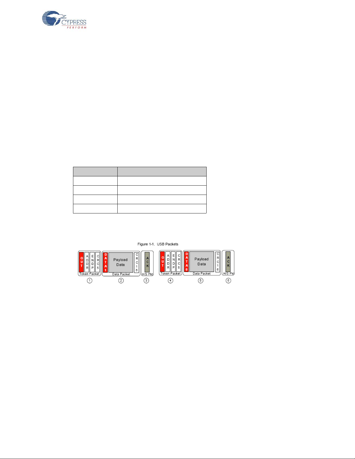
All communication over USB happen in the form of packets. Every USB packet, consist of a Packet
ID (PID). These PIDs may fall into one of the four different categories and are listed here.
PID Type PID Name
Tok e n IN , OU T, SO F, SE T UP
Data DATA0, DATA1, DATA2, MDATA
Handshake ACK, NAK, STALL, NYET
Special PRE, ERR, SPLIT, PING
Introduction to USB
The PIDs shown in bold are additions that happened in the USB 2.0 specification.
Figure 2-1. USB Packets
A regular pay load data transfer requires at least three packets: Token, Data, and Ack. Figure 2-1
illustrates a USB OUT transfer. Host traffic is shown in solid shading, while device traffic is shown
cross-hatched. Packet 1 is an OUT token, indicated by the OUT PID. The OUT token signifies that
data from the host is about to be transmitted over the bus. Packet 2 contains data, as indicated by
the DATA1 PID. Packet 3 is a hand-shake packet, sent by the device using the ACK (acknowledge)
PID to signify to the host that the device received the data error-free. Continuing with Figure 2-1, a
second transaction begins with another OUT token 4, followed by more data 5, this time using the
DATA0 PID. Finally, the device again indicates success by transmitting the ACK PID in a handshake
packet 6.
SETUP tokens are unique to CONTROL transfers. They preface eight bytes of data from which the
peripheral decodes host device requests. At full-speed, start of frame (SOF) tokens occur once per
millisecond. At high speed, each frame contains eight SOF tokens, each denoting a 125-µs
microframe.
Four handshake PIDs indicate the status of a USB transfer: ACK (Acknowledge) means 'success';
the data is received error-free. NAK (Negative Acknowledge) means 'busy, try again.' It is tempting to
assume that NAK means 'error,' but it does not; a USB device indicates an error by not responding.
FX3 Programmers Manual, Doc. # 001-64707 Rev. *C 15
Page 16

Introduction to USB
STALL means that something is wrong (probably as a result of miscommunication or lack of
cooperation between the host and device software). A device sends the STALL handshake to
indicate that it does not understand a device request, that something went wrong on the peripheral
end, or that the host tried to access a resource that was not there. It is similar to HALT, but better,
because USB provides a way to recover from a stall. NYET (Not Yet) has the same meaning as ACK
- the data was received error-free - but also indicates that the endpoint is not yet ready to receive
another OUT transfer. NYET PIDs occur only in high-speed mode. A PRE (Preamble) PID precedes
a low-speed (1.5 Mbps) USB transmission.
One notable feature of the USB 2.0 protocol is the data toggle mechanism. There are two DATA
PIDs (DATA0 and DATA1) in Figure 2-1. As mentioned previously, the ACK handshake is an
indication to the host that the peripheral received data with-out error (the CRC portion of the packet
is used to detect errors). However, the handshake packet can get garbled during transmission. To
detect this, each side (host and device) maintains a 'data toggle' bit, which is toggled between data
packet transfers. The state of this internal toggle bit is compared with the PID that arrives with the
data, either DATA0 or DATA1. When sending data, the host or device sends alternating DATA0DATA1 PIDs. By comparing the received Data PID with the state of its own internal toggle bit, the
receiver can detect a corrupted handshake packet.
The PING protocol was introduced in the USB 2.0 specification to avoid wasting bus bandwidth
under certain circumstances. When operating at full speed, every OUT transfer sends the OUT data,
even when the device is busy and cannot accept the data. Such unsuccessful repetitive bulk data
transfers resulted in significant wastage of bus bandwidth. Realizing that this could get worse at high
speed, this issue was remedied by using the new 'Ping' PID. The host first sends a short PING token
to an OUT endpoint, asking if there is room for OUT data in the peripheral device. Only when the
PING is answered by an ACK does the host send the OUT token and data.
The protocol for the interrupt, bulk, isochronous and control transfers are illustrated in the following
figures.
Figure 2-2. Two Bulk Transfers, IN and OUT
Figure 2-3. Interrupt Transfer
Figure 2-4. Isochronous Transfer
16 FX3 Programmers Manual, Doc. # 001-64707 Rev. *C
Page 17

Figure 2-5. Control Transfer
2.1.3.5 Link/Physical Layer
The link layer performs additional tasks to increase the reliability of the data transfer. This includes
byte ordering, line level framing, and so on.
More commonly known as the electrical interface of USB 2.0, this layer consists of circuits to
serialize and de-serialize data, pre and post equalization circuits and circuits to drive and detect
differential signals on the D+ and D– lines. All error handling is done at the protocol layer and there
is no discernible low level link layer to manage errors.
Introduction to USB
2.1.4 Device Detection and Enumeration
One of the most important advantages of USB over other contemporary communication system is its
plug-and-play capability. A change in termination at the USB port indicates that a USB device is
connected.
When a USB device is first connected to a USB host, the host tries to learn about the device from its
descriptors; this process is called enumeration. The host goes through the following sign on
sequence
1. The host sends a Get Descriptor-Device request to address zero (all USB devices must respond
to address zero when first attached).
2. The device responds to the request by sending ID data back to the host to identify itself.
3. The host sends a Set Address request, which assigns a unique address to the just-attached
device so it may be distinguished from the other devices connected to the bus.
4. The host sends more Get Descriptor requests, asking for additional device information. From
this, it learns every-thing else about the device such as number of endpoints, power
requirements, required bus bandwidth, and what driver to load.
All high-speed devices begin the enumeration process in full-speed mode; devices switch to
high-speed operation only after the host and device have agreed to operate at high speed. The
high-speed negotiation process occurs during USB reset, via the 'Chirp' protocol.
Because the FX2 configuration is 'soft', a single chip can take on the identities of multiple distinct
USB devices. When first plugged into USB, the FX2 enumerates automatically and downloads
firmware and USB descriptor tables over the USB cable. A soft disconnect is triggered following
which, the FX2 enumerates again, this time as a device defined by the downloaded information. This
patented two-step process, called ReNumeration™, happens instantly when the device is plugged
in, with no hint that the initial download step had occurred.
FX3 Programmers Manual, Doc. # 001-64707 Rev. *C 17
Page 18

Introduction to USB
2.1.5 Power Distribution and Management
Power management refers to the part of the USB Specification that spell out how power is allocated
to the devices connected downstream and how different communication layers operate to make best
use of the available bus power under different circumstances.
USB 2.0 supports both self and bus powered devices. Devices indicate this through their descriptors.
Devices, irrespective of their power requirements and capabilities are configured in their low power
state unless the software instructs the host to configure the device in its high power state. Low power
devices can draw up to 100 mA of current and high power devices can draw a maximum of 500 mA.
The USB host can 'suspend' a device to put it into a power-down mode. A 3 ms 'J' state (Differential
'1' indicated by D+ high D– low) on the USB bus triggers the host to issue a suspend request and
enter into a low power state. USB devices are required to enter a low power state in response to this
request.
When necessary, the device or the host issues a Resume. A Resume signal is initiated by driving a
'K' state on the USB bus, requesting that the host or device be taken out of its low power 'suspended'
mode. A USB device can only signal a resume if it has reported (through its Configuration
Descriptor) that it is 'remote wakeup capable', and only if the host has enabled remote wakeup from
that device.
This suspend-resume mechanism minimizes power consumed when activity on the USB bus is
absent
2.1.6 Device Classes
In an attempt to simplify the development of new devices, commonly used device functions were
identified and nominal drivers were developed to support these devices. The host uses the
information in the class code, subclass code, and protocol code of the device and interface
descriptors to identify if built-in drivers can be loaded to communicate with the device attached. The
human interface device (HID) class and mass storage class (MSC) are some of the commonly used
device classes.
The HID class refers to interactive devices such as mouse, keyboards, and joy sticks. This interface
use control and interrupt transfer types to transfer data because data transfer speeds are not critical.
Data is sent or received using HID reports. Either the device or the interface descriptor contains the
HID class code
The MSC class is primarily intended to transfer data to storage devices. This interface primarily uses
bulk transfer type to transfer data. At least two bulk endpoints for each direction is necessary. The
MSC class uses the SCSI transparent command set to read or write sectors of data on the disk
drive.
Details about other classes can be found at the Implementers forum website http://www.usb.org.
2.2 USB 3.0: Differences and Enhancements over USB 2.0
2.2.1 USB 3.0 Motivation
USB 3.0 is the next stage of USB technology. Its primary goal is to provide the same ease of use,
flexibility, and hot-plug functionality but at a much higher data rate. Another major goal of USB 3.0 is
power management. This is important for "Sync and Go" applications that need to trade off features
for battery life.
The USB 3.0 interface consists of a physical SuperSpeed bus in addition to the physical USB 2.0
bus. The USB 3.0 standard defines a dual simplex signaling mechanism at a rate of 5 Gbits/s.
18 FX3 Programmers Manual, Doc. # 001-64707 Rev. *C
Page 19

Introduction to USB
Inspired by the PCI Express and the OSI 7-layer architecture, the USB 3.0 protocol is also
abstracted into different layers as illustrated in the following sections.
In this document, USB 3.0 implicitly refers to the SuperSpeed portion of USB 3.0.
Figure 2-6. USB Protocol Layers
2.2.2 Protocol Layer
USB 3.0 SuperSpeed inherits the data transfer types from its predecessor retaining the model of
pipes, endpoints and packets. Nonetheless, the type of packets used and some protocols associated
with the bulk, control, isochronous, and control transfers have undergone some changes and
enhancements. These are discussed in the sections to follow.
Link Management packets are sent between links to communicate link level issues such as link
configuration and status and hence travel predominantly between the link layers of the host and the
device. For example, U2 Inactivity Timeout LMP is used to define the timeout from the U1 state to
the U2 state. The structure of a LMP is shown here.
Figure 2-7. Link Management Packet Structure
Transaction packets reproduce the functionality provided by the Token and Handshake packets and
travel between the host and endpoints in the device. They do not carry any data but form the core of
the protocol.
For example, the ACK packet is used to acknowledge a packet received. The structure of a
transaction packet is shown in Figure 2-8.
FX3 Programmers Manual, Doc. # 001-64707 Rev. *C 19
Page 20

Introduction to USB
Figure 2-8. ACK Transaction Packet
Data packets actually carry data. These are made up of two parts: a data header and the actual data.
The structure of a data packet is shown on the right.
Isochronous Time Stamp packets contain timestamps and are broadcast by the host to all active
devices. Devices use timestamps to synchronize with the host. These do not have any routing
information. The structure of an ITP is shown in Figure 2-10.
Figure 2-9. Example Data Packet
Figure 2-10. ITP Structure
OUT transfers are initiated by the host by sending a data packet on the downstream bus. The data
packet contains the device routing address and the endpoint number. If the transaction is not an
isochronous transaction, then, on receiving the data packet, the device launches an
acknowledgement packet, which also contains the next packet number in the sequence. This
process continues until all the packets are transmitted unless an endpoint responds with an error
during the transaction. In transfers are initiated by the host by sending an acknowledge packet to the
device containing the device, endpoint address and the number of packets that the host expects.
The device then starts sending the data packets to the host. The response from the host
acknowledges the previous transfer while initiating the next transfer from the device.
One important modification in the USB 3.0 specification is uni-casting in place of broadcasting.
Packets in USB 2.0 were broadcast to all devices. This necessitated every connected device to
decode the packet address to check if the packet was targeted at it. Devices had to wake up to any
USB activity regardless of its necessity in the transfer. This resulted in higher idle power. USB 3.0
packets (except ITP) are uni-casted to the target. Necessary routing information for hubs is built into
the packet.
20 FX3 Programmers Manual, Doc. # 001-64707 Rev. *C
Page 21

Introduction to USB
Another significant modification introduced in USB 3.0 relates to interrupt transfers. In USB 2.0,
Interrupt transfers were issued by the host every service interval regardless of whether or not the
device was ready for transfers. However, SuperSpeed interrupt endpoints may send an ERDY/
NRDY in return for an interrupt transfer/request from the host. If the device returned an ERDY, the
host continues to interrupt the device endpoint every service interval. If the device returned NRDY,
the host stops interrupt request or transfers to the endpoint until the device asynchronously (not
initiated by the host) notifies ERDY.
One of the biggest advantage the dual simplex bus architecture provides the USB 3.0 protocol with
is the ability to launch multiple packets in one direction without waiting for an acknowledge packet
from the other side which otherwise on a half duplex bus would cause bus contention. This ability is
exploited to form a new protocol that dictates that packets be sent with a packet number, so that any
missing or unfavorable acknowledges that comes after a long latency can be used to trigger the
retransmission of the missed packet identified by the packet number. The number of burst packets
that can be sent (without waiting for acknowledge) is communicated before the transfer.
Another notable feature of USB 3.0 is the stream protocol available for bulk transfers. Normal bulk
(OUT) transfers transfer a single stream of data to an endpoint in the device. Typically, each stream
of data is sourced from a buffer (FIFO) in the transmitter to another buffer (FIFO) in the receiver. The
stream protocol allows the transmitter to associate a stream ID (1-65536) with the current stream
transfer/request. The receiver of the stream or request sources or sinks the data to/from the
appropriate FIFO. This multiplexing of the streams achieves mimicking a pipe which can dynamically
shift its ends. Streams make it possible to realize an out-of-order execution model required for
command queuing. The concept of streams enable more powerful mass storage protocols. A typical
communication link consists of a command OUT pipe, an IN and OUT pipe (with multiple data
streams), and a status pipe. The host can queue commands, that is, issue a new command without
waiting for completion of a prior one, tagging each command with a Stream ID.
Because of the manner in which the USB 3.0 power management is defined, nonactive links (hubs,
devices) may take longer to get activated on seeing bus activity. Isochronous transfers that activate
the links take longer to reach the destination and may violate the service interval requirement. The
Isochronous-PING protocol circumvents this issue. The host sends a PING transfer before an
isochronous transaction. A PING RESPONSE indicates that all links in the path are active (or have
been activated). The host can then send or request an isochronous data packet. USB 2.0
isochronous devices can not enter low power bus state in between service intervals.
2.2.3 Link Layer
The link layer maintains link connectivity and ensures data integrity between link partners by
implementing error detection. The link layer ensure reliable data delivery by framing packet headers
at the transmitting end and detecting link level errors at the receiving end. The link layer also
implements protocols for flow control and participates in power management. The link layer provides
an interface to the protocol layer for pass through of messages between the protocol layers. Link
partners communicate using link commands.
2.2.4 Physical Layer
The two pairs of differential lines, one for OUT transfers and another for IN transfers define the
physical connection between a USB 3.0 SuperSpeed host and the device. The physical layer
accepts one byte at a time, scrambles the bits (a procedure that is known to reduce EMI emissions),
converts it to 10 bits, serializes the bits, and transmits data differentially over a pair of wires. The
clock data recovery circuit helps to recover data at the receiving end. The LFPS (Low frequency
periodic signaling) block is used for initialization and power management when the bus is IDLE.
Detection of SuperSpeed devices is done by looking at the line terminations similar to USB 2.0
devices.
FX3 Programmers Manual, Doc. # 001-64707 Rev. *C 21
Page 22

Introduction to USB
2.2.5 Power Management
USB 3.0 provides enhanced power management capabilities to address the needs of
battery-powered portable applications. Two "Idle" modes (denoted as U1 and U2) are defined in
addition to the "Suspend" mode (denoted as U3) of the USB 2.0 standard.
The U2 state provides higher power savings than U1 by allowing more analog circuitry (such as
clock generation circuits) to be quiesced. This results in a longer transition time from U2 to active
state. The Suspend state (U3) consumes the least power and again requires a longer time to wake
up the system.
The Idle modes may be entered due to inactivity on a downstream port for a programmable period of
time or may be initiated by the device, based on scheduling information received from the host. Such
information is indicated by the host to the device using the flags "Packet pending," "End of burst,"
and "Last packet." Based on these flags, the device may decide to enter an Idle mode without having
to wait for inactivity on the bus. When a link is in one of these Idle states, communication may take
place via low-frequency period signaling (LFPS), which consumes significantly lower power than
SuperSpeed signaling. In fact, the Idle mode can be exited with an LFPS transmission from either
the host or device.
The USB 3.0 standard also introduces the "Function Suspend" feature, which enables the power
management of the individual functions of a composite device. This provides the flexibility of
suspending certain functions of a composite device, while other functions remain active.
Additional power saving is achieved via a latency tolerance messaging (LTM) mechanism implemented by USB 3.0. A device may inform the host of the maximum delay it can tolerate from the time
it reports an ERDY status to the time it receives a response. The host may factor in this latency tolerance to manage system power.
Thus, power efficiency is embedded into all levels of a USB 3.0 system, including the link layer, protocol layer, and PHY. A USB 3.0 system requires more power while active. But due to its higher data
rate and various power-efficiency features, it remains active for shorter periods. A SuperSpeed data
transfer could cost up to 50 percent less power than a hi-speed transfer. This is crucial to the battery
life of mobile handset devices such as cellular phones.
2.3 Reference Documents
Some of this chapter’s contents have been sourced from the following documents:
■ Universal Serial Bus 3.0 Specification, Revision 1.0
■ Universal Serial Bus Specification, Revision 2.0
■ On-The-Go Supplement to the USB 2.0 Specification, Revision 1.3
22 FX3 Programmers Manual, Doc. # 001-64707 Rev. *C
Page 23

3. FX3 Overview
FX3 is a full-feature, general purpose integrated USB 3.0 Super-Speed controller with built-in flexible
interface (GPIF II), which is designed to interface to any processor thus enabling customers to add
USB 3.0 to any system.
The logic block diagram shows the basic block diagram of FX3. The integrated USB 3.0 Phy and
controller along with a 32-bit processor make FX3 powerful for data processing and building custom
applications. An integrated USB 2.0 OTG controller enables applications that need dual role usage
scenarios. A fully configurable, parallel, General Programmable Interface (GPIF II) provides
connection to any processor, ASIC, DSP, or FPGA. There is 512 kB of on-chip SRAM for code and
data. There are also low performance peripherals such as UART, SPI, I
to onboard peripherals such as EEPROM. The CPU manages the data transfer between the USB,
GPIF II, I2S, SPI, and UART interfaces through firmware and internal DMA interfaces.
2
C, and I2S to communicate
3.1 CPU
FX3 is powered by ARM926EJS, a 32-bit advanced processor core licensed from ARM that is
capable of executing 220 MIPS [Wikipedia] at 200 MHz, the compute power needed to perform MP3
encoding, decryption, and header processing at USB 3.0 rates for the Universal Video Class
The 'Harvard Architecture' based processor accesses instruction and data memory separate
dedicated 32-bit industry standard AHB buses. Separate instruction and data caches are built into
FX3 Programmers Manual, Doc. # 001-64707 Rev. *C 23
Page 24

FX3 Overview
ARM926EJS
Instr
TCM
(16 KB)
Data
TCM
(8 KB)
Instr
Cache
(8 KB)
Data
Cache
(8 KB)
nFIQ
nIRQ
Arm TCM
200 MHz x32-bit
1 cy accesses
Arm TCM
200 MHz x32-bit
1 cy accesses
2 x AHB
200 MHz x 32b
1,8 cy bursts
1,4,8 cy bursts
JTAG
Debug
Logic
JTAG
Signals
the core to facilitate low latency access to frequently used areas of code and data memory. In
addition, the two tightly coupled memories (TCM) (one each for data and instruction) associated with
the core provide a guaranteed low latency memory (without cache hit or miss uncertainties).
The ARM926 CPU contains a full Memory Management Unit (MMU) with virtual to physical address
translation. FX3 contains 8 KB of data and instruction caches. ARM926-EJS has 4-way set
associative caches and cache lines are 32 bytes wide. Each set therefore has 64 cache lines.
Interrupts vectored into one of the FIQ or IRQ request lines provide a method to generate interrupt
exceptions to the core.
A built-in logic provides an integrated on-chip JTAG based debug support for the processor core.
Figure 3-1. Key CPU Features
3.2 Interconnect Fabric
The Advanced Microcontroller Bus Architecture - Advanced High Performance Bus (AMBA AHB)
interconnect forms the central nervous system of FX3. This fabric allows easy integration of
processors, on-chip memories, and other peripherals using low power macro cell functions while
providing a high-bandwidth communication link between elements that are involved in majority of the
transfers. This multi-master high bandwidth interconnect has the following components:
■ AHB bus master(s) that can initiate read and write operations by providing an address and
control information. At any given instant, a bus can at most have one owner. When multiple
masters demand bus ownership, the AHB arbiter block decides the winner.
■ AHB bus slave(s) that respond to read or write operations within a given address-space range.
The bus slave signals back to the active master the success, failure, or waiting of the data
transfer. An AHB decoder is used to decode the address of each transfer and provide a select
signal for the slave that is involved in the transfer.
■ AHB bridges in the system to translate traffic of different frequency, bus width, and burst size.
These blocks are essential in linking the buses
■ AHB Slave/Master interfaces: These macro cells connect peripherals, memories, and other
elements to the bus.
24 FX3 Programmers Manual, Doc. # 001-64707 Rev. *C
Page 25

Figure 3-2. Interconnect Fabric
ARM926EJS
M
S
AHB
Bridge
AHB
Bridge
ARM AHB Bus-I
ARM AHB Bus-D
System Bus
AHB
Slave
Interface
Internal Memory
Unit (Bus Slave)
M
M M S
Peripheral-2
DMA section
(Bus Master)
Peripheral-2
Reg section
(Bus Slave)
Peripheral-1
DMA section
(Bus Master)
Peripheral-1
Reg section
(Bus Slave)
DMA bus
MMIO bus
AHB
Master
Interface
AHB
Master
Interface
AHB
Slave
Interface
AHB
Slave
Interface
AHB
Bridge
M
S
S
M
S
AHB
Bridge
The block that is attached to the
bus at this point is the master
The block that is attached to the
bus at this point is the slave
Key
M
S
AHB
Master
Interface
M
FX3 Overview
To allow implementation of an AHB system without the use of tri-state drivers and to facilitate
concurrent read/write operations, separate read and write data buses are required. The minimum
data bus width is specified as 32 bits, but the bus width can be increased for realizing higher
bandwidths.
3.3 Memory
In addition to the ARM core's tightly coupled instruction and data memories, a 512 KB general
purpose internal System memory is available in FX3. The system SRAM is implemented using 64- or
128-bit wide SRAM banks, which run at full CPU clock frequency. Each bank may be built up from
narrow SRAM instances for implementation specific reasons. A Cypress-proprietary highperformance memory controller translates a stream of AHB read and writes requests into SRAM
accesses to the SRAM memory array. This controller also manages power and clock gating for the
memory array. The memory controller is capable of achieving full 100% utilization of the SRAM array
(meaning 1 read or 1 write at full width each cycle). CPU accesses are done 64 or 128 bit at a time to
SRAM and then multiplexed/demultiplexed as 2/4 32-bit accesses on the CPU AHB bus. The
controller does not support concurrent accesses to multiple different banks in memory.
FX3 Programmers Manual, Doc. # 001-64707 Rev. *C 25
Page 26
FX3 Overview
System Bus
AHB
Slave
Interface
Memory controller for System
memory (AHB to SRAM
protocol converter +
clocking+power management)
(Bus Slave)
S
512 KB SRAM
Figure 3-3. Internal Memory Unit
The 512 KB system memory can be broadly divided into three. The first few entries of this area is
used to store DMA instructions (also known as descriptors). The DMA hardware logic executes
instructions from these locations. The last 16 K of the system memory shadows the translation table
necessary for cache operations. The remaining area can be used as user code area and/or user
data area and/or DMA buffer area.
Note 1 entry = 4 words
3.4 Interrupts
Interrupt exceptions are facilitated using the FIQ and IRQ lines of the ARM9 processor. The ISR
branch instruction for each of these interrupts is provided in the 32 byte exception table located at
the beginning of the ITCM.
The embedded PL192 vectored interrupt controller (VIC) licensed from ARM provides a hardware
based interrupt management system that handles interrupt vectoring, priority, masking and timing,
providing a real time interrupt status. The PL192 VIC supports 32 'active high' interrupt sources, the
ISR location of which can be programmed into the VIC. Each interrupt can be assigned one of the 15
programmable priority levels; equal priority interrupts are further prioritized based on the interrupt
number. While each interrupt pin has a corresponding mask and enable bits, interrupts with a
particular priority level can all be masked out at the same time if desired. Each of the '32-interrupt'
can be vectored to one of the active low FIQ or IRQ outputs of the VIC that are directly hooked to the
corresponding lines of the ARM 9 CPU. PL192 also supports daisy chained interrupts, a feature that
is not enabled in FX3.
Note Other exceptions include reset, software exception, data abort, and pre-fetch abort.
26 FX3 Programmers Manual, Doc. # 001-64707 Rev. *C
Page 27

FX3 Overview
A
H
B
L
O
G
I
C
AHB
Interface
INT_ENABLE/DISABLE[31:0]
INT_SELECT_FIQ_IRQ#[31:0]
INT_PRIORITY[4:0][0:31]
INT_PRIORITY_MASK[15:0]
INT_ADDRESS[31:0][0:31]
IRQ_STATUS[31:0]
FIQ_STATUS[31:0]
Other FIQ int lines
Masking and
Priority logic
PL 192 VIC (Simplified)
Int_line[n]
Int_endis[n]
Int_fiqirq#[n]
Int_priority[4:0][n]
Int_priority_mask
[Int_priority[4:0][n]]
CUR_INT_ADDRESS[31:0]
nFIQ
nIRQ
ARM9EJS
Core
Embedded
ICE-RT
Scan 1
Scan 2
TAP
Controller
Embedded ICE
Debug
Interface
JTAG
Interface
CPU SUBSYSTEM
(Debug logic)
FX3 (Debug logic)
JTAG to USB
Protocol Converter
(ICE box)
Real View
Debugger
PC
Figure 3-4. Vector Interrupt Controller
When both FIQ and IRQ interrupt inputs assert, the CPU jumps to the FIQ entry of the exception
table. The FIQ handler is usually placed immediately after the table, saving a branch. The FIQ mode
uses dedicated FIQ bank registers. When an IRQ line alone asserts, CPU jumps to the IRQ handler.
The IRQ handler saves the workspace on stack, reads the address of the ISR from the VIC, and
jumps to the actual ISR.
In general, high priority, low latency interrupts are vectored into FIQ while the IRQ line is reserved for
general interrupts. Re-entrant interrupts can be supported with additional firmware.
3.5 JTAG Debugger Interface
Debug support is implemented by using the ARM9EJ-S core embedded within the ARM926EJ-S
processor. The ARM9EJ-S core has hardware that eases debugging at the lowest level. The debug
extensions allow to stall the core's program execution, examine the internal state of the core and the
memory system, and further resume program execution.
Figure 3-5. ARM Debug Logic Blocks
FX3 Programmers Manual, Doc. # 001-64707 Rev. *C 27
Page 28

FX3 Overview
The ARM debugging environment has three components: A debug-host resident program (Real
View debugger), a debug communication channel (JTAG) and a target (Embedded ICE-RT). The two
JTAG-style scan chains (Scan1 and Scan2) enable debugging and 'EmbeddedICE-RT-block'
programming.
Scan Chain 1 is used to debug the ARM9EJ-S core when it has entered the debug state. The scan
chain can be used to inject instructions into ARM pipeline and also read or write core registers
without having to use the external data bus. Scan Chain 2 enables access to the EmbeddedICE
registers. The boundary scan interface includes a state machine controller called the TAP controller
that controls the action of scan chains using the JTAG serial protocol.
The ARM9EJ-S EmbeddedICE-RT logic provides integrated on-chip debug support for the
ARM9EJ-S core. The EmbeddedICE-RT logic comprises two real time watchpoint units, two
independent registers, the Debug Control Register and the Debug Status Register, and the debug
communication channel. A watchpoint unit can either be configured to monitor data accesses
(commonly called watchpoints) or monitor instruction fetches (commonly called breakpoints).
The EmbeddedICE-RT logic interacts with the external logic (logic outside the CPU subsystem)
using the debug interface. In addition, it can be programmed (for example, setting a breakpoint)
using the JTAG based TAP controller. The debug interface signals not only communicate the debug
status of the core to the external logic but also provide a means to for the external logic to raise
breakpoints if needed (disabled in FX3 by default).
ARM9EJ-S supports two debug modes: Halt mode and Monitor mode. In halt mode debug, a watchpoint or breakpoint request forces the core into debug state. The internal state of the core can then
be examined and instructions inserted into its pipeline using the TAP controller without using the
external bus thus leaving the rest of the system unaltered. The core can then be forced to resume
normal operation. Alternately, the EmbeddedICE-RT logic can be configured in monitor mode, where
watchpoints or breakpoints generate Data or Pre-fetch Aborts respectively. This enables the debug
monitor system to debug the ARM while enabling critical fast interrupt requests to be serviced.
3.6 Peripherals
3.6.1 I2S
FX3 is capable of functioning as a master mode transmitter over its Integrated Inter-chip Sound (I2S)
interface. When integrated with an audio device, the I2S bus only handles audio data, while the other
signals, such as sub-coding and control, are transferred separately.
28 FX3 Programmers Manual, Doc. # 001-64707 Rev. *C
Page 29

FX3 Overview
FX3: I2S
Master Tx
External Device:
Slave Receiver
SDA
WS
SCK
PAUSE
MUTE
DMA/SGL TRANSMIT
SGL_LEFT_DATA
SGL_RIGHT_DATA
DMA_LEFT_DATA
DMA_RIGHT_DATA
FIXED/
VAR SCK
INT_CLK
EXT_CLK
CLK_SEL
INT/EXT
STEREO/
MONO
LEFT FIRST
/RIGHT FIRST
AUDIO WIDTH
ENDIANNESS
ENABLE
Figure 3-6. I2S Blocks
The I2S block can be configured to support different audio bus widths, endianess, number of
channels, and data rate. By default, the interface is protocol standard big endian (most significant bit
first); nevertheless, the block's endianess can be reversed. FX3 also supports the left justified and
right justified variants of the protocol. When the block is enabled in left justified mode, the left
channel audio sample is sent first on the SDA line.
FX3 Programmers Manual, Doc. # 001-64707 Rev. *C 29
In the mono mode, the 'left data' is sent to both channels on the receiver (WordSelect=Left and
WordSelect=Right). Supported audio sample widths include 8, 16, 18, 24, and 32 bit. In the variable
SCK (Serial Clock) mode, WS (WordSelect) toggles every Nth edge of SCK, where N is the bus
width chosen. In fixed SCK mode, however, WS toggles every thirty-second SCK edge. In this mode,
the audio sample is zero padded to 32 bit. FX3 supports word at a time (SGL_LEFT_DATA,
SGL_RIGHT_DATA) I2S operations for small transfers and DMA based I2S operations for larger
transfers. The Serial Clock can be derived from the internal clock architecture of FX3 or supplied
from outside using a crystal oscillator. Typical frequencies for WS include 8, 16, 32, 44.1, 48, 96, and
192 KHz.
Two special modes of operation, Mute and Pause are supported. When Mute is held asserted, DMA
data is ignored and zeros are transmitted instead. When paused, DMA data flow into the block is
stopped and zeros are transmitted over the interface.
Page 30
FX3 Overview
FX3_I2C
Master
Other I2C
Master
I2C Slave1
I2C Slave2
R1 R2
VDD
SCL
SDA
3.6.2 I
2
C
Figure 3-7. I2C Block Diagram
FX3 is capable of functioning as a master transceiver and supports 100 KHz, 400 KHz, and 1 MHz
2
operation. The I
C block operates in big endian mode (Most significant bit first) and supports both
7-bit and 10-bit slave addressing. Similar to I2S, this block supports both single and burst (DMA)
data transfers.
Slow devices on its I
2
C bus can work with FX3's I2C using the clock stretching based flow control.
FX3 can function in multi-master bus environments as it is capable of carrying out negotiations with
other masters on the bus using SDA based arbitration. Additionally, FX3 supports the repeated start
feature to communicate to multiple slave devices on the bus without losing ownership of the bus in
between (see the stop last and start first feature in the following sections).
Combined format communication is supported, which allows the user to load multiple bytes of data
(including slave chip address phases) into using special registers called preamble. The user can
choose to place start (repeated) or stop bits between the bytes and can also define the master's
behavior on receiving either a NAK or ACK for bytes in the preamble. In applications such as
EEPROM reads, this greatly reduces firmware complexity and execution time by packing initial
communication bytes into a transaction header with the ability to abort the header transaction on
receiving NAK exceptions in the middle of an operation.
In addition, the preamble repeat feature available in FX3 simplifies firmware and saves time in
situations - for instance, ACK monitoring from the EEPROM to check completion of a previously
issued program operation. In this case, FX3's I
2
preamble containing the EEPROM's I
By programming the burst read count value for this block, burst reads from the slave (EEPROM for
example), can be performed with no firmware intervention. In this case, the FX3 master receiver
sends ACK response for all bytes received as long as the burst read counter does not expire. When
the last byte of the burst is received, FX3's I
C address until the device responds with an ACK.
2
C can be programmed to repeat a single byte
2
C block signals a NAK followed by a stop bit forcing the
device to stop sending data.
30 FX3 Programmers Manual, Doc. # 001-64707 Rev. *C
Page 31

3.6.3 UART
DataTerminal
Equipment(DTE)
FX3:DataCarrier
Equipment(DCE)
TX
RX
RX
TX
RTS
RTS
CTS
CTS
DMA/SGL TRANSFER
SGL_TX_DATA
SGL_RX_DATA
DMA_TX_DATA
DMA_RX_DATA
UART_ENABLE
RX_ENABLE
TX_ENABLE
LOOPBACK
RX SAMPLING
INSTANT
SW_RTS
CTS_STAT
HW_TX_FLOW_CTRL_EN
HW_RX_FLOW_CTRL_EN
# STOP BITS
PARITY ODD
PARITY STICKY
TX STICKY BIT
RX STICKY BIT
PARITY
BAUDCLK
Figure 3-8. UART Block Diagram
FX3 Overview
FX3's UART block provides standard asynchronous full-duplex transfer using the TX and RX pins.
Flow control mechanism, RTS (request to send) and CTS (clear to send) pins are supported. The
UART block can operate at numerous baud rates ranging from 300 bps to 4608 Kbps and supports
both one and two stop bits mode of operation. Similar to I2S and I
2
C blocks, this block supports both
single and burst (DMA) data transfers.
The transmitter and receiver components of the UART block can be individually enabled. When both
components are enabled and the UART set in loopback mode, the external interface is disabled;
data scheduled on the TX pin is internally looped back to the RX pin.
Both hardware and software flow control are supported. Flow control settings can individually be set
on the transmitter and receiver components. When both (Tx and Rx) flows are controlled by
hardware, the RTS and CTS signaling is completely managed by the UART block's hardware. When
the flow control is completely handled by software, software can signal a request to send using the
SW_RTS field of the block and monitor the block's CTS_STAT signal.
Transmission starts when a 0-level start bit is transmitted and ends when a 1-level stop bit is
transmitted. This represents the default 10-bit transmission mode. A ninth parity bit can be appended
to data in the 11-bit transmission mode. Both the even and odd parity variants are supported.
Optionally, a fixed check bit (sticky parity) can be inserted in place of the parity bit. The value of this
bit is configurable. Corresponding settings are also available for the Rx block.
The UART Rx line is internally oversampled by a factor of 8 and any three consecutive samples
among the eight can be chosen for the majority vote technique to decide the received bit.
Separate interface devices can be used to convert the logic level signals of the UART to and from
the external voltage signaling standards such as RS-232, RS-422, and RS-485.
FX3 Programmers Manual, Doc. # 001-64707 Rev. *C 31
Page 32

FX3 Overview
N
N-1
N-2
10
TX - SHIFT
REGISTER
RX - SHIFT
REGISTER
N
N-1
N-2
10
SHIFT REGISTER
SCLK
SSN
FX3 SPI
MASTER
SPI SLAVE
MOSI
MISO
N
N-1
N-2
10
ENDIAN
ENDIAN
ENABLE
RX_ENABLE
TX_ENABLE
LOOPBACK
ENDIAN
CONTROL
CPOL
CPHA
SSNCTRL
FW_SSN
SSN_DESELECT
SS_POL
LEAD
LAG
WID_SEL (N+1)
CLK
DMA/SGL TRANSFER
SGL_TX_DATA
SGL_RX_DATA
DMA_TX_DATA
DMA_RX_DATA
TX_BYTE_COUNT
RX_BYTE_COUNT
3.6.4 SPI
Figure 3-9. SPI Block Diagram
FX3's SPI block operates in master mode and facilitates standard full-duplex synchronous transfers
using the MOSI (Master out Slave In), MISO (Master In Slave Out), SCLK (Serial Clock), and SS
(Slave select) pins. The maximum frequency of operation is 33 MHz. Similar to the I2S and I
UART blocks, this block supports both single and burst (DMA) data transfers.
The transmit and receive blocks can be enabled independently using the TX_ENABLE/RX_ENABLE
inputs. Independent shift registers are used for the transmit and receive paths. The width of the shift
registers can be set to anywhere between 4 and 32 bits. By default, the Tx and Rx registers shift
data to the left (big endian). This can be reversed, if necessary.
The SSPOL input sets the polarity of the SSN (Slave Select) signal.The CPOL input sets the polarity
of the SCLK pin which is active high by default. The CPHA input sets the clock phases for data
transmit and capture. If CPHA is set to ‘1’, the devices agree to transmit data on the asserting edge
of the clock and capture at the de-asserting edge. However, if CPHA is set to 0, the devices agree to
2
C and
32 FX3 Programmers Manual, Doc. # 001-64707 Rev. *C
Page 33

capture data on the asserting edge of the clock and transmit at the de-asserting edge. When Idle,
the SCLK pin remains de-asserted. Hence, the first toggle of SCLK in this mode (CPHA=0) will
cause the receivers to latch data; placing a constraint on the transmitters to set up data before the
first toggle of SCLK. To SSN LEAD setting is provided to facilitate the assertion of SS (and hence the
first transmit data) a few cycles before the first SCLK toggle. The SSN LAG setting specifies the
delay in SSN de-assertion after the last SCLK toggle for the transfer. This specific mode of operation
(CPHA=0) also necessitate toggling the SSN signal between word transfers.
The SSN pin can be configured to either remain asserted always, deassert between transfers,
handled by hardware (based on CPHA configuration) or managed using software. FX3's SPI block
can share its MOSI, MISO, and SCLK pins with more than one slave connected on the bus. In this
case, the SSN signal of the block cannot be used and the slave selects need to be managed using
GPIOs.
3.6.5 GPIO/Pins
Several pins of FX3 can function as General Purpose IO s. Each of these pins is multiplexed to
support other functions / interfaces (like UART, SPI and so on). By default, pins are allocated in
larger groups to either one block or the other (Blk IO) depending on the interface mode in their
respective power domain. In a typical application, not all blocks of FX3 are used. Even so, not all
pins of blocks being used are utilized. Unused pins in each block may be overridden as a simple or
complex GPIO pin on a pin-by-pin basis.
FX3 Overview
Simple GPIO provides software controlled and observable input and output capability only. In
addition, they can also raise interrupts. Complex GPIOs add 3 timer/counter registers for each and
support a variety of time based functions. They either work off a slow or fast clock. Complex GPIOs
can also be used as general purpose timers by firmware.
There are eight complex IO pin groups, the elements of which are chosen in a modulo 8 fashion
(complex IO group 0 – GPIO 0, 8, 16., complex IO group 1- GPIO 1,9,17., and so on). Each group
can have different complex IO functions (like PWM, one shot and so on). However, only one pin from
a group can use the complex IO functions. The rest of the pins in the group are either used as block
IO or simple GPIO.
The tables below illustrate the IO Matrix in FX3.
FX3 Programmers Manual, Doc. # 001-64707 Rev. *C 33
Page 34

FX3 Overview
Table 3-1. Block IO Selection
Blk I/O
Selection
Table
Blk IO[0] GPIF IO[0] GPIF IO[0] GPIF IO[0] GPIF IO[0] GPIF IO[0] GPIF IO[0]
Blk IO[1] GPIF IO[1] GPIF IO[1] GPIF IO[1] GPIF IO[1] GPIF IO[1] GPIF IO[1]
…… … … … … …
Blk IO[29] GPIF IO[29] GPIF IO[29] GPIF IO[29] GPIF IO[29] GPIF IO[29] GPIF IO[29]
Blk IO [30] NC NC NC NC NC NC
Blk IO [31] NC NC NC NC NC NC
Blk IO [32] NC NC NC NC NC NC
Blk IO [33] GPIF IO [30] GPIF IO [30] GPIF IO [30] GPIF IO [30] GPIF IO [30] GPIF IO [30]
…… … … … … …
Blk IO[44] GPIF IO[41] GPIF IO[41] GPIF IO[41] GPIF IO[41] GPIF IO[41] GPIF IO[41]
Blk IO[45] NC NC NC NC NC NC
Blk IO[46] NC NC NC NC GPIF IO [42] UART_RTS
Blk IO[47] NC NC NC NC GPIF IO [43] UART_CTS
Blk IO[48] NC NC NC NC GPIF IO [44] UART_TX
Blk IO[49] NC NC NC NC GPIF IO [45] UART_RX
Blk IO[50] NC NC NC NC I2S_CLK I2S_CLK
Blk IO[51] NC NC NC NC I2S_SD I2S_SD
Blk IO[52] NC NC NC NC I2S_WS I2S_WS
Blk IO[53] NC UART_RTS SPI_SCK NC UART_RTS SPI_SCK
Blk IO[54] NC UART_CTS SPI_SSN I2S_CLK UART_CTS SPI_SSN
Blk IO[55] NC UART_TX SPI_MISO I2S_SD UART_TX SPI_MISO
Blk IO[56] NC UART_RX SPI_MOSI I2S_WS UART_RX SPI_MOSI
Blk IO[57] NC NC NC I2S_MCLK I2S_MCLK I2S_MCLK
Blk IO[58] I2C_SCL I2C_SCL I2C_SCL I2C_SCL I2C_SCL I2C_SCL
Blk IO[59] I2C_SDA I2C_SDA I2C_SDA I2C_SDA I2C_SDA I2C_SDA
Blk O [60] Charger det Charger det Charger det Charger det Charger det Charger det
Note: Depending on the configuration, one of the columns of the table will be selected
Choose IO
Pins from
blocks: GPIF
Choose IO
Pins from
blocks: GPIF,
UART
Choose IO
Pins from
blocks: GPIF,
SPI
Choose IO
Pins from
blocks: GPIF,
I2S
Choose IO
Pins from
blocks:
GPIF(DQ32/
extended),
UART, I2S
Choose IO
Pins from
blocks:
GPIF,UART,
SPI, I2S
Note:
(1) NC stands for Not Connected. Blk IOs 30-32,45 are Not Connected
(2) Charger detect is output only.
(3) GPIF IO are further configured into interface clock, control lines, address lines and data lines,
car-kit UART lines depending on the desired total number of GPIF pins, number of data lines and
address lines, whether the address and data lines need to be multiplexed and the car-kit mode.
Depending on the GPIF configuration selected by the user, some of the GPIF IO may remain
unconnected and may only be used as GPIOs.
34 FX3 Programmers Manual, Doc. # 001-64707 Rev. *C
Page 35

Table 3-2. Block IO override as simple/complex GPIO
FX3 Overview
FX3 Pin I/O selection
n = 0 to 60
IO Pin [0] Blk IO [0] Simple GPIO [0] Complex GPIO [0]
IO Pin [1] Blk IO [1] Simple GPIO [1] Complex GPIO [1]
…
IO Pin [8] Blk IO [8] Simple GPIO [8] Complex GPIO [0]
IO Pin [9] Blk IO [9] Simple GPIO [9] Complex GPIO [1]
…
IO Pin [59] Blk IO [59] Simple GPIO [59] Complex GPIO [3]
O Pin [60] Blk O [60] Simple GPO [60] Complex GPO [4]
Note: For each pin ‘n’ in column 1, one of column 2, 3 or 4 of the corresponding row will be selected based on the simple/override values for the corresponding pin
Override block IO as simple
GPIO [pin n] = False
Override block IO as
complex GPIO [pin n] = False
Override block IO as simple
GPIO [pin n] = True
Override block IO as
complex GPIO [pin n] = False
Override block IO as
complex GPIO [pin n] = True
Note:
(1) Pins [30-32] are used as PMODE [0-2] inputs during boot. After boot, these are available as
GPIOs.
FX3 Programmers Manual, Doc. # 001-64707 Rev. *C 35
Page 36

FX3 Overview
Table 3-3. GPIF IO block pin connection for a few configurations
Overall GPIF Pin
Count 47-pin 43-pin 35-pin 31-pin 31-pin 47-pin 43-pin 35-pin 31-pin 31-pin
Data Bus Width
32b 24b 16b 16b 8b 32b 24b 16b 16b 8b
Address Data
lines Muxed? Yes Yes Yes Yes Yes No No No No No
GPIF IO [16] CLK CLK CLK CLK CLK CLK CLK CLK CLK CLK
GPIF IO[0]
GPIF IO[1]
GPIF IO[2]
GPIF IO[3]
GPIF IO[4]
GPIF IO[5]
GPIF IO[6]
GPIF IO[7]
GPIF IO[8]
GPIF IO[9]
GPIF IO[10]
GPIF IO[11]
GPIF IO[12]
GPIF IO[13]
GPIF IO[14]
GPIF IO[15]
GPIF IO[30]
GPIF IO[31]
GPIF IO[32]
GPIF IO[33]
GPIF IO[34]
D0/
A0
D1/ A1D1 /
D2/
A2
D3/
A3
D4/
A4
D5/
A5
D6/
A6
D7/
A7
D8/
A8
D9/
A9
D10/
A10
D11/
A11
D12/
A12
D13/
A13
D14/
A14
D15/
A15
D16/
A16
D17/
A17
D18/
A18
D19/
A19
D20/
A20
D0/
A0
A1
D2/
A2
D3/
A3
D4/
A4
D5/
A5
D6/
A6
D7/
A7
D8/
A8
D9/
A9
D10/
A10
D11/
A11
D12/
A12
D13/
A13
D14/
A14
D15/
A15
D16/
A16
D17/
A17
D18/
A18
D19/
A19
D20/
A20
D0/
A0
D1/
A1
D2/
A2
D3/
A3
D4/
A4
D5/
A5
D6/
A6
D7/
A7
D8/
A8
D9/
A9
D10/
A10
D11/
A11
D12/
A12
D13/
A13
D14/
A14
D15/
A15
D0/
A0
D1/
A1
D2/
A2
D3/
A3
D4/
A4
D5/
A5
D6/
A6
D7/
A7
D8/
A8
D9/
A9
D10/
A10
D11/
A11
D12/
A12
D13/
A13 C15
D14/
A14 C14
D15/
A15 C13
D0/
A0
D1/
A1
D2/
A2
D3/
A3
D4/
A4
D5/
A5
D6/
A6
D7/
A7
D0 D0 D0 D0 D0
D1 D1 D1 D1 D1
D2 D2 D2 D2 D2
D3 D3 D3 D3 D3
D4 D4 D4 D4 D4
D5 D5 D5 D5 D5
D6 D6 D6 D6 D6
D7 D7 D7 D7 D7
D8 D8 D8 D8 A0
D9 D9 D9 D9 A1
D10 D10 D10 D10 A2
D11 D11 D11 D11 A3
D12 D12 D12 D12 A4
D13 D13 D13 D13 A5
D14 D14 D14 D14 A6
D15 D15 D15 D15 A7
D16 D16
D17 D17
D18 D18
D19 D19
D20 D20
36 FX3 Programmers Manual, Doc. # 001-64707 Rev. *C
Page 37

FX3 Overview
D21/
GPIF IO[35]
A21
D22/
GPIF IO[36]
A22
D23/
GPIF IO[37]
A23
D24/
GPIF IO[38]
A24 n/u
D25/
GPIF IO[39]
A25 C15
D26/
GPIF IO[40]
A26 C14
D27/
GPIF IO[41]
A27 C13
D28/
GPIF IO[42]
A28
D29/
GPIF IO[43]
A29 C15
D30/
GPIF IO[44]
A30 C14
D31/
GPIF IO[45]
A31 C13
GPIF IO[29] C12 C12 C12 C12 C12 C12/
GPIF IO[28] C11 C11 C11 C11 C11 C11/
GPIF IO[27] C10 C10 C10 C10 C10 C10/
D21/
A21
D22/
A22
D23/
A23
D21 D21
D22 D22
D23 D23
D24 A0
D25 C15/
A1
D26 C14/
A2
D27 C13/
A3
D28 A0
D29 C15/
A1
D30 C14/
A2
D31 C13/
A3
A0
A1
A2
C12/
A4
C11/
A5
C10/
A6
C12/
A4
C11/
A5
C10/
A6
C12/
A0
C11/
A1
C10/
A2
GPIF IO[26] C9 C9 C9 C9 C9 C9/ A3 C9/ A7 C9/ A7 C9/ A3 C9/
GPIF IO[25] C8 C8 C8 C8 C8 C8/ A4 C8/ A8 C8/ A8 C8/ A4 C8/
GPIF IO[24] C7 C7 C7 C7 C7 C7/ A5 C7/ A9 C7/ A9 C7/ A5 C7/
GPIF IO[23] C6 C6 C6 C6 C6 C6/ A6 C6/
A10
GPIF IO[22] C5 C5 C5 C5 C5 C5/ A7 C5/
A11
C6/
A10
C5/
A11
C6/ A6 C6/
C5/ A7 C5/
C4 C4 C4 C4 C4 C4 C4 C4 C4 C4
GPIF IO[21]
C3 C3 C3 C3 C3 C3 C3 C3 C3 C3
GPIF IO[20]
C2 C2 C2 C2 C2 C2 C2 C2 C2 C2
GPIF IO[19]
C1 C1 C1 C1 C1 C1 C1 C1 C1 C1
GPIF IO[18]
C0 C0 C0 C0 C0 C0 C0 C0 C0 C0
GPIF IO[17]
Note:
(1) Depending on the configuration, one of the columns of the table will be selected
(2) Empty cells imply no connection
(3) Cx - Control line # x
(4) Ay - Address line #y
(5) Dz - Data line #z
C12/
A8
C11/
A9
C10/
A10
A11
A12
A13
A14
A15
FX3 Programmers Manual, Doc. # 001-64707 Rev. *C 37
Page 38

FX3 Overview
GPIF II
STATE
MACH.
(256 states)
λ
ω
σ
Lamda
(32)
Omega
(8)
Sigma
(33)
Certain pins, like the USB lines have specific electrical characteristics and are connected directly to
the USB IO-System. They do not have GPIO capability.
Pins belonging to the same block share the same group setting (say alpha) for drive strengths. Pins
of a block overridden as GPIO share the same group setting (say beta) for their drive strength. FX3
provides software controlled pull up (50 kΏ) or pull down (10 kΏ) resistors internally on all digital I/O
pins.
3.6.6 GPIF
The FX3 device includes a GPIF II interface that provides an easy and glue less interface to popular
interfaces such as asynchronous SRAM, synchronous SRAM, Address Data Multiplexed interface,
parallel ATA, and so on. The interface supports up to 100 MHz. and has 40 programmable pins that
are programmed by GPIF Waveform Descriptor as data, address, control, or GPIO function. For
example, the GPIF II can be configured to a 16-bit ADM (Address/Data Multiplex), seven control
signals, and seven GPIO
The GPIF II interface features the following:
■ The ability to play both the master and slave role, eliminating the need for a separate slave FIFO
interface.
■ A large state space (256 states) to enable more complex pipelined signaling protocols.
■ A wider data path supporting 32-bit mode in addition to 16- and 8-bit.
■ A deeper pipeline designed for substantially higher speed (more than 200 MHz internal clock
frequency - “Edge Placement Frequency")
■ High frequency I/Os with DLL timing correction (shared with other interface modes), enabling
interface frequencies of up to 100 MHz.
■ 40 programmable pins
The heart of the GPIF II interface is a programmable state machine.
Figure 3-10. State Machine
This state machine
■ Supports up to 256 different states
■ Monitors up to 32 input signals (lamda) to transition between states
■ Provides for transition to two different states from the current state
■ Can drive/control up to eight external pins of the device (omega)
■ Can generate up to 33 different internal control signals (sigma)
The GPIF II is not connected directly to the USB endpoint buffers. Instead it is connected to FX3's
internal DMA network. This enables the FX3's high-performance CPU to have more control over and
access to the data flows in the application thus enabling a wider range of applications, including
ones that process, rather than just route, the actual data flows.
38 FX3 Programmers Manual, Doc. # 001-64707 Rev. *C
Page 39

3.7 DMA Mechanism
CPU
PERIPHERAL 1
PERIPHERAL 2
SYSTEM
MEMORY
1
2
3
FX3
4
CPU
PERIPHERAL 1
PERIPHERAL 2
SYSTEM
MEMORY
1
2
FX3
4
3
CPU
PERIPHERAL 1
PERIPHERAL 2
SYSTEM
MEMORY
FX3
BRIDGE
SYSTEM AHB
DMA AHB
PERIPHERAL 1_AHB
PERIPHERAL_2_AHB
Figure 3-11. DMA Mechanism
Non-CPU intervened data chunk transfers between a peripheral and CPU or system memory,
between two different peripherals or between two different gateways of the same peripheral, loop
back between USB end points, are collectively referred to as DMA in FX3.
Figure 3-11 shows a logical paths of data flow; however, in practice, all DMA data flows through the
System memory as shown in the following figure.
FX3 Overview
Figure 3-12. System Memory
FX3 Programmers Manual, Doc. # 001-64707 Rev. *C 39
Page 40

FX3 Overview
PERIPHERAL_AHB
TH0
TH1
TH2
TH3
SCK0
SCK1
SCK2
SCK32
THR_SCK_MAP
settings (FW or fixed)
Peripheral Core
Thread controllerDMA Adapter
DATA
ADDR
PERIPHERAL_N
L
O
G
I
C
FX3
External
Host or
device
As explained earlier, the CPU accesses the System Memory (Sysmem) using the System AHB and
the DMA paths of the peripherals are all hooked up to the DMA AHB. Bridge(s) between the System
bus and the DMA bus are essential in routing the DMA traffic through the Sysmem.
The following figure illustrates a typical arrangement of the major DMA components of any DMA
capable peripheral of FX3.
Figure 3-13. DMA Components
The figure shows a partition of any FX3 peripheral from a DMA view point. Any FX3 peripheral can
be split into three main components - DMA adapter, thread controller, and peripheral core. The
peripheral attaches to the DMA fabric using AHB, width of which determines the throughput of the
peripheral. The peripheral core implements the actual logic of the peripheral (I
2
C, GPIF, and USB).
Data transfers between the peripheral core and the external world is shown to happen over two
buses - address and data. These buses symbolize that the peripherals of FX3 do not present
themselves as a single large source or sink for data; rather the external host (or device) gets to index
the data to/from different addresses.
In practice though, physical address and data buses may not exist for all peripherals. Each
peripheral has its own interface to communicate addresses and data. For example, all information
exchanges in the USB block happen over the D+ and D– lines. The core logic extracts the address
from the token packet and data from the data packet. The I
2
C interface exchanges all information
over the SDA lines synchronized to a clock on the SCL line. The GPIF interface on the other hand
can be configured to interface using a separate physical address and data bus.
The address specified by the external host (or device) is used to index data from/into one of the
many entities called 'Sockets' which logically present themselves, at the interface, as a chain of
buffers. The buffer chains themselves can be constructed in one of a several possible ways
depending on the application.
40 FX3 Programmers Manual, Doc. # 001-64707 Rev. *C
Page 41

FX3 Overview
(C) multiple buffers of
different sizes
chained to create
a large buffer
(B) multiple buffers of
the same size
chained to create
a large buffer
(A) a single large
buffer of fixed size
(D) a single large
circular buffer
(E) circular buffer
using multiple
sub buffers
Figure 3-14. .DMA Configurations
The buffers do not reside in the peripherals; they are created (memory allocated) in the Sysmem
area and a pointer is made available to the associated socket. Therefore any DMA access to the
Sysmem needs to go through the DMA and the System AHB, the widths of which directly determine
the DMA bandwidth.
Certain peripherals may contain tens of sockets, each associated with different buffer chains. To
achieve reasonably high bandwidth on DMA transfers over sockets while maintaining reasonable
AHB bus width, Socket requests for buffer reads/ writes are not directly time multiplexed; rather the
sockets are grouped into threads, the requests of which are time multiplexed. Only one socket in a
group can actively execute at any instant of time. The thread handling the socket group needs to be
reconfigured every time a different socket in the group needs to execute. The thread-socket relations
are handled by the thread controller. The DMA adapter block converts read/write queries on the
threads to AHB requests and launches them on to the AHB. A single thread controller and DMA
adapter block may be shared by more than one peripheral.
A socket of a peripheral can be configured to either write to or read from buffers, not both. As a
convention, sockets used to write into system buffers are called 'Producers' and the direction of data
flow in this case is referred to as 'Ingress'. Conversely, sockets used to read out system buffers are
called 'Consumers' and the direction of data flow in this case is referred to as 'Egress'. Every socket
has a set of registers, which indicate the status of the socket such as number of bytes transferred
over the socket, current sub buffer being filled or emptied, location of the current buffer in memory,
and no buffer available.
A DMA transfer in FX3 can be envisioned as a flow of data from a producer socket on one peripheral
to a consumer socket on the other through buffers in the Sysmem. Specific DMA instructions called
'Descriptors' enable synchronizing between the sockets. Every buffer created in the Sysmem has a
descriptor associated with it that contains essential buffer information such as its address, empty/full
status and the next buffer/descriptor in chain. Descriptors are placed at specific locations in the
Sysmem which are regularly monitored and updated by the peripherals' sockets.
In a typical DMA transaction, the data source-peripheral sends data over the producing socket,
which fills the current buffer of the latter. Upon the last byte of the producer's current buffer being
written, the producer socket updates the descriptor of its current buffer and loads the next buffer in
chain. This process goes on until either the buffer chain ends or the next buffer in chain is not free
(empty to produce into). The corresponding consumer socket waits until the buffer it points to
becomes available (gets filled to consume from). When available, the data destination-peripheral is
notified to start reading the buffer over the consumer socket. When the last byte of the current buffer
is read, the consumer socket updates the descriptor of its current buffer and loads the next buffer in
FX3 Programmers Manual, Doc. # 001-64707 Rev. *C 41
Page 42

FX3 Overview
00000000
Reserved
Boot ROM
MMIO Space IP_ FFF
DTCM
Reserved
Main System
SRAM
3FFFFFFF
40000000
7FFFFFFF
80000000
DFFFFFFF
E0000000
EFFFFFFF
E 0000000
E000 FFFF
IP_ 003
IP_ 002
IP_001
CPU Vectors
ISR Code,
RTOS Kernel
etc.
E 0010000
E 001 FFFF
E 0020000
E002 FFFF
EFFF0000
EFFFFFFF
00000020
RESET (N/ A)
FFFFFFFF
F0000000
UNDEF INSTR
SW INT
ABORT ( PREF)
ABORT ( DATA)
RESERVED
IRQ
FIQ
00000000
00000004
00000008
0000000C
00000010
00000014
00000018
0000001C
‘Regular’
MMIO Space
E0007FFF
E 0008000
E 0000000
E000FFFF
SCK_ GBL
SCK_00
E 000FF 00
E 000807f
SCK_DSCR E 0008000
E000807C
EVENT
RESERVED
SCK_ SIZE
SCK_ COUNT
SCK_ STATUS
DSCR_ BUFFER
DSCR_ SYNC
DSCR_ CHAIN
DSCR_ SIZE
E0008004
E0008008
E000800C
E0008020
E0008024
E0008028
E000802C
SCK_ INTR0
TIMEOUT_ ON0
TIMEOUT_ CTR
TIMEOUT_ ST0
TIMEOUT_ EN0
E000 FF00
E000 FF20
E000 FF40
E000 FF60
E000 FF80
SCK_ FD
E000FE80
E 000FEFF
ITCM
BFFFFFFF
C0000000
Reserved
0FFFFFFF
10000000
1FFFFFFF
20000000
ARM PL 192 VIC
FFFFF000
FFFFFFFF
Unused
Unused
( variable)
ISR Data
RTOS Tables
etc.
10000000
00000000
( variable)
DMA Descriptors
Translation Table
( all sections)
MAX-16 KB
MAX
40000000
Code, Data ,
DMA Buffers
40000000+16 *#dscr-1
40000000+16 *#dscr
Unused
Unused
Peripheral Config
Peripheral logic
Specific reg
#1
#N
E 0000000
E0007 FFF
Unused
Peripheral logic
Specific reg
Peripheral ID,Power
The proc port and the USB port peripherals
have a dedicated 64KB MMIO region, 32 KB
of which is alloted for sockets. The I2S, I2C,
UART and SPI each have a dedicated 4KB
register space but share the 32 KB socket
area……………………………………… …..
CPU comes out of reset with TCM’s
disabled and VINITHI=1. Reset will
jump to FFFF0000 directly into
BootROM. BootROM enabled TCMs
and moves vectors to 00000000
Some memories (SysMem, BootROM) fill entire address
space alloted, regardless of their physical size. If physical
memory is smaller, most significant address bits are
ignored (memory ‘repeats’). This is not to be used, and
usually fault protected by the MMU ……………………..
chain. This process goes on until either the buffer chain ends or the next buffer in chain is not
available. The producer and consumer socket only share the buffer/descriptor chain. It is not
necessary for them to be executing the same descriptor in the chain at any given instant.
In nonconventional DMA transactions, the producer and consumer sockets can be two different
sockets on the same peripheral. In some cases (for example, reading F/W over I
destination peripheral or consumer socket. In this case, CPU is assumed to be the consumer.
Conversely, CPU can act as a producer to a consumer socket on the destination peripheral (for
example, printing debug messages over UART).
3.8 Memory Map and Registers
Figure 3-15. Memory Map
2
C), there is no
42 FX3 Programmers Manual, Doc. # 001-64707 Rev. *C
The ARM PL192 VIC is located outside the regular MMIO space, on top of the BootROM at location
FFFFF000. This is conform the PL192 TRM, to facilitate single instruction jump to ISR from the
vector table at location 00000000 for IRQ and FIQ. For more details see ARM PL192 TRM.
A peripheral of FX3 typically contains the following registers
■ ID register
■ Clock, power config register
■ Peripheral specific config registers
■ Interrupt enable, mask an status registers
■ Error registers
■ Socket registers for sockets associated with the peripheral
Page 43

3.9 Reset, Booting, and Renum
WB Benicia
Boot
Loader
ROM
USB
Processor
AP
I2C
Legacy
PMMC
Or
Async
SRAM
Or
Async
ADMux
Or
Sync
ADMux
USB Host
(PC)
EEPROM
EFUSE
PMODE[2:0]
Resets in FX3 are classified into two - hard reset and soft reset.
A power on reset (POR) or a Reset# pin assertion initiates a hard reset. Soft Reset, on the other
hand, involves the setting the appropriate bits in the certain control registers.
Soft Resets are of two types - CPU Reset and Device Reset
CPU reset involves resetting the CPU Program Counter. Firmware does not need to be reloaded
following a CPU Reset. Whole Device Reset is identical to Hard Reset. The firmware must be
reloaded following a Whole Device Reset.
Figure 3-16. Reset
FX3 Overview
FX3's flexible firmware loading mechanism allows code to be loaded from a device connected on the
2
I
C bus (an EEPROM for example) or from a PC acting as a USB host or from an application
processor (AP) connected on the flexible GPIF.
A hard reset forces FX3 to execute its built in boot-loader code which first checks for the boot
information bits programmed in the eFuse. The boot information bits are meant primarily to indicate
the source of FX3's firmware (also known as boot mode). If this information is not available in the
eFuse, the state of the PMODE pins is scanned to determine the boot mode and enable the
appropriate interface block (GPIF, I
For example, the code may reside in the EEPROM attached to FX3's I
2
C, or USB).
2
C bus. In some cases, an
intelligent processor connected to the GPIF of FX3 may also be used to download the firmware for
FX3. The processor can write the firmware bytes using the Sync ADMux, Async ADMux, or the
Async SRAM protocol. In addition, the AP can also use the MMC initialization and write commands
(PMMC legacy) to download firmware over its interface with FX3.
Alternately, the user may simply wish to download the code from a PC using a USB cable. When
FX3 is configured for USB boot, the boot loader first enables FX3's USB block to accept vendor
commands over a bulk end point. When plugged into the host, the device enumerates with a
Cypress default VID and PID. The actual firmware is then downloaded using Cypress drivers. If
required, the firmware can then reconfigure the USB block (such as change the IDs and enable
more end points) and simulate a disconnect-event (soft disconnect) of the FX3 device from the USB
bus. On soft reconnect, FX3 enumerates with the new USB configuration. This two step patented
process is called renumeration.
FX3 Programmers Manual, Doc. # 001-64707 Rev. *C 43
Page 44

FX3 Overview
%
CLKIN CLKOUT
PLL_SYS_CLK_16
PLL_SYS_CLK_4
PLL_SYS_CLK_2
PLL_SYS_CLK_1
DIVIDE
PERIPHERAL_CLK
4:1
MUX
CLOCK SELECT AND DIVIDE BLOCK
PLL_SYS_
CLKS[3:0]
PLL_SYS_
CLK_SEL
SEL_CLK
_DIV[N:0]
DIV_CLK
_OUT
CSD
The boot loader is also responsible for restoring the state of FX3 when the device transitions back
from a low power mode to the normal active power mode. The process of system restoration is
called 'Warm boot'.
3.10 Clocking
Clocks in FX3 are generated from a single 19.2 MHz (±100 ppm) crystal oscillator. It is used as the
source clock for the PLL, which generates a master clock at frequencies up to up to 500 MHz. Four
system clocks are obtained by dividing the master clock by 1, 2, 4, and 16. The system clocks are
then used to generate clocks for most peripherals in the device through respective clock select and
divide (CSD) block A CSD block is used to select one of the four system clocks and then divide it
using the specified divider value. The depth and accuracy of the divider is different for different
peripherals,
Figure 3-17. CSD
The CPU clock is derived by selecting and dividing one of the four system clocks by an integer factor
anywhere between 1 and 16. The bus clocks are derived from the CPU clock. Independent 4-bit
dividers are provided for both the DMA and MMIO bus clocks. The frequency of the MMIO clock,
however, must be an integer divide of the DMA clock frequency.
A 32 kHz external clock source is used for low-power operation during standby. In the absence of a
32 kHz input clock source, the application can derive this from the reference clock produced by the
oscillator.
Certain peripherals deviate from the general clock derivation strategy. The fast clock source of GPIO
is derived from the system clocks using a CSD. The core clock is a fixed division of the fast clock.
The slow clock source of GPIO is obtained directly from the reference clock using a programmable
divider. The standby clock is used to implement 'Wake-Up' on GPIO. The I2S block can be run off an
internal clock derived from the system clocks or from an external clock sourced through the
I2S_MCLK pin of the device.
Exceptions to the general clock derivation strategy are blocks that contain their own PLL, because
they include a PHY that provides its clock reference. For example, the UIB block derives its
'epm_clk', 'sie_clk', 'pclk', and 'hd3_clk' using the standby clock, dma-bus clock, 30/120 MHz clock
from the USB2 PHY and a 125 MHz clock from the USB3PHY. The sie_clk runs the USB 2.0 logic
blocks while USB 3.0 logic blocks are run using the pclk. The hd3_clk runs certain host and USB 3.0
logic blocks while the epm_clk runs the end point manager.
44 FX3 Programmers Manual, Doc. # 001-64707 Rev. *C
Page 45

Figure 3-18. Clock Generation Structure
CLKIN
MULTIPLY
DIVIDE
CLKOUT_1
CLKOUT_2
CLKOUT_4
CLKOUT_16
SYS_PLL
PLL_SYS_
CLKS[3:0]
PLL_SYS_
CLK_SEL
SEL_CLK
_DIV[N:0]
DIV_CLK
_OUT
CSD
PLL_SYS_
CLKS[3:0]
PLL_SYS_
CLK_SEL
SEL_CLK
_DIV[N:0]
DIV_CLK
_OUT
CSD
CLKIN
SEL_CLK
_DIV[N:0]
DIV_CLK
_OUT
%
PLL_SYS_
CLKS[3:0]
PLL_SYS_
CLK_SEL
SEL_CLK
_DIV[N:0]
DIV_CLK
_OUT
CSD
CLKIN
SEL_CLK
_DIV[N:0]
DIV_CLK
_OUT
%
CLKIN
SEL_CLK
_DIV[N:0]
DIV_CLK
_OUT
%
CLKIN
SEL_CLK
_DIV[N:0]
DIV_CLK
_OUT
%
CLKIN
SEL_CLK
_DIV[N:0]
DIV_CLK
_OUT
%
Xtal
Osc
CLKIN
SEL_CLK
_DIV[N:0]
DIV_CLK
_OUT
%
USB2PHY
PLL
CLKIN
CLKOUT_480
CLKOUT_30
USB3PHY
PLL
CLKIN
CLKOUT_125
CLKOUT_5G
CLKIN
DIV_CLK
_OUT
% 4
CLKIN
DIV_CLK
_OUT
% 4
UIB CLK
MUX
uib_epm_clk
uib_hd3_clk
uib_sie_clk
uib_p_clk
reference clock
peripheral_core_clk
i2s_core_clk
gpio_fast_clk
gpio_core_clk
gpio_slow_clk
gpio_standby_clk
cpu_core_clk
mmio_bus_clk
dma_bus_clk
dma_bus_clk_i
standby_clk_i
usb2_clk120_i
usb2_clk30_i
usb3_clk125_i
Clk_32_in
Crystal_in
Crystal_out
PLL_CFG.DIV
PLL_CFG.MUL
mclk_i2s_in
FX3_PERIPH_CLK_CFG.
SYSCLK_SEL
FX3_I2S_CLK_CFG.
SELCLK_DIV
FX3_I2S_CLK_CFG.
SYSCLK_SEL
FX3_I2S_CLK_CFG.
SEL_M_CLK
FX3_GPIO_FCLK_CFG.
SYSCLK_SEL
FX3_GPIO_FCLK_CFG.
SELCLK_DIV
PLL_SYS_CLK_SEL
FX3_GPIO_SCLK_CFG.
SELCLK_DIV
FX3_GPIO_CLK_CFG.
SELCLK_DIV
FX3_STANDBY_CLK_CFG.
SELCLK_DIV
FX3_CPU_CLK_CFG.
SELCLK_DIV
FX3_CPU_CLK_CFG.
SYSCLK_SEL
FX3_MMIO_CLK_CFG.
SELCLK_DIV
FX3_DMA_CLK_CFG.
SELCLK_DIV
STANDBY_
CLK_SEL
UIB CLOCK
SRCS.CFG
Note…………………………………………………….
UART baud rate is 1/8
th
of uart_core_clk…………..
I2C operating frequency is 1/10
th
of I2C core clock
SPI operating frequency is ½ of spi core clock…….
CLKIN
DIV_CLK
_OUT
% 4
FX3 Overview
The CPU, DMA, and MMIO clock domains are synchronous to each other. However, every
peripheral assumes its core clock to be fully asynchronous from other peripheral core clocks, the
computing clock or the wakeup clock.
If the core (peripheral) clock is faster than the bus clock, the DMA adapter for the block runs in the
core clock domain. The DMA adapter takes care of the clock crossing on it's interconnect side. If the
core clock is slower than the bus clock, the DMA adapter for that block runs in the bus clock domain.
The DMA adapter takes care of the clock crossing on its core IP side.
FX3 Programmers Manual, Doc. # 001-64707 Rev. *C 45
Page 46

FX3 Overview
Core Logic
Block XYZ
I/ O
Pads
DMA / B us
Adapter
Wake Up
Logic
I/O
Matrix
System
Interconnects
Block XYZ
Clock Domain
Always - On
Clock / Power / Re set Domain
Processor / Bus
Clock Domain
wakeup
Block XYZ Power Domain
Core Logic
Block XYZ
I/ O
Pads
DMA / Bus
Adapter
Wake Up
Logic
I/O
Matrix
System
Interconnects
Block
XYZ
Clock
Domain
Always - On
Clock / Power / Reset Domain
Processor / Bus
Clock Domain
wakeup
Block XYZ Power Domain
(a) Core Clock >Bus clock
(b) Bus clock>Core Clock
Figure 3-19. DMA Adaptor
3.11 Power
3.11.1 Power Domains
Power supply domains in FX3 can be mainly classified in four - Core power domain, Memory power
domain, IO power domain, and Always On power domain
Core power domain encompasses a large section of the device including the CPU, peripheral logic,
and the interconnect fabric. The system SRAM memory resides in the Memory power domain. IO
logic dwell in their respective peripheral IO power domain (either of the I
I2S-UART IO -SPI IO-GPIO power domain, Clock IO power domain, USB IO power domain, and
Processor Port IO power domain). The Always On power domain hosts the power management
controller, different wake-up sources and their associated logic.
2
C IO power domain,
3.11.2 Power Management
Wake-up sources forces a system in suspend or standby state to switch to the normal power
operation mode. These are distributed across peripherals and configured in the 'Always On global
configuration block'. Some of them include level match on level sensitive wakeup IOs, toggle on
edge sensitive wake-up IOs, activity on the USB 2.0 data lines, OTG ID change, LFPS detection on
USB 3.0 RX lines, USB connect event, and watchdog timer - timeout event.
The 'Always On global configuration block' runs off the standby clock and will be turned off only in
the lowest power state (core power down).
At any instant, FX3 is in one of the four power modes - normal, suspend, standby, or core power
down. In a typical scenario, when FX3 is actively executing its tasks, the system is in normal mode.
The usual clock gating techniques in peripherals minimize the overall power consumption.
On detecting prolonged periods of inactivity, the chip can be forced to enter the suspend mode. All
ongoing port (peripheral) activities are wrapped up, ports disabled, and wake up sources are set
before entering the suspend state. In applications involving USB 3.0, the USB3 PHY is forced into
the U3 state. USB2PHY, if used, is forced into suspend. The System RAM transitions to a low power
stand by state; read and write to RAM cannot be performed. The CPU is forced into the halt state.
The ARM core will retain its state, including the Program Counter inside the CPU. All clocks except
the 32-KHz standby are turned off by disabling the System PLL is through the global configuration
block. In the absence of clocks, the IO pins can be frozen to retain their state as long as the IO
power domain is not turned off The INT# pin can be configured to indicate FX3's presence in low
power mode.
Further reduction in power is achieved by forcing FX3 into stand-by state where, in addition to
disabling clocks, the core power domain is turned off. As in the case of suspend, IO states of
powered peripheral IO domains are frozen and ports disabled. Essential configuration registers of
46 FX3 Programmers Manual, Doc. # 001-64707 Rev. *C
Page 47

FX3 Overview
logic blocks are first saved to the System RAM. Following this, the System RAM itself is forced into
low power memory retention only mode. Warm boot setting is enabled in the global configuration
block. Finally the core is powered down. When FX3 comes out of standby, the CPU goes through a
reset; the boot-loader senses the warm boot mode and restores the system to its original state after
loading back the configuration values (including the firmware resume point) from the System RAM.
Optionally, FX3 could be powered down from its Standby mode (core power down). This involves an
additional process of removing power from the VDD pins. Contents of System SRAM are lost and IO
pins go undefined. When power is re-applied to the VDD pins, FX3 will go through the normal power
on reset sequence.
FX3 Programmers Manual, Doc. # 001-64707 Rev. *C 47
Page 48

FX3 Overview
48 FX3 Programmers Manual, Doc. # 001-64707 Rev. *C
Page 49

4. FX3 Software
Master/Slave
Peripheral
User
Implementation
FX3
- User application
- Application framework
- FX3 APIs
- Low level drivers
- RTOS
USB Host
(SS/HS/FS)
- User application
- Cypress generic USB driver
- USB 3.0 Bus/Hub driver
- USB xHCI driver
USB Device
(HS/FS/LS)
User Device
Implementation
P-PortI2C/I2S/
UART/SPI
U-Port
USB HS/FS/LS
USB SS/HS/FS
GPIF II
Cypress provided software
User or customer software
Third-party or platform software
Cypress EZ-USB FX3 is the next generation USB 3.0 peripheral controller. This is a highly integrated
and flexible chip which enables system designers to add USB 3.0 capability to any system. The FX3
comes with the easy-to-use EZ-USB tools providing a complete solution for fast application
development.
Cypress EZ-USB FX3 is a user programmable device and is delivered with a complete software
development kit.
4.1 System Overview
Figure 4-1illustrates the programmer's view of FX3. The main programmable block is the FX3
device. The FX3 device can be set up to
■ Configure and manage USB functionality such as charger detection, USB device/host detection,
and endpoint configuration
■ Interface to different master/slave peripherals on the GPIF interface
■ Connect to serial peripherals (UART/SPI/GPIO/I
■ Set up, control, and monitor data flows between the peripherals (USB, GPIF, and serial
peripherals)
■ Perform necessary operations such as data inspection, data modification, header/footer
information addition/deletion
2
C/I2S)
Figure 4-1. Programming View of FX3
FX3 Programmers Manual, Doc. # 001-64707 Rev. *C 49
Page 50

FX3 Software
FX3 Development Tools
Integrated C/C++
Development Environment
Debugger
JTAG
Compiler
Assembler
Linker
GPIF II Designer
FX3 Firmware Stack
FX3 Firmware Examples
Customer Firmware
FX3 Firmware Framework
FX3 API Library
RTOS
FX3 Host Software
(Windows PC)
Cypress Generic
USB Driver
C++/C# APIs
Cy Control Center/
Bulkloop/ Streamer
Windows USB DI
Customer Software
Cypress provided Software
Third Party Software
The two other important entities that are external to the FX3 are
■ USB host/device
❐ When the FX3 is connected to a USB host, it functions as a USB device. The FX3 enumerates
as a super-speed, high-speed, or full-speed USB peripheral corresponding to the host type.
❐ When a USB device is connected, the FX3 plays the role of the corresponding high-speed,
full-speed or low-speed USB host.
■ GPIF II master/slave: GPIF II is a fully configurable interface and can realize any application
specific protocol as described in GPIF™ II Designer on page 191. Any processor, ASIC, DSP, or
FPGA can be interfaced to the FX3. FX3 bootloader or firmware configures GPIF II to support the
corresponding interface.
4.2 FX3 Software Development Kit (SDK)
The FX3 comes with a complete software development solution as illustrated in the following figure.
Figure 4-2. FX3 SDK Components
4.3 FX3 Firmware Stack
Powerful and flexible applications can be rapidly built using FX3 firmware framework and FX3 API
libraries.
4.3.1 Firmware Framework
The firmware (or application) framework has all the startup and initialization code. It also contains
the individual drivers for the USB, GPIF, and serial interface blocks. The framework
■ Defines the program entry point
4.3.2 Firmware API Library
50 FX3 Programmers Manual, Doc. # 001-64707 Rev. *C
■ Performs the stack setup
■ Performs kernel initialization
■ Provides placeholders for application thread startup code
The FX3 API library provides a comprehensive set of APIs to control and communicate with the FX3
hardware. These APIs provide complete a complete programmatic view of the FX3 hardware.
Page 51

4.3.3 FX3 Firmware Examples
Various firmware (application) examples are provided in the FX3 SDK. These examples are provided
in source form. These examples illustrate the use of the APIs and the firmware framework, putting
together a complete application. The examples illustrate the following
■ Initialization and application entry
■ Creating and launching application threads
■ Programming the peripheral blocks (USB, GPIF, serial interfaces)
■ Programming the DMA engine and setting up data flows
■ Registering callbacks and callback handling
■ Error handling
■ Initializing and using the debug messages
The examples include
■ USB loop examples (using both bulk and isochronous endpoints)
■ UVC (USB video class implementation)
■ USB source/sink examples (using both bulk and isochronous endpoints)
■ USB Bulk streams example
■ Serial Interface examples (UART/I
■ Slave FIFO (GPIF-II) examples
2
C/SPI/GPIO)
FX3 Software
4.4 FX3 Host Software
A comprehensive host side (Microsoft Windows) stack is included in the FX3 SDK. This stack
includes the Cypress generic USB 3.0 driver, APIs that expose the driver interfaces, and application
examples. Each of these components are described in brief in this section. Detailed explanations are
presented in FX3 Host Software chapter on page 189.
4.4.1 Cypress Generic USB 3.0 Driver
A generic kernel mode (WDF) driver is provided on Windows 7 (32/64-bit), Windows Vista (32/64bit), and Windows XP (32 bit only). This driver interfaces to the underlying Windows bus driver or a
third party driver and exposes a non-standard IOCTL interface to an application.
4.4.2 Convenience APIs
These APIs (in the user mode) expose generic USB driver interfaces through C++ and C# interfaces
to the application. This allows the applications to be developed with more intuitive interfaces in an
object oriented fashion.
4.4.3 USB Control Center
This is a Windows utility that provides interfaces to interact with the device at low levels such as
selecting alternate interfaces and data transfers.
4.4.4 Bulkloop
This is a windows application to perform data loop back on Bulk endpoints.
4.4.5 Streamer
This is a windows application to perform data streaming over Isochronous or Bulk endpoints.
FX3 Programmers Manual, Doc. # 001-64707 Rev. *C 51
Page 52

FX3 Software
4.5 FX3 Development Tools
FX3 is a device with open firmware framework and driver level APIs allowing the customer to
develop firmware that matches the application. This approach requires ARM code development and
debug environment.
A set of development tools is provided with the SDK, which includes the GPIF II Designer and third
party toolchain and IDE.
4.5.1 Firmware Development Environment
The firmware development environment helps to develop, build, and debug firmware applications for
FX3. The third party ARM software development tool provides an integrated development
environment (IDE) with compiler, linker, assembler, and JTAG debugger.
4.5.2 GPIF II Designer
GPIF II Interface Design Tool is a Windows application provided to FX3 customers as part of the FX3
SDK. The tool provides a graphical user interface to allow customers to intuitively specify the
necessary interface configuration appropriate for their target environment. The tool generates
firmware code that eventually gets built into the firmware.
The design tool can be used to generate configurations and state machine descriptors for GPIF II
interface module. The tool provides user interface to express the users' design in the form of a state
machine. In addition, the user can traverse through the state machine, generate timing diagrams and
timing reports to validate the design entry.
52 FX3 Programmers Manual, Doc. # 001-64707 Rev. *C
Page 53

5. FX3 Firmware
The chapter presents the programmers overview of the FX3 device. The boot and the initialization
sequence of the FX3 device is described. This sequence is handled by the firmware framework. A
high level overview of the API library is also presented, with a description of each programmable
block.
5.1 Initialization
The system initialization sequence sets up the CPU sub-system, initializes the firmware framework,
and sets up other modules of the firmware framework. It is the initialization point for the RTOS.
The following high level activities are handled as part of the initialization sequence.
■ Device configuration: The type of device is identified by reading the eFuse registers or the
PMODE pins. The FX3 boot mode and GPIF startup I/O interface configuration is determined by
the PMODE pins. The I/O ports (USB, GPIF, and serial interfaces) are set up according to the
device type and the internal I/O matrix is configured accordingly.
■ Clock setup: The firmware framework sets the CPU clock at startup.
■ MMU and cache management: The FX3 device does not support virtual memory. The FX3
device memory is a one to one mapping from virtual to physical addresses. This is configured in
the MMU. The device MMU is enabled to allow the use of the caches in the system. By default,
the caches are disabled and invalidated on initializing the MMU.
■ Stack initialization: The stacks needed for all modes of operation for the ARM CPU (System,
Supervisor, FIQ, IRQ) are set up by the system module.
For all user threads, the required stack space must be allocated prior to thread creation. Separate
APIs are provided to create a runtime heap and to allocate space from the heap.
■ Interrupt management: The FX3 device has a vectored interrupt controller. Exception vectors
and VIC are both initialized by this module. The exception vectors are in the I-TCM and are
located from address 0x0 (refer to memory map).
The actual initialization sequence is shown in the following figure.
FX3 Programmers Manual, Doc. # 001-64707 Rev. *C 53
Page 54

FX3 Firmware
Firmware Entry Point
Tool Chain
Initialization
Firmware Main
RTOS Initialization
FX3 Application
Thread
Figure 5-1. Initialization Sequence
1. The execution starts from the firmware image entry point. This is defined at the compile time for a
given FX3 firmware image. This function initializes the MMU, VIC, and stacks.
2. The second step in the initialization sequence is the Tool Chain init. This is defined by the tool
chain used to compile the FX3 firmware. Because the stack setup is complete, this function is
only expected to initialize any application data.
3. The main() function, which is the C programming language entry for the firmware, is invoked
next. The FX3 device is initialized in this function.
4. The RTOS kernel is invoked next from the main(). This is a non-returning call and sets up the
Threadx kernel.
5. At the end of the RTOS initialization, all the driver threads are created.
6. In the final step, FX3 user application entry is invoked. This function is provided to create all user
threads.
54 FX3 Programmers Manual, Doc. # 001-64707 Rev. *C
Page 55

5.1.1 Device Boot
The boot operation of the device is handled by the boot-loader in the boot ROM. On CPU reset, the
control is transferred to boot-ROM at address 0xFFFF0000.
For cold boot, download the firmware image from various available boot modes of FX3. The
bootloader identifies the boot source from the PMODE pins or eFuses and loads the firmware image
into the system memory (SYS_MEM). The firmware entry location is read by the bootloader from the
boot image and is stored at address 0x40000000 by the boot-loader at the time of cold boot.
The boot options available for the FX3 device are:
■ USB boot
2
■ I
C boot. SPI Boot
■ GPIF boot (where the GPIF is configured to be Async SRAM, Sync/Async ADMUX)
In case of warm boot or wakeup from standby, the boot-loader simply reads the firmware entry
location (stored at the time of cold boot) and transfers control to the firmware image that is already
present in the system memory.
5.1.2 FX3 Memory Organization
The FX3 device has the following RAM areas:
1. 512 KB of system memory (SYS_MEM) [0x40000000: 80000] – This is the general memory available for code, data and DMA buffers. The first 12KB is reserved for boot / DMA usage. This area
should never be used.
2. 16KB of I-TCM [0x00000000: 4000] – This is instruction tightly coupled memory which gives single cycle access. This area is recommended for interrupt handlers and exception vectors for
reducing interrupt latencies. The first 256 bytes are reserved for ARM exception vectors and this
can never be used.
3. 8KB of D-TCM [0x10000000: 2000] – This is the data tightly coupled memory which gives single
cycle data accesses. This area is recommended for RTOS stack. Data cannot be placed here
during load time
FX3 Firmware
The memory requirements for the system can be classified as the following:
1. CODE AREA: All the instructions including the RTOS.
2. DATA AREA: All uninitialized and zero-initialized global data / constant memory. This does not
include dynamically allocated memory.
3. STACK AREA: There are multiple stacks maintained: Kernel stacks as well as individual thread
stacks. It is recommended to place all kernel stacks in D-TCM. The thread stacks can be allocated from RTOS heap area.
4. RTOS / LIBRARY HEAP AREA: All memory used by the RTOS provided heap allocator. This is
used by CyU3PMemInit(), CyU3PMemAlloc(), CyU3PMemFree().
5. DMA BUFFER AREA: All memory used for DMA accesses. All memory used for DMA has to be
16 byte multiple. If the data cache is enabled, then all DMA buffers have to be 32 byte aligned
and a multiple of 32 byte so that no data is lost or corrupted. This is used by the DMABuffer functions: CyU3PDmaBufferInit(), CyU3PDmaBufferAlloc(), CyU3PDmaBufferFree(),
CyU3PDmaBufferDeInit().
5.1.3 FX3 Memory Map
The figure below shows a typical memory map for the FX3 device.
FX3 Programmers Manual, Doc. # 001-64707 Rev. *C 55
Page 56

FX3 Firmware
EXCEPTION VECTORS (BASE: 0x0000 0000, SIZE: 0x0100)
INTERRUPT HANDLERS (BASE: 0x0000 0100, SIZE: 0x3F00)
I-TCM (BASE 0x0000 0000,
SIZE: 0x4000)
SYS MODE STACK (BASE: 0x1000 0000, SIZE: 0x0800)
FIQ MODE STACK (BASE: 0x1000 0A00, SIZE: 0x0200)
IRQ MODE STACK (BASE: 0x1000 0C00, SIZE: 0x0400)
SVC MODE STACK (BASE: 0x1000 1000, SIZE: 0x1000)
D-TCM (BASE 0x1000 0000,
SIZE: 0x2000)
DATA AREA (BASE: 0x4003 0000, SIZE: 0x8000 – If no compiler heap / 0x7000 if
compiler heap is enabled)
OPTIONAL COMPILER HEAP AREA (BASE: 0x4003 7000, SIZE: 0x1000)
RTOS HEAP AREA (BASE: 0x4003 8000, SIZE: 0x8000)
DMA BUFFER AREA (BASE: 0x4004 0000, SIZE: 0x40000)
DMA DESCRIPTORS (BASE: 0x4000 0000, SIZE: 0x3000)
CODE AREA (BASE: 0x4000 3000, SIZE: 0x2D000)
SYSTEM MEMORY
(BASE 0x4000 0000,
SIZE: 0x80000)
UND MODE STACK (BASE: 0x1000 0900, SIZE: 0x0100)
ABT MODE STACK (BASE: 0x1000 0800, SIZE: 0x0100)
HW (CANNOT BE
CHANGED)
SYS_MEM (EXAMPLE
USAGE)
COMPILER HEAP
(OPTIONAL)
DTCM / ITCM
(RECOMMENDED NOT
TO BE CHANED )
Figure 5-2. FX3 Memory Map
56 FX3 Programmers Manual, Doc. # 001-64707 Rev. *C
A linker script file is used to provide the memory map information to the GNU linker. The example
given below is from the linker script file distributed with the FX3 SDK (fx3.ld):
Page 57

MEMORY
{
I-TCM : ORIGIN = 0x100, LENGTH = 0x3F00
SYS_MEM : ORIGIN = 0x40003000 LENGTH = 0x2D000
DATA : ORIGIN = 0x40030000 LENGTH = 0x8000
}
SECTIONS
{
. = 0x100;
.vectors :
{
*(CYU3P_ITCM_SECTION);
} >I-TCM
. = 0x40003000;
.text :
{
*(.text)
*(.rodata)
*(.constdata)
*(.emb_text)
*(CYU3P_EXCEPTION_VECTORS);
_etext = .;
} > SYS_MEM
FX3 Firmware
. = 0x40030000;
.data :
{
_data = .;
*(.data)
* (+RW, +ZI)
_edata = .;
} > DATA
.bss :
{
_bss_start = .;
*(.bss)
} >DATA
. = ALIGN(4);
_bss_end = . ;
.ARM.extab : { *(.ARM.extab* .gnu.linkonce.armextab.*) }
FX3 Programmers Manual, Doc. # 001-64707 Rev. *C 57
Page 58

FX3 Firmware
__exidx_start = .;
.ARM.exidx : { *(.ARM.exidx* .gnu.linkonce.armexidx.*) }
__exidx_end = .;
}
The contents of each section of the memory map are explained below.
5.1.3.1 I-TCM
All instructions that are recommended to be placed under I-TCM are labeled under section
CYU3P_ITCM_SECTION. This contains all the interrupt handlers for the system. If the application
requires to place a different set of instructions it is possible. Only restriction is that first 256 bytes are
reserved.
5.1.3.2 D-TCM
SVC, IRQ, FIQ and SYS stacks are recommended to be located in the D-TCM. This gives maximum
performance from RTOS. These stacks are automatically initialized by the library inside the
CyU3PFirmwareEntry location with the following allocation:
SYS_STACK Base: 0x10000000 Size 2KB
ABT_STACK Base: 0x10000800 Size 256B
UND_STACK Base: 0x10000900 Size 256B
FIQ_STACK Base: 0x10000A00 Size 512B
IRQ_STACK Base: 0x10000C00 Size 1KB
SVC_STACK Base: 0x10001000 Size 4KB
If for any reason the application needs to modify this, it can be done before invoking
CyU3PDeviceInit() inside the main() function. Changing this is not recommended.
5.1.3.3 Code Area
The code can be placed in the 512KB SYS_MEM area. It is recommended to place the code area in
the beginning and then the data / heap area. Code area starts after the reserved 12KB and here
180KB is allocated for code area in the linker script file. Note that this 180KB allocation can be
changed in this file (fx3.ld).
5.1.3.4 Data Area
The global data area and the uninitialized data area follow the code area. Here in the above linker
script file, 32KB is allocated for this.
5.1.3.5 RTOS managed heap area
This area is where the thread memory and also other dynamically allocated memory to be used by
the application are placed. The memory allocated for this is done inside the RTOS port helper file
cyfxtx.c.
To modify this memory size / location change the definition for:
#define CY_U3P_MEM_HEAP_BASE ((uint8_t *)0x40038000)
#define CY_U3P_MEM_HEAP_SIZE (0x8000)
32KB is allocated for RTOS managed heap. The size of this area can be changed incyfxtx.c.
58 FX3 Programmers Manual, Doc. # 001-64707 Rev. *C
Page 59

The thread stacks are allocated from the RTOS managed heap area using the CyU3PMemAlloc()
function.
5.1.3.6 DMA buffer area
DMA buffer area is managed by helper functions provided as source incyfxtx.cfile. These are
CyU3PDmaBufferInit(), CyU3PDmaBufferAlloc(), CyU3PDmaBufferFree()
CyU3PDmaBufferDeInit(). All available memory above the RTOS managed heap to the top of
the SYS_MEM is allocated as the DMA buffer area.
The memory allocated for this region can be modified by changing the definition for the following in
cyfxtx.c.
#define CY_U3P_BUFFER_HEAP_BASE
((uint32_t) CY_U3P_MEM_HEAP_BASE + CY_U3P_MEM_HEAP_SIZE)
#define CY_U3P_BUFFER_HEAP_SIZE
(CY_U3P_SYS_MEM_TOP - CY_U3P_BUFFER_HEAP_BASE)
FX3 Firmware
and
5.2 API Library
A full fledged API library is provided in the FX3 SDK. The API library and the corresponding header
files provide all the APIs required for programming the different blocks of the FX3. The APIs provide
for the following:
■ Programming each of the individual blocks of the FX3 device - GPIF, USB, and serial interfaces
■ Programming the DMA engine and setting up of data flows between these blocks
■ The overall framework for application development, including system boot and init, OS entry, and
application init
■ Threadx OS calls as required by the application
■ Power management features
■ Programming low level DMA engine
■ Debug capability
5.2.1 USB Block
The FX3 device has a USB-OTG PHY built-in and is capable of:
■ USB peripheral - super speed, high speed, and full speed
■ USB host - high speed and full speed only
■ Charger detection
The USB driver provided as part of the FX3 firmware is responsible for handling all the USB
activities. The USB driver runs as a separate thread and must be initialized from the user application.
After initialization, the USB driver is ready to accept commands from the application to configure the
USB interface of the FX3.
The USB driver handles both the USB device mode and the USB host mode of operation.
FX3 Programmers Manual, Doc. # 001-64707 Rev. *C 59
Page 60

FX3 Firmware
5.2.1.1 USB Device Mode
The USB device mode handling is described in the following sections.
USB Descriptors
Descriptors must be formed by the application and passed on to the USB driver. Each descriptor
(such as Device, Device Qualifier, String, and Config) must be framed as an array and passed to the
USB driver through an API call.
Endpoint Configuration
When configured as a USB device, the FX3 has 32 endpoints. Endpoint 0 is the control endpoint in
both IN and OUT directions, and the other 30 endpoints are fully configurable. The endpoints are
mapped to USB sockets in the corresponding directions. The mapping is normally one-to-one and
fixed – endpoint 1 is mapped to socket 1 and so on. The only exception is when one or more USB
3.0 bulk endpoints are enabled for bulk streams. In this case, it is possible to map additional sockets
that are not in use to the stream enabled endpoints.
Endpoint descriptors are formed by the application and passed to the USB driver which then
completes the endpoint configuration. An API is provided to pass the configuration to the USB driver,
this API must be invoked for each endpoint.
Enumeration
The next step in the initialization sequence is USB enumeration. After descriptor and endpoint
configuration, the Connect API is issued to the USB driver. This enables the USB PHY and the
pull-up on the D+ pin. This makes the USB device visible to a connected USB host and the
enumeration continues.
Setup Request
By default, the USB driver handles all Setup Request packets that are issued by the host. The application can register a callback for setup requests. If a callback is registered:
■ It is issued for every setup request with the setup data
■ The application can perform the necessary actions in this callback
■ The application must return the handling status whether the request was handled or not. This is
required as the application may not want to handle every setup request
■ If the request is handled in the application, the USB driver does not perform any additional
handling
■ If the request is not handled, the USB driver performs the default handling
Class/Vendor-specific Setup Request
Setup request packets can be issued for vendor commands or class specific requests such as MSC.
The application must register for the setup callback (described earlier) to handle these setup request
packets.
When a vendor command (or a class specific request) is received, the USB driver issues the callback with the setup data received in the setup request. The user application needs to perform the
requisite handling and return from the callback with the correct (command handled) status.
Events
All USB events are handled by the USB driver. These include Connect, Disconnect, Suspend,
Resume, Reset, Set Configuration, Speed Change, Clear Feature, and Setup Packet.
The user application can register for specific USB events. Callbacks are issued to the user
application with the event type specified in the callback.
60 FX3 Programmers Manual, Doc. # 001-64707 Rev. *C
Page 61

FX3 Firmware
■ The application can perform the necessary event handling and then return from the callback
function.
■ If no action is required for a specific event, the application can simply return from the issued call-
back function.
In both cases, the USB driver completes the default handling of the event.
Stall
The USB driver provides a set of APIs for stall handling.
■ The application can stall a given endpoint
■ The application can clear the stall on a given endpoint
Re-enumeration
■ When a reset is issued by the USB host, the USB driver handles the reset and the FX3 device
re-enumerates. If the application has registered a callback for USB event, the callback is issued
for the reset event.
■ The application can call the ConnectState API to electrically disconnect from the USB host. A
subsequent call to the same API to enable the USB connection causes the FX3 device to
re-enumerate.
■ When any alternate setting is required, the endpoints must be reconfigured (UVC is an example
where the USB host requests a switch to an alternate setting). The USB on the FX3 can remain in
a connected state while this endpoint reconfiguration is being performed. A USB disconnect,
followed by a USB connect is not required.
■ The USB connection must be disabled before the descriptors can be modified.
Data Flows
All data transfers across the USB are done by the DMA engine. The simplest way of using the DMA
engine is by creating DMA channels. Each USB endpoint is mapped to a DMA socket. The DMA
channels are created between sockets. The types of DMA channels, data flows, and controls are
described in DMA Mechanism on page 39.
5.2.1.2 Host Mode Handling
If a host mode connection is detected by the USB driver, the previously completed endpoint
configuration is invalidated and the user application is notified. The application can switch to host
mode and query the descriptors on the connected USB peripheral. The desired endpoint
configuration can be completed based on the descriptors reported by the peripheral. When the host
mode session is stopped, the USB driver switches to a disconnect state. The user application is
expected to stop and restart the USB stack at this stage.
5.2.1.3 Bulk Streams in USB 3.0
Bulk streams are defined in the USB 3.0 specification as a mechanism to enhance the functionality
of Bulk endpoints, by supporting multiple data streams on a single endpoint. When the FX3 is in USB
3.0 mode, the bulk endpoints support streams and burst type of data transfers. All active streams are
actually mapped to USB sockets. Additional sockets that are not in use can be mapped to the stream
enabled endpoints.
5.2.1.4 USB Device Mode APIs
The USB APIs are used to configure the USB device mode of operation. These include APIs for
■ Start and stop the USB driver stack in the firmware
■ Setting up the descriptors to be sent to the USB host
FX3 Programmers Manual, Doc. # 001-64707 Rev. *C 61
Page 62

FX3 Firmware
■ Connect and disconnect the USB pins
■ Set and get the endpoint configuration
■ Get the endpoint status
■ Set up data transfer on an endpoint
■ Flush and endpoint
■ Stall or Nak an endpoint
■ Get or send data on endpoint 0
■ Register callbacks for setup requests and USB events
5.2.1.5 USB Host Mode APIs
The USB Host Mode APIs are used to configure the FX3 device for USB Host mode of operation.
These include APIs for
■ Start and stop the USB Host stack in the firmware
■ Enable/disable the USB Host port
■ Reset/suspend/resume the USB Host port
■ Get/set the device address
■ Add/remove/reset an endpoint
■ Schedule and perform EP0 transfers
■ Setup/abort data transfers on endpoints.
5.2.1.6 USB OTG Mode APIs
The USB OTG Mode APIs are used to configure the USB port functionality and peripheral detection.
These include APIs for
■ Start and stop the USB OTG mode stack in firmware
■ Get the current mode (Host/Device)
■ Start/abort and SRP request
■ Initiate a HNP (role change)
■ Request remote host for HNP
5.2.2 GPIF II Block
The GPIF II is a general-purpose configurable I/O interface, which is driven through state machines.
As a result, the GPIF II enables a flexible interface that can function either as a master or slave in
many parallel and serial protocols. These may be industry standard or proprietary.
The features of the GPIF II interface are as follows:
■ Functions as master or slave
■ Provides 256 firmware programmable states
■ Supports 8-bit, 16-bit, and 32-bit data path
■ Enables interface frequencies of up to 100 MHz
62 FX3 Programmers Manual, Doc. # 001-64707 Rev. *C
Page 63

FX3 Firmware
GPIF Interface
Designer
FX3 Firmware
Application
FX3 Development
Environment
FX3 Firmware APIs
and Drivers
User Input
State Machine
CHeader
FX3
Firmware
Figure 5-3. GPIF II Flow
Figure 5-3 illustrates the flow of the GPIF II interface:
■ The GPIF II Interface Design tool allows to synthesize the configuration by specifying the state
machine.
■ The configuration information for the GPIF II state machine is output as a C Header file by the
tool.
■ The header file is used along with the FX3 applications and API libraries to build the FX3
firmware.
On the FX3 device, the GPIF II must be configured before activating the state machine.
1. Load the state machine configuration into GPIF memory
2. Configure the GPIF registers
3. Configure additional GPIF parameters such as comparators and pin directions
4. Imitate the GPIF state machine
Each of these actions must be achieved by calling the appropriate GPIF API from the user
application. The GPIF II driver provides calls for the user to setup and utilize the GPIF II engine.
Because the GPIF II states can hold multiple waveforms, there is also a provision to switch to
different states. These state switches are initiated through specific calls.
The GPIF II can be configured as a master or as a slave. When the GPIF II is configured as a
master, GPIF II transactions are initiated using the GPIF II driver calls. The driver supports a method
of executing master mode command sequences - initiate a command, wait for completion, and
repeat the sequence, if required. When a transaction is complete, an event can be signaled.
A set of GPIF II events are specified. The user application needs to implement an interrupt handler
function that is called from the ISR provided by the firmware library. Notification of GPIF II related
events are only provided through this handler.
The programmed GPIF II interface is mapped to sockets. All data transfers (such as in USB) are
performed by the DMA engine.
5.2.2.1 GPIF II APIs
The GPIF II APIs allow the programmer to set up and use the GPIF II engine. These include APIs to
■ Initialize the GPIF state machine and load the waveforms
■ Configure the GPIF registers
FX3 Programmers Manual, Doc. # 001-64707 Rev. *C 63
Page 64

FX3 Firmware
■ Disable the GPIF state machine
■ Start the GPIF state machine from a specified state
■ Switch the GPIF state machine to a required state
■ Pause and resume the GPIF state machine
■ Configure a GPIF socket for data transfers
■ Read or write a specified number of words from/to the GPIF interface
5.2.3 Serial Interfaces
The FX3 device has a set of serial interfaces: UART, SPI, I2C, I2S, and GPIOs. All these peripherals
can be configured and used simultaneously. The FX3 library provides a set of APIs to configure and
use these peripherals. The driver must be first initialized in the user application. Full documentation
of all Serial Interface registers is provided in Chapter 9. The source code for the serial interface driv-
ers and access APIs is provided in the FX3 SDK package, in the firmware/lpp_source folder.
Each peripheral is configured individually by the set of APIs provided. A set of events are defined for
these peripherals. The user application must register a callback for these events and is notified when
the event occurs.
5.2.3.1 UART
A set of APIs are provided by the serial interface driver to program the UART functionality. The
UART is first initialized and then the UART configurations such as baud rate, stop bits, parity, and
flow control are set. After this is completed, the UART block is enabled for data transfers.
The UART has one producer and one consumer socket for data transfers. A DMA channel must be
created for block transfers using the UART.
A direct register mode of data transfer is provided. This may be used to read/write to the UART, one
byte at a time.
UART APIs
These include APIs to
■ Start of stop the UART
■ Configure the UART
■ Setup the UART to transmit and receive data
■ Read and write bytes from and to the UART
5.2.3.2 I2C
The I2C initialization and configuration sequence is similar to the UART. When this sequence is
completed, the I
An API is provided to send the command to the I
transfers to indicate the size, direction, and location of data.
The I
created for block transfers using the I
A direct register mode of data transfer is provided. This may be used to read/write to the I
byte a time. This mechanism can also be used to send commands and/or addresses to the target
2
I
C peripheral.
2
C interface is available for data transfer.
2
C. This API must be used before every data
2
C has one producer and one consumer socket for data transfers. A DMA channel must be
2
C.
2
C, one
64 FX3 Programmers Manual, Doc. # 001-64707 Rev. *C
Page 65

I2C APIs
These include APIs to
■ Initialize/De-initialize the I
■ Configure the I
■ Setup the I
■ Read/Write bytes from/to the I
■ Send a command to the I
5.2.3.3 I2S
The I2S interface must be initialized and configured before it can be used. The interface can be used
to send stereo or mono audio output on the I2S link.
DMA and register modes of access are provided.
I2S APIs
These include APIs to
■ Initialize/de-initialize the I2S
■ Configure the I2S
■ Transmit bytes on the interface (register mode)
■ Control the I2S master (mute the audio)
2
C
2
C
2
C for block data transfer
2
C
2
C
FX3 Firmware
5.2.3.4 GPIO
A set of APIs are provided by the serial interface driver to program and use the GPIO. The GPIO
functionality provided on the FX3 is a serial interface that does not require DMA.
Two modes of GPIO pins are available with FX3 devices - Simple and Complex GPIOs. Simple
GPIO provides software controlled and observable input and output capability only. Complex GPIO’s
contain a timer and supports a variety of timed behaviors such as pulsing, time measurements, and
one-shot.
GPIO APIs
These include APIs to
■ Initialize/de-initialize the GPIO
■ Configure a pin as a simple GPIO
■ Configure a pin as a complex GPIO
■ Get or set the value of a simple GPIO pin
■ Register an interrupt handler for a GPIO
■ Get the threshold value of a GPIO pin
5.2.3.5 SPI
The SPI has an initialization sequence that must be first completed for the SPI interface to be
available for data transfer. The SPI has one producer and one consumer socket for data transfers. A
DMA channel must be created for block transfers using the SPI.
A direct register mode of data transfer is provided. This may be used to read/write a sequence of
bytes from/to the SPI interface.
SPI APIs
FX3 Programmers Manual, Doc. # 001-64707 Rev. *C 65
Page 66

FX3 Firmware
These include APIs to
■ Initialize/de-initialize the SPI
■ Configure the SPI interface
■ Assert/deassert the SSN line
■ Set up block transfers
■ Read/write a sequence of bytes
■ Enable callbacks on SPI events
■ Register an interrupt handler
5.2.4 DMA Engine
The FX3 DMA architecture is highly flexible and programmable. It is defined in terms of sockets,
buffers, and descriptors. The complexity of programming the DMA of FX3 is eliminated by the high
level libraries.
A higher level software abstraction is provided, which hides the details of the descriptors and buffers
from the programmer. This abstraction views the DMA as being able to provide data channels
between two blocks.
■ A data channel is defined between two blocks
■ One half is a producing block and the other half is a consuming block
■ The producing and consuming blocks can be:
❐ A USB endpoint
❐ A GPIFII socket
❐ Serial interfaces such as UART and SPI
❐ CPU memory
The number of buffers required by the channel must be specified.
The following types of DMA channels are defined to address common data transfer scenarios.
5.2.4.1 Automatic Channels
An automatic DMA channel is one where the data flows between the producer and consumer
uninterrupted when the channel is set up and started. There is no firmware involvement in the data
flow at runtime. Firmware is only responsible for setting up the required resources for the channel
and establishing the connections. When this is done, data can continue to flow through this channel
until it is stopped or freed up.
This mode of operation allows for the maximum data through-put through the FX3 device, because
there are no bottlenecks within the device.
Two flavors of the auto channel are supported.
Auto Channel
This channel is defined as DMA_TYPE_AUTO. This is the pure auto channel. It is defined by a valid
producer socket, a valid consumer socket, and a predetermined amount of buffering; each of these
is a user programmable parameter.
The buffers are of equal size, the number of buffers is specified at channel creation time. Internally,
the buffers are linked cyclically by a descriptor chain.
This type of channel can be set up to transfer finite or infinite amount of data. The user application is
notified through an event callback when the specified amount of data is transferred.
66 FX3 Programmers Manual, Doc. # 001-64707 Rev. *C
Page 67

Figure 5-4. Auto Channel
Callback function invoked at
the end of transfer
Producer
(Ingress)
Socket
Consumer
(Egress)
Socket
D0 D1 D2 Dn
Incoming data Outgoing data
Produce and consume
event signaling
Buffer
Descriptor chain
Callback function invoked at
the end of transfer
Producer
(Ingress)
Socket
Consumer
(Egress)
Socket
D0 D1 D2 Dn
Incoming data Outgoing data
Produce and Consume
event signaling
Buffer
Descriptor chain
Event generated when each
packet is forwarded
Auto Channel with Signaling
FX3 Firmware
This channel is a minor variant of the DMA_TYPE_AUTO channel. The channel set up and data flow
remains the same. The only change is that an event is raised to the user application every time a
buffer is committed by the DMA. The buffer pointer and the data size are communicated to the
application. This is useful for data channels where the data needs to be inspected for activities such
as collection of statistics.
■ The actual data flow is not impeded by this inspection; the DMA continues uninterrupted.
■ The notification cannot be used to modify the contents of the DMA buffer.
Figure 5-5. Auto Channel with Signaling
FX3 Programmers Manual, Doc. # 001-64707 Rev. *C 67
Many-to-One Auto Channel
This channel is defined as DMA_TYPE_AUTO_MANY_TO_ONE is a variation of the auto channel. It
is defined by more than one valid producer sockets, a valid consumer socket, and a predetermined
amount of buffering; each of these is a user programmable parameter.
Page 68

FX3 Firmware
This type of channel is used when the data flow from many producer (at least 2 producers) has to be
directed to one consumer in an interleaved fashion. This model provides RAID0 type of data traffic.
One-to-Many Auto Channel
This channel is defined as DMA_TYPE_AUTO_ONE_TO_MANY is a variation of the auto channel. It
is defined by one valid producer sockets, more than one valid consumer socket, and a predetermined amount of buffering; each of these is a user programmable parameter.
This type of channel is used when the data flow from many producer (at least 2 producers) has to be
directed to one consumer in an interleaved fashion. This model provides RAID0 type of data traffic.
5.2.4.2 Manual Channels
These are a class of data channels that allow the FX3 firmware to control and manage data flow:
■ Add and remove buffers to and from the data flow
■ Add and remove fixed size headers and footers to the data buffers. Note that only the header and
footer size is fixed, the data size can vary dynamically.
■ Modify the data in the buffers provided the data size itself is not modified.
In manual channels, the CPU (FX3 firmware) itself can be the producer or the consumer of the data.
Manual channels have a lower throughput compared to the automatic channels as the CPU is
involved in every buffer that is transferred across the FX3 device.
Manual Channel
The channel DMA_TYPE_MANUAL is a pass through channel with CPU intervention. Internally, the
channel has two separate descriptor lists, one for the producer socket and one for the consumer
socket. At channel creation time, the user application must indicate the amount of buffering required
and register a callback function.
When the channel is operational, the registered callback is invoked when a data buffer is committed
by the producer. In this callback, the user application can:
■ Change the content of the data packet (size cannot be changed)
■ Commit the packet, triggering the sending out of this packet
■ Insert a new custom data packet into the data stream
■ Discard the current packet without sending to the consumer
■ Add a fixed sized header and/or footer to the received packet. The size of the header and footer
is fixed during the channel creation
■ Remove a fixed sized header and footer from the received packet
68 FX3 Programmers Manual, Doc. # 001-64707 Rev. *C
Page 69

Figure 5-6. Manual Channel
Callback function invoked at
end of transaction
Producer
(Ingress)
Socket
Consumer
(Egress)
Socket
D0_P D1_P D2_P Dn_P
Incoming data
Outgoing data
CPU interrupt on every
Ingress buffer
Buffer inspection/modification
Consume
event signaling
Discard buffer?
NO
YES
Modified data
D0_C D1_C D2_C D3_C
Consume descriptor update
Buffer
Producer descriptor list Consumer descriptor list
Consume
event signaling
Produce event
signaling
FX3 Firmware
FX3 Programmers Manual, Doc. # 001-64707 Rev. *C 69
Manual In Channel
The DMA_TYPE_MANUAL_IN channel is a special channel where the CPU (FX3 firmware) is the
consumer of the data. A callback must be registered at channel creation time and this is invoked to
the user application when a specified (default is one) number of buffers are transferred.
Page 70

FX3 Firmware
Producer
(Ingress)
Socket
D0 D1 D2 Dn
Incoming data
CPU interrupt on every N
Ingress buffers
Use buffer
Consume
event signaling
Buffer low threshold
interrupt (optional)
Buffer ready?
Yes
Buffer
Descriptor chain
CPU interrupt after
every N buffers
CPU
Consumer
(Egress)
Socket
D0 D1 D2 Dn
Data
Outgoing data
Produce Event Signaling
Buffer low threshold
interrupt (optional)
Descriptor list
Buffer
Figure 5-7. Manual In Channel
Manual Out Channel
The DMA_TYPE_MANUAL_OUT channel is a special channel where the CPU (FX3 firmware) is the
producer of data. The user application needs to get the active data buffer, populate the buffer, and
then commit it.
Figure 5-8. Manual Out Channel
Many-to-One Manual Channel
This channel is defined as DMA_TYPE_MANUAL_MANY_TO_ONE is a variation of the manual
channel. It is defined by more than one valid producer socket, a valid consumer socket, and a
predetermined amount of buffering; each of these is a user programmable parameter.
This type of channel is used when the data flow from many producers (at least 2 producers) has to
70 FX3 Programmers Manual, Doc. # 001-64707 Rev. *C
Page 71

be directed to one consumer in an interleaved fashion with CPU intervention.
One-to-Many Manual Channel
This channel is defined as DMA_TYPE_MANUAL_ONE_TO_MANY is a variation of the manual
channel. It is defined by one valid producer sockets, more than valid consumer socket, and a
predetermined amount of buffering; each of these is a user programmable parameter.
This type of channel is used when the data flow from one producer has to be directed to more than
one consumer (at least 2 consumers) in an interleaved fashion with CPU intervention.
Multicast Channel
This channel is defined as DMA_TYPE_MULTICAST. It is defined by one valid producer socket,
more than once valid consumer socket, and a predetermined amount of buffering; each of these is a
user programmable parameter.
This type of channel is used when the data flow from one producer has to be directed to more than
one consumer. Here both the consumer receive the same data. This model provides RAID1 type of
data traffic.
5.2.4.3 DMA Buffering
The buffering requirements of the DMA channels are handled by the channel functions. The amount
of buffering required (size of buffer and number of buffers) must be specified at the time of channel
creation. If channel creation is successful, the requisite buffers are successfully allocated. The
buffers are allocated from the block pool. The FX3 user application does not have to allocate any
buffers for the DMA channels.
FX3 Firmware
5.2.4.4 DMA APIs
These consist of APIs to
■ Create and destroy a DMA channel
■ Set up a data transfer on a DMA channel
■ Suspend and resume a DMA channel
■ Abort and reset a DMA channel
■ Receive data into a specified buffer (override mode)
■ Transmit data from a specified buffer (override mode)
■ Wait for the current transfer to complete
■ Get the data buffers from the DMA channel
■ Commit the data buffers for transfer
■ Discard a buffer from the DMA channel
5.2.5 RTOS and OS primitives
The FX3 firmware uses ThreadX, a real-time operating system (RTOS). The firmware framework
invokes the RTOS as part of the overall system initialization.
All the ThreadX primitives are made available in the form of an RTOS library. The calls are presented
in a generic form; the ThreadX specific calls are covered with wrappers. These wrappers provide an
OS independent way of coding the user application.
These include APIs for:
■ Threads
❐ Thread create and delete
FX3 Programmers Manual, Doc. # 001-64707 Rev. *C 71
Page 72

FX3 Firmware
❐ Thread suspend and resume
❐ Thread priority change
❐ Thread sleep
❐ Thread information
■ Message queues
❐ Queue create and delete
❐ Message send and priority send
❐ Message get
❐ Queue flush
■ Semaphores
❐ Semaphore create and destroy
❐ Semaphore get and put
■ Mutex
❐ Mutex create and destroy
❐ Mutex get and put
■ Memory allocation
❐ Memory alloc and free
❐ Memset, memcopy and memcmp
❐ Byte pool creation
❐ Byte alloc and free
❐ Block pool creation
❐ Block alloc and free
■ Events
❐ Event creation and deletion
❐ Event get and set
■ Timer
❐ Timer creation and deletion
❐ Timer start and stop
❐ Timer modify
❐ Get/set time current time (in ticks)
5.2.6 Debug Support
Debug support is provided in the form of a debug logging scheme. All the drivers and firmware
functions implement a logging scheme where optional debug logs are written into a reserved buffer
area. This debug log can then be read out to an external device and analyzed.
The debug APIs provide the following functions:
■ Start and stop the debug logging mechanism
■ Print a debug message (a debug string)
■ Log a debug message (a debug value which gets mapped to string)
■ Flush the debug log to an external device (for example, UART)
■ Clear the debug log
■ Set the debug logging level (performed during init)
72 FX3 Programmers Manual, Doc. # 001-64707 Rev. *C
Page 73

User code can also use the debug logging mechanism and use the debug log and print functions to
insert debug messages.
5.2.7 Power Management
Power management support is provided. APIs are available for putting the device into a suspend
mode with the option of specifying a wakeup source.
5.2.8 Low Level DMA
The DMA architecture of the FX3 is defined in terms of sockets, buffers and descriptors. Each block
on the FX3 (USB, GPIF, Serial IOs) can support multiple independent data flows through it. A set of
sockets are supported on the block, where each socket serves as the access point for one of the
data flows. Each socket has a set of registers that identify the other end of the data flow and control
parameters such as buffer sizes. The connectivity between the producer and consumer is
established through a shared data structure called a DMA descriptor. The DMA descriptor maintains
information about the memory buffer, the producer and consumer addresses etc.
The low level DMA APIs provide for:
■ Sockets
■ Set/get the socket configuration
■ Set other options on a given socket
■ Check if a given socket is valid
■ Buffers
■ Create/destroy buffer pools
■ Allocate/free buffers
■ Descriptors
■ Create/destroy descriptor lists and chains
■ Get/Set a descriptor configuration
■ Manipulate the descriptor chain
FX3 Firmware
FX3 Programmers Manual, Doc. # 001-64707 Rev. *C 73
Page 74

FX3 Firmware
74 FX3 Programmers Manual, Doc. # 001-64707 Rev. *C
Page 75

6. FX3 APIs
The FX3 APIs consist of APIs for programming the main hardware blocks of the FX3. These include
the USB, GPIF II, DMA and the Serial I/Os. Please refer to the corresponding sections of the FX3API
Guide for details of these APIs.
FX3 Programmers Manual, Doc. # 001-64707 Rev. *C 75
Page 76

FX3 APIs
76 FX3 Programmers Manual, Doc. # 001-64707 Rev. *C
Page 77

7. FX3 Application Examples
The FX3 SDK includes various application examples in source form. These examples illustrate the
use of the APIs and firmware framework putting together a complete application. The examples illustrate the following:
■ Initialization and application entry
■ Creating and launching application threads
■ Programming the peripheral blocks (USB, GPIF, serial interfaces)
■ Programming the DMA engine and setting up data flows
■ Registering callbacks and callback handling
■ Error handling
■ Initializing and using the debug messages
■ Programming the FX3 device in Host/OTG mode
7.1 DMA examples
The FX3 has a DMA engine that is independent of the peripheral used. The DMA APIs provide
mechanism to do data transfer to and from the FX3 device.
These examples are essentially bulkloop back examples where data received from the USB host PC
through the OUT EP is sent back through the IN EP. These examples explain the different DMA
channel configurations.
7.1.1 cyfxbulklpauto – AUTO Channel
This example demonstrates the use of DMA AUTO channels. The data received in EP1 OUT is
looped back to EP1 IN without any firmware intervention. This type of channel provides the
maximum throughput and is the simplest of all DMA configurations.
7.1.2 cyfxbulklpautosig – AUTO_SIGNAL Channel
This example demonstrates the use of DMA AUTO_SIGNAL channels. The data received in EP1
OUT is looped back to EP1 IN without any firmware intervention. This type of channel is similar to
AUTO channel except for the event signaling provided for every buffer received by FX3. Even
though the throughput is same as that of AUTO channel, the CPU is involved every time a buffer of
data is received by FX3 due to interrupts received during the buffer generation.
7.1.3 cyfxbulklpmanual – MANUAL Channel
This example demonstrates the use of DMA MANUAL channels. The data received in EP1 OUT is
looped back to EP1 IN after every bit in the received data is inverted. In this type of channel, the
CPU has to explicitly commit the received data. The CPU also gets a change to modify the data
received before sending it out of the device. The data manipulation is done in place and does not
require any memory to memory copy.
FX3 Programmers Manual, Doc. # 001-64707 Rev. *C 77
Page 78

FX3 Application Examples
7.1.4 cyfxbulklpmaninout – MANUAL_IN and MANUAL_OUT Channels
This example demonstrates the use of DMA MANUAL_IN and MANUAL_OUT channels. The data
received in EP1 OUT through a MANUAL_IN channel and is copied to a MANUAL_OUT channel so
that it can be looped back to EP1 IN. MANUAL_IN channel is used to receive data into the FX3
device.
7.1.5 cyfxbulklpautomanytoone – AUTO_MANY_TO_ONE Channel
This example demonstrates the use of DMA AUTO_MANY_TO_ONE channels. The data received
from EP1 OUT and EP2 OUT is looped back to EP1 IN in an interleaved fashion. In this type of
channel, the data is sent out without any firmware intervention. The buffers received on EP1 IN will
be of the fashion: EP1 OUT Buffer 0, EP2 OUT Buffer 0, EP1 OUT Buffer 1, EP2 OUT Buffer 1 and
so on.
7.1.6 cyfxbulklpmanmanytoone – MANUAL_MANY_TO_ONE Channel
This example demonstrates the use of DMA MANUAL_MANY_TO_ONE channels. The data
received from EP1 OUT and EP2 OUT is looped back to EP1 IN in an interleaved fashion. This
channel is similar to AUTO_MANY_TO_ONE except for the fact that the data has to be committed
explicitly by the CPU and the CPU can modify the data before being sent out.
7.1.7 cyfxbulklpautoonetomany – AUTO_ONE_TO_MANY Channel
This example demonstrates the use of DMA AUTO_ONE_TO_MANY channels. The data received
from EP1 OUT is looped back to EP1 IN and EP2 IN in an interleaved fashion. In this type of
channel, the data is sent out without any firmware intervention. The buffers received on EP1 IN will
be of the fashion: EP1 OUT Buffer 0, EP1 OUT Buffer 2 and so on and buffers received on EP2 IN
will of the fashion: EP1 OUT Buffer 1, EP1 OUT Buffer 3 and so on.
7.1.8 cyfxbulklpmanonetomany – MANUAL_ONE_TO_MANY Channel
This example demonstrates the use of DMA MANUAL_ONE_TO_MANY channels. The data
received from EP1 OUT is looped back to EP1 IN and EP2 IN in an interleaved fashion. This channel
is similar to AUTO_ONE_TO_MANY except for the fact that the data has to be committed explicitly
by the CPU and the CPU can modify the data before being sent out.
7.1.9 cyfxbulklpmulticast – MULTICAST Channel
This example demonstrates the use of DMA MULTICAST channels. The data received from EP1
OUT is looped back to EP1 IN and EP2 IN. Both IN EPs shall receive the same data. In this type of
channel, the data received from the producer shall be sent out to all consumers. The channel
requires CPU intervention and buffers have to be explicitly committed.
7.1.10 cyfxbulklpman_addition – MANUAL Channel with Header / Footer Addition
This example demonstrates the use of DMA MANUAL channels where a header and footer get
added to the data before sending out. The data received from EP1 OUT is looped back to EP1 IN
after adding the header and footer. The addition of header and footer does not require the copy of
the entire data. Only the required header / footer regions need to be updated.
7.1.11 cyfxbulklpman_removal – MANUAL Channel with Header / Footer Deletion
This example demonstrates the use of DMA MANUAL channels where a header and footer get
removed from the data before sending out. The data received from EP1 OUT is looped back to EP1
78 FX3 Programmers Manual, Doc. # 001-64707 Rev. *C
Page 79

FX3 Application Examples
IN after removing the header and footer. The removal of header and footer does not require the copy
of data.
7.1.12 cyfxbulklplowlevel – Descriptor and Socket APIs
The DMA channel is a helpful construct that allows for simple data transfer. The low level DMA
descriptor and DMA socket APIs allow for finer constructs. This example uses these APIs to implement a simple bulkloop back example where a buffer of data received from EP1 OUT is looped back
to EP1 IN.
7.1.13 cyfxbulklpmandcache – MANUAL Channel with D-cache Enabled
FX3 device has the data cache disabled by default. The data cache is useful when there is large
amount of data modifications done by the CPU. But enabling D-cache adds additional constraints for
managing the data cache. This example demonstrates how DMA transfers can be done with the
data cache enabled.
7.1.14 cyfxbulklpmanual_rvds – Real View Tool Chain Project Configuration
This example demonstrates the use of RVDS 4.0 for building the firmware examples. This is same
as the cyfxbulklpmanual example.
7.2 Basic Examples
The FX3 SDK includes basic USB examples that are meant to be a programming guide for the
following:
■ Setting up the descriptors and USB enumeration
■ USB endpoint configuration
■ USB reset and suspend handling
7.2.1 cyfxbulklpautoenum – USB Enumeration
The example demonstrates the normal mode USB enumeration. All standard setup requests from
the USB host PC are handled by the FX3 application example. The example implements a simple
bulkloop back example using DMA AUTO channel.
7.2.2 cyfxbulksrcsink – Bulk Source and Sink
The example demonstrates the use of FX3 as a data source and a data sink using bulk endpoints.
All data received on EP1 OUT are discarded and EP1 IN always sends out pre filled buffers. This
example can be used to measure the throughput for the system.
7.2.3 cyfxbulkstreams – Bulk Streams
This example demonstrates the use of stream enabled bulk endpoints using FX3 device. This
example is specific to USB 3.0 and requires the PC USB host stack to be stream capable. The
example enables four streams of data to be looped back though EP1 OUT to EP1 IN using DMA
AUTO channels.
7.2.4 cyfxisolpauto – ISO loopback using AUTOchannel
This example demonstrates the loopback of data through ISO endpoints. This example is similar to
the cyfxbulklpauto except for the fact that the endpoints used here are isochronous instead of bulk.
The data received on EP3 OUT is looped back to EP3 IN.
FX3 Programmers Manual, Doc. # 001-64707 Rev. *C 79
Page 80

FX3 Application Examples
7.2.5 cyfxisolpmaninout – ISO loopback using MANUAL_IN and MANUAL_OUT Channels
This example demonstrates the loopback of data through ISO endpoints. This example is similar to
the cyfxbulklpmaninout except for the fact that the endpoints used here are isochronous instead of
bulk. The data received on EP3 OUT is looped back to EP3 IN.
7.2.6 cyfxisosrcsink – ISO Source Sink
The example demonstrates the use of FX3 as a data source and a data sink using ISO endpoints. All
data received on EP3 OUT are discarded and EP3 IN always sends out pre filled buffers. This
example is similar to the cyfxbulksrcsink except for the fact that the endpoints used here are
isochronous instead of bulk.
7.2.7 cyfxflashprog – Boot Flash Programmer
This example demonstrates the use of FX3 to program the I2C and SPI boot sources for FX3. FX3
2
can boot from I
to these.
C EEPROMs and SPI Flash and this utility can be used to write the firmware image
7.2.8 cyfxusbdebug – USB Debug Logging
This example demonstrates the use of USB interrupt endpoint to log the debug data from the FX3
device. The default debug logging in all other examples are done through the UART. This example
shows how any consumer socket can be used to log FX3 debug data.
7.2.9 cyfxbulklpauto_cpp – Bulkloop Back Example using C++
This example demonstrates the use of C++ with FX3 APIs. The example implements a bulkloop
back example with DMA AUTO channel.
7.2.10 cyfxusbhost – Mouse and MSC driver for FX3 USB Host
This example demonstrates the use of FX3 as a USB 2.0 single port host. The example supports
simple HID mouse class and simple MSC class devices.
7.2.11 cyfxusbotg – FX3 as an OTG Device
This example demonstrates the use of FX3 as an OTG device which when connected to a USB host
is capable of doing a bulkloop back using DMA AUTO channel. When connected to a USB mouse, it
can detect and use the mouse to track the three button states, X, Y, and scroll changes.
7.2.12 cyfxbulklpotg – FX3 Connected to FX3 as OTG Device
This example demonstrates the full OTG capability of the FX3 device. When connected to a USB PC
host, it acts a bulkloop device. When connected to another FX3 in device mode running the same
the firmware, both can demonstrate session request protocol (SRP) and host negotiation protocol
(HNP).
7.3 Serial Interface Examples
The serial interfaces on FX3 device include I2C, I2S, SPI, UART and GPIO. The following examples
demonstrate the use of these peripherals.
80 FX3 Programmers Manual, Doc. # 001-64707 Rev. *C
Page 81

7.3.1 cyfxgpioapp – Simple GPIO
This example demonstrates the use of simple GPIOs to be used as input and output. It also
implements the use of GPIO interrupt on the input line.
7.3.2 cyfxgpiocomplexapp – Complex GPIO
The FX3 device has eight complex GPIO blocks that can be used to implement various functions
such as timer, counter and PWM. The example demonstrates the use of complex GPIO APIs to
implement three features: a counter, PWM and to measure the low time period for an input signal.
7.3.3 cyfxuartlpregmode – UART in Register Mode
This example demonstrates the use of UART in register mode of operation. The data is read from
the UART RX byte by byte and is sent out on UART TX byte by byte using register mode APIs.
Register mode APIs are useful when the data to be transmitted / received is very small.
7.3.4 cyfxuartlpdmamode – UART in DMA Mode
This example demonstrates the use of UART in DMA mode of operation. The data is read from
UART RX and sent to UART TX without any firmware intervention. The data is received and
transmitted only when the buffer is filled up. DMA mode of operation is useful when there is large
amount of data to be transferred.
FX3 Application Examples
7.3.5 cyfxusbi2cregmode – I2C in Register Mode
This example demonstrates the use of I2C master in register mode of operation. The example read /
writes data to an I2C EEPROM attached to the FX3 device using register mode APIs.
7.3.6 cyfxusbi2cdmamode – I2C in DMA Mode
This example demonstrates the use of I2C master in DMA mode of operation. The example read /
writes data to an I2C EEPROM attached to the FX3 device using DMA channels.
7.3.7 cyfxusbspiregmode – SPI in Register Mode
This example demonstrates the use of SPI master in register mode of operation. The example read /
writes data to an SPI Flash attached to the FX3 device using register mode APIs.
7.3.8 cyfxusbspidmamode – SPI in DMA Mode
This example demonstrates the use of SPI master in DMA mode of operation. The example read /
writes data to an SPI Flash attached to the FX3 device using DMA channels.
7.3.9 cyfxusbspigpiomode – SPI using GPIO
This example demonstrates the use of GPIO to build an SPI master. The example read / writes data
to an SPI Flash attached to the FX3 device using FX3 GPIOs.
7.3.10 cyfxusbi2sdmamode – I2S in DMA Mode
This example demonstrates the use of I2S APIs. The example sends the data received on EP1 OUT
to the left channel and EP2 OUT to the right channel.
FX3 Programmers Manual, Doc. # 001-64707 Rev. *C 81
Page 82

FX3 Application Examples
7.4 UVC examples
The UVC example is an implementation of a USB Video Class (UVC) device in FX3. This example
illustrates:
■ Class device implementation
■ Class and Vendor request handling
■ Multi-threaded application development
7.4.1 cyfxuvcinmem – UVC from System Memory
This example demonstrates the USB video class device stack implementation for FX3. The example
repeatedly streams the pre-filled images from the FX3 system memory to the USB host PC. This
example uses Isochronous endpoints.
7.4.2 cyfxuvcinmem_bulk – Bulk Endpoint Based UVC from System Memory
This example demonstrates the USB video class device stack implementation for FX3. The example
is similar to the UVC example, but uses Bulk endpoints instead of Isochronous endpoints.
7.5 Slave FIFO Examples
The slave FIFO is one of the GPIF-II implementations which allow FX3 to be connected to external
controllers / peripherals.
7.5.1 slfifoasync – Asynchronous Slave FIFO
This example demonstrates the use of FX3 GPIF-II to implement an asynchronous slave FIFO. The
example transmits the data received from USB host on EP1 OUT to the slave FIFO egress socket
and also transmits the data received on slave FIFO ingress socket to EP1 IN. This requires a slave
FIFO master capable of reading and writing data to be attached to FX3.
7.5.2 slfifosync – Synchronous Slave FIFO
This example demonstrates the use of FX3 GPIF-II to implement a synchronous slave FIFO. The
example transmits the data received from USB host on EP1 OUT to the slave FIFO egress socket
and also transmits the data received on slave FIFO ingress socket to EP1 IN. This requires a slave
FIFO master capable of reading and writing data to be attached to FX3.
7.5.3 slfifoasync5bit: Async Slave Fifo 5 Bit Example
This example implements a USB-to-Asynchronous Slave FIFO bridge device, which makes use of
all the endpoints supported by the FX3 device. A 5-bit addressed version of the Slave FIFO protocol
is used such that 32 DMA channels can be created across the GPIF-II port.
7.5.4 slfifosync5bit: Sync Slave Fifo 5 Bit Example
This example implements a USB-to-Synchronous Slave FIFO bridge device, which makes use of all
the endpoints supported by the FX3 device.
7.6 Mass Storage Example
This example uses a small portion of the FX3 system RAM to implement a mass storage (Bulk Only
Transport) class device. This example shows how the mass storage command parsing and handling
can be implemented in FX3 firmware.
82 FX3 Programmers Manual, Doc. # 001-64707 Rev. *C
Page 83

7.7 USB Audio Class Example
This example implements a microphone compliant with the USB Audio Class specification. The
audio data is not sourced from an actual microphone, but is read from an SPI flash connected to the
FX3 device. The audio data is then streamed over isochronous endpoints to the USB host.
7.8 Two Stage Booter Example (boot_fw)
A simple set of APIs have been provided as a separate library to implement two stage booting. This
example demonstrates the use of these APIs. Configuration files that can be used for Real View
Tool chain is also provided.
FX3 Application Examples
FX3 Programmers Manual, Doc. # 001-64707 Rev. *C 83
Page 84

FX3 Application Examples
84 FX3 Programmers Manual, Doc. # 001-64707 Rev. *C
Page 85

8. FX3 Application Structure
All FX3 application code will consist of two parts
■ Initialization code - This will be mostly common to all applications
■ Application code - This will be the application specific code
The Slave FIFO loop application (Slave FIFO Sync) is taken as an example to present the FX3
application structure. All the sample code shown below is from this example.
8.1 Application code structure
The Slave FIFO example comprises of the following files:
1. cyfxgpif_syncsf.h: This file contains the GPIF-II descriptors for the 16-bit and 32-bit Slave FIFO
interface.
2. cyfxslfifousbdscr.c: This file contains the USB descriptors
3. cyfxslfifosync.h: This file contains the defines used in cyfxslfifosync.c. The constant
CY_FX_SLFIFO_GPIF_16_32BIT_CONF_SELECT is defined in this file. 0 will select 16 bit and
1 will select 32 bit. This constant is also used to configure the IO matrix for 16/32 bit GPIF in
cyfxslfifosync.c.
4. cyfxslfifosync.c: This file contains the main application logic of the Slave FIFO example. The
application is explained in the subsequent sections.
8.1.1 Initialization Code
The figure below shows the initialization sequence of an FX3 application. Each of the main
initialization blocks is explained below.
FX3 Programmers Manual, Doc. # 001-64707 Rev. *C 85
Page 86

FX3 Application Structure
Figure 8-1. Initializing Sequence
8.1.1.1 Firmware Entry
The entry point for the FX3 firmware is CyU3PFirmwareEntry() function. The function is defined in
the FX3 API library and is not visible to the user. As part of the linker options, the entry point is be
specified as the CyU3PFirmwareEntry() function.
The firmware entry function performs the following actions:
1. Invalidates the caches (which were used by the bootloader)
2. Initialize the MMU (Memory Management Unit) and the caches
3. Initializes the SYS, FIQ, IRQ and SVC modes of stacks
4. The execution is then transferred to the Tool chain initialization (CyU3PToolChainInit()) function.
86 FX3 Programmers Manual, Doc. # 001-64707 Rev. *C
Page 87

8.1.1.2 Tool Chain Initialization
The next step in the initialization sequence is the tool chain initialization. This is defined by the
specific Toolchain used and provides a method to initialize the stacks and the C library.
As all the required stack initialization is performed by the firmware entry function, the Toolchain
initialization is over ridden, i.e., the stacks are not re-initialized.
The tool chain initialization function written for the GNU GCC compiler for ARM processors is
presented as an example below.
.global CyU3PToolChainInit
CyU3PToolChainInit:
# clear the BSS area
__main:
mov R0, #0
ldr R1, =_bss_start
ldr R2, =_bss_end
1:cmp R1, R2
strlo R0, [R1], #4
blo 1b
FX3 Application Structure
b main
In this function, only two actions are performed:
■ The BSS area is cleared
■ The control is transferred to the main()
8.1.1.3 Device Initialization
This is the first user defined function in the initialization sequence. The function main() is the C
programming language entry for the FX3 firmware. Three main actions are performed in this
function.
1. Device initialization: This is the first step in the firmware.
status = CyU3PDeviceInit (NULL);
if (status != CY_U3P_SUCCESS)
{
goto handle_fatal_error;
}
As part of the device initialization:
a. The CPU clock is setup. A NULL is passed as an argument for CyU3PDeviceInit() which
selects the default clock configuration.
b. The VIC is initialized
c. The GCTL and the PLLs are configured.
The device initialization functions is part of the FX3 library
FX3 Programmers Manual, Doc. # 001-64707 Rev. *C 87
Page 88

FX3 Application Structure
2. Device cache configuration: The second step is to configure the device caches. The device has
8KB data cache and 8KB instruction cache. In this example only instruction cache is enabled as
the data cache is useful only when there is a large amount of CPU based memory accesses.
When used in simple cases, it can decrease performance due to large number of cache flushes
and cleans and it also adds complexity to the code.
status = CyU3PDeviceCacheControl (CyTrue, CyFalse, CyFalse);
{
goto handle_fatal_error;
}
3. IO matrix configuration: The third step is the configuration of the IOs that are required. This
includes the GPIF and the serial interfaces (SPI, I2C, I2S, GPIO and UART).
io_cfg.useUart = CyTrue;
io_cfg.useI2C = CyFalse;
io_cfg.useI2S = CyFalse;
io_cfg.useSpi = CyFalse;
#if (CY_FX_SLFIFO_GPIF_16_32BIT_CONF_SELECT == 0)
io_cfg.isDQ32Bit = CyFalse;
io_cfg.lppMode = CY_U3P_IO_MATRIX_LPP_UART_ONLY;
#else
io_cfg.isDQ32Bit = CyTrue;
io_cfg.lppMode = CY_U3P_IO_MATRIX_LPP_DEFAULT;
#endif
/* No GPIOs are enabled. */
io_cfg.gpioSimpleEn[0] = 0;
io_cfg.gpioSimpleEn[1] = 0;
io_cfg.gpioComplexEn[0] = 0;
io_cfg.gpioComplexEn[1] = 0;
status = CyU3PDeviceConfigureIOMatrix (&io_cfg);
if (status != CY_U3P_SUCCESS)
{
goto handle_fatal_error;
}
In this example:
a. The setting of CY_FX_SLFIFO_GPIF_16_32BIT_CONF_SELECT is used to configure the
GPIF in 32/16 bit mode
b. GPIO, I2C, I2S and SPI are not used
c. UART is used
The IO matrix configuration data structure is initialized and the CyU3PDeviceConfigureIOMatrix
function (in the library) is invoked.
4. The final step in the main() function is invocation of the OS. This is done by issuing a call to the
CyU3PKernelEntry() function. This function is defined in the library and is a non returning call.
This function is a wrapper to the actual ThreadX OS entry call. This function:
a. Initializes the OS
b. Sets up the OS timer
88 FX3 Programmers Manual, Doc. # 001-64707 Rev. *C
Page 89

8.1.1.4 Application Definition
The function CyFxApplicationDefine() is called by the FX3 library after the OS is invoked. In this
function application specific threads are created.
In the Slave FIFO example, only one thread is created in the application define function. This is
shown below:
/* Allocate the memory for the thread */
ptr = CyU3PMemAlloc (CY_FX_SLFIFO_THREAD_STACK);
/* Create the thread for the application */
retThrdCreate = CyU3PThreadCreate (&slFifoAppThread,
/* Slave FIFO app thread structure */
"21:Slave_FIFO_sync",
/* Thread ID and thread name */
SlFifoAppThread_Entry,
/* Slave FIFO app thread entry function */
0,
/* No input parameter to thread */
ptr,
/* Pointer to the allocated thread stack */
CY_FX_SLFIFO_THREAD_STACK,
/* App Thread stack size */
CY_FX_SLFIFO_THREAD_PRIORITY,
/* App Thread priority */
CY_FX_SLFIFO_THREAD_PRIORITY,
/* App Thread pre-emption threshold */
CYU3P_NO_TIME_SLICE,
/* No time slice for the application thread */
CYU3P_AUTO_START
/* Start the thread immediately */
);
FX3 Application Structure
Note that more threads (as required by the user application) can be created in the application define
function. All other FX3 specific programming must be done only in the user threads.
8.1.2 Application Code
In the Slave FIFO example, 2 Manual DMA channels are set up:
■ A U to P DMA channel connects the USB Producer (OUT) endpoint to the Consumer P-port
socket.
■ A P to U DMA channel connects the Producer P-port socket to the USB Consumer (IN) Endpoint.
8.1.2.1 Application Thread
The Application entry point for the Slave FIFO example is the SlFifoAppThread_Entry () function.
void
SlFifoAppThread_Entry (
uint32_t input)
{
/* Initialize the debug module */
CyFxSlFifoApplnDebugInit();
FX3 Programmers Manual, Doc. # 001-64707 Rev. *C 89
Page 90

FX3 Application Structure
/* Initialize the slave FIFO application */
CyFxSlFifoApplnInit();
for (;;)
{
CyU3PThreadSleep (1000);
if (glIsApplnActive)
{
/* Print the number of buffers received so far from the USB
host. */
CyU3PDebugPrint (6, "Data tracker: buffers received: %d, buffers sent: %d.\n",
glDMARxCount, glDMATxCount);
}
}
}
The main actions performed in this thread are:
1. Initializing the debug mechanism
2. Initializing the main slave FIFO application
Each of these steps is explained below
8.1.2.2 Debug Initialization
■ The debug module uses the UART to output the debug messages. The UART has to be first
configured before the debug mechanism is initialized. This is done by invoking the UART init
function.
/* Initialize the UART for printing debug messages */
apiRetStatus = CyU3PUartInit();
■ The next step is to configure the UART. The UART data structure is first filled in and this is
passed to the UART SetConfig function.
/* Set UART Configuration */
uartConfig.baudRate = CY_U3P_UART_BAUDRATE_115200;
uartConfig.stopBit = CY_U3P_UART_ONE_STOP_BIT;
uartConfig.parity = CY_U3P_UART_NO_PARITY;
uartConfig.txEnable = CyTrue;
uartConfig.rxEnable = CyFalse;
uartConfig.flowCtrl = CyFalse;
uartConfig.isDma = CyTrue;
apiRetStatus = CyU3PUartSetConfig (&uartConfig, NULL);
■ The UART transfer size is set next. This is configured to be infinite in size, so that the total debug
prints are not limited to any size.
/* Set the UART transfer */
apiRetStatus = CyU3PUartTxSetBlockXfer (0xFFFFFFFF);
■ Finally the Debug module is initialized. The two main parameters are:
❐ The destination for the debug prints, which is the UART socket
90 FX3 Programmers Manual, Doc. # 001-64707 Rev. *C
Page 91

❐ The verbosity of the debug. This is set to level 8, so all debug prints which are below this level
(0 to 7) will be printed.
/* Initialize the Debug application */
apiRetStatus = CyU3PDebugInit
(CY_U3P_LPP_SOCKET_UART_CONS, 8);
8.1.2.3 Application initialization
The application initialization consists of the following steps:
■ GPIF-II Initialization
■ USB Initialization
GPIF-II Initialization
The GPIF-II block is first initialized.
/* Initialize the P-port Block */
pibClock.clkDiv = 2;
pibClock.clkSrc = CY_U3P_SYS_CLK;
pibClock.isHalfDiv = CyFalse;
pibClock.isDllEnable = CyFalse;
apiRetStatus = CyU3PPibInit(CyTrue,&pibClock);
FX3 Application Structure
The slave FIFO descriptors are loaded into the GPIF-II registers and the state machine is started.
/* Load the GPIF configuration for Slave FIFO sync mode. */
apiRetStatus = CyU3PGpifLoad (&Sync_Slave_Fifo_2Bit_CyFxGpifConfig);
if (apiRetStatus != CY_U3P_SUCCESS)
{
CyU3PDebugPrint (4, "CyU3PGpifLoad failed, Error Code = %d\n",apiRetStatus);
CyFxAppErrorHandler(apiRetStatus);
}
/* Start the state machine. */
apiRetStatus = CyU3PGpifSMStart (SYNC_SLAVE_FIFO_2BIT_RESET,
SYNC_SLAVE_FIFO_2BIT_ALPHA_RESET);
if (apiRetStatus != CY_U3P_SUCCESS)
{
CyU3PDebugPrint (4, "CyU3PGpifSMStart failed, Error Code =
%d\n",apiRetStatus);
CyFxAppErrorHandler(apiRetStatus);
}
USB Initialization
■ The USB stack in the FX3 library is first initialized. This is done by invoking the USB Start
function.
/* Start the USB functionality */
apiRetStatus = CyU3PUsbStart();
FX3 Programmers Manual, Doc. # 001-64707 Rev. *C 91
Page 92

FX3 Application Structure
■ The next step is to register for callbacks. In this example, callbacks are registered for USB Setup
requests and USB Events.
/* The fast enumeration is the easiest way to setup a USB connection,
* where all enumeration phase is handled by the library. Only the
* class / vendor requests need to be handled by the application. */
CyU3PUsbRegisterSetupCallback(CyFxSlFifoApplnUSBSetupCB, CyTrue);
/* Setup the callback to handle the USB events. */
CyU3PUsbRegisterEventCallback(CyFxSlFifoApplnUSBEventCB);
The callback functions and the call back handling are described in later sections.
■ The USB descriptors are set. This is done by invoking the USB set descriptor call for each
descriptor.
/* Set the USB Enumeration descriptors */
/* Device Descriptor */
apiRetStatus = CyU3PUsbSetDesc(CY_U3P_USB_SET_HS_DEVICE_DESCR, NULL,
(uint8_t *)CyFxUSB20DeviceDscr);
.
.
.
The code snippet above is for setting the Device Descriptor. The other descriptors set in the example
are Device Qualifier, Other Speed, Configuration, BOS (for Super Speed) and String Descriptors.
■ The USB pins are connected. The FX3 USB device is visible to the host only after this action.
Hence it is important that all setup is completed before the USB pins are connected.
/* Connect the USB Pins */
/* Enable Super Speed operation */
apiRetStatus = CyU3PConnectState(CyTrue, CyTrue);
8.1.2.4 Endpoint Setup
The endpoint is configured on recieving a SET_CONFIGURATION request. Two endpoints 1 IN and
1 OUT are configured as bulk endpoints. The endpoint maxPacketSize is updated based on the
speed.
CyU3PUSBSpeed_t usbSpeed = CyU3PUsbGetSpeed();
/* First identify the usb speed. Once that is identified,
* create a DMA channel and start the transfer on this. */
/* Based on the Bus Speed configure the endpoint packet size */
switch (usbSpeed)
{
case CY_U3P_FULL_SPEED:
size = 64;
break;
case CY_U3P_HIGH_SPEED:
size = 512;
92 FX3 Programmers Manual, Doc. # 001-64707 Rev. *C
Page 93

FX3 Application Structure
break;
case CY_U3P_SUPER_SPEED:
size = 1024;
break;
default:
CyU3PDebugPrint (4, "Error! Invalid USB speed.\n");
CyFxAppErrorHandler (CY_U3P_ERROR_FAILURE);
break;
}
CyU3PMemSet ((uint8_t *)&epCfg, 0, sizeof (epCfg));
epCfg.enable = CyTrue;
epCfg.epType = CY_U3P_USB_EP_BULK;
epCfg.burstLen = 1;
epCfg.streams = 0;
epCfg.pcktSize = size;
/* Producer endpoint configuration */
apiRetStatus = CyU3PSetEpConfig(CY_FX_EP_PRODUCER, &epCfg);
if (apiRetStatus != CY_U3P_SUCCESS)
{
CyU3PDebugPrint (4, "CyU3PSetEpConfig failed, Error code = %d\n",
apiRetStatus);
CyFxAppErrorHandler (apiRetStatus);
}
/* Consumer endpoint configuration */
apiRetStatus = CyU3PSetEpConfig(CY_FX_EP_CONSUMER, &epCfg);
if (apiRetStatus != CY_U3P_SUCCESS)
{
CyU3PDebugPrint (4, "CyU3PSetEpConfig failed, Error code = %d\n",
apiRetStatus);
CyFxAppErrorHandler (apiRetStatus);
}
8.1.2.5 USB Setup Callback
Since the fast enumeration model is used, only vendor and class specific requests are received by
the application. Standard requests are handled by the firmware library. Since there are no vendor or
class specific requests to be handled, the callback just returns CyFalse.
CyBool_t
CyFxSlFifoApplnUSBSetupCB (
uint32_t setupdat0,
uint32_t setupdat1
)
{
/* Fast enumeration is used. Only class, vendor and unknown requests
* are received by this function. These are not handled in this
* application. Hence return CyFalse. */
return CyFalse;
FX3 Programmers Manual, Doc. # 001-64707 Rev. *C 93
Page 94

FX3 Application Structure
}
8.1.2.6 USB Event Callback
The USB events of interest are: Set Configuration, Reset and Disconnect. The slave FIFO loop is
started on receiving a SETCONF event and is stopped on a USB reset or USB disconnect.
/* This is the callback function to handle the USB events. */
void
CyFxSlFifoApplnUSBEventCB (
CyU3PUsbEventType_t evtype,
uint16_t evdata
)
{
switch (evtype)
{
case CY_U3P_USB_EVENT_SETCONF:
/* Stop the application before re-starting. */
if (glIsApplnActive)
{
CyFxSlFifoApplnStop ();
}
/* Start the loop back function. */
CyFxSlFifoApplnStart ();
break;
case CY_U3P_USB_EVENT_RESET:
case CY_U3P_USB_EVENT_DISCONNECT:
/* Stop the loop back function. */
if (glIsApplnActive)
{
CyFxSlFifoApplnStop ();
}
break;
default:
break;
}
}
8.1.2.7 DMA Setup
■ The Slave FIFO application uses 2 DMA Manual channels. These channels are setup once a Set
Configuration is received from the USB host. The DMA buffer size is fixed based on the USB
connection speed.
/* Create a DMA MANUAL channel for U2P transfer.
* DMA size is set based on the USB speed. */
dmaCfg.size = size;
dmaCfg.count = CY_FX_SLFIFO_DMA_BUF_COUNT;
dmaCfg.prodSckId = CY_FX_PRODUCER_USB_SOCKET;
dmaCfg.consSckId = CY_FX_CONSUMER_PPORT_SOCKET;
dmaCfg.dmaMode = CY_U3P_DMA_MODE_BYTE;
94 FX3 Programmers Manual, Doc. # 001-64707 Rev. *C
Page 95

FX3 Application Structure
/* Enabling the callback for produce event. */
dmaCfg.notification = CY_U3P_DMA_CB_PROD_EVENT;
dmaCfg.cb = CyFxSlFifoUtoPDmaCallback;
dmaCfg.prodHeader = 0;
dmaCfg.prodFooter = 0;
dmaCfg.consHeader = 0;
dmaCfg.prodAvailCount = 0;
apiRetStatus = CyU3PDmaChannelCreate (&glChHandleSlFifoUtoP,
CY_U3P_DMA_TYPE_MANUAL, &dmaCfg);
if (apiRetStatus != CY_U3P_SUCCESS)
{
CyU3PDebugPrint (4, "CyU3PDmaChannelCreate failed, Error code =
%d\n", apiRetStatus);
CyFxAppErrorHandler(apiRetStatus);
}
/* Create a DMA MANUAL channel for P2U transfer. */
dmaCfg.prodSckId = CY_FX_PRODUCER_PPORT_SOCKET;
dmaCfg.consSckId = CY_FX_CONSUMER_USB_SOCKET;
dmaCfg.cb = CyFxSlFifoPtoUDmaCallback;
apiRetStatus = CyU3PDmaChannelCreate (&glChHandleSlFifoPtoU,
CY_U3P_DMA_TYPE_MANUAL, &dmaCfg);
if (apiRetStatus != CY_U3P_SUCCESS)
{
CyU3PDebugPrint (4, "CyU3PDmaChannelCreate failed, Error code =
%d\n", apiRetStatus);
CyFxAppErrorHandler(apiRetStatus);
}
■ The DMA channel transfers are enabled
/* Set DMA Channel transfer size */
apiRetStatus = CyU3PDmaChannelSetXfer (&glChHandleSlFifoUtoP,
CY_FX_SLFIFO_DMA_TX_SIZE);
/* Set DMA Channel transfer size */
apiRetStatus = CyU3PDmaChannelSetXfer (&glChHandleSlFifoPtoU,
CY_FX_SLFIFO_DMA_TX_SIZE);
8.1.2.8 DMA Callback
In this example, there are two data paths
■ U to P
■ P to U
A DMA callback is registered for the DMA Produce Events on each path. This event will occur when
a DMA buffer is available (with data) from
■ The USB OUT endpoint
■ The GPIF-II socket
In the DMA callback, this buffer is committed, passing on the data to the
FX3 Programmers Manual, Doc. # 001-64707 Rev. *C 95
Page 96

FX3 Application Structure
■ The GPIF-II socket
■ USB In Endpoint
The two call back functions are shown below
/* DMA callback function to handle the produce events for U to P transfers. */
void
CyFxSlFifoUtoPDmaCallback (
CyU3PDmaChannel *chHandle,
CyU3PDmaCbType_t type,
CyU3PDmaCBInput_t *input
)
{
CyU3PReturnStatus_t status = CY_U3P_SUCCESS;
if (type == CY_U3P_DMA_CB_PROD_EVENT)
{
/* This is a produce event notification to the CPU. This no tification is
* received upon reception of every buffer. The buffer will not be
sent
* out unless it is explicitly committed. The call shall fail if
there
* is a bus reset / usb disconnect or if there is any application
error. */
status = CyU3PDmaChannelCommitBuffer (chHandle, input>buffer_p.count, 0);
if (status != CY_U3P_SUCCESS)
{
CyU3PDebugPrint (4, "CyU3PDmaChannelCommitBuffer failed, Error
code = %d\n", status);
}
/* Increment the counter. */
glDMARxCount++;
}
}
/* DMA callback function to handle the produce events for P to U transfers. */
void
CyFxSlFifoPtoUDmaCallback (
CyU3PDmaChannel *chHandle,
CyU3PDmaCbType_t type,
CyU3PDmaCBInput_t *input
)
{
CyU3PReturnStatus_t status = CY_U3P_SUCCESS;
if (type == CY_U3P_DMA_CB_PROD_EVENT)
{
96 FX3 Programmers Manual, Doc. # 001-64707 Rev. *C
Page 97

FX3 Application Structure
/* This is a produce event notification to the CPU. This no tification is
* received upon reception of every buffer. The buffer will not be
sent
* out unless it is explicitly committed. The call shall fail if
there
* is a bus reset / usb disconnect or if there is any application
error. */
status = CyU3PDmaChannelCommitBuffer (chHandle, input>buffer_p.count, 0);
if (status != CY_U3P_SUCCESS)
{
CyU3PDebugPrint (4, "CyU3PDmaChannelCommitBuffer failed, Error
code = %d\n", status);
}
/* Increment the counter. */
glDMATxCount++;
}
}
FX3 Programmers Manual, Doc. # 001-64707 Rev. *C 97
Page 98

FX3 Application Structure
98 FX3 Programmers Manual, Doc. # 001-64707 Rev. *C
Page 99

9. FX3 Serial Peripheral Register Access
9.1 Serial Peripheral (LPP) Registers
The EZ-USB FX3 device implements a set of serial peripheral interfaces (I2S, I2C, UART, and SPI)
that can be used to talk to other devices. This chapter lists the FX3 device registers that provide control and status information for each of these interfaces.
9.1.1 I2S Registers
The I2S interface on the FX3 device is a master interface that is can output stereophonic data at different sampling rates. This section documents the control and status registers related to the I2S
interface.
Name Width (bits) Address Description
I2S_CONFIG 32 0xE0000000 Configurations and modes register
I2S_STATUS 32 0xE0000004 Status register
I2S_INTR 32 0xE0000008 Interrupt request (status) register
I2S_INTR_MASK 32 0xE000000C Interrupt mask register
I2S_EGRESS_DATA_LEFT 32 0xE0000010 Left channel egress data register
I2S_EGRESS_DATA_RIGHT 32 0xE0000014 Right channel egress data register
I2S_COUNTER 32 0xE0000018 Sample counter register
I2S_SOCKET 32 0xE000001C Socket register
I2S_ID 32 0xE00003F0 Block Id register
I2S_POWER 32 0xE00003F4 Power, clock and reset control register
9.1.1.1 I2S_CONFIG Register
The I2S_CONFIG register configures the operating modes for the I2S master interface on the FX3
device.
Bits Field Name
0PAUSE R RW0
1MUTE R RW1
2 ENDIAN R RW 0
FX3 Programmers Manual, Doc. # 001-64707 Rev. *C 99
HW
Access
SW
Access
Default
Value
Description
Pause transmission, transmit 0s.
Setting this bit to 1 does not discard any samples.
Clearing the bit resumes data at the same position.
A small, integral, but undefined number of samples
are transmitted after this bit is set to 1 (to ensure no
hanging samples).
Discard the value read from the DMA and, instead,
transmit zeros. Continue to read input samples at
normal rate.
0: MSB First
1: LSB First
Page 100

FX3 Serial Peripheral Register Access
Bits Field Name
3WSMODER RW0
4 FIXED_SCK R RW 0
5MONO R RW0
6DMA_MODER RW0
10:8 BIT_WIDTH R RW 1
12:11 MODE R RW 0
30 TX_CLEAR R RW 0
31 ENABLE R RW 0
HW
Access
SW
Access
Default
Value
Description
I2S_MODE:
0: WS = 0 denotes the left Channel
1: WS = 0 denotes the right channel.
In left/right justified modes:
1: WS = 0 denotes the left Channel
0: WS = 0 denotes the right channel.
0: SCK = 16 * WS, 32 * WS or 64 * WS for 8-bit, 16bit and 32-bit width, 64 * WS otherwise.
1: SCK = 64 * WS
0: Stereo
1: Mono mode. Read samples from the left channel
and send out on both the channels.
0: Register-based transfers
1: DMA-based transfers
0: 8-bit
1: 16-bit
2: 18-bit
3: 24-bit
4: 32-bit
5-7: Reserved
0, 3: I2S Mode
1: Left Justified Mode
2: Right Justified Mode
0: Do nothing
1: Clear transmit FIFO
Use only when ENABLE=0; behavior undefined
when ENABLE=1
After TX_CLEAR is set, software must wait for
TXL_DONE and TXR_DONE before clearing it.
Enable the block here only after all the configuration is set. Do not set this bit to 1 while changing
any other value in this register. This bit is synchronized to the core clock.
Setting this bit to 0 completes transmission of the
current sample. When DMA_MODE = 1, the
remaining samples in the pipeline are discarded.
When DMA_MODE=0, no samples are lost.
FX3 Programmers Manual, Doc. # 001-64707 Rev. *C 100
 Loading...