


CYWUSB6953
WirelessUSB™ PRoC™ Flash
Programmable MCU + Radio
Features
• Microcontroller with Mixed Signal Array
—Cypress M8C CPU
—CPU clock up to 12 MHz
—Internal oscillator—no crystal required
—8-KB Flash Program Memory with EEPROM emula-
tion
—512 Bytes SRAM Data Storage
—4 Analog Blocks Provide:
• 2 Comparators with DAC Refs
• Two ADCs with
• 10-bit resolution
—4 Digital Blocks Provide:
• 8- to 32-bit Timers, Counters, and PWMs
• CRC and PRS modules
• Full-Duplex UART, SPI Master or Slave
• Connectable to all GPIO pins
—18 GPIO lines which are individu ally configurable.
P0 [1:0], P1[7:0], P2[7:0]
• 2.4-GHz DSSS radio transceiver
—Operates in the unlicensed Industrial, Scientific and
Medical (ISM) band (2.4 GHz –2.483 GHz)
—–95 dBm receive sensitivity
—Up to 0 dBm output power
—Range of up to 50 meters or more
—Data throughput of up to 62 .5 kbits/sec
—Highly integrated low cost, minimal number of exter-
nal components required
—DSSS baseband controller
—13-MHz crystal clock
—Integrated 30-bit Manufacturing ID
• Operating voltag e from 2.7V to 3.6V
• Operating temperature from 0° to 70°C
• Offered in a small footprint 48 QFN
Applications
• Consumer/PC
—Locator Alarms
—Presenter Tools
—Remote Controls
—Toys
—White Goods
• Building/Home Automation
—Climate Control
—Lighting Control
—Smart Appliances
—On-site Paging Systems
—Alarm and Security
• Industrial Control
—Inventory Management
—Factory Automation
—Data Acquisi tion
—Automatic Meter Reading (AMR)
• Transport ation
—Diagnostics
—Remote Keyless Entry
• Medical
Functional Description
The CYWUSB6953 WirelessUSB™ PRoC™ (Programmable
Radio System-on-Chip) device is the world’s first low-cost
Flash programmable microcontroller with an integrated
2.4-GHz radio transceiver.
Cypress Semiconductor Corporation • 198 Champion Court • San Jose, CA 95134-1709 • 408-943-2600
Document #: 38-16017 Rev. *D Revised May 24, 2006
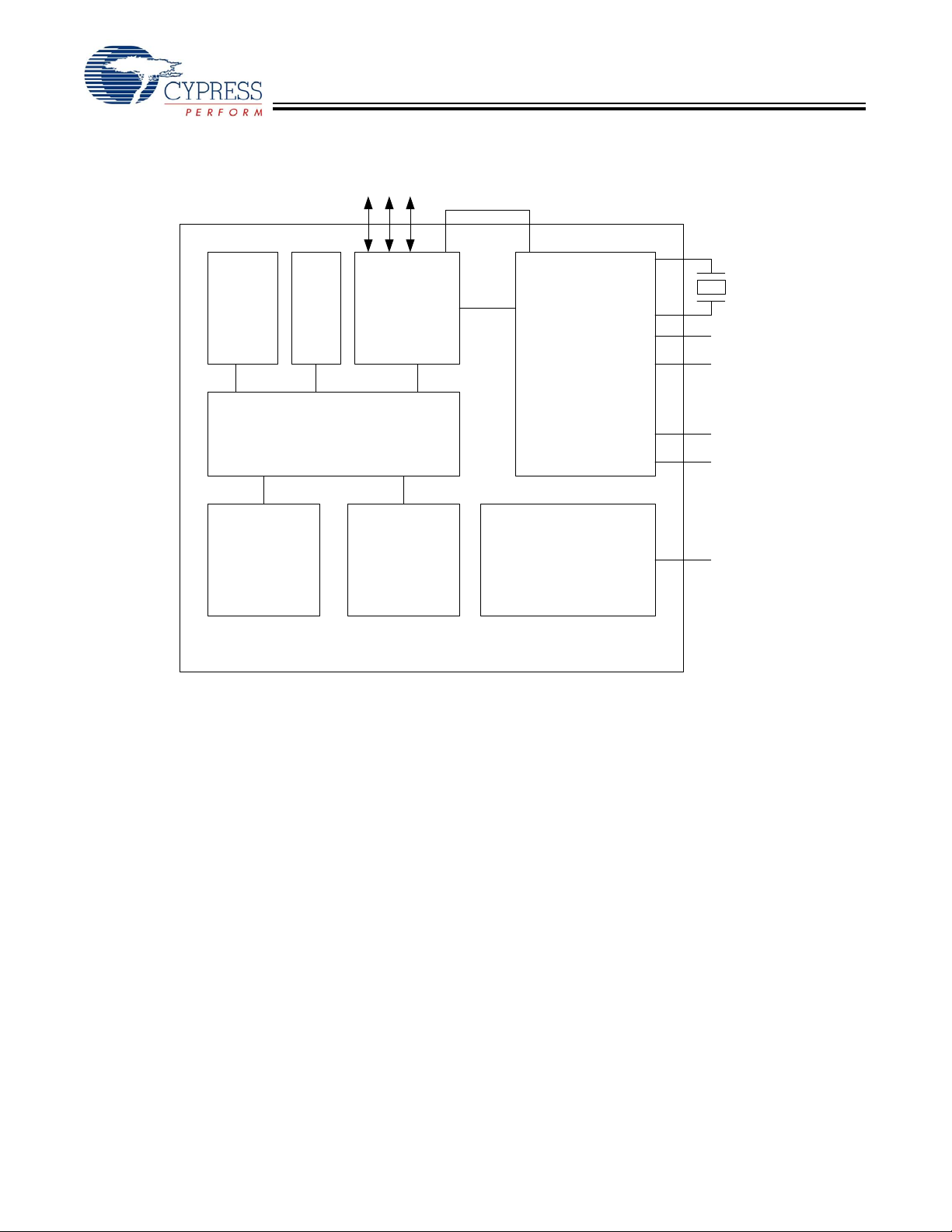
PRoC Block Diagram
CYWUSB6953
8KB Flash
Digital PSoC
Block Array
P0 P1 P2
512B
SRAM
PSoC M8C Core
Analog PSoC
IO Ports
Block Array
IRQ, MISO
2.4-GHz WirelessUSB
Radio Transceiver
System Resources
Clocks, I2C, POR, Ref
X13_OUT
PACTL
RFIN
RFOUT
XRES
Figure 1. PROC Block Diagram
Functional Overview
The CYWUSB6953 is a complete Radio System-on-Chip
device, enabling many simple RF systems to be implemented
with a single device and a handful of discrete components. The
CYWUSB6953 is designed to implement low cost wireless
systems operating in the worldwide 2.4-GHz Industrial, Scientific, and Medical (ISM) frequency band (2.400 GHz–2.4835
GHz).
The radio meets the following world-wide regulatory requirements:
• Europe
• ETSI EN 301 489-1 V1.4.1
• ETSI EN 300 328-1 V1.3.1
•North America
• FCC CFR 47 Part 15
• Japan
• ARIB STD-T66
The microcontroller is a powerful mixed-signal array. It has
highly reconfigurable and flexible digital and analog blocks.
The microcontroller core is the M8C 8-bit engine that supports
a rich instruction set. It contains 512 Bytes of data SRAM and
8 Kbytes code Flash memory. Full data on the microcontroller
can be found in the CY8C21534 data sheet and the PSo C™
Technical Reference Manual
The radio is a high-performance 2.4-GHz transceiver with a
fully integrated DSSS baseband. The radio and baseband are
both code and frequency agile. Protocols supporting
frequency agile direct-spread interference avoidance
algorithms such as WirelessUSB are fully compatible with this
radio. Full data on the radio can be found in the CYWUSB6935
data sheet.
Radio Data Rate Considerations
The PSoC Designer tool provides a software-based SPI User
Module for control of the radio portion of the PRoC. Therefore,
there is a direct relationship between CPU clock speed and
supportable radio data rate. For operation of CPU clock rates
less than 12 MHz, radio data rate must be set to 16 Kbps. Also
note that for operation at V
be set to 3 MHz per the CY8C21534 data sheet. Therefore, at
operation below 3V, the radio data rate must be set to 16 Kbps.
< 3.0V , the CPU clock rate must
CC
Document #: 38-16017 Rev. *D Page 2 of 7
CYWUSB6953
Pin Descriptions
Pin QFN Name Type Die Description
Analog RF
47 RFIN Radio Modulated RF Signal Received
2 RFOUT Radio Modulated RF Signal to be Transmitted
Crystal/PA Control
38 X13 I Radio Crystal Input
37 X13IN I Radio Crystal Input
24 X13OUT O Radio Reference Clock Output
35 PACTL IO Radio External Power Amplifier Control. Pull-down or make output
Reserved
23, 25 MISO IO Radio,
MCU
17, 21 IRQ IO Radio,
MCU
Microcontroller Digital/Analog
13 P0[0] IO/M MCU Analog Column Mux Input
14 P0[2] IO/M MCU Analog Column Mux Input
41 P1[0] IO/M MCU I2C Serial Data (SDA)
36 P1[1] IO/M MCU I2C Serial Clock (SCL)
42 P1[2] IO/M MCU
44 P1[4] IO/M MCU Optional External Clock Input (EXT-CLK)
34 P1[5] IO/M MCU I2C Serial Data (SDA)
6 P1[6] IO/M MCU
33 P1[7] IO/M MCU I2C Serial Clock (SCL)
8 P2[0] IO/M MCU Direct Switched Capacitor Block Input
31 P2[1] IO/M MCU Direct Switched Capacitor Block Input
9 P2[2] IO/M MCU Direct Switched Capacitor Block Input
30 P2[3] IO/M MCU Direct Switched Capacitor Block Input
10 P2[4] IO/M MCU
29 P2[5] IO/M MCU
12 P2[6] IO/M MCU
28 P2[7] IO/M MCU
7 XRES I MCU Active HIGH External Reset with Internal Pull-down
Power and Ground
4, 11, 15, 18, 26, 27,
32, 39, 40, 43, 45
1, 3, 5, 46, 48 GND Ground Connection
PADDLE GND Ground Connection
19, 20 RSVD Connect to Ground
16, 22, NC No Connect
V
CC
Radio SPI Master In, Slave Out. Connect pins 23 and 25 on the
application board
Radio Interrupt. Connect pins 17 and 21 on the application board
Supply Voltage
Document #: 38-16017 Rev. *D Page 3 of 7

Application Example
CYWUSB6953
Document #: 38-16017 Rev. *D Page 4 of 7

CYWUSB6953
PRoC Absolute Maximum Ratings
Parameter Description Min. Typ. Max. Unit
T
STG
T
A
V
dd
V
IO
V
IOZ
I
MIO
ESD Elec trostatic Discharge Voltage (Other) 1600 V
I
LU
PRoC Operating Conditions
Parameter Description Min. Typ. Max. Unit
V
CC
TA Ambient Temperature 0 25 70 °C
PRoC DC Electrical Characteristics
Parameter Description Min. Typ. Max. Unit
V
CC
I
CC
RX I
CC
TX I
CC
SYNTH SETTLE ICCCurrent Consumption with Synthesizer on, No Transmit
IDLE I
CC
I
SLEEP
Storage Temperature –55 100 °C
Ambient Temperature with Power Applied 0 70 °C
Supply Voltage on VCC Relative to VSS –0.3 3.9 V
DC Voltage to Logic Inputs –0.3 V
DC Voltage Applied to Outputs in High-Z State –0.3 V
+ 0.3 V
CC
+ 0.3 V
CC
Maximum Current into Any Port Pin –25 50 mA
Latch-up Current 200 mA
Supply Voltage 2.7 3 3.6 V
Supply Voltage 2.7 3 3.6 V
Supply Current (Radio in Power Down) 1.7 2 mA
Supply Current Radio Receive 61.3 mA
Supply Current Radio Transmit 74.7 mA
33.0 mA
or Receive
Supply Current Radio Idle 5 mA
Sleep Mode Supply Current 3 20 µA
Ordering Information
Part Number Radio Package Name Package Type Operating Range
CYWUSB6953-48LFXC Transceiver 48 QFN Pb-Free 48 Quad Flat No Lead Package Commercial
Document #: 38-16017 Rev. *D Page 5 of 7

Package Diagram
N
1
0.80 DIA.
2
TOP VIEW
6.90
7.10
6.70
6.80
48-Lead QFN 7 × 7 mm LF48A
0.08
0.05 MAX.
0.20 REF.
C
SEATING
PLANE
6.70
6.80
6.90
7.10
1.00 MAX.
0.80 MAX.
0°-12°
SIDE VIEW
C
0.30-0.45
CYWUSB6953
X
0.23±0.05
E-PAD
Y
0.50
5.45
5.55
BOTTOM VIEW
PIN1 ID
0.20 R.
N
1
2
0.45
5.45
5.55
0.42±0.18
(4X)
DIMENSIONS IN mm MIN.
MAX.
REFERENCE JEDEC MO-220
PKG. WEIGHT 0.13 gms
E-PAD SIZE PADDLE SIZE
(X, Y MAX.)
5.1 X 5.1
5.3 X 5.3
3.8 X 3.8 4.0 X 4.0
51-85152-*B
WirelessUSB, PSoC, and PRoC are trademarks of Cypress Se miconductor Corporation. All products and company names
mentioned in this document may be the trademarks of their respective holders.
Document #: 38-16017 Rev. *D Page 6 of 7
© Cypress Semiconductor Corporation, 2006. The information contained herein is subject to chan ge without notice. Cypress Semiconductor Corporation assumes no responsibility for the u se
of any circuitry other than circuitry embodied in a Cypress product. Nor does it convey or imply any license under patent or other rights. Cypress products are not warranted nor intended to be
used for medical, life support, life saving, critical control or safety applications, unless pursuant to an express written agreement with Cypress. Furthermore, Cyp ress does not a uthorize its
products for use as critical components in life-support systems where a malfunction or failure may reasonably be expected to result in significant injury to the user. The inclusion of Cypress
products in life-support systems application implies that the manufacturer assumes all risk of such use and in doing so indemnifies Cypress against all charges.

CYWUSB6953
Document History Page
Document Title: CYWUSB6953 WirelessUSB™ PRoC™ Flash Programmable MCU + Radio
Document Number: 38-16017
REV.
ECN
No.
** 329973 See ECN BON New data sheet
*A 337935 See ECN BON In th e Feature Section, changed “90 dBm receive sensitivity” to “– 90 dBm receive
*B 380254 See ECN BON Updated the PRoC DC Electrical Characteristics. Changed “– 90 dBm receive sensi-
*C 392781 See ECN BON Added the Radio Data Rate Considerations section
*D 495870 See ECN OYR Took off the photograph of the chip from the first page
Issue
Date
Orig. of
Change Description of Change
sensitivity”, and “13 MHz crystal clock” to “13 MHz crystal clock”
In the Functional Overview, changed “CYWUSB6934” to “CYWUSB6935”
In the Application Example, changed “ISSP” to “Programming Interface”
tivity” to “– 95 dBm receive sensitivity” in the Feature section. Removed lead-free part
offering. Changed supported CPU clock from 24 MHz to 12 MHz
Added Pb-free part numbers
Took off parts with lead
Quad flat package to QFN
Named Variables in Table
Document #: 38-16017 Rev. *D Page 7 of 7
 Loading...