


CYWUSB6935
WirelessUSB™ LR 2.4-GHz DSSS Radio SoC
1.0 Features
• 2.4-GHz radio transceiver
• Operates in the unlicensed Industrial, Scientific, and
Medical (ISM) band (2.4 GHz–2.483 GHz)
• –95-dBm receive sensitivity
• Up to 0dBm output power
• Range of up to 50 meters or more
• Data throughput of up to 62.5 kbits/sec
• Highly integrated low cost, minimal number of external
components required
• Dual DSSS reconfigurable baseband correlators
• SPI microcontroller interface (up to 2-MHz data rate)
• 13-MHz input clock operation
• Low standby current < 1 µA
• Integrated 32-bit Manufacturing ID
• Operating voltage from 2.7V to 3.6V
• Operating temperature from –40° to 85°C
• Offered in a small footprint 48 QFN
2.0 Functional Description
The CYWUSB6935 transce iver is a single-chi p 2.4-GHz Direct
Sequence Spread Spectrum (DSSS) Gaussian Frequency
Shift Keying (GFSK) baseband modem radio that connects
directly to a microcontroller via a simple serial peripheral
interface.
The CYWUSB6935 is offered in an industrial temperature
range 48-pin QFN and a commercial temperature range 48pin QFN.
3.0 Applications
• Building/Home Automation
—Climate Control
—Lighting Control
—Smart Appliances
—On-Site Paging Systems
—Alarm and Security
• Industrial Control
—Inventory Managem ent
—Factory Automation
—Data Acquisition
• Automatic Meter Reading (AMR)
• Transportation
—Diagnostics
—Remote Keyless Entry
•Consumer / PC
—Locator Alarms
—Presenter Tools
—Remote Controls
—Toys
DIOVAL
DIO
GFSK
Modulator
GFSK
Demodulator
RFOUT
RFIN
IRQ
SS
SCK
MISO
MOSI
RESET
PD
Digital
SERDES
A
SERDES
B
X13
X13IN
DSSS
Baseband
A
DSSS
Baseband
B
Synthesizer
X13OUT
Figure 3-1. CYWUSB6935 Simplified Block Diagram
Cypress Semiconductor Corporation • 3901 North First Street • San Jose, CA 95134 • 408-943-2600
Document 38-16008 Rev. *A Revised October 28, 2004

CYWUSB6935
3.1 Applications Support
The CYWUSB6935 is supported by both the CY3632
WirelessUSB Developmen t Kit and th e CY3635 W ireles sUSB
N:1 Development Kit. The CY3635 development kit provides
all of the materials and documents needed to cut the cord on
multipoint to poin t and point-to-p oint low ban dwidth, high node
density applications including four small form-factor sensor
boards and a hub board th at conn ect s to Wi reless USB LR RF
module boards, a software app lication that gra phically demo nstrates the multipoint to point protocol, comprehensive
WirelessUSB protocol code examples and all of the
associated schematics, gerber files and bill of materials. The
WirelessUSB N:1 Development Kit is also supported by the
WirelessUSB Listener Tool.
4.0 Functional Overview
The CYWUSB6935 provides a complete SPI-to-a ntenna radio
modem. The CYWUSB6935 is designed to implement
wireless devices operating in the worldwide 2.4-GHz Industrial, Scientific, and Medical (ISM) frequen cy ba nd (2 .40 0G Hz
- 2.4835GHz). It is in tended for sys tems com pliant with worl dwide regulations covered by ETSI EN 301 489-1 V1.4 .1, ETSI
EN 300 328-1 V1.3.1 (Europ ean Countries); FCC CFR 47 Part
15 (USA and Industry Canada) and ARIB STD-T66 (Japan).
The CYWUSB6935 contains a 2.4-GHz radio transceiver, a
GFSK modem, and a dual DSSS reconfigurable baseband.
The radio and baseband are both code- and frequency-agile.
Forty-nine spreading codes selected for optimal performance
(Gold codes) are supported across 78 1-MHz channels
yielding a theoretical spectral capacity of 3822 channels. The
CYWUSB6935 supports a range of up to 50 meters or more.
4.1 2.4-GHz Radio
The receiver and transmitter are a single-conversion, lowIntermediate Frequency (low-IF) architecture with fully
integrated IF channel matched filters to achieve high performance in the presence of interference. An integrated Power
Amplifier (P A) provide s an output power control range of 30 dB
in seven steps.
Table 4-1. Internal PA Output Power Step Table
P A Setting T ypical Output Power (dBm)
70
6–2.4
5–5.6
4–9.7
3–16.4
2–20.8
1–24.8
0–29.0
Both the receiver and transmitter integrated Voltage
Controlled Oscillator (VCO) and synthes izer have the ag ility to
cover the complete 2.4-GHz GFSK radio transmitter ISM
band. The synthesizer provides the frequency-hopping local
oscillator for the transmitter and receiver. The VCO loop filter
is also integrated on-chip.
4.2 GFSK Modem
The transmitter uses a DSP-based vector modulator to
convert the 1-MHz chips to an accurate GFSK carrier.
The receiver uses a fully integrated Frequency Modulat or (FM)
detector with automatic data slicer to demodulate the GFSK
signal.
4.3 Dual DSSS Baseband
Data is converted to DSSS chips by a digital spreader. Despreading is performed by an oversampled correlator. The
DSSS baseband cancels spurious noise and assembles
properly correlated data bytes.
The DSSS baseban d h as th ree ope rati ng modes: 64 chips /b it
Single Channel, 32 chips/bit Single Channel, and 32 chips/bit
Single Channel Dual Data Rate (DDR).
4.3.1 64 chips/bit Single Chan nel
The baseband supports a single data stream operating at
15.625 kbits/sec. The advantage of selecting this mode is its
ability to tolerate a noisy environment. This is because the
15.625 kbits/sec data stream utilizes the longest PN Code
resulting in the high es t p r oba bil ity for recovering packe t s ov er
the air. This mode can also be selected for systems requiring
data transmissi ons over lon ger ranges.
4.3.2 32 chips/bit Single Chan nel
The baseband supports a single data stream operating at
31.25 kbits/sec.
4.3.3 32 chips/bit Single Channel Dual Data Rate (DDR)
The baseband spread s bits in p airs and s upports a si ngle data
stream operating at 62.5 kbits/sec.
4.4 Serializer/Deserializer (SERDES)
CYWUSB6935 provides a data Serializer/Deserializer
(SERDES), which provides byte-level framing of transmit and
receive data. Bytes for transmission are loaded into the
SERDES and receive bytes are read from the SERDES via the
SPI interface. The SERDES provides double buffering of
transmit and receive dat a. While on e byte is bein g transmitted
by the radio the next byte can be written to the SERDES data
register insuring there are no breaks in transmitted data.
After a receive byte has been received it is loaded into the
SERDES data register and can be read at any time until the
byte is received, at which time the old contents of the
next
SERDES data register wil l be overwritten.
4.5 Application Interfaces
CYWUSB6935 has a fu lly sy nchronous SPI slave interface f or
connectivity to the application MCU. Configuration and byteoriented data transfer can be performe d over this interface. An
interrupt is provided to trigger real time events.
An optional SERDES Bypas s mode (DIO) is provided for a pplications that require a synchronous serial bit-oriented data
path. This interface is for data only.
Document 38-16008 Rev. *A Page 2 of 32

CYWUSB6935
4.6 Clocking and Power Management
A 13-MHz crystal is directly connected to X13IN and X13
without the need for external capacitors. The CYWUSB6935
has a progr ammable tr im capabil ity for ad justing t he on-ch ip
load capacitance supplied to the crystal. The Radio Frequency
(RF) circuitry has on-chip decoupling capacitors. The
CYWUSB6935 is powere d from a 2.7V to 3 .6V DC supply. The
CYWUSB6935 can be sh utdown to a fully static state u sing the
pin.
PD
Below are the requirements for the crystal to be directly
connected to X13IN and X13:
• Nominal Frequency: 13 MHz
• Operating Mode: Fundamen tal Mode
• Resonance Mode: Paralle l Reson ant
• Frequency Stability:
• Series Resistance: ≤ 100 ohms
• Load Capacitance: 10 pF
• Drive Level: 10uW–100 uW
± 30 ppm
4.7 Receive Signal Strength Indicator (RSSI)
The RSSI register (Reg 0x22) returns the relative signal
strength of the ON-channel signal power and can be used to:
1. Determine the connection quality
2. Determine the value of the noise floor
3. Check for a quiet channel before transmitting.
The internal RSSI voltage is sampled through a 5-bit analogto-digital converter (ADC). A state machine controls the
conversion process. Under normal conditions, the RSSI state
machine initia tes a c onv ersion when an ON-ch ann el ca rrie r i s
detected and remains abov e the noise floor for over 50uS. The
conversion produces a 5-bit value in the RSSI register (Reg
0x22, bits 4:0) along with a valid bit, RSSI register (Reg 0x22,
bit 5). The state machine then remains in HALT mode and
does not reset for a new conversion until the receive mode is
toggled off and on. Once a connection has been established,
the RSSI register can be read to determine the relative
connection quality of the channel . A RSSI register value lower
than 10 indicates that the received signal strength is low, a
value greater than 28 indicates a strong signal level.
To check for a quiet channel before transmitting, first set up
receive mode properl y and read the RSSI register (Reg 0 x22).
If the valid bit is zero, then force the Carrier Detect register
(Reg 0x2F, bit 7=1) to initiate an ADC conversion. Then, wait
greater than 50uS and read the RSSI register again. Next,
clear the Carrier Detect Register (Reg 0x2F, bit 7=0) and turn
the receiver OFF. Measuring the noise floor of a quiet channel
is inherently a 'noisy' process so, for best results, this
procedure should be repeated several times (~20) to compute
an average no ise floor level. A RSSI re gister value of 0-10
indicates a channel that is relatively quiet. A RSSI register
value greater than 10 indicates the channel is probably being
used. A RSSI register value greater than 28 indicates the
presence of a strong signal.
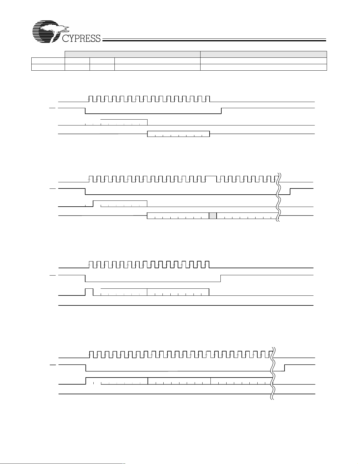
5.0 Application Interfaces
5.1 SPI Interface
The CYWUSB6935 has a four-wire SPI communication
interface between an a ppl ic ation MCU and one or more sl av e
devices. The SPI interface s upports single-byte an d multi- byte
serial transfers. The four-wire SPI communications interface
consists of Master Out-Slave In (MOSI), Master In-Slave Out
(MISO), Serial Clock (SCK), and Slave Select (SS
The SPI receives SCK from an application MCU on the SCK
pin. Data from the application MCU is shifted in on the MOSI
pin. Data to the application MCU is shifted out on the MISO
pin. The active-low Slave Selec t (SS)
initiate a SPI transfer.
The application MCU can initiate a SPI data transfer via a
multi-byte transact ion. T he first byt e is the Command/Add ress
byte, and the following bytes are the data bytes as shown in
Figure 5-1 through Figure 5-4. The SS
deasserted between bytes. The SPI communications is as
follows:
• Command Direction (bit 7) = “0 ” Enabl es SPI read transaction. A “1” enables SPI write transactions.
• Command Increment (b it 6) = “1” Enables SPI aut o address
increment. When se t, the addres s field automa tically i ncrements at the en d of each data byte in a bur s t access, ot herwise the same address is accessed.
• Six bits of address.
• Eight bits of data.
The SPI communications interface has a burst mechanism,
where the command byte can be followed by as many data
bytes as desired. A burst transaction is terminated by
deasserting the slave select (SS
tions, the application MCU must abide by the timing shown in
Figure 12-2.
The SPI communications i nter fac e s ing le re ad a nd b urs t rea d
sequences are shown in Figure 5-2 and Figure 5-3 , respectively.
The SPI communication s interfac e single write and burs t write
sequences are shown in Figure 5-4 and Figure 5-5 , respectively.
pin must be asserted to
signal should not be
= 1). For burst read transac-
).
Document 38-16008 Rev. *A Page 3 of 32
CYWUSB6935
Byte 1 Byte 1+N
Bit # 7 6 [5:0] [7:0]
Bit Name DIR INC Address Data
Figure 5-1. SPI Transaction Format
SCK
SS
addrcm d
A0A1A2A3A4A5
MOSI
DIR INC
00
data to mcu
MISO
D6D7
D0D1D2D3D4D5
Figure 5-2. SPI Single Read Sequence
SCK
SS
MOSI
MISO
DIR INC
01
addrcm d
A0A1A2A3A4A5
da ta to mcu
D6D7
1
D0D1D2D3D4D5
data to mcu
D6D7
1+N
D0D1D2D3D4D5
SCK
SS
MOSI
MISO
SCK
SS
MOSI
MISO
DIR INC
10
DIR INC
11
Figure 5-3. SPI Burst Read Sequence
addrcmd
D6D7
A0A1A2A3A4A5
data fro m mcu
Figure 5-4. SPI Single Write Sequence
addrcm d
da ta fro m mcu
D6D7
A0A1A2A3A4A5
D0D1D2D3D4D5
1
data from mcu
D0D1D2D3D4D5
D6D7
1+N
D0D1D2D3D4D5
Figure 5-5. SPI Burst Write Sequence
Document 38-16008 Rev. *A Page 4 of 32
CYWUSB6935
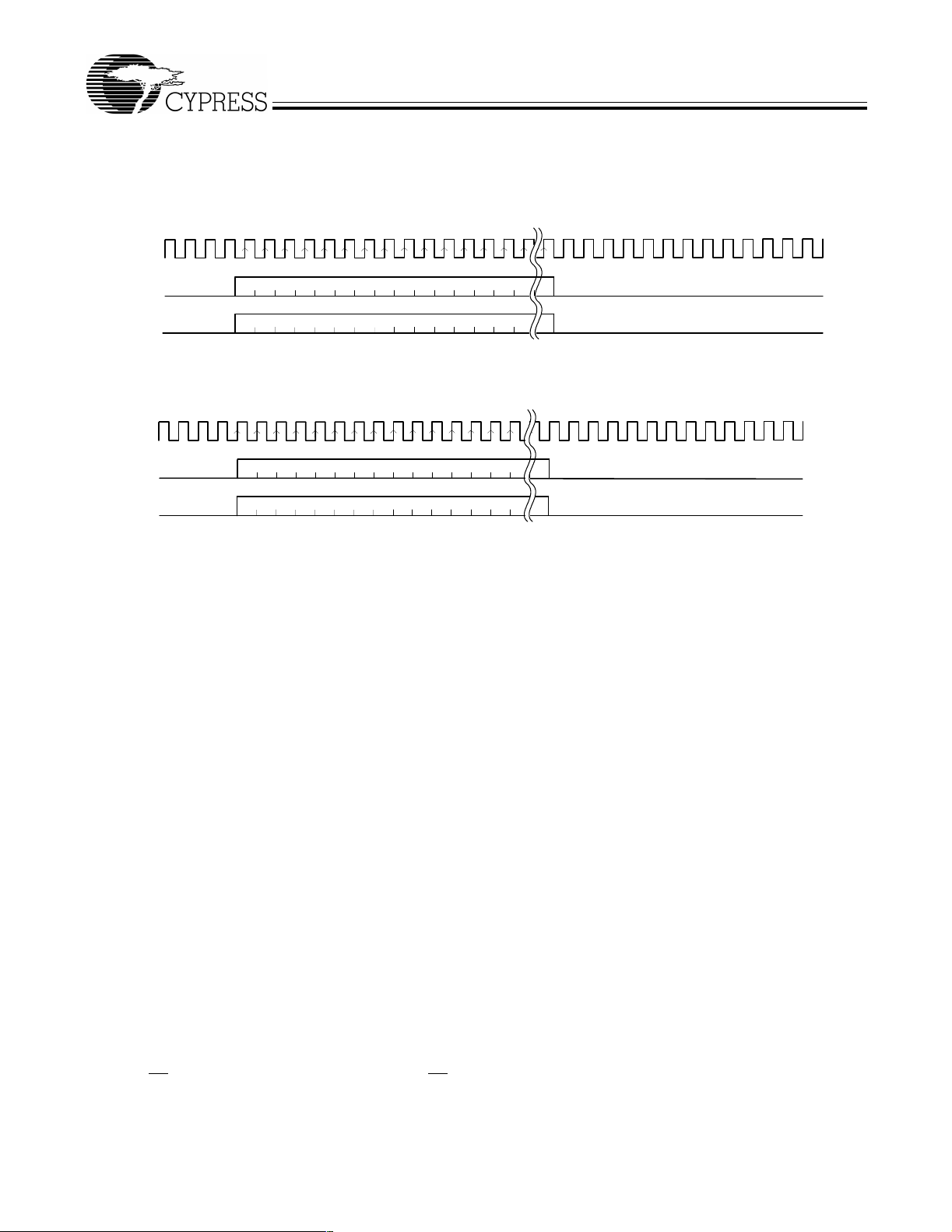
5.2 DIO Interface
The DIO communications interface is an optional SERDES
bypass data-only transfer interface. In receive mode, DIO and
DIOVAL are valid after the falling edge of IRQ, which clocks
IRQ
DIOVAL
v7v6v5v4v3v2
v9v8v1v0
data to mcu
DIO
d1d0
d7d6d5d4d3d2
Figure 5-6. DIO Receive Sequence
IRQ
DIOVAL
v1v0
v9v8
v7v6v5v4v3v2
data from mcu
DIO
d1d0
d7d6d5d4d3d2
Figure 5-7. DIO Transmit Sequence
the data as shown in
Figure 5-6. In transmit mode, DIO and
DIOVAL are sampled on the falling edge of the IRQ, which
clocks the data as shown in
Figure 5-7. The application MCU
samples the DIO and DIOVAL on the rising edge of IRQ.
v...v14v1 3v12v11v10
d...d14d13d12d11d1 0d9d8
v...v1 4v13v12v11v10
d...d1 4d13d12d11d10d9d8
5.3 Interrupts
The CYWUSB6935 features thre e se t s o f interrup t s: trans mi t,
received, and a wake interrupt. These interrupts all share a
single pin (IRQ), but can be independently enabled/disabled.
In transmit mode, all receive interrupts are automatically
disabled, and in receive mode all transmit interrupts are
automatically disabled. However, the contents of the enable
registers are preserve d when swit ching between tran smit an d
receive modes.
Interrupts are ena bled and the st atus read thr ough 6 registers:
Receive Interrupt Enable (Reg 0x07), Recei ve Interrupt S t atus
(Reg 0x08), Transmit Interrupt Enable (Reg 0x0D), Transmit
Interrupt Status (Reg 0x0E), Wake Enable (Reg 0x1C), Wake
Status (Reg 0x1D).
If more than 1 interrupt is enabled at any time, it is necessary
to read the relevant interrupt st atus register to determine which
event caused the IRQ pin to assert. Even when a given
interrupt source is disabled, the status of the condition that
would otherwise cause an interrupt can be determined by
reading the appropriate int errupt st atus regis ter. It is therefore
possible to use th e devic es with out mak ing us e of the I RQ pin
at all. Firmware can poll the interrupt status register(s) to wait
for an event, rather than using the IRQ pin.
The polarity of all interrupt s can be s et by writing to the Co nfiguration register (Reg 0x05), and it is possible to configure the
IRQ pin to be o pen drain (if a ctive low) o r open source (if active
high).
5.3.1 Wake Interrupt
When the PD pin is low, the oscillator is stopped. After PD is
deasserted, the oscillator takes time to start, and until it has
done so, it is not safe to use the SPI interface. The wake
interrupt indicates that the oscillator has started, and that the
device is ready to receive SPI transfers.
The wake interrupt is enabled by setting bit 0 of the Wake
Enable register (Reg 0x1C, bit 0=1). Whether or not a wake
interrupt is pendin g is indicated by the state of bit 0 of the Wake
Status register (Reg 0x1D, bit 0). Reading the Wake Status
register (Reg 0x1D) clears the interrupt.
5.3.2 T ran sm it Inte rrupts
Four interrupts a re p rov id ed t o fl ag the oc cu rren ce of t rans m it
events. The interrupts are enabled by writing to the Transmit
Interrupt Enable register (Reg 0x0D), and their status may be
determined by reading the Transmit Interrupt Status register
(Reg 0x0E). If more than 1 interrupt i s enabled , it is neces sary
to read the Transmit Interrupt Status register (Reg 0x0E) to
determine which event caused the IRQ pin to assert.
The function and operatio n of these interrupts are des cribed in
detail in
Section 7.0.
5.3.3 Receive Interrupts
Eight interrupts are provided to flag the occurrence of receive
events, four each fo r SERDES A and B. In 64 c hips /bit and 3 2
chips/bit DDR modes, only the SERDES A interrupts are
available, and the SERDES B interrupts will never trigger,
even if enabled. The interrupts are enabled by writing to the
Receive Interrupt Enab le regis ter (Reg 0x 07), and their st atu s
may be determin ed by reading the Rece ive Interrupt Status
register (Reg 0x08 ). If m ore th an on e int errup t i s en abl ed, it i s
necessary to read the Receive Interrupt Status register (Reg
0x08) to determine whic h e ven t ca us ed th e IRQ pin to as se rt.
The function and operatio n of these interrupts are des cribed in
detail in
Section 7.0.
Document 38-16008 Rev. *A Page 5 of 32
CYWUSB6935
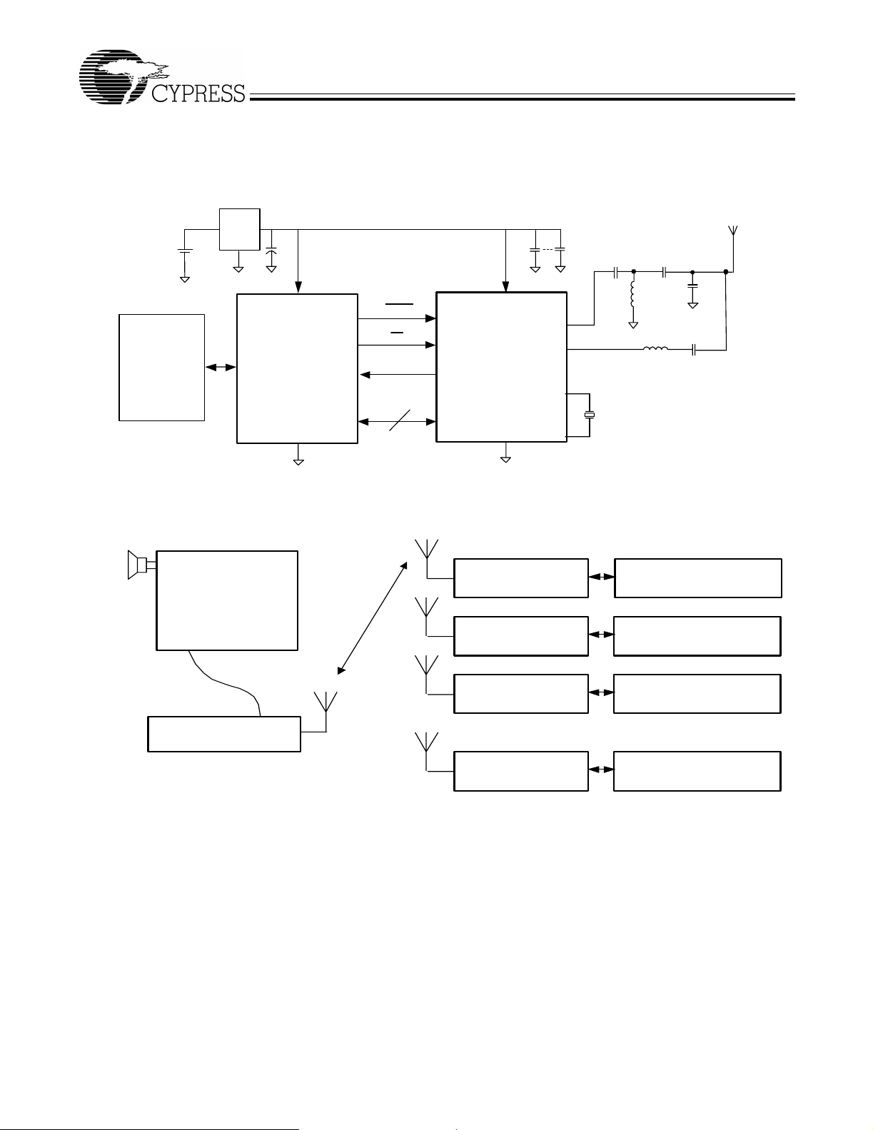
6.0 Application Examples
Figure 6-1 shows a block di agram example of a typ ical battery
powered device using the CYWUSB6935 chip.
Battery
Application
Hardware
LDO/
DC2DC
+
-
PSoC
8-bit MCU
Figure 6-1. CYWUSB6935 Battery Powered Device
Vcc
3.3 V
RESET
PD
IRQ
SPI
4
Figure 6-2 shows an application example of a WirelessUSB
LR alarm system where a single hub node is connected to an
alarm panel. The hub node wirelessly receives information
from multiple sensor nodes in order to control the alarm panel.
2.0 pF
PCB Tr ace
Wig g l e
Antenna
1.2 pF
27 pF
Vcc
RFOUT
Wir elessUSB LR
RFIN
0.1µF
2.0 pF
13M Hz
Crystal
3.3 nH
2.2 nH
ALARM PANEL
R
S
2
3
2
W irelessUSB LR +
PSoC
W irelessUSB LR
W irelessUSB LR
W irelessUSB LR
W irelessUSB LR PSoC + KEYPAD
Figure 6-2. WirelessUSB LR Alarm Syste m
PSoC + SMOKE
DETECTOR
PSoC + MOTION
DETECTOR
PSoC + DOOR
SENSOR
…
Document 38-16008 Rev. *A Page 6 of 32

CYWUSB6935
7.0 Register Descriptions
Table 7-1 displays the list of registers inside the
CYWUSB6935 that are addressable through the SPI interfac e.
All registers are read and writable, except where noted.
Table 7-1. CYWUSB6935 Register Map
Register Name Mnemonic
Revision ID REG_ID 0x00 9 0x07 RO
Reserved RESERVED 0x01 8 0x00 RW
Reserved RESERVED 0x02 8 0x00 RW
Control REG_CONTROL 0x03 9 0x00 RW
Data Rate REG_DATA_RATE 0x04 10 0x00 RW
Configuration REG_CONFIG 0x05 11 0x01 RW
SERDES Control REG_SERDES_CTL 0x06 11 0x03 RW
Receive SERDES Interrupt Enable REG_RX_INT_EN 0x07 12 0x00 RW
Receive SERDES Interrupt Status REG_RX_INT_STAT 0x08 13 0x00 RO
Receive SERDES Data A REG_RX_DATA_A 0x09 14 0x00 RO
Receive SERDES Valid A REG_RX_VALID_A 0x0A 14 0x00 RO
Receive SERDES Data B REG_RX_DATA_B 0x0B 14 0x00 RO
Receive SERDES Valid B REG_RX_VALID_B 0x0C 14 0x00 RO
Transmit SERDES Interrupt Enable REG_TX_INT_EN 0x0D 15 0x00 RW
Transmit SERDES Interrupt Status REG_TX_INT_STAT 0x0E 15 0x00 RO
Transmit SERDES Data REG_TX_DATA 0x0F 16 0x00 RW
Transmit SERDES Valid REG_TX_VALID 0x10 16 0x00 RW
PN Code REG_PN_CODE 0x18–0x11 16
Threshold Low REG_THRESHOLD_L 0x19 17 0x08 RW
Threshold High REG_THRESHOLD_H 0x1A 17 0x38 RW
Wake Enable REG_WAKE_EN 0x1C 18 0x00 RW
Wake Status REG_WAKE_STAT 0x1D 18 0x01 RO
Analog Control REG_ANALOG_CTL 0x20 18 0x04 RW
Channel REG_CHANNEL 0x21 19 0x00 RW
Receive Signal Strength Indicator REG_RSSI 0x22 19 0x00 RO
Power Control REG_PA 0x23 19 0x0 0 RW
Crystal Adjust REG_CRYSTAL_ADJ 0x24 20 0x00 RW
VCO Calibration REG_VCO_CAL 0x26 20 0x00 RW
Reg Power Control REG_PWR_CTL 0x2E 21 0x00 RW
Carrier Detect REG_CARRIER_DETECT 0x2F 21 0x00 RW
Clock Manual REG_CLOCK_MANUAL 0x32 21 0x00 RW
Clock Enable REG_CLOCK_ENABLE 0x33 21 0x00 RW
Synthesizer Lock Count REG_SYN_LOCK_CNT 0x38 22 0x64 RW
Manufacturing ID REG_MID 0x3C–0x3F 22 – RO
[1]
CYWUSB6935
Address Page Default Access
0x1E8B6A3DE0E9B222
RW
Note:
1. All registers are accessed Little Endian.
Document 38-16008 Rev. *A Page 7 of 32

CYWUSB6935
Addr: 0x00 REG_ID Default: 0x07
76543210
Silicon ID Product ID
Figure 7-1. Revision ID Register
Bit Name Description
7:4 Silicon ID These are the Silicon ID revision bits. 0000 = Rev A, 0001 = Rev B, etc. These bits are read-only.
3:0 Product ID These are the Product ID revision bits. Fixed at value 0111. These bits are read-only.
Addr: 0x01 RESERVED Default: 0x00
76543210
Reserved
Figure 7-2. Reserved
Bit Name Description
7:0 Reserved These bits are reserved and should be written with zeroes.
Addr: 0x02 RESERVED Default: 0x00
76543210
Reserved
Figure 7-3. Reserved
Bit Name Description
7:0 Reserved These bits are reserved and should be written with zeroes.
Document 38-16008 Rev. *A Page 8 of 32

CYWUSB6935
Addr: 0x03 REG_CONTROL Default: 0x00
76543210
RX
Enable
TX
Enable
PN Code
Select
Auto Syn
Count Select
Auto Internal PA
Disable
Internal PA
Enable
Reserved Reserved
Figure 7-4. Control
Bit Name Description
7 RX Enable The Receive Enable bit is used to place the IC in receive mode.
6 TX Enable The Transmit Enable bit is used to place the IC in transmit mode.
5 PN Code Select The Ps eudo-Noise Code Select bit selects between the upper or lower half of the 64 chips/bit PN code.
4 Auto Syn Count
Select
3 Auto Internal PA
Disable
2 Internal PA
Enable
1 Reserv ed This bit is reserved and should be written with a one.
0 Reserv ed This bit is reserved and should be written with a zero.
1 = Receive Enabled
0 = Receive Disabled
1 = Transmit Enabled
0 = Transmit Disabled
1 = 32 Most Significant Bits of PN code are used
0 = 32 Least Significant Bits of PN code are used
This bit applies only when the Code Width bit is set to 32 chips/bit PN codes (Reg 0x04, bit 2=1).
The Auto Synthesizer Count Select bit is used to select the method of determining the settle ti me of the synthesizer .
The two options are a programmable settle time based on the value in Syn Lock Count register (Reg 0x38), in units
of 2us, or by the auto detection of the synthesizer lock.
1 = Synthesizer settle time is based on a count in Syn Lock Count register (Reg 0x38)
0 = Synthesizer settle time is based on the internal synthesizer lock signal
It is recommended that the Auto Syn Count Select bit is set to 1 as that guarantees a consistent settle time for the
synthesizer.
The Auto Internal PA Disable bit is used to determine the method of controlling the Internal Power Amplifier. The
two options are automatic control by the baseband or by firmware through register writes. For external PA usage,
please see the description of the REG_ANALOG_CTL register (Reg 0x20).
1 = Register controlled Internal PA Enable
0 = Auto controlled Internal PA Enable
When this bit is set to 1, the enabled state of the Internal PA is directly controlled by bit Internal PA Enable (Reg
0x03, bit 2). It is recommended that this bit is set to 0, leaving
The Internal PA Enable bit is used to enable or disable the Internal Power Amplifier.
1 = Internal Power Amplifier Enabled
0 = Internal Power Amplifier Disabled
This bit only applies when the Auto Internal P A Disable bit is selected (Reg 0x03, bit 3=1), otherwise this bit is don’t
care.
the PA control to the baseband.
Document 38-16008 Rev. *A Page 9 of 32

CYWUSB6935
Addr: 0x04 REG_DATA_RATE Default: 0x00
76543210
Reserved Code Width Data Rate Sample Rate
Figure 7-5. Data Rate
Bit Name Description
7:3 Reserved
[2]
2
Code Width The Code Width bit is used to select between 32 chips/bit and 64 chips/bit PN codes.
[2]
Data Rate The Data Rate bit allows the user to select Double Data Rate mode of operation which delivers a raw data rate of
1
[2]
Sample Rate The Sample Rate bit allows the use of the 12x sampling when using 32 chips/bit PN codes and Normal Data Rate.
0
These bits are reserved and should be written with zeroes.
1 = 32 chips/bit PN codes
0 = 64 chips/bit PN codes
The number of chips/bit used impacts a number of factors such as data throughput, range and robustness to interference. By choosing a 32 chips/bit PN-code, the data throughput can be doubled or even quadrupled (when double
data rate is set). A 64 chips/bit PN code offers improved range over its 32 chips/bit counterpart as well as more
robustness to interference. By selecting to use a 32 chips/bit PN code a number of other register bits are impacted
and need to be addressed. These are PN Code Select (Reg 0x03, bit 5), Data Rate (Reg 0x04, bit 1), and Sample
Rate (Reg 0x04, bit 0).
62.5kbits/sec.
1 = Double Data Rate - 2 bits per PN code (No odd bit transmissions)
0 = Normal Data Rate - 1 bit per PN code
This bit is applicable only when using 32 chips/bit PN codes which can be selected by setting the Code Width bit (Reg
0x04, bit 2=1). When using Double Data Rate, the raw data throughput is 62.5 kbits/sec because every 32 chips/bit
PN code is interpreted as 2 bits of data. When using this mode a single 64 chips/bit PN code is placed in the PN code
register. This 64 chips/bit PN code is then split into two and used by the baseband to offer the Double Data Rate
capability.
enables the user to potentially correlate data using two differing 32 chips/bit PN codes.
Using 12x oversampling improves the correlators receive sensitivity. When using 64 chips/bit PN codes or Double Data
Rate this bit is don’t care. The only time when 12x oversampling can be selected is when a 32 chips/bit PN code is
being used with Normal Data Rate.
When using Normal Data Rate, the raw data throughput is 32kbits/sec. Additionally, Normal Data Rate
1 = 12x Oversampling
0 = 6x Oversampling
Note:
2. The following Reg 0x04, bits 2:0 values are no t valid:
• 001–Not Valid
• 010–Not Valid
• 011–Not Valid
• 111–Not Valid
Document 38-16008 Rev. *A Page 10 of 32

CYWUSB6935
Addr: 0x05 REG_CONFIG Default: 0x01
76543210
Reserved IRQ Pin Select
Figure 7-6. Configurat ion
Bit Name Description
7:2 Reserved These bits are reserved and should be written with zeroes.
1:0 IRQ Pin Select The Interrupt Request Pin Select bits are used to determine the drive method of the IRQ pin.
11 = Open Source (IRQ asserted = 1, IRQ deasserted = Hi-Z)
10 = Open Drain (IRQ asserted = 0, IRQ deasserted = Hi-Z)
01 = CMOS (IRQ asserted = 1, IRQ deasserted = 0)
00 = CMOS Inverted (IRQ asserted = 0, IRQ deasserted = 1)
Addr: 0x06 REG_SERDES_CTL Default: 0x03
76543210
Reserved SERDES
Enable
EOF Length
Figure 7-7. SERDES Control
Bit Name Descripti on
7:4 Reserved These bits are reserved and should be written with zeroes.
3 SERDES Enable The SERDES Enable bit is used to switch between bit-serial mode and SERDES mode.
2:0 EOF Length The End of Frame Length bits are used to set the number of sequential bit times for an inter-frame gap without
1 = SERDES enabled
0 = SERDES disabled, bit-serial mode enabled
When the SERDES is enabled data can be written to and read from the IC one byte at a time, through the use of
the SERDES Data registers. The bit-serial mode requires bits to be written one bit at a time through the use of
the DIO/DIOVAL pins, refer to section 3.2. It is recommended that SERDES mode be used to avoid the need to
manage the timing required by the bit-serial mode.
valid data before an EOF event will be generated. When in receive mode and a valid bit has been received the
EOF event can then be identified by the number of bit times that expire without correlating any new data. The
EOF event causes data to be moved to the proper SERDES Data Register and can also be used to generate
interrupts. If 0 is the EOF length, an EOF condition will occur at the first invalid bit after a valid reception.
Document 38-16008 Rev. *A Page 11 of 32

CYWUSB6935
Addr: 0x07 REG_RX_INT_EN Default: 0x00
76543210
Underflow B Overflow B EOF B Full B Underflow A Overflow A EOF A Full A
Figure 7-8. Receive SERDES Interrupt Enable
Bit Name Description
7 Underflow B The Underflow B bit is used to enable the interrupt associated with an underflow condition with the Receive SERDES
6 Overflow B The Overflow B bit is used to enable the interrupt associated with an overflow condition with the Receive SERDES
5 EOF B The End of Frame B bit is used to enable the interrupt associated with the Channel B Receiver EOF condition.
4 Full B The Full B bit is used to enable the interrupt associated with the Receive SERDES Data B register (Reg 0x0B) having
3 Underflow A The Underflow A bit is used to enable the interrupt associated with an underflow condition with the Receive SERDES
2 Overflow A The Overflow A bit is used to enable the interrupt associated with an overflow condition with the Receive SERDES
1 EOF A The End of Frame A bit is used to enable the interrupt associated with an End of Frame condition with the Channel
0 Full A The Full A bit is used to enable the interrupt associated with the Receive SERDES Data A register (0x09) having
Data B register (Reg 0x0B)
1 = Underflow B interrupt enabled for Receive SERDES Data B
0 = Underflow B interrupt disabled for Receive SERDES Data B
An underflow condition occurs when attempting to read the Receive SERDES Data B register (Reg 0x0B) when it is
empty.
Data B register (Reg 0x0B)
1 = Overflow B interrupt enabled for Receive SERDES Data B
0 = Overflow B interrupt disabled for Receive SERDES Data B
An overflow condition occurs when new received data is written into the Receive SERDES Data B register (Reg
0x0B) before the prior data is read out.
1 = EOF B interrupt enabled for Channel B Receiver
0 = EOF B interrupt disabled for Channel B Receiver
The EOF IRQ asserts during an End of Frame condition. End of Frame conditions occur after at least one bit has
been detected, and then the number of invalid bits in the frame exceeds the number in the EOF length field. If 0 is
the EOF length, and EOF condition will occur at the first invalid bit after a valid reception. This IRQ is cleared by
reading the receive status register
data placed in it.
1 = Full B interrupt enabled for Receive SERDES Data B
0 = Full B interrupt disabled for Receive SERDES Data B
A Full B condition occurs when data is transferred from the Channel B Receiver into the Receive SERDES Data B
register (Reg 0x0B). This could occur when a complete byte is received or when an EOF event occurs whether or
not a complete byte has been received.
Data A register (Reg 0x09)
1 = Underflow A interrupt enabled for Receive SERDES Data A
0 = Underflow A interrupt disabled for Receive SERDES Data A
An underflow condition occurs when attempting to read the Receive SERDES Data A register (Reg 0x09) when it is
empty.
Data A register (0x09)
1 = Overflow A interrupt enabled for Receive SERDES Data A
0 = Overflow A interrupt disabled for Receive SERDES Data A
An overflow condition occurs when new receive data is written into the Receive SERDES Data A register (Reg 0x09)
before the prior data is read out.
A Receiver.
1 = EOF A interrupt enabled for Channel A Receiver
0 = EOF A interrupt disabled for Channel A Receiver
The EOF IRQ asserts during an End of Frame condition. End of Frame conditions occur after at least one bit has
been detected, and then the number of invalid bits in a frame exceeds the number in the EOF length field. If 0 is the
EOF length, an EOF condition will occur at the first invalid bit after a valid reception. This IRQ is cleared by reading
the receive status register.
data written into it.
1 = Full A interrupt enabled for Receive SERDES Data A
0 = Full A interrupt disabled for Receive SERDES Data A
A Full A condition occurs when data is transferred from the Channel A Receiver into the Receive SERDES Data A
register (Reg 0x09). This could occur when a complete byte is received or when an EOF event occurs whether or
not a complete byte has been received.
Document 38-16008 Rev. *A Page 12 of 32

CYWUSB6935
Addr: 0x08 REG_RX_INT_STAT Default: 0x00
76543210
Valid B Flow Violation B EOF B Full B Valid A Flow Violation A EOF A Full A
Figure 7-9. Receive SE RDES Interrupt Status
Bit Name Description
7 Valid B The Valid B bit is true when all the bits in the Receive SERDES Data B register (Reg 0x0B) are valid.
1 = All bits are valid for Receive SERDES Data B
0 = Not all bits are valid for Receive SERDES Data B
When data is written into the Receive SERDES Data B register (Reg 0x0B) this bit is set if all of the bits within the
byte that has been written are valid. This bit cannot generate an interrupt.
6 Flow Violation B The Flow Violation B bit is used to signal whether an overflow or underflow condition has occurred for the Receive
5 EOF B The End of Frame B bit is used to signal whether an EOF event has occurred on the Channel B receive.
4 Full B The Full B bit is used to signal when the Receive SERDES Data B register (Reg 0x0B) is filled with data.
3 Valid A The Valid A bit is true when all of the bits in the Receive SERDES Data A Register (Reg 0x09) are valid.
2 Flow Violation A The Flow Violation A bit is used to signal whether an overflow or underflow condition has occurred for the Receive
1 EOF A The End of Frame A bit is used to signal whether an EOF event has occurred on the Channel A receive.
0 Full A The Full A bit is used to signal when the Receive SERDES Data A register (Reg 0x09) is filled with data.
SERDES Data B register (Reg 0x0B).
1 = Overflow/underflow interrupt pending for Receive SERDES Data B
0 = No overflow/underflow interrupt pending for Receive SERDES Data B
Overflow conditions occur when the radio loads new data into the Receive SERDES Data B register (Reg 0x0B)
before the prior data has been read. Underflow conditions occur when trying to read the Receive SERDES Data B
register (Reg 0x0B) when the register is
(Reg 0x08)
1 = EOF interrupt pending for Channel B
0 = No EOF interrupt pending for Channel B
An EOF condition occurs for the Channel B Receiver when receive has begun and then the number of bit times
specified in the SERDES Control register (Reg 0x06) elapse without any valid bits being received. This bit is cleared
by reading the Receive Interrupt Status register (Reg 0x08)
1 = Receive SERDES Data B full interrupt pending
0 = No Receive SERDES Data B full interrupt pending
A Full B condition occurs when data is transferred from the Channel B Receiver into the Receive SERDES Data B
register (Reg 0x0B). This could occur when a complete byte is received or when an EOF event occurs whether or
not a complete byte has been received.
1 = All bits are valid for Receive SERDES Data A
0 = Not all bits are valid for Receive SERDES Data A
When data is written into the Receive SERDES Data A register (Reg 0x09) this bit is set if all of the bits within the
byte that has been written are valid. This bit cannot generate an interrupt.
SERDES Data A register (Reg 0x09).
1 = Overflow/underflow interrupt pending for Receive SERDES Data A
0 = No overflow/underflow interrupt pending for Receive SERDES Data A
Overflow conditions occur when the radio loads new data into the Receive SERDES Data A register (Reg 0x09)
before the prior data has been read. Underflow conditions occur when trying to read the Receive SERDES Data A
register (Reg 0x09) when the register is empty. This bit is cleared by reading the Receive Interrupt Status register
(Reg 0x08)
1 = EOF interrupt pending for Channel A
0 = No EOF interrupt pending for Channel A
An EOF condition occurs for the Channel A Receiver when receive has begun and then the number of bit times
specified in the SERDES Control register (0x06) elapse without any valid bits being received. This bit is cleared by
reading the Receive Interrupt Status register (Reg 0x08).
1 = Receive SERDES Data A full interrupt pending
0 = No Receive SERDES Data A full interrupt pending
A Full A condition occurs when data is transferred from the Channel A Receiver into the Receive SERDES Data A
Register (Reg 0x09). This could occur when a complete byte is received or when an EOF event occurs whether or
not a complete byte has been received.
empty . This bit is cleared by reading the Receive Interrupt Status register
[3]
Note:
3. All status bits are set and readable in the registers regardless of IRQ enable status. This allows a polling scheme to be implemented without enabling IRQs. The
status bits are affected by TX Enable and RX Enable (Reg 0x03, bits 7:6). For example, the receive status will read 0 if the IC is not in receive mode. These
registers are read-only.
Document 38-16008 Rev. *A Page 13 of 32

CYWUSB6935
Addr: 0x09 REG_RX_DATA_A Default: 0x00
76543210
Data
Figure 7-10. Receive SERDES Data A
Bit Name Description
7:0 Data
Received Data for Channel A. The over-the-air received order is bit 0 followed by bit 1, followed by bit 2, followed by bit 3,
followed by bit 4, followed by bit 5, followed by bit 6, followed by bit 7. This register is read-only.
Addr: 0x0A REG_RX_VALID_A Default: 0x00
76543210
Valid
Figure 7-11. Receive SERDES Valid A
Bit Name Description
7:0 Valid
These bits indicate which of the bits in the Receive SERDES Data A register (Reg 0x09) are valid. A “1” indicates that the
corresponding data bit is valid for Channel A.
If the Valid Data bit is set in the Receive Interrupt Status register (Reg 0x08) all eight bits in the Receive SERDES Data A
register (Reg 0x09) are valid. Therefore, it is not necessary to read the Receive SERDES Valid A register (Reg 0x0A). This
register is read-only.
Addr: 0x0B RE G _RX_D ATA_B Default: 0x00
76543210
Data
Figure 7-12. Receive SERDES Data B
Bit Name Description
7:0 Data
Received Data for Channel B. The over-the-air received order is bit 0 followed by bit 1, followed by bit 2, followed by bit 3,
followed by bit 4, followed by bit 5, followed by bit 6, followed by bit 7. This register is read-only.
Addr: 0x0C REG_RX_VALID_B Default: 0x00
76543210
Valid
Figure 7-13. Receive SERDES Valid B
Bit Name Description
7:0 Valid
These bits indicate which of the bits in the Receive SERDES Data B register (Reg 0x0B) are valid. A “1” indicates that the
correspondi ng data bit is valid for Channel B.
If the Valid Data bit is set in the Receive Interrupt St atus register (0x08) all eight bits in the Receive SERDES Data B register
(Reg 0x0B) are valid. Therefore, it is not necessary to read the Receive SERDES Valid B register (Reg 0x0C). This register
is read-only.
Document 38-16008 Rev. *A Page 14 of 32

CYWUSB6935
Addr: 0x0D REG_TX_INT_EN Default: 0x00
76543210
Reserved Underflow Overflow Done Empty
Figure 7-14. Transmit SERDES Interrupt Enable
Bit Name Description
7:4 Reserved
3 Underflow
2 Overflow
1 Done The Done bit is used to enable the interrupt that signals the end of the transmission of data.
0 Empty The Empty bit is used to enable the interrupt that signals when
These bits are reserved and should be written with zeroes.
The Underflow bit is used to enable the interrupt associated with an underflow condition associated with the Transmit
SERDES Data register (Reg 0x0F)
1 = Underflow interrupt enabled
0 = Underflow interrupt disabled
An underflow condition occurs when attempting to transmit while the Transmit SERDES Data register (Reg 0x0F) does
not have any data.
The Overflow bit is used to enabled the interrupt associated with an overflow condition with the T ransmit SERDES Data
register (0x0F).
1 = Overflow interrupt enabled
0 = Overflow interrupt disabled
An overflow condition occurs when attempting to write new data to
before the preceding data has been transferred to the transmit shift register.
1 = Done interrupt enabled
0 = Done interrupt disabled
The Done condition occurs when the Transmit SERDES Data register (Reg 0x0F) has transmitted all of its data and
there is no more data for it to transmit.
the Transmit SERDES Data register (Reg 0x0F)
the Transmit SERDES register (Reg 0x0F) is empty.
1 = Empty interrupt enabled
0 = Empty interrupt disabled
The Empty condition occurs when the Transmit SERDES Data register (Reg 0x0F) is loaded into the transmit buffer
and it's safe to load the next byte
Addr: 0x0E REG_TX_INT_STAT Default: 0x00
76543210
Reserved Underflow Overflow Done Empty
Figure 7-15. Transmit SERDES Interrupt Status
Bit Name Description
7:4 Reserved These bits are reserved. This register is read-only.
3 Underflow The Underflow bit is used to signal when an underflow condition associated with the Transmit SERDES Data register
2 Overflow The Overflow bit is used to signal when an overflow condition associated with the Transmit SERDES Data register (0x0F)
1 Done The Done bit is used to signal the end of a data transmission.
0 Empty The Empty bit is used to signal when
Note:
4. All status bits are set and readable in the registers regardless of IRQ enable status. This allows a polling scheme to be implemented without enabling
IRQs. The status bits are affected by the TX Enable and RX Enable (Reg 0x03, bits 7:6). For example, the transmit status will read 0 if the IC is not in
transmit mode. These registers are read-only.
(Reg 0x0F) has occurred.
1 = Underflow Interrupt pending
0 = No Underflow Interrupt pending
This IRQ will assert during an underflow condition to the Transmit SERDES Data register (Reg 0x0F). An underflow occurs
when the transmitter is ready to sample transmit data, but there is no data ready in the Transmit SERDES Data register
(Reg 0x0F). This will only assert after the transmitter has transmitted at least one bit. This bit is cleared by reading the
Transmit Interrupt Status register (Reg 0x0E).
has occurred.
1 = Overflow Interrupt pending
0 = No Overflow Interrupt pending
This IRQ will assert during an overflow condition to the Transmit SERDES Data register (Reg 0x0F). An overflow occurs
when the new data is loaded into the Transmit SERDES Data register (Reg 0x0F) before the previous data has been sent.
This bit is cleared by reading the Transmit Interrupt Status register (Reg 0x0E).
1 = Done Interrupt pending
0 = No Done Interrupt pending
This IRQ will assert when the data is finished sending a byte of data and there is no more data to be sent. This will only
assert after the transmitter has transmitted as least one bit. This bit is cleared by reading the Transmit Interrupt Status
register (Reg 0x0E)
the Transmit SERDES Data register (Reg 0x0F) has been emptied.
1 = Empty Interrupt pending
0 = No Empty Interrupt pending
This IRQ will assert when the transmit serdes is empty. When this IRQ is asserted it is ok to write t o the Transmit SERDES
Data register (Reg 0x0F). Writing the Transmit SERDES Data register (Reg 0x0F) will clear this IRQ. It will be set when
the data is loaded into the transmitter, and it is ok to write new data.
[4]
Document 38-16008 Rev. *A Page 15 of 32

CYWUSB6935
Addr: 0x0F REG_TX_DATA Default: 0x00
76543210
Data
Figure 7-16. Transmit SERDES Data
Bit Name Description
7:0 Data Transmit Data. The over-the-air transmitted order is bit 0 followed by bit 1, followed by bit 2, followed by bit 3, followed by bit
4, followed by bit 5, followed by bit 6, followed by bit 7.
Addr: 0x10 REG_TX_VALID Default: 0x00
76543210
Valid
Figure 7-17. Tr ans mit SER DE S Valid
Bit Name Description
7:0 Valid
[5]
The Valid bits are used to determine which of the bits in the Transmit SERDES Data register (reg 0x0F) are valid.
1 = Valid transmit bit
0 = Invalid transmit bit
Default:
Addr: 0x18-11 REG_PN_CODE
63 62 61 60 59 58 57 56 55 54 53 52 51 50 49 48 47 46 45 44 43 42 41 40 39 38 37 36 35 34 33 32
Address 0x18 Address 0x17 Address 0x16 Address 0x15
0x1E8B6A3DE0E9B222
31 30 29 28 27 26 25 24 23 22 21 20 19 18 17 16 15 14 13 12 11 10 9 8 7 6 5 4 3 2 1 0
Address 0x14 Address 0x13 Address 0x12 Address 0x11
Figure 7-18. PN Code
Bit Name Description
63:0 PN Codes The value inside the 8 byte PN code register is used as the spreading code for DSSS communication. All 8 bytes can
Note:
5. Note: The Valid bit in the Transmit SERDES Valid register (Reg 0x10) is used to mark whether the radio will send data or preamble during that bit time of the
data byte. Data is sent LSB first. The SERDES will continue to send data until there are no more VALID bits in the shifter. For example, wri ting 0x0F to the
Transmit SERDES Valid register (Reg 0x10) will send half a byte.
be used together for 64 chips/bit PN code communication, or the registers can be split into two sets of 32 chips/bit
PN codes and these can be used alone or with each other to accomplish faster data rates. Not any 64 chips/bit value
can be used as a PN code as there are certain characteristics that are needed to minimize the possibility of multiple
PN codes interfering with each other or the possibility of invalid correlation. The over-the-air order is bit 0 followed by
bit 1... followed by bit 62, followed by bit 63.
Document 38-16008 Rev. *A Page 16 of 32

CYWUSB6935
Addr: 0x19 REG_THRESHOLD_L Default: 0x08
76543210
Reserved Threshold Low
Figure 7-19. Threshold Low
Bit Name Description
7 Reserved This bit is reserved and should be written with zero.
6:0 Threshold Low The Threshold Low value is used to determine the number of missed chips allowed when attempting to correlate
a single data bit of value ‘0’. A perfect reception of a data bit of ‘0’ with a 64 chips/bit PN code would result in zero
correlation matches, meaning the exact inverse of the PN code has been received. By setting the Threshold Low
value to 0x08 for example, up to eight chips can be erroneous while still identifying the value of the received data
bit. This value along with the Threshold High value determine the correlator count values for logic ‘1’ and logic ‘0’.
The threshold values used determine the sensitivity of the receiver to interference and the dependability of the
received data. By allowing a minimal number of erroneous chips the dependability of t he received data increases
while the robustness to interference decreases. On the other hand increasing the maximum number of missed
chips means reduced data integrity but increased robustness to interference and increased range.
Addr: 0x1A REG_THRESHOLD_H Default: 0x38
76543210
Reserved Threshold High
Figure 7-20. Threshold High
Bit Nam e Description
7 Reserved
6:0 Threshold High
This bit is reserved and should be written with zero.
The Threshold High value is used to determine the number of matched chips allowed when attempting to correlate
a single data bit of value ‘1’. A perfect reception of a data bit of ‘1’ with a 64 chips/bit or a 32 chips/bit PN code
would result in 64 chips/bit or 32 chips/bit correlation matches, respectively, meaning every bit was received
perfectly. By setting the Threshold High value to 0x38 (64-8) for example, up to eight chips can be erroneous
while still identifying the value of the received data bit. This value along with the Threshold Low value determine
the correlator count values for logic ‘1’ and logic ‘0’. The threshold values used determine the sensitivity of the
receiver to interference and the dependability of the received data. By allowing a minimal number of erroneous
chips the dependability of the received data increases while the robustness to interference decreases. On the
other hand increasing the maximum number of missed chips means reduced data integrity but increased
robustness to interference and increased range.
Document 38-16008 Rev. *A Page 17 of 32

CYWUSB6935
Addr: 0x1C REG_WAKE_EN Default: 0x00
76543210
Reserved
Wakeup Enable
Figure 7-21. Wake Enable
Bit Name Description
7:1 Reserved
0 Wakeup Enable Wakeup interrupt enable.
These bits are reserved and should be written with zeroes.
0 = disabled
1 = enabled
A wakeup event is triggered when the PD
pin is deasserted and once the IC is ready to receive SPI communications.
Addr: 0x1D REG_WAKE_STAT Default: 0x01
76543210
Reserved
Wakeup Status
Figure 7-22. Wake Status
Bit Name Description
7:1 Reserved
0 Wakeup Status Wakeup status.
These bits are reserved. This register is read-only.
0 = Wake interrupt not pending
1 = Wake interrupt pending
This IRQ will assert when a wakeup condition occurs. This bit is cleared by reading the Wake Status register (Reg
0x1D). This register is read-only.
Addr: 0x20 REG_ANALOG_CTL Default: 0x00
76543210
Reserved
Reg Write
Control
MID Read
Enable
Reserved
Reserved PA Output
Enable
PA Invert Reset
Figure 7-23. Analog Control
Bit Name Description
7 Reserved
6 Reg Write Control Enables write access to Reg 0x2E and Reg 0x2F.
5 MID Read Enable The MID Read Enable bit must be set to read the contents of the Manufacturing ID register (Reg 0x3C-0x3F).
4:3 Reserved These bits are reserved and should be written with zeroes.
2 PA Output Enable The Power Amplifier Output Enable bit is used to enable the PACTL pin for control of an external power amplifier.
1 PA Invert The Power Amplifier Invert bit is used to specify the polarity of
0 Reset The Reset bit is used to generate a self-clearing device reset.
This bit is reserved and should be written with zero.
1 = Enables write access to Reg 0x2E and Reg 0x2F
0 = Reg 0x2E and Reg 0x2F are read-only
Enabling the Manufacturing ID register (Reg 0x3C-0x3F) consumes power. This bit should only be set when
reading the contents of the Manufacturing ID register (Reg 0x3C-0x3F).
1 = Enables read of MID registers
0 = Disables read of MID registers
1 = PA Control Output Enabled on PACTL pin
0 = PA Control Output Disabled on PACTL pin
the PACTL signal when the PaOe bit is set high.
PA Output Enable and PA Invert cannot be simultaneously changed.
1 = PACTL active low
0 = PACTL active high
1 = Device Reset. All registers are restored to their default values.
0 = No Device Reset.
Document 38-16008 Rev. *A Page 18 of 32

CYWUSB6935
Addr: 0x21 REG_CHANNEL Default: 0x00
76543210
Reserved Channel
Figure 7-24. Channel
Bit Name Description
7 Reserved This bit is reserved and should be written with zero.
6:0 Channel
The Channel register (Reg 0x21) is used to determine the Synthesizer frequency. A value of 2 corresponds to a communication frequency of 2.402 GHz, while a value of 79 corresponds to a frequency of 2.479GHz. The channels are separated
from each other by 1 MHz intervals.
Limit application usage to channels 2-79 to adhere to FCC regulations. FCC regulations require that channels 0 and 1 and
any channel greater than 79 be avoided. Use of other channels may be restricted by other regulatory agencies. The
application MCU must ensure that this register is modified before transmitting data over the air for the first time.
Addr: 0x22 REG_RSSI Default: 0x00
76543210
Reserved Valid RSSI
Note:
Figure 7-25. Receive Signal Strength Indicator (RSSI)
6. The RSSI will collect a single value each time the part is put into receive mode via Control register (Reg 0x03, bit 7=1). See Section 4.7 for more details.
Bit Name Description
7:6 Reserved
5 V alid The Valid bit indicates whether the RSSI value in bits [4:0] are valid. This register is Read Only.
4:0 RSSI
These bits are reserved. This register is read-only.
1 = RSSI value is valid
0 = RSSI value is invalid
The Receive Strength Signal Indicator (RSSI) value indicates the strength of the received signal. This is a read only
value with the higher values indicating stronger received signals meaning more reliable transmissions.
[6]
Addr: 0x23 REG_PA Default: 0x00
76543210
Reserved PA Bias
Figure 7-26. Power Control
Bit Name Description
7:3 Reserved These bits are reserved and should be written with zeroes.
2:0 PA Bias The Power Amplifier Bias (PA Bias) bits are used to set the transmit power of the IC through increasing (values up to 7)
or decreasing (values down to 0) the gain of the on-chip Power Amplifier. The higher the register value the higher the
transmit power. By changing the PA Bias value signal strength management functions can be accomplished. For general
purpose communication a value of 7 is recommended. See Table 4-1 for typical output power steps based on the PA
Bias bit settings.
Document 38-16008 Rev. *A Page 19 of 32

CYWUSB6935
Addr: 0x24 REG_CRYSTAL_ADJ Default: 0x00
76543210
Reserved Clock Output
Disable
Crystal Adjust
Figure 7-27. Crystal Adjust
Bit Name Description
7 Reserved This bit is reserved and should be written with zero.
6 Clock Output Disable The Clock Output Disable bit disables the 13 MHz clock driven on the X13OUT pin.
1 = No 13 MHz clock driven
0 = 13 MHz clock driven externally
If the 13 MHz clock is driven on the X13OUT pin then receive sensitivity will be reduced by -4 dBm on channels
5+13n. By default the 13 MHz clock output pin is enabled. This pin is useful for adjusting the 13 MHz clock, but
it interfere with every 13th channel beginning with 2.405GHz channel. Therefore, it is recommended that the 13
MHz clock output pin be disabled when not in use.
5:0 Crystal Adjust The Crystal Adjust value is used to calibrate the on-chip parallel load cap acit ance supplied to the crystal. Each
increment of the Crystal Adjust value typically adds 0.135 pF of parallel load capacitance. The total range is 8.5
pF, starting at 8.65 pF. These numbers do not include PCB parasitics, which can add an additional 1-2 pF.
externally
Addr: 0x26 REG_VCO_CAL Default: 0x00
76543210
VCO Slope Enable Reserved
Figure 7-28. VCO Calibration
Bit Name Description
7:6 VCO Slope Enable
(Write-Only)
5:0 Reserved These bits are reserved and should be written with zeroes.
The Voltage Controlled Oscillator (VCO) Slope Enable bits are used to specify the amount of variance automatically added to the VCO.
11 = -5/+5 VCO adjust. The application MCU must configure this option during initialization
10 = -2/+3 VCO adjust
01 = Reserved
00 = No VCO adjust
These bits are undefined for read operations.
Document 38-16008 Rev. *A Page 20 of 32

CYWUSB6935
Addr: 0x2E REG_PWR_CTL Default: 0x00
76543210
Reg Power
Control
Reserved
Figure 7-29. Reg Power Control
Bit Name Description
7 Reg Power
Control
6:0 Reserved These bits are reserved and should be written with zeroes.
When set, this bit disables unused circuitry and saves radio power. The user must set Reg 0x20, bit 6=1 to enable
writes to Reg 0x2E. The application MCU must set this bit during initialization.
Addr: 0x2F REG_CARRIER_DETECT Default: 0x00
76543210
Carrier Detect
Override
Reserved
Figure 7-30. Carrier Detect
Bit Name Description
7 Carrier Detect Override When set, this bit overrides carrier detect. The user must set Reg 0x20, bit 6=1 to enable writes to Reg 0x2F .
6:0 Reserved These bits are reserved and should be written with zeroes.
Addr: 0x32 REG_CLOCK_MANUAL Default: 0x00
76543210
Manual Clock Overrides
Figure 7-31. Clock Manual
Bit Name Description
7:0 Manual Clock Overrides This register must be written with 0x41 after reset for correct operation
Addr: 0x33 REG_CLOCK_ENABLE Default: 0x00
76543210
Manual Clock Enables
Figure 7-32. Clock Enable
Bit Name Description
7:0 Manual Clock Enables This register must be written with 0x41 after reset for correct operation
Document 38-16008 Rev. *A Page 21 of 32

CYWUSB6935
Addr: 0x38 REG_SYN_LOCK_CNT Default: 0x64
76543210
Count
Figure 7-33. Synthesizer Lock Count
Bit Name Description
7:0 Count
Determines the length of delay in 2µs increments for the synthesizer to lock when auto synthesizer is enabled via Control
register (0x03, bit 1=0) and not using the PLL lock signal. The default register setting is typically sufficient.
Addr: 0x3C-3F REG_MID
31 30 29 28 27 26 25 24 23 22 21 20 19 18 17 16 15 14 13 12 11 10 9 8 7 6 5 4 3 2 1 0
Address 0x3F Address 0x3E Address 0x3D Address 0x3C
Figure 7-34. Manufacturing ID
Bit Name Description
31:0 Address[31:0] These bits are the Manufacturing ID (MID) for each IC. The contents of these bits cannot be read unless the MID
Read Enable bit (bit 5) is set in the Analog Control register (Reg 0x20). Enabling the Manufacturing ID register (Reg
0x3C-0x3F) consumes power. The MID Read Enable bit in the Analog Control register (Reg 0x20, bit 5) should only
be set when reading the contents of the Manufacturing ID register (Reg 0x3C-0x3F). This register is read-only.
Document 38-16008 Rev. *A Page 22 of 32

CYWUSB6935
8.0 Pin Descriptions
Table 8-1. Pin Description Table
Pin QFN Name Type Default Description
Analog RF
46 RFIN Input Input RF Input. Modulated RF signal received.
5 RFOUT Output N/A
Crystal / Power Control
38 X13 Input N/A Crystal Input. (refer to Section 4.6).
35 X13IN Input N/A
26 X13OUT Output/Hi-Z Output
33 PD
14 RESET
34 PACTL I/O Input
SERDES Bypass Mode Communica t ions/Interrupt
20 DIO I/O Input Data Input/Output. SERDES Bypass Mode Data Transmit/Receive.
19 DIOVAL I/O Input
21 IRQ Output /Hi-Z Output
SPI Communications
23 MOSI Input N/A Master-Output-Slave-Input Data. SPI data input pin.
24 MISO Output/Hi-Z Hi-Z
25 SCK Input N/A
22 SS
Power and Ground
6, 9, 16,
28, 29, 32,
41, 42, 44,
45
13 GND GND L
1, 2, 3, 4, 7,
8, 10, 11,
12, 15, 17,
18, 27, 30,
31, 36, 37,
39, 40, 43,
47, 48
Exposed
paddle
Input N/A Active LOW Reset. Device reset.
VCC VCC H
NC N/A N/A
GND GND
Input N/A Power Down. Asserting this input (low), w i ll put the IC i n t he Sus pen d
Input N/A Slave Select Enable. SPI enable.
RF Output. Modulated RF signal to be transmitted.
Crystal Input. (refer to Section 4.6).
System Clock. Buffered 13-MHz system clock.
Mode (X13OUT is 0 when PD
P ACTL. External Power Amplifier control. Pull-down or make output.
Data I/O Valid. SERDES Bypass Mode Data Transmit/Receive Valid.
IRQ. Interrupt and SERDES Bypass Mode DIOCLK.
Master-Input-Slave-Output Data. SPI data output pin.
SPI Input Clock. SPI clock.
= 2.7V to 3.6V.
V
CC
Ground = 0V.
Must be tied to Ground.
L Must be tied to Ground.
is Low).
Document 38-16008 Rev. *A Page 23 of 32

CYWUSB6935
Top View*
CYWUSB6935
RFIN
NC
NC
484746
NC
1
NC
2
NC
3
NC
4
RFOUT
5
V
6
CC
NC
7
8
NC
V
9
CC
10
NC
11
NC
12
NC
15
14
13
NC
RESET
GND
* E-PAD BOTTOM SIDE
Figure 8-1. CYWUSB6935, 48 QFN – Top View
VCCV
4538444342
VCCV
NC
CC
CC
41
CYWUSB6935
48 QFN
1617181920
VCCNCNCDIOVAL
DIO
NCNCNC
39
40
212422
IRQ
X13
37
NC
36
X13IN
35
PACTL
34
PD
33
V
32
CC
31
NC
NC
30
V
29
CC
V
28
CC
NC
27
26
X13OUT
SCK
25
23
MISOSSMOSI
Document 38-16008 Rev. *A Page 24 of 32

CYWUSB6935
9.0 Absolute Maximum Ratings
Storage Temperature..................................–65°C to +150°C
Ambient Temperature with Power Applied..–55°C to +125°C
Supply Voltage on V
DC Voltage to Logic Inputs
DC Voltage applied to
Outputs in High-Z State...........................–0.3V to V
Static Discharge Voltage (Digital)
Static Discharge Voltage (RF)
relative to VSS..........–0.3V to +3.9V
CC
[7]
..................–0.3V to V
[8]
...........................>2000V
[8]
.................................... 500V
CC
CC
+0.3V
+0.3V
10.0 Operating Conditions
VCC (Supply Voltage)..........................................2.7V to 3.6V
T
(Ambient Temperature Under Bias).......-40°C to +85°C
A
TA (Ambient Temperature Under Bias).........0°C to +70°C
Ground V oltage ........................ ..... ...... ...... ..... ...................0V
F
(Oscillator or Crystal Frequency).....................13 MHz
OSC
Latch-up Current.....................................+200 mA, –200 mA
11. 0 DC Characteristics (over the operating range)
Parameter Description Conditions Min. Typ.
V
CC
V
OH1
V
OH2
V
OL
V
IH
V
IL
I
IL
C
IN
I
Sleep
IDLE I
CC
STARTUP I
TX AVG I
RX I
TX I
CC
CC
CC (PEAK)
CC (PEAK)
SYNTH SETTLE
I
CC
Notes:
7. It is permissible to connect voltages above Vcc to inputs through a series resistor limiting input current to 1 mA. This can’t be done during power down mode.
AC timing not guaranteed.
8. Human Body Model (HBM).
9. Industrial temperature operating range.
10. Commercial temperature operating range.
11. It is permissible to connect voltages above Vcc to inputs through a series resistor limiting input current to 1 mA.
12. Typ. values measured with Vcc = 3.0V @ 25°C
13. Average Icc when transmitting a 10-byte packet every 15 minutes using the WirelessUSB N:1 protocol.
Supply Voltage 2.7 3.0 3.6 V
Output High Voltage condition 1 At IOH = –100.0 µA VCC–0.1 V
Output High Voltage condition 2 At IOH = –2.0 mA 2.4 3.0 V
Output Low Voltage At IOL = 2.0 mA 0.0 0.4 V
Input High Voltage 2.0 V
Input Low Voltage –0.3 0.8 V
Input Leakage Current 0 < VIN < V
CC
–1 0.26 +1 µA
Pin Input Capac itance (except X13, X13IN, RFIN) 3.5 10 pF
Current consumption during power-down mode PD = LOW 0.24 15 µA
Current consumption without synthesizer PD = HIGH 3 mA
ICC from PD high to oscillator stable. 1.8 mA
Average transmitter current consumption
[13]
Current consumption during receive 57.7 mA
Current consumption during transmit 69.1 mA
Current consumption with Synthesizer on, No
Transmit or Receive
[12]
Max. Unit
CC
[11]
CC
1.4 µA
28.7 mA
[9]
[10]
V
V
Document 38-16008 Rev. *A Page 25 of 32

CYWUSB6935
12.0 AC Characteristics
Table 12-1. SPI Interface
[16]
[14]
Parameter Description Min. Typ. Max. Unit
t
SCK_CYC
t
SCK_HI (BURST READ)
t
SCK_HI
t
SCK_LO
t
DAT_SU
t
DAT_HLD
t
DAT_VAL
t
SS_SU
t
SS_HLD
SPI Clock Period 476 ns
[15]
SPI Clock High Time 238 ns
SPI Clock High Time 158 ns
SPI Clock Low Time 158 ns
SPI Input Data Set-up Time 10 ns
SPI Input Data Hold Time 97
SPI Output Data Valid Time 77
SPI Slave Select Set-up Time before first positive edge of SCK
[17]
[16]
[16]
250 ns
SPI Slave Select Hold Time after last negative edge of SCK 80 ns
t
SCK_CYC
t
SCK_HI
t
SCK_LO
SCK
S
A
SS
MOSI
MISO
t
DAT_SU
t
SS_SU
M
P
L
E
t
data fro m m cu data fro m m cu
DAT_HLD
D
R
I
V
E
da ta fr o m m c u
t
DAT_VAL
data to m cu data to m c u
t
SS_HLD
174
[16]
data
data
ns
ns
Figure 12-1. SPI Timing Diagram
t
SCK_CYC
SCK
SS
MISO
t
SCK_HI
every 8th SCK_HI every 9th SCK_HI every 10th SCK_HI
data to m c u data t o m cu
D
R
I
V
E
t
DAT_VAL
t
SCK_LO
t
SCK_HI (BURST READ)
Figure 12-2. SPI Burst Read Every 9th SCK HI Stretch Timing Diagram
Notes:
14. AC values are not guaranteed if voltages on any pin exceed Vcc.
15. This stretch only applies to every 9th SCK HI pulse for SPI Burst Reads only.
16. For F
17. SCK must start low, otherwise the success of SPI transactions are not guaranteed.
= 13 MHz, 3.3v @ 25°C.
OSC
D
R
I
V
E
data to mcu
D
R
I
V
E
data
Document 38-16008 Rev. *A Page 26 of 32

CYWUSB6935
Table 12-2. DIO Interface
Parameter Description Min. Typ. Max. Unit
Transmit
t
TX_DIOVAL_SU
t
TX_DIO_SU
t
TX_DIOVAL_HLD
t
TX_DIO_HLD
t
TX_IRQ_HI
DIOVAL Set-up Time 2.1 µs
DIO Set-up Time 2.1 µs
DIOVAL Hold Time 0 µs
DIO Hold Time 0 µs
Minimum IRQ High Time – 32 c hips/bit DDR 8 µs
Minimum IRQ High Time – 32 chips/bit 16 µs
Minimum IRQ High Time – 64 chips/bit 32 µs
t
TX_IRQ_LO
Minimum IRQ Low Time – 32 chips/bit DDR 8 µs
Minimum IRQ Low Time – 32 chips/bit 16 µs
Minimum IRQ Low Time – 64 chips/bit 32 µs
Receive
t
RX_DIOVAL_VLD
DIOVAL Valid Time – 32 chips/bit DDR –0.01 6.1 µs
DIOVAL Valid Time – 32 chips/bit –0.01 8.2 µs
DIOVAL Valid Time – 64 chips/bit –0.01 16.1 µs
t
RX_DIO_VLD
DIO Valid Time – 32 chips/bit DDR –0.01 6.1 µs
DIO Valid Time – 32 chips/bit –0.01 8.2 µs
DIO Valid Time – 64 chips/bit –0.01 16.1 µs
t
RX_IRQ_HI
Minimum IRQ High Time – 32 c hips/bit DDR 1 µs
Minimum IRQ High Time – 32 chips/bit 1 µs
Minimum IRQ High Time – 64 chips/bit 1 µs
t
RX_IRQ_LO
Minimum IRQ Low Time – 32 chips/bit DDR 8 µs
Minimum IRQ Low Time – 32 chips/bit 16 µs
Minimum IRQ Low Time – 64 chips/bit 32 µs
IR Q
DIO/
DIOVAL
t
S
A
RX_IRQ_HI
M
P
L
E
data
t
RX_IRQ_LO
t
RX_DIO_VLD
t
RX_DIOVAL_VLD
S
A
M
P
L
E
data
data
Figure 12-3. DIO Receive Timing Diagram
IR Q
DIO/
DIOVAL
t
t
TX_DIO_SU
t
TX_DIOVAL_SU
TX_IRQ_HI
t
TX_IRQ_LO
S
A
M
P
L
E
data data
t
TX_DIO_HLD
t
TX_DIOVAL_HLD
S
A
M
P
L
E
Figure 12-4. DIO Transmit Timing Diagram
Document 38-16008 Rev. *A Page 27 of 32

CYWUSB6935
12.1 Radio Parameters
Table 12-3. Radio Parameters
Parameter Description Conditions Min. Typ. Max. Unit
RF Frequency Range
Radio Receiver (T = 25°C, V
= 3.3V, fosc = 13.000 MHz ± 2 ppm, X13OUT off, 64 chips/bit, Threshold Low = 8, Threshold High = 56, BER < 10
CC
[19]
2.400 2.483 GHz
Sensitivity –86 –95 dBm
Maximum Received Signal –20 –7 dBm
RSSI value for PWR
RSSI value for PWR
> -40 dBm 28 - 31
in
< -95 dBm 0 -10
in
Interference Performance
Co-channel Interference rejection Carrier-to-Interference (C/I) C = –60 dBm 6 dB
Adjacent (1 MHz) channel selectivity C/I 1 MHz C = –60 dBm -5 dB
Adjacent (2 MHz) channel selectivity C/I 2 MHz C = –60 dBm –33 dB
Adjacent (>
Image
Adjacent (1 MHz) interferenc e to in-band image frequency , C/I
image
3 MHz) channel selectivity C/I > 3 MHz C = –67 dBm –45 dB
[21]
Frequency Interference, C/I Image C = –67 dBm –35 dB
C = –67 dBm –41 dB
±1 MHz
Out-of-Band Blocking Interference Signal Frequency
30 MHz – 2399 MHz except (FO/N & FO/N±1 MHz)
2498 MHz – 12.75 GHz,
except (FO*N & FO*N±1 MHz)
Intermodulation C = –64 dBm
[18]
[18]
C = –67 dBm –22 dBm
C = –67 dBm –21 dBm
–32 d Bm
∆f = 5,10 MHz
Spurious Emission
30 MHz – 1 GHz –57 dBm
1 GHz – 12.75 GHz
4.8 GHz – 5.0 GHz –40
Radio Transmitt er (T = 25°C, V
Maximum RF Transmit Power PA = 7 -5 –0.4 dBm
RF Power Control Range 28.6 dB
RF Power Range Control Step Size seven steps, monotonic 4.1 dB
Frequency Deviation PN Code Pattern 10101010 270 kHz
Frequency Deviation PN Code Pattern 11110000 320 kHz
Zero Crossing Error
Occupied Bandwidth 100-kHz resolution
Initial Frequency Offset ±50 kHz
In-band Spurious
Second Channel Power (±2 MHz) –45 –30 dBm
Third Channel Power (>3 MH z ) –52 –40 dBm
>
Non-Harmonically Related Spurs
30 MHz – 12.75 GHz –54 dBm
Harmonic Spurs
Second Harmonic –28 dBm
Third Harmonic –25 dBm
Fourth and Greater Harmonics –42 dBm
Notes:
18. FO = Tuned Frequency, N = Integer.
19. Subject to regulation.
20. Antenna matching network and antenna will attenuate the output signal at these frequencies to meet regulatory requirements.
21. Image frequency is +4 MHz from desired channel (2 MHz low IF, high side injection).
except (4.8GHz - 5.0GHz) –54 dBm
= 3.3V, fosc = 13.000 MHz ± 2 ppm)
CC
20]
dBm
±75 ns
500 860 kHz
bandwidth, –6 dBc
–3
)
Document 38-16008 Rev. *A Page 28 of 32

CYWUSB6935
12.2 Power Management Timing
Parameter Description Conditions Min. Typ Max. Unit
t
PDN_X13
t
SPI_RDY
t
PWR_RST
t
RST
t
PWR_PD
t
WAKE
t
PD
t
SLEEP
t
WAKE_INT
t
STABLE
X13OUT
VCC
RESET
Time from PD deassert to X13OUT 2000 µs
Time from oscillator stable to start of SPI transactions 1 µs
Power On to RESET deasserted Vcc @ 2.7V 1300 µs
Minimum RESET asserted pulse width 1 µs
Power On to PD deasserted
PD deassert to clocks running
[22]
[23]
1300 µs
2000 µs
Minimum PD asserted pulse width 10 µs
PD assert to low power mode 50 ns
PD deassert to IRQ
[24]
assert (wake interrupt)
[25]
2000 µs
PD deassert to clock stable to within ±10 ppm 2100 µs
t
SPI_RDY
t
RST
t
PWR_R ST
t
PDN_X13
S
T
A
R
T
U
P
PD
t
PWR_PD
Figure 12-5. Power On Reset/Reset Timing
t
X13OU T
PD
IRQ
S
L
E
t
SLEEP
E
P
t
PD
WAKE
W
A
K
E
I
R
Q
t
WAKE_INT
t
STABLE
Figure 12-6. Sleep / Wake Timing
Notes:
22. The PD
23. When X13OUT is enabled.
24. Both the polarity and the drive method of the IRQ pin are programmable. See page 11 for more details. Figure 12-6 illustrates default values for the Configuration
25. A wakeup event is triggered when the PD
pin must be asserted at power up to ensure proper crystal startup.
register (Reg 0x05, bits 1:0).
register (Reg 0x1C, bit 0=1).
pin is deasserted. Figure 12-6 illustrates a wakeup event configured to trigger an IRQ pin event via the Wake Enable
Document 38-16008 Rev. *A Page 29 of 32

12.3 AC Test Loads and Waveforms for Digital Pins
CYWUSB6935
AC Test Loads
OUTPUT
30 pF
INCLUDING
JIG AND
SCOPE
Max
Parameter Unit
R1 1071 Ω
R2 937 Ω
R
TH
V
TH
V
CC
500 Ω
1.4 V
3.00 V
OUTPUT
5 pF
INCLUDING
JIG AND
SCOPE
Typical
V
CC
GND
Rise time: 1 V/ns
Equivalent to: VENIN EQUIVALENT
OUTPUT
DC Test Load
V
OUTPUT
ALL INPUT PULSES
90%
10%
THÉ
R
TH
CC
R1
R2
90%
10%
Fall time: 1 V/ns
V
TH
Figure 12-7. AC Test Loads and Waveforms for Digital Pins
13.0 Ordering Information
Part Number Radio Package Name Package Type Operating Range
CYWUSB6935-48LFXI Transceiver 48 QFN 48 Quad Flat Package No Leads Lead-Free Industrial
CYWUSB6935-48LFXC Transceiver 48 QFN 48 Quad Flat Package No Leads Lead-Free Commercial
Document 38-16008 Rev. *A Page 30 of 32

14.0 Package Description
6.90
7.10
6.70
6.80
TOP VIEW
0.80 DIA.
N
1
2
6.70
6.80
6.90
7.10
1.00 MAX.
0.80 MAX.
0°-12°
SIDE VIEW
0.08
C
0.05 MAX.
0.20 REF.
Y
0.30-0.45
C
SEATING
PLANE
E-PAD
BOTTOM VIEW
CYWUSB6935
X
0.23±0.05
N
0.50
5.45
5.55
PIN1 ID
0.20 R.
1
2
0.45
0.42±0.18
(4X)
5.45
5.55
DIMENSIONS IN mm MIN.
REFERENCE JEDEC MO-220
PKG. WEIGHT 0.13 gms
MAX.
E-PAD SIZE PADDLE SIZE
(X, Y MAX.)
5.1 X 5.1
5.3 X 5.3
3.8 X 3.8 4.0 X 4.0
51-85152-*B
Figure 14-1. 48-pin Lead-Free QFN 7 × 7 mm LY48
The recommended dimension of the PCB pad size for the
E-PAD underneath the QFN is 209 mils × 209 mils (width x
length).
This document is subje ct to cha nge , and may be fo und to contain errors of omis sion or changes in parameters. For fee db ack or
technical support reg ardi ng Cypre ss Wi rele ss USB pro duc t s ple as e c ont a ct Cypre ss at ww w.cypress.com. WirelessUSB, PSoC,
and enCoRe are trademarks of Cypress Semiconductor. All product and company names mentioned in this document are the
trademark s of their respective h olders.
Document 38-16008 Rev. *A Page 31 of 32
© Cypress Semiconductor Corporation, 2004. The informat i on cont ained her ein i s subject to change with out notice. Cy pr ess Semiconducto r Corporation assum es no respo nsibility for the use
of any circuitry other than circuitry embodied in a Cypress product. Nor does it convey or imply any license under patent or other rights. Cypress products are not warranted nor intended to be
used for medical, life support, life saving, critical control or safety applications, unless pursuant to an express written agreement with Cypress. Furthermore, Cypress does not authorize its

Document History Page
Document Title: CYWUSB6935 WirelessUSB™ LR 2.4-GHz DSSS Radio SoC
Document Number: 38-16008
REV. ECN NO. Issue Date
** 207428 See ECN TGE New data sheet
*A 275349 See ECN ZTK Updated REG_DATA_RATE (0x04), 111 - Not Valid
Orig. of
Change Description of Change
Changed AVCC annotation to VCC
Removed SOIC package option
Corrected Figures 3-1, 6-1, and 6-2
Updated ordering information section
Added Table 4-1 Internal PA Output Power Step Table
Corrected Figure 14-1 caption
Updated Radio Parameters
Added commercial temperature operating range in section 10
Updated average transmitter current consumption number
CYWUSB6935
Document 38-16008 Rev. *A Page 32 of 32
 Loading...