

CYWUSB6932
CYWUSB6934
WirelessUSB™ LS 2.4 GHz DSSS Radio SoC
1.0 Features
• 2.4 GHz radio transceiver
• Operates in the unlicensed Industrial, Scientific, and
Medical (ISM) band (2.4 GHz–2.483 GHz)
• -90 dBm receive sensitivity
• Up to 0 dBm output power
• Range of up to 10 meters or more
• Data throughput of up to 62.5 kbits/sec
• Highly integrated low cost, mini mal number of external
components required
• Dual DSSS reconfigurable baseband correlators
• SPI microcontroller interface (up to 2 MHz data rate)
• 13 MHz
• Low standby current ~ 1 µA
• Integrated 32 bit Manufacturing ID
• Operating voltage from 2.7V to 3.6V
• Operating temperature from 0° to 70°C
• Offered in a small footprint 48 Quad Flat Pack No Leads
(QFN) or cost saving 28-lead exposed paddle SOIC
± 50 ppm input clock operation
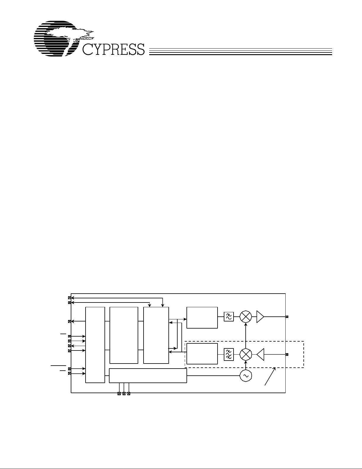
2.0 Functional Description
The CYWUSB6932/CYWUSB6934 Integrated Circuits (ICs)
are highly integrated 2.4 GHz Direct Sequence Spread
Spectrum (DSSS) Radio System-on-Chip (SoC) ICs. From the
Serial Peripheral Interf ace (SPI) to the an tenna, these IC s are
single-chi p 2.4 GHz D SSS G aus sian Freq uen cy S hift K eying
(GFSK) baseband modems that connect directly to a USB
controller or a standard microcontroller as shown in
Figure 3-1.
The CYWUSB6932 is a transmit-only IC and is available in a
cost saving 28 -pin SOIC package. The CYWUSB6934 is a
transceiver IC and is offered in both a 28-pin SOIC package
and a small fo otprint 48-pin QFN package .
3.0 Applications
• PC Human Interface Devices (HID)
• Mice
• Keyboards
• Joysticks
• Peripheral Gaming Devices
• Game Controllers
• Con so le Key boa rds
• General
• Pre senter Tools
• Remote Controls
• Consumer Electronics
• Barcode Scanners
• POS Peripherals
• Toys
DIOVAL
DIO
GFSK
Modulator
GFSK
Demodulator
RFOUT
RFIN
CYWUSB6934 Only
IRQ
SS
SCK
MISO
MOSI
RESET
PD
Digital
SERDES
A
SERDES
B
X13
X13IN
DSSS
Baseband
A
DSSS
Baseband
B
Synthesizer
X13OUT
Figure 3-1. CYWUSB6932/CYWUSB6934 Simplified Block Diagram
Cypress Semiconductor Corporation • 3901 North First Street • San Jose, CA 95134 • 408-943-2600
Document 38-16007 Rev. *F Revised August 6, 2004

CYWUSB6932
CYWUSB6934
3.1 Applications Support
The CYWUSB6932/CYWUSB6934 ICs are supported by the
CY3632 WirelessUSB Development Kit. The development kit
provides all of the materi als an d docum ent s nee ded to c ut the
cord on wired applications including two radio modules that
connect directly to two prototyping platform boards, comprehensive WirelessUSB protoc ol code examples a WirelessUS B
Listener tool and all o f the a ssociat ed sc hemat ics, g erber fi les
and bill of materials.
The CY4632 WirelessUSB LS Keyboard Mouse Reference
Design provides a production-worthy example of a wireless
mouse and keyboard system.
The CY3633 WirelessUSB LS Gaming Development Kit
provides support for designing a wireless gamepad for the
major gaming consoles and is offered as an accessory to the
CY3632 WirelessUSB.
4.0 Functional Overview
The CYWUSB6932/CYWUSB6934 ICs provide a complete
WirelessUS B LS SPI to antenn a radio modem. Th e SoC is
designed to implement wireless devices operating in the
worldwide 2.4 GHz Industrial, Scientific, and Medical (ISM)
frequency band (2.400 GHz - 2.4835 GHz). It is intended for
systems compliant with world-wide regulations covered by
ETSI EN 301 489-1 V1.4.1, ETSI EN 300 328-1 V1.3.1
(European Countries); FCC CFR 47 Part 15 (USA and
Industry Canada) and ARIB STD-T66 (Japan).
The CYWUSB6934 IC cont ain s a 2.4 GHz ra dio transc eiver, a
GFSK modem and a dual DSSS reconfigurable baseband.
The CYWUSB6932 IC conta ins a 2.4 G Hz radio tra nsmit-on ly,
a GFSK modem and a DSSS baseband. The radio and
baseband are both code- and frequency-agile. Forty-nine
spreading codes selected for optimal performance (Gold
codes) are supported across 78 1 MHz channels yielding a
theoretical spectral capacity of 3822 channels. Both ICs
support a range of up to 10 meters or more.
4.1 2.4 GHz Radio
The receiver and trans mitter are a single-conve rsion low-Intermediate Frequency (low-IF) architecture with fully integrated
IF channel matched filters to achieve high performance in the
presence of interference. An integrated Power Amplifier (PA)
provides an output power control range of 30 dB in seven
steps.
Both the receiver and transmitter integrated Voltage
Controlled Oscillator (VCO) and synthes izer have the ag ility to
cover the complete 2. 4 GHz GFSK radio transmitte r ISM band.
The VCO loop filter is also integrated on-chip.
4.2 GFSK Modem
The transmitter uses a DSP-based vector modulator to
convert the 1 MHz chips to an accurate GFSK carrier.
The receiver uses a fully integrated Freq uency Modulator (FM )
detector with automatic data slicer to demodulate the GFSK
signal.
4.3 Dual DSSS Baseband
Data is converted to DSSS chips by a digital spreader.
De-spreading is p erformed by an oversam pled correlat or . Th e
DSSS baseband cancels spurious noise and assembles
properly correlated data bytes.
The DSSS baseband has four operating modes: 64 chips/bit
Single Channel, 32 chip s/bit Dual Channe l, 32 chi ps/bi t Single
Channel 2x Oversampled, and 32 chips/bit Single Channel
Dual Data Rate (DDR).
4.3.1 64 chips/bit Single Channel
The baseband supports a single data stream operating at
15.625 kbits/sec. The advantage of selecting this mode is its
ability to tolerate a noisy environment. This is because the
15.625 kbits/sec data stream utilizes the longest PN Code
resulting in the high es t p r oba bil ity for recovering packe t s ov er
the air. This mode can also be selected for systems requiring
data transmissi ons over lon ger ranges.
4.3.2 32 chips/bit Dual Channel
The baseband supports two non-simultaneous data streams
each operating at 31.25 kbits/sec.
4.3.3 32 chips/bit Single Channel 2x Oversampled
The baseband supports a single data stream operating at
31.25 kbits/sec that is sampled twice as much as the other
modes. The advantage of selecting this mode is its ability to
tolerate a noisy environment.
4.3.4 32 chips/bit Single Channel Dual Data Rate (DDR)
The baseband spread s bits in p airs and s upports a si ngle data
stream operating at 62.5 kbits/sec.
4.4 Serializer/Deserializer (SERDES)
Both ICs provide a data Serializer/Deserializer (SERDES),
which provides byte-l evel framing of transmi t and receive dat a.
Bytes for transmission are loaded into the SERDES and
receive bytes are read from the SERDES via the SPI in terface.
The SERDES provides double buffering of transmit and
receive data. While one byte is being transmitted by the radio
the next byte can be written to the SERDES data register
insuring there are no breaks in transmitted data.
After a receive byte has been received it is loaded into the
SERDES data register and can be read at any time until the
byte is received, at which time the old contents of the
next
SERDES data register wil l be overwritten.
4.5 Application Interfaces
Both ICs have a fully synchronous SPI slave interface for
connectivity to the application MCU. Configuration and
byte-oriented data transfer can be performed over this
interface. An interrupt is provided to trigger real time events.
An optional SERDES Bypas s mode (DIO) is provided for a pplications that require a synchronous serial bit-oriented data
path. This interface is for data only.
4.6 Clocking and Power Management
A 13 MHz crystal (±50 ppm or better) is directly connected to
X13IN and X13 without the need for ex ter nal capacitors. Both
ICs have a programmable trim capability for adjusting the
on-chip load capacitance supplied to the crystal. The Radio
Frequency (RF) circuitry has on-chip decoupling capacitors.
Document 38-16007 Rev. *F Page 2 of 33

CYWUSB6932
CYWUSB6934
Both devices are po wered from a 2.7V to 3.6V DC s upply . Both
devices can be shutdown to a fully static state using the PD
pin.
Below are the requirements for the crystal to be directly
connected to X13IN and X13:
• Nominal Frequency: 13 MHz
• Operating Mode: Fundam ental Mode
• Resonance Mode: Paral le l Reson ant
• Frequency Stability :
• Series Resistanc e: ≤ 100 ohms
• Load Capacitance: 10 pF
• Drive Level: 10 uW–100 uW
± 50 ppm
4.7 Receive Signal Strength Indicator (RSSI)
The RSSI register (Reg 0x22) returns the relative signal
strength of the ON-channel signal power and can be used to:
1) determine the connec tio n qu ali ty, 2) determine the value of
the noise floor, and 3) check for a quiet channel before transmitting.
The internal RSSI voltage is sampled through a 5-bit
analog-to-digital converter (ADC). A state machine controls
the conversion process. Under normal conditions, the RSSI
state machine initiates a conversion when an ON-channel
carrier is detected and remains above the noise floor for over
50uS. The conversion produces a 5-bit value in the RSSI
register (Reg 0x22, bits 4:0) along with a valid bit, RSSI
register (Reg 0x22, bit 5). The state machine then remains in
HALT mode and does not reset for a new conversion until the
receive mode is toggled off and on. Once a connection has
been established, the RSSI register can be read to determine
the relative connec ti on quality of the ch ann el. A R SSI reg is ter
value lower than 10 indi cates that the receive d signal str ength
is low, a value greater than 28 indicates a strong signal level.
To check for a quiet channel before transmitting, first set up
receive mode properl y and read the RSSI register (Reg 0 x22).
If the valid bit is zero, then force the Carrier Detect register
(Reg 0x2F, bit 7=1) to initiate an ADC conversion. Then, wait
greater than 50uS and read the RSSI register again. Next,
clear the Carrier Detect Register (Reg 0x2F, bit 7=0) and turn
the receiver OFF. Measuring the noise floor of a quiet channe l
is inherently a 'noisy' process so, for best results, this
procedure should be repeated several times (~20) to compute
an average no ise floor level. A RSSI re gister value of 0-10
indicates a channel that is relatively quiet. A RSSI register
value greater than 10 indicates the channel is probably being
used. A RSSI register value greater than 28 indicates the
presence of a strong signal.
5.0 Application Interfaces
5.1 SPI Interface
The CYWUSB6932/CYWUSB6934 ICs have a four-wire SPI
communication interface between an application MCU and
one or more slave devices. The SPI interface supports
single-byte and multi-byte serial transfers. The four-wire SPI
communications interface consists of Master Out-Slave In
(MOSI), Master In-Slave Out (MISO), Serial Clock (SCK), and
Slave Select (SS
The SPI receives SCK from an application MCU on the SCK
pin. Data from the application MCU is shifted in on the MOSI
pin. Data to the application MCU is shifted out on the MISO
pin. The active-low Slave Selec t (SS)
initiate a SPI transfer.
The application MCU can initiate a SPI data transfer via a
multi-byte transact ion. T he first byt e is the Command/Add ress
byte, and the following bytes are the data bytes as shown in
Figure 5-1 through Figure 5-4. The SS
deasserted between bytes. The SPI communications is as
follows:
• Command Direct ion (b it 7) = “0” En ables SPI rea d tran saction. A “1” enables SPI write transactions.
• Command Incremen t (bit 6) = “1” Enables SPI auto address
increment. When se t, the addres s field automa tically i ncrements at the en d of each data byte in a bur s t access, ot herwise the same address is accessed.
• Six bits of address.
• Eight bits of data.
The SPI communications interface has a burst mechanism,
where the command byte can be followed by as many data
bytes as desired. A burst transaction is terminated by
deasserting the slave select (SS
The SPI communications i nter fac e s ing le re ad a nd b urs t rea d
sequences are shown in Figure 5-2 and Figure 5-3, respectively.
The SPI communication s interfac e single write and burs t write
sequences are shown in Figure 5-4 and Figure 5-5, respectively.
).
pin must be asserted to
signal should not be
= 1).
Document 38-16007 Rev. *F Page 3 of 33
CYWUSB6932
CYWUSB6934
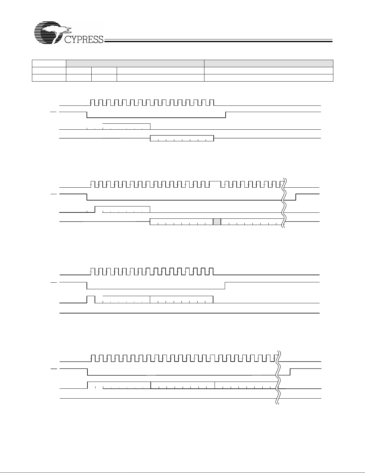
Figure 5-1. SPI Transaction Format
Byte 1 Byte 1+N
Bit # 7 6 [5:0] [7:0]
Bit Name DIR INC Address Data
SCK
SS
addrcm d
A0A1A2A3A4A5
MOSI
DIR INC
00
data to mcu
MISO
D6D7
D0D1D2D3D4D5
Figure 5-2. SPI Single Read Sequence
SCK
SS
MOSI
MISO
DIR INC
01
addrcm d
A0A1A2A3A4A5
da ta to mcu
D6D7
1
D0D1D2D3D4D5
data to mcu
D6D7
1+N
D0D1D2D3D4D5
SCK
SS
MOSI
MISO
SCK
SS
MOSI
MISO
DIR INC
10
DIR INC
11
Figure 5-3. SPI Burst Read Sequence
addrcmd
D6D7
A0A1A2A3A4A5
data fro m mcu
Figure 5-4. SPI Single Write Sequence
addrcm d
da ta fro m mcu
D6D7
A0A1A2A3A4A5
Figure 5-5. SPI Burst Write Sequence
D0D1D2D3D4D5
1
data from mcu
D0D1D2D3D4D5
D6D7
1+N
D0D1D2D3D4D5
Document 38-16007 Rev. *F Page 4 of 33
CYWUSB6932
CYWUSB6934
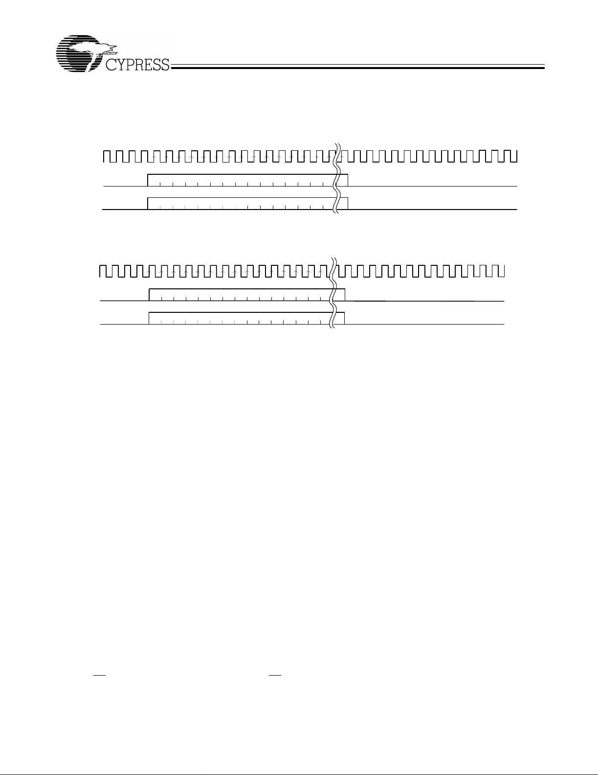
5.2 DIO Interface
The DIO communications interface is an optional SERDES
bypass data-only transfer interface. In receive mode, DIO and
DIOVAL are valid after the falling edge of IRQ, which clocks
IRQ
DIOVAL
v7v6v5v4v3v2
v9v8v1v0
data to mcu
DIO
d1d0
d7d6d5d4d3d2
Figure 5-6. DIO Receive Sequence
IRQ
DIOVAL
v1v0
v9v8
v7v6v5v4v3v2
data from mcu
DIO
d1d0
d7d6d5d4d3d2
Figure 5-7. DIO Transmit Sequence
the data as shown in
Figure 5-6. In transmit mode, DIO and
DIOVAL are sampled on the falling edge of the IRQ, which
clocks the data as shown in
Figure 5-7. The application MCU
samples the DIO and DIOVAL on the rising edge of IRQ.
v...v14v1 3v12v11v10
d...d14d13d12d11d1 0d9d8
v...v1 4v13v12v11v10
d...d1 4d13d12d11d10d9d8
5.3 Interrupts
The CYWUSB6932/CYWUSB6934 ICs feature three sets of
interrupts: transmit, received (CYWUSB6932 only), and a
wake interrupt. These interrupts all share a single pin (IRQ),
but can be independ ently enab led/disa bled. In tran smit mod e,
all receive interru pts are automa tically disab led, and in receive
mode all transmit interrupts are automatically disabled.
However, the contents of the enable registers are preserved
when switching between tran sm it and receiv e mod es .
Interrupts are ena bled and the st atus read thr ough 6 registers:
Receive Interrupt Enable (Reg 0x07), Recei ve Interrupt S t atus
(Reg 0x08), Transmit Interrupt Enable (Reg 0x0D), Transmit
Interrupt Status (Reg 0x0E), Wake Enable (Reg 0x1C), Wake
Status (Reg 0x1D).
If more than 1 interrupt is enabled at any time, it is necessary
to read the relevant interrupt st atus register to determine which
event caused the IRQ pin to assert. Even when a given
interrupt source is disabled, the status of the condition that
would otherwise cause an interrupt can be determined by
reading the appropriate int errupt st atus regis ter. It is therefore
possible to use th e devic es with out mak ing us e of the I RQ pin
at all. Firmware can poll the interrupt status register(s) to wait
for an event, rather than using the IRQ pin.
The polarity of all interrupt s can be s et by writing to the Co nfiguration register (Reg 0x05), and it is possible to configure the
IRQ pin to be o pen drain (if a ctive low) o r open source (if active
high).
5.3.1 Wake Interrupt
When the PD pin is low, the oscillator is stopped. After PD is
deasserted, the oscillator takes time to start, and until it has
done so, it is not safe to use the SPI interface. The wake
interrupt indicates that the oscillator has started, and that the
device is ready to receive SPI transfers.
The wake interrupt is enabled by setting bit 0 of the Wake
Enable register (Reg 0x1C, bit 0=1). Whether or not a wake
interrupt is pendin g is indicated by the state of bit 0 of the Wake
Status register (Reg 0x1D, bit 0). Reading the Wake Status
register (Reg 0x1D) clears the interrupt.
5.3.2 Transmit Interrupts
Four interrupts a re p rov id ed t o fl ag the oc cu rren ce of t rans m it
events. The interrupts are enabled by writing to the Transmit
Interrupt Enable register (Reg 0x0D), and their status may be
determined by reading the Transmit Interrupt Status register
(Reg 0x0E). If more than 1 interrupt i s enabled , it is neces sary
to read the Transmit Interrupt Status register (Reg 0x0E) to
determine which event caused the IRQ pin to assert.
The function and operatio n of these interrupts are des cribed in
detail in
Section 7.0.
5.3.3 Receive Interrupts
Eight interrupts are provided to flag the occurrence of receive
events, four each fo r SERDES A and B. In 64 c hips /bit and 3 2
chips/bit DDR modes, only the SERDES A interrupts are
available, and the SERDES B interrupts will never trigger,
even if enabled. The interrupts are enabled by writing to the
Receive Interrupt Enab le regis ter (Reg 0x 07), and their st atu s
may be determin ed by reading the Rece ive Interrupt Status
register (Reg 0x08 ). If m ore th an on e int errup t i s en abl ed, it i s
necessary to read the Receive Interrupt Status register (Reg
0x08) to determine whic h e ven t ca us ed th e IRQ pin to as se rt.
The function and operatio n of these interrupts are des cribed in
detail in
Section 7.0.
Document 38-16007 Rev. *F Page 5 of 33
6.0 Application Examples
CYWUSB6932
CYWUSB6934
Battery
Optical
Mouse
Sensor
Buttons
LDO/
DC2DC
+
-
Vcc
3.3 V
RESET
Vcc
0.1µF
10pF
PCB Trace
Inverted “F”
Antenna
(PIFA)
RFOUT
PD
Application MCU
IRQ
SPI
WUSB LS
13MHz
Crystal
4
Figure 6-1. CYWUSB6932 Transmit-Only Battery-Powered Device
1.2 pF
PCB Tr ace
Inverted “F”
Antenna
(PIFA)
3.0 pF
3.3 nH
0.1 µF
3.6 pF
1.0 pF
13MHz
Cry stal
3.3V
1µF
RFOUT
RFIN
W irelessUSB L S
LDO
RESET
PD
IRQ
2.2K
2.2K
MISO
SS
0.1µF 4.7µF
SCK
MOSI
Figure 6-2. CYWUSB6934 USB Bridge Transceiver
5V
Vcc
Cypr ess
enCoRe
USB MCU
USB I/F
1.3K
D+/D-
2
Document 38-16007 Rev. *F Page 6 of 33

CYWUSB6932
CYWUSB6934
7.0 Register Descriptions
through the SPI interface. All registers are read and writable,
except where noted.
Table 7-1 displays the list of registers inside the
CYWUSB6932/CYWUSB6934 ICs that are addressable
Table 7-1. CYWUSB6932/CyWUSB6934 Register Map
[2]
CYWUSB6934
Register Name Mnemonic
Address Page Default Access
Revision ID REG_ID 0x00 8 0x07 RO
Synthesizer A Counter REG_SYN_A_CNT 0x01 8 0x00 RW
Synthesizer N Counter REG_SYN_N_CNT 0x02 8 0x00 RW
Control REG_CONTROL 0x03 9 0x00 RW
Data Rate REG_DATA_RATE 0x04 10 0x00 RW
Configuration REG_CONFIG 0x05 10 0x01 RW
SERDES Control REG_SERDES_CTL 0x06 11 0x03 RW
Receive Interrupt Enable REG_RX_INT_EN 0x07
Receive Interrupt Status REG_RX_INT_STAT 0x08
Receive Data A REG_RX_DATA_A 0x09
Receive Valid A REG_RX_VALID_A 0x0A
Receive Data B REG_RX_DATA_B 0x0B
Receive Valid B REG_RX_VALID_B 0x0C
[1]
[1]
[1]
[1]
[1]
[1]
12 0x00 RW
13 0x00 RO
14 0x00 RO
14 0x00 RO
14 0x00 RO
14 0x00 RO
Transmit Interrupt Enable REG_TX_INT_EN 0x0D 15 0x00 RW
Transmit Interrupt Status REG_TX_INT_STAT 0x0E 16 0x00 RO
Transmit Data REG_TX_DATA 0x0F 17 0x00 RW
Transmit Valid REG_TX_VALID 0x10 17 0x00 RW
PN Code REG_PN_CODE 0x11–0x18 17
Threshold Low REG_THRESHOLD_L 0x19
Threshold High REG_THRESHOLD_H 0x1A
[1]
[1]
0x1E8B6A3DE0E9B222 RW
18 0x08 RW
18 0x38 RW
Wake Enable REG_WAKE_EN 0x1C 18 0x00 RW
Wake Status REG_WAKE_STAT 0x1D 19 0x01 RO
Analog Control REG_ANALOG_CTL 0x20 19 0x04 RW
Channel REG_CHANNEL 0x21 20 0x00 RW
Receive Signal Strength Indicator REG_RSSI 0x22
[1]
20 0x00 RO
Power Control REG_PA 0x23 20 0x00 RW
Crystal Adjust REG_CRYSTAL_ADJ 0x24 21 0x00 RW
VCO Calibration REG_VCO_CAL 0x26 21 0x00 RW
AGC Control REG_AGC_CTL 0x2E 21 0x00 RW
Carrier Detect REG_CARRIER_DETECT 0x2F 21 0x00 RW
Clock Manual REG_CLOCK_MANUAL 0x32 22 0x00 RW
Clock Enable REG_CLOCK_ENABLE 0x33 22 0x00 RW
Synthesizer Lock Count REG_SYN_LOCK_CNT 0x38 22 0x64 RW
Manufacturing ID REG_MID 0x3C–0x3F 22 – RO
Notes:
1. Register not applicable to CYWUSB6932.
2. All registers are accessed Little Endian.
Document 38-16007 Rev. *F Page 7 of 33
CYWUSB6932
CYWUSB6934
Figure 7-1. Revision ID Register
Addr: 0x00 REG_ID Default: 0x07
76543210
Silicon ID Product ID
Bit Name Description
7:4 Silicon ID
3:0 Product ID These are the Product ID revision bits. Fixed at value 0111. These bits are read-only.
These are the Silicon ID revision bits. 0000 = Rev A, 0001 = Rev B, etc. These bits are read-only.
Figure 7-2. Synthesizer A Counter
Addr: 0x01 REG_SYN_A_CNT Default: 0x00
76543210
Reserved Count
Bit Name Description
7:5 Reserved These bits are reserved and should be written with zeros.
4:0 Count The Synthesizer A Counter register is used for diagnostic purposes and is not recommended for normal operation. The
Channel register is the recommended method of setting the Synthesizer frequency.
The Synthesizer A Count along with the Synthesizer N Count can be used to generate the Synthesizer frequency. The
range of valid values of the Synthesizer A Count is 0 through 31. Using the Synthesizer A and N Count register is an
alternative to using the Channel register. Selection between the use of the Channel register or the A and N registers is
done through the Channel register (Reg 0x21, bit 7). When in Channel mode the A and N Count bits can be used to read
the A and N values derived directly from the Channel.
Figure 7-3. Synthesizer N Counter
Addr: 0x02 REG_SYN_N_CNT Default: 0x00
76543210
Reserved Count
Bit Name Description
7 Reserved This bit is reserved and should be written with zero.
6:0 Count The Synthesizer N Counter register is used for diagnostic purposes and therefore is not recommended for normal
operation. The Channel register is the recommended method of setting the Synthesizer frequency.
The Synthesizer N Count along with the Synthesizer A Count can be used to generate the Synthesizer frequency. The
range of valid values of the Synthesizer N Count is 74 through 76. Using the Synthesizer A and N Count register is an
alternative to using the Channel register. Selection between the use of the Channel register or the A and N registers is
done through the Channel register (Reg 0x21, bit 7). When in Channel mode the A and N Count bits can be used to read
the A and N values derived directly from the Channel.
Document 38-16007 Rev. *F Page 8 of 33

CYWUSB6932
CYWUSB6934
Figure 7-4. Control
Addr: 0x03 REG_CONTROL Default: 0x00
76543210
RX
Enable
Bit Name Description
7 RX Enable The Receive Enable bit is used to place the IC in receive mode.
6 TX Enable The Transmit Enable bit is used to place the IC in transmit mode.
5 PN Code Select The Pseudo-Noise Code Select bit selects between the upper or lower half of the 64 chips/bit PN code.
4 Auto Syn Count
Select
3 Auto PA Disable The Auto Power Amplifier Disable bit is used to determine the method of controlling the Power Amplifier. The two options
2 PA Enable The PA Enable bit is used to enable or disable the Power Amplifier.
1 Auto Syn
Disable
0 Syn Enable The Synthesizer Enable bit is used to enable or disable the Synthesizer.
TX
Enable
1 = Receive Enabled
0 = Receive Disabled
1 = Transmit Enabled
0 = Transmit Disabled
1 = 32 Most Significant Bits of PN code are used
0 = 32 Least Significant Bits of PN code are used
This bit applies only when the Code Width bit is set to 32 chips/bit PN codes (Reg 0x04, bit 2=1).
The Auto Synthesizer Count Select bit is used to select the method of determining the settle time of the synthesizer. The
two options are a programmable settle time based on the value in Syn Lock Count register (Reg 0x38), in units of 2 us,
or by the auto detection of the synthesizer lock.
1 = Synthesizer settle time is based on a count in Syn Lock Count register (Reg 0x38)
0 = Synthesizer settle time is based on the internal synthesizer lock signal
It is recommended that the Auto Syn Count Select bit is set to 1 as that guarantees a consistent settle time for the
synthesizer.
are automatic control by the baseband or by firmware through register writes.
1 = Register controlled PA Enable.
0 = Auto PA Enable.
When this bit is set to 1 the state of PA enable is directly controlled by bit PA Enable (Reg 0x03, bit 2). It is recommended
that this bit is set to 0 leaving
1 = Power Amplifier Enabled
0 = Power Amplifier Disabled
This bit only applies when the Auto PA Disable bit is selected (Reg 0x03, bit 3=1), otherwise this bit is don’t care.
The Auto Synthesizer Disable bit is used to determine the method of controlling the Synthesizer. The two options are
automatic control by the baseband or by firmware through register writes.
1 = Register controlled Synthesizer Enable.
0 = Auto Synthesizer Enable.
When this bit is set to 1 the state of the Synthesizer is directly controlled by bit Syn Enable (Reg 0x03, bit 0). When this
bit is set to 0 the state of the Synthesizer is controlled by the Auto Syn Count Select bit (Reg 0x03, bit 4). It is recommended that this bit is set to 0 leaving the Synthesizer control to the baseband.
1 = Synthesizer Enabled
0 = Synthesizer Disabled
This bit only applies when Auto Syn Disable bit is selected (Reg 0x03, bit 1=1), otherwise this bit is don’t care.
PN Code
Select
Auto Syn
Count Select
Auto PA
Disable
the PA control to the baseband.
PA Enable Auto Syn
Disable
Syn Enable
Document 38-16007 Rev. *F Page 9 of 33

CYWUSB6932
CYWUSB6934
Figure 7-5. Data Rate
Addr: 0x04 REG_DATA_RATE Default: 0x00
76543210
Reserved Code Width Data Rate Sample Rate
Bit Name Description
7:3 Reserved
[3]
Code Width The Code Width bit is used to select between 32 chips/bit and 64 chips/bit PN codes.
2
[3]
Data Rate The Data Rate bit allows the user to select Double Data Rate mode of operation which delivers a raw data rate of
1
[3]
Sample
0
Rate
These bits are reserved and should be written with zeros.
1 = 32 chips/bit PN codes
0 = 64 chips/bit PN codes
The number of chips/bit used impacts a number of factors such as data throughput, range and robustness to interference.
By choosing a 32 chips/bit PN-code, the data throughput can be doubled or even quadrupled (when double data rate is
set). A 64 chips/bit PN code offers improved range over its 32 chips/bit counterpart as well as more robustness to
interference. By selecting to use a 32 chips/bit PN code a number of other register bits are impacted and need to be
addressed. These are PN Code Select (Reg 0x03, bit 5), Data Rate (Reg 0x04, bit 1), and Sample Rate (Reg 0x04, bit 0).
62.5kbits/sec.
1 = Double Data Rate - 2 bits per PN code (No odd bit transmissions)
0 = Normal Data Rate - 1 bit per PN code
This bit is applicable only when using 32 chips/bit PN codes which can be selected by setting the Code Width bit (Reg
0x04, bit 2=1). When using Double Data Rate, the raw data throughput is 62.5 kbits/sec because every 32 chips/bit PN
code is interpreted as 2 bits of data. When using this mode a single 64 chips/bit PN code is placed in the PN code register.
This 64 chips/bit PN code is then split into two and used by the baseband to offer the Double Data Rate capability.
using Normal Data Rate, the raw data throughput is 32kbits/sec.
potentially correlate data using two differing 32 chips/bit PN codes.
The Sample Rate bit allows the use of the 12x sampling when using 32 chips/bit PN codes and Normal Data Rate.
1 = 12x Oversampling
0 = 6x Oversampling
Using 12x oversampling improves the correlators receive sensitivity. When using 64 chips/bit PN codes or Double Data
Rate this bit is don’t care. When in the Normal Data Rate setting and choosing 12x oversampling, eliminates the ability to
receive from two different PN codes. Therefore the only time when 12x oversampling is to be selected is when a 32 chips/bit
PN code is being used and there is no need to receive data from sources with two different PN codes.
Additionally , Normal Data Rate enables the user to
When
Figure 7-6. Configuration
Addr: 0x05 REG_CONFIG Default: 0x01
76543210
Reserved Receive Invert Transmit Invert Reserved IRQ Pin Select
Bit Name Description
7:5 Reserved These bits are reserved and should be written with zeros.
4 Receive Invert The Receive Invert bit is used to invert the received data.
3 Transmit Invert The Transmit Invert bit is used to invert the data that is to be transmitted.
2 Reserved This bit is reserved and should be written with zero.
1:0 IRQ Pin Select The Interrupt Request Pin Select bits are used to determine the drive method of the IRQ pin.
Note:
3. The followin g Reg 0x04, bits 2:0 values are not valid:
• 001 - Not Valid
• 010 - Not Valid
• 011 - Not Valid
• 111 - Not Valid
1 = Inverted over-the-air Receive data
0 = Non-inverted over-the-air Receive data
1 = Inverted Transmit Data.
0 = Non-inverted Transmit Data.
11 = Open Source (asserted = 1, deasserted = Hi-Z)
10 = Open Drain (asserted = 0, deasserted = Hi-Z)
01 = CMOS (asserted = 1, deasserted = 0)
00 = CMOS Inverted (asserted = 0, deasserted = 1)
Document 38-16007 Rev. *F Page 10 of 33

CYWUSB6932
CYWUSB6934
Figure 7-7. SERDES Control
Addr: 0x06 REG_SERDES_CTL Default: 0x03
76543210
Reserved SERDES
Bit Name Description
7:4 Reserved These bits are reserved and should be written with zeros.
3 SERDES Enable The SERDES Enable bit is used to switch between bit-serial mode and SERDES mode.
2:0 EOF Length The End of Frame Length bits are used to set the number of sequential bit times for an inter-frame gap without valid
1 = SERDES enabled.
0 = SERDES disabled, bit-serial mode enabled.
When the SERDES is enabled data can be written to and read from the IC one byte at a time, through the use of the
SERDES Data registers. The bit-serial mode requires bits to be written one bit at a time through the use of the
DIO/DIOVAL pins, refer to section 3.2. It is recommended that SERDES mode be used to avoid the need to manage
the timing required by the bit-serial mode.
data before an EOF event will be generated. When in receive mode and a valid bit has been received the EOF event
can then be identified by the number of bit times that expire without correlating any new dat a. The EOF event causes
data to be moved to the proper SERDES Data Register and can also be used to generate interrupts. If 0 is the EOF
length, an EOF condition will occur at the first invalid bit after a valid reception.
Enable
EOF Length
Document 38-16007 Rev. *F Page 11 of 33

CYWUSB6932
CYWUSB6934
Figure 7-8. Receive Interrupt Enable
Addr: 0x07 REG_RX_INT_EN Default: 0x00
76543210
Underflow B Overflow B EOF B Full B Underflow A Overflow A EOF A Full A
Bit Name Description
7 Underflow B The Underflow B bit is used to enable the interrupt associated with an underflow condition with the Receive SERDES
6 Overflow B The Overflow B bit is used to enable the interrupt associated with an overflow condition with the Receive SERDES Data
5 EOF B The End of Frame B bit is used to enable the interrupt associated with the Channel B Receiver EOF condition.
4 Full B The Full B bit is used to enable the interrupt associated with the Receive SERDES Data B register (Reg 0x0B) having
3 Underflow A The Underflow A bit is used to enable the interrupt associated with an underflow condition with the Receive SERDES
2 Overflow A The Overflow A bit is used to enable the interrupt associated with an overflow condition with the Receive SERDES Data
1 EOF A The End of Frame A bit is used to enable the interrupt associated with an End of Frame condition with the Channel A
0 Full A The Full A bit is used to enable the interrupt associated with the Receive SERDES Data A register (0x09) having data
Data B register (Reg 0x0B)
1 = Underflow B interrupt enabled for Receive SERDES Data B
0 = Underflow B interrupt disabled for Receive SERDES Data B
An underflow condition occurs when attempting to read the Receive SERDES Data B register (Reg 0x0B) when it is
empty.
B register (Reg 0x0B)
1 = Overflow B interrupt enabled for Receive SERDES Data B
0 = Overflow B interrupt disabled for Receive SERDES Data B
An overflow condition occurs when new received data is written into the Receive SERDES Data B register (Reg 0x0B)
before the prior data is read out.
1 = EOF B interrupt enabled for Channel B Receiver.
0 = EOF B interrupt disabled for Channel B Receiver.
The EOF IRQ asserts during an End of Frame condition. End of Frame conditions occur after at least one bit has been
detected, and then the number of invalid bits in the frame exceeds the number in the EOF length field. If 0 is the EOF
length, and EOF condition will occur at the first invalid bit after a valid reception. This IRQ is cleared by reading the
receive status register
data placed in it.
1 = Full B interrupt enabled for Receive SERDES Data B
0 = Full B interrupt disabled for Receive SERDES Data B
A Full B condition occurs when data is transferred from the Channel B Receiver into the Receive SERDES Data B
register (Reg 0x0B). This could occur when a complete byte is received or when an EOF event occurs whether or not
a complete byte has been received.
Data A register (Reg 0x09)
1 = Underflow A interrupt enabled for Receive SERDES Data A
0 = Underflow A interrupt disabled for Receive SERDES Data A
An underflow condition occurs when attempting to read the Receive SERDES Data A register (Reg 0x09) when it is
empty.
A register (0x09)
1 = Overflow A interrupt enabled for Receive SERDES Data A
0 = Overflow A interrupt disabled for Receive SERDES Data A
An overflow condition occurs when new receive data is written into the Receive SERDES Data A register (Reg 0x09)
before the prior data is read out.
Receiver.
1 = EOF A interrupt enabled for Channel A Receiver.
0 = EOF A interrupt disabled for Channel A Receiver.
The EOF IRQ asserts during an End of Frame condition. End of Frame conditions occur after at least one bit has been
detected, and then the number of invalid bits in a frame exceeds the number in the EOF length field. If 0 is the EOF
length, an EOF condition will occur at the first i nvalid bit after a valid reception. This IRQ is cleared by reading the receive
status register.
written into it.
1 = Full A interrupt enabled for Receive SERDES Data A
0 = Full A interrupt disabled for Receive SERDES Data A
A Full A condition occurs when data is transferred from the Channel A Receiver into the Receive SERDES Data A
register (Reg 0x09). This could occur when a complete byte is received or when an EOF event occurs whether or not
a complete byte has been received.
Document 38-16007 Rev. *F Page 12 of 33

CYWUSB6932
CYWUSB6934
Figure 7-9. Receive Interrupt Status
Addr: 0x08 REG_RX_INT_STAT Default: 0x00
76543210
Valid B Flow Violation
Bit Name Description
7 Valid B The Valid B bit is true when all the bits in the Receive SERDES Data B register (Reg 0x0B) are valid.
6 Flow Violation BThe Flow Violation B bit is used to signal whether an overflow or underflow condition has occurred for the Receive
5 EOF B The End of Frame B bit is used to signal whether an EOF event has occurred on the Channel B receive.
4 Full B The Full B bit is used to signal when the Receive SERDES Data B register (Reg 0x0B) is filled with data.
3 Valid A The Valid A bit is true when all of the bits in the Receive SERDES Data A Register (Reg 0x09) are valid.
2 Flow Violation AThe Flow Violation A bit is used to signal whether an overflow or underflow condition has occurred for the Receive
1 EOF A The End of Frame A bit is used to signal whether an EOF event has occurred on the Channel A receive.
0 Full A The Full A bit is used to signal when the Receive SERDES Data A register (Reg 0x09) is filled with data.
B
1 = All bits are valid for Receive SERDES Data B.
0 = Not all bits are valid for Receive SERDES Data B.
When data is written into the Receive SERDES Data B register (Reg 0x0B) this bit is set if all of the bits within the byte
that has been written are valid. This bit cannot generate an interrupt.
SERDES Data B register (Reg 0x0B).
1 = Overflow/underflow interrupt pending for Receive SERDES Data B.
0 = No overflow/underflow interrupt pending for Receive SERDES Data B.
Overflow conditions occur when the radio loads new data into the Receive SERDES Data B register (Reg 0x0B) before
the prior data has been read. Underflow conditions occur when trying to read the Receive SERDES Data B register
(Reg 0x0B) when the register is
1 = EOF interrupt pending for Channel B.
0 = No EOF interrupt pending for Channel B.
An EOF condition occurs for the Channel B Receiver when receive has begun and then the number of bit times
specified in the SERDES Control register (Reg 0x06) elapse without any valid bits being received. This bit is cleared
by reading the Receive Interrupt Status register (Reg 0x08)
1 = Receive SERDES Data B full interrupt pending.
0 = No Receive SERDES Data B full interrupt pending.
A Full B condition occurs when data is transferred from the Channel B Receiver into the Receive SERDES Data B
register (Reg 0x0B). This could occur when a complete byte is received or when an EOF event occurs whether or not
a complete byte has been received.
1 = All bits are valid for Receive SERDES Data A.
0 = Not all bits are valid for Receive SERDES Data A.
When data is written into the Receive SERDES Data A register (Reg 0x09) this bit is set if all of the bits within the byte
that has been written are valid. This bit cannot generate an interrupt.
SERDES Data A register (Reg 0x09).
1 = Overflow/underflow interrupt pending for Receive SERDES Data A.
0 = No overflow/underflow interrupt pending for Receive SERDES Data A.
Overflow conditions occur when the radio loads new data into the Receive SERDES Data A register (Reg 0x09) before
the prior data has been read. Underflow conditions occur when trying to read the Receive SERDES Data A register
(Reg 0x09) when the register is empty. This bit is cleared by reading the Receive Interrupt Status register (Reg 0x08)
1 = EOF interrupt pending for Channel A.
0 = No EOF interrupt pending for Channel A.
An EOF condition occurs for the Channel A Receiver when receive has begun and then the number of bit times
specified in the SERDES Control register (0x06) elapse without any valid bits being received. This bit is cleared by
reading the Receive Interrupt Status register (Reg 0x08).
1 = Receive SERDES Data A full interrupt pending.
0 = No Receive SERDES Data A full interrupt pending.
A Full A condition occurs when data is transferred from the Channel A Receiver into the Receive SERDES Data A
Register (Reg 0x09). This could occur when a complete byte is received or when an EOF event occurs whether or not
a complete byte has been received.
EOF B Full B Valid A Flow Violation
empty. This bit is cleared by reading the Receive Interrupt Status register (Reg 0x08)
[4]
EOF A Full A
A
Note:
4. All status bits are set and readable in the registers regardless of IRQ enable status. This allows a polling scheme to be implemented without enabling IRQs. The
status bits are affected by TX Enable and RX Enable (Reg 0x03, bits 7:6). For example, the receive status will read 0 if the IC is not in receive mode. These
register are read-only.
Document 38-16007 Rev. *F Page 13 of 33

CYWUSB6932
CYWUSB6934
Figure 7-10. Receive SERDES Data A
Addr: 0x09 REG_RX_DATA_A Default: 0x00
76543210
Data
Bit Name Description
7:0 Data
76543210
Bit Name Description
7:0 Valid
Received Data for Channel A. The over-the-air received order is bit 0 followed by bit 1, followed by bit 2, followed by bit 3,
followed by bit 4, followed by bit 5, followed by bit 6, followed by bit 7. This register is read-only.
Figure 7-11. Receive SERDES Valid A
Addr: 0x0A REG_RX_VALID_A Default: 0x00
Valid
These bits indicate which of the bits in the Receive SERDES Data A register (Reg 0x09) are valid. A “1” indicates that the
corresponding data bit is valid for Channel A.
If the Valid Dat a bit is set in the Receive Interrupt Status register (Reg 0x08) all eight bits in the Receive SERDES Data A register
(Reg 0x0A) are valid. Therefore, it is not necessary to read the Receive SERDES Valid A register (Reg 0x0C). The over-the-air
received order is bit 0 followed by bit 1, followed by bit 2, followed by bit 3, followed by bit 4, followed by bit 5, followed by bit
6, followed by bit 7. This register is read-only.
Figure 7-12. Receive SERDES Data B
Addr: 0x0B REG_RX_D ATA_B Default: 0x00
76543210
Data
Bit Name Description
7:0 Data
Received Data for Channel B. The over-the-air received order is bit 0 followed by bit 1, followed by bit 2, followed by bit 3,
followed by bit 4, followed by bit 5, followed by bit 6, followed by bit 7. This register is read-only.
Figure 7-13. Receive SERDES Valid B
Addr: 0x0C REG_RX_VALID_ B Default: 0x00
76543210
Valid
Bit Name Description
7:0 Valid
These bits indicate which of the bits in the Receive SERDES Data B register (Reg 0x0B) are valid. A “1” indicates that the
corresponding data bit is valid for Channel B.
If the Valid Data bit is set in the Receive Interrupt Status register (0x08) all eight bits in the Receive SERDES Data B register
(Reg 0x0B) are valid. Therefore, it is not necessary to read the Receive SERDES Valid B register (Reg 0x0C).The over-the-air
received order is bit 0 followed by bit 1, followed by bit 2, followed by bit 3, followed by bit 4, followed by bit 5, followed by bit 6,
followed by bit 7. This register is read-only.
Document 38-16007 Rev. *F Page 14 of 33

CYWUSB6932
CYWUSB6934
Figure 7-14. Transmit Interrupt Enable
Addr: 0x0D REG_TX_INT_EN Default: 0x00
76543210
Reserved Underflow Overflow Done Empty
Bit Name Description
7:4 Reserved
3 Underflow
2Overflow
1 Done The Done bit is used to enable the interrupt that signals the end of the transmission of data.
0 Empty The Empty bit is used to enable the interrupt that signals when
These bits are reserved and should be written with zeros.
The Underflow bit is used to enable the interrupt associated with an underflow condition associated with the Transmit
SERDES Data register (Reg 0x0F)
1 = Underflow interrupt enabled.
0 = Underflow interrupt disabled.
An underflow condition occurs when attempting to transmit while the Transmit SERDES Data register (Reg 0x0F) does not
have any data.
The Overflow bit is used to enabled the interrupt associated with an overflow condition with the Transmit SERDES Data
register (0x0F).
1 = Overflow interrupt enabled.
0 = Overflow interrupt disabled.
An overflow condition occurs when attempting to write new data to
the preceding data has been transferred to the transmit shift register.
1 = Done interrupt enabled.
0 = Done interrupt disabled.
The Done condition occurs when the Transmit SERDES Data register (Reg 0x0F) has transmitted all of its data and there
is no more data for it to transmit.
the T ransmit SERDES Data register (Reg 0x0F) before
the Transmit SERDES register (Reg 0x0F) is empty.
1 = Empty interrupt enabled.
0 = Empty interrupt disabled.
The Empty condition occurs when the Transmit SERDES Data register (Reg 0x0F) is loaded into the transmit buffer and
it's safe to load the next byte
Document 38-16007 Rev. *F Page 15 of 33

CYWUSB6932
CYWUSB6934
Figure 7-15. Transmit Interrupt Status
Addr: 0x0E REG_TX_INT_ST AT Default: 0x00
76543210
Reserved Underflow Overflow Done Empty
Bit Name Description
7:4 Res erved These bits are reserved. This register is read-only.
3 Underflow The Underflow bit is used to signal when an underflow condition associated with the Transmit SERDES Data register (Reg
2 Overflow The Overflow bit is used to signal when an overflow condition associated with the Transmit SERDES Data register (0x0F)
1 Done The Done bit is used to signal the end of a data transmission.
0 Empty The Empty bit is used to signal when
0x0F) has occurred.
1 = Underflow Interrupt pending.
0 = No Underflow Interrupt pending.
This IRQ will assert during an underflow condition to the Transmit SERDES Data register (Reg 0x0F). An underflow occurs
when the transmitter is ready to sample transmit data, but there is no data ready in the Transmit SERDES Data register (Reg
0x0F). This will only assert after the transmitter has transmitted at least one bit. This bit is cleared by reading the Transmit
Interrupt Status register (Reg 0x0E).
has occurred.
1 = Overflow Interrupt pending.
0 = No Overflow Interrupt pending.
This IRQ will assert during an overflow condition to the Transmit SERDES Data register (Reg 0x0F). An overflow occurs
when the new data is loaded into the Transmit SERDES Data register (Reg 0x0F) before the previous data has been sent.
This bit is cleared by reading the Transmit Interrupt Status register (Reg 0x0E).
1 = Done Interrupt pending.
0 = No Done Interrupt pending.
This IRQ will assert when the data is finished sending a byte of data and there is no more data to be sent. This will only assert
after the transmitter has transmitted as least one bit. This bit is cleared by reading the Transmit Interrupt Status register (Reg
0x0E)
the Transmit SERDES Data register (Reg 0x0F) has been emptied.
1 = Empty Interrupt pending.
0 = No Empty Interrupt pending.
This IRQ will assert when the transmit serdes is empty. When this IRQ is asserted it is ok to write to the Transmit SERDES
Data register (Reg 0x0F). Writing the Transmit SERDES Data register (Reg 0x0F) will clear this IRQ. It will be set when the
data is loaded into the transmitter, and it is ok to write new data.
Note:
5. All status bits are set and readable in the registers regardless of IRQ enable status. This allows a polling scheme to be implemented without enabling IRQs. The
status bits are affected by the TX Enable and RX Enable (Reg 0x03, bits 7:6). For example, the transmit status will read 0 if the IC is not in transmit mode. These
registers are read-only.
Document 38-16007 Rev. *F Page 16 of 33

CYWUSB6932
CYWUSB6934
Figure 7-16. Transmit SERDES Data
Addr: 0x0F REG_TX_DATA Default: 0x00
76543210
Data
Bit Name Description
7:0 Data Transmit Data. The over-the-air transmitted order is bit 0 followed by bit 1, followed by bit 2, followed by bit 3, followed by bit 4,
followed by bit 5, followed by bit 6, followed by bit 7.
Figure 7-17. Transmit SERDE S Valid
Addr: 0x10 REG_TX_VALID Default: 0x00
76543210
Valid
Bit Name Description
7:0 Valid
[6]
The Valid bits are used to determine which of the bits in the Transmit SERDES Data register (reg 0x0F) are valid.
1 = Valid transmit bit.
0 = Invalid transmit bit.
Figure 7-18. PN Code
Default:
Addr: 0x11-18 REG_PN_CODE
636261605958575655545352515049484746454443424140393837363534333
Address 0x18 Address 0x17 Address 0x16 Address 0x15
0x1E8B6A3DE0E9B222
2
313029282726252423222120191817161514131211109876543210
Address 0x14 Address 0x13 Address 0x12 Address 0x11
Bit Name Description
63:0 PN Codes The value inside the 8 byte PN code register is used as the spreading code for DSSS communication. All 8 bytes can
Note:
6. Note: The Valid bit in the Transmit SERDES Valid register (Reg 0x10) is used to mark whether the radio will send data or preamble dur ing tha t bit time of the
data byte. Data is sent LSB first. The SERDES will continue to send data until there are no more VALID bits in the shifter. For example, writing 0x0F to the
Transmit SERDES Valid register (Reg 0x10) will send half a byte.
be used together for 64 chips/bit PN code communication, or the registers can be split into two sets of 32 chips/bit PN
codes and these can be used alone or with each other to accomplish faster data rates. Not any 64 chips/bit value can
be used as a PN code as there are certain characteristics that are needed to minimize the possibility of multiple PN
codes interfering with each other or the possibility of invalid correlation. The over-the-air order is bit 0 followed by bit 1...
followed by bit 62, followed by bit 63.
Document 38-16007 Rev. *F Page 17 of 33

CYWUSB6932
CYWUSB6934
Figure 7-19. Threshold Low
Addr: 0x19 REG_THRESHOLD_L Default: 0x08
76543210
Reserved Threshold Low
Bit Name Description
7 Reserved This bit is reserved and should be written with zero.
6:0 Threshold Low The Threshold Low value is used to determine the number of missed chips allowed when attempting to correlate a
Addr: 0x1A REG_THRESHOLD_H Default: 0x38
76543210
Reserved Threshold High
single data bit of value ‘0’. A perfect reception of a data bit of ‘0’ with a 64 chips/bit PN code would result in zero
correlation matches, meaning the exact inverse of the PN code has been received. By setting the Threshold Low
value to 0x08 for example, up to eight chips can be erroneous while still identifying the value of the received data
bit. This value along with the Threshold High value determine the correlator count values for logic ‘1’ and logic ‘0’.
The threshold values used determine the sensitivity of the receiver to interference and the dependability of the
received data. By allowing a minimal number of erroneous chips the dependability of the received data increases
while the robustness to interference decreases. On the other hand increasing the maximum number of missed chips
means reduced data integrity but increased robustness to interference and increased range.
Figure 7-20. Threshold High
Bit Name Description
7 Reserved
6:0 Threshold High
This bit is reserved and should be written with zero.
The Threshold High value is used to determine the number of matched chips allowed when attempting to correlate
a single data bit of value ‘1’. A perfect reception of a data bit of ‘1’ with a 64 chips/bit or a 32 chips/bit PN code would
result in 64 chips/bit or 32 chips/bit correlation matches, respectively, meaning every bit was received perfectly. By
setting the Threshold High value to 0x38 (64-8) for example, up to eight chips can be erroneous while still identifying
the value of the received data bit. This value along with the Threshold Low value determine the correlator count
values for logic ‘1’ and logic ‘0’. The threshold values used determine the sensitivity of the receiver to interference
and the dependability of the received data. By allowing a minimal number of erroneous chips the dependability of
the received data increases while the robustness to interference decreases. On the other hand increasing the
maximum number of missed chips means reduced data integrity but increased robustness to interference and
increased range.
Figure 7-21. Wake Enable
Addr: 0x1C REG_WAKE_EN Default: 0x00
76543210
Reserved
Wakeup En-
able
Bit Name Description
7:1 Reserved
0 Wakeup Enable Wakeup interrupt enable.
These bits are reserved and should be written with zeros.
0 = disabled
1 = enabled
A wakeup event is triggered when the PD
pin is deasserted and once the IC is ready to receive SPI communications.
Document 38-16007 Rev. *F Page 18 of 33

CYWUSB6932
CYWUSB6934
Figure 7-22. Wake Status
Addr: 0x1D REG_WAKE_STAT Default: 0x01
76543210
Reserved
Bit Name Description
7:1 Reserved
0 Wakeup Status Wakeup status.
These bits are reserved. This register is read-only.
0 = Wake interrupt not pending
1 = Wake interrupt pending
This IRQ will assert when a wakeup condition occurs. This bit is cleared by reading the Wake Status register (Reg
0x1D). This register is read-only.
Figure 7-23. Analog Control
Addr: 0x20 REG_ANALOG_CTL Default: 0x00
76543210
Reserved
AGC Disable MID Read
Enable
Reserved
Reserved PA Output
Enable
PaInv Rst
Wakeup Status
Bit Name Description
7 Reserved
6AGC RSSI
Control
5 MID Read Enable The MID Read Enable bit must be set to read the contents of the Manufacturing ID register (Reg 0x3C-0x3F).
4:3 Reserved These bits are reserved and should be written with zeros.
2 PA Output Enable The Power Amplifier Output Enable bit is used to enable the PACTL pin for control of an external power amplifier.
1 PA Invert The Power Amplifier Invert bit is used to specify the polarity of
0 Reset The Reset bit is used to generate a self clearing device reset.
This bit is reserved and should be written with zero.
Enables AGC/RSSI control via Reg 0x2E and Reg 0x2F.
Enabling the Manufacturing ID register (Reg 0x3C-0x3F) consumes power. This bit should only be set when reading
the contents of the Manufacturing ID register (Reg 0x3C-0x3F).
1 = PA Control Output Enabled on PACTL pin.
0 = PA Control Output Disabled on PACTL pin.
the P ACTL signal when the PaOe bit is set high. PA
Output Enable and PA Invert cannot be simultaneously changed.
1 = PACTL active low
0 = PACTL active high
1 = Device Reset. All registers are restored to their default values.
0 = No Device Reset.
Document 38-16007 Rev. *F Page 19 of 33

CYWUSB6932
CYWUSB6934
Figure 7-24. Channel
Addr: 0x21 REG_CHANNEL Default: 0x00
76543210
A+N Channel
Bit Name Description
7 A+N The A+N bit is used to specify whether the Synthesizer frequency is generated through the use of the Channel register (Reg
6:0 Channel
76543210
0x21) or through the use of the Synthesizer A Counter register (Reg 0x01) and the Synthesizer N Counter register (Reg 0x02).
1 = Synthesizer A Counter register (Reg 0x01) and the Synthesizer N Counter register (Reg 0x02) registers used to generate
Synthesizer frequency.
0 = Channel register (Reg 0x21) is used to generate Synthesizer frequency.
When set to 1 the channel value is ignored and the values written in the Synthesizer A Counter register (Reg 0x01) and the
Synthesizer N Counter register (Reg 0x02) are used. When set to 0 the values written to the Synthesizer A Counter register
(Reg 0x01) and the Synthesizer N Counter register (Reg 0x02) are ignored and the channel value is used by the synthesizer.
It is recommended that the Channel register (Reg 0x21) is used as opposed to the Synthesizer A Counter register (Reg 0x01)
and the Synthesizer N Counter register (Reg 0x02) method.
The Channel register (Reg 0x21) is used to determine the Synthesizer frequency when the A+N bit is set to 0. Use of other
channels may be restricted by certain regulatory agencies. A value of 2 corresponds to a communication frequency of 2.402
GHz, while a value of 79 corresponds to a frequency of 2.479GHz. The channels are separated from each other by 1 MHz
intervals.
Figure 7-25. Receive Signal Strength Indicator (RSSI)
[7]
Addr: 0x22 REG_RSSI Default: 0x00
Reserved Valid RSSI
Bit Name Description
7:6 Reserved
5 Valid The Valid bit indicates whether the RSSI value in bits [4:0] are valid. This register is Read Only.
4:0 RSSI
These bits are reserved. This register is read-only.
1 = RSSI value is valid
0 = RSSI value is invalid
The Receive Strength Signal Indicator (RSSI) value indicates the strength of the received signal. This is a read only
value with the higher values indicating stronger received signals meaning more reliable transmissions.
Figure 7-26. Power Control
Addr: 0x23 REG_PA Default: 0x00
76543210
Reserved PA Bias
Bit Name Description
7:3 Reserved These bits are reserved and should be written with zeros.
2:0 PA Bias The Power Amplifier Bias (PA Bias) bits are used to set the transmit power of the IC through increasing (values up to 7) or
Note:
7. The RSSI will collect a single value each time the part is put into receive mode via Control register (Reg 0x03, bit 7=1).
decreasing (values down to 0) the gain of the on-chip Power Amplifier. The higher the register value the higher the transmit
power. By changing the PA Bias value signal strength management functions can be accomplished. For general purpose
communication a value of 7 is recommended.
Document 38-16007 Rev. *F Page 20 of 33

CYWUSB6932
CYWUSB6934
Figure 7-27. Crystal Adjust
Addr: 0x24 REG_CRYSTAL_ADJ Default: 0x00
76543210
Reserved Clock Output
Bit Name Description
7 Reserved This bit is reserved and should be written with zero.
6 Clo ck Ou tput
Disable
5:0 Crystal Adjust The Crystal Adjust value is used to calibrate the on-chip load capacitance supplied to the crystal. The Crystal Adjust
Disable
The Clock Output Disable bit disables the 13 MHz clock driven on the X13OUT pin.
1 = No 13 MHz clock driven
0 = 13 MHz clock driven externally.
If the 13 MHz clock is driven on the X13OUT pin then receive sensitivity will be reduced by -4 dBm on channels
n. By default the 13 MHz clock output pin is enabled. This pin is useful for adjusting the 13 MHz clock, but it
5+13
interfere with every 13th channel beginning with 2.405GHz channel. Therefore, it is recommended that the 13 MHz
clock output pin be disabled when not in use.
value will depend on the parameters of the crystal being used. Refer to the appropriate reference material for
information about choosing the optimum Crystal Adjust value.
externally.
Crystal Adjust
Figure 7-28. VCO Calibration
Addr: 0x26 REG_VCO_CAL Default: 0x00
76543210
VCO Slope Enable Reserved
Bit Name Description
7:6 VCO Slope Enable
(Write-Only)
5:0 Reserved These bits are reserved and should be written with zeros.
The Voltage Cont rolled Oscillator (VCO) Slope Enable bits are used to specify t he amount of variance automatically
added to the VCO.
11 = -5/+5 VCO adjust. The application MCU must configure this option during initialization.
10 = -2/+3 VCO adjust.
01 = Reserved.
00 = No VCO adjust.
These bits are undefined for read operations.
Figure 7-29. AGC Control
Addr: 0x2E REG_AGC_CTL Default: 0x00
76543210
AGC Lock Reserved
Bit Name Description
AGC Lock When set, this bit disables the on-chip LNA AGC system, powers down unused circuitry, and locks the LNA to maximum
7
6:0 Reserved These bits are reserved and should be written with zeros.
gain. The user must set Reg 20, bit 6=1 to enable writes to Reg 0x2E. It is recommended to set this bit during initialization
to save power.
Figure 7-30. Carrier Detect
Addr: 0x2F REG_CARRIER_DETECT Default: 0x00
76543210
Carrier Detect
Override
Bit Name Description
Carrier Detect Override When set, this bit overrides carrier detect. The user must set Reg 20, bit 6=1 to enable writes to Reg 0x2F.
7
6:0 Reserved These bits are reserved and should be written with zeros.
Reserved
Document 38-16007 Rev. *F Page 21 of 33

CYWUSB6932
CYWUSB6934
Figure 7-31. Clock Manual
Addr: 0x32 REG_CLOCK_MANUAL Default: 0x00
76543210
Manual Clock Overrides
Bit Name Description
Manual Clock Overrides This register must be written with 0x41 after reset for correct operation
7:0
Figure 7-32. Clock Enable
Addr: 0x33 REG_CLOCK_ENABLE Default: 0x00
76543210
Manual Clock Enables
Bit Name Description
7:0
Manual Clock Enables This register must be written with 0x41 after reset for correct operation
Figure 7-33. Synthesizer Lock Count
Addr: 0x38 REG_SYN_LOCK_CNT Default: 0x64
76543210
Count
Bit Name Description
7:0 Count
Determines the length of delay in 2µs increments for the synthesizer to lock when auto synthesizer is enabled via Control register
(0x03, bit 1=0) and not using the PLL lock signal.
Figure 7-34. Manufacturing ID
Addr: 0x3C-3F REG_MID
313029282726252423222120191817161514131211109876543210
Address 0x3F Address 0x3E Address 0x3D Address 0x3C
Bit Name Description
31:0 Address[31:0] These bits are the Manufacturing ID (MID) for each IC. The contents of these bits cannot be read unless the MID Read
Enable bit (bit 5) is set in the Analog Control register (Reg 0x20). Enabling the Manufacturing ID register (Reg
0x3C-0x3F) consumes power. The MID Read Enable bit in the Analog Control register (Reg 0x20, bit 5) should only be
set when reading the contents of the Manufacturing ID register (Reg 0x3C-0x3F). This register is read-only.
Document 38-16007 Rev. *F Page 22 of 33

CYWUSB6932
CYWUSB6934
8.0 Pin Definitions
Table 8-1. Pin Description Table for the CYWUSB6932/CYWUSB6934
Pin SOIC Pin QFN Name T ype Default Description
Analog RF
3 46 RFIN Input Input RF Input. Modulated RF signal received (CYWUSB6934 only).
65RFOUTOutpu
Crystal / Power Control
26 38 X13 Input N/A Crystal Input. (refer to Section 4.6).
25 35 X13IN Input N/A
19 26 X13OUT Outpu
t/Hi-Z
23 33 PD
10 14 RESET
24 34 PACTL I/O Input
SERDES Bypass Mode Communications / Interrupt
13 20 DIO I/O Input Data Input/Output. SERDES Bypass Mode Data Transmit/Receive.
12 19 DIOVAL I/O Input
14 21 IRQ Outpu
SPI Communications
16 23 MOSI Input N/A Master-Output-Slave-Input Data. SPI data input pin.
17 24 MISO Outpu
18 25 SCK Input N/A
15 22 SS
Power and Ground
1, 2, 7, 8,
11, 20,
21, 22,
27, 28
913GNDGNDL
4, 5 1, 2, 3, 4, 7,
Exposed paddle GND GND
6, 9, 16, 28,
29, 32, 41,
42, 44, 45
8, 10, 1 1, 12,
15, 17, 18,
27, 30, 31,
36, 37, 39,
40, 43, 47,
48
VCC VCC H
NC N/A N/A
Input N/A Power Down. Asserting this input (low), will put the
Input N/A Active LOW Reset. Device reset.
t /Hi-Z
t/Hi-Z
Input N/A Slave Select Enable. SPI enab le.
N/A
t
Output
Output
Hi-Z
RF Output. Modulated RF signal to be transmitted.
Crystal Input. (refe r to Section 4.6).
System Clock. Buffered 13-MHz system clock.
CYWUSB6932/CYWUSB6934 in the Suspend Mode (X13OUT is 0
when PD
PACTL. External Power Amplifier control. Pull-down or make output.
Data I/O Valid. SERDES Bypass Mode Data Transmit/Receive Valid.
IRQ. Interrupt and SERDES Bypass Mode DIOCLK.
Master-Input-Slave-Output Data. SPI data output pin.
SPI Input Clock. SPI clock.
V
CC
Ground = 0V.
Tie to Ground.
L Must be tied to Ground.
is Low).
= 2.7V to 3.6V.
Document 38-16007 Rev. *F Page 23 of 33

**
SOIC
Top View
CYWUSB6932
CYWUSB6934
*CYWUSB6934 PIN ONLY
** E-PAD BOTTOM SIDE
VCC
VCC
RFIN
NC
NC
RFOUT
VCC
VCC
GND
RESET
VCC
DIOVAL
DIO
IRQ
1
2
3*
4
5
6
7
8
9
10
11 18
12 17
13
14
28
27
26
25
24
23
22
21
20
19
16
15
VCC
VCC
X13
X13IN
PACTL
PD
VCC
VCC
VCC
X13OUT
SCK
MISO
MOSI
SS
Figure 8-1. CYWUSB6932/CYWUSB6934, 28 SOIC – Top View
CYWUSB6934
Top View*
NC
NC
484746
RFIN
VCCV
CC
4538444342
NC
VCCV
CC
NCNCNC
394140
X13
37
NC
1
NC
2
NC
3
NC
4
RFOUT
5
V
6
CC
NC
7
NC
8
V
9
CC
10
NC
11
NC
12
NC
151617181920212422
14
13
NC
RESET
GND
* E-PAD BOTTOM SIDE
Figure 8-2. CYWUSB6934, 48 QFN – Top View
CYWUSB6934
48 QFN
VCCNCNCDIOVAL
DIO
IRQ
NC
36
X13IN
35
PACTL
34
PD
33
V
32
CC
31
NC
NC
30
V
29
CC
V
28
CC
NC
27
26
X13OUT
SCK
25
23
MISOSSMOSI
Document 38-16007 Rev. *F Page 24 of 33

CYWUSB6932
CYWUSB6934
9.0 Absolute Maximum Ratings
Storage Temperature ............................................................................................................................................–65°C to +150°C
Ambient Temperature with Power Applied............................................................................................................–55°C to +125°C
Supply Voltage on V
DC Voltage to Logic Inputs
DC Voltage applied to
Outputs in High-Z State.................................................................................................................................... –0.3V to V
Static Discharge Voltage (Digital)
Static Discharge Voltage (RF)
Latch-up Current...............................................................................................................................................+200 mA, –200 mA
10.0 Operating Conditions
VCC (Supply Voltage)...................................................................................................................................................2.7V to 3.6V
(Ambient Temperature Under Bias).......................................................................................................................0°C to +70°C
T
A
Ground V ol t age........................................................ ..... ...... ...... ..... ...... ...... ..... ...... ..... ...... ...........................................................0V
F
(Oscillator or Crystal Frequency).................................................................................................................13 MHz ±50ppm
OSC
Notes:
8. It is permissible to connect voltages above Vcc to inputs through a series resistor limiting input current to 1 mA. This can’t be done during power down mode.
AC timing not guaranteed.
9. Human Body Model (HBM).
relative to VSS....................................................................................................................–0.3V to +3.9V
CC
[8]
........................................................................................................................... –0.3V to V
[9]
.................................................................................................................................... >2000V
[9]
............................................................................................................................................. 500V
CC
CC
+0.3V
+0.3V
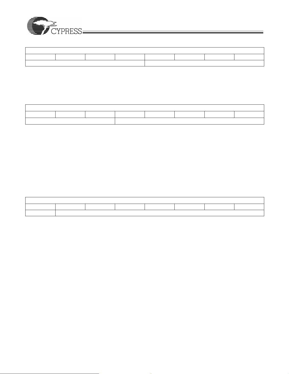
11. 0 DC Characteristics (over the operat ing range)
Table 11-1. DC Parameters
Parameter Description Conditions Min. Typ.
V
CC
V
OH1
V
OH2
V
OL
V
IH
V
IL
I
IL
C
IN
I
Sleep
IDLE I
CC
STARTUP I
TX AVG I
TX AVG I
RX I
TX I
CC
CC1
CC2
CC (PEAK)
CC (PEAK)
SYNTH SETTLE
I
CC
Notes:
10. It is permissible to connect voltages above Vcc to inputs through a series resistor limiting input current to 1 mA.
11. Typ. values measured with Vcc = 3.0V @ 25°C
12. Average Icc when transmitting a 5-byte packet (3 data bytes + 2 bytes of protocol) every 10ms using the WirelessUSB LS 1-way protocol.
13. Average Icc when transmitting a 5-byte packet (3 data bytes + 2 bytes of protocol) every 10ms using the WirelessUSB LS 2-way protocol.
Supply Voltage 2.7 3.0 3.6 V
Output High Voltage condition 1 At IOH = –100.0µA VCC–0.1 V
Output High Voltage condition 2 At IOH = –2.0 mA 2.4 3.0 V
Output Low Voltage At IOL = 2.0 mA 0.0 0.4 V
Input High Voltage 2.0 V
Input Low Voltage –0.3 0.8 V
Input Leakage Current 0 < VIN < V
CC
–1 0.26 +1 µA
Pin Input Capacitance (except X13, X13IN,
RFIN)
Current consumption during power-down mode PD = LOW 0.24 10 µA
Current consumption without synthesizer PD = HIGH 3 mA
ICC from PD high to oscillator stable. 1.8 mA
Average transmitter current consumption
Average transmitter current consumption
[12]
[13]
no handshake
with handshaking
Current consumption during receive 57.7 mA
Current consumption during transmit 69.1 mA
Current consumption with Synthesizer on, No
Transmit or Receive
[11]
CC
3.5 10 pF
5.9 mA
8.1 mA
28.7 mA
Max. Unit
V
[10
CC
V
]
Document 38-16007 Rev. *F Page 25 of 33

CYWUSB6932
CYWUSB6934
12.0 AC Characteristics
Table 12-1. SPI Interface
[16]
[14]
Parameter Description Min. Typ. Max. Unit
t
SCK_CYC
t
SCK_HI (BURST
[15]
READ)
t
SCK_HI
t
SCK_LO
t
DAT_SU
t
DAT_HLD
t
DAT_VAL
t
SS_SU
t
SS_HLD
SPI Clock Period 476 ns
SPI Clock High Time 238 ns
SPI Clock High Time 158 ns
SPI Clock Low Time 158 ns
SPI Input Data Set-up Time 10 ns
SPI Input Data Hold Time 97
SPI Output Data Valid Time 77
SPI Slave Select Set-up T ime befo re first positiv e edge of SCK
[17]
[16]
[16]
250 ns
SPI Slave Select Hold Time after last negative edge of SCK 80 ns
t
SCK_CYC
t
SCK_HI
t
SCK_LO
SCK
S
A
SS
MOSI
MISO
t
DAT_SU
t
SS_SU
M
P
L
E
t
data fro m m cu data fro m m c u
DAT_HLD
D
R
I
V
E
da ta fr o m m c u
t
DAT_VAL
data to m cu d a ta to m cu
t
SS_HLD
174
[16]
data
data
ns
ns
Figure 12-1. SPI Timing Diagram
t
SCK_CYC
SCK
SS
MISO
t
SCK_HI
every 8th SCK_HI every 9th SCK_HI every 10th SCK_HI
data to m c u data to m cu
D
R
I
V
E
t
DAT_VAL
t
SCK_LO
t
SCK_HI (BURST READ)
Figure 12-2. SPI Burst Read Every 9th SCK HI Stretch Timing Diagram
Notes:
14. AC values are not guaranteed if voltages on any pin exceed Vcc.
15. This stretch only applies to every 9th SCK HI pulse for SPI Burst Reads only.
16. For F
17. SCK must start low, otherwise the success of SPI transactions are not guaranteed.
= 13 MHz ±50ppm, 3.3v @ 25°C.
OSC
D
R
I
V
E
data to mcu
D
R
I
V
E
data
Document 38-16007 Rev. *F Page 26 of 33

CYWUSB6932
CYWUSB6934
Table 12-2. DIO Interface
Parameter Description
Transmit Min. Typ. Max. Unit
t
TX_DIOVAL_SU
t
TX_DIO_SU
t
TX_DIOVAL_HLD
t
TX_DIO_HLD
t
TX_IRQ_HI
t
TX_IRQ_LO
Receive Min. Typ. Max. Unit
t
RX_DIOVAL_VLD
t
RX_DIO_VLD
t
RX_IRQ_HI
t
RX_IRQ_LO
DIOV AL Set-u p Time 2.1 µs
DIO Set-up Time 2.1 µs
DIOVAL Hold T ime 0 µs
DIO Hold Time 0 µs
Minimum IRQ High Time - 32 chips/bit DDR 8 µs
Minimum IRQ High Time - 32 chips/bit 16 µs
Minimum IRQ High Time - 64 chips/bit 32 µs
Minimum IRQ Low Time - 32 chips/bit DDR 8 µs
Minimum IRQ Low Time - 32 chips/bit 16 µs
Minimum IRQ Low Time - 64 chips/bit 32 µs
DIOV AL Valid Time - 32 chips/bit DDR -0.01 6.1 µs
DIOVAL V a lid Time - 32 chips/bit -0.01 8.2 µs
DIOVAL V a lid Time - 64 chips/bi t -0.01 16.1 µs
DIO Va lid Time - 32 chips/bit DDR -0.01 6.1 µs
DIO V a lid Time - 32 chips/bit -0.01 8.2 µs
DIO V a lid Time - 64 chips/bit -0.01 16.1 µs
Minimum IRQ High Time - 32 chips/bit DDR 1 µs
Minimum IRQ High Time - 32 chips/bit 1 µs
Minimum IRQ High Time - 64 chips/bit 1 µs
Minimum IRQ Low Time - 32 chips/bit DDR 8 µs
Minimum IRQ Low Time - 32 chips/bit 16 µs
Minimum IRQ Low Time - 64 chips/bit 32 µs
IR Q
DIO/
DIOVAL
t
S
A
RX_IRQ_HI
M
P
L
E
data
t
RX_IRQ_LO
t
RX_DIO_VLD
t
RX_DIOVAL_VLD
S
A
M
P
L
E
data
data
Figure 12-3. DIO Receive Timing Diagram
IR Q
DIO/
DIOVAL
t
t
TX_DIO_SU
t
TX_DIOVAL_SU
TX_IRQ_HI
t
TX_IRQ_LO
S
A
M
P
L
E
data data
t
TX_DIO_HLD
t
TX_DIOVAL_HLD
S
A
M
P
L
E
Figure 12-4. DIO Transmit Timing Diagram
Document 38-16007 Rev. *F Page 27 of 33

CYWUSB6932
CYWUSB6934
12.1 Radio Parameters
Table 12-3. Radio Parameters
Parameter Description Conditions Min. Typ. Max. Unit
RF Frequency Range
Radio Receiver (T = 25°C, V
= 3.3V, fosc = 13.000 MHz, X13OUT off, 64 chips/bit, Threshold Low = 8, Threshold High = 56, BER < 10–3)
CC
Sensitivity –90 dBm
Maximum Received Sign al –20 –10 dBm
RSSI value for PWR
RSSI value for PWR
> -40 dBm 28 - 31
in
< -95 dBm 0 -10
in
Interference Performance
Co-channel Interference rejection
Carrier-to-Interference (C/I)
Adjacent (1 MHz) channel selectivity C/I 1 MHz C = –60 dBm 3 dB
Adjacent (2 MHz) channel selectivity C/I 2 MHz C = –60 dBm –30 dB
Adjacent (>
Image
3 MHz) channel selectivity C/I > 3 MHz C = –67 dBm –40 dB
[21]
Frequency Interference, C/I Image C = –67 dBm –20 dB
Adjacent (1 MHz) interference to in-band image
frequency, C/I image
±1 MHz
Out-of-Band Blocking Interference Signal Frequency
30 MHz – 2399 MHz, e xcept (FO/N & FO/N± 1 MHz)
2498 MHz – 12.75 GHz,
except (FO*N & FO*N±1 MHz)
Intermodulation C = –64 dBm,
Spurious Emission
30 MHz – 1 GHz –57 dBm
1 GHz – 12.75 GHz
except (4.8 GHz - 5.0 GHz) –47 dBm
4.8 GHz – 5.0 GHz –37
Radio Transmitter (T = 25°C, V
= 3.3V, fosc = 13.000 MHz)
CC
Maximum RF Transmit Power PA = 7 0 dBm
RF Power Control Range 30 dB
RF Power Ra nge Control Step Size seven steps, monotonic 4.3 dB
Frequency Deviation PN Code Pattern 10101010 270 kHz
Frequency Deviation P N Code Pattern 11110000 320 kHz
Zero Crossing Error
Occupied Bandwidth 100-kHz resolution bandwidth, –6 dBc 500 kHz
Initial Frequency Offset ±75 kHz
In-band Spurious
Second Channel Power (±2 MHz) –30 dBm
>
Third Channel Power (>3 MHz) –40 dBm
Non-Harmonically Related Spurs
30 MHz – 12.75 GHz –57 dBm
Harmonic Spurs
Second Harmonic –20 dBm
Third Harmonic –30 dBm
Fourth and Greater Harmonics –47 dBm
Notes:
18. FO = Tuned Frequency, N = Integer.
19. Subject to regulation.
20. Antenna matching network and antenna will attenuate the output signal at these frequencies to meet regulatory requirements.
21. Image frequency is +4 MHz from desired channel (2 MHz low IF, high side injection).
[19]
2.400 2.483 GHz
C = –60 dBm 11 dB
C = –67 dBm –25 dB
[18]
C = –67 dBm –30 dBm
[18]
C = –67 dBm –20 dBm
∆f = 5,10 MHz –39 dBm
±125 ns
[20]
dBm
Document 38-16007 Rev. *F Page 28 of 33

CYWUSB6932
CYWUSB6934
12.2 Power Management Timing
Table 12-4. Power Management Timing (The values below are dependent upon oscillator network component selection)
Parameter Description Conditions Min. Typ Max. Unit
t
PDN_X13
t
SPI_RDY
t
PWR_RST
t
RST
t
PWR_PD
t
WAKE
t
PD
t
SLEEP
t
WAKE_INT
t
STABLE
X13OUT
RESET
VCC
Time from PD deass ert to X13O UT 2000 µs
Time from oscillator stable to start of SPI transactions 1 µs
Power On to RESET deasserted Vcc @ 2.7V 1300 µs
Minimum RESET asserted pulse width 1 µs
Power On to PD deasserted
PD deassert to clocks running
[22]
[23]
1300 µs
2000 µs
Minimum PD asserted pulse width 10 µs
PD assert to low power mode 50 ns
PD deassert to IRQ
[24]
assert (wake interrupt)
[25]
2000 µs
PD deassert to clock stable to within ±10 ppm 2100 µs
t
SPI_RDY
t
RST
t
PWR_R ST
t
PDN_X13
S
T
A
R
T
U
P
PD
t
PWR_PD
Figure 12-5. Power On Reset/Reset Timing
t
X13OU T
PD
IRQ
S
L
E
t
SLEEP
E
P
t
PD
WAKE
W
A
K
E
I
R
Q
t
WAKE_INT
t
STABLE
Figure 12-6. Sleep / Wake Timing
Notes:
22. The PD
23. When X13OUT is enabled.
24. Both the polarity and the drive method of the IRQ pin are programmable. See page 10 for more details. Figure12-6 illustrates default values for the Configuration
25. A wakeup event is triggered when the PD
pin must be asserted at power up to ensure proper crystal startup.
register (Reg 0x05, bits 1:0).
register (Reg 0x1C, bit 0=1).
pin is deasserted. Figure 12-6 illustrates a wakeup event configured to trigger an IRQ pin event via the Wake Enable
Document 38-16007 Rev. *F Page 29 of 33

12.3 AC Test Loads and Waveforms for Digital Pins
CYWUSB6932
CYWUSB6934
AC Test Loads
OUTPUT
30 pF
INCLUDING
JIG AND
SCOPE
Max
Parameter Unit
R1 1071 Ω
R2 937 Ω
R
TH
V
TH
V
CC
500 Ω
1.4 V
3.00 V
OUTPUT
5 pF
INCLUDING
JIG AND
SCOPE
Typical
V
CC
GND
Rise time: 1 V/ns
Equivalent to: VENIN EQUIVALENT
OUTPUT
DC Test Load
V
CC
OUTPUT
ALL INPUT PULSES
90%
10%
THÉ
R
TH
R1
R2
90%
10%
Fall time: 1 V/ns
V
TH
Figure 12-7. AC Test Loads and Waveforms for Digital Pins
13.0 Ordering Information
Table 13-1. Ordering Information
Part Number Radio Package Name Package Type Operating Range
CYWUSB6932-28SEC Transmitter 28 SOIC 28-Lead Molded SOIC Exposed Paddle Commercial
CYWUSB6934-28SEC Transceiver 2 8 SOIC 28-Lead Molded SOIC Exposed Paddle Commercial
CYWUSB6934-48LFC Transceiver 48 QFN 48 Quad Flat Package No Leads Commercial
Document 38-16007 Rev. *F Page 30 of 33

14.0 Package Description
The CYWUSB6932/CYWUSB6934 ICs come in a 28-pin
exposed paddle SOIC package.
PIN 1 ID
114
0.394[10.01]
0.419[10.64]
0.291[7.39]
0.300[7.62]
DIMENSIONS IN INCHES[MM]
REFERENCE JEDEC MS-013
PACKAGE WEIGHT 0.8gms
PART #
SE28.3 STANDARD PKG.
SA28.3 LEAD FREE PKG.
1
E-PAD
MIN.
MAX.
CYWUSB6932
CYWUSB6934
14
15 28
TOP VIEW BOTTOM VIEW
0.050[1.27]
TYP.
0.697[17.70]
0.713[18.11]
0.013[0.33]
0.019[0.48]
0.026[0.66]
0.032[0.81]
0.092[2.33]
0.105[2.67]
0.004[0.10]
0.0118[0.30]
SEATING PLANE
0.004[0.10]
28
0.015[0.38]
0.050[1.27]
15
0.0091[0.23]
0.0125[3.17]
51-85184-*A
Figure 14-1. 28-pin (300-Mil) SOIC EPAD SE28.3 SOIC
The recommend dimension of the PCB pad size for the E-PAD underneath the SOIC is 190 mils × 225 mils (width × length).
0.08
0.05 MAX.
0.20 REF.
C
X
0.23±0.05
E-PAD
Y
PIN1 ID
0.20 R.
N
1
2
0.45
5.45
5.55
0.80 DIA.
6.90
7.10
6.70
N
1
2
6.80
6.70
6.80
6.90
7.10
1.00 MAX.
0.80 MAX.
0.30-0.45
0.42±0.18
(4X)
51-85152-*B
TOP VIEW
DIMENSIONS IN mm MIN.
MAX.
REFERENCE JEDEC MO-220
PKG. WEIGHT 0.13 gms
0°-12°
SIDE VIEW
0.50
C
SEATING
PLANE
5.45
5.55
BOTTOM VIEW
E-PAD SIZE PADDLE SIZE
(X, Y MAX.)
5.1 X 5.1
5.3 X 5.3
3.8 X 3.8 4.0 X 4.0
Figure 14-2. 48-pin QFN 7 x 7 mm LF48
Document 38-16007 Rev. *F Page 31 of 33

The recommended dimension of the PCB pad size for the
E-PAD underneath the QFN is 209 mils × 209 mils (width x
length).
CYWUSB6932
CYWUSB6934
This document is subje ct to cha nge , and may be fo und to contain errors of omis s ion or cha nge s in p ara me ters . For fee db ack or
technical support regarding Cypress WirelessUSB products please contact Cypress at www.cypress.com. WirelessUSB and
enCoRe are trademark s o f Cypr ess Sem ic on duc tor. All product and company names m en t io ned in th is d oc um ent a re the trad emarks of their respective holders.
Document 38-16007 Rev. *F Page 32 of 33
© Cypress Semiconductor Corporation, 2004. The informat i on cont ained her ein i s subject to change with out notice. Cy pr ess Semiconducto r Corporation assu mes no respo nsibility for the use
of any circuitry other than circuitry embodied in a Cypress product. Nor does it convey or imply any license under patent or other rights. Cypress products are not warranted nor intended to be
used for medical, life support, life saving, critical control or safety applications, unless pursuant to an express written agreement with Cypress. Furthermore, Cypress does not authorize its
products for use as critical components in life-support systems where a malfunction or failure may reasonably be expected to result in significant injury to the user. The inclusion of Cypress

CYWUSB6932
CYWUSB6934
Document History Page
Document Title: CYWUSB6932/CYWUSB6934 WirelessUSB™ LS 2.4 GHz DSSS Radio SoC
Document Number: 38-16007
REV. ECN NO. Issue Date
** 123907 01/20/03 LXA New Data Sheet
*A 125470 04/28/03 XGR Preliminary Release
*B 127076 07/30/03 KKU Updated pins outs, timing diag rams, AC T es t loads, DC Characteri stics, Radio
*C 128886 08/04/03 KKV Minor change: removed table of contents and fixed layout of section 10.
*D 129180 12/04/03 TGE Updated AC and DC characteristics from char. results
*E 131851 12/15/03 TGE Changed Static Discharge Voltage (Digital) Specification of Section 9.0
*F 241471 See ECN ZTK Removed Static Discharge Voltage (Digital) Specification of Section 9.0
Orig. of
Change Description of Change
Characteristics
Removed die
Updated register entries
Changed package type from 56-pin QFN to 48-pin QFN
Updated all pinouts and timing diagrams
Updated block diagram and functional description
Updated application interfa ces
Added Interrupt descriptions
Footnote
Updated REG_DATA_RATE (0x04), 111 - Not Valid
Swapped bit field descriptions of REG_CONFIG
Corrected Figures 3-1 and 6-2. Minor edit s thro ugh out
Document 38-16007 Rev. *F Page 33 of 33
 Loading...