

Page 1

r
CYV15G0404RB
Independent Clock Quad HOTLink II™
Deserializing Reclocke
Features
• Second-generation HOTLink® technology
• Compliant to SMPTE 292M and SMPTE 259M video
standards
• Quad channel video reclocking deserializer
— 195 to 1500 Mbps serial data signaling rate
— Simultaneous operation at different signaling rates
• Supports reception of either 1.485 or 1.485/1.001 Gbps data
rate with the same training clock
• Supports half-rate and full-rate clocking
• Internal phase-locked loops (PLLs) with no external PLL
components
• Selectable differential PECL-compatible serial inputs
— Internal DC restoration
• Synchronous LVTTL parallel interface
• JTAG boundary scan
• Built-In Self-Test (BIST) for at-speed link testing
• Link Quality Indicator
— Analog signal detect
— Digital signal detect
• Low-power: 3W @ 3.3V typical
• Single 3.3V supply
• Thermally enhanced BGA
• Pb-Free package option available
•0.25µ BiCMOS technology
Functional Description
The C YV15G0404RB Ind ependent Clock Quad HOT Link II™
Deserializing Reclocker is a point-to-point or point-to-multipoint communications building block enabling data transfer
over a variety of high speed se ri al li n ks i n cl ud i n g SMPTE 292
and SMPTE 259 video applications. It supports signaling rates
in the range of 195 to 1500 Mbps for each serial link. The four
channels are independent and can simultaneously operate at
different rates. Each receive channel accepts serial data and
converts it to 10-bit parallel characters and presents these
characters to an Output Register. The received serial data can
also be reclocked and retransmitted through the reclocker
serial outputs. Figure 1, "HOTLink II™ System Connections,"
on page 2 illustrates typical connections between independent
video coprocessors and corresponding CYV15G0404RB
Reclocking Deserializer and CYV15G0403TB Serializer chips.
The CYV15G0404RB is SMPTE-259M and SMPTE-292M
compliant according to SMPTE EG34-1999 Pathological Test
Requirements.
As a second generation HOTLink device, the
CYV15G0404RB extends the HOTLink family with enhanced
levels of integration and faster data rates, while maintaining
serial-link compatibility (data and BIST) with other HOTLink
devices.
Each channel of the CYV15G0404RB Quad HOTLink II device
accepts a serial bit-stream from one of two selectable
PECL-compatible differential line receivers, and using a
completely integrated Clock and Data Recovery PLL, recovers
the timing information necessary for data reconstruction. The
device reclocks and retransmits recovered bit-stream through
the reclocker serial outputs. It also deserializes the recovered
serial data and presents it to the destination host system.
Each channel contains an independent BIST pattern checker.
This BIST hardware enables at speed testing of the
high-speed serial data paths in each receive section of this
device, each transmit section of a connected HOTLink II
device, and across the interconnecting links.
The CYV15G0404RB is ideal for SMPTE applications where
different data rates and serial interface standards are
necessary for each channel. Some applications include
multi-format routers, switchers, format converters, SDI
monitors, and camera control units.
Cypress Semiconductor Corporation • 198 Champion Court • San Jose, CA 95134-1709 • 408-943-2600
Document #: 38-02102 Rev. *C Revised February 16, 2007
[+] Feedback
Page 2
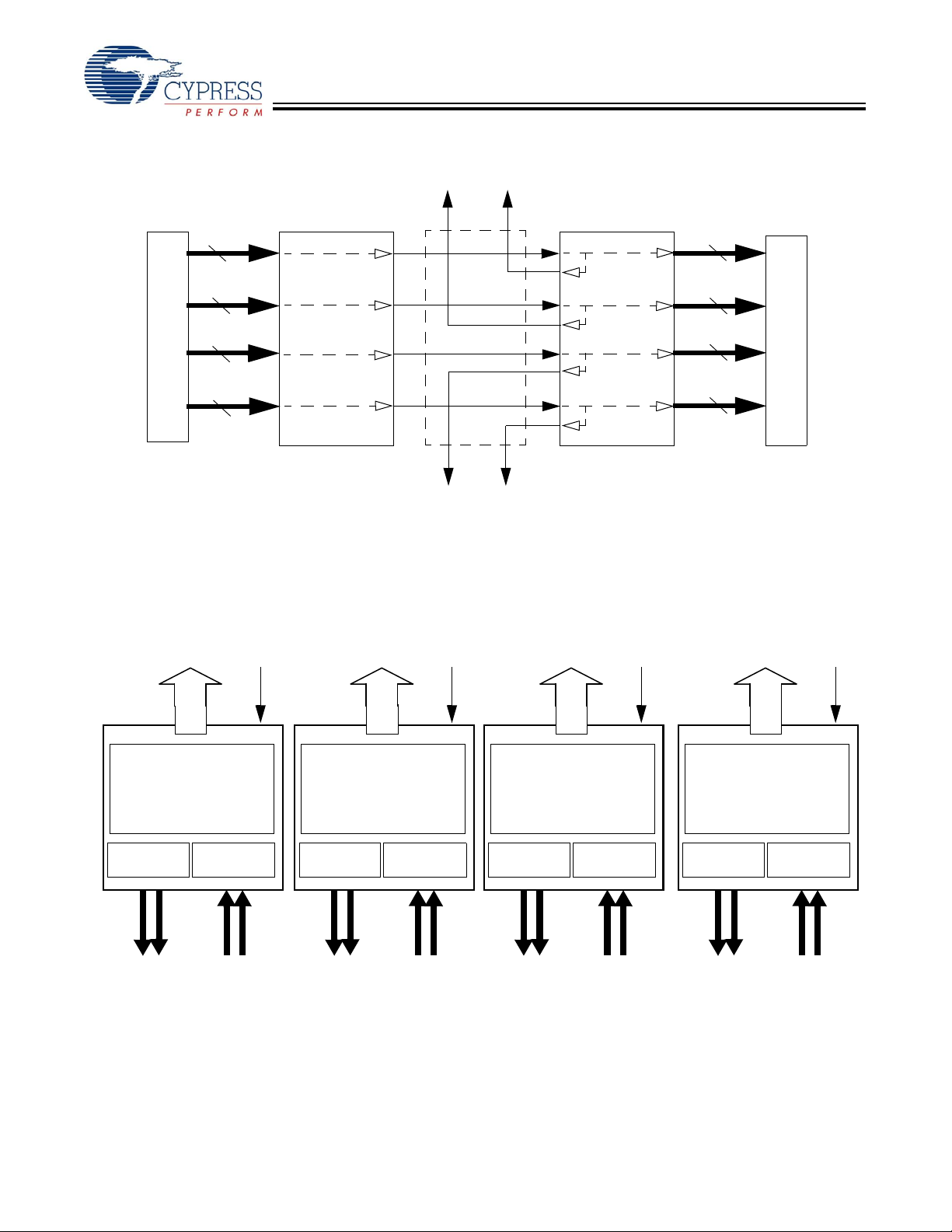
Figure 1. HOTLink II™ System Connections
Reclocked
Outputs
CYV15G0404RB
10
Video Coprocesso r
10
Independent
Channel
10
10
CYV15G0403TB
Serializer
Serial Links
Reclocked
Outputs
Reclocking Deserializer
CYV15G0404RB Deserializing Reclocker Logic Block Diagram
RXDA[9:0]
TRGCLKA±
RXDB[9:0]
TRGCLKB±
RXDC[9:0]
Independent
Channel
CYV15G0404RB
TRGCLKC±
10
10
10
Video Coprocessor
10
RXDD[9:0]
TRGCLKD±
Deserializer
Reclocker
ROUTA1±
ROUTA2±
x10
RX
INA1±
x10
Deserializer
Reclocker
INA2±
ROUTB1±
ROUTB2±
RX
INB1±
Reclocker
INB2±
x10
Deserializer
±
±
ROUTC1
ROUTC2
RX
±
INC1
x10
Deserializer
Reclocker
±
±
INC2
±
ROUTD1
ROUTD2
RX
±
IND1
±
IND2
Document #: 38-02102 Rev. *C Page 2 of 27
[+] Feedback
Page 3
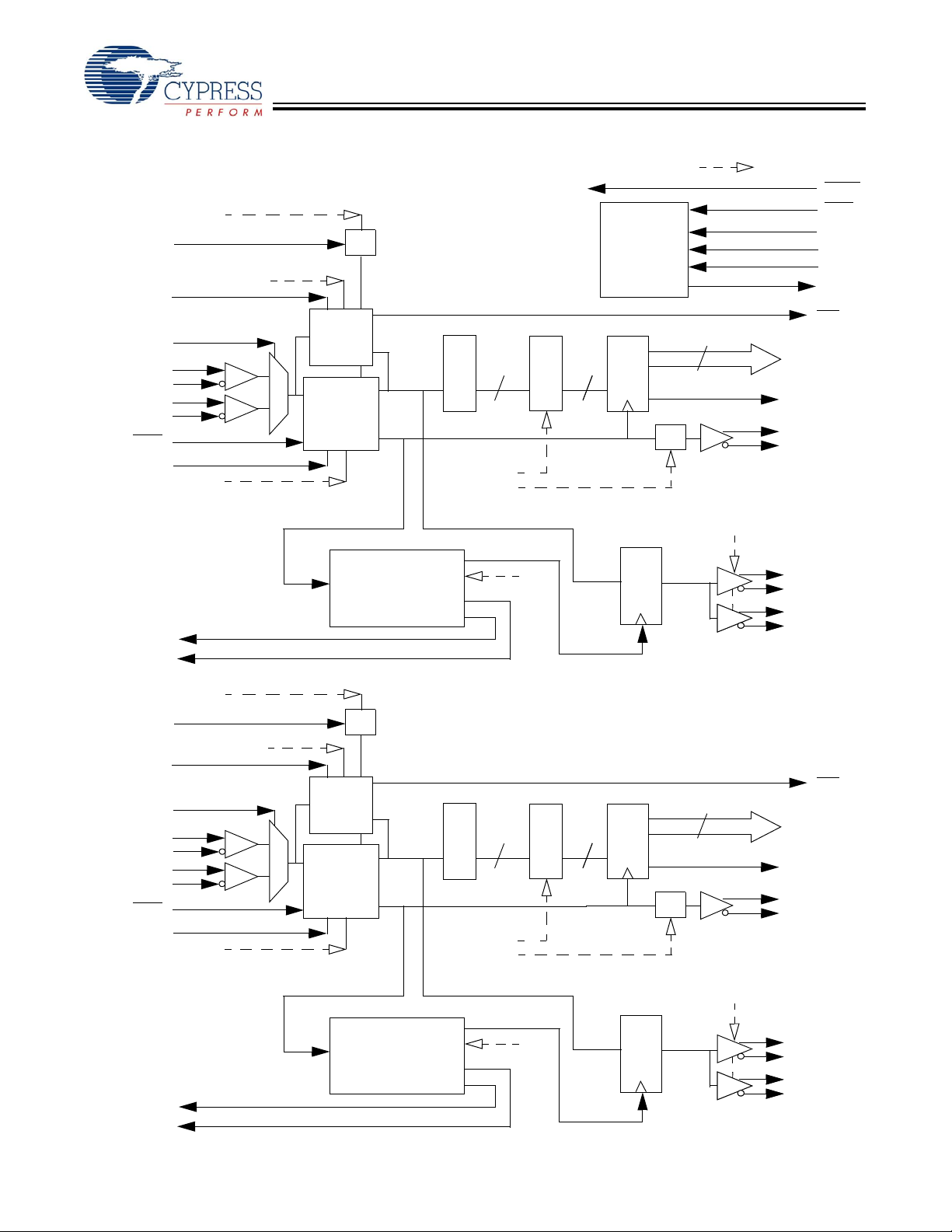
CYV15G0404RB
Reclocking Deserializer Path Block Diagram
TRGRATEA
TRGCLKA
SDASEL[2..1]A[1:0]
LDTDEN
INSELA
INA1+
INA1–
INA2+
INA2–
ULCA
SPDSELA
RXPLLPDA
Recovered Character Clock
RECLKOA
REPDOA
x2
Receive
Signal
Monitor
Clock &
Data
Recovery
PLL
Recovered Serial Data
Reclocker
Output PLL
Clock Multiplier A
Character-Rate Clock A
10
Shifter
RXBISTA[1:0]
RXRATEA
ROE[2..1]A
10
BIST LFSR
JTAG
Boundary
Scan
Controller
Output
Register
÷2
Register
10
ROE[2..1]A
= Internal Signal
RESET
TRST
TMS
TCLK
TDI
TDO
LFIA
RXDA[9:0]
BISTSTA
RXCLKA+
RXCLKA–
ROUTA1+
ROUTA1–
ROUTA2+
ROUTA2–
TRGCLKB
LDTDEN
INSELB
INB1+
INB1–
INB2+
INB2–
ULCB
SPDSELB
RECLKOB
REPDOB
TRGRATEB
SDASEL[2..1]B[1:0]
RXPLLPDB
x2
Receive
Signal
Monitor
Clock &
Data
Recovery
PLL
Recovered Character Clock
Reclocker
Output PLL
Clock Multiplier B
Character-Rate Clock B
10
Shifter
RXBISTB[1:0]
RXRATEB
Recovered Serial Data
ROE[2..1]B
10
BIST LFSR
Output
Register
Register
÷2
10
ROE[2..1]B
LFIB
RXDB[9:0]
BISTSTB
RXCLKB+
RXCLKB–
ROUTB1+
ROUTB1–
ROUTB2+
ROUTB2–
Document #: 38-02102 Rev. *C Page 3 of 27
[+] Feedback
Page 4
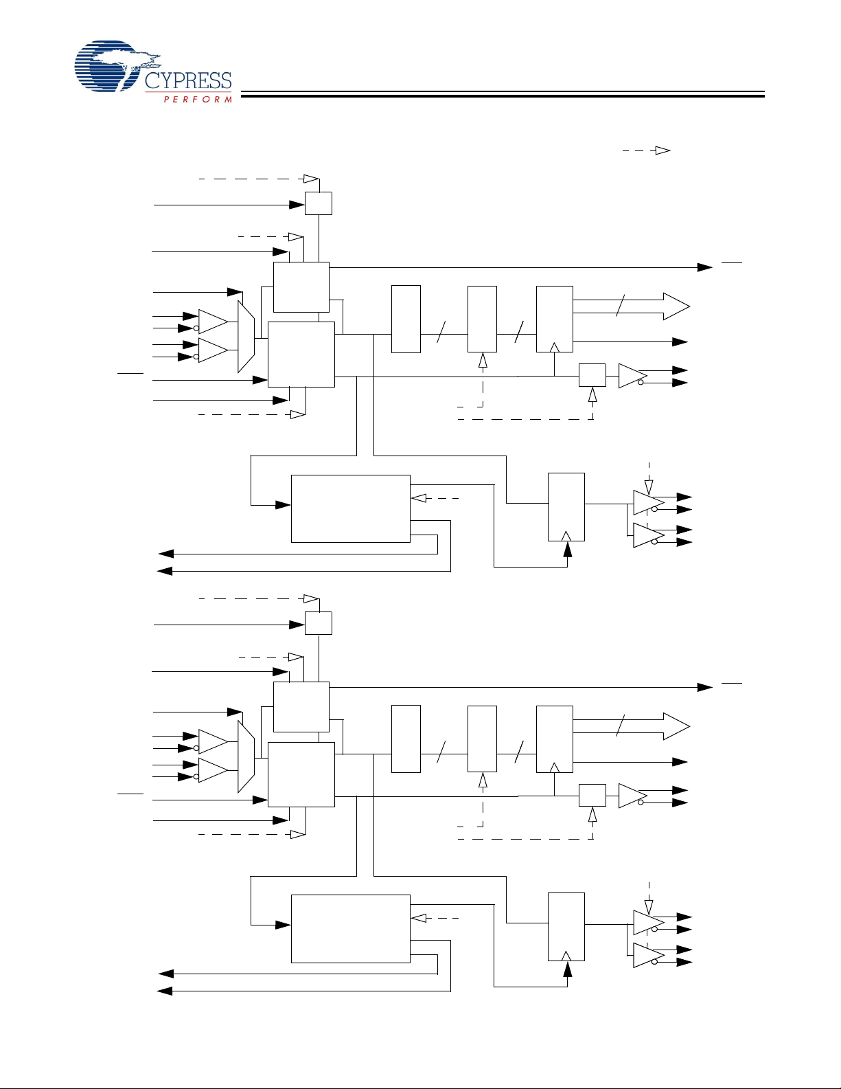
CYV15G0404RB
Reclocking Deserializer Path Block Diagram (continued)
TRGRATEC
TRGCLKC
SDASEL[2..1]C[1:0]
LDTDEN
INSELC
INC1+
INC1–
INC2+
INC2–
ULCC
SPDSELC
RXPLLPDC
Recovered Character Clock
RECLKOC
REPDOC
x2
Receive
Signal
Monitor
Clock &
Data
Recovery
PLL
Reclocker
Output PLL
Clock Multiplier C
Character-Rate Clock C
10
Shifter
RXBISTC[1:0]
RXRATEC
Recovered Serial Data
ROE[2..1]C
10
BIST LFSR
Output
Register
Register
÷2
10
ROE[2..1]C
= Internal Signal
LFIC
RXDC[9:0]
BISTSTC
RXCLKC+
RXCLKC–
ROUTC1+
ROUTC1–
ROUTC2+
ROUTC2–
TRGCLKD
LDTDEN
INSELD
IND1+
IND1–
IND2+
IND2–
ULCD
SPDSELD
RECLKOD
REPDOD
TRGRATED
SDASEL[2..1]D[1:0]
RXPLLPDD
x2
Receive
Signal
Monitor
Clock &
Data
Recovery
PLL
Recovered Character Clock
Reclocker
Output PLL
Clock Multiplier D
Character-Rate Clock D
10
Shifter
RXBISTD[1:0]
RXRATED
Recovered Serial Data
ROE[2..1]D
10
BIST LFSR
Output
Register
Register
÷2
10
ROE[2..1]D
LFID
RXDD[9:0]
BISTSTD
RXCLKD+
RXCLKD–
ROUTD1+
ROUTD1–
ROUTD2+
ROUTD2–
Document #: 38-02102 Rev. *C Page 4 of 27
[+] Feedback
Page 5
CYV15G0404RB
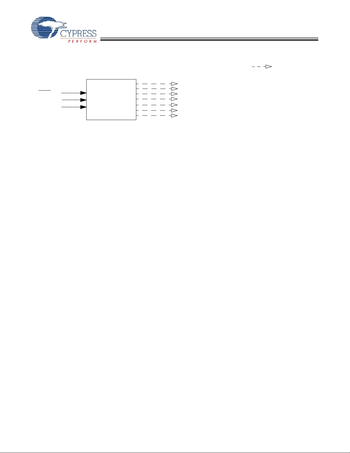
Device Configuration and Control Block Diagram
WREN
ADDR[3:0]
DATA[7:0]
Device Configuration
and Control Interface
= Internal Signal
RXBIST[A..D]
RXRATE[A..D]
SDASEL[A..D][1:0]
RXPLLPD[A..D]
ROE[2..1][A..D]
GLEN[11..0]
FGLEN[2..0]
Document #: 38-02102 Rev. *C Page 5 of 27
[+] Feedback
Page 6

CYV15G0404RB
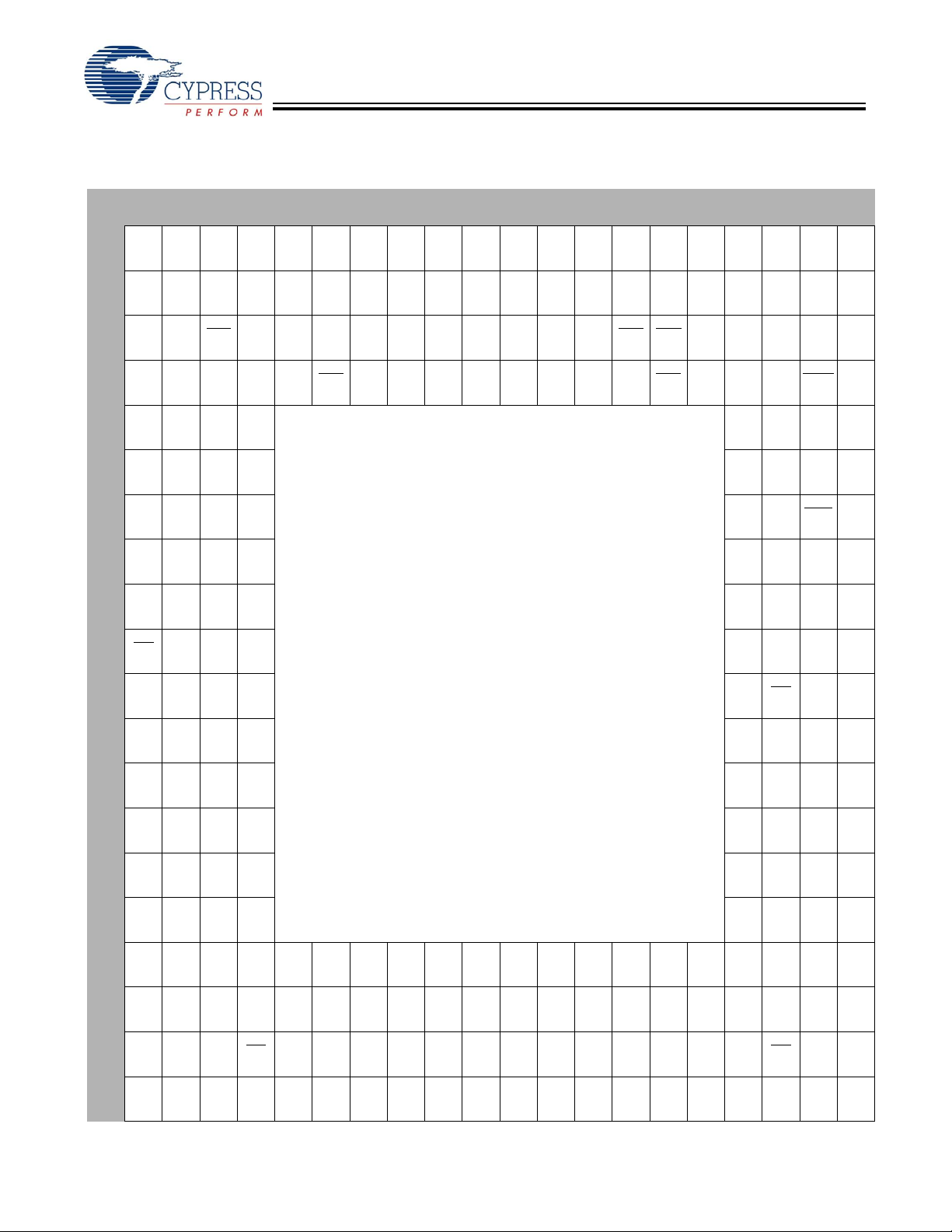
Pin Configuration (Top View)
[1]
1 2 3 4 5 6 7 8 9 10 11 12 13 14 15 16 17 18 19 20
A
IN
ROUT
C1–
C1–INC2–
B
IN
ROUT
C1+
C1+INC2+
C
TDI TMS INSELC INSELB
D
TCLK RESET INSELD INSELA
E
VCCVCCVCCV
F
RX
DC[8]RXDC[9]
G
H
J
K
L
M
N
WREN
GND
GND GND GND GND GND GND GND GND
GND GND GND GND
RX
TRG
DC[4]
CLKC–
RX
TRG
DC[5]
CLKC+
RX
DC[6]RXDC[7]
GND GND GND GND GND GND GND GND
ROUT
C2–
ROUT
C2+
CC
VCCV
CC
GND GND
GND GND
LFIC
GND
RE
V
CC
PDOC
V
CC
V
CC
V
CC
V
CC
IN
ROUT
D1–
D1–
IN
ROUT
D1+
D1+
ULCD ULCC
ULCA SPD
SELC
GND
GND
GND
GND
IN
D2–
IN
D2+
DATA
[7]
DATA
[6]
ROUT
D2–INA1–
ROUT
D2+INA1+
DATA
[5]
DATA
[4]
DATA
[3]
DATA
[2]
ROUT
A1–
ROUT
A1+
DATA
[1]
DATA
[0]
IN
GND
A2–
IN
GND
A2+
GND V
CC
GND GND
ROUT
A2–
ROUT
A2+
SPD
SELD
ULCB
IN
V
CC
B1–
IN
V
CC
B1+
LDTD ENTRST
V
CC
V
NC V
CC
VCCVCCVCCV
V
CC
SPD
SELB
BIST
STBRXDB[2]RXDB[7]RXDB[4]
RX
DB[5]RXDB[6]RXDB[9]
RX
DB[8]RXCLKB+RXCLKB–
TRG
CLKB+
CLKB–REPDOB
ROUT
B1–INB2–
ROUT
B1+INB2+
CC
RX
DB[0]RECLKOBRXDB[1]
NC
ROUT
B2–
ROUT
B2+
TDO
GND
SCAN
TMEN3
EN2
SPD
SELARXDB[3]
LFIB
GND
TRG
GND
CC
P
RX
DC[3]RXDC[2]RXDC[1]RXDC[0]
R
BIST
STCRECLKOCRXCLKC+RXCLKC–
T
VCCVCCVCCV
U
VCCVCCVCCVCCV
V
VCCVCCV
W
VCCV
CC
Y
VCCV
CC
Note
1. NC = Do not connect.
CC
DD[8]
LFID RX
CLKD–
RX
DD[9]
CLKD+
RX
RX
CC
CC
V
CC
V
CC
V
CC
RX
DD[4]RXDD[3]
RX
DD[5]RXDD[1]
RX
DD[6]RXDD[0]
RX
DD[7]RXDD[2]
GND GND
BIST
GND
STD
ADDR
GND
[3]
RE
GND
CLKOD
ADDR
TRG
[0]
CLKD–
ADDR
TRG
[2]
CLKD+RECLKOA
ADDR
[1]RXCLKA+REPDOA
NC
GND
CLKA–
GND GND GND VCCV
GND GND VCCV
GND GND VCCV
RX
GND GND VCCV
GND GND GND GND
VCCVCCVCCV
VCCVCCVCCV
RX
CC
CC
CC
CC
V
DA[4]
DA[9]RXDA[5]RXDA[2]RXDA[1]
PDOD
CC
RX
LFIA TRG
CLKA+RXDA[6]RXDA[3]
RE
TRG
CLKA–RXDA[8]RXDA[7]
BIST
STARXDA[0]
CC
CC
Document #: 38-02102 Rev. *C Page 6 of 27
[+] Feedback
Page 7
CYV15G0404RB
Pin Configuration (Bottom View)
[1]
20 19 18 17 16 15 14 13 12 11 10 9 8 7 6 5 4 3 2 1
ROUT
A
B2–INB2–
ROUT
B
B2+INB2+
TDO
C
TMEN3 SCAN
D
VCCVCCVCCV
E
RX
F
DB[1]RECLKOBRXDB[0]
RX
G
DB[3]
GND GND GND GND GND GND GND GND
H
RX
J
DB[4]RXDB[7]RXDB[2]
GND
EN2
SPD
SELA
ROUT
B1–INB1–
ROUT
B1+INB1+
TRST LDTD
EN
V
NC V
CC
CC
V
CC
SPD
NC
SELB
BIST
STB
V
V
V
CC
CC
CC
CC
ROUT
A2–INA2–
ROUT
A2+INA2+
SPD
SELD
ULCB
GND
GND
VCCGND
GND GND
ROUT
A1–INA1–
ROUT
A1+INA1+
DATA
[1]
DATA
[0]
DATA
[3]
DATA
[2]
ROUT
D2–IND2–
ROUT
D2+IND2+
DATA
[5]
DATA
[4]
DATA
[7]
DATA
[6]
GND
GND
GND
GND
ROUT
D1–IND1–
ROUT
D1+IND1+
ULCC ULCD
SPD
ULCA
SELC
ROUT
V
CC
C2–INC2–
ROUT
V
CC
C2+INC2+
INSELB INSELC TMS TDI
V
CC
INSELA INSELD RESET TCLK
V
CC
VCCVCCVCCV
VCCV
GND GND
GND GND GND GND
CC
ROUT
C1–INC1–
ROUT
C1+INC1+
RX
DC[9]RXDC[8]
WREN
GND
CC
LFIB RX
K
L
M
N
P
R
T
U
V
W
Y
DB[9]RXDB[6]RXDB[5]
RX
GND
CLKB–RXCLKB+RXDB[8]
RE
TRG
GND
PDOB
CLKB–
TRG
CLKB+
GND GND GND GND GND GND GND GND
GND GND GND GND
VCCVCCVCCV
VCCVCCVCCV
RX
BIST
DA[0]
STA
RX
DA[1]RXDA[2]RXDA[5]RXDA[9]
RX
DA[3]RXDA[6]
RX
DA[7]RXDA[8]
CLKA+
CLKA–REPDOD
V
CC
TRG
TRG
CC
CC
RX
VCCVCCGND GND GND
DA[4]
VCCVCCGND GND
LFIA
VCCVCCGND GND
VCCVCCGND GND
TRG
CLKD–
RE
TRG
CLKOA
CLKD+
RE
PDOARXCLKA+
RX
GND
CLKA–
ADDR
[0]
ADDR
[2]
ADDR
[1]
NC RE
GND GND
BIST
GND
STD
ADDR
GND
[3]
GND
CLKOD
RX
DD[3]RXDD[4]
RX
DD[1]RXDD[5]
RX
DD[0]RXDD[6]
RX
DD[2]RXDD[7]
GND GND
LFIC TRG
GND
RE
V
PDOC
DC[0]RXDC[1]RXDC[2]RXDC[3]
CLKC–RXCLKC+RECLKOC
CC
RX
RX
VCCVCCVCCV
VCCVCCVCCVCCV
RX
V
CC
V
CC
V
CC
VCCVCCV
DD[8]
RX
LFID
CLKD–
RX
CLKD+RXDD[9]
TRG
CLKC–RXDC[4]
CLKC+RXDC[5]
RX
DC[7]RXDC[6]
BIST
STC
CC
CC
CC
VCCV
CC
VCCV
CC
Document #: 38-02102 Rev. *C Page 7 of 27
[+] Feedback
Page 8

Pin Definitions
CYV15G0404RB Quad HOTLink II Deserializing Reclocker
Name IO Characteristics Signal Description
Receive Path Data and Status Signals
RXDA[9:0]
RXDB[9:0]
RXDC[9:0]
RXDD[9:0]
BISTSTA
BISTSTB
BISTSTC
BISTSTD
REPDOA
REPDOB
REPDOC
REPDOD
Receive Path Clock Signals
TRGCLKA±
TRGCLKB±
TRGCLKC±
TRGCLKD±
RXCLKA±
RXCLKB±
RXCLKC±
RXCLKD±
RECLKOA
RECLKOB
RECLKOC
RECLKOD
Device Control Signals
RESET
LVTTL Output,
synchronous to the
RXCLK± output
LVTTL Output,
synchronous to the
RXCLKx± output
Asynchronous to
reclocker output
channel
enable / disable
Differential LVPECL or
single-ended
LVTTL input clock
LVTTL Output Clock Receive Clock Output. RXCLKx± is the receive interface clock that controls
LVTTL Output Reclocker Clock Output
LVTTL Input,
asynchronous,
internal pull up
Parallel Data Output. RXDx[9:0] parallel data outputs change relative to the
receive interface clock. If RXCLKx± is a full-rate clock, the RXCLKx± clock outputs
are complementary clocks operating at the character rate. The RXDx[9:0] outputs
for the associated receive channels follow the rising edge of RXCLKx+ or the
falling edge of RXCLKx–. If RXCLKx± is a half-rate clock, the RXCLKx± clock
outputs are complementary clocks operating at half the character rate. The
RXDx[9:0] outputs for the associated receive channels follow both the falling and
rising edges of the associated RXCLKx± clock outputs.
When BIST is enabled on the receive channel, the RXDx[1:0] and BISTSTx
outputs present the BIST status. See Table 5, “Receive BIST Status Bits,” on
page 17 for each status that the BIST state machine reports. Also, while BIST is
enabled, ignore the RXDx[9:2] outputs.
BIST Status Outp ut. When RXBISTx[1:0] = 10, BISTSTx (along with RXDx[1:0])
displays the status of the BIST reception. See T able 5, “Receive BIST S tat us Bits,”
on page 17 for the BIST status for each combination of BISTSTx and RXDx[1:0].
When RXBISTx[1:0] ≠ 10, ignore BISTSTx.
Reclocker Powered Down Status Output. REPDOx asserts HIGH when the
associated channel’s reclocker output logic powers down. This occurs when
disabling ROE2x and ROE1x by setting ROE2x = 0 and ROE1x = 0.
CDR PLL Training Clock. The frequency detector (Range Controller) of the
associated receive PLL uses the TRGCLKx± clock inputs as the reference source
to reduce PLL acquisition time.
In the presence of valid serial data, the recovered clock output of the receive CDR
PLL (RXCLKx±) has no frequency or phase relationship with TRGCLKx±.
When a single-ended LVCMOS or LVTTL clock source drives the clock, connect
the clock source to either the true or complement TRGCLKx input, and leave the
alternate TRGCLKx input open (floating). When an LVPECL clock source drives
it, the clock must be a differential clock, using both inputs.
timing of the RXDx[9:0] parallel outputs. These true and complement clocks
control timing of data output transfers. These clocks output continuously at either
the half-character rate (1/20 the serial bit-rate) or character rate (1/1 0 the serial
bit-rate) of the data being received, as selected by RXRATEx.
. The associated reclocker output PLL synthesizes the
RECLKOx output clock, which operates synchronous to the internal recovered
character clock. RECLKOx operates at either the same frequency as RXCLKx±
(RXRATEx = 0), or at twice the frequency of RXCLKx± (RXRATEx = 1). The
reclocker clock outputs have no fixed phase relationship to RXCLKx±.
Asynchronous Device Reset. RESET initializes all state machines, counters,
and configuration latches in the device to a known state. RESET
for a minimum pulse width. When the reset is removed, all state machines,
counters and configuration latches are at an initial state. According to the JTAG
specifications, the device RESET
JTAG controller has to be reset separately. Refer to “JTAG Support” on page 17
for the methods to reset the JTAG state machine. See Table 3, “Device Configu-
ration and Control Latch Descriptions,” on page 14 for the in itialize values of the
device configuration latches.
CYV15G0404RB
must assert LOW
cannot reset the JTAG controller . Therefore, the
Document #: 38-02102 Rev. *C Page 8 of 27
[+] Feedback
Page 9
CYV15G0404RB
Pin Definitions (continued)
CYV15G0404RB Quad HOTLink II Deserializing Reclocker
Name IO Characteristics Signal Description
LDTDEN LVTTL Input,
internal pull up
ULCA
ULCB
LVTTL Input,
internal pull up
ULCC
ULCD
[2]
SPDSELA
SPDSELB
3-Level Select
static control input
SPDSELC
SPDSELD
INSELA
INSELB
LVTTL Input,
asynchronous
INSELC
INSELD
LFIA
LFIB
LVTTL Output,
asynchronous
LFIC
LFID
Device Configuration and Control Bus Signals
WREN
LV TTL input,
asynchronous,
internal pull up
ADDR[3:0] LVTTL input
asynchronous,
internal pull up
Notes
2. Use 3-Level Select inputs for static configuration. These are ternary input s th at use logic le vels of L OW, MID, and HIGH. To implement the LOW level, connect
directly to V
which allows it to self bias to the proper level.
3. See “Device Configuration and Control Interface” on page13 for detailed information about the operation of the Configuration Interface.
(ground). To implement the HIGH level, connect directly to VCC (power). To implement the MID level, do not connect the input (leave floating),
SS
Level Detect Transition Density Enable. When LDTDEN is HIGH, the Signal
Level Detector, Range Controller, and Transition Density Detector are all enabled
to determine if the RXPLL tracks TRGCLKx± or the selected input serial data
stream. If the Signal Level Detector, Range Controller, or Transition Density
Detector are out of their respective limits while LDTDEN is HIGH, the RXPLL locks
to TRGCLKx± until they become valid. The SDASEL[A..D][1:0] inputs configure
the trip level of the Signal Level Detector. The Transition Density Detector limit is
one transition in every 60 consecutive bits. When LDTDEN is LOW, only the
Range Controller determines if the RXPLL tracks TRGCLKx± or the selected input
serial data stream. Set LDTDEN = HIGH.
Use Local Clock. When ULCx is LOW, the RXPLL locks to TRGCLKx± instead
of the received serial data stream. While ULCx
is LOW, the LFIx for the associ ated
channel is LOW, indicating a link fault.
When ULCx
is HIGH, the RXPLL performs Clock and Data Recovery functions on
the input data streams. This function is used in applications that need a stable
RXCLKx±. When valid data transitions are absent for a long time, or the high-gain
differential serial inputs (INx±) are left floating, the RXCLKx± outputs may briefly
be different from TRGCLKx±.
Serial Rate Select. The SPDSELx inputs specify the operating signaling-rate
range of each channel’s receive PLL.
LOW = 195–400 MBd
MID = 400–800 MBd
HIGH = 800–1500 MBd.
Receive Input Selector. The INSELx input determines which external serial bit
stream passes to the receiver’s Clock and Data Recovery circuit. When INSELx
is HIGH, the Primary Differential Serial Data Input, INx1±, is the associated receive
channel. When INSELx is LOW, the Secondary Differential Serial Data Input,
INx2±, is the associated receive channel.
Link Fault Indication Output. LFIx is an output status indicator signal. LFIx is the
logical OR of six internal conditions. LFIx
asserts LOW when any of the following
conditions is true:
• Received serial data rate is outside expected range
• Analog amplitude is below expected levels
• Transition density is lower than expected
• Receive is channel disabled
is LOW
•ULCx
• TRGCLKx± is absent.
Control Write Enable. The WREN input writes the values of the DATA[7:0] bus
into the latch specified by the address location on the ADDR[3:0] bus.
[3]
Control Addressing Bus. The ADDR[3:0] bus is the input address bus that
configures the device. The WREN
into the latch specified by the address location on the ADDR[3:0] bus.
input writes the values of the DATA[7:0] bus
[3]
Table 3,
“Device Configuration and Control Latch Descriptions,” on page 14 lists the config-
uration latches within the device, and the initiali zation value of the latches when
RESET
is asserted. Table 4, “Device Control Latch Configuration Table,” on
page 16 shows how the latches are mapped in the device.
Document #: 38-02102 Rev. *C Page 9 of 27
[+] Feedback
Page 10

Pin Definitions (continued)
CYV15G0404RB Quad HOTLink II Deserializing Reclocker
Name IO Characteristics Signal Description
DATA[7:0] LVTTL input
asynchronous,
internal pull-up
Internal Device Configuration Latches
RXRATE[A..D] Internal Latch
SDASEL[2..1][A..D]
Internal Latch
[4]
[4]
[1:0]
RXPLLPD[A..D] Internal Latch
RXBIST[A..D][1:0] Internal Latch
ROE2[A..D] Internal Latch
ROE1[A..D] Internal Latch
GLEN[11..0] Internal Latch
FGLEN[2..0] Internal Latch
[4]
[4]
[4]
[4]
[4]
[4]
Factory Test Modes
SCANEN2 LVTTL input,
internal pull down
TMEN3 LVTTL input,
internal pull down
Analog I/O
ROUTA1±
ROUTB1±
CML Differential
Output
ROUTC1±
ROUTD1±
ROUTA2±
ROUTB2±
CML Differential
Output
ROUTC2±
ROUTD2±
INA1±
Differential Input Primary Differential Serial Data Input. The INx1± input accepts the serial data
INB1±
INC1±
IND1±
INA2±
Differential Input Secondary Differential Serial Data Input. The INx2± input accepts the serial
INB2±
INC2±
IND2±
JTAG Interface
TMS LVTTL Input,
internal pull up
TCLK LVTTL Input,
internal pull down
Note
4. See Device Configuration and Control Interface for detailed information on the internal latches.
Control Data Bus. The DATA[7:0] bus is the input data bus that configures the
device. The WREN
input writes the values of the DATA[7:0] bus into the latch
specified by address location on the ADDR[3:0] bus.
ration and Control Latch Descriptions,” on page 14 lists the configuration latches
within the device, and the initialization value of the latches when RESET is
asserted. Table 4, “Device Control Latch Configuration T able,” on page 16 shows
the way the latches are mapped in the device.
Receive Clock Rate Select.
Signal Detect Amplitude Select.
Receive Channel Power Control.
Receive BIST Disabled.
Reclocker Differential Serial Output Driver 2 Enable.
Reclocker Differential Serial Output Driver 1 Enable.
Global Latch Enable.
Force Global Latch Enable.
Factory Test 2. The SCANEN2 input is for factory testing only. Leave this input
as a NO CONNECT, or GND only.
Factory Test 3. The TMEN3 input is for factory testing only . Leave this input as a
NO CONNECT, or GND only.
Primary Differential Serial Data Output. The ROUTx1± PECL-compatible CML
outputs (+3.3V referenced) can drive terminated transmission lines or standard
fiber-optic transmitter modules, and must be AC-coupled for PECL-compatible
connections.
Secondary Differential Serial Data Output. The ROUTx2± PECL-compatible
CML outputs (+3.3V referenced) are capable of driving terminated transmi ssion
lines or standard fiber-optic transmitter modules, and must be AC coupled for
PECL-compatible connections.
stream for deserialization. The INx1± serial stream passes to the receive CDR
circuit to extract the data content when INSELx = HIGH.
data stream for deserialization. The INx2± serial stream passes to the receiver
CDR circuit to extract the data content when INSELx = LOW.
Test Mode Select. Controls access to the JTAG Test Modes. If TMS is HIGH for
5 TCLK cycles, the JTAG test controller resets.
>
JTAG Test Clock.
CYV15G0404RB
[3]
Table 3, “Device Configu-
Document #: 38-02102 Rev. *C Page 10 of 27
[+] Feedback
Page 11

CYV15G0404RB
Pin Definitions (continued)
CYV15G0404RB Quad HOTLink II Deserializing Reclocker
Name IO Characteristics Signal Description
TDO 3-State LVTTL Output Test Data Out. JTAG data output buffer. High-Z while JTAG test mode is not
selected.
TDI LVTTL Input,
internal pull up
TRST
Power
V
CC
GND Signal and Power Ground for all internal circuits.
LVTTL Input,
internal pull up
Test Data In. JTAG data input port.
JTAG reset signal. When asserted (LOW), this input asynchronously resets the
JTAG test access port controller.
+3.3V Power.
CYV15G0404RB HOTLink II Operation
The CYV15G0404RB is a highly configurable, independent
clocking, quad-channel reclocking deserializer that supports
reliable transfer of large quantities of digital video data, using
high-speed serial links from multiple sources to multiple destinations. This device supports four 10-bit channels.
CYV15G0404RB Receive Data Path
Serial Line Receivers
Two differential Line Receivers, INx1± and INx2±, are
available on each channel to accept serial data streams. The
associated INSELx input selects the active Serial Line
Receiver on a channel. The Serial Line Receiver inputs are
differential, and can accommodate wire interconnect and
filtering losses or transmission line attenuation greater than
16 dB. For normal operation, these inputs must receive a
signal of at least VI
differential. Each Line Receiver can be DC or AC coupled to
+3.3V powered fiber-optic interface modules (any ECL/PECL
family, not limited to 100K PECL) or AC coupled to +5V
powered optical modules. The common mode tolerance of
these line receivers accommodates a wide range of signal
termination voltages. Each receiver provides internal DC
restoration, to the center of the receiver’s common mode
range, for AC coupled signals.
Signal Detect/Link Fault
Each selected Line Receiver (that is, that routed to the clock
and data recovery PLL) is simultaneously monitored for
• Analog amplitude above amplitude level selected by
SDASELx
• Transition density above the specified limit
• Range controls reporting the received data stream inside
normal frequency range (±1500 ppm
• Receive channel enabled
• Reference clock present
not asserted.
•ULCx
> 100 mV, or 200 mV peak-to-peak
DIFF
[21]
)
All of these conditions must be valid for the Signal Detect block
to indicate a valid signal is present. This status is presented on
the LFIx
receive channel, which changes synchronous to the receive
interface clock.
Analog Amplitude
While most signal monitors are based on fixe d co nstants, the
analog amplitude level detection is adjustable to allow
operation with highly attenuated signals, or in high noise
environments. The SDASELx latch sets the analog amplitude
level detection via the device configuration interface. The
SDASELx latch sets the trip point for the detection of a valid
signal at one of three levels, as listed in Table 1. This control
input affects the analog monitors for all receive channels. The
Analog Signal Detect monitors are active for the Line Receiver,
as selected by the associated INSELx input.
Table 1. Analog Amplitude Detect Valid Signal Levels
SDASEL Typical Signal with Peak Amplitudes Above
Transition Density
The Transition Detection logic checks for the absence of
transitions spanning greater than six transmission characters
(60 bits). If there are no transitions in the data received, the
Detection logic for that channel asserts LFIx
Range Controls
The CDR circuit includes logic to monitor the frequency of the
PLL Voltage Controlled Oscillator (VCO) samples the
incoming data stream. This logic ensures that the VCO
(Link Fault Indicator) output associated with each
[5]
00 Analog Signal Detector is disabled
01 140 mV p-p differential
10 280 mV p-p differential
11 420 mV p-p differential
.
Note
5. The peak amplitudes listed in this table are for typical waveforms that generally have 3–4 transitions for every ten bit s. In a worst case environment the signals
may have a sine-wave appearance (highest transition density with repeating 0 101...). Signal peak amplitudes l evels within this environment type could increase
the values in the table above by approximately 100 mV.
Document #: 38-02102 Rev. *C Page 11 of 27
[+] Feedback
Page 12

CYV15G0404RB
operates at, or near the rate of the incoming data stream for
two primary cases:
• When the incoming data stream resumes after a time in
which it was “missing.”
• When the incoming data stream is outside the acceptable
signaling rate range.
T o perform this function, periodically compare the frequency of
the RXPLL VCO to the frequency of the TRGCLKx± input. If
the VCO is running at a frequency beyond ±1500 ppm
defined by the TRGCLKx± frequency, it is periodically forced
to the correct frequency (as defined by TRGCLKx±, SPDSELx,
and TRGRATEx) and then released in an attempt to lock to the
input data stream.
Calculate the sampling and relock period of the Range Control
as follows: RANGE_CONTROL_SAMPLING_PERIOD =
(RECOVERED BYTE CLOCK PERIOD) * (4096).
During the time that the Range Control forces the RXPLL VCO
to track TRGCLKx±, the LFIx
valid serial data stream is applied, it may take up to one
RANGE CONTROL SAMPLING PERIOD before the PLL
locks to the input data stream, after which LFIx
Table 2 lists the operating serial signaling rate and allowable
range of TRGCLK± frequencies.
Table 2. Operating Speed Settings
SPDSELx TRGRATEx
LOW
MID (Open) 1 20–40 400–800
HIGH 1 40–75 800–1500
Receive Channel Enabled
The CYV15G0404RB contains four receive channels that it
can independently enable and disable. Each channel are
enabled or disabled separately through the RXPLLPDx input
latch as controlled by the device configuration interface.
RXPLLPDx latch = 0 disables the associated PLL and analog
circuitry of the channel. Any disabled channel indicates a
constant link fault condition on the LFIx output. RXPLLPDx =
1 enables the associated PLL and receive channel to receive
a serial stream.
Note When a disabled receive channel is reenabled, the
status of the associated LFIx
outputs for the associated channel may be indetermin ate for
up to 2 ms.
Clock/Data Recovery
A separate CDR block within each receive channel performs
the extraction of a bit rate clock and recovery of bits from each
received serial stream. An integrated PLL that tracks the
frequency of the transitions in the incoming bit stream and
aligns the phase of the internal bit rate clock to the transitions
1 Reserved 195–400
0 19.5–40
0 40–80
0 80–150
output is asserted LOW. After a
is HIGH.
TRGCLKx±
Frequency
(MHz)
output and data on the parallel
Rate (Mbps)
[21]
Signaling
as
in the selected serial data stream performs the clock extraction
function.
Each CDR accepts a character-rate (bit-rate ÷ 10) or
half-character-rate (bit-rate ÷ 20) training clock from the
associated TRGCLKx± input. This TRGCLKx± input is used to
• Ensure that the VCO (within the CDR) is operating at the
correct frequency (rather than a harmonic of the bit rate)
• Reduce PLL acquisition time
• Limit unlocked frequency excursions of the CDR VCO when
there is no input data present at the selected Serial Line
Receiver.
Regardless of the type of signal present, the CDR attempts to
recover a data stream from it. If the signaling rate of the
recovered data stream is outside the limits set by the range
control monitors, the CDR tracks TRGCLKx± instead of the
data stream. Once the CDR output (RXCLK±) frequency
returns close to TRGCLKx± frequency, the CDR input
switches back to the input data stream. If no data is present at
the selected line receiver, this switching behavior may cause
brief RXCLK± frequency excursions from TRGCLKx±.
However, the LFIx
stream. The frequency of TRGCLKx± must be within ±1500
[21]
ppm
of the frequency of the clock that drives the reference
clock input of the remote transmitter, to ensure a lock to the
incoming data stream. This large ppm tolerance allows the
CDR PLL to reliably receive a 1.485 or 1.485/1.001 Gbps
SMPTE HD-SDI data stream with a constant TRGCLK
frequency.
For systems using multiple or redundant connections, use the
LFIx output to select an alternate data stream. When the
device detects an LFIx
selection of the associated INx1± and INx2± input through the
associated INSELx input. When a port switch takes place, the
receive PLL for that channel reacquires the new serial stream.
Reclocker
Each receive channel performs a reclocker function on the
incoming serial data. To do this, the Clock and Data Recovery
PLL first recovers the clock from the data. The recovered clock
retimes the data and then passes it to an output register. It also
passes the recovered character clock from the receive PLL to
the reclocker output PLL, which generates the bit clock that
clocks the retimed data into the output register. This data
stream is then transmitted through the differential serial
outputs.
Reclocker Serial Output Drivers
The serial output interface drivers use differential Current
Mode Logic (CML) drivers to provide source-matched drivers
for 50Ω transmission lines. These drivers accept data from the
reclocker output register in the reclocker channel. These
drivers have signal swings equivalent to that of standard PECL
drivers, and can drive AC coupled optical modules or transmission lines.
Reclocker Output Channels Enabled
Each driver can be enabled or disabled separately via the
device configuration interface.
When a driver is disabled using the configu ration interface, it
internally powers down to reduce device power. If both
output indicates the validity of the input data
indication, external logic toggles
Document #: 38-02102 Rev. *C Page 12 of 27
[+] Feedback
Page 13

CYV15G0404RB
reclocker serial drivers for a channel are in this disabled state,
the associated internal reclocker logic also powers down. The
deserialization logic and parallel outputs remain enabled. A
device reset (RESET sampled LOW) disables all output
drivers.
Note When the disabled reclocker function (that is, both
outputs disabled) is reenabled, the data on the reclocker serial
outputs may not meet all timing specifications for up to 250 µs.
Output Bus
Each receive channel presents a 10-bit data signal (and a
BIST status signal when RXBISTx[1:0] = 10).
Receive BIST Operation
Each receiver channel contains an internal pattern checker
that is used to validate both device and link operation. These
pattern checkers are enabled by the associated RXBISTx[1:0]
latch through the device configuration interface. When
enabled, a register in the associated receive channel becomes
a signature pattern generator and checker by logically
converting to a Linear Feedback Shift Register (LFSR). This
LFSR generates a 511-character sequence. This provides a
predictable, yet pseudorandom, sequence that can be
matched to an identical LFSR in the attached Transmitter(s).
When synchronized with the received data stream, the
associated Receiver checks each character from the deserializer with each character generated by the LFSR and
indicates compare errors and BIST status at the RXDx[1:0]
and BISTSTx bits of the Output Register.
The BIST status bus {BISTSTx, RXDx[0], RXDx[1]} indicates
010b or 100b for one character period per BIST loop to
indicate loop completion. Use this status to check test pattern
progress.
Table 5, “Receive BIST Status Bits,” on page 17 lists the
specific status reported by the BIST state machine. The
receive status outputs report these same codes.
If the number of invalid characters received exceeds the
number of valid characters by 16, the receive BIST state
machine aborts the compare operations and resets the LFSR
to look for the start of the BIST sequence again.
A device reset (RESET
Enable Latches to disable BIST on all channels.
BIST Status State Machine
When a receive path is enabled to look for and compare the
received data stream with the BIST pattern, the {BISTSTx,
RXDx[0], RXDx[1]} bits identify the present state of the BIST
compare operation.
The BIST state machine has multiple states, as shown in
Figure 2, "Receive BIST State Machine," on page 18 and
Table 5, “Receive BIST Status Bits,” on page 17. When the
receive PLL detects an out-of-lock condition, it forces the BIST
state to the St art-of-BIST state, regardless of the present state
of the BIST state machine. If the number of detected errors
ever exceeds the number of valid matches by greater than 16,
the state machine is forced to the WAIT_FOR_BIST state,
where it monitors the receive path for the first character of the
next BIST sequence.
sampled LOW) presets the BIST
Power Control
The CYV15G0404RB supports user control of the powered up
or down state of each transmit and receive channel. The
RXPLLPDx latch controls the receive channels through the
device configuration interface. RXPLLPDx = 0 disables the
associated PLL and analog circuitry of the channel. The OE1x
and the OE2x latches control the transmit channels via the
device configuration interface. The ROE1x and the ROE2x
latches control the reclocker function through the device
configuration interface. When the configuration interface
disables a driver, the driver internally powers down to reduce
device power. If both serial drivers for a channel are in this
disabled state, the associated internal logic for that channel
also powers down. The reclocker serial drivers being disabled
in turn disables the reclocker function, but the deserialization
logic and parallel outputs remain enabled.
Device Reset State
Assertion of RESET
configuration latches in the device to a reset state.
Additionally, the JTAG controller must be reset for valid
operation (even if not performing JTAG testing). See “JTAG
Support” on page 17 for JTAG st ate machine initialization. See
Table 3, “Device Configuration and Control Latch Descriptions,” on page 14 for the initi alize values of th e configuration
latches.
Following a device reset, enable the receive channels used for
normal operation. Do this by sequencing the appropriate
values on the device configuration interface.
resets all state machines, counters, and
[3]
Device Configuration and Control Interface
Configure the CYV15G0404RB through the configuration
interface. The configuration interface enables the device to be
configured globally or enables each channel to be configured
independently. Table 3, “Device Configuration and Control
Latch Descriptions,” on p age 14 lists the configuration latches
within the device, including the initialization value of the
latches on the assertion of RESET
Latch Configuration T able,” on page 16 shows how the latches
are mapped in the device. Each row in Table 4 maps to an 8-bit
latch bank. There are 16 such write only latch banks. When
= 0, the logic value in the DAT A[7:0] latches to the latch
WREN
bank specified by the values in ADDR[3:0]. The second
column of Table 4 specifies the channels associated with the
corresponding latch bank. For example, the first three latch
banks (0, 1, and 2) consist of configuration bits for channel A.
Latch banks 12, 13, and 14 consist of Global configuration bits,
and the last latch bank (15) is the Mask latch bank, which can
be configured to perform bit-by-bit configuration.
Global Enable Function
The global enable function, controlled by the GLENx bits, is a
feature that can reduce the number of write operations needed
to set up the latch banks. This function is beneficial in systems
that use a common configuration in multiple channels. The
GLENx bit is present in bit 0 of latch banks 0 through 11 only.
Its default value (1) enables the global update of the latch
bank's contents. Setting the GLENx bit to 0 disables this
functionality.
. Table 4, “Device Control
Document #: 38-02102 Rev. *C Page 13 of 27
[+] Feedback
Page 14

CYV15G0404RB
Latch Banks 12, 13, and 14 load values in the related latch
banks in globally. A write operation to latch bank 12 performs
a global write to latch banks 0, 3, 6, and 9, depending on the
value of GLENx in these latch banks; latch bank 13 performs
a global write to latch banks 1, 4, 7, and 10; and latch bank 14
performs a global write to latch banks 2, 5, 8, and 11. The
GLENx bit cannot be modified by a global write operation.
Force Global Enable Function
FGLENx forces the global update of the target latch banks, but
does not change the contents of the GLENx bits. If FGLENx =
1 for the associated global channel, FGLENx forces the global
update of the target latch banks.
Mask Function
An additional latch bank (15) is a global mask vector that
controls the update of the configuration latch banks on a
bit-by-bit basis. A logic 1 in a bit location enables the update
of that same location of the target latch bank(s), whereas a
logic 0 disables it. The reset value of this latch bank is FFh,
thereby making its use optional by default. Th e mask latch
bank is not maskable. The bit 0 value of the mask latch bank
does not affect the FGLEN functionality.
Latch Types
There are two types of latch banks: static (S) and dynamic (D).
Each channel is configured by two static and one dynamic
Table 3. Device Configuration and Control Latch Descriptions
Name Signal Description
RXRATEA
RXRATEB
RXRATEC
RXRATED
SDASEL1A[1:0]
SDASEL1B[1:0]
SDASEL1C[1:0]
SDASEL1D[1:0]
SDASEL2A[1:0]
SDASEL2B[1:0]
SDASEL2C[1:0]
SDASEL2D[1:0]
TRGRATEA
TRGRATEB
TRGRATEC
TRGRATED
Receive Clock Rate Select. The initialization value of the RXRATEx latch = 1. RXRA TEx selects the rate
of the RXCLKx± clock output.
When RXRATEx = 1, the RXCLKx± clock outputs are complementary clocks that follow the recovered
clock operating at half the character rate. Data for the associated receive channels must latch alternately
on the rising edge of RXCLKx+ and RXCLKx–.
When RXRATEx = 0, the RXCLKx± clock outputs are complementary clocks that follow the recovered
clock operating at the character rate. Data for the associated receive channels must latch on the rising
edge of RXCLKx+ or falling edge of RXCLKx–.
Primary Serial Data Input Signal Detector Amplitude Select. The initialization value of the
SDASEL1x[1:0] latch = 10. SDASEL1x[1:0] selects the trip point for the detection of a valid signal for the
INx1± Primary Differential Serial Data Inputs.
When SDASEL1x[1:0] = 00, the Analog Signal Detector is disabled.
When SDASEL1x[1:0] = 01, the typical p-p differential voltage threshold level is 140 mV.
When SDASEL1x[1:0] = 10, the typical p-p differential voltage threshold level is 280 mV.
When SDASEL1x[1:0] = 11, the typical p-p differential voltage threshold level is 420 mV.
Secondary Serial Data Input Signal Detector Amplitude Select. The initialization value of the
SDASEL2x[1:0] latch = 10. SDASEL2x[1:0] selects the trip point for the detection of a valid signal for the
INx2± Secondary Differential Serial Data Inputs.
When SDASEL2x[1:0] = 00, the Analog Signal Detector is disabled
When SDASEL2x[1:0] = 01, the typical p-p differential voltage threshold level is 140 mV.
When SDASEL2x[1:0] = 10, the typical p-p differential voltage threshold level is 280 mV.
When SDASEL2x[1:0] = 11, the typical p-p differential voltage threshold level is 420 mV.
Traini ng Clock Rate Select. The initialization value of the TRGRA TEx latch = 0. TRGRATEx selects the
clock multiplier for the training clock input to the associated CDR PLL. When TRGRATEx = 0, the
associated TRGCLKx± input is not multiplied before it is passed to the CDR PLL. When TRGRATEx = 1,
the TRGCLKx± input is multiplied by 2 before it is passed to the CDR PLL. TRGRATEx = 1 and SPDSELx
= LOW is an invalid state and this combination is reserved.
latch banks. The S type contains those settings that normally
do not change for a given application, whereas the D type
controls the settings that might change during the application's
lifetime. The first and second rows of each channel (address
numbers 0, 1, 3, 4, 6, 7, 9, and 10) are the static control
latches. The third row of latches for each channel (address
numbers 2, 5, 8, and 11) are the dynamic control latches that
are associated with enabling dynamic functions within the
device.
Latch Bank 14 is also useful for those users that do not need
the latch based programmable feature of the device. This latch
bank is used in those applications that do not need to modify
the default value of the static latch banks, and that can afford
global (that is, not independent) control of the dynamic signals.
In this case, this feature becomes available when ADDR[3:0]
is unchanged with a value of “1110” and WREN
The signals present in DATA[7:0] effectively become global
control pins, and for the latch banks 2, 5, 8, and 11.
Static Latch Values
There are some latches in the table that have a static value
(that is, 1, 0, or X). The latches that have a ‘1’ or ‘0’ must be
configured with their corresponding value each time that their
associated latch bank is configured. The latches that have an
‘X’ are don’t cares and can be configured with any value
is asserted.
Document #: 38-02102 Rev. *C Page 14 of 27
[+] Feedback
Page 15

CYV15G0404RB
Table 3. Device Configuration and Control Latch Descriptions (continued)
Name Signal Description
RXPLLPDA
RXPLLPDB
RXPLLPDC
RXPLLPDD
RXBISTA[1:0]
RXBISTB[1:0]
RXBISTC[1:0]
RXBISTD[1:0]
ROE2A
ROE2B
ROE2C
ROE2D
ROE1A
ROE1B
ROE1C
ROE1D
GLEN[11..0] Global Enable. The initialization value of the GLENx latch = 1. The GLENx reconfigures several channels
FGLEN[2..0] Force Glob al Enable. The initialization value of the FGLENx latch is NA. The FGLENx latch forces a
Receive Channel Enable. The initialization value of the RXPLLPDx latch = 0. RXPLLPDx selects whether
the associated receive channel is enabled or powered down. RXPLLPDx = 0 powers down the associated
receive PLL and analog circuitry. RXPLLPDx = 1 enables the associated receive PLL and analog circuitry.
Receive Bist Disable / SMPTE Receive Enable. The initialization value of the RXBISTx[1:0] latch = 11.
For SMPTE data reception, RXBISTx[1:0] should not remain in this initialization state (1 1). RXBISTx[1:0]
selects whether receive BIST is disabled or enabled and sets the associated channel for SMPTE data
reception. RXBISTx[1:0] = 01 disables the receiver BIST function and sets the associated channel to
receive SMPTE data. RXBISTx[1:0] = 10 enables the receive BIST function and sets the associated
channel to receive BIST data. RXBISTx[1:0] = 00 and RXBISTx[1:0] = 11 are invalid states.
Reclocker Secondary Differential Serial Data Output Driver Enable. The initialization value of the
ROE2x latch = 0. ROE2x selects whether the ROUT2± secondary differential output drivers are enabled
or disabled. ROE2x = 1 enables the associated serial data output driver, allowing data to be transmitted
from the transmit shifter. ROE2x = 0 disables the associated serial data output driver. When the configuration interface disables a driver, the driver internally powers down to reduce device power. If both serial
drivers for a channel are in this disabled state, the associated internal logic for that channel also powers
down. A device reset (RESET sampled LOW) disables all output drivers.
Reclocker Primary Differential Serial Data Output Driver Enable. The initialization value of the ROE1x
latch = 0. ROE1x selects whether the ROUT1± primary differential output drivers are enabled or disabled.
ROE1x = 1 enables the associated serial data output driver, allowing data to be transmitted from the
transmit shifter. ROE1x = 0 disables the associated serial data output driver. When the configuration
interface disables a driver, the driver internally powers down to reduce device power. If both serial drivers
for a channel are in this disabled state, the associated internal logic for that channel also powers down.
A device reset (RESET sampled LOW) disables all output drivers.
simultaneously in applications where several channels may have the same configuration. When GLENx
= 1 for a given address, that address can participate in a global configuration. When GLENx = 0 for a
given address, that address cannot participate in a global configuration.
GLobal ENable no matter what the setting is on the GLENx latch. If FGLENx = 1 for the associated Global
channel, FGLEN forces the global update of the target latch banks.
Device Configuration Strategy
Follow these steps to load the configuration latches on each
channel:
1. Pulse RESET
resets all four channels. Initialize the JTAG state machine
to its reset state, as detailed in “JT AG Support” on page 17.
2. Set the static latch banks for the target channel. You can
perform this step using a global operation, if the application
Document #: 38-02102 Rev. *C Page 15 of 27
Low after device power up. This operation
permits it. [This is an optional step if the default settings
match the desired configuration.]
3. Set the dynamic bank of latches for the target channel.
Enable the Receive PLLs and set each channel for SMPTE
data reception (RXBISTx[1:0] = 01) or BIST data reception
(RXBISTx[1:0] = 10). You can perform this step using a
global operation, if the application permits it. [Required
step.]
[+] Feedback
Page 16

CYV15G0404RB
Table 4. Device Control Latch Configuration Table
ADDR Channel Type DATA7 DATA6 DATA5 DATA4 DATA3 DATA2 DATA1 DATA0
0
(0000b)
1
(0001b)
2
(0010b)
3
(0011b)
4
(0100b)
5
(0101b)
6
(0110b)
7
(0111b)
8
(1000b)
9
(1001b)
10
(1010b)
11
(1011b)
12
(1100b)
13
(1101b)
14
(1110b)
15
(1111b)
A S 1 0 X X 0 0 RXRATEA GLEN0 10111111
A S SDASEL2A[1] SDASEL2A[0] SDASEL1A[1] SDASEL1A[0] X X TRGRATEA GLEN1 10101101
A D RXBISTA[1] RXPLLPDA RXBISTA[0] X ROE2A ROE1A X GLEN2 10110011
B S 1 0 X X 0 0 RXRATEB GLEN3 10111111
B S SDASEL2B[1] SDASEL2B[0] SDASEL1B[1] SDASEL1B[0] X X TRGRATEB GLEN4 10101101
B D RXBISTB[1] RXPLLPDB RXBISTB[0] X ROE2B ROE1B X GLEN5 10110011
C S 1 0 X X 0 0 RXRATEC GLEN6 10111111
C S SDASEL2C[1] SDASEL2C[0] SDASEL1C[1] SDASEL1C[0] X X TRGRATEC GLEN7 10101101
C D RXBISTC[1] RXPLLPDC RXBISTC[0] X ROE2C ROE1C X GLEN8 10110011
D S 1 0 X X 0 0 RXRATED GLEN9 10111111
D S SDASEL2D[1] SDASEL2D[0] SDASEL1D[1] SDASEL1D[0] X X TRGRATED GLEN10 10101101
D D RXBISTD[1] RXPLLPDD RXBISTD[0] X ROE2D ROE1D X GLEN11 10110011
GLOBAL S 1 0 X X 0 0 RXRATEGL FGLEN0 N/A
GLOBAL S SDASEL2GL[1] SDASEL2GL[0] SDASEL1GL[1] SDASEL1GL[0] X X TRGRATEGL FGLEN1 N/A
GLOBAL D RXBISTGL[1] RXPLLPDGL RXBISTGL[0] X ROE2GL ROE1GL X FGLEN2 N/A
MASK D D7 D6 D5 D4 D3 D2 D1 D0 11111111
Reset
Value
Document #: 38-02102 Rev. *C Page 16 of 27
[+] Feedback
Page 17

CYV15G0404RB
JTAG Support
The CYV15G0404RB contains a JTAG port to allow system
level diagnosis of device interconnect. Of the avai lable JTAG
modes, boundary scan and bypass are supported. This
capability is present only on the LVTTL inputs and outputs and
the TRGCLKx± clock input. The high-speed serial inputs and
outputs are not part of the JTAG test chain.
To ensure valid device operation after power-up (including
non-JTAG operation), the JTAG state machine must also be
initialized to a reset state. This must be done in addition to the
device reset (using RESET
using TRST
asserted), or by asserting TMS HIGH for at least 5 consecutive
TCLK cycles. This is necessary in order to ensure that the
Table 5. Receive BIST Status Bits
{BISTSTx, RXDx[0],
(assert it LOW and deassert it or leave it
RXDx[1]}
000, 001 BIST Data Compare. Character compared correctly.
010 BIST Last Go od. Last Character of BIST sequence detected and valid.
01 1 Reserved.
100 BIST Last Bad. Last Character of BIST sequence detected invalid.
101 BIST Start. Receive BIST is enabled on this channel, but character compares have not yet
110 BIST Error. While comparing characters, a mismatch was found in one or more of the character bits.
111 BIST Wait. The receiver is comparing characters, but has not yet found the start of BIST character to
). Initialize the JTAG st ate machine
commenced. This also indicates a PLL Out of Lock condition.
enable the LFSR.
JTAG controller does not enter any of the test modes after
device power-up. In this JTAG reset state, the rest of the
device will operate normally.
Note The order of device reset (using RESET
initialization does not matter.
3-Level Select Inputs
Each 3-Level select input reports as two bits in the scan
register. These bits report the LOW, MID, and HIGH state of
the associated input as 00, 10, and 11 respectively
JTAG ID
The JTAG device ID for the CYV15G0404RB is ‘0C811069’x.
Description
Receive BIST Status
(Receive BIST = Enabled)
) and JTAG
Document #: 38-02102 Rev. *C Page 17 of 27
[+] Feedback
Page 18

Figure 2. Receive BIST State Machine
CYV15G0404RB
{BISTSTx, RXDx[0], RXDx[1]} =
BIST_WAIT (111)
No
Yes, {BISTSTx, RXDx[0], RXDx[1]} =
BIST_DATA_COMPARE (000, 001)
Mismatch
Start of
BIST Detected
Compare
Next Character
Monitor Data
Received
{BISTSTx, RXDx[0],
RXDx[1]} =
BIST_START (101)
Receive BIST
Detected LOW
RX PLL
Out of Lock
Yes
Yes, {BISTSTx, RXDx[0], RXDx[1]} =
Auto-Abort
Condition
No
End-of-BIST
State
BIST_LAST_BAD (100)
No, {BISTSTx, RXDx[0], RXDx[1]} =
BIST_ERROR (110)
Match
End-of-BIST
State
Yes, {BISTSTx, RXDx[0], RXDx[1]} =
BIST_LAST_GOOD (010)
{BISTSTx, RXDx[0], RXDx[1]} =
BIST_DATA_COMPARE (000, 001)
No
Document #: 38-02102 Rev. *C Page 18 of 27
[+] Feedback
Page 19

CYV15G0404RB
Maximum Ratings
Static Discharge Voltage..........................................> 2000 V
(MIL-STD-883, Method 3015)
Excedding maximum ratings may shorten the device life. User
guidelines are not tested
Storage Temperature ..................................–65°C to +150°C
Ambient Temperature with
Power Applied.............................................–55°C to +125°C
Supply Voltage to Ground Potential...............–0.5V to +3.8V
DC Voltage Applied to LVTTL Outputs
in High-Z State.......................................–0.5V to V
CC
+ 0.5V
Output Current into LVTTL Outputs (LOW)..................60 mA
DC Input Voltage....................................–0.5V to V
CC
+ 0.5V
Latch Up Current....................................................> 200 mA
Power Up Requirements
The CYV15G0404RB requires one power supply. The voltage
on any input or I/O pin cannot exceed the power pin during
power up.
Operating Range
Range Ambient Temperature V
Commercial 0°C to +70°C +3.3V ±5%
CC
CYV15G0404RB DC Electrical Characteristics
Parameter Description Test Conditions Min Max Unit
LVTTL-compatible Outputs
V
OHT
V
OLT
I
OST
I
OZL
LVTTL-compatible Inputs
V
IHT
V
ILT
I
IHT
I
ILT
I
IHPDT
I
ILPUT
LVDIFF Inputs: TRGCLKx±
[7]
V
DIFF
V
IHHP
V
ILLP
V
COMREF
3-Level Inputs
V
IHH
V
IMM
V
ILL
I
IHH
I
IMM
I
ILL
Output HIGH Voltage IOH = −4 mA, VCC = Min. 2.4 V
Output LOW Voltage IOL = 4 mA, VCC = Min. 0.4 V
Output Short Circuit Current V
High-Z Output Leakage Current V
OUT
OUT
[6]
= 0V
, VCC = 3.3V –20 –100 mA
= 0V, V
CC
–20 20 µA
Input HIGH Voltage 2.0 VCC + 0.3 V
Input LOW Voltage –0.5 0.8 V
Input HIGH Current TRGCLKx Input, VIN = V
Other Inputs, V
IN
= V
CC
CC
1.5 mA
+40 µA
Input LOW Current TRGCLKx Input, VIN = 0.0V –1.5 mA
Other Inputs, V
Input HIGH Current with Internal Pull Down VIN = V
CC
= 0.0V –40 µA
IN
+200 µA
Input LOW Current with Internal Pull Up VIN = 0.0V –200 µA
Input Differential Voltage 400 V
Highest Input HIGH Voltage 1.2 V
CC
CC
Lowest Input LOW voltage 0.0 VCC/2 V
[8]
Common Mode Range 1.0 VCC – 1.2V V
Three-Level Input HIGH Voltage Min. ≤ VCC ≤ Max. 0.87 * V
Three-Level Input MID Voltage Min. ≤ VCC ≤ Max. 0.47 * V
CC
CC
V
CC
0.53 * V
Three-Level Input LOW Voltage Min. ≤ VCC ≤ Max. 0.0 0.13 * V
Input HIGH Current VIN = V
CC
200 µA
Input MID current VIN = VCC/2 –50 50 µA
Input LOW current VIN = GND –200 µA
CC
CC
mV
V
V
V
V
Notes
6. Teste d one output at a time, output shorted for less than one second, less than 10% duty cycle.
7. This is the minimum difference in voltage between the true and complement inputs required t o ensure detection of a logic-1 or logic-0. A logi c-1 exists whe n the
true (+) input is more positive than the complement (−) input. A logic-0 exists when the complement (−) input is more positive than true (+) input.
8. The common mode range defines the allowable range of TRGCLKx+ and TRGCLKx− when TRGCLKx+ = TRGCLKx−. This marks the zero-crossing between
the true and complement inputs as the signal switches between a logic-1 and a logic-0.
Document #: 38-02102 Rev. *C Page 19 of 27
[+] Feedback
Page 20

CYV15G0404RB
CYV15G0404RB DC Electrical Characteristics (continued)
Parameter Description Test Conditions Min Max Unit
Differential CML Serial Outputs: ROUT A1±, ROUT A2±, ROUTB1±, ROUTB2±, ROUTC1±, ROUTC2±, ROUTD1 ±, ROUTD2±
V
V
V
OHC
OLC
ODIF
Output HIGH Voltage
Referenced)
(V
CC
Output LOW Voltage
Referenced)
(V
CC
Output Differential Voltage
|(OUT+) − (OUT−)|
Differential Serial Line Receiver Inputs: INA1±, INA2±, INB1±, INB2±, INC1±, INC2±, IND1±, IND2±
V
V
V
I
I
VI
IHE
ILE
DIFFs
IHE
ILE
COM
[7]
[9]
Input Differential Voltage |(IN+) − (IN−)| 100 1200 mV
Highest Input HIGH Voltage V
Lowest Input LOW Voltage VCC – 2.0 V
Input HIGH Current VIN = V
Input LOW Current VIN = V
Common Mode input range ((VCC – 2.0V)+0.5)min,
Power Supply Typ Max
[10,11]
I
CC
[10,11]
I
CC
AC Test Loads and Waveforms
Max Power Supply Current TRGCLKx =
Typical Power Supply Current TRGCLKx =
100Ω differential load V
150Ω differential load V
100Ω differential load V
150Ω differential load V
– 0.5 V
CC
– 0.5 VCC – 0.2 V
CC
– 1.4 VCC – 0.7 V
CC
– 1.4 VCC – 0.7 V
CC
– 0.2 V
CC
100Ω differential load 450 900 mV
150Ω differential load 560 1000 m V
CC
Max. 1350 µA
IHE
Min. –700 µA
ILE
+1.25 +3.1 V
– 0.5V) max.
(V
CC
Commercial 910 1270 mA
MAX
Industrial 1320 mA
Commercial 900 1270 mA
125 MHz
Industrial 1320 mA
V
3.3V
R1
R1 = 590Ω
R2 = 435Ω
≤ 7 pF
C
L
(Includes fixture and
probe capacitance)
(a) LVTTL Output Test Load
Vth=1.4V
GND
≤ 1ns
2.0V
0.8V
(c) LVTTL Input Test Waveform
Notes
9. The common mode range defines the allowable range of INPUT+ and INPUT− when INPUT+ = INPUT−. This marks the zero crossing between the true and
complement inputs as the signal switches between a logic-1 and a logic-0.
10.Maximum I
outputs unloaded.
11. Typical I
channel sending a continuous alternating 01 pattern. The redundant outputs on each channel are powered down and the parallel output s are unloaded.
12.Cypress uses constant current (ATE) load configurations and forcing functions. This figure is for reference only.
13.The LVTTL switching threshold is 1.4V. All timing references are made relative to where the signal edges cross the threshold voltage.
is measured with VCC = MAX, TA = 25°C, with all channels and Serial Line Drivers enabled, sending a continuous alternating 01 pattern, and
CC
is measured under similar conditions except with VCC = 3.3V, TA = 25°C, with all channels enabled and one Serial Line Driver for each transmit
CC
C
3.0V
L
2.0V
0.8V
R2
[12]
Vth=1.4V
≤ 1 ns
[13]
V
IHE
V
ILE
≤ 270 ps
20%
RL= 100Ω
(Includes fixture and
probe capacitance)
(b) CML Output Test Load
V
80%
V
(d) CML/LVPECL Input Test Waveform
IHE
ILE
R
80%
L
[12]
20%
≤ 270 ps
Document #: 38-02102 Rev. *C Page 20 of 27
[+] Feedback
Page 21

CYV15G0404RB
CYV15G0404RB AC Electrical Characteristics
Parameter Description Min Max Unit
CYV15G0404RB Receiver LVTTL Switching Characteristics Over the Operating Range
f
RS
t
RXCLKP
t
RXCLKD
RXCLKR
[14]
RXCLKF
[18]
RXDv–
[18]
RXDv+
ROS
RECLKO
RECLKOD
[14]
t
t
t
t
f
t
t
CYV15G0404RB TRGCLKx Switching Characteristics Over the Operating Range
f
TRG
TRGCLK
t
TRGH
t
TRGL
[20]
t
TRGD
[14, 15, 16, 17]
t
TRGR
[14, 15, 16, 17]
t
TRGF
[21]
t
TRGRX
CYV15G0404RB Bus Configuration Write Timing Characteristics Over th e Operating Range
t
DATAH
t
DATAS
t
WRENP
CYV15G0404RB JTAG Test Clock Characteristics Over the Operating Range
f
TCLK
t
TCLK
RXCLKx± Clock Output Frequency 9.75 150 MHz
RXCLKx± Period = 1/f
RS
6.66 102.56 ns
RXCLKx± Duty Cycle Centered at 50% (Full Rate and Half Rate) –1.0 +1.0 ns
RXCLKx± Rise Time 0.3 1.2 ns
RXCLKx± Fall Time 0.3 1.2 ns
Status and Data Valid Time to RXCLKx± (RXRATEx = 0) (Full Rate) 5UI–2.0
Status and Data Valid Time to RXCLKx± (RXRATEx = 1) (Half Rate) 5UI–1.3
Status and Data Valid Time to RXCLKx± (RXRATEx = 0) 5UI–1.8
Status and Data Valid Time to RXCLKx± (RXRATEx = 1) 5UI–2.6
[19]
[19]
[19]
[19]
RECLKOx Clock Frequency 19.5 150 MHz
RECLKOx Period = 1/f
ROS
6.66 51.28 ns
RECLKOx Duty Cycle centered at 60% HIGH time –1.9 0 ns
TRGCLKx Clock Frequency 19.5 150 MHz
TRGCLKx Period = 1/f
REF
6.6 51.28 ns
TRGCLKx HIGH Time (TRGRATEx = 1)(Half Rate) 5.9 ns
TRGCLKx HIGH Time (TRGRATEx = 0)(Full Rate) 2.9
[14]
TRGCLKx LOW Time (TRGRATEx = 1)(Half Rate) 5.9 ns
TRGCLKx LOW Time (TRGRATEx = 0)(Full Rate) 2.9
[14]
TRGCLKx Duty Cycle 30 70 %
TRGCLKx Rise Time (20%–80%) 2 ns
TRGCLKx Fall Time (20%–80%) 2 ns
TRGCLKx Frequency Referenced to Received Clock Frequency –0.15 +0.15 %
Bus Configuration Data Hold 0 ns
Bus Configuration Data Setup 10 ns
Bus Configuration WREN Pulse Width 10 ns
JTAG Test Clock Frequency 20 MHz
JTAG Test Clock Period 50 ns
ns
ns
ns
ns
ns
ns
Notes
14.Tested initially and after any design or process changes that may affect these parameters, but not 100% tested.
15.The ratio of rise time to falling time must not vary by greater than 2:1.
16.For a given operating frequency, neither rise nor fall specification can be greater than 20% of the clock cycle period or th e data sheet maximum time.
17.All transmit AC timing parameters measured with 1ns typical rise time and fall time.
18. Parallel data output specifications are only valid if all outputs are loaded with similar DC and AC loads.
19.Receiver UI (Unit Interval) is c a l c u l a t e d a s 1 / (f
20.The duty cycle specification is a simultaneous condition with the t
cycle cannot be as large as 30%–70%.
21.TRGCLKx± has no phase or frequency relationship with the recovered clock(s) and only acts as a centering reference to reduce clock synchronization time.
TRGCLKx± must be within ±1500 PPM (±0.15%) of the tra nsmitter PLL reference (REFCLKx±) frequency. Although transmitting to a HOTLink II receiver channel
necessitates the frequency difference between the transmitter and receiver reference clocks to be within ±1500-PPM, the stability of the crystal needs to be
within the limits specified by the appropriate standard when transmitting to a remote receiver that is compliant to that standard.
* 20) (when TRGRATEx = 1) or 1/(f
TRG
REFH
and t
* 10) (when TRGRATEx = 0). In an operating link this is equivalent to tB.
TRG
parameters. This means that at faster character rates the TRGCLKx± duty
REFL
Document #: 38-02102 Rev. *C Page 21 of 27
[+] Feedback
Page 22

CYV15G0404RB
CYV15G0404RB AC Electrical Characteristics (continued)
Parameter Description Min Max Unit
CYV15G0404RB Device RESET Characteristics Over the Operating Range
t
RST
CYV15G0404RB Reclocker Serial Output Characteristics Over the Operating Range
Parameter Description Condition Min. Max. Unit
t
B
[14]
t
RISE
[14]
t
FALL
PLL Characteristics
Device RESET Pulse Width 30 ns
Bit Time 5128 660 ps
CML Output Rise Time 20−80% (CML Test Load) SPDSELx = HIGH 50 270 ps
SPDSELx = MID 100 500 ps
SPDSELx =LOW 180 1000 ps
CML Output Fall Time 80−20% (CML Test Load) SPDSELx = HIGH 50 27 0 ps
SPDSELx = MID 100 500 ps
SPDSELx =LOW 180 1000 ps
Parameter Description Condition Min Typ Max Unit
CYV15G0404RB Reclocker Output PLL Characteristics
t
JRGENSD
t
JRGENHD
[14, 22]
[14, 22]
Reclocker Jitter Generation - SD Data Rate TRGCLKx = 27 MHz 133 ps
Reclocker Jitter Generation - HD Data Rate TRGCLKx = 148.5 MHz 107 ps
CYV15G0404RB Receive PLL Characteristics Over the Operating Range
t
RXLOCK
Receive PLL Lock to Input Data Stream (cold start) 376k UI
Receive PLL Lock to Input Data Stream 376k UI
t
RXUNLOCK
Capacitance
Receive PLL Unlock Rate 46 UI
[14]
Parameter Description T est Conditions Max Unit
C
INTTL
C
INPECL
TTL Input Capacitance TA = 25°C, f0 = 1 MHz, VCC = 3.3V 7 pF
PECL input Capacitance TA = 25°C, f0 = 1 MHz, VCC = 3.3V 4 pF
Note
22.Receiver input stream is BIST data from the transmit channel. This data is reclocked and output to a wide bandwidth digit al sampling oscilloscope. The
measurement was recorded after 10,000 histogram hits , time referenced to REFCLKx± of the transmit channel.
Document #: 38-02102 Rev. *C Page 22 of 27
[+] Feedback
Page 23

Switching Waveforms for the CYV15G0404RB HOTLink II Receiver
CYV15G0404RB
Receive Interface
Read Timing
RXRATEx = 0
RXCLKx+
RXCLKx–
RXDx[9:0]
Receive Interface
Read Timing
RXRATEx = 1
RXCLKx+
RXCLKx–
t
RXCLKP
t
RXDV
–
t
RXDV+
t
RXCLKP
t
RXDV
–
RXDx[9:0]
t
RXDV+
CYV15G0404RB HOTLink II Bus Configuration Switching Waveforms
Bus Configuration
Write Timing
ADDR[3:0]
DATA[7:0]
t
WRENP
t
WREN
DATAS
t
DATAH
Document #: 38-02102 Rev. *C Page 23 of 27
[+] Feedback
Page 24

CYV15G0404RB
Table 6. Package Coordinate Signal Allocation
Ball
Signal Name Signal Type
ID
A01 INC1– CML IN C07 ULCC
A02 ROUTC1– CML OUT C08 GND GROUND F18 RXDB[0] LVTTL OUT
A03 INC2– CML IN C09 DATA[7] LVTTL IN PU F19 RECLKOB LVTTL OUT
A04 ROUTC2– CML OUT C10 DATA[ 5] LVTTL IN PU F20 RXDB[1] LVTTL OUT
A05 VCC POWER C11 DATA[3] LVTTL IN PU G01 GND GROUND
A06 IND1– CML IN C12 DATA[1] LVTTL IN PU G02 WREN
A07 ROUTD1– CML OUT C13 GND GROUND G03 GND GROUND
A08 GND GROUND C14 VCC POWER G04 GND GROUND
A09 IND2– CML IN C15 SPDSELD 3-LEVEL SEL G17 SPDSELB 3-LEVEL SEL
A10 ROUTD2– CML OUT C16 VCC POWER G18 NC NO CONNECT
A1 1 INA1– CML IN C17 LDTDEN LVTTL IN PU G19 SPDSELA 3-LEVEL SEL
A12 ROUTA1– CML OUT C18 TRST
A13 GND GROUND C19 GND GROUND H01 GND GROUND
A14 INA2– CML IN C20 TDO LVTTL 3-S OUT H02 GND GROUND
A15 ROUTA2– CML OUT D01 TCLK LVTTL IN PD H03 GND GROUND
A16 VCC POWER D02 RESET
A17 INB1– CML IN D03 INSELD LVTTL IN H17 GND GROUND
A18 ROUTB1– CML OUT D04 INSELA LVTTL IN H18 GND GROUND
A19 INB2– CML IN D05 VCC POWER H19 GND GROUND
A20 ROUTB2– CML OUT D06 ULCA
B01 INC1+ CML IN D07 SPDSELC 3-LEVEL SEL J01 GND GROUND
B02 ROUTC1+ CML OUT D08 GND GROUND J02 GND GROUND
B03 INC2+ CML IN D09 DATA[6] LVTTL IN PU J03 GND GROUND
B04 ROUTC2+ CML OUT D10 DATA[4] LVTTL IN PU J04 GND GROUND
B05 VCC POWER D11 DATA[2] LVTTL IN PU J17 BISTSTB LVTTL OUT
B06 IND1+ CML IN D12 DATA[0] LVTTL IN PU J18 RXDB[2] LVTTL OUT
B07 ROUTD1+ CML OUT D13 GND GROUND J19 RXDB[7] LVTTL OUT
B08 GND GROUND D14 GND GROUND J20 RXDB[4] LVTTL OUT
B09 IND2+ CML IN D15 ULCB
B10 ROUTD2+ CML OUT D16 VCC POWER K02 TRGCLKC– PECL IN
B1 1 INA1+ CML IN D17 NC NO CONNECT K03 GND GROUND
B12 ROUTA1+ CML OUT D18 VCC POWER K04 GND GROUND
B13 GND GROUND D19 SCANEN2 LVTTL IN PD K17 RXDB[5] LVTTL OUT
B14 INA2+ CML IN D20 TMEN3 L VTTL IN PD K18 RXDB[6] L VTTL OUT
B15 ROUTA2+ CML OUT E01 VCC POWER K19 RXDB[9] LVTTL OUT
B16 VCC POWER E02 VCC POWER K20 LFIB
B17 INB1+ CML IN E03 VCC POWER L01 RXDC[5] LVTTL OUT
B18 ROUTB1+ CML OUT E04 VCC POWER L02 TRGCLKC+ PECL IN
B19 INB2+ CML IN E17 VCC POWER L03 LFIC
Ball
Signal Name Signal Type
ID
Ball
Signal Name Signal Type
ID
LVTTL IN PU F17 VCC POWER
LV TTL IN PU
LVTTL IN PU G20 RXDB[3] LVTTL OUT
LVTTL IN PU H0 4 GND GROUND
LVTTL IN PU H2 0 GND GROUND
LVTTL IN PU K01 RXDC[4] LVTTL OUT
LVTTL OUT
LVTTL OUT
Document #: 38-02102 Rev. *C Page 24 of 27
[+] Feedback
Page 25

CYV15G0404RB
Table 6. Package Coordinate Signal Allocation (continued)
Ball
Signal Name Signal Type
ID
B20 ROUTB2+ CML OUT E18 VCC POWER L04 GND GROUND
C01 TDI LVTTL IN PU E19 VCC POWER L17 RXDB[8] LVTTL OUT
C02 TMS LVTTL IN PU E20 VCC POWER L18 RXCLKB+ LVTTL OUT
C03 IN S ELC LVTTL IN F01 RXDC[8] LVTTL OUT L19 RXCLKB– LVTTL OUT
C04 INSELB LVTTL IN F02 RXDC[9] LVTTL OUT L20 GND GROUND
C05 VCC POWER F03 VCC POWER M01 RXDC[6] LVTTL OUT
C06 ULCD
M03 VCC POWER U03 VCC POWER W03 LFID
M04 REPDOC L VTTL OUT U04 VCC POWER W04 RXCLKD– LVTTL OUT
M17 TRGCLKB+ PECL IN U05 VCC POWER W05 VCC POWER
M18 TRGCLKB– PECL IN U06 RXDD[4] LVTTL OUT W06 RXDD[6] LVTTL OUT
M19 REPDOB LVTTL OUT U07 RXDD[3] LVTTL OUT W07 RXDD[0] LVTTL OUT
M20 GND GROUND U08 GND GROUND W08 GND GROUND
N01 GND GROUND U09 GND GROUND W09 ADDR [3] LVTTL IN PU
N02 GND GROUND U10 ADDR [0] LVTTL IN PU W10 ADDR [1] LVTTL IN PU
N03 GND GROUND U11 TRGCLKD– PECL IN W11 RXCLKA+ LVTTL OUT
N04 GND GROUND U12 GND GROUND W12 REPDOA LVTTL OUT
N17 GND GROUND U13 GND GROUND W13 GND GROUND
N18 GND GROUND U14 GND GROUND W14 GND GROUND
N19 GND GROUND U15 VCC POWER W15 VCC POWER
N20 GND GROUND U16 VCC POWER W16 VCC POWER
P01 RXDC[3] LVTTL OUT U17 RXDA[4] LVTTL OUT W17 LFIA
P02 RXDC[2] LVTTL OUT U18 VCC POWER W18 TRGCLKA+ PECL IN
P03 RXDC[1] LVTTL OUT U19 BISTSTA LVTTL OUT W19 RXDA[6] LVTTL OUT
P04 RXDC[0] LVTTL OUT U20 RXDA[0] LVTTL OUT W20 RXDA[3] LVTTL OUT
P17 GND GROUND V01 VCC POWER Y01 VCC POWER
P18 GND GROUND V02 VCC POWER Y02 VCC POWER
P19 GND GROUND V03 VCC POWER Y03 RXDD[9] LVTTL OUT
P20 GND GROUND V04 RXDD[8] LVTTL OUT Y04 RXCLKD+ LVTTL OUT
R01 BISTSTC LVTTL OUT V05 VCC POWER Y05 VCC POWER
R02 RECLKOC LVTTL OUT V06 RXDD[5] LVTTL OUT Y06 RXDD[7] LVTTL OUT
R03 RXCLKC+ LVTTL OUT V07 RXDD[1] LVTTL OUT Y07 RXDD[2] LVTTL OUT
R04 RXCLKC– LVTTL OUT V08 GND GROUND Y08 GND GROUND
R17 VCC POWER V09 BISTSTD LVTTL OUT Y09 RECLKOD LVTTL OUT
R18 VCC POWER V10 ADDR [2] LVTTL IN PU Y10 NC NO CONNECT
R19 VCC POWER V11 TRGCLKD+ PECL IN Y11 GND GROUND
R20 VCC POWER V12 RECLKOA LVTTL OUT Y12 RXCLKA– LVTTL OUT
T01 VCC POWER V13 GND GROUND Y13 GND GROUND
T02 VCC POWER V14 GND GROUND Y14 GND GROUND
LVTTL IN PU F04 VCC POWER M02 RXDC[7] LVTTL OUT
Ball
Signal Name Signal Type
ID
Ball
Signal Name Signal Type
ID
LVTTL OUT
LVTTL OUT
Document #: 38-02102 Rev. *C Page 25 of 27
[+] Feedback
Page 26

Table 6. Package Coordinate Signal Allocation (continued)
SECTIO
CYV15G0404RB
Ball
Signal Name Signal Type
ID
Ball
Signal Name Signal Type
ID
Ball
Signal Name Signal Type
ID
T03 VCC POWER V15 VCC POWER Y15 VCC POWER
T04 VCC POWER V16 VCC POWER Y16 VCC POWER
T17 VCC POWER V17 RXDA[9] LVTTL OUT Y17 REPDOD LVTTL OUT
T18 VCC POWER V18 RXDA[5] LVTTL OUT Y18 TRGCLKA– PECL IN
T19 VCC POWER V19 RXDA[2] LVTTL OUT Y19 RXDA[8] LVTTL OUT
T20 VCC POWER V20 RXDA[1] LVTTL OUT Y20 RXDA[7] LVTTL OUT
U01 VCC POWER W01 VCC POWER
U02 VCC POWER W02 VCC POWER
Ordering Information
Speed Ordering Code
Package
Name
Package Type
Standard CYV15G0404RB-BGC BL256 256-Ball Thermally Enhanced Ball Grid Array Commercial
Standard CYV15G0404RB-BGXC BL256 Pb-Free 256-Ball Thermally Enhanced Ball Grid Array Commercial
Operating
Range
Package Diagram
Figure 3. 256-Lead L2 Ball Grid Array (27 x 27 x 1.57 mm) BL256
TOP VIEW
27.00±0.13
A1 CORNER I.D.
1.57±0.175
0.97 REF.
0.20(4X)
A
27.00±0.13
B
0.15 C
Ø0.15 M C
Ø0.30 M C
Ø0.75±0.15(256X)
BOTTOM VIEW (BALL SIDE)
BA
A
0.50 MIN.
20
18
19
17
24.13
16
14
12
10
15
13
11
R 2.5 Max (4X)
A
A1 CORNER I.D.
8
6
4
9
2
7
5
3
1
A
B
C
D
E
F
G
12.065
H
J
K
L
M
N
P
R
T
U
1.27
V
W
Y
24.13
0.60±0.10
C
26°
TYP.
SEATING PLANE
SIDE VIEW
0.15 C
0.20 MIN
TOP OF MOLD COMPOUND
TO TOP OF BALLS
N A-A
51-85123-*E
HOTLink is a registered trademark and HOTLink II is a trademark of Cypress Semiconductor. All product and company names
mentioned in this document may be the trademarks of their respective holders.
Document #: 38-02102 Rev. *C Page 26 of 27
© Cypress Semiconductor Corporation, 2007. The information contained herein is subject to change without notice. Cypress Semiconductor Corporation assumes no responsibility for the use
of any circuitry other than circuitry embodied in a Cypress product. Nor does it convey or imply any license under patent or other rights. Cypress products are not warranted nor intended to be
used for medical, life support, life saving, critical control or safety applications, unless pursuant to an express written agreement with Cypress. Furthermore, Cypress does no t authorize its
products for use as critical components in life-support systems where a malfunction or failure may reasonably be expected to result in significant injury to the user. The inclusion of Cypress
products in life-support systems application implies that the manufacturer assumes all risk of such use and in doing so indemnifies Cypress against all charges.
[+] Feedback
Page 27

CYV15G0404RB
Document History Page
Document Title: CYV15G0404RB Independent Clock Quad HOTLink II™ Deserializing Reclocker
Document Number: 38-02102
REV. ECN NO.
** 246850 See ECN FRE New Data Sheet
*A 338721 See ECN SUA Added Pb-Free package option availability
*B 384307 See ECN AGT Revised setup and hold times (t
*C 789283 See ECN KKVTMP Clarification to the need and procedure to initialize the JTAG controller
ISSUE
DATE
ORIG. OF
CHANGE
DESCRIPTION OF CHANGE
, t
RXDv–
(during test and non-test mode) to ensure valid device power-up. No
changes have been made to the device specifications or characterestics.
RXDv+
)
Document #: 38-02102 Rev. *C Page 27 of 27
[+] Feedback
 Loading...