

Page 1
r
CYV15G0104TRB
Independent Clock HOTLink II™ Serializer and
Reclocking Deserialize
Features
• Second-generation HOTLink® technology
• Compliant to SMPTE 292M and SMPTE 259M video
standards
• Single channel video serializer plus single channel
video reclocking deserializer
—195- to 1500-Mbps serial data signaling rate
—Simultaneous operation at different signaling rates
• Supports reception of either 1.485 or 1.485/1.001 Gbps
data rate with the same training clock
• Internal phase-locked loops (PLLs) with no external
PLL components
• Supports half-rate and full-rate clocking
• Selectable differential PECL-compatible serial inputs
—Internal DC-restoration
• Redundant differential PECL-compatible serial outputs
—No external bias resistors required
—Internal source termination
—Signaling-rate controlled edge-rates
• Synchron ous LVTTL parallel interface
• JTAG boundary scan
• Built-In Self-Test (BIST) for at-speed link testing
• Link Qu ality Indicator
—Analog signal detect
—Digital signal detect
• Low-power 1.8W @ 3.3V typical
• Single 3.3V supply
• Thermally enhanced BGA
• Pb-Free package option available
•0.25µ BiCMOS technology
Functional Description
The CYV15G0104TRB Independent Clock HOTLink II™
Serializer and Reclocking Deserializer is a point-to-point or
point-to-multipoint communications building block enabling
transfer of data over a variety of high-speed serial links
including SMPTE 292M and SMPTE 259M video applications.
It supports signaling rates in the range of 195 to 1500 Mbps
per serial link. The transmit and receive channels are
independent and can operate simultaneously at different
rates. The transmit channel accepts 10-bit parallel characters
in an Input Register and converts them to serial data. The
receive channel accepts serial data and converts it to 10-bit
parallel characters and presents these characters to an Output
Register. The received serial data can also be reclocked and
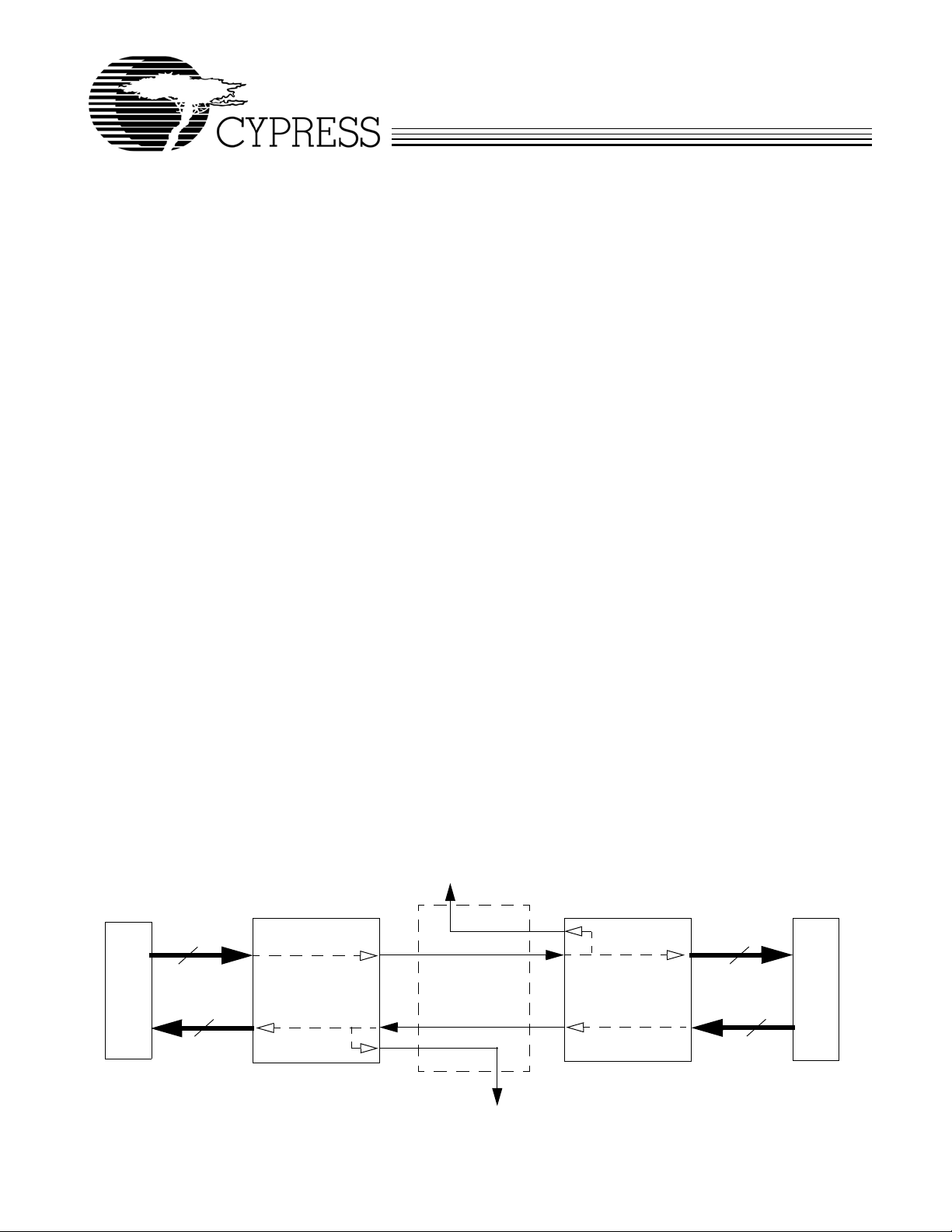
retransmitted through the reclocker serial outputs. Figure 1
illustrates typical connections between independent video coprocessors and corresponding CYV15G0104TRB chips.
The CYV15G0104TRB satisfies the SMPTE 259M and
SMPTE 292M compliance as per SMPTE EG34-1999 Pathological Test Requirements.
As a second-generation HOTLink device, the
CYV15G0104TRB extends the HOTLink family with enhanced
levels of integration and faster data rates, while maintaining
serial-link compatibility (data and BIST) with other HOTLink
devices. The transmit (TX) channel of the CYV15G0104TRB
HOTLink II device accepts scrambled 10-bit transmission
characters. These characters are serialized and output from
dual Positive ECL (PECL) compatible differential transmission-line drivers at a bit-rate of either 10- or 20-times the
input reference clock for that channel.
The receive (RX) channel of the CYV15G0104TRB HOTLink
II device accepts a serial bit-stream from one of two selectable
PECL-compatible differential line receivers, and using a
completely integrated Clock and Data Recovery PLL, recovers
the timing information necessary for data reconstruction. The
recovered bit-stream is reclocked and retransmitted through
the reclocker serial outputs. Also, the recovered serial data is
deserialized and presented to the destination host system.
The transmit and receive channels contain an independent
BIST pattern generator and checker, respectively. This BIST
hardware allows at-speed testing of the high-speed serial data
paths in each transmit and receive section, and across the
interconnecting links.
Reclocked
Output
Video Coprocessor
10
10
Independent
CYV15G0104TRB
Channel
Device
Serial
Links
Reclocked
Output
Independent
Channel
CYV15G0104TRB
Device
10
10
Video Coprocessor
Figure 1. HOTLink II™ System Connections
Cypress Semiconductor Corporation • 3901 North First Street • San Jose, CA 95134 • 408-943-2600
Document #: 38-02100 Rev. *B Revised July 8, 2005
[+] Feedback
Page 2
CYV15G0104TRB
The CYV15G0104TRB is ideal for SMPTE applications where
different data rates and serial interface standards are
necessary for each channel. Some applications include multi-
format routers, switchers, format converters, SDI monitors,
cameras, and camera control units.
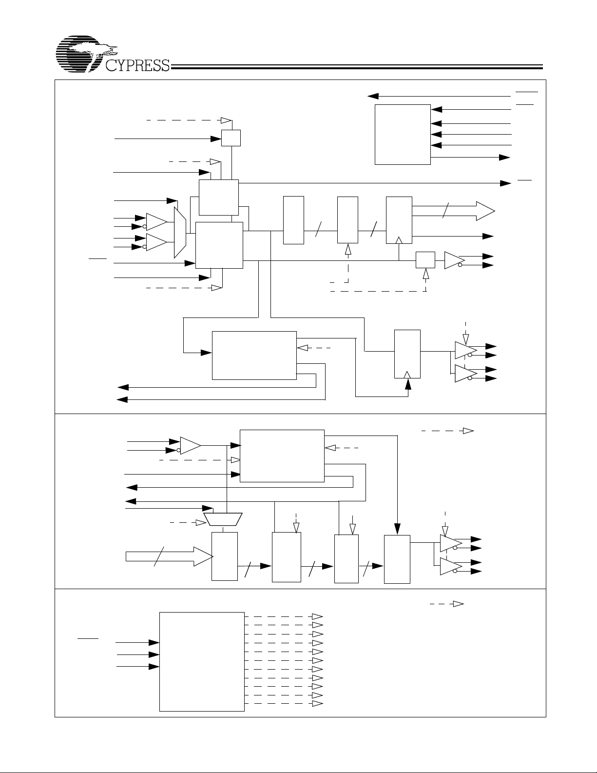
CYV15G0104TRB Serializer and Reclocking Deserializer Logic Block Diagram
TXDB[9:0]
REFCLKB±
Deserializer
Reclocker
x10
RXDA[9:0]
RX
TRGCLKA±
x10
Phase
Align
Buffer
Serializer
TX
INA1±
INA2±
TOUTB1±
ROUTA1±
ROUTA2±
TOUTB2±
Document #: 38-02100 Rev. *B Page 2 of 27
[+] Feedback
Page 3
CYV15G0104TRB
Reclocking Deserializer Path Block Diagram
TRGRATEA
TRGCLKA
SDASEL[2..1]A[1:0]
LDTDEN
INSELA
INA1+
INA1–
INA2+
INA2–
ULCA
SPDSELA
RXPLLPDA
Recovered Character Clock
RECLKOA
REPDOA
x2
Receive
Signal
Monitor
Clock &
Data
Recovery
PLL
Recovered Serial Data
Reclocker
Output PLL
Clock Multiplier
Character-Rate Clock
10
Shifter
RXBISTA[1:0]
RXRATEA
ROE[2..1]A
Boundary
Controller
10
BIST LFSR
Bit-Rate Clock
JTAG
Scan
Output
Register
Register
÷2
10
ROE[2..1]A
RESET
TRST
TMS
TCLK
TDI
TDO
LFIA
RXDA[9:0]
BISTSTA
RXCLKA+
RXCLKA–
ROUTA1+
ROUTA1–
ROUTA2+
ROUTA2–
Serializer Path Block Diagram
REFCLKB+
REFCLKB–
SPDSELB
TXCLKOB
TXERRB
TXCLKB
TXDB[9:0]
TXRATEB
TXCKSELB
10
10
Input
Transmit PLL
Transmit PLL
Clock Multiplier
Clock Multiplier
Character-Rate Clock
10
Register
PABRSTB
Buffer
Buffer
Phase-Align
Phase-Align
Device Configuration and Control Block Diagram
WREN
ADDR[2:0]
DATA[6:0]
Device Configuration
and Control Interface
Bit-Rate Clock
TOE[2..1]B
TXBISTB
10
BIST LFSR
RXRATEA
RXPLLPDA
TRGRATEA
TXRATEB
TXCKSELB
PABRSTB
SDASEL[2..1]A[1:0]
TOE[2..1]B
ROE[2..1]A
RXBISTA[1:0]
TXBISTB
10
Shifter
= Internal Signal
TOE[2..1]B
TOUTB1+
TOUTB1–
TOUTB2+
TOUTB2–
= Internal Signal
Document #: 38-02100 Rev. *B Page 3 of 27
[+] Feedback
Page 4

CYV15G0104TRB
Pin Configuration (Top View)
[1]
1 2 3 4 5 6 7 8 9 10 11 12 13 14 15 16 17 18 19 20
A
NC NC NC NC V
B
VCCNC V
C
TDI TMS
D
TCLK RESET
E
VCCVCCVCCV
F
NC NC V
G
H
J
WREN
GND
GND GND GND GND GND GND GND GND
GND GND GND GND NC NC NC NC
CC
VCCVCCV
INSELA
V
CC
CC
GND GND NC NC
CC
NC VCCV
CC
V
CC
CC
NC V
TOUT
NC
CC
B1–
TOUT
B1+
GND GND
GND NC
NC NC GND
ULCA
NC GND
DATA
[6]
DATA
[5]
TOUT
B2–INA1–
TOUT
B2+INA1+
DATA
[4]
DATA
[3]
ROUT
GND
A1–
ROUT
GND
A1+
DATA
DATA
[2]
DATA
[1]
GND NC
[0]
GND GND GND NC V
IN
A2–
IN
A2+
ROUT
A2–
ROUT
A2+
SPD
SELB
VCCV
CC
V
NC NC NC NC
CC
LDTD ENTRST
V
CC
NC V
CC
VCCVCCVCCV
CC
NC V
CC
CC
GND
SCAN
EN2
NC
TDO
TMEN3
NC NC NC
SPD
NC
SELA
CC
K
NC NC GND GND NC NC NC NC
L
NC NC NC GND NC NC NC GND
M
NC NC NC NC NC NC NC GND
N
GND GND GND GND GND GND GND GND
P
NC NC NC NC GND GND GND GND
R
NC NC NC NC VCCVCCVCCV
T
VCCVCCVCCV
U
TX
DB[0]TXDB[1]TXDB[2]TXDB[9]
V
TX
DB[3]TXDB[4]TXDB[8]
W
TX
DB[5]TXDB[7]
Y
TX
DB[6]TXCLKB
CC
NC V
NC NC V
NC NC V
V
NC NC GND GND
CC
NC NC GND NC GND
CC
NC NC GND
CC
NC NC GND
CC
ADDR
[2]
TX
CLKOB
ADDR
[0]
CLKB–
CLKB+RECLKOA
ADDR
[1]RXCLKA+
NC GND
REF
GND GND GND VCCV
REF
GND GND VCCV
REPDO
GND GND VCCV
A
RX
GND GND VCCV
CLKA–
VCCVCCVCCV
RX
CC
CC
CC
CC
V
DA[4]
DA[9]RXDA[5]RXDA[2]RXDA[1]
ERRB
CC
RX
LFIA TRG
CLKA+RXDA[6]RXDA[3]
TX
TRG
CLKA–RXDA[8]RXDA[7]
BIST
STARXDA[0]
CC
CC
Note:
1. NC = Do not connect.
Document #: 38-02100 Rev. *B Page 4 of 27
[+] Feedback
Page 5

CYV15G0104TRB
Pin Configuration (Bottom View)
[1]
20 19 18 17 16 15 14 13 12 11 10 9 8 7 6 5 4 3 2 1
A
NC V
B
NC NC NC NC V
C
TDO
D
TMEN3 SCAN
E
VCCVCCVCCV
F
NC NC NC V
G
NC
H
GND GND GND GND GND GND GND GND
J
NC NC NC NC GND GND GND GND
NC VCCV
CC
TRST LDTD
GND
EN2
SPD
SELA
EN
V
NC V
CC
CC
CC
NC NC GND GND
ROUT
CC
A2–INA2–
ROUT
CC
A2+INA2+
SPD
V
CC
CC
NC GND
SELB
NC GND GND GND
GND
GND
ROUT
A1–INA1–
ROUT
A1+INA1+
DATA
[0]
DATA
[2]
DATA
[1]
TOUT
B2–
TOUT
B2+
DATA
[4]
DATA
[3]
GND GND
NC GND
DATA
[6]
DATA
[5]
TOUT
NC V
B1–
TOUT
VCCV
B1+
GND NC NC VCCVCCV
GND NC
ULCA
NC NC NC NC
CC
NC V
CC
INSELA
V
CC
VCCVCCVCCV
NC V
CC
CC
V
CC
CC
NC V
CC
TMS TDI
RESET TCLK
CC
NC NC
WREN
GND
K
NC NC NC NC GND GND NC NC
L
GNDNCNCNC GND NC NC NC
M
GNDNCNCNC NC NC NC NC
N
GND GND GND GND GND GND GND GND
P
GND GND GND GND NC NC NC NC
R
VCCVCCVCCV
T
VCCVCCVCCV
U
RX
BIST
DA[0]
STA
V
RX
DA[1]RXDA[2]RXDA[5]RXDA[9]
W
RX
DA[3]RXDA[6]
Y
RX
DA[7]RXDA[8]
CC
CC
RX
V
CC
DA[4]
TRG
LFIA
CLKA+
TRG
CLKA–TXERRB
VCCVCCGND GND GND
VCCVCCGND GND
VCCVCCGND GND
VCCVCCGND GND
RE
CLKOA
REPDOARX
RX
CLKA–
REF
ADDR
CLKB–
REF
CLKB+
CLKA+
GND NC
GND GND NC NC V
[0]
GND NC GND NC NC V
ADDR
ADDR
[1]
GND NC NC V
[2]
TX
GND NC NC V
CLKOB
NC NC NC NC
VCCVCCVCCV
TX
CC
DB[9]TXDB[2]TXDB[1]TXDB[0]
TX
NC
CC
CC
CC
DB[8]TXDB[4]TXDB[3]
NC NC
NC NC
CC
TX
DB[7]TXDB[5]
TX
CLKBTXDB[6]
Document #: 38-02100 Rev. *B Page 5 of 27
[+] Feedback
Page 6

CYV15G0104TRB
Pin Definitions
CYV15G0104TRB HOTLink II Serializer and Reclocking Deserializer
Name I/O Characteristics Signal Description
Transmit Path Data and Status Signals
TXDB[9:0] LVTTL Input,
synchronous,
sampled by
TXCLKB↑ or
REFCLKB↑
[2]
TXERRB LVTTL Output,
synchronous to
REFCLKB↑
[3]
,
asynchronous to
transmit channel
enable / disable,
asynchronous to loss
or return of
REFCLKB±
Transmit Path Clock Signals
REFCLKB± Differential LVPECL
or single-ended
LVTTL input clock
TXCLKB LVTTL Clock Input,
internal pull-down
TXCLKOB LVTTL Output Transmit Clock Output. TXCLKOB output clock is synthesized by the transmit PLL and
Receive Path Data and Status Signals
RXDA[9:0] LVTTL Output,
synchronous to the
RXCLKA ± output
Notes:
2. When REFCLKB± is configured for half-rate operation, these inputs are sampled relative to both the rising and falling edges of the associated RE FCLKB±.
3. When REFCLKB± is configured for half-rate operation, this output is presented relative to both the rising and falling edges of the associated REFCLKB±.
Trans mit D ata In puts. TXDB[9:0] data inputs are captured on the risin g edge of the
transmit interface clock. The transmit interface clock is selected by the TXCKSELB latch
via the device configuration interface.
Transmit Path Error. TXERRB is asserted HIGH to indicate detection of a transmit
Phase-Align Buffer underflow or overflow. If an underflow or overflow condition is
detected, TXERRB, is asserted HIGH and remains asserted until the transmit Phase-Align
Buffer is re-centered with the PABRSTB latch via the device configuration interface. When
TXBISTB = 0, the BIST progress is presented on the TXERRB output. The TXERRB
signal pulses HIGH for one transmit-character clock period to indicate a pass through the
BIST sequence once every 511 character times.
TXERRB is also asserted HIGH, when any of the following conditions is true:
• The TXPLL is powered down. This occurs when TOE2B and TOE1B are both disabled
by setting TOE2B = 0 and TOE1B = 0.
• The absence of the REFCLKB± signal.
Reference Clock. REFCLKB± clock inputs are used as the timing reference for the
transmit PLL. This input clock may also be selected to clock the transmit parallel interface.
When driven by a single-ended LVCMOS or L VTTL clock source, connect the clock source
to either the true or complement REFCLKB input, and leave the alternate REFCLKB input
open (floating). When driven by an LVPECL clock source, the clock must be a differential
clock, using both inputs.
Transmit Path Input Clock. When configuration latch TXCKSELB = 0, the associated
TXCLKB input is selected as the character-rate input clock for the TXDB[9:0] input. In this
mode, the TXCLKB input must be frequency-coherent to its TXCLKOB output clock, but
may be offset in phase by any amount. Once initialized, TXCLKB is allowed to drift in
phase by as much as ±180 degrees. If the input phase of TXCLKB drifts beyond the
handling capacity of the Phase Align Buffer, TXERRB is asserted to indicate the loss of
data, and remains asserted until the Phase Align Buffer is initialized. The phase of
TXCLKB relative to REFCLKB± is initialized when the configuration latch PABRSTB is
written as 0. When TXERRB is deasserted, the Phase Align Buffer is initialized and input
characters are correctly captured.
operates synchronous to the internal transmit character clock. TXCLKOB operates at
either the same frequency as REFCLKB± (TXRATEB = 0), or at twice the frequency of
REFCLKB± (TXRATEB = 1). The transmit clock outputs have no fixed phase relationship
to REFCLKB±.
Parallel Data Output. RXDA[9:0] parallel data outputs change relative to the receive
interface clock. If RXCLKA± is a full-rate clock, the RXCLKA± clock outputs are complementary clocks operating at the character rate. The RXDA[9:0] outputs for the associated
receive channels follow rising edge of RXCLKA+ or falling edge of RXCLKA–. If RXCLKA±
is a half-rate clock, the RXCLKA± clock outputs are complementary clocks operating at
half the character rate. The RXDA[9:0] outputs for the associated receive channels follow
both the falling and rising edges of the associated RXCLKA± clock outputs.
When BIST is enabled on the receive channel, the BIST status is presented on the
RXDA[1:0] and BISTSTA outputs. See Table 6 for each status reported by the BIST state
machine. Also, while BIST is enabled, the RXDA[9:2] outputs should be ignored.
Document #: 38-02100 Rev. *B Page 6 of 27
[+] Feedback
Page 7

CYV15G0104TRB
Pin Definitions (continued)
CYV15G0104TRB HOTLink II Serializer and Reclocking Deserializer
Name I/O Characteristics Signal Description
BISTSTA LVTTL Output,
synchronous to the
RXCLKA ± output
REPDOA Asynchronous to
reclocker output
channel
enable/disable
Receive Path Clock Signals
TRGCLKA± Differential LVPECL
or single-ended
LVTTL input clock
RXCLKA± LVTTL Output Clock Receive Clock Output. RXCLKA± is the receive interface clock used to control timing of
RECLKOA LVTTL Output Reclocker Clock Output. RECLKOA output clock is synthesized by the reclocker output
Device Control Signals
RESET
LDTDEN LVTTL Input,
ULCA
LVTTL Input,
asynchronous,
internal pull-up
internal pull-up
LVTTL Input,
internal pull-up
BIST Status Output. When RXBISTA[1:0] = 10, BISTSTA (along with RXDA[1:0])
displays the status of the BIST reception. See Table 6 for the BIST status reported for
each combination of BISTSTA and RXDA[1:0].
When RXBISTA[1:0] ≠ 10, BISTSTA should be ignored.
Reclocker Powered Down Status Output. REPDOA is asserted HIGH, when the
reclocker output logic is powered down. This occurs when ROE2A and ROE1A are both
disabled by setting ROE2A = 0 and ROE1A = 0.
CDR PLL Training Clock. TRGCLKA± clock inputs are used as the reference source for
the frequency detector (Range Controller) of the receive PLL to reduce PLL acquisition
time.
In the presence of valid serial data, the recovered clock output of the receive CDR PLL
(RXCLKA±) has no frequency or phase relationship with TRGCLKA±.
When driven by a single-ended LVCMOS or L VTTL clock source, connect the clock source
to either the true or complement TRGCLKA input, and leave the alternate TRGCLKA input
open (floating). When driven by an LVPECL clock source, the clock must be a differential
clock, using both inputs.
the RXDA[9:0] parallel outputs. These true and complement clocks are used to control
timing of data output transfers. These clocks are output continuously at either the halfcharacter rate (1/20
data being received, as selected by RXRATEA.
PLL and operates synchronous to the internal recovered character clock. RECLKOA
operates at either the same frequency as RXCLKA± (RXRATEA = 0), or at twice the
frequency of RXCLKA± (RXRATEA = 1).The reclocker clock outputs have no fixed phase
relationship to RXCLKA±.
Asynchronous Device Reset. RESET
configuration latches in the device to a known state. RESET
minimum pulse width. When the reset is removed, all state machines, counters and configuration latches are at an initial state. See Table 4 for the initialize values of the device
configuration latches.
Level Detect Transition Density Enable. When LDTDEN is HIGH, the Signal Level
Detector, Range Controller, and Transition Density Detector are all enabled to determine
if the RXPLL tracks TRGCLKA± or the selected input serial data stream. If the Signal Level
Detector, Range Controller , or Transition Density Detector are out of their respective limits
while LDTDEN is HIGH, the RXPLL locks to TRGCLKA± until such a time they become
valid. SDASEL[2..1]A[1:0] is used to configure the trip level of the Signal Level Detector.
The Transition Density Detector limit is one transition in every 60 consecutive bits. When
LDTDEN is LOW, only the Range Controller is used to determine if the RXPLL tracks
TRGCLKA± or the selected input serial data stream. it is recommended to set LDTDEN
= HIGH.
Use Local Clock. When ULCA is LOW, the RXPLL is forced to lock to TRGCLKA± instead
of the received serial data stream. While ULCA
LOW indicating a link fault.
When ULCA
input data streams. This function is used in applications in which a stable RXCLKA± is
needed. In cases when there is an absence of valid data transitions for a long period of
time, or the high-gain differential serial inputs (INA±) are left floating, there may be brief
frequency excursions of the RXCLKA± outputs from TRGCLKA±.
th
the serial bit-rate) or character rate (1/10th the serial bit-rate) of the
initializes all state machines, counters, and
must be asserted LOW for a
is LOW, the link fault indicator LFIA is
is HIGH, the RXPLL performs Clock and Data Recovery functions on the
Document #: 38-02100 Rev. *B Page 7 of 27
[+] Feedback
Page 8
CYV15G0104TRB
Pin Definitions (continued)
CYV15G0104TRB HOTLink II Serializer and Reclocking Deserializer
Name I/O Characteristics Signal Description
SPDSELA
SPDSELB
3-Level Select
static control input
INSELA LVTTL Input,
asynchronous
LFIA
LVTTL Output,
asynchronous
Device Configuration and Control Bus Signals
WREN LVTTL input,
asynchronous,
internal pull-up
ADDR[2:0] LVTTL input
asynchronous,
internal pull-up
DATA[6:0] LVTTL input
asynchronous,
internal pull-up
Internal Device Configuration Latches
RXRATEA Internal Latch
SDASEL[2..1]
Internal Latch
A[1:0]
TXCKSELB Internal Latch
TXRATEB Internal Latch
TRGRATEA Internal Latch
RXPLLPDA Internal Latch
RXBISTA[1:0] Internal Latch
TXBISTB Internal Latch
TOE2B Internal Latch
TOE1B Internal Latch
Notes:
4. 3-Level Select inputs are used for stati c configuration. These are terna ry inputs tha t make use of logic levels of LOW , MI D, and HIGH. The LOW level is usually
implemented by direct connection to V
implemented by not connecting the input (left floating), whi ch allows it to self bias to the proper level.
5. See Device Configuration and Control Interface for detailed informa tion on the operation of the Configuration Interface.
6. See Device Configuration and Control Interface for detailed informa tion on the internal latches.
[4]
Serial Rate Select. The SPDSELA and SPDSELB inputs specify the operating signalingrate range of the receive and transmit PLL, respectively.
LOW = 195 – 400 MBd
MID = 400 – 800 MBd
HIGH = 800 – 1500 MBd.
Receive Input Selector. The INSELA in put determines which external serial bit stream
is passed to the receiver’s Clock and Data Recovery circuit. When INSELA is HIGH, the
Primary Differential Serial Data Input, INA1±, is selected for the receive channel. When
INSELA is LOW, the Secondary Differential Serial Data Input, INA2±, is selected for the
receive channel.
Link Fault Indication Output. LFIA is an output status indicator signal. LFIA is the logical
OR of six internal conditions. LFIA
is asserted LOW when any of the following conditions
is true:
• Received serial data rate outside expected range
• Analog ampl itude below expected levels
• Transition density lower than expected
• Receive channel disabled
•ULCA
is LOW
• Absence of TRGCL KA±.
Control Write Enable. The WREN input writes the values of the DATA[6:0] bus into the
latch specified by the address location on the ADDR[2:0] bus.
[5]
Control Addressing Bus. The ADDR[2:0] bus is the input address bus used to configure
the device. The WREN input writes the values of the DAT A[6:0] bus into the latch specified
by the address location on the ADDR[2:0] bus.
[5]
Table 4 lists the configuration latches
within the device, and the initialization value of the latches upon the assertion of RESET
Table 5 shows how the latches are mapped in the device.
Control Data Bus. The DA TA[6:0] bus is the input data bus used to configure the device.
The WREN
location on the ADDR[2:0] bus.
and the initialization value of the latches upon the assertion of RESET
input writes the values of the DAT A[6:0] bus into the latch specified by address
[5 ]
Table 4 lists the configuration latches within the device,
. Table 5 shows how
the latches are mapped in the device.
[6]
[6]
[6]
[6]
[6]
[6]
[6]
[6]
[6]
[6]
Receive Clock Rate Select.
Signal Detect Amplitude Select.
Transmit Clock Select.
Transmit PLL Clock Rate Select.
Reclocker Output PLL Clock Rate Select.
Receive Channel Power Control.
Receive Bist Disabled.
Transmit Bist Disabled.
Transmitter Differential Serial Output Driver 2 Enable.
Transmitter Differential Serial Output Driver 1 Enable.
(ground). The HIGH level is usually implemented by direct connection to VCC (power). The MID level is usually
SS
.
Document #: 38-02100 Rev. *B Page 8 of 27
[+] Feedback
Page 9
CYV15G0104TRB
Pin Definitions (continued)
CYV15G0104TRB HOTLink II Serializer and Reclocking Deserializer
Name I/O Characteristics Signal Description
ROE2A Internal Latch
ROE1A Internal Latch
PABRSTB Internal Latch
Factory Test Modes
SCANEN2 LVTTL input,
TMEN3 LVTTL input,
Analog I/O
TOUTB1± CML Differential
TOUTB2± CML Differential
ROUTA1± CML Differential
ROUTA2± CML Differential
INA1± Differential Input Primary Differential Serial Data Input. The INA1± input accepts the serial data stream
INA2± Differential Input Secondary Differential Serial Data Input. The INA2± input accepts the serial data
JTAG Interface
TMS LVTTL Input,
TCLK LVTTL Input,
TDO 3-State LVTTL Output Test Data Out. JTAG data output buffer. High-Z while JTAG test mode is not selected.
TDI LVTTL Input,
TRST
Power
V
CC
GND Signal and Power Ground for all internal circuits.
internal pull-down
internal pull-down
Output
Output
Output
Output
internal pull-up
internal pull-down
internal pull-up
LVTTL Input,
internal pull-up
[6]
[6]
[6]
Reclocker Differential Serial Output Driver 2 Enable.
Reclocker Differential Serial Output Driver 1 Enable.
Transmit Clock Phase Alignment Buffer Reset.
Factory Test 2. SCANEN2 input is for factory testing only . This input may be left as a NO
CONNECT, or GND only.
Factory Test 3. TMEN3 input is for factory testing only. This input may be left as a NO
CONNECT, or GND only.
Transmitter Primary Differential Serial Data Outpu t. The transmitter TOUTB 1± PECLcompatible CML outputs (+3.3V referenced) are capable of driving terminated transmission lines or standard fiber-optic transmitter modules, and must be AC-coupled for
PECL-compatible connections.
Transmitter Secondary Differential Serial Data Output. T he transmitter TOUTB2± PE CLcompatible CML outputs (+3.3V referenced) are capable of driving terminated transmission lines
or standard fiber-optic transmitter modules, and must be AC-coupled for PECL-compatible
connections.
Reclocker Primary Differential Serial Data Output. The reclocker ROUTA1± PECLcompatible CML outputs (+3.3V referenced) are capable of driving terminated transmission lines or standard fiber-optic transmitter modules, and must be AC-coupled for
PECL-compatible connections.
Rec loc ker Secondary Differential Serial Data Output. The reclocker ROUTA2± PECLcompatible CML outputs (+3.3V referenced) are capable of driving terminated transmission lines
or standard fiber-optic transmitter modules, and must be AC-coupled for PECL-compatible
connections.
for deserialization. The INA1± serial stream is passed to the receive CDR circuit to extract
the data content when INSELA = HIGH.
stream for deserialization. The INA2± serial stream is passed to the receiver CDR circuit
to extract the data content when INSELA = LOW.
Test Mode Select. Used to control access to the JT AG Test Modes. If maintained high for
≥5 TCLK cycles, the JTAG test controller is reset.
JTAG Test Clock.
Test Data In. JTAG data input port.
JTAG reset signal. When asserted (LOW), this input asynchronously resets the JTAG
test access port controller.
+3.3V Power.
CYV15G0104TRB HOTLink II Operation
The CYV15G0104TRB is a highly configurable, independent
clocking device designed to support reliable transfer of large
quantities of digital video data, using high-speed serial links
from multiple sources to multiple destinations.
Document #: 38-02100 Rev. *B Page 9 of 27
CYV15G0104TRB Transmit Data Path
Input Register
The parallel input bus TXDB[9:0] can be clocked in using
TXCLKB (TXCKSELB = 0) or REFCLKB (TXCKSELB = 1).
[+] Feedback
Page 10

CYV15G0104TRB
Phase-Align Buffer
Data from the Input Register is passed to the Phase-Align
Buffer, when the TXDB[9:0] input register is clocked using
TXCLKBA (TXCKSELB = 0) or when REFCLKB is a half-rate
clock (TXCKSELB = 1 and TXRATEB = 1). When the
TXDB[9:0] input register is clocked using REFCLKB±
(TXCKSELA = 1) and REFCLKB± is a full-rate clock
(TXRATEB = 0), the associated Phase Alignment Buffer in the
transmit path is bypassed. These buffers are used to absorb
clock phase differences between the TXCLKB input clock and
the internal character clock for that channel.
Once initialized, TXCLKB is allowed to drift in phase as much
as ±180 degrees. If the input phase of TXCLKB drifts beyond
the handling capacity of the Phase Align Buffer, TXERRB is
asserted to indicate the loss of data, and remains asserted
until the Phase Align Buffer is initialized. The phase of
TXCLKB relative to its internal character rate clock is initialized
when the configuration latch PABRSTB is written as 0. When
the associated TXERRB is deasserted, the Phase Align Buffer
is initialized and input characters are correctly captured.
If the phase offset, between the initialized location of the input
clock and REFCLKB, exceeds the skew handling capabilities
of the Phase-Align Buffer, an error is reported on that
channel’s TXERRB output. This output indicates an error
continuously until the Phase-Align Buffer for that channel is
reset. While the error remains active, the transmitter for that
channel outputs a continuous “1001111000” character to
indicate to the remote receiver that an error condition is
present in the link.
Transmit BIST
The transmit channel contains an internal pattern generator
that can be used to validate both the link and device operation.
This generator is enabled by the TXBISTB latch via the device
configuration interface. When enabled, a register in the
transmit channel becomes a signature pattern generator by
logically converting to a Linear Feedback Shift Register
(LFSR). This LFSR generates a 511-character sequence. This
provides a predictable yet pseudo-random sequence that can
be matched to an identical LFSR in the attached Receiver(s).
A device reset (RESET
sampled LOW) presets the BIST
Enable Latches to disable BIST on all channels.
All data present at the TXDB[9:0] inputs are ignored when
BIST is active on that channel.
Transmit PLL Clock Multiplier
The Transmit PLL Clock Multiplier accepts a character-rate or
half-character-rate external clock at the REFCLKB± input, and
that clock is multiplied by 10 or 20 (as selected by TXRATEB)
to generate a bit-rate clock for use by the transmit shifter. It
also provides a character-rate clock used by the transmit
paths, and outputs this character rate clock as TXCLKOB.
The clock multiplier PLL can accept a REFCLKB± input
between 19.5 MHz and 150 MHz, however, this clock range is
limited by the operating mode of the CYV15G0104TRB cloc k
multiplier (TXRATEB) and by the level on the SPDSELB input.
SPDSELB is a 3-level select
[4]
input that selects one of three
operating ranges for the serial data outputs of the transmit
channel. The operating serial signaling-rate and allowable
range of REFCLKB± frequencies are listed in Table 1.
Table 1. Operating Speed Settings
REFCLKB±
SPDSELB TXRATEB
LOW
1 reserved 195–400
Frequency
(MHz)
Signaling
Rate (Mbps)
0 19.5–40
MID (Open) 1 20–40 400–800
0 40–80
HIGH 1 40–75 800–1500
0 80–150
The REFCLKB± inputs are differential inputs with each input
internally biased to 1.4V. If the REFCLKB+ input is connected
to a TTL, LVTTL, or LVCMOS clock source, the input signal is
recognized when it passes through the internally biased
reference point. When driven by a single-ended TTL, LVTTL,
or LVCMOS clock source, connect the clock source to either
the true or complement REFCLKB input, and leave the
alternate REFCLKB input open (floating).
When both the REFCLKB+ and REFCLKB– inputs are
connected, the clock source must be a differential clock. Thi s
can either be a differential LVPECL clock that is DC-or
AC-coupled or a differential LVTTL or LVCMOS clock.
By connecting the REFCLKB– input to an external voltage
source, it is possible to adjust the reference point of the
REFCLKB+ input for alternate logic levels. When doing so, it
is necessary to ensure that the input differential crossing point
remains within the parametric range supported by the input.
Transmit Serial Output Drivers
The serial output interface drivers use differential Current
Mode Logic (CML) drivers to provide source-matched drivers
for 50Ω transmission lines. These drivers accept data from the
transmit shifter. These drivers have signal swings equivalent
to that of standard PECL drivers, and are capable of driving
AC-coupled optical modules or transmission lines.
Transmit Channels Enabled
Each driver can be enabled or disabled separately via the
device configuration interface.
When a driver is disabled via the configuration interface, it is
internally powered down to reduce device power. If both
transmit serial drivers are in this disabled state, the transmitter
internal logic for that channel is also powered down. A device
reset (RESET
sampled LOW) disables all output drivers.
Note. When the disabled transmit channel (i.e., both outputs
disabled) is re-enabled:
• the data on the transmit serial outputs may not meet all
timing specifications for up to 250 µs
• the state of the phase-align buffer cannot be guaranteed,
and a phase-align reset is required if the phase-align buffer
is used
CYV15G0104TRB Receive Data Path
Serial Line Receivers
Two differential Line Receivers, INA1± and INA2±, are
available on the receive channel for accepting serial data
streams. The active Serial Line Receiver is selected using the
Document #: 38-02100 Rev. *B Page 10 of 27
[+] Feedback
Page 11

CYV15G0104TRB
INSELA input. The Serial Line Receiver inputs are differential,
and can accommodate wire interconnect and filtering losses
or transmission line attenuation greater than 16 dB. For
normal operation, these inputs should receive a signal of at
least VI
Each Line Receiver can be DC- or AC-coupled to +3.3V
> 100 mV, or 200 mV peak-to-peak differential.
DIFF
powered fiber-optic interface mo dule s (any ECL /PEC L fam ily,
not limited to 100K PECL) or AC-coupled to +5V powered
optical modules. The common-mode tolerance of these line
receivers accommodates a wide range of signal termination
voltages. Each receiver provides internal DC-restoration, to
the center of the receiver’s common mode range, for ACcoupled signals.
Signal Detect/Link Fault
Each selected Line Receiver (i.e., that routed to the clock and
data recovery PLL) is simultaneously monitored for
• analog amplitude above amplitude level selected by
SDASELA
• transitio n density above the specified limit
• range controls rep ort the received data stream inside
normal frequency range (±1500 ppm
[24]
)
• receive channel enabled
• Presence of reference clock
•ULCA
is not asserted.
All of these conditions must be valid for the Signal Detect block
to indicate a valid signal is present. This status is presented on
the LFIA
(Link Fault Indicator) output associated with each
receive channel, which changes synchronous to the receive
interface clock.
Analog Amplitude
While most signal monitors are based on fixed constants, the
analog amplitude level detection is adjustable to allow
operation with highly attenuated signals, or in high-noise
environments. The analog amplitude level detection is set by
the SDASELA latch via device configuration interface. The
SDASELA latch sets the trip point for the detection of a valid
signal at one of three levels, as listed in Table 2. This control
input affects the analog monitors for all receive channels. The
Analog Signal Detect monitors are active for the Line Receiver
as selected by the INSELA input.
Table 2. Analog Amplitude Detect Valid Signal Levels
[7]
Typical Signal with Peak Amplitudes
SDASELA
Above
00 Analog Signal Detector is disabled
01 140 mV p-p differential
10 280 mV p-p differential
11 420 mV p-p differential
Transition Density
The Transition Detection logic checks for the absence of
transitions spanning greater than six transmission characters
(60 bits). If no transitions are present in the data received, the
Detection logic for that channel asserts LFIA
.
Range Controls
The CDR circuit includes logic to monitor the frequency of the
PLL Voltage Controlled Oscillator (VCO) used to sample the
incoming data stream. This logic ensures that the VCO
operates at, or near the rate of the incoming data stream for
two primary cases:
• w hen the incoming data stream resumes after a time in
which it has been “missing.”
• w hen the incoming data stream is outside the acceptable
signaling rate range.
To perform this function, the frequ ency of the RXPLL VCO is
periodically compared to the frequency of the TRGCLKA±
input. If the VCO is running at a frequency beyond
±1500ppm
[24]
as defined by the TRGCLKA± frequency, it is
periodically forced to the correct frequency (as defined by
TRGCLKA±, SPDSELA, and TRGRATEA) and then released
in an attempt to lock to the input data stream.
The sampling and relock period of the Range Control is calculated as follows: RANGE_CONTROL_ SAMPLING_PERIOD
= (RECOVERED BYTE CLOCK PERIOD) * (4096).
During the time that the Range Control forces the RXPLL VCO
to track TRGCLKA±, the LFIA
output is asserted LOW. Af ter a
valid serial data stream is applied, it may take up to one
RANGE CONTROL SAMPLING PERIOD before the PLL
locks to the input data stream, after which LFIA
should be
HIGH.
The operating serial signaling-rate and allowable range of
TRGCLKA± frequencies are listed in Table 3.
Table 3. Operating Speed Settings
TRGCLKA±
SPDSELA TRGRATEA
LOW
1 reserved 195–400
Frequency
(MHz)
Signaling
Rate (Mbps)
0 19.5–40
MID (Open) 1 20–40 400–800
0 40–80
HIGH 1 40–75 800–1500
0 80–150
Receive Channel Enabled
The receive channel can be enabled or disabled through the
RXPLLPDA input latch as controlled by the device configuration interface. When RXPLLPDA = 0, the CDR PLL and
analog circuitry of the channel are disabled. Any disabled
channel indicates a constant link fault condition on the LFIA
output. When RXPLLPDA = 1, the CDR PLL and receive
channel are enabled to receive a serial stream.
Note. When the disabled receive channel is reenabled, the
status of the LFIA
output and data on the parallel outputs for
the associated channel may be indeterminate for up to 2 ms.
Clock/Data Recovery
The extraction of a bit-rate clock and recovery of bits from the
received serial stream is performed by a separate CDR block
within the receive channel. The clock extraction function is
Note:
7. The peak amplitudes listed in this table ar e for typical wavefo rms that have generally 3–4 transiti ons for every ten bit s. In a worse case environmen t the signals
may have a sine-wave appearance (highest transition density with repeating 0101...). Signal peak amplitudes levels within this environment type could increase
the values in the table above by approximately 100 mV.
Document #: 38-02100 Rev. *B Page 11 of 27
[+] Feedback
Page 12

CYV15G0104TRB
performed by an integrated PLL that tracks the frequency of
the transitions in the incoming bit stream and aligns the phase
of the internal bit-rate clock to the transitions in the selected
serial data stream.
Each CDR accepts a character-rate (bit-rate
character-rate (bit-rate
TRGCLKA± input. This TRGCLKA± input is used to
• ensure that the VCO (within the CDR) is operating at the
correct frequency (rather than a harmonic of the bit-rate)
• reduce PLL acquisition time
• limit unlocked frequency excursions of the CDR VCO when
there is no input data present at the selected Serial Line
Receiver.
Regardless of the type of signal present, the CDR attempts to
recover a data stream from it. If the signaling rate of the
recovered data stream is outside the limits set by the range
control monitors, the CDR tracks TRGCLKA± instead of the
data stream. Once the CDR output (RXCLKA±) frequency
returns back close to the TRGCLKA± frequency, the CDR
input is switched back to the input data stream. If no data is
present at the selected line receiver, this switching behavior
may result in brief RXCLKA± frequency excursions from
TRGCLKA±. However, the validity of the input data stream is
indicated by the LFIA
required to be within ±1500ppm
clock that drives the REFCLKB± input of the remote transmitter to ensure a lock to the incoming data stream. This large
ppm tolerance allows the CDR PLL to reliably receive a 1.485
or 1.485/1.001 Gbps SMPTE HD-SDI data stream with a
constant TRGCLK frequency.
For systems using multiple or redundant connections, the
LFIA
output can be used to select an alternate data stream.
When an LFIA
selection of the INA1± and INA2± input through the INSELA
input. When a port switch takes place, it is necessary for the
receive PLL for that channel to reacquire the new serial
stream.
Reclocker
The receive channel performs a reclocker function on the
incoming serial data. To do this, the Clock and Data Recovery
PLL first recovers the clock from the data. The data is retimed
by the recovered clock and then passed to an output register.
Also, the recovered character clock from the receive PLL is
passed to the reclocker output PLL which generates the bit
clock that is used to clock the retimed data into the output
register. This data stream is then transmitted through the
differential serial outputs.
Reclocker Serial Output Drivers
The serial output interface drivers use differential Current
Mode Logic (CML) drivers to provide source-matched drivers
for 50Ω transmission lines. These drivers accept data from the
reclocker output register in the reclocker channel. These
drivers have signal swings equivalent to that of standard PECL
drivers, and are capable of driving AC-coupled optical
modules or transmission lines.
Reclocker Output Channels Enabled
Each driver can be enabled or disabled separately via the
device configuration interface.
indication is detected, external logic can toggle
÷ 20) training clock from the
output. The frequency of TRGCLKA± is
[24]
of the frequency of the
÷ 10) or half-
When a driver is disabled via the configuration interface, it is
internally powered down to reduce device power. If both
reclocker serial drivers are in this disabled state, the internal
reclocker logic is also powered down. The deserialization logic
and parallel outputs will remain enabled. A device reset
(RESET
Note. When the disabled reclocker function (i.e., both outputs
disabled) is re-enabled, the data on the reclocker serial
outputs may not meet all timing specifications for up to 250 µs.
Output Bus
The receive channel presents a 10-bit data signal (and a BIST
status signal when RXBISTA[1:0] = 10).
Receive BIST Operation
The receiver channel contains an internal pattern checker that
can be used to validate both device and link operation. These
pattern checkers are enabled by the RXBISTA[1:0] latch via
the device configuration in terface. When enabled, a register in
the receive channel becomes a signatu re pattern generator
and checker by logically converting to a Linear Feedback Shift
Register (LFSR). This LFSR generates a 511-character
sequence. This provides a predictable yet pseudo-random
sequence that can be matched to an identical LFSR in the
attached Transmitter(s). When synchronized with the received
data stream, the Receiver checks each character from the
deserializer with each character generated by the LFSR and
indicates compare errors and BIST status at the RXDA[1:0]
and BISTSTA bits of the Output Register.
The BIST status bus {BISTSTA, RXDA[0], RXDA[1]} indicates
010b or 100b for one character period per BIST loop to
indicate loop completion. This status can be used to check test
pattern progress.
The specific status reported by the BIST state machine is listed
in Table 6. These same codes are reported on the receive
status outputs.
If the number of invalid characters received ever exceeds the
number of valid characters by 16, the receive BIST state
machine aborts the compare operations and resets the LFSR
to look for the start of the BIST sequence again.
A device reset (RESET
Enable Latches to disable BIST on all channels.
BIST Status State Machine
When a receive path is enabled to look for and compare the
received data stream with the BIST pattern, the {BISTSTA,
RXDA[1:0]} bits identify the present state of the BIST compare
operation.
The BIST state machine has multiple states, as shown in
Figure 2 and Table 6. When the receive PLL detects an out-oflock condition, the BIST state is forced to the Start-of-BIST
state, regardless of the present state of the BIST state
machine. If the number of detected errors ever exceeds the
number of valid matches by greater than 16, the state machine
is forced to the WAIT_FOR_BIST state where it monitors the
receive path for the first character of the next BIST sequence.
sampled LOW) disables all output drivers.
sampled LOW) presets the BIST
Power Control
The CYV15G0104TRB supports user control of the powered
up or down state of each transmit and receive channel. The
receive channels are controlled by the RXPLLPDA latch via
Document #: 38-02100 Rev. *B Page 12 of 27
[+] Feedback
Page 13

CYV15G0104TRB
the device configuration interface. When RXPLLPDA = 0, the
receive PLL and analog circuitry of the channel is disabled.
The transmit channel is controlled by the TOE1B and the
TOE2B latches via the device configuration interface. The
reclocker function is controlled by the ROE1A and the ROE2A
latches via the device configuration interface. When a driver is
disabled via the configuration interface, it is internally powered
down to reduce device power. If both serial drivers for a
channel are in this disabled state, the associated internal logic
for that channel is also powered down. When the reclocker
serial drivers are disabled, the reclocker function will be
disabled, but the deserialization logic and parallel outputs will
remain enabled.
Device Reset State
When the CYV15G0104TRB is reset by assertion of RESET
all state machines, counters, and configuration latches in the
device are initialized to a reset state. See Table 4 for the
initialize values of the configuration latches.
Following a device reset, it is necessary to enable the transmit
and receive channels used for normal operation. This can be
done by sequencing the appropriate values on the device
configuration interface.
[5]
Device Configuration and Control Interface
The CYV15G0104TRB is highly configurable via the configuration interface. The configuration interface allows the transmitter and reclocker to be configured independently. Table 4
lists the configuration latches within the device including the
Table 4. Device Configuration and Control Latch Descriptions
Name Signal Description
RXRATEA Receive Clock Rate Select. The initialization value of the RXRATEA latch = 1. RXRATEA is used to select
SDASEL1A[1:0] Primary Serial Data Input Signal Detector Amplitude Select. The initialization value of the SDASEL1A[1:0]
SDASEL2A[1:0] Secondary Serial Data Input Signal Detector Amplitude Select. The initialization value of the
TRGRATEA Training Clock Rate Select. The initialization value of the TRGRATEA latch = 0. TRGRA TEA is used to select
the rate of the RXCLKA± clock output.
When RXRATEA = 1, the RXCLKA± clock outputs are complementary clocks that follow the recovered clock
operating at half the character rate. Data for the associated receive channels should be latched alternately on
the rising edge of RXCLKA+ and RXCLKA–.
When RXRATEA = 0, the RXCLKA± clock outputs are complementary clocks that follow the recovered clock
operating at the character rate. Data for the associated receive channels should be latched on the rising edge
of RXCLKA+ or falling edge of RXCLKA–.
latch = 10. SDASEL1A[1:0] selects the trip point for the detection of a valid signal for the INA1± Primary
Differential Serial Data Inputs.
When SDASEL1A[1:0] = 00, the Analog Signal Detector is disabled.
When SDASEL1A[1:0] = 01, the typical p-p differential voltage threshold level is 140 mV.
When SDASEL1A[1:0] = 10, the typical p-p differential voltage threshold level is 280 mV.
When SDASEL1A[1:0] = 11, the typical p-p differential voltage threshold level is 420 mV.
SDASEL2A[1:0] latch = 10. SDASEL2A[1:0] selects the trip point for the detection of a valid signal for the
INA2± Secondary Differential Serial Data Inputs.
When SDASEL2A[1:0] = 00, the Analog Signal Detector is disabled
When SDASEL2A[1:0] = 01, the typical p-p differential voltage threshold level is 140 mV.
When SDASEL2A[1:0] = 10, the typical p-p differential voltage threshold level is 280 mV.
When SDASEL2A[1:0] = 11, the typical p-p differential voltage threshold level is 420 mV.
the clock multiplier for the training clock input to the CDR PLL. When TRGRATEA = 0, the TRGCLKA± input
is not multiplied before it is passed to the CDR PLL. When TRGRATEA = 1, the TRGCLKA± input is multiplied
by 2 before it is passed to the CDR PLL. TRGRATEA = 1 and SPDSELA = LOW is an invalid state and this
combination is reserved.
initialization value of the latches upon the assertion of RESET
Table 5 shows how the latches are mapped in the device.
Each row in the Table 5 maps to a 7-bit latch bank. There are
6 such write-only latch banks. When WREN
in the DATA[6:0] is latched to the latch bank specified by the
values in ADDR[2:0]. The second column of Table 5 specifies
the channels associated with the corresponding latch bank.
For example, the first three latch banks (0,1 and 2 ) consi st of
configuration bits for the reclocker channel A.
Latch Types
There are two types of latch banks: static (S) and dynamic (D).
Each channel is configured by 2 static and 1 dynamic latch
banks. The S type contain those settings that normally do not
change for a given application, whereas the D type controls
the settings that could change during the application's lifetime.
,
The first and second rows of each channel (address numbers
0, 1, 5, and 6) are the static control latches. The third row of
latches for each channel (address numbers 2 and 7) are the
dynamic control latches that are associated with enabling
dynamic functions within the device. Address numbers 3 and
4 are internal test registers.
Static Latch Values
There are some latches in the table that have a static value
(i.e. 1, 0, or X). The latches that have a ‘1’ or ‘0’ must be
configured with their corresponding value each time that their
associated latch bank is configured. The latches that have an
‘X’ are don’t cares and can be configured with any value.
= 0, the logic value
.
Document #: 38-02100 Rev. *B Page 13 of 27
[+] Feedback
Page 14

CYV15G0104TRB
Table 4. Device Configuration and Control Latch Descriptions (continued)
Name Signal Description
RXPLLPDA Receive Channel Enable. The initialization value of the RXPLLPDA latch = 0. RXPLLPDA selects if the
RXBISTA[1:0] Receive Bist Disable / SMPTE Receive Enable. The initialization value of the RXBIST A[1:0] latch = 11. For
ROE2A Reclocker Secondary Different ial Serial Data Output Driver Enable. The initialization value of the ROE2A
ROE1A Reclocker Primary Differential Serial Data Output Driver Enable. The initialization value of the ROE1A
TXCKSELB Transmit Clock Select. The initialization value of the TXCKSELB latch = 1. TXCKSELB selects the clock
TXRATEB Transmit PLL Clock Rate Select. The initialization value of the TXRATEB latch = 0. TXRATEB is used to
TXBISTB Transmit Bist Disable. The initialization value of the TXBISTB latch = 1. TXBISTB selects if the transmit BIST
TOE2B
TOE1B Primary Differential Serial Data Output Driver Enable. The initialization value of the TOE1B latch = 0.
PABRSTB Transmit Clock Phase Alignment Buffer Reset. The initialization value of the PABRSTB latch = 1. The
receive channel is enabled or powered-down. When RXPLLPDA = 0, the receive PLL and analog circuitry are
powered-down. When RXPLLPDA = 1, the receive PLL and analog circuitry are enabled.
SMPTE data reception, RXBIST A[1:0] should not remain in this initialization state (1 1). RXBISTA[1:0] selects
if receive BIST is disabled or enabled and sets the device for SMPTE data reception. When RXBISTA[1:0] =
01, the receiver BIST function is disabled and the device is set to receive SMPTE data. When RXBISTA[1:0]
= 10, the receive BIST function is enabled and the device is set to receive BIST data. RXBISTA[1:0] = 00 and
RXBIST A[1:0] = 11 are invalid states.
latch = 0. ROE2A selects if the ROUT A2± secondary differential output drivers are enabled or disabled. When
ROE2A = 1, the associated serial data output driver is enabled allowing the reclocked data to be transmitted.
When ROE2A = 0, the associated serial data output driver is disabled. When a driver is disabled via the
configuration interface, it is internally powered down to reduce device power. If both serial drivers for a channel
are in this disabled state, the reclocker logic is also powered down. A device reset (RESET sampled LOW)
disables all output drivers.
latch = 0. ROE1A selects if the ROUTA1± primary differ ential output drivers are enabled or disabled. When
ROE1A = 1, the associated serial data output driver is enabled allowing the reclocked data to be transmitted.
When ROE1A = 0, the associated serial data output driver is disabled. When a driver is disabled via the
configuration interface, it is internally powered down to reduce device power. If both serial drivers for a channel
are in this disabled state, the reclocker logic is also powered down. A device reset (RESET sampled LOW)
disables all output drivers.
source used to write data into the Transmit Input Register. When TXCKSELB = 1, the input register TXDB[9:0]
is clocked by REFCLKB↑. In this mode, the phase alignment buffer in the transmit path is bypassed. When
TXCKSELB = 0, TXCLKB↑ is used to clock in the input register TXDB[9:0].
select the clock multiplier for the Transmit PLL. When TXRATEB = 0, the transmit PLL multiples the REFCLKB±
input by 10 to generate the serial bit-rate clock. When TXRATEB = 0, the TXCLKOB output clocks are full-rate
clocks and follow the frequency and duty cycle of the REFCLKB± input. When TXRATEB = 1, the Transmit
PLL multiplies the REFCLKB± input by 20 to generate the serial bit-rate clock. When TXRATEB = 1, the
TXCLKOB output clocks are twice the frequency rate of the REFCLKB± input. When TXCKSELB = 1 and
TXRATEB = 1, the Transmit Data Inputs are captured using both the rising and falling edges of REFCLKB.
TXRATEB = 1 and SPDSELB = LOW, is an invalid state and this combination is reserved.
is disabled or enabled. When TXBISTB = 1, the transmit BIST function is disabled. When TXBISTB = 0, the
transmit BIST function is enabled.
Secondary Differential Serial Data Output Driver Enable. The initialization value of the TOE2B latch = 0.
TOE2B selects if the TOUTB2± secondary differential output drivers are enabled or disabled. When TOE2B
= 1, the associated serial data output driver is enabled allowing data to be transmitted from the transmit shifter.
When TOE2B = 0, the associated serial data output driver is disabled. When a driver is disabled via the
configuration interface, it is internally powered down to reduce device power. If both serial drivers for a channel
are in this disabled state, the associated internal logic for that channel is also powered down. A device reset
(RESET sampled LOW) disables all output drivers.
TOE1B selects if the TOUTB1± primary differential output drivers are enabled or disabled. When TOE1B = 1,
the associated serial data output driver is enabled allowing data to be transmitted from the transmit shifter.
When TOE1B = 0, the associated serial data output driver is disabled. When a driver is disabled via the
configuration interface, it is internally powered down to reduce device power. If both serial drivers for a channel
are in this disabled state, the associated internal logic for that channel is also powered down. A device reset
(RESET sampled LOW) disables all output drivers.
PABRSTB is used to re-center the Transmit Phase Align Buffer. When the configuration latch PABRSTB is
written as a 0, the phase of the TXCLKB input clock relative to REFCLKB+/- is initialized. PABRSTB is an
asynchronous input, but is sampled by each TXCLKB↑ to synchronize it to the internal clock domain.
PABRSTB is a self clearing latch. This eliminates the requirement of writing a 1 to complete the initialization
of the Phase Alignment Buffer.
Document #: 38-02100 Rev. *B Page 14 of 27
[+] Feedback
Page 15

CYV15G0104TRB
Table 5. Device Control Latch Configuration Table
ADDR Channel Type DATA6 DATA5 DATA4 DATA3 DATA2 DATA1 DATA0
0
(000b)
1
(001b)
2
(010b)
3
(011b)
4
(100b)
5
(101b)
6
(110b)
7
(111b)
A S 1 0 X X 0 0 RXRATEA 1011111
A S SDASEL2A[1] SDASEL2A[0] SDASEL1A[1] SDASEL1A[0] X X TRGRATEA 1010110
A D RXBISTA[1] RXPLLPDA RXBISTA[0] X ROE2A ROE1A X 1011001
INTERNAL TEST REGISTERS
DO NOT WRITE TO THESE ADDRESSES
B S X X X X X 0 X 1011111
B S X X X X 0 TXCKSELB TXRATEB 1010110
B D X 0 X TXBISTB TOE2B TOE1B PABRSTB 1011001
Reset
Value
Device Configuration Strategy
The following is a series of ordered events needed to load the
configuration latches on a per channel basis:
1. Pulse RESET
Low after device power-up. This operation
resets both channels.
2. Set the static latch banks for the target channel.
3. Set the dynamic bank of latches for the target channel.
Enable the Receive PLL and/or transmit channel. If the
receiver is enabled, set the device for SMPTE data
reception (RXBISTA[1:0] = 01) or BIST data reception
(RXBIST A[1:0] = 10).
4. Reset the Phase Alignment Buffer . [Optional if phase align
buffer is bypassed.]
Table 6. Receive BIST Status Bits
{BISTSTA, RXDA[0], RXDA[1]}
000, 001 BIST Data Compare. Character compared correctly.
010 BIST Last Good. Last Character of BIST sequence detected and valid.
01 1 Reserved.
100 BIST Last Bad. Last Character of BIST sequence detected invalid.
101 BIST Start. Receive BIST is enabled on this channel, but character compares have not yet
commenced. This also indicates a PLL Out of Lock condi ti o n.
110 BIST Error. While comparing characters, a mismatch was found in one or more of the
character bits.
111 BIST Wait. The receiver is comparing characters but has not yet found the start of BIST
character to enable the LFSR.
JTAG Support
The CYV15G0104TRB contains a JTAG port to allow system
level diagnosis of device interconnect. Of the available JTAG
modes, boundary scan, and bypass are supported. This
capability is present only on the LVTTL inputs and outputs, the
TRGCLKA± input, and the REFCLKB± clock input. The highspeed serial inputs and outputs are not part of the JTAG test
chain.
3-Level Select Inputs
Each 3-Level select inputs reports as two bits in the scan
register. These bits report the LOW, MID, and HIGH state of
the associated input as 00, 10, and 11 respectively
JTAG ID
The JTAG device ID for the CYV15G0104TRB is ‘0C81 1069’x.
Description
Receive BIST Status
(Receive BIST = Enabled)
Document #: 38-02100 Rev. *B Page 15 of 27
[+] Feedback
Page 16

CYV15G0104TRB
{BISTSTA, RXDA[0], RXDA[1]} =
BIST_WAIT (111)
No
Yes, {BISTSTA, RXDA[0], RXDA[1]} =
BIST_DATA_COMPARE (000, 001)
Mismatch
Start of
BIST Detected
Compare
Next Character
Monitor Data
Received
{BISTST A, RXDA[0],
RXDA[1]} =
BIST_START (101)
Receive BIST
Detected LOW
RX PLL
Out of Lock
Yes
Auto-Abort
Condition
No
End-of-BIST
State
Yes, {BISTSTA, RXDA[0], RXDA[1]} =
BIST_LAST_BAD (100)
No, {BISTSTA, RXDA[0], RXDA[1]} =
BIST_ERROR (110)
Figure 2. Receive BIST State Machine
Match
End-of-BIST
State
BIST_DATA_COMPARE (000, 001)
No
Yes, {BISTSTA, RXDA[0], RXDA[1]} =
BIST_LAST_GOOD (010)
{BISTSTA, RXDA[0], RXDA[1]} =
Document #: 38-02100 Rev. *B Page 16 of 27
[+] Feedback
Page 17

CYV15G0104TRB
Maximum Ratings
Static Discharge Voltage..........................................> 2000 V
(per MIL-STD-883, Method 3015)
(Above which the useful life may be impaired. User guidelines
only, not tested.)
Storage Temperature ..................................–65°C to +150°C
Ambient Temperature with
Power Applied.............................................–55°C to +125°C
Supply Voltage to Ground Potential...............–0.5V to +3.8V
DC Voltage Applied to LVTTL Outputs
in High-Z State.......................................–0.5V to V
CC
+ 0.5V
Output Current into LVTTL Outputs (LOW)..................60 mA
DC Input Voltage....................................–0.5V to V
CC
+ 0.5V
Latch-up Current.....................................................> 200 mA
Power-up Requirements
The CYV15G0104TRB requires one power supply. The
Voltage on any input or I/O pin cannot exceed the power pin
during power-up.
Operating Range
Range Ambient Temperature V
Commercial 0°C to +70°C +3.3V ±5%
CC
CYV15G0104TRB DC Electrical Characteristics
Parameter Description T est Conditions Min. Max. Unit
LVTTL-compatible Outputs
V
OHT
V
OLT
I
OST
I
OZL
LVTTL-compatible Inputs
V
IHT
V
ILT
I
IHT
I
ILT
I
IHPDT
I
ILPUT
L VDIFF Inputs: REFCLKB±
[9]
V
DIFF
V
IHHP
V
ILLP
V
COMREF
3-Level Inputs
V
IHH
V
IMM
V
ILL
I
IHH
I
IMM
I
ILL
Differential CML Serial Outputs: OUTA1±, OUTA2±, OUTB1±, OUTB2±, OUTC1±, OUTC2±, OUTD1±, OUTD2±
V
OHC
Notes:
8. Tested one output at a time, output shorted for less than one second, less than 10% duty cycle.
9. This is the minimum difference in voltage between the true and complement inputs required to ensure detection of a logic-1 or logic-0. A logic-1 exist s when
the true (+) input is more positive than the complement (−) input. A logic-0 exists when the complement (−) input is more positive than true (+) input.
10. The common mode range defines the allowable range of REFCLKB+ and REFCLKB− when REFCLKB+ = REFCLKB−. This marks the zero-crossing between
the true and complement inputs as the signal switches between a logic-1 and a logic-0.
Output HIGH Voltage IOH = − 4 mA, VCC = Min. 2.4 V
Output LOW Voltage IOL = 4 mA, VCC = Min. 0.4 V
Output Short Circuit Current V
High-Z Output Leakage Current V
OUT
OUT
[8]
= 0V
, VCC = 3.3V –20 –100 mA
= 0V, V
CC
–20 20 µA
Input HIGH Voltage 2.0 VCC + 0.3 V
Input LOW Voltage –0.5 0.8 V
Input HIGH Current REFCLKB Input, VIN = V
Other Inputs, V
IN
= V
CC
CC
1.5 mA
+40 µA
Input LOW Current REFCLKB Input, VIN = 0.0V –1.5 mA
Other Inputs, VIN = 0.0V –40 µA
Input HIGH Current with internal pull-down VIN = V
CC
+200 µA
Input LOW Current with internal pull-up VIN = 0.0V –200 µA
Input Differential Voltage 400 V
Highest Input HIGH Voltage 1.2 V
CC
CC
Lowest Input LOW voltage 0.0 VCC/2 V
[10]
Common Mode Range 1.0 VCC – 1.2V V
Three-Level Input HIGH Voltage Min. ≤ VCC ≤ Max. 0.87 * V
Three-Level Input MID Voltage Min. ≤ VCC ≤ Max. 0.47 * V
CC
CC
V
CC
0.53 * V
Three-Level Input LOW Voltage Min. ≤ VCC ≤ Max. 0.0 0.13 * V
Input HIGH Current VIN = V
CC
200 µA
Input MID current VIN = VCC/2 –50 50 µA
Input LOW current VIN = GND –200 µA
Output HIGH Voltage
(V
Referenced)
CC
100Ω differential load V
150Ω differential load VCC – 0.5 VCC – 0.2 V
– 0.5 V
CC
– 0.2 V
CC
CC
CC
mV
V
V
V
V
Document #: 38-02100 Rev. *B Page 17 of 27
[+] Feedback
Page 18

CYV15G0104TRB
CYV15G0104TRB DC Electrical Characteristics (continued)
Parameter Description T est Conditions Min. Max. Unit
V
OLC
V
ODIF
Differential Serial Line Receiver Inputs: INA1±, INA2±
[9]
V
DIFFs
V
IHE
V
ILE
I
IHE
I
ILE
[11]
VI
COM
Power Supply T yp. Max.
[12, 13]
I
CC
[12, 13]
I
CC
AC Test Loads and Waveforms
Output LOW Voltage
(V
Referenced)
CC
Output Differential Voltage
|(OUT+) − (OUT−)|
100Ω differential load V
150Ω differential load V
100Ω differential load 450 900 mV
150Ω differential load 560 1000 mV
– 1.4 VCC – 0.7 V
CC
– 1.4 VCC – 0.7 V
CC
Input Differential Voltage |(IN+) − (IN−)| 100 1200 mV
Highest Input HIGH Voltage V
CC
Lowest Input LOW Voltage VCC – 2.0 V
Input HIGH Current VIN = V
Input LOW Current VIN = V
Common Mode input range ((VCC – 2.0V)+0.5)min,
(V
CC
Max Power Supply Current REFCLKB
Max. 1350 µA
IHE
Min. –700 µA
ILE
+1.25 +3.1 V
– 0.5V) max.
Commercial 585 690 mA
= MAX
Typical Power Supply Current REFCLKB
Commercial 560 660 mA
= 125 MHz
V
3.3V
Vth=1.4V
GND
≤ 1ns
R1 = 590Ω
R2 = 435Ω
C
≤ 7 pF
L
(Includes fixture and
probe capacitance)
C
L
(a) LVTTL Output Test Load
3.0V
2.0V
0.8V
2.0V
0.8V
(c) LVTTL Input Test Waveform
R1
R2
[14]
Vth=1.4V
[15]
≤ 1 ns
V
IHE
V
ILE
≤ 270 ps
RL= 100Ω
(Includes fixture and
probe capacitance)
(b) CML Output Test Load
V
80%
20%
V
(d) CML/LVPECL Input Test Waveform
IHE
ILE
R
80%
L
[14]
20%
≤ 270 ps
CYV15G0104TRB AC Electrical Characteristics
Parameter Description Min. Max Unit
CYV15G0104TRB Transmitter LVTTL Switching Characteristics Over the Operating Range
f
TS
t
TXCLK
[16]
t
TXCLKH
[16]
t
TXCLKL
Notes:
11. The common mode range defines the allowable range of INPUT+ a nd INPUT− when INPUT+ = INPUT−. This marks the zero-crossing between the true and
complement inputs as the signal switches between a logic-1 and a logic-0.
12. Maximum I
outputs unloaded.
13. Typical I
14. Cypress uses constant current (ATE) load configurations and forcing functions. This figure is for reference only.
15. The LVTTL switching threshold is 1.4V. All timing references are made relative to where the signal edges cross the threshold voltage.
16. Tested initially and after any design or process changes that may affect these parameters, but not 100% tested.
CC
a continuous alternating 01 pattern. The redundant outputs on each channel are powered down and the parallel output s are unloaded.
TXCLKB Clock Cycle Frequency 19.5 150 MHz
TXCLKB Period=1/f
TS
6.66 51.28 ns
TXCLKB HIGH Time 2.2 ns
TXCLKB LOW Time 2.2 ns
is measured with VCC = MAX,TA = 25°C, with all channels and Serial Line Drivers enabled, sending a continuous alternating 01 pat tern, and
CC
is measured under similar conditions except with VCC = 3.3V, TA = 25°C,with all channels enabled and one Serial Line Driver per channel sending
Document #: 38-02100 Rev. *B Page 18 of 27
[+] Feedback
Page 19

CYV15G0104TRB
CYV15G0104TRB AC Electrical Characteristics (continued)
Parameter Description Min. Max Unit
[16, 17, 18, 19]
t
TXCLKR
[16, 17, 18, 19]
t
TXCLKF
t
TXDS
t
TXDH
f
TOS
t
TXCLKO
t
TXCLKOD
CYV15G0104TRB Receiver LVTTL Switching Characteristics Over the Operating Range
f
RS
t
RXCLKP
t
RXCLKD
[16]
t
RXCLKR
[16]
t
RXCLKF
[20]
t
RXDv–
[20]
t
RXDv+
f
ROS
t
RECLKO
t
RECLKOD
CYV15G0104TRB REFCLKB Switching Characteristics Over the Operating Range
f
REF
t
REFCLK
t
REFH
t
REFL
[22]
t
REFD
[16, 17, 18, 19]
t
REFR
[16, 17, 18, 19]
t
REFF
t
TREFDS
t
TREFDH
CYV15G0104TRB TRGCLKA Switching Characteristics Over the Operati ng Range
f
TRG
t
REFCLK
Notes:
17. The ratio of rise time to falling time must not vary by greater than 2:1.
18. For a given operating frequency, neither rise or fall specification can be greater than 20% of the clock-cycle period or the data sheet maximum time.
19. All transmit AC timing parameters measured with 1ns typical rise time and fall time.
20. Parallel data output specifications are only valid if all outputs are loaded with si milar DC and AC load s.
21. Receiver UI (Unit Interval) is c a l c u l a t e d as 1/( f
22. The duty cycle specification is a simultaneous condition with the t
cycle cannot be as large as 30%–70%.
TXCLKB Rise Time 0.2 1.7 ns
TXCLKB Fall Time 0.2 1.7 ns
Transmit Data Set-up Time to TXCLKB↑ (TXCKSELB = 0) 2.2 ns
Transmit Data Hold Time from TXCLKB↑ (TXCKSELB = 0) 1.0 ns
TXCLKOB Clock Frequency = 1x or 2x REFCLKB Frequency 19.5 150 MHz
TXCLKOB Period=1/f
TOS
6.66 51.28 ns
TXCLKOB Duty Cycle centered at 60% HIGH time –1.9 0 ns
RXCLKA± Clock Output Frequency 9.75 150 MHz
RXCLKA± Period = 1/f
RS
6.66 102.56 ns
RXCLKA± Duty Cycle Centered at 50% (Full Rate and Half Rate) –1.0 +1.0 ns
RXCLKA± Rise Time 0.3 1.2 ns
RXCLKA± Fall Time 0.3 1.2 ns
Status and Data Valid Time to RXCLKA± (RXRATEA = 0) (Full Rate) 5UI–2.0
Status and Data Valid Time to RXCLKA± (RXRATEA = 1) (Half Rate) 5UI–1.3
Status and Data Valid Time to RXCLKA± (RXRATEA = 0) 5UI–1.8
Status and Data Valid Time to RXCLKA± (RXRATEA = 1) 5UI–2.6
[21]
[21]
[21]
[21]
RECLKOA Clock Frequency 19.5 150 MHz
RECLKOA Period=1/f
ROS
6.66 51.28 ns
RECLKOA Duty Cycle centered at 60% HIGH time -1.9 0 ns
REFCLKB Clock Frequency 19.5 150 MHz
REFCLKB Period = 1/f
REF
6.6 51.28 ns
REFCLKB HIGH Time (TXRATEB = 1)(Half Rate) 5.9 ns
REFCLKB HIGH Time (TXRATEB = 0)(Full Rate) 2.9
[16]
REFCLKB LOW Time (TXRATEB = 1)(Half Rate) 5.9 ns
REFCLKB LOW Time (TXRATEB = 0)(Full Rate) 2.9
[16]
REFCLKB Duty Cycle 30 70 %
REFCLKB Rise Time (20%–80%) 2 ns
REFCLKB Fall Time (20%–80%) 2 ns
Transmit Data Set-up Time to REFCLKB - Full Rate
2.4 ns
(TXRATEB = 0, TXCKSELB = 1)
Transmit Data Set-up Time to REFCLKB - Half Rate
2.3 ns
(TXRATEB = 1, TXCKSELB = 1)
Transmit Data Hold Time from REFCLKB - Full Rate
1.0 ns
(TXRATEB= 0, TXCKSELB = 1)
Transmit Data Hold Time from REFCLKB - Half Rate
1.6 ns
(TXRATEB = 1, TXCKSELB = 1)
TRGCLKA Clock Frequency 19.5 150 MHz
TRGCLKA Period = 1/f
TRG
TRG
* 20) (when TRGRA TEA = 1) or 1/ (f
REFH
and t
REFL
* 10) (when TRGRATEA = 0). In an operating link this is equivalent to tB.
TRG
parameters. This means that at faster character rates the REFCLKB± duty
6.6 51.28 ns
ns
ns
ns
ns
ns
ns
Document #: 38-02100 Rev. *B Page 19 of 27
[+] Feedback
Page 20

CYV15G0104TRB
CYV15G0104TRB AC Electrical Characteristics (continued)
Parameter Description Min. Max Unit
t
TRGH
t
TRGL
[23]
t
TRGD
[16, 17, 18]
t
TRGR
[16, 17, 18]
t
TRGF
[24]
t
TRGRX
CYV15G0104TRB Bus Configuration Write Timing Characteristics Over the Operating Range
t
DATAH
t
DATAS
t
WRENP
CYV15G0104TRB JTAG Test Clock Characteristics Over the Operating Range
f
TCLK
t
TCLK
CYV15G0104TRB Device RESET
t
RST
CYV15G0104TRB Transmitter and Reclocker Serial Output Characteristics Over the Operating Range
Parameter Description Condition Min. Max. Unit
t
B
[16]
t
RISE
[16]
t
FALL
TRGCLKA HIGH Time (TRGRATEA = 1)(Half Rate) 5.9 ns
TRGCLKA HIGH Time (TRGRATEA = 0)(Full Rate) 2.9
[16]
TRGCLKA LOW Time (TRGRATEA = 1)(Half Rate) 5.9 ns
TRGCLKA LOW Time (TRGRATEA = 0)(Full Rate) 2.9
[16]
TRGCLKA Duty Cycle 30 70 %
TRGCLKA Rise Time (20%–80%) 2 ns
TRGCLKA Fall Time (20%–80%) 2 ns
TRGCLKA Frequency Referenced to Received Clock Frequency –0.15 +0.15 %
Bus Configuration Data Hold 0 ns
Bus Configuration Data Setup 10 ns
Bus Configuration WREN Pulse Width 10 ns
JTAG Test Clock Frequency 20 MHz
JTAG Test Clock Period 50 ns
Characteristics Over the Operating Range
Device RESET Pulse Width 30 ns
Bit Time 660 5128 ps
CML Output Rise Time 20−80% (CML Test Load) SPDSELx = HIGH 50 270 ps
SPDSELx= MID 100 500 ps
SPDSELx =LOW 180 1000 ps
CML Output Fall Time 80−20% (CML Test Load) SPDSELx = HIGH 50 270 ps
SPDSELx = MID 100 500 ps
SPDSELx =LOW 180 1000 ps
ns
ns
PLL Characteristics
Parameter Description Condition Min. Typ. Max. Unit
CYV15G0104TRB Transmitter Output PLL Characteristics
t
JTGENSD
t
JTGENHD
t
TXLOCK
CYV15G0104TRB Reclocker Output PLL Characteristics
t
JRGENSD
t
JRGENHD
Notes:
23. The duty cycle specification is a simultaneous condition with the t
24. TRGCLKA± has no phase or frequency relationship with the recovered clock(s) and only acts as a centering reference to reduce clock synchronization time.
25. While sending BIST data at the corresponding data rate, after 10,000 histogram hits, time referenced to REFCLKB± input.
26. Receiver input stream is BIST data from the transmit channel. This data is reclocked and output to a wide-bandwidth digital sampling oscilloscope. The
Document #: 38-02100 Rev. *B Page 20 of 27
[16, 25]
[16, 25]
Transmit Jitter Generation - SD Data Rate REF CLKB = 27 MHz 200 ps
Transmit Jitter Generation - HD Data Rate REFCLKB = 148.5 MHz 76 ps
Transmit PLL lock to REFCLKB± 200 µs
[16, 26]
[16, 26]
cycle cannot be as large as 30%–70%.
TRGCLKA± must be within ±1500 PPM ( ±0.15%) of the transmitter PL L reference (REFCLK±) frequency . Altho ugh transmitting to a HOTLink II receiver chann el
necessitates the frequency difference between the transmitter and receiver reference clocks to be within ±1500-PPM, the stability of the crystal needs to be
within the limits specified by the appropriate standard when transmitting to a remote receiver that is compliant to that standard.
measurement was recorded after 10,000 histogram hits, time referenced to REFCLKB± of the transmit channel.
Reclocker Jitter Generation - SD Data Rate TRGCLKA = 27 MHz 133 ps
Reclocker Jitter Generation - HD Data Rate TRGCLKA = 1 48.5 MHz 107 ps
TRGH
and t
parameters. This means that at faster character rates t he TRGCLKA± duty
TRGL
[+] Feedback
Page 21

CYV15G0104TRB
PLL Characteristics
Parameter Description Condition Min. Typ. Max. Unit
CYV15G0104TRB Receive PLL Characteristics Over the Operating Range
t
RXLOCK
t
RXUNLOCK
Capacitance
Parameter Description Test Conditions Max. Unit
C
INTTL
C
INPECL
CYV15G0104TRB HOTLink II Transmitter Switching Waveforms
Transmit Interface
Write Timing
TXCLKB selected
TXCLKB
Receive PLL lock to input data stream (cold start) 376k UI
Receive PLL lock to input data stream 376k UI
Receive PLL Unlock Rate 46 UI
[16]
TTL Input Capacitanc e TA = 25°C, f0 = 1 MHz, VCC = 3.3V 7 pF
PECL input Capacitance TA = 25°C, f0 = 1 MHz, VCC = 3.3V 4 pF
t
TXCLK
t
TXCLKH
t
TXCLKL
TXDB[9:0]
Transmit Interface
Write Timing
REFCLKB selected
TXRATEB = 0
REFCLKB
TXDB[9:0]
Transmit Interface
Write Timing
REFCLKB selected
TXRATEB = 1
REFCLKB
t
REFH
t
REFCLK
t
REFH
t
TXDS
t
REFL
t
TREFDS
t
t
TREFDS
REFCLK
Note 27
t
TXDH
t
TREFDH
t
TREFDH
t
REFL
t
TREFDS
t
TREFDH
TXDB[9:0]
Note:
27. When REFCLKB± is configured for half-rate operation (TXRATEB = 1) an d data is captured u sing REFCLKB instead of a TXCLKB clock. Data is captured using
both the rising and falling edges of REFCLKB.
Document #: 38-02100 Rev. *B Page 21 of 27
[+] Feedback
Page 22

CYV15G0104TRB HOTLink II Transmitter Switching Waveforms (continued)
CYV15G0104TRB
Transmit Interface
TXCLKOB Timing
TXRATE = 1
REFCLKB
TXCLKOB
(internal)
Note 29
t
REFH
t
TXCLKO
t
REFCLK
Note 28
Transmit Interface
TXCLKOB Timing
TXRATEB = 0
REFCLKB
Note29
TXCLKOB
t
REFH
t
REFCLK
Note28
t
TXCLKO
t
REFL
Switching Waveforms for the CYV15G0104TRB HOTLink II Receiver
t
REFL
Receive Interface
Read Timing
t
RXCLKP
RXRATEA = 0
RXCLKA+
RXCLKA–
t
RXDV
–
RXDA[9:0]
t
RXDV+
Notes:
28. The TXCLKOB output remains at the character rate regardless of the state of TXRATEB and does not follow the duty cycle of REFCLKB±.
29. The rising edge of TXCLKOB output has no direct phase relationship to the REFCLKB± input.
Document #: 38-02100 Rev. *B Page 22 of 27
[+] Feedback
Page 23

Switching Waveforms for the CYV15G0104TRB HOTLink II Receiver
CYV15G0104TRB
Receive Interface
Read Timing
RXRATEA = 1
RXCLKA+
RXCLKA–
RXDA[9:0]
Bus Configuration
Write Timing
ADDR[2:0]
DATA[6:0]
t
RXDV
t
RXCLKP
–
t
RXDV+
WREN
t
DATAS
t
WRENP
t
DATAH
Document #: 38-02100 Rev. *B Page 23 of 27
[+] Feedback
Page 24

CYV15G0104TRB
Table 7. Package Coord in ate Signal Allocation
Ball
ID Signal Name Signal Type
A01 NC NO CONNECT C07 NC NO CONNECT F17 VCC POWER
A02 NC NO CONNECT C08 GND GROUND F18 NC NO CONNECT
A03 NC NO CONNECT C09 DATA[6] LVTTL IN PU F19 NC NO CONNECT
A04 NC NO CONNECT C10 DATA[4] LVTTL IN PU F20 NC NO CONNECT
A05 VCC POWER C11 DATA[2] LVTTL IN PU G01 GND GROUND
A06 NC NO CONNECT C12 DATA[0] LVTTL IN PU G02 WREN
A07 TOUTB1– CML OUT C13 GND GROUND G03 GND GROUND
A08 GND GROUND C14 NC NO CONNECT G04 GND GROUND
A09 GND GROUND C15 SPDSELB 3-LEVEL SEL G17 NC NO CONNECT
A10 TOUTB2– CML OUT C16 VCC POWER G18 NC NO CONNECT
A1 1 INA1– CML IN C17 LDTDEN L VTTL IN PU G19 SPDSELA 3-LEVEL SEL
A12 ROUTA1– CML OUT C18 TRST
A13 GND GROUND C19 GND GROUND H01 GND GROUND
A14 INA2– CML IN C20 TDO LVTTL 3-S OUT H02 GND GROUND
A15 ROUTA2– CML OUT D01 TCLK LVTTL IN PD H03 GND GROUND
A16 VCC POWER D02 RESET
A17 VCC POWER D03 VCC POWER H17 GND GROUND
A18 NC NO CONNECT D04 INSELA L VTTL IN H18 GND GROUND
A19 VCC POWER D05 VCC POWER H19 GND GROUND
A20 NC NO CONNECT D06 ULCA
B01 VCC POWER D07 NC NO CONNECT J01 GND GROUND
B02 NC NO CONNECT D08 GND GROUND J02 GND GROUND
B03 VCC POWER D09 DATA[5] LVTTL IN PU J03 GND GROUND
B04 NC NO CONNECT D10 DAT A[3] LVTTL IN PU J04 GND GROUND
B05 VCC POWER D11 DATA[1] L VTTL IN PU J17 NC NO CONNECT
B06 VCC POWER D12 GND GROUND J18 NC NO CONNECT
B07 TOUTB1+ CML OUT D13 GND GROUND J19 NC NO CONNECT
B08 GND GROUND D14 GND GROUND J20 NC NO CONNECT
B09 NC NO CONNECT D15 NC NO CONNECT K01 NC NO CONNECT
B10 TOUTB2+ CML OUT D16 VCC POWER K02 NC NO CONNECT
B1 1 INA1+ CML IN D17 NC NO CONNECT K03 GND GROUND
B12 ROUTA1+ CML OUT D18 VCC POWER K04 GND GROUND
B13 GND GROUND D19 SCANEN2 LVTTL IN PD K17 NC NO CONNECT
B14 INA2+ CML IN D20 TMEN3 LVTTL IN PD K18 NC NO CONNECT
B15 ROUTA2+ CML OUT E01 VCC POWER K19 NC NO CONNECT
B16 VCC POWER E02 VCC POWER K20 NC NO CONNECT
B17 NC NO CONNECT E03 VCC POWER L01 NC NO CONNECT
B18 NC NO CONNECT E04 VCC POWER L02 NC NO CONNECT
B19 NC NO CONNECT E17 VCC POWER L03 NC NO CONNECT
B20 NC NO CONNECT E18 VCC POWER L04 GND GROUND
C01 TDI LVTTL IN PU E19 VCC POWER L17 NC NO CONNECT
C02 TMS LVTTL IN PU E20 VCC POWER L18 NC NO CONNECT
C03 VCC POWER F01 NC NO CONNECT L19 NC NO CONNECT
Ball
ID Signal Name Signal Type
L VT TL IN PU G20 NC NO CONNECT
LVTTL IN PU H04 GND GROUND
LVTTL IN PU H20 GND GROUND
Ball
ID Signal Name Signal Type
LV TTL IN PU
Document #: 38-02100 Rev. *B Page 24 of 27
[+] Feedback
Page 25

CYV15G0104TRB
Table 7. Package Coord in ate Signal Allocation (continued)
Ball
ID Signal Name Signal Type
C04 VCC POWER F02 NC NO CONNECT L20 GND GROUND
C05 VCC POWER F03 VCC POWER M01 NC NO CONNECT
C06 NC NO CONNECT F04 NC NO CONNECT M02 NC NO CONNECT
M03 NC NO CONNECT U03 TXDB[2] L VTTL IN W03 NC NO CONNECT
M04 NC NO CONNECT U04 TXDB[9] L VTTL IN W04 NC NO CONNECT
M17 NC NO CONNECT U05 VCC POWER W05 VCC POWER
M18 NC NO CONNECT U06 NC NO CONNECT W06 NC NO CONNECT
M19 NC NO CONNECT U07 NC NO CONNECT W07 NC NO CONNECT
M20 GND GROUND U08 GND GROUND W08 GND GROUND
N01 GND GROUND U09 GND GROUND W09 ADDR [2] LVTTL IN PU
N02 GND GROUND U10 ADDR [0] LVTTL IN PU W10 ADDR [1] LVTTL IN PU
N03 GND GROUND U11 REFCLKB– PECL IN W11 RXCLKA+ LVTTL OUT
N04 GND GROUND U12 GND GROUND W12 REPDOA LVTTL OUT
N17 GND GROUND U13 GND GROUND W13 GND GROUND
N18 GND GROUND U14 GND GROUND W14 GND GROUND
N19 GND GROUND U15 VCC POWER W15 VCC POWER
N20 GND GROUND U16 VCC POWER W16 VCC POWER
P01 NC NO CONNECT U17 RXDA[4] LVTTL OUT W17 LFIA
P02 NC NO CONNECT U18 VCC POWER W18 TRGCLKA+ PECL IN
P03 NC NO CONNECT U19 BISTSTA LVTTL OUT W19 RXDA[6] LVTTL OUT
P04 NC NO CONNECT U20 RXDA[0] LVTTL OUT W20 RXDA[3] LVTTL OUT
P17 GND GROUND V01 TXDB[3] LVTTL IN Y01 TXDB[6] LVTTL IN
P18 GND GROUND V02 TXDB[4] LVTTL IN Y02 TXCLKB LVTTL IN PD
P19 GND GROUND V03 TXDB[8] LVTTL IN Y03 NC NO CONNECT
P20 GND GROUND V04 NC NO CONNECT Y04 NC NO CONNECT
R01 NC NO CONNECT V05 VCC POWER Y05 VCC POWER
R02 NC NO CONNECT V06 NC NO CONNECT Y06 NC NO CONNECT
R03 NC NO CONNECT V07 NC NO CONNECT Y07 NC NO CONNECT
R04 NC NO CONNECT V08 GND GROUND Y08 GND GROUND
R17 VCC POWER V09 NC NO CONNECT Y09 TXCLKOB LVTTL OUT
R18 VCC POWER V10 GND GROUND Y10 NC NO CONNECT
R19 VCC POWER V11 REFCLKB+ PECL IN Y11 GND GROUND
R20 VCC POWER V12 RECLKOA LVTTL OUT Y12 RXCLKA– LVTTL OUT
T01 VCC POWER V13 GND GROUND Y13 GND GROUND
T02 VCC POWER V14 GND GROUND Y14 GND GROUND
T03 VCC POWER V15 VCC POWER Y15 VCC POWER
T04 VCC POWER V16 VCC POWER Y16 VCC POWER
T17 VCC POWER V17 RXDA[9] LVTTL OUT Y17 TXERRB LVTTL OUT
T18 VCC POWER V18 RXDA[5] LVTTL OUT Y18 TRGCLKA– PECL IN
T19 VCC POWER V19 RXDA[2] LVTTL OUT Y19 RXDA[8] LVTTL OUT
T20 VCC POWER V20 RXDA[1] LVTTL OUT Y20 RXDA[7] LVTTL OUT
U01 TXDB[0] LVTTL IN W01 TXDB[5] LVTTL IN
U02 TXDB[1] LVTTL IN W02 TXDB[7] LVTTL IN
Ball
ID Signal Name Signal Type
Ball
ID Signal Name Signal Type
LVTTL OUT
Document #: 38-02100 Rev. *B Page 25 of 27
[+] Feedback
Page 26

CYV15G0104TRB
Ordering Information
Speed Ordering Code
Package
Name Package Type
Operating
Range
Standard CYV15G0104TRB-BGC BL256 256-Ball Thermally Enhanced Ball Grid Array Commercial
Standard CYV15G0104TRB-BGXC BL256 Pb-Free 256-Ball Thermally Enhanced Ball Grid Array Commercial
Package Diagram
256-Lead L2 Ball Grid Array (27 x 27 x 1.57 mm) BL256
51-85123-*E
HOTLink is a registered trademark and HOTLink II is a trademark of Cypress Semiconductor. All product and company names
mentioned in this document may be the trademarks of their respective holders.
Document #: 38-02100 Rev. *B Page 26 of 27
[+] Feedback
Page 27

CYV15G0104TRB
Document History Page
Document Title: CYV15G0104TRB Independent Clock HOTLink II™ Serializer and Reclocking Deserializer
Document Number: 38-02100
REV. ECN NO.
** 244348 See ECN FRE New Data Sheet
*A 3387 21 See ECN SUA Added Pb-Free package option availability
*B 384307 See ECN AGT Revised setup and hold times (t
ISSUE
DATE
ORIG. OF
CHANGE DESCRIPTION OF CHANGE
TXDH
, t
TREFDS
, t
TREFDH, tRXDv–, tRXDv+
)
Document #: 38-02100 Rev. *B Page 27 of 27
[+] Feedback
 Loading...