

WirelessUSB™ LP 2.4 GHz Radio SoC
CYRF6936
Features
Data
Interface
and
Sequencer
DSSS
Baseband
& Framer
SPI
Synthesizer
GFSK
Demodulator
GFSK
Modulator
IRQ
SS
SCK
MISO
MOSI
RF
P
RF
N
XTAL
XOUT
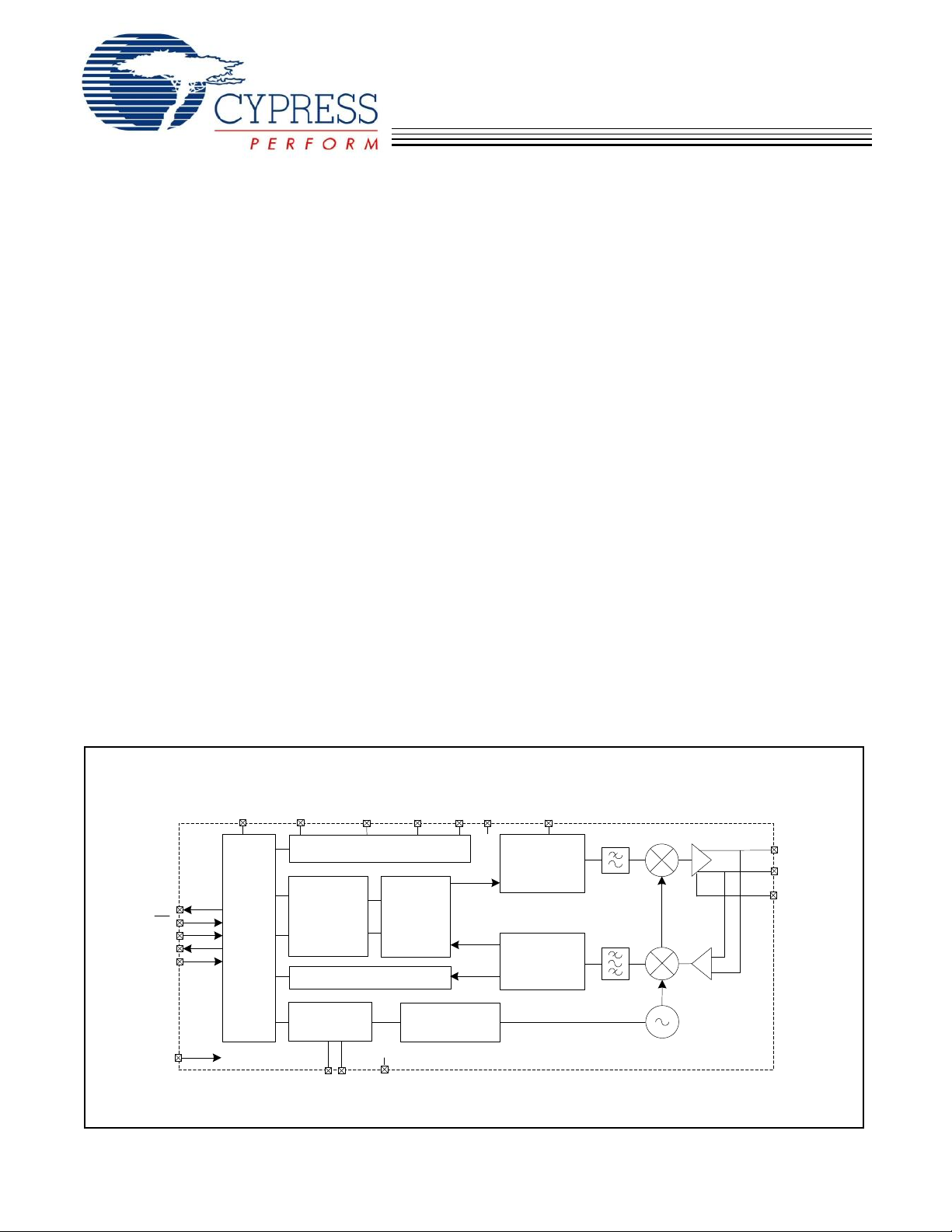
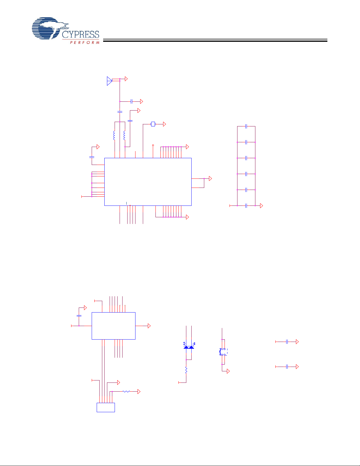
Block Diagram
RSSI
Xtal Osc
Power Management
L/D
V
REG
V
BAT
V
DD
RF
BIAS
RST
V
IO
PACTL
V
CC
GND
CYRF6936 Simplified Block Diagram
Applications
• 2.4 GHz Direct Sequence Spread S p ectrum (DSSS) radio
transceiver
• Operates in the unlicensed worldwide Industrial, Scientific
and Medical (ISM) band (2.400 GHz–2.483 GHz)
• 21 mA operating current (Transmit @ –5 dBm)
• Transmit power up to +4 dBm
• Receive sensitivity up to –97 dBm
• Sleep Current <1 μA
• Operating range: 10m+
• DSSS data rates up to 250 kbps, GFSK data rate of 1 Mbps
• Low external component count
• Auto Transaction Sequencer (ATS) - no MCU intervention
• Framing, Length, CRC16, and Auto ACK
• Power Management Unit (PMU) for MCU/Sensor
• Fast Startup and Fast Channel Changes
• Separate 16-byte Transmit and Receive FIFOs
• AutoRate™ - dynamic data rate reception
• Receive Signal Strength Indication (RSSI)
• Serial Peripheral Interface (SPI) control while in sleep mode
• 4 MHz SPI microcontroller interface
• Battery Voltage Monitoring Circuitry
• Supports coin-cell operated applications
• Operating voltage from 1.8V to 3.6V
• Operating temperature from 0 to 70°C
• Space saving 40-pin QFN 6x6 mm package
• Wireless Keyboards and Mice
• Wireless Gamepads
• Remote Controls
•Toys
• VOIP and Wireless Headsets
• White Goods
• Consumer Electronics
• Home Automation
• Automatic Meter Readers
• Personal Health and Entertainment
Applications Support
See www.cypress.com for development tools, reference
designs, and application notes.
Functional Description
The CYRF6936 WirelessUSB™ LP radio is a second gene ration member of Cypress’s WirelessUSB Radio
System-On-Chip (SoC) family. The CYRF6936 is interoperable with the first generation CYWUSB69xx devices. The
CYRF6936 IC adds a range of enhanced features, including
increased operating voltage range, reduced supply current in
all operating modes, higher data rate options, and reduced
crystal start up, synthesizer settling and link turnaround times.
Cypress Semiconductor Corporation • 198 Champion Court • San Jose, CA 95134-1709 • 408-943-2600
Document #: 38-16015 Rev. *G Revised April 2, 2007
CYRF6936
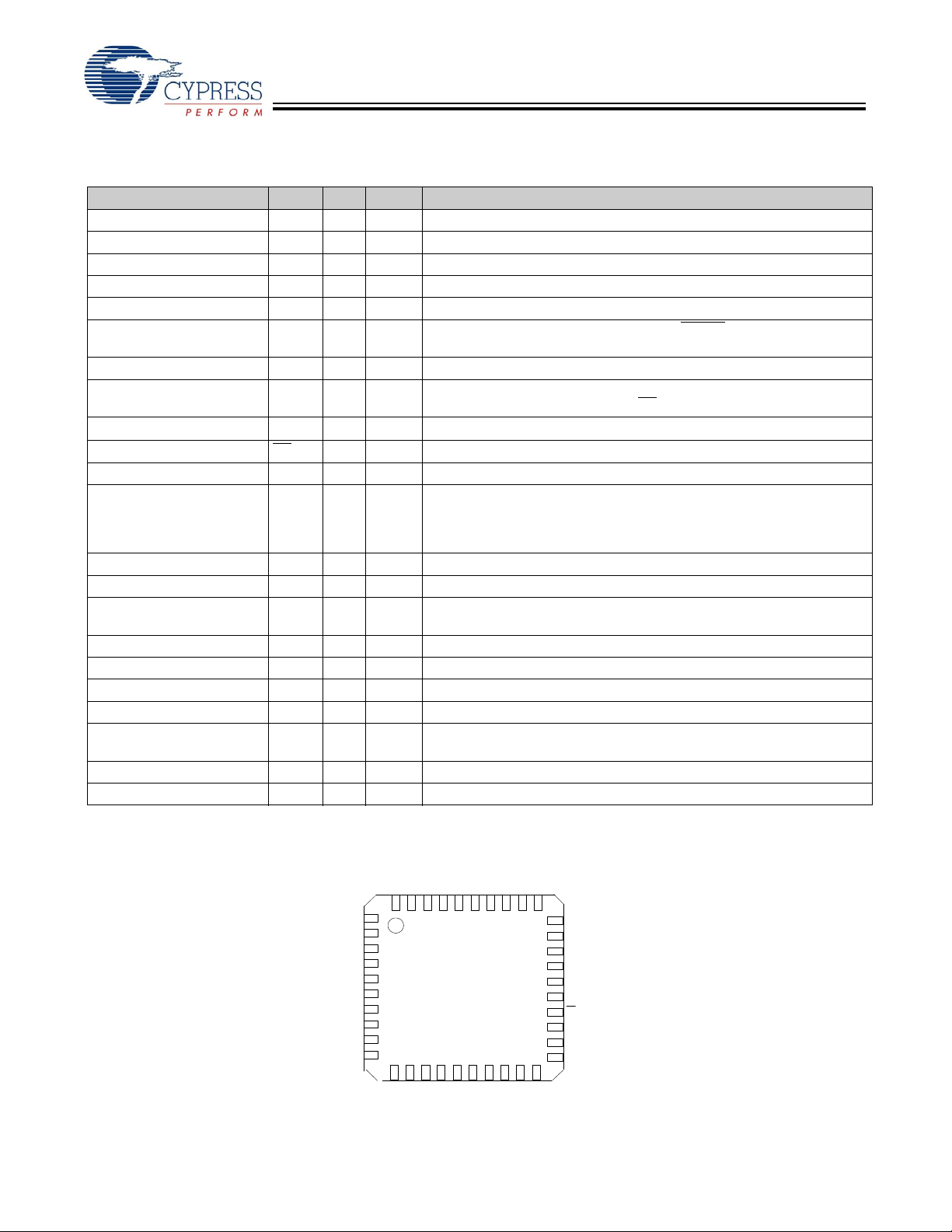
Pin Descriptions
CYRF6936
40-lead QFN
RF
BIAS
NC
NC
V
BAT
V
CC
V
BAT
XTAL
V
CC
NC
NC
V
REG
NC
NC
V
BAT
L/D
NC
NC
V
IO
V
DD
RST
RFNNCNCVCCNCNCRESV
NC
GND
RF
P
NC
SS
SCK
IRQ / GPIO
MOSI / SDAT
MISO / GPIO
XOUT / GPIO
PACTL / GPIO
NC
NC
23
24
25
26
27
28
29
30
22
21
13141516171819
20
12
11
10
9
2
8
7
6
1
3
5
4
40
3932383736
31
333534
* E-PAD BOTTOM SIDE
CYRF6936
Top View*
Pin # Name Type Default Description
13 RF
11 RF
10 RF
30 PACTL I/O O Control signal for external PA, T/R switch, or GPIO
1 XTAL I I 12 MHz crystal
29 XOUT I/O O Buffered 0.75, 1. 5 , 3, 6 or 12 MHz clock, PACTL, or GPIO.
25 SCK I I SPI clock
28 MISO I/O Z SPI data output pin (Master In Slave Out), or GPIO (in SPI 3-pin mode).
27 MOSI I/O I
24 SS I I SPI enable, active LOW assertion. Enables and frames transfers
26 IRQ I/O O Interrupt output (configurable active HIGH or LOW), or GPIO
34 RST I I Device reset. Internal 10 kohm pull down resistor. Active HIGH, typically
37 L/D O PMU inductor/diode connection, when used. If not used, connect to GND
40 V
35 V
6, 8, 38 V
3, 7, 16 V
33 V
REG
DD
BAT
CC
IO
19 RESV I Must be connected to GND
2, 4, 5, 9, 14, 15, 18, 17, 20,
NC NC Connect to GND
21, 22, 23, 32, 36, 39, 31
12 GND GND Ground
E-PAD GND GND Ground
I/O I Differential RF signal to/from antenna
N
I/O I Differential RF signal to/from antenna
P
O O RF I/O 1.8V reference voltage
BIAS
Tri-states in sleep mode (configure as GPIO drive LOW)
Tri-states when SPI 3PIN = 0 and SS
is deasserted
SPI data input pin (Master Out Slave In), or SDAT
connect through a 0.47 μF capacitor to V
the first time power is applied to the radio. Otherwise the state of the radio
Must have RST = 1 event
BAT.
control registers is unknown
Pwr PMU boosted output voltage feedback
Pwr Decoupling pin for 1.8V logic regulator, connect through a 0.47 μF
capacitor to GND
Pwr V
Pwr VCC = 2.4V to 3.6V. Typically connected to V
= 1.8V to 3.6V. Main supply
BAT
REG
Pwr I/O interface voltage, 1.8–3.6V
Figure 1. CYRF6936, 40 QFN – Top View
Document #: 38-16015 Rev. *G Page 2 of 40

CYRF6936
Functional Overview
P SOP 1 SOP 2 Length CRC 16
Payload Data
Preamble
n x 16us
1st Framing
Sym bol*
2nd Framing
Sym bol*
Packet
length
1 Byte
Period
*Note:32 or 64us
The CYRF6936 IC provides a complete WirelessUSB SPI to
antenna wireless MODEMs. The SoC is designed to
implement wireless device links operating in the worldwide
2.4 GHz ISM frequency band. It is intended for systems
compliant with worldwide regulations covered by ETSI EN 301
489-1 V1.41, ETSI EN 300 328-1 V1.3.1 (Europe), FCC CFR
47 Part 15 (USA and Industry Canada) and TELEC
ARIB_T66_March, 2003 (Japan).
The SoC contains a 2.4 GHz, 1 Mbps GFSK radio transceiver,
packet data buffering, packet framer, DSSS baseband
controller, Received Signal Strength Indication (RSSI), and
SPI interface for data transfer and device configuration.
The radio supports 98 discrete 1 MHz channels (regulations
may limit the use of some of these channels in certain jurisdictions).
The baseband performs DSSS spreading/despreading, Start
of Packet (SOP), End of Packet (EOP) detection, and CRC16
generation and checking. The baseband may also be
configured to automatically transmit Acknowledge (ACK)
handshake packets whenever a valid packet is received.
When in receive mode, with packet framing enabled, the
device is always ready to receive data transmitted at any of the
supported bit rates, enabling the implementation of mixed-rate
systems in which different devices use different data rates.
This also enables the implementation of dynamic data rate
systems that use high data rates at shorter distances or in a
low-moderate interference environment or both, and change
to lower data rates at longer distances or in high interference
environments or both.
In addition, the CYRF6936 IC has a Power Management Unit
(PMU), which allows direct connection of the device to any
battery voltage in the r ange 1.8V t o 3.6V. The PMU conditions
the battery voltage to provide the supply voltages required by
the device, and may supply external devices.
Data Transmission Modes
The SoC supports four different data transmission modes:
• In GFSK mode, data is transmitted at 1 Mbps, without any
DSSS.
• In 8DR mode, eight bits are encoded in each derived code
symbol transmitted.
• In DDR mode, two bits are encoded in each derived code
symbol transmitted. (As in the CYWUSB6934 DDR mode).
• In SDR mode, one bit is encoded in each derived code
symbol transmitted. (As in the CYWUSB6934 standard
modes.)
Both 64 chip and 32 chip Pseudo Noise (PN) codes are
supported. The four data transmission modes apply to the data
after the SOP. In particular the length, data, and CRC16 are all
sent in the same mode. In general, lower data rates reduce
packet error rate in any given environment.
Link Layer Modes
The CYRF6936 IC device supports the following data packet
framing features:
SOP – Packets begin with a two-symbol Start of Packet
marker. This is required in GFSK and 8DR modes, but is
optional in DDR mode and is not supported in SDR mode ; if
framing is disabled then an SOP event is inferred whenever
two successive correlations are detected. The
SOP_CODE_ADR code used for the SOP is different from that
used for the “body” of the packet, and if desired may be a
different length. SOP must be configured to be the same
length on both sides of the link.
Length – There are two options for detecting the end of a
packet. If SOP is enabled, then the length field should be
enabled. GFSK and 8DR must enable the length field. This is
the first eight bits after the SOP symbol, and is transmitted at
the payload data rate. When the length field is enabled, an End
of Packet condition is inferred after reception of the number of
bytes defined in the length field, plus two bytes for the CRC16
(when enabled—see the following paragraph). The alternative
to using the length field is to infer an EOP condition from a
configurable number of successive noncorrelations; this
option is not available in GFSK mode and is only recommended when using SDR mode.
CRC16 – The device may be configured to append a 16 bit
CRC16 to each packet. The CRC16 uses the USB CRC
polynomial with the added programmability of the seed. If
enabled, the receiver verifies the calculated CRC16 for the
payload data against the received value in the CRC16 field.
The seed value for the CRC16 calculation is configurable, and
the CRC16 transmitted may be calculated using either the
loaded seed value or a zero seed; the received data CRC16
is checked against both the configured and zero CRC16
seeds.
CRC16 detects the following errors:
• Any one bit in error
• Any two bits in error (no matter how far apart, which column,
and so on)
• Any odd number of bits in error (no matter where they are)
• An error burst as wide as the checksum itself
Figure 2 shows an example packet with SOP, CRC16 and
lengths fields enabled, and Figure 3 on page 4 shows a
standard ACK packet.
Figure 2. Example Packet Format
Document #: 38-16015 Rev. *G Page 3 of 40

CYRF6936
Figure 3. Example ACK Packet Format
P SOP 1 SO P 2 CRC 16
Preamble
n x 16us
1st Fram ing
Sym bol*
2nd Framing
Sym bol*
CRC field from
received packet.
2 Byte periods
*Note:32 or 64us
Packet Buffers
All data transmission and reception uses the 16 byte packet
buffers—one for transmission and one for reception.
The transmit buffer allows a complete packet of up to 16 bytes
of payload data to be loaded in one burst SPI transaction, and
then transmitted with no further MCU intervention. Similarly,
the receive buffer allows an entire packet of payload data up
to 16 bytes to be received with no firmware intervention
required until packet reception is complete.
The CYRF6936 IC supports packets up to 255 bytes.
However, actual maximum packet length depends on the
accuracy of the clock on each end of the link and the data
mode; interrupts are provided to allow an MCU to use the
transmit and receive buffers as FIFOs. When transmitting a
packet longer than 16 bytes, the MCU can load 16 bytes
initially, and add further bytes to the transmit buffer as transmission of data creates space in the buffer. Similarly, when
receiving packets longer than 16 bytes, the MCU must fetch
received data from the FIFO periodically during packet
reception to prevent it from overflowing.
Auto Transaction Sequencer (ATS)
The CYRF6936 IC provides automated support for transmission and reception of acknowledged data packets.
When transmitting in transaction mode, the device automatically:
• Starts the crystal and synthesizer
• Enters transmit mode
• Transmits the packet in the transmit buffer
• Transitions to receive mode and waits for an ACK packet
• Transitions to the transaction end state when either an ACK
packet is received, or a timeout period expires
Similarly, when receiving in transaction mode, the device
automatically:
• Waits in receive mode for a valid packet to be received
• Transitions to transmit mode, transmits an ACK packet
• Transitions to the transaction end state (receive mode to
await the next packet, and so on.)
The contents of the packet buffers are not affected by the
transmission or reception of ACK packets.
In each case, the entire packet transaction takes place without
any need for MCU firmware action (as long as packets of 16
bytes or less are used); to transmit data the MCU simply must
load the data packet to be transmitted, set the length, and set
the TX GO bit. Similarly, when receiving pa ckets in transaction
mode, firmware simply must retrieve the fully received packet
in response to an interrupt request indicating reception of a
packet.
Backward Compatibility
The CYRF6936 IC is fully interoperable with the main modes
of the first generation devices. The 62.5 kbps mode is
supported by selecting 32 chip DDR mode. Similarly, the
15.675 kbps mode is supported by selecting 64 chip SDR
mode.
In this way, a suitab ly configured CYRF6936 IC device may
transmit data to or receive data from a first generation device,
or both. Backwards compatibility requires disabling the SOP,
length, and CRC16 fields.
Data Rates
By combining the PN code lengths and data transmission
modes described previously, the CYRF6936 IC supports the
following data rates:
• 1000 kbps (GFSK)
• 250 kbps (32 chip 8DR)
• 125 kbps (64 chip 8DR)
• 62.5 kbps (32 chip DDR)
• 31.25 kbps (64 chip DDR)
• 15.625 kbps (64 chip SDR)
Functional Block Overview
2.4 GHz Radio
The radio transceiver is a dual conversion low IF architecture
optimized for power and range/robustness. The radio employs
channel-matched filters to achieve high performance in the
presence of interference. An integrated Power Amplifier (PA)
provides up to +4 dBm transmit power, with an output power
control range of 34 dB in seven steps. The supply current of
the device is reduced as the RF output power is reduced.
Table 1. Internal PA Output Power Step Table
PA Setting Typical Output Power (dBm)
7+4
60
5–5
4 –13
3 –18
2 –24
1 –30
0 –35
Document #: 38-16015 Rev. *G Page 4 of 40

CYRF6936
Table 2. Typical Range Observed Table
Environment Typical Range (meters)
Outdoor 30
Office 20
Home 15
Note: Range observed with CY4636 WirelessUSB LP KBM v1.0 (Keyboard)
Frequency Synthesizer
Before transmission or reception may begin, the frequency
synthesizer must settle. The settling time varies depending on
channel; 25 fast channels are provided with a maximum
settling time of 100 μs.
The ‘fast channels’ (less than 100 μs settling time) are every
third channel, starting at 0 up to and including 72 (for example,
0, 3, 6, 9….69, 72).
Baseband and Framer
The baseband and framer blocks provide the DSSS encoding
and decoding, SOP generation and reception and CRC16
generation and checking, as well as EOP detection and length
field.
Packet Buffers and Radio Configuration Registers
Packet data and configuration registers are accessed through
the SPI interface. All configuration registers are directly
addressed through the address field in the SPI packet (as in
the CYWUSB6934). Configuration registers allow configuration of DSSS PN codes, data rate, operating mode, interrupt
masks, interrupt status, and so on.
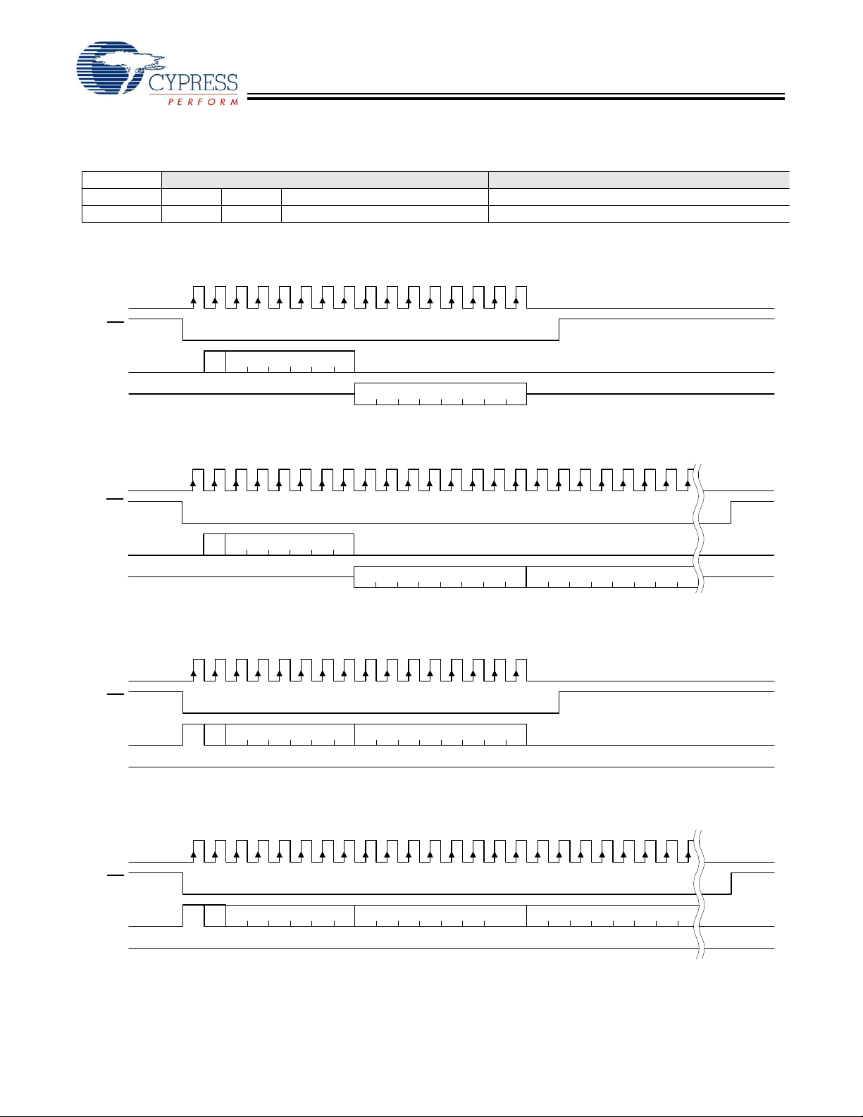
SPI Interface
The CYRF6936 IC has an SPI interface supporting communications between an application MCU and one or more slave
devices (including the CYRF6936). The SPI interface supports
single-byte and multi-byte serial transfers using either 4-pin or
3-pin interfacing. The SPI communications interface consists
of Slave Select (SS
Out-Slave In (MOSI), Master In-Slave Out (MISO), or Serial
Data (SDA T).
The SPI communications are as follows:
• Command Direction (bit 7) = ‘1’ enables SPI write transaction. A ‘0’ enables SPI read transactions.
• Command Increment (bit 6) = ‘1’ enables SPI auto address
increment. When set, the address field automatically increments at the end of each data byte in a burst access,
otherwise the same address is accessed.
), Serial Clock (SCK), and Master
• Six bits of address.
• Eight bits of data.
The device receives SCK from an application MCU on the SCK
pin. Data from the application MCU is shifted in on the MOSI
pin. Data to the application MCU is shifted out on the MISO
pin. The active LOW Slave Select (SS
to initiate an SPI transfer.
The application MCU can initiate SPI data transfers using a
multi-byte transaction. The first byte is the Command/Address
byte, and the following bytes are the data bytes as shown in
Figure 4 through Figure 7 on page 6.
The SPI communications interface has a burst mechanism,
where the first byte can be followed by as many data bytes as
desired. A burst transaction is terminated by deassertin g the
slave select (SS
The SPI communications interface single read and burst read
sequences are shown in Figure 5 and Figure 6, respectively.
The SPI communications interface single write and burst write
sequences are shown in Figure 7 and Figure 8, respectively.
This interface may optionally be operated in a 3-pin mode with
the MISO and MOSI functions combined in a single bidirectional data pin (SDA T). When using 3-pin mode, user firmware
should ensure that the MOSI pin on the MCU is in a high
impedance state except when MOSI is actively transmitting
data.
The device registers may be written to or read from one byte
at a time, or several sequential register locations may be
written/read in a single SPI transaction using incrementing
burst mode. In addition to single byte configuration registers,
the device includes register files; register files are FIFOs
written to and read from using nonincrementing burst SPI
transactions.
The IRQ pin function may optionally be multiplexed onto the
MOSI pin; when this option is enabled the IRQ function is not
available while the SS
ration, user firmware should ensure that the MOSI pin on the
MCU is in a high impedance state whenever the SS
HIGH.
The SPI interface is not dependent on the internal 12 MHz
clock. Registers may therefore be read from or written to while
the device is in sleep mode, and the 12 MHz oscillator
disabled.
The SPI interface and the IRQ and RST pins have a separate
voltage reference pin (V
directly to MCUs operating at voltages below the CYRF6936
IC supply voltage.
= 1).
pin is LOW. When using this configu-
), enabling the device to interface
IO
) pin must be asserted
pin is
Document #: 38-16015 Rev. *G Page 5 of 40
CYRF6936
Figure 4. SPI Transaction Format
Byte 1 Byte 1+N
Bit # 7 6 [5:0] [7:0]
Bit Name DIR INC Address Data
DIR
0
INCA5A4A3A2A1A0
D7 D6 D5 D4 D3 D2 D1 D0
SCK
MOSI
SS
MISO
cmd addr
data to mcu
DIR
0
INCA5A4A3A2A1A0
D7 D6 D5 D4 D3 D2 D1 D0 D7 D6 D5 D4 D3 D2 D1 D0
data to mcu
1
cmd addr
data to mcu
1+N
SCK
MOSI
SS
MISO
DIR
1
INCA5A4A3A2A1A0
D7 D6 D5 D4 D3 D2 D1 D0
SCK
MOSI
SS
MISO
cmd addr data from mcu
DIR
1
INCA5A4A3A2A1A0
D7 D6 D5 D4 D3 D2 D1 D0
SCK
MOSI
SS
MISO
cmd addr data from mcu
1
D7 D6 D5 D4 D3 D2 D1 D0
data from mcu
1+N
Figure 5. SPI Single Read Sequence
Figure 6. SPI Incrementing Burst Read Sequence
Figure 7. SPI Single Write Sequence
Figure 8. SPI Incrementing Burst Write Sequence
Document #: 38-16015 Rev. *G Page 6 of 40

CYRF6936
Interrupts
The device provides an interrupt (IRQ) output, which is configurable to indicate the occurrence of various different events.
The IRQ pin may be programmed to be either active HIGH or
active LOW, and be either a CMOS or open drain output. A full
description of all the available interrupts can be found in
“Register Descriptions” on page 12.
The CYRF6936 IC features three sets of interrupts: transmit,
receive, and system interrupts. These interrupts all share a
single pin (IRQ), but can be independently enabled/disa bled.
The contents of the enable registers are preserved when
switching between transmit and receive modes.
If more than one interrupt is enabled at any time, it is
necessary to read the relevant status register to determine
which event caused the IRQ pin to assert. Even when a given
interrupt source is disabled, the status of the condition that
would otherwise cause an interrupt can be determined by
reading the appropriate status register. It is therefore possible
to use the devices without the IRQ pin by polling the status
registers to wait for an event, rather than using the IRQ pin.
Clocks
A 12 MHz crystal (30 ppm or better) is directly connected
between XTAL and GND without the need for external capacitors. A digital clock out function is provided, with selectable
output frequencies of 0.75, 1.5, 3, 6, or 12 MHz. This output
may be used to clock an external microcontroller (MCU) or
ASIC. This output is enabled by default, but may be disabled.
Listed below are the requirements for the crystal to be directly
connected to XTAL pin and GND.
• Nominal Frequency: 12 MHz
• Operating Mode: Fundamental Mode
• Resonance Mode: Parallel Resonant
• Frequency Initial Stability: ±30 ppm
• Series Resistance: <
• Load Capacitance: 10 pF
• Drive Level: 10 µW–100 µW
Power Management
The operating voltage of the device is 1.8V to 3.6V DC, which
is applied to the V
fully static sleep mode by writing to the FRC END = 1 and END
STATE = 000 bits in the XACT_CFG_ADR register over the
SPI interface. The device enters sleep mode within 35 µs after
the last SCK positive edge at the end of this SPI transaction.
Alternatively, the device may be configured to automatically
enter sleep mode after completing packet transmission or
reception. When in sleep mode, the on-chip oscillator is
stopped, but the SPI interface remains functional. The device
wakes from sleep mode automatically when the device is
60 ohms
pin. The device can be shut down to a
BAT
commanded to enter transmit or receive mode. When
resuming from sleep mode, there is a short delay while the
oscillator restarts. The device can be configured to assert the
IRQ pin when the oscillator has stabilized.
The output voltage (V
(PMU) is configurable to several minimum values between
2.4V and 2.7V. V
(average load) to external devices. It is possible to disable the
PMU, and to provide an externally regulated DC supply
voltage to the device’s main supply in the range 2.4V to 3.6V.
The PMU also provides a regulated 1.8V supply to the logic.
The PMU is designed to provide high boost efficiency
(74–85% depending on input voltage, output voltage and load)
when using a Schottky diode and power inductor, eliminating
the need for an external boost converter in many systems
where other components require a boosted voltage. However,
reasonable efficiencies (69–82% depending on input voltage,
output voltage, and load) may be achieved when using low
cost components such as SOT23 diodes and 0805 inductors.
The PMU also provides a configurable low battery detection
function, which may be read over the SPI interface. One of
seven thresholds between 1.8V and 2.7V may be selected.
The interrupt pin may be configured to assert when the voltage
on the V
is not a latched event. Battery monitoring is disabled when the
device is in sleep mode.
Low Noise Amplifier and Received Signal Strength Indication
The gain of the receiver can be controlled directly by clearing
the AGC EN bit and writing to the Low Noise Amplifier (LNA)
bit of the RX_CFG_ADR register. Clearing the LNA bit reduces
the receiver gain approximately 20 dB, allowing accurate
reception of very strong received signals (for example when
operating a receiver very close to the transmitter). Approximately 30 dB of receiver attenuation can be a dded b y se tting
the Attenuation (ATT) bit; this allows data reception to be
limited to devices at very short ranges. Disabling AGC and
enabling LNA is recommended unless receiving from a device
using external PA.
When the device is in receive mode the RSSI_ADR registe r
returns the relative signal strength of the on-channel signal
power.
When receiving, the device automatically measures and
stores the relative strength of the signal being received as a
five bit value. An RSSI reading is taken automatically when the
SOP is detected. In addition, a new RSSI reading is taken
every time the previous reading is read from the RSSI_ADR
register, allowing the background RF energy level on any
given channel to be easily measured when RSSI is read when
no signal is being received. A new reading can occur as fast
as once every 12 µs.
BAT
REG
pin falls below the configured threshold. LV IRQ
) of the Power Management Unit
REG
may be used to provide up to 15 mA
Document #: 38-16015 Rev. *G Page 7 of 40
CYRF6936
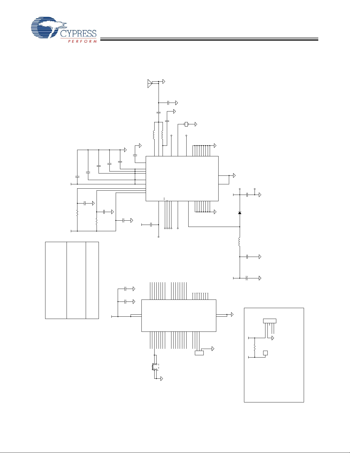
Application Examples
SDATA
ISSP
SCLK
XRES
BIND
Serial debug
header
Layout J3 and J2.1 in a
0.100" spacing
configuration
E-PAD must be soldered to ground.
Radio Decoupling Caps
RF VCO
and VCO
Buffer
Filter
The power supply decoupling shown for VBAT0
is a recommended cost effective
configuration:
C6=No Load R2= 1ohm C7=10uF ceramic.
For this configuration, it is required that
C18 be installed.
An alternate decoupling configuration is
the following:
C6=47uF ceramic R2=0ohm C7=.047uF.
For this configuration, it is not required
to load C18.
For reference design part numbers, please
refer to the Bill of Materials file
121-26504_A.xls.
A 2-pin jumper
installed from J3.1
to J2.1 enables the
radio to power the
processor. Jumper
removal is required
when programming U2
to disconnect the
radio from the
Miniprog 5V source.
R1 is a zero ohm
resistor that should
be installed for
production units
only, following
programming.
MISO
MOSI
P1_1
SCK
P1_0
MISO
nSS
IRQ
MOSI
CLKOUT
RST
SCK
COL16
COL10
COL17
COL9
COL13
P1_0
COL15
COL18
COL12
COL11
COL14
nSS
P1_1
COL5
COL3
COL2
COL8
COL1
COL6
COL7
COL4
ROW5
ROW4
ROW6
ROW2
ROW7
ROW1
ROW8
ROW3
IRQ
SW1
PACTL
EVCC
VCC
VBAT
VBAT
VCC
VBAT
VCC
EVCC
SOT23
D1
BAT400D
2 1
IND0402
L2
1.8 nH
U2
CY7C60123-PVXC
30
161718
292826
25
19
23
12
5
7
24
10
2043214222
6
34353637383940
41
131415
313233
2744
1198412346474845
P1_4 / SCLK
P0_7
P0_6 / TIO1
P0_5 / TIO0
P1_3 / SSEL
P1_2
P1_1
P1_0
P0_4 / INT2
P0_0 / CLKIN
P2_3
VDD1
P4_0
VSS1
P2_5
P0_3 / INT1
P4_3
P0_2 / INT0
P4_2
P0_1 / CLKOUT
P4_1
P3_0
P3_1
P3_2
P3_3
P3_4
P3_5
P3_6
P3_7
P2_2
P2_1
P2_0
P1_5 / SMOSI
P1_6 / SMISO
P1_7
VDD2VSS2
P2_4
P2_6
P2_7
NC4
NC1
NC2
NC3
NC6
NC7
NC8
NC5
S1
SW PUSHBUTTON
1A
2A
1B
2B
0402
C5
0.47 uFd
IND0603
L1
22 nH
0603
R1
NO LOAD
TV4
0402
C8
1 uFd 6.3V
0402
C11
0.047 uFd
0402
C17
0.47 uFd
0805
R2
1 1%
L3
10 uH
TV5
0805
C12
10 uFd 6.3V
0805
C7
10 uFd 6.3V
0402
C20
0.01 uFd
0402
C16
0.047 uFd
J3
1 PIN HDR
1
TV8
J2
5 PIN HDR
12345
J4
3 PIN HDR
123
0402
R3
47
TP2
TP1
0402
C13
0.047 uFd
U1
CYRF6936
36
4
8
1916202
252726
29
34
28
3
7
5
13
6
37
1
24
39
40
41
35
9
14
10
11
12
151718
21302233233132
38
NC15
NC2
VBAT2
RESV
VCC3
NC9NC1
SCK
MOSI
IRQ
XOUT
RST
MISO
VCC1
VCC2
NC3
RFn
VBAT1
L/D
XTAL
SS
NC16
VREG
E-PAD
VDD
NC4
NC5
RFbias
RFp
GND1
NC6
NC7
NC8
NC10
PACTL
NC11
VIO
NC12
NC13
NC14
VBAT0
0402
C3
2.0 pFd
0402
C1
15 pFd
+
E
C18
100 uFd 10v
0402
C15
0.047 uFd
TV7
TV6
ANT1
WIGGLE 63
1
2
0402
C4
1.5 pFd
Y1
12 MHz Crystal
TV2
1210
C6
No Load
0402
C10
0.047 uFd
TV1
TV3
0402
C19
0.01 uFd
0402
C9
0.047 uFd
Figure 9. Recommended Circuit for Systems Where V
May Fall Below 2.4V
BAT
Document #: 38-16015 Rev. *G Page 8 of 40

CYRF6936
Table 3. Recommended Bill of Materials for Systems Where V
May Fall Below 2.4V
BAT
Item Qty CY Part Number Reference Description Manufacturer Mfr Part Number
1 1 NA ANT1 2.5GHZ H-STUB WIGGLE ANTEN-
2 1 730-10012 C1 CAP 15PF 50V CERAMIC NPO 0402 Panasonic ECJ-0EC1H150J
3 1 730-11955 C3 CAP 2.0 PF 50V CERAMIC NPO
4 1 730-11398 C4 CAP 1.5PF 50V CERAMIC NPO
5 2 730R-13322 C5,C17 CAP CER 0.47UF 6.3V X5R 0402 Murata GRM155R60J474KE19D
6 2 730-13037 C12,C7 CAP CERAMIC 10UF 6.3V X5R 0805 Kemet C0805C106K9PACTU
7 1 730-13400 C8 CAP 1 uF 6.3V CERAMIC X5R 0402 Panasonic ECJ-0EB0J105M
8 6 730-13404 C9,C10,C11,
9 1 730-11952 C19 CAP 0.1 uF 50V CERAMIC X5R 0402 Kemet C0402C104K8PACTU
10 1 710-13201 C18 CAP 100UF 10V ELECT FC Panasonic - ECG EEU-FC1A101S
11 4 730-10794 C20,C23,C24,C25CAP 10000PF 16V CERAMIC 0402
12 3 730-13036 C26,C27,C28 CAP CERAMIC 1.0UF 10V X5R 0603 Kemet C0603C105K8PACTU
13 1 800-13248 D1 DIODE SCHOTTKY 20V 1A SMA Taiwan
14 1 420-11964 J1 HEADER 1 POS 0.230 HT MODII
15 1 420-11496 J3 CONN HDR BRKWA Y 5POS STR AU
16 1 800-13401 L1 INDUCTOR 22NH 2% FIXED 0603
17 1 800-11651 L2 INDUCTOR 1.8NH +-.3NH FIXED
18 1 800-13253 L3 COIL 10UH 1.23A UNSHIELDED
19 1 610-13402 R1 RES 47 OHM 1/16W 5% 0402 SMD Panasonic - ECG ERJ-2GEJ470X
20 1 620-10539 R2 RES 100K OHM 1/16W 5% 0603
21 3 tmp R6,R7,R8 RES CHIP 5.11 OHM 1/16W 1% 0603
22 1 630-11356 R9 RES 1.00 OHM 1/8W 1% 0805 SMD Yageo 9C08052A1R00FKHFT
23 1 CYRF6936-40LFC U1 IC, LP 2.4 GHz RADIO SoC QFN-40 Cypress Semiconductor CYRF6936 Rev A5
24 1 CY7C60323-PVXC U2 IC WIRELESS MICROCONTROL-
25 1 800-13259 Y1 CRYSTAL 12.00MHZ HC49 SMD eCERA GF-1200008
26 1 PDC-9302-*C PCB PRINTED CIRCUIT BOARD Cypress Semiconductor PDC-9302-*C
27 1 920-11206 LABEL1 Serial Number
28 1 920-30200 *C LABEL2 PCA # 121-30200 *C
C13,C15,C16
NA FOR 63MIL PCB
0402
0402 SMD
CAP 0.047 uF 50V CERAMIC X5R
0402
SMD
0.100CL
PCB
SMD
0402 SMD
SMD
SMD
SMD
LER SSOP28
NA NA
Kemet C0402C209C5GACTU
PANASONIC ECJ-0EC1H1R5C
AVX 0402YD473KAT2A
Panasonic - ECG ECJ-0EB1C103K
Semiconductor
AMP/Tyco 103185-1
AMP Division of TYCO 103185-5
Panasonic - ECG ELJ-RE22NGF2
Panasonic - ECG ELJ-RF1N8DF
Sumida CDH53100LC
Panasonic - ECG ERJ-3GEYJ104V
Yageo America 9C06031A5R11FGHFT
Cypress Semiconductor CY7C60323-PVXC
SS12
Document #: 38-16015 Rev. *G Page 9 of 40
CYRF6936
"BIND"
Power Supply
"CONNECT/ACTIVITY"
E-PAD must be soldered to ground.
DP
SW1
VBUS
DM
nSS
SCK
MISO
MOSI
IRQ
SW1
nLED1
nLED2
RST
nLED1
nLED2
IRQ
RST
MOSI
SCK
nSS
MISO
5V
5V
VCC
VCC
5V
VCC
VCC
5V
U1
CYRF6936
36
4
8
1916202
252726
29
34
28
3
7
5
13
6
37
1
24
39
40
41
35
9
14
10
11
12
151718
21302233233132
38
NC15
NC2
VBAT2
RESV
VCC3
NC9NC1
SCK
MOSI
IRQ
XOUT
RST
MISO
VCC1
VCC2
NC3
RFn
VBAT1
L/D
XTAL
SS
NC16
VREG
E-PAD
VDD
NC4
NC5
RFbias
RFp
GND1
NC6
NC7
NC8
NC10
PACTL
NC11
VIO
NC12
NC13
NC14
VBAT0
IND0402
L2
1.8 nH
0402
C9
0.047 uFd
J1
USB A SMT PLUG
12345
6
VBUS
DM
DP
GND
S1
S2
0402
C1
15 pFd
0402
R1
zero
D1
LED Green Red
1
2
3
4
GR
RD
C
C
0402
R2
620
ANT1
WIGGLE 32
1
2
0402
C12
1500 pFd
0402
C10
0.047 uFd
0402
C3
2.0 pFd
0402
C7
0.047 uFd
0805
C13
4.7 uFd
0805
C14
2.2 uFd
S1
SW RA PUSH
1A
1B
2A
2B
0402
C6
0.047 uFd
TV1 TV-20R Y1
12 MHz Crystal
0402
C11
0.047 uFd
0402
C4
1.5 pFd
0402
C8
0.047 uFd
U2
CY7C63803-SXC
7654321
16
15
8 11
1210
9
13
14
P0_0
P0_1
P0_2/INT0
P0_3/INT1
P0_4/INT2
P0_5/TIO0
P0_6/TIO1
MISO/P1_6
MOSI/P1_5
VSS VCC
VREGDM/P1_1
DP/P1_0
SSEL/P1_3
SCLK/P1_4
0402
C5
0.47 uFd
IND0603
L1
22 nH
Figure 10. Recommended Circuit for Systems Where V
is 2.4V to 3.6V (PMU disabled)
BAT
Document #: 38-16015 Rev. *G Page 10 of 40

CYRF6936
Table 4. Recommended Bill of Materials for Systems Where V
is 2.4V to 3.6V (PMU disabled)
BAT
Item Qty CY Part Number Reference Description Manufacturer Mfr Part Number
1 1 NA ANT1 2.5GHZ H-STUB WIGGLE ANTEN-
2 1 730-10012 C1 CAP 15PF 50V CERAMIC NPO 0402 Panasonic ECJ-0EC1H150J
3 1 730-11955 C3 CAP 2.0 PF 50V CERAMIC NPO
4 1 730-11398 C4 CAP 1.5PF 50V CERAMIC NPO
5 1 730-13322 C5 CAP 0.47 uF 6.3V CERAMIC X5R
6 6 730-13404 C6,C7,C8,C9,
7 1 730-11953 C12 CAP 1500PF 50V CERAMIC X7R
8 1 730-13040 C13 CAP CERAMIC 4.7UF 6.3V XR5
9 1 730-12003 C14 CAP CER 2.2UF 10V 10% X7R 0805 Murata Electronics
10 1 800-13333 D1 LED GREEN/RED BICOLOR 1210
11 1 420-13046 J1 CONN USB PLUG TYPE A PCB SMT ACON UAR72-4N5J10
12 1 800-13401 L1 INDUCTOR 22NH 2% FIXED 0603
13 1 800-11651 L2 INDUCTOR 1.8NH +-.3NH FIXED
14 1 610-10343 R1 RES ZERO OHM 1/16W 0402 SMD Panasonic - ECG ERJ-2GE0R00X
15 1 610-13472 R2 RES CHIP 620 OHM 1/16W 5% 0402
16 1 200-13471 S1 SWITCH LT 3.5MMX2.9MM 160GF
17 1 CYRF6936-40LFC U1 IC, LP 2.4 GHz RADIO SoC QFN-40 Cypress Semicondu ctor CYRF6936 Rev A5
18 1 CY7C63803-SXC U2 IC LOW-SPEED USB ENCORE II
19 1 800-13259 Y1 CRYSTAL 12.00MHZ HC49 SMD eCERA GF-1200008
20 1 PDC-9263-*B PCB PRINTED CIRCUIT BOARD Cypress Semiconductor PDC-9263-*B
21 1 LABEL1 Serial Number XXXXXX
22 1 LABEL2 PCA # 121-26305 **
C10,C11
NA FOR 32MIL PCB
0402
0402 SMD
0402
CAP 0.047 uF 16V CERAMIC X5R
0402
0402
0805
SMD
SMD
0402 SMD
SMD
SMD
CONTROLLER SOIC16
NA NA
Kemet C0402C209C5GACTU
PANASONIC ECJ-0EC1H1R5C
Murata GRM155R60J474KE19D
AVX 0402YD473KAT2A
Kemet C0402C152K5RACT U
Kemet C0805C475K9PACTU
North America
LITEON LTST-C155KGJRKT
Panasonic - ECG ELJ-RE22NGF2
Panasonic - ECG ELJ-RF1N8DF
Panasonic - ECG ERJ-2GEJ621X
Panasonic - ECG EVQ-P7J01K
Cypress Semiconductor CY7C63803-SXC
GRM21BR71A225KA01L
Document #: 38-16015 Rev. *G Page 11 of 40
CYRF6936
Register Descriptions
Notes
1. b = read/write; r = read only; w = write only; ‘-’ = not used, default value is undefined.
2. SOP_CODE_ADR default = 0x17FF9E213690C782.
3. DATA_CODE_ADR default = 0x02F9939702FA5CE3012BF1DB0132BE6F.
4. PREAMBLE_ADR default = 0x333302.
All registers are read and writable, except where noted. Registers may be written to or read from either individually or in sequential
groups.
Table 5. Register Map Summary
Address Mnemonic b7 b6 b5 b4 b3 b2 b1 b0 Default
0x00 CHANNEL_ADR Not Used Channel -1001000 -bbbbbbb
0x01 TX_LENGTH_ADR TX Length 00000000 bbbbbbbb
0x02 TX_CTRL_ADR TX GO TX CLR
0x03 TX_CFG_ADR Not Used Not Used
0x04 TX_IRQ_STATUS_ADR
0x05 RX_CTRL_ADR RX GO RSVD
0x06
0x07 RX_IRQ_STATUS_ADR
0x08 RX_STATUS_ADR RX ACK PKT ERR EOP ERR CRC0 Bad CRC RX Code RX Data Mode -------- rrrrrrrr
0x09 RX_COUNT_ADR RX Count 00000000 rrrrrrrr
0x0A RX_LENGTH_ADR RX Length 00000000 rrrrrrrr
0x0B PWR_CTRL_ADR PMU EN LVIRQ EN PMU Mode
0x0C XTAL_CTRL_ADR XOUT FN XSIRQ EN Not Used Not Used FREQ 000--100 bbb--bbb
0x0D IO_CFG_ADR IRQ OD IRQ POL MISO OD XOUT OD PACTL OD PACTL GPIO SPI 3PIN IRQ GPIO 00000000 bbbbbbbb
0x0E GPIO_CTRL_ADR XOUT OP MISO OP PACTL OP IRQ OP XOUT IP MISO IP PACTL IP IRQ IP 0000---- bbbbrrrr
0x0F XACT_CFG_ADR ACK EN Not Used FRC END END STATE ACK TO 1-000000 b-bbbbbb
0x10 FRAMING_CFG_ADR SOP EN SOP LEN LEN EN SOP TH 10100101 bbbbbbbb
0x11 DATA32_THOLD_A DR Not Used Not Used Not Used Not Used TH32 ----0100 ----bbbb
0x12 DATA64_THOLD_ADR Not Used Not Used Not Used TH64 ---01010 ---bbbbb
0x13 RSSI_ADR SOP Not Used LNA RSSI 0-100000 r-rrrrrr
0x14 EOP_CTRL_ADR HEN HINT EOP 10100100 bbbbbbbb
0x15 CRC_SEED_LSB_ADR CRC SEED LSB 00000000 bbbbbbbb
0x16 CRC_SEED_MSB_ADR CRC SEED MSB 00000000 bbbbbb bb
0x17 TX_CRC_LSB_ADR CRC LSB -------- rrrrrrrr
0x18 TX_CRC_MSB_ADR CRC MSB -------- rrrrrrrr
0x19 RX_CRC_LSB_ADR CRC LSB 11111111 rrrrrrrr
0x1A RX_CRC_MSB_ADR CRC MSB 11111111 rrrrrrrr
0x1B TX_OFFSET_LSB_ADR STRIM LSB 00000000 bbbbbbbb
0x1C TX_OFFSET_MSB_ADR Not Used Not Used Not Used Not Used STRIM MSB ----0000 ----bbbb
0x1D MODE_OVERRIDE_ADR RSVD RSVD FRC SE N FRC AWAKE Not Used Not Used RST 00000--0 wwwww--w
0x1E RX_OVERRIDE_ADR ACK RX RXTX DLY MAN RXACK
0x1F TX_OVERRIDE_ADR ACK TX FRC PRE RSVD
0x26 XTAL_CFG_ADR RSVD RSVD RSVD RSVD START DLY RSVD RSVD RSVD 00000000 wwwwwww
0x27 CLK_OVERRIDE_ADR RSVD RSVD RSVD RSVD RSVD RSVD RXF RSVD 00000000 wwwwwww
0x28 CLK_EN_ADR RSVD RSVD RSVD RSVD RSVD RSVD RXF RSVD 00000000 wwwwwww
0x29 RX_ABORT_ADR RSVD RSVD ABORT EN RSVD RSVD RSVD RSVD RSVD 000000 00 wwwwwww
0x32 AUTO_CAL_TIME_ADR AUTO_CAL_TIME 00000011 wwwwwww
0x35 AUTO_CAL_OFFSET_ADR AUTO_CAL_OFFSET 00000000 wwwwwww
0x39 ANALOG_CTRL_ADR RSVD R SVD RSVD RSVD RSVD RSVD RX INV ALL SLOW 000000 00 wwwwwww
Register Files
0x20 TX_BUFFER_ADR TX Buffer File -------- wwwwwww
0x21 RX_BUFFER_ADR RX Buffer File -------- rrrrrrrr
0x22 SOP_CODE_ADR SOP Code File Note 2 bbbbbbbb
0x23 DATA_CODE_ADR Data Code File Note 3 bbbbbbbb
0x24 PREAMBLE_ADR Preamble File Note 4 bbbbbbbb
0x25 MFG_ID_ADR MFG ID File NA rrrrrrrr
RX_CFG_ADR AGC EN LNA ATT HILO
OS
IRQ
RXOW
IRQ
LV
IRQ
SOPDET
IRQ
TXB15
IRQEN
DATA CODE
LENGTH DATA MODE PA SETTING
TXB15
IRQ
RXB16
IRQEN
RXB16
IRQ
Force
TXB8
IRQEN
TXB8
IRQ
RXB8
IRQEN
RXB8
IRQ
Not Used LVI TH PMU OUTV 10100000 bbb-bbbb
FRC
RXDR DIS CRC0 DIS RXCRC ACE Not Used
MAN
TXACK OVRD ACK DIS TXCRC RSVD TX INV
TXB0
IRQEN
TXB0
IRQ
RXB1
IRQEN
FAST TURN
EN Not Used RXOW EN VLD EN
RXB1
IRQ
TXBERR
IRQEN
TXBERR
IRQ
RXBERR
IRQEN
RXBERR
IRQ
TXC
IRQEN
TXC
IRQ
RXC
IRQEN
RXC
IRQ
TXE
IRQEN
TXE
IRQ
RXE
IRQEN
RXE
IRQ
[1]
Access
00000011 bbbbbbbb
--000101 --bbbbbb
-------- rrrrrrrr
00000111 bbbbbbbb
10010-10 bbbbb-bb
-------- brrrrrrr
0000000- bbbbbbb-
00000000 bbbbbbbb
w
w
w
w
w
w
w
w
[1]
Document #: 38-16015 Rev. *G Page 12 of 40
CYRF6936
Mnemonic CHANNEL_ADR Address 0x00
Bit 7 6 5 4 3 2 1 0
Default - 1 0 0 1 0 0 0
Read/Write - R/W R/W R/W R/W R/W R/W R/W
Function Not Used Channel
Bit 7 Not Used.
Bits 6:0 This field selects the channel. 0x00 sets 2400 MHz; 0x62 sets 2498 MHz. V alues above 0x62 are not valid. The default channel
is a fast channel above the frequency typically used in non-overlapping WiFi systems. Any write to this register impacts the time
fast (100 μs) - 0 3 6 9 12 15 18 21 24 27 30 33 36 39 42 45 48 51 54 57 60 63 66 69 72 96
medium (180 μs) - 2 4 8 10 14 16 20 22 26 28 32 34 38 40 44 46 50 52 56 58 62 64 68 70 74 76 78 80 82 84 86 88 90 92 94
slow (270 μs) - 1 5 7 11 13 17 19 23 25 29 31 35 35 37 41 43 47 49 53 55 59 61 65 67 71 73 75 77 79 81 83 85 87 89 91 93 95 97
Usable channels subject to regulation.
Do not access or modify this register during Transmit or Receive.
Mnemonic TX_LENGTH_ADR Address 0x01
Bit 7 6 5 4 3 2 1 0
Default 0 0 0 0 0 0 0 0
Read/Write R/W R/W R/W R/W R/W R/W R/W R/W
Function TX Length
Bits 7:0 This register sets the length of the packet to be transmitted. A length of zero is valid, and transmits a packet with SOP, length
Maximum packet length is limited by the delta between the transmitter and receiver crystals of 60 ppm or better.
it takes the synthesizer to settle.
and CRC16 fields (if enabled), but no data field. Packet lengths of more than 16 bytes require that some data bytes be written
after transmission of the packet has begun. Typically, length is updated prior to setting TX GO. The maximum packet length for
all packets is 40 bytes except for framed 64 chip DDR where the maximum packet length is 16 bytes.
Mnemonic TX_CTRL_ADR Address
Bit 7 6 5 4 3 2 1 0
Default 0 0 0 0 0 0 1 1
Read/Write R/W R/W R/W R/W R/W R/W R/W R/W
Function
Bit 7 Start Transmission. Setting this bit triggers the transmission of a packet. Writing ‘0’ to this flag has no effect. This bit is cleared
Bit 6 Clear TX Buffer. W riting ‘1’ to this register clears the transmit buf fer. Writing ‘0’ to this bit has no effect. The previous packet (16
Bit 5 Buffer Not Full Interrupt Enable. See TX_IRQ_STATUS_ADR for description.
Bit 4 Buffer Half Empty Interrupt Enable. See TX_IRQ_STATUS_ADR for description.
Bit 3 Buffer Empty Interrupt Enable. See TX_IRQ_STATUS_ADR for description.
Bit 2 Buffer Error Interrupt Enable. See TX_IRQ_STATUS_ADR for description.
Bit 1 Transmission Complete Interrupt Enable. TXC IRQEN and TXE IRQEN must be set together. See TX_IRQ_STATUS_ADR for
Bit 0 Transmit Error Interrupt Enable. TXC IRQEN and TXE IRQEN must be set together. See TX_IRQ_STATUS_ADR for
TX GO TX CLR
automatically at the end of packet transmission. The transmit buffer may be loaded either before or after setting this bit. If data
is loaded after setting this bit, the length of time available to load the buffer depends on the starting state (sleep, idle or synth),
the length of the SOP code, the length of preamble, and the packet data rate. For example, if starting from idle mode on a fast
channel in 8DR mode with 32 chip SOP codes the time available is 100 μs (synth start) + 32 μs (preamble) + 64 μs (SOP
length) + 32 μs (length byte) = 228 μs. If there are no bytes in the TX buffer at the end of transmission of the length field, a
TXBERR IRQ occurs.
or fewer bytes) may be retransmitted by setting TX GO and not setting this bit.
description.
description.
TXB15
IRQEN
TXB8
IRQEN
TXB0
IRQEN
TXBERR
IRQEN
TXC
IRQEN
TXE
IRQEN
0x02
Document #: 38-16015 Rev. *G Page 13 of 40
CYRF6936
Mnemonic TX_CFG_ADR Address
Bit 7 6 5 4 3 2 1 0
Default - - 0 0 0 1 0 1
Read/Write - - R/W R/W R/W R/W R/W R/W
Function
Bit 5 Data Code Length. This bit selects the length of the DATA_CODE_ADR code for the data portion of the packet. This bit is
Bits 4:3 Data Mode. This field sets the data transmission mode. 00 = 1-Mbps GFSK. 01 = 8DR Mode. 10 = DDR Mode. 11 = SDR Mode.
Bits 2:0 PA Setting. This field sets the transmit signal strength. 0 = –35 dBm, 1 = –30 dBm, 2 = –24 dBm, 3 = –18 dBm, 4 = –13 dBm,
Mnemonic TX_IRQ_STATUS_ADR Address 0x04
Bit 7 6 5 4 3 2 1 0
Default - - - - - - - Read/Write R R R R R R R R
Function OS IRQ LV IRQ TXB15 IRQ TXB8 IRQ TXB0 IRQ TXBERR IRQ TXC IRQ TXE IRQ
The state of all IRQ status bits is valid regardless of whether or not the IRQ is enabled. The IRQ output of the device is in its active state
whenever one or more bits in this register is set and the corresponding IRQ enable bit is also set. Status bits are non-atomic (different flags
may change value at different times in response to a single event).
Bit 7 Oscillator Stable IRQ Status. This bit is set when the internal crystal oscillator has settled (synthesizer sequence starts).
Bit 6 Low Voltage Interrupt Status. This bit is set when the voltage on V
Bit 5 Buffer Not Full Interrupt Status. This bit is set whenever there are 15 or fewer bytes remaining in the transmit buffer.
Bit 4 Buffer Half Empty Interrupt Status. This bit is set whenever there are eight or fewer bytes remaining in the transmit buffer.
Bit 3 Buffer Empty Interrupt Status. This bit is set at any time that the transmit buffer is empty.
Bit 2 Buffer Error Interrupt Status. This IRQ is triggered by either of two events: (1) When the transmit buffer (TX_BUFFER_ADR) is
Bit 1 Transmission Complete Interrupt Status. This IRQ is triggered when transmission is complete. If transaction mode is not
Bit 0 Transmit Error Interrupt Status. This IRQ is triggered when there is an error in transmission. This interrupt is only applicable to
Not Used Not Used
ignored when the data mode is set to GFSK. 1 = 64 chip codes. 0 = 32 chip codes.
It is recommended that firmware set the ALL SLOW bit in register ANALOG_CTRL_ADR when using GFSK data rate mode.
5 = –5 dBm, 6 = 0 dBm, 7 = +4 dBm.
interrupt is automatically disabled whenever the PMU is disabled. When enabled, this bit reflects the voltage on V
empty and the number of bytes remaining to be transmitted is greater than zero. (2) When a byte is written to the transmit buffer
and the buffer is already full. This IRQ is cleared by setting bit TX CLR in TX_CTRL_ADR.
enabled then this interrupt is triggered immediately after transmission of the last bit of the CRC16. If transaction mode is
enabled, this interrupt is triggered at the end of a transaction. Reading this register clears this bit. TXC IRQ and TXE IRQ flags
may change value at different times in response to a single event. If transaction mode is enabled and the first read of this register returns TXC IRQ = 1 and TXE IRQ = 0 then firmware must execute a second read to this register to determine if an error
occurred by examining the status of TXE. There can be a case when this bit is not triggered when ACK EN = 1 and there is an
error in transmission. If the first read of this register returns TXC IRQ = 1 and TXE IRQ = 1, then the firmware must not execute
a second read from this register for a given transaction. If an ACK is received RXC IRQ and RXE IRQ may be asserted instead
of TXC IRQ and TXE IRQ.
transaction mode. It is triggered whenever no valid ACK packet is received within the ACK timeout period. Reading this register
clears this bit. See TXC IRQ, above.
Data Code
Length
Data Mode PA Setting
is below the LVI threshold (see PWR_CTL_ADR). This
BAT
BAT
0x03
.
Document #: 38-16015 Rev. *G Page 14 of 40

CYRF6936
Mnemonic RX_CTRL_ADR
Bit 7 6 5 4 3 2 1 0
Default 0 0 0 0 0 1 1 1
Read/Write R/W R/W R/W R/W R/W R/W R/W R/W
Function
Bit 7 Start Receive. Setting this bit causes the device to transition to receive mode. If necessary, the crystal oscillator and synthesizer
Bit 6 Reserved. Must be zero.
Bit 5 Buffer Full Interrupt Enable. See RX_IRQ_STATUS_ADR for description.
Bit 4 Buffer Half Empty Interrupt Enable. See RX_IRQ_STATUS_ADR for description.
Bit 3 Buffer Not Empty Interrupt Enable. RXB1 IRQEN must not be set when RXB8 IRQEN is set and vice versa. See
Bit 2 Buffer Error Interrupt Enable. See RX_IRQ_STATUS_ADR for description.
Bit 1 Packet Reception Complete Interrupt Enable. See RX_IRQ_STATUS_ADR for description.
Bit 0 Receive Error Interrupt Enable. See RX_IRQ_STATUS_ADR for description.
RX GO RSVD
start automatically after this bit is set. Firmware must never clear this bit. This bit must not be set again until after it clears. The
recommended method to exit receive mode when an error has occurred is to force END STATE and then dummy read all
RX_COUNT_ADR bytes from RX_BUFFER_ADR or poll RSSI_ADR.SOP (bit 7) until set. See XACT_CFG_ADR and
RX_ABORT_ADR for description.
RX_IRQ_STATUS_ADR for description.
RXB16
IRQEN
RXB8
IRQEN
RXB1
IRQEN
RXBERR
IRQEN
Address 0x05
RXC
IRQEN
RXE
IRQEN
Document #: 38-16015 Rev. *G Page 15 of 40

CYRF6936
Mnemonic RX_CFG_ADR
Bit 7 6 5 4 3 2 1 0
Default 1 0 0 1 0 - 1 0
Read/Write R/W R/W R/W R/W R/W - R/W R/W
Function AGC EN LNA ATT HILO FAST TURN ENNot Used RXOW EN VLD EN
Status bits are non-atomic (different flags may change value at different times in response to a single event).
Bit 7 Automatic Gain Control (AGC) Enable. When this bit is set, AGC is enabled, and the LNA is controlled by the AGC circuit.
When this bit is cleared the LNA is controlled manually using the LNA bit. Typical applications clear this bit during initialization.
It is recommended that this bit be cleared and bit 6 (LNA) be set unless the device is used in a system where it may receive
data from a device using an external PA to transmit signals at more than +4 dBm.
Bit 6 Low Noise Amplifier (LNA) Manual Control. When AGC EN (Bit 7) is cleared, this bit controls the state of the receiver LNA;
when AGC EN is set, this bit has no effect. Setting this bit enables the LNA; clearing this bit disables the LNA. Device current in
receive mode is slightly lower when the LNA is disabled. Typical applications set this bit during initialization.
Bit 5 Receive Attenuator Enable. Setting this bit enables the receiver attenuator. The receiver attenuator may be used to desensitize
the receiver so that only very strong signals may be received. This bit should only be set when the AGC EN is disabled and the
LNA is manually disabled.
Bit 4 HILO. When FAST TURN EN is set, this bit is used to select whether the device uses the high frequency for the channel
selected, or the low frequency. 1 = hi; 0 = lo. When FAST TURN EN is not enabled this also controls the high-low bit to the
receiver and should be left at the default value of ‘1’ for high side receive injection. Typical applications clear this bit during initialization.
Bit 3 Fast Turn Mode Enable. When this bit is set, the HILO bit determines whether the device receives data transmitted 1 MHz
above the RX Synthesizer frequency or 1 MHz below the receiver synthesizer frequency. Use of this mode allows for very fast
turnaround, because the same synthesizer frequency may be used for both transmit and receive, thus eliminating the synthesizer resettling period between transmit and receive. Note that when this bit is set, and the HILO bit is cleared, received data
bits are automatically inverted to compensate for the inversion of data received on the ‘image’ frequency. Typical applications
set this bit during initialization.
Bit 1 Overwrite Enable. When this bit is set, if an SOP is detected while the receive buffer is not empty, then the existing contents of
receive buffer are lost, and the new packet is loaded into the receive buffer. When this bit is set, the RXOW IRQ is enabled. If
this bit is cleared, then the receive buffer may not be overwritten by a new packet, and whenever the receive buffer is not empty
SOP conditions are ignored, and it is not possible to receive data until the previously received packet has been completely read
from the receive buffer.
Bit 0 Valid Flag Enable. When this bit is set, the receive buffer can store up to eight bytes of data. Typically, this bit is set only when
interoperability with first generation devices is desired. See RX_BUFFER_ADR for more detail.
Address 0x06
Document #: 38-16015 Rev. *G Page 16 of 40

CYRF6936
Mnemonic RX_IRQ_STATUS_ADR
Bit 7 6 5 4 3 2 1 0
Default - - - - - - - Read/Write R/W R R R R R R R
Function RXOW IRQ SOPDET IRQ RXB16 IRQ RXB8 IRQ RXB1 IRQ RXBERR IRQ RXC IRQ RXE IRQ
The state of all IRQ Status bits is valid regardless of whether or not the IRQ is enabled. The IRQ output of the device is in its active state
whenever one or more bits in this register is set and the corresponding IRQ enable bit is also set. Status bits are non-atomic (different flags
may change value at different times in response to a single event).
Bit 7 Receive Overwrite Interrupt Status. This IRQ is triggered when the receive buffer is overwritten by a packet being received
before the previous packet has been read from the buffer. This bit is cleared by writing any value to this register. This condition
is only possible when the RXOW EN bit in RX_CFG_ADR is set. This bit must be written ‘1’ by firmware before the new packet
may be read from the receive buffer.
Bit 6 Start of packet detect. This bit is set whenever the start of packet symbol is detected.
Bit 5 Receive Buffer Full Interrupt Status. This bit is set whenever the receive buffer is full, and cleared otherwise.
Bit 4 Receive Buffer Half Full Interrupt Status. This bit is set whenever there are eight or more bytes remaining in the receive buffer.
Firmware must read exactly eight bytes when reading RXB8 IRQ.
Bit 3 Receive Buffer Not Empty Interrupt Status. This bit is set any time that there are one or more bytes in the receive buffer, and
cleared when the receive buffer is empty. It is possible, in rare cases, that the last byte of a packet may remain in the buffer
even though the RXB1 IRQ flag has cleared. This can ONLY happen on the last byte of a packet and only if the packet data is
being read out of the buffer while the packet is still being received. The flag is trustworthy under all other conditions, and for all
bytes prior to the last. When using RXB1 IRQ and unloading the packet data during reception, the user must make sure the
RX_COUNT_ADR value, after the RXC IRQ/RXE IRQ, is set and unload the last remaining bytes if the number of bytes
unloaded is less than the reported count, even though the RXB1 IRQ is not set.
Bit 2 Receive Buffer Error Interrupt Status. This IRQ is triggered in one of two ways: (1) When the receive buffer is empty and there
is an attempt to read data (2) When the receive buffer is full and more data is received; this flag is cleared when RX GO is set
and a SOP is received.
Bit 1 Packet Receive Complete Interrupt Status. This IRQ is triggered when a packet has been received. If transaction mode is
enabled, then this bit is not set until after transmission of the ACK. If transaction mode is not enabled then this bit is set as soon
as a valid packet is received. This bit is cleared when this register is read. RXC IRQ and RXE IRQ flags may change value at
different times in response to a single event. There are cases when this bit is not triggered when ACK EN = 1 and there is an
error in reception. Therefore, firmware should examine RXC IRQ, RXE IRQ, and CRC 0 to determine receive status. If the first
read of this register returns RXC IRQ = 1 and RXE IRQ = 0 then firmware must execute a second read to this register to deter-
mine if an error occurred by examining the status of RXE IRQ. If the first read of this register returns RXC IRQ = 1 and
RXE IRQ = 1, then the firmware must not execute a second read to this register for a given transaction.
Bit 0 Receive Error Interrupt Status. This IRQ is triggered when there is an error in reception. It is triggered whenever a packet is
received with a bad CRC16, an unexpected EOP is detected, a packet type (data or ACK) mismatch, or a packet is dropped
because the receive buffer is still not empty when the next packet starts. The exact cause of the error may be determined by
reading RX_STATUS_ADR. This bit is cleared when this register is read.
Address 0x07
Document #: 38-16015 Rev. *G Page 17 of 40

CYRF6936
Mnemonic RX_STATUS_ADR
Bit 7 6 5 4 3 2 1 0
Default - - - - - - - Read/Write R R R R R R R R
Function RX ACK PKT ERR EOP ERR CRC0 Bad CRC RX Code RX Data Mode
It is expected that firmware does not read this register until after RX GO self clears. Status bits are non-atomic (different flags may change
value at different times in response to a single event).
Bit 7 RX Packet Type. This bit is set when the received packet is an ACK packet, and cleared when the received packet is a standard
packet.
Bit 6 Receive Packet Type Error. This bit is set when the packet type received is not what was expected and cleared when the
packet type received was as expected. For example, if a data packet is expected and an ACK is received, this bit is set.
Bit 5 Unexpected EOP. This bit is set when an EOP is detected before the expected data length and CRC16 fields have been
received. This bit is cleared when an SOP pattern for the next packet has been received. This includes the case where there
are invalid bits detected in the length field and the length field is forced to ‘0’.
Bit 4 Zero-seed CRC16. This bit is set whenever the CRC16 of the last received packet has a zero seed.
Bit 3 Bad CRC16. This bit is set when the CRC16 of the last received packet is incorrect.
Bit 2 Receive Code Length. This bit indicates the DATA_CODE_ADR code length used in the last correctly received packet.
1 = 64 chip code, 0 = 32 chip code.
Bits 1:0 Receive Data Mode. These bits indicate the data mode of the last correctly received packet. 00 = 1 Mbps GFSK;
01 = 8DR; 10 = DDR; 11 = Not Valid. These bits do not apply to unframed packets.
Mnemonic RX_COUNT_ADR Address 0x 09
Bit 7 6 5 4 3 2 1 0
Default 0 0 0 0 0 0 0 0
Read/Write R R R R R R R R
Function RX Count
Count bits are non-atomic (updated at different times).
Address 0x08
Bits 7:0 This register contains the total number of payload bytes received during reception of the current packet. After packet reception
is complete, this register matches the value in RX_LENGTH_ADR unless there was a packet error. This register is cleared
when RX_LENGTH_ADR is automatically loaded, if length is enabled, after the SOP. Count should not be read when
RX_GO = 1 during a transaction.
Mnemonic RX_LENGTH_ADR Address 0x0A
Bit 7 6 5 4 3 2 1 0
Default 0 0 0 0 0 0 0 0
Read/Write R R R R R R R R
Function RX Length
Length bits are non-atomic (different flags may change value at different times in response to a single event).
Bits 7:0 This register contains the length field which is updated with the reception of a new length field (shortly after start of packet
detected). If there is an error in the received length field, 0x00 is loaded instead, except when using GFSK data rate, and an
error is flagged.
Document #: 38-16015 Rev. *G Page 18 of 40

CYRF6936
Mnemonic PWR_CTRL_ADR
Bit 7 6 5 4 3 2 1 0
Default 1 0 1 - 0 0 0 0
Read/Write R/W R/W R/W - R/W R/W R/W R/W
Function PMU EN LVIRQ EN PMU Mode
Bit 7 Power Management Unit (PMU) Enable. Setting this bit enables the PMU only if PMU Mode Force (bit 5) is set. Otherwise it
has no effect. See PMU Mode Force (bit 5) description for more information.
Bit 6 Low Voltage Interrupt Enable. Setting this bit enables the LV IRQ interrupt. When this interrupt is enabled, if the V
falls below the threshold set by LVI TH, a low voltage interrupt is generated. The LVI is not available when the device is in sleep
mode. The LVI event on IRQ pin is automatically disabled whenever the PMU is disabled.
Bit 5 PMU Mode Force. If this bit is set, the PMU operation is based on the state of the PMU Enable Bit (bit 7). if this bit is not set
Bits 3:2 Low Voltage Interrupt Threshold. This field sets the voltage on V
Bits 1:0 PMU Output Voltage. This field sets the minimum output voltage of the PMU. 11 = 2.4V; 10 = 2.5V; 01 = 2.6V; 00 = 2.7V . When
then the PMU is disabled in Sleep mode and enabled when not in Sleep mode, if Bit 7 = 1. If Bit 7 = 1 and Bit 5 = 1, PMU is
enabled always (even during sleep). If Bit 7 = 0 and Bit 5 = 1, PMU is disabled always. If Bit 7 = 1and Bit 5 = 0, PMU is disabled
only in Sleep Mode.
01 = 2.2V; 00 = PMU OUTV voltage.
the PMU is active, the voltage output by the PMU on V
V
pin is less than the specified maximum value, and the voltage in V
REG
Force
PFET Disable LVI TH PMU OUTV
at which the LVI is triggered. 11 = 1.8V; 10 = 2.0V;
BAT
is never less than this voltage, provided that the total load on the
REG
is greater than the specified minimum value.
BAT
Address 0x0B
voltage
BAT
The order of writing these bits impacts the value of the Sleep current I
Mnemonic XTAL_CTRL_ADR
Bit 7 6 5 4 3 2 1 0
Default 0 0 0 - - 1 0 0
Read/Write R/W R/W R/W - - R/W R/W R/W
Function XOUT FN XSIRQ EN Not Used Not Used FREQ
Bits 7:6 XOUT Pin Function. This field selects between the different functions of the XOUT pin. 00 = Clock frequency set by XOUT
FREQ; 01 = Active LOW PA Control; 10 = Radio data serial bit stream. If this option is selected and SPI is configured for 3-wire
mode then the MISO pin outputs a serial clock associated with this data stream; 11 = GPIO. To disable this output, set to GPIO
mode, and set the GPIO state in IO_CFG_ADR.
Bit 5 Crystal Stable Interrupt Enable. This bit enables the OS IRQ interrupt. When enabled, this interrupt generates an IRQ event
when the crystal has stabilized after the device has awaken from sleep mode. This event is cleared by writing ‘0’ to this bit.
Bits 2:0 XOUT Frequency. This field sets the frequency output on the XOUT pin when XOUT FN is set to 00. 0 = 12 MHz; 1 = 6 MHz,
2 = 3 MHz, 3 = 1.5 MHz, 4 = 0.75 MHz; other values are not defined.
SB
.
Address 0x0C
Document #: 38-16015 Rev. *G Page 19 of 40

CYRF6936
Mnemonic IO_CFG_ADR
Bit 7 6 5 4 3 2 1 0
Default 0 0 0 0 0 0 0 0
Read/Write R/W R/W R/W R/W R/W R/W R/W R/W
Function IRQ OD IRQ POL MISO OD XOUT OD PACTL OD PACTL GPIO SPI 3PIN IRQ GPIO
To use a GPIO pin as an input, the output mode must be set to open drain, and ‘1’ written to the corresponding output register bit.
Bit 7 IRQ Pin Drive Strength. Setting this bit configures the IRQ pin as an open drain output. Clearing this bit configures the IRQ pin
as a standard CMOS output, with the output ‘1’ drive voltage being equal to the V
Bit 6 IRQ Polarity. Setting this bit configures the IRQ signal polarity to be active HIGH. Clearing this bit configures the IRQ signal
polarity to be active low.
Bit 5 MISO Pin Drive Strength. Setting this bit configures the MISO pin as an open drain output. Clearing this bit configures the
MISO pin as a standard CMOS output, with the output ‘1’ drive voltage being equal to the V
Bit 4 XOUT Pin Drive Strength. Setting this bit configures the XOUT pin as an open drain output. Clearing this bit configures the
XOUT pin as a standard CMOS output, with the output ‘1’ drive voltage being equal to the V
Bit 3 PACTL Pin Drive Strength. Setting this bit configures the PACTL pin as an open drain output. Clearing this bit configures the
PACTL pin as a standard CMOS output, with the output ‘1’ drive voltage being equal to the V
Bit 2 PACTL Pin Function. When this bit is set, the PACTL pin is available for use as a GPIO.
Bit 1 SPI Mode. When this bit is cleared, the SPI interface acts as a standard 4-wire SPI Slave interface. When this bit is set, the SPI
interface operates in “3-Wire Mode” combining MISO and MOSI on the same pin (SDAT). The MISO pin is available as a GPIO
pin.
Bit 0 IRQ Pin Function. When this bit is cleared, the IRQ pin is asserted when an IRQ is active; the polarity of this IRQ signal is con-
figurable in IRQ POL. When this bit is set, the IRQ pin is available for use as a GPIO pin, and the IRQ function is multiplexed
onto the MOSI pin. In this case the IRQ signal state is presented on the MOSI pin whenever the SS
pin voltage.
IO
pin voltage.
IO
IO
IO
Address 0x0D
pin voltage.
pin voltage.
signal is inactive (HIGH).
Mnemonic GPIO_CTRL_ADR Address 0x0E
Bit 7 6 5 4 3 2 1 0
Default 0 0 0 0 - - - Read/Write R/W R/W R/W R/W R R R R
Function XOUT OP MISO OP PACTL OP IRQ OP XOUT IP MISO IP PACTL IP IRQ IP
To use a GPIO pin as an input, the output mode must be set to open drain, and a ‘1’ written to the corresponding output register bit.
Bit 7 XOUT Output. When the XOUT pin is configured to be a GPIO, the state of this bit sets the output state of the XOUT pin.
Bit 6 MISO Output. When the MISO pin is configured to be a GPIO, the state of this bit sets the output state of the MISO pin.
Bit 5 PACTL Output. When the PACTL pin is configured to be a GPIO, the state of this bit sets the output state of the PACTL pin.
Bit 4 IRQ Output. When the IRQ pin is configured to be a GPIO, the state of this bit sets the output state of the IRQ pin.
Bit 3 XOUT Input. The state of this bit reflects the voltage on the XOUT pin.
Bit 2 MISO Input. The state of this bit reflects the voltage on the MISO pin.
Bit 1 PACTL Input. The state of this bit reflects the voltage on the PACTL pin.
Bit 0 IRQ Input. The state of this bit reflects the voltage on the IRQ pin.
Document #: 38-16015 Rev. *G Page 20 of 40

CYRF6936
Mnemonic XACT_CFG_ADR Address 0x0F
Bit 7 6 5 4 3 2 1 0
Default 1 - 0 0 0 0 0 0
Read/Write R/W - R/W R/W R/W R/W R/W R/W
Function ACK EN Not Used FRC END END STATE ACK TO
Bit 7 Acknowledge Enable. When this bit is set, an ACK packet is automatically transmitted whenever a valid packet is received; in
this case the device is considered to be in transaction mode. After transmission of the ACK packet, the device automatically
transitions to the END STATE. When this bit is cleared, the device transitions directly to the END STATE immediately after the
end of packet transmission. This bit affects both transmitting and receiving devices.
Bit 5 Force End State. Setting this bit forces a transition to the state set in END STATE. By setting the desired END STATE at the
Bits 4:2 Transaction End State. This field defines the mode to which the device transitions after receiving or transmitting a packet. 000
Bits 1:0 ACK Timeout. When the device is configured for transaction mode, this field sets the timeout period after transmission of a
same time as setting this bit the device may be forced to immediately transition from its current state to any other state. This bit
is automatically cleared upon completion. Firmware MUST never try to force END STATE while TX GO is set, nor when RX GO
is set and a SOP has already been received (packet reception already in progress).
= Sleep Mode; 001 = Idle Mode; 010 = Synth Mode (TX); 011 = Synth Mode (RX); 100 = RX Mode. In normal use, this field is
typically set to ‘000’ or ‘001’ when the device is transmitting packets, and ‘100’ when the device is receiving packets. Note that
when the device transitions to receive mode as an END STATE, the receiver must still be armed by setting RX GO be fore the
device can begin receiving data. If the system only supports packets less than or equal to 16 bytes then firmware should examine RXC IRQ and RXE IRQ to determine the status of the packet. If the system supports packets more than 16 bytes, make
sure that END STATE is not sleep, force RXF = 1, perform receive operation, force RXF = 0, and if necessary set END STATE
back to sleep.
packet during which an ACK must be correctly received in order to prevent a transmit error condition from being detected. This
timeout period is expressed in terms of a number of SOP_CODE_ADR code lengths; if SOP LEN is set, then the timeout period
is this value multiplied by 64 μs and if SOP LEN is cleared then the timeout is this value multiplied by 32 μs. 00 = 4x; 01 = 8x,
10 = 12x; 11 = 15x the SOP_CODE_ADR code length. ACK_TO must be set to greater than 30 + Data Code Length (only for
8DR) + Preamble Length + SOP Code Length (x2).
Mnemonic FRAMING_CFG_ADR Address 0x10
Bit 7 6 5 4 3 2 1 0
Default 1 0 1 0 0 1 0 1
Read/Write R/W R/W R/W R/W R/W R/W R/W R/W
Function SOP EN SOP LEN LEN EN SOP TH
Bit 7 SOP Enable. When this bit is set, each transmitted packet begins with a SOP field, and only packets beginning with a valid
SOP field are received. If this bit is cleared, no SOP field is generated when a packet is transmitted, and packet reception
begins whenever two successive correlations against the DATA_CODE_ADR code are detected.
Bit 6 SOP PN Code Length. When this bit is set the SOP_CODE_ADR code length is 64 chips. When this bit is cleared the
SOP_CODE_ADR code length is 32 chips.
Bit 5 Packet Length Enable. When this bit is set the 8 bit value contained in TX_LENGTH_ADR is transmitted immediately after the
Bits 4:0 SOP Correlator Threshold. This is the receive data correlator threshold used when attempting to detect a SOP symbol. There
SOP field. In receive mode, the 8 bits immediately following the SOP field are interpreted as the length of the packet. When this
bit is cleared no packet length field is transmitted. 8DR always sends the packet length field (LEN EN setting is ignored). GFSK
requires user set LEN EN = 1.
is a single threshold for the SOP_CODE_ADR code. This threshold is applied independently to each of SOP1 and SOP2 fields.
When SOP LEN is set, all 5 bits of this field are used. When SOP LEN is cleared, the most significant bit is disregarded. Typical
applications configure SOP TH = 04h for SOP32 and SOP TH = 0Eh for SOP64.
Document #: 38-16015 Rev. *G Page 21 of 40

CYRF6936
Mnemonic DATA32_THOLD_ADR Address 0x11
Bit 7 6 5 4 3 2 1 0
Default - - - - 0 1 0 0
Read/Write - - - - R/W R/W R/W R/W
Function Not Used Not Used Not Used Not Used TH32
Bits 7:4 Not Used.
Bits 3:0 32 Chip Data PN Code Correlator Threshold. This register sets the correlator threshold used in DSSS modes when DATA
Mnemonic DATA64_THOLD_ADR Address 0x12
Bit 7 6 5 4 3 2 1 0
Default - - - 0 1 0 1 0
Read/Write - - - R/W R/W R/W R/W R/W
Function Not Used Not Used Not Used TH64
Bits 7:5 Not Used.
Bits 4:0 64 Chip Data PN Code Correlator Threshold. This register sets the correlator threshold used in DSSS modes when the DATA
Mnemonic RSSI_ADR Address 0x13
Bit 7 6 5 4 3 2 1 0
Default 0 - 1 0 0 0 0 0
Read/Write R - R R R R R R
Function SOP Not Used LNA RSSI
A Received Signal Strength Indicator (RSSI) reading is taken automatically when an SOP symbol is detected. In addition, an RSSI reading is
taken whenever RSSI_ADR is read. The contents of this register are not valid after the device is configured for receive mode until either a SOP
symbol is detected, or the register is (re)read. The conversion can occur as often as once every 12 μs. The approximate slope of the curve is
1.9 dB/count, but is not guaranteed.
If it is desired to measure the background RF signal strength on a channel before a packet has been received then the MCU should perform
a “dummy” read of this register, the results of which should be discarded. This “dummy” read causes an RSSI measurement to be taken, and
therefore subsequent readings of the register yield valid data.
Bit 7 SOP RSSI Reading. When set, this bit indicates that the reading in the RSSI field was taken when a SOP symbol was
Bit 5 LNA State. This bit indicates the LNA state when the RSSI reading was taken. When cleared, this bit indicates that the LNA
Bits 4:0 RSSI Reading. This field indicates the instantaneous strength of the RF signal being received at the time that the RSSI reading
CODE LENGTH (see TX_CFG_ADR) is set to 32. Typical applications configure TH32 = 05h.
CODE LENGTH (see TX_CFG_ADR) is set to 64. Typical applications configure TH64 = 0Eh.
detected. When cleared, this bit indicates that the reading stored in the RSSI field was triggered by a previous SPI read of this
register.
was disabled when the RSSI reading was taken; if set this bit indicates that the LNA was enabled when the RSSI reading was
taken.
was taken. A larger value indicates a stronger signal. The signal strength measured is for the RF signal on the configured channel, and is measured after the LNA stage.
Document #: 38-16015 Rev. *G Page 22 of 40

CYRF6936
Mnemonic EOP_CTRL_ADR Address 0x14
Bit 7 6 5 4 3 2 1 0
Default 1 0 1 0 0 1 0 0
Read/Write R/W R/W R/W R/W R/W R/W R/W R/W
Function HEN HINT EOP
If the LEN EN bit is set, then the contents of this register have no effect. If the LEN EN bit is cleared, then this register is used to configure how
an EOP (end of packet) condition is detected.
Bit 7 EOP Hint Enable. When set, this bit causes an EOP to be detected if no correlations have been detected for the number of
Bits 6:4 EOP Hint Symbol Count. The minimum number of symbols of consecutive noncorrelations at which the last two bytes are
Bits 4:0 EOP Symbol Count. An EOP condition is deemed to exist when the number of consecutive noncorrelations is detected.
Mnemonic CRC_SEED_LSB_ADR Address 0x15
Bit 7 6 5 4 3 2 1 0
Default 0 0 0 0 0 0 0 0
Read/Write R/W R/W R/W R/W R/W R/W R/W R/W
Function CRC SEED LSB
The CRC16 seed allows different devices to generate or recognize different CRC16s for the same payload data. If a transmitter and receiver
use a randomly selected CRC16 seed, the probability of correctly receiving data intended for a different receiver is 1/65535, even if the other
transmitter/receiver are using the same SOP_CODE_ADR codes and channel.
Bits 7:0 CRC16 Seed Least Significant Byte. The LSB of the starting value of the CRC16 calculation.
symbol periods set by the HINT field and the last two received bytes match the calculated CRC16 for all previously received
bytes. Use of this mode reduces the chance of noncorrelations in the middle of a packet from being detected as an EOP condition.
checked against the calculated CRC16 to detect an EOP condition.
Mnemonic CRC_SEED_MSB_ADR Address 0x16
Bit 7 6 5 4 3 2 1 0
Default 0 0 0 0 0 0 0 0
Read/Write R/W R/W R/W R/W R/W R/W R/W R/W
Function CRC SEED MSB
Bits 7:0 CRC16 Seed Most Significant Byte. The MSB of the starting value of the CRC16 calculation.
Mnemonic TX_CRC_LSB_ADR Address 0x17
Bit 7 6 5 4 3 2 1 0
Default - - - - - - - Read/Write R R R R R R R R
Function TX CRC LSB
Bits 7:0 Calculated CRC16 LSB. The LSB of the CRC16 that was calculated for the last transmitted packet. This value is only valid after
packet transmission is complete.
Document #: 38-16015 Rev. *G Page 23 of 40

CYRF6936
Mnemonic TX_CRC_MSB_ADR Address 0x18
Bit 7 6 5 4 3 2 1 0
Default - - - - - - - Read/Write R R R R R R R R
Function TX CRC MSB
Bits 7:0 Calculated CRC16 MSB. The MSB of the CRC16 that was calculated for the last transmitted packet. This value is only valid
after packet transmission is complete.
Mnemonic RX_CRC_LSB_ADR Addres s 0x19
Bit 7 6 5 4 3 2 1 0
Default 1 1 1 1 1 1 1 1
Read/Write R R R R R R R R
Function RX CRC LSB
Bits 7:0 Received CRC16 LSB. The LSB of the CRC16 field extracted from the last received packet. This value is valid whether or not
Mnemonic RX_CRC_MSB_ADR Address 0x1A
Bit 7 6 5 4 3 2 1 0
Default 1 1 1 1 1 1 1 1
Read/Write R R R R R R R R
Function RX CRC MSB
Bits 7:0 Received CRC16 MSB. The MSB of the CRC16 field extracted from the last received packet. This value is valid whether or not
Mnemonic TX_OFFSET_LSB_ADR Address 0x1B
Bit 7 6 5 4 3 2 1 0
Default 0 0 0 0 0 0 0 0
Read/Write R/W R R R R R R R
Function STRIM LSB
Bits 7:0 The least significant 8 bits of the synthesizer offset value. This is a 12 bit 2’s complement signed number, which may be used to
Synthesizer offset has no effect on receive frequency.
the CRC16 field matched the calculated CRC16 of the received packet.
the CRC16 field matched the calculated CRC16 of the received packet.
offset the transmit frequency of the device by up to ±1.5 MHz. A positive value increases the transmit frequency, and a negative
value reduces the transmit frequency. A value of +1 increases the transmit frequency by 732.6 Hz; a value of –1 decreases the
transmit frequency by 732.6 Hz. A value of 0x0555 increases the transmit frequency by 1 MHz; a value of 0xAAB decreases
the transmit frequency by 1 MHz. Typically, this register is loaded with 0x55 du ring initialization. This feature is used to avoid
the need to change the synthesizer frequency when switching between TX and RX. As the IF = 1 MHz the RX frequency is offset 1 MHz from the synthesizer frequency; therefore, transmitting with a 1 MHz offset allows the same synthesizer frequency to
be used for both transmit and receive.
Document #: 38-16015 Rev. *G Page 24 of 40

CYRF6936
Mnemonic TX_OFFSET_MSB_ADR
Bit 7 6 5 4 3 2 1 0
Default - - - - 0 0 0 0
Read/Write - - - - R/W R/W R/W R/W
Function Not Used Not Used Not Used Not Used STRIM MSB
Bits 7:4 Not Used.
Bits 3:0 The most significant 4 bits of the synthesizer trim value. Typically, this register is loaded with 0x05 during initialization.
Address 0x1C
Mnemonic MODE_OVERRIDE_ADR
Bit 7 6 5 4 3 2 1 0
Default 0 0 0 0 0 - - 0
Read/Write W W W W W - - W
Function RSVD RSVD FRC SEN FRC AWAKE Not Used Not Used RST
Bits 7:6 Reserved. Must be zero.
Bit 5 Manually Initiate Synthesizer. Setting this bit forces the synthesizer to start. Clearing this bit has no effect. For this bit to operate
correctly, the oscillator must be running before this bit is set.
Bits 4:3 Force Awake. Force the device out of sleep mode. Setting both bits of this field forces the oscillator to keep running at all times
regardless of the END STATE setting. Clearing both of these bits disables this function.
Bits 2:1 Not Used.
Bit 0 Reset. Setting this bit forces a full reset of the device. Clearing this bit has no effect.
Mnemonic RX_OVERRIDE_ADR
Bit 7 6 5 4 3 2 1 0
Default 0 0 0 0 0 0 0 -
Read/Write R/W R/W R/W R/W R/W R/W R/W -
Function ACK RX RXTX DLY MAN RXACK FRC RXDR DIS CRC0 DIS RXCRC ACE Not Used
This register provides the ability to override some automatic features of the device.
Bit 7 When this bit is set, the device uses the transmit synthesizer frequency rather than the receive synthesizer frequency for the
given channel when automatically entering receive mode.
Bit 6 When this bit is set and ACK EN is enabled, the transmission of the ACK packet is delayed by 20 μs.
Bit 5 Force Expected Packet Type. When this bit is set, and the device is in receive mode, the device is configured to receive an
ACK packet at the data rate defined in TX_CFG_ADR.
Bit 4 Force Receive Data Rate. When this bit is set, the receiver ignores the data rate encoded in the SOP symbol, and receives
data at the data rate defined in TX_CFG_ADR.
Bit 3 Reject packets with a zero-seed CRC16. Setting this bit causes the receiver to reject packets with a zero-seed, and accept only
packets with a CRC16 that matches the seed in CRC_SEED_LSB_ADR and CRC_SEED_MSB_ADR.
Bit 2 The RX CRC16 checker is disabled. If packets with CRC16 enabled are received, the CRC16 is treated as payload data and
stored in the receive buffer.
Bit 1 Accept Bad CRC16. Setting this bit causes the receiver to accept packets with a CRC16 that do not match the seed in
CRC_SEED_LSB_ADR and CRC_SEED_MSB_ADR. An ACK is to be sent regardless of the condition of the received CRC16.
Bit 0 Not Used.
Address 0x1D
Address 0x1E
Document #: 38-16015 Rev. *G Page 25 of 40

CYRF6936
Mnemonic TX_OVERRIDE_ADR
Bit 7 6 5 4 3 2 1 0
Default 0 0 0 0 0 0 0 0
Read/Write R/W R/W R/W R/W R/W R/W R/W R/W
Function ACK TX FRC PRE RSVD MAN TXACK OVRD ACK DIS TXCRC RSVD TX INV
This register provides the ability to override some automatic features of the device.
Bit 7 When this bit is set, the device uses the receive synthesizer frequency rather than the transmit synthesizer frequency for the
given channel when automatically entering transmit mode.
Bit 6 Force Preamble. When this bit is set, the device transmits a continuous repetition of the preamble pattern (see
PREAMBLE_ADR) after TX GO is set. This mode is useful for some regulatory approval procedures. Firmware should set bit
RST of MODE_OVERRIDE_ADR to exit this mode.
Bit 5 Reserved. Must be zero.
Bit 4 Transmit ACK Packet. When this bit is set, the device sends an ACK packet when TX GO is set.
Bit 3 ACK Override. Use TX_CFG_ADR to determine the data rate and the CRC16 used when transmitting an ACK packet.
Bit 2 Disable Transmit CRC16. When set, no CRC16 field is present at the end of transmitted packets.
Bit 1 Reserved. Must be zero.
Bit 0 TX Data Invert. When this bit is set the transmit bitstream is inverted.
Address 0x1F
Mnemonic XTAL_CFG_ADR
Bit 7 6 5 4 3 2 1 0
Default 0 0 0 0 0 0 0 0
Read/Write W W W W W W W W
Function RSVD RSVD RSVD RSVD START DLY RSVD RSVD RSVD
This register provides the ability to override some automatic features of the device.
Bits 7:4 Reserved. Must be zero.
Bit 3 Crystal Startup Delay. Setting this bit, sets the crystal startup delay to 150 μs to handle warm restarts of the crystal. Firmware
MUST set this bit during initialization.
Bits 2:0 Reserved. Must be zero.
Mnemonic CLK_OVERRIDE_ADR
Bit 7 6 5 4 3 2 1 0
Default 0 0 0 0 0 0 0 0
Read/Write W W W W W W W W
Function RSVD RSVD RSVD RSVD RSVD RSVD RXF RSVD
This register provides the ability to override some automatic features of the device.
Bits 7:2 Reserved. Must be zero.
Bit 1 Force Receive Clock. Streaming applications MUST set this bit during receive mode, otherwise this bit is cleared.
Bit 0 Reserved. Must be zero.
Address 0x26
Address 0x27
Document #: 38-16015 Rev. *G Page 26 of 40

CYRF6936
Mnemonic CLK_EN_ADR
Bit 7 6 5 4 3 2 1 0
Default 0 0 0 0 0 0 0 0
Read/Write W W W W W W W W
Function RSVD RSVD RSVD RSVD RSVD RSVD RXF RSVD
This register provides the ability to override some automatic features of the device.
Bits 7:2 Reserved. Must be zero.
Bit 1 Force Receive Clock Enable. Streaming applications MUST set this bit during initialization.
Bit 0 Reserved. Must be zero.
Address 0x28
Mnemonic RX_ABORT_ADR
Bit 7 6 5 4 3 2 1 0
Default 0 0 0 0 0 0 0 0
Read/Write W W W W W W W W
Function RSVD RSVD ABORT EN RSVD RSVD RSVD RSVD RSVD
This register provides the ability to override some automatic features of the device.
Bits 7:6 Reserved. Must be zero.
Bit 5 Receive Abort Enable. Typical applications disrupt any pending receive by first setting this bit, otherwise this bit is cleared.
Bits 4:0 Reserved. Must be zero.
Mnemonic AUTO_CAL_TIME_ADR
Bit 7 6 5 4 3 2 1 0
Default 0 0 0 0 0 0 1 1
Read/Write W W W W W W W W
Function AUTO_CAL_TIME
This register provides the ability to override some automatic features of the device.
Bits 7:0 Auto Cal Time. Firmware MUST write 3Ch to this register during initialization.
Mnemonic AUTO_CAL_OFFSET_ADR
Bit 7 6 5 4 3 2 1 0
Default 0 0 0 0 0 0 0 0
Read/Write W W W W W W W W
Function AUTO_CAL_OFFSET
This register provides the ability to override some automatic features of the device.
Bits 7:0 Auto Cal Offset. Firmware MUST write 14h to this register during initialization.
Address 0x29
Address 0x32
Address 0x35
Document #: 38-16015 Rev. *G Page 27 of 40

CYRF6936
Mnemonic ANALOG_CTRL_ADR
Bit 7 6 5 4 3 2 1 0
Default 0 0 0 0 0 0 0 0
Read/Write W W W W W W W W
Function RSVD RSVD RSVD RSVD RSVD RSVD RX INV ALL SLOW
This register provides the ability to override some automatic features of the device.
Bits 7:2 Reserved. Must be zero.
Bit 1 Receive Invert. When set, the incoming receive data is inverted. Firmware MUST set this bit when interoperability with first gen-
eration devices is desired.
Bit 0 All Slow. When set, the synth settling time for all channels is the same as for slow channels. It is recommended that firmware
set this bit when using GFSK data rate mode.
Address 0x39
Register Files
Files are written to or read from using nonincrementing burst read or write transactions. In most cases, accessing a file may be
destructive; the file must be completely read/written, otherwise the contents may be altered. When accessing file registers, the
bytes are presented to the bus least significant byte first.
Mnemonic TX_BUFFER_ADR Address 0x20
Length 16 Bytes R/W W
Default 0xXXXXXXXXXXXXXXXXXXXXXXXXXXXXXXXX
The transmit buffer is a FIFO. Writing to this file adds a byte to the packet being sent. Writing more bytes to this file than the packet length in
TX_LENGTH_ADR has no effect, and these bytes are lost. The FIFO accumulates data until it is reset using TX CLR in TX_CTRL_ADR. A
previously sent packet, of 16 bytes or less, can be transmitted if TX_GO is set without resetting the FIFO. The contents of TX_BUFFER_ADR
are not affected by the transmission of an Auto ACK.
Mnemonic RX_BUFFER_ADR Address 0x21
Length 16 Bytes R/W R
Default 0xXXXXXXXXXXXXXXXXXXXXXXXXXXXXXXXX
The receive buffer is a FIFO. Received bytes may be read from this file register at any time that it is not empty , but when reading from this file
register before a packet has been completely received care must be taken to ensure that error packets (for example with bad CRC16) are
handled correctly.
When the receive buffer is configured to be overwritten by new packets (the alternative is for new packets to be discarded if the receive buffer
is not empty), similar care must be taken to verify after the packet has been read from the buffer that no part of it was overwritten by a newly
received packet while this file register is being read.
When the VLD EN bit in RX_CFG_ADR is set, the bytes in this file register alternate—the first byte read is data, the second byte is a valid flag
for each bit in the first byte, the third byte is data, the fourth byte valid flags, and so on. In SDR and DDR modes the valid flag for a bit is set if
the correlation coefficient for the bit exceeds the correlator threshold, and is cleared if it does not. In 8DR mode, the MSB of a valid flags byte
indicates whether or not the correlation coefficient of the corresponding received symbol exceeds the threshold. The seven LSBs contain the
number of erroneous chips received for the data.
Document #: 38-16015 Rev. *G Page 28 of 40

CYRF6936
Mnemonic SOP_CODE_ADR Address 0x22
Length 8 Bytes R/W R/W
Default
When using 32 chip SOP_CODE_ADR codes, only the first four bytes of this register are used; in order to complete the file write process, these
four bytes must be followed by four bytes of “dummy” data. However, a class of codes known as “multiplicative codes” may be used; there are
64 chip codes with good auto-correlation and cross-correlation properties where the least significant 32 chips themselves have good auto-correlation and cross-correlation properties when used as 32 chip codes. In this case the same eight byte value may be loaded into this file and
used for both 32 chip and 64 chip SOP symbols.
When reading this file, all eight bytes must be read; if fewer than eight bytes are read from the file, the contents of the file will have been rotated
by the number of bytes read. This applies to writes, as well.
Do not access or modify this register during Transmit or Receive.
Recommended SOP Codes:
0x17FF9E213690C782
0x91CCF8E291CC373C
0x0FA239AD0FA1C59B
0x2AB18FD22AB064EF
0x507C26DD507CCD66
0x44F616AD44F6E15C
0x46AE31B646AECC5A
0x3CDC829E3CDC78A1
0x7418656F74198EB9
0x49C1DF6249C0B1DF
0x72141A7F7214E597
Mnemonic DATA_CODE_ADR Address 0x23
Length 16 Bytes R/W R/W
Default
In GFSK mode, this file register is ignored.
In 64 SDR mode, only the first eight bytes are used.
In 32 DDR mode, only eight bytes are used. The format for these eight bytes: 0x00000000BBBBBBBB00000000AAAAAAAA, where ‘0’
represents unused locations. Example: 0x00000000B2BB092B00000000B86BC0DC; where “B86BC0DC” represents AAAAAAAA,
“00000000” represents unused locations, “B2BB092B” represents BBBBBBBB, and “00000000” represents unused locations.
In 64 DDR and 8DR modes, all sixteen bytes are used.
When reading this file, all sixteen bytes must be read; if fewer than sixteen bytes are read from the file, the contents of the file will have been
rotated by the number of bytes read. This applies to writes, as well.
Certain 16 byte sequences have been calculated that provide excellent auto-correlation and cross-correlation properties, and it is recommended
that such sequences be used; the default value of this register is one such sequence. In typical applications, all devices use the same
DATA_CODE_ADR codes, and devices and systems are addressed by using different SOP_CODE_ADR codes; in such cases it may never
be necessary to change the contents of this register from the default value.
Typical applications should use the default code.
Do not access or modify this register during Transmit or Receive.
0x02F9939702FA5CE3012BF1DB0132BE6F
Mnemonic PREAMBLE_ADR Address 0x24
Length 3 Bytes R/W R/W
Default 0x333302
1st byte – The number of repetitions of the preamble sequence that are to be transmitted. The preamble may be disabled by writing 0x00 to
this byte.
2nd byte – Least significant eight chips of the preamble sequence
3rd byte – Most significant eight chips of the preamble sequence
If using 64 SDR to communicate with CYWUSB69xx devices, set number of repetitions to four for optimum performance
When reading this file, all three bytes must be read; if fewer than three bytes are read from the file, the contents of the file will have been rotated
by the number of bytes read. This also applies to writes.
Do not access or modify this register during Transmit or Receive.
Document #: 38-16015 Rev. *G Page 29 of 40

CYRF6936
Mnemonic MFG_ID_ADR Address 0x25
Length 6 Bytes R R
Default NA
To minimize ~190 μA of current consumption (default), execute a “dummy” single-byte SPI write to this address with a zero data stage after
the contents have been read. Non-zero to enable reading of fuses. Zero to disable reading fuses.
Document #: 38-16015 Rev. *G Page 30 of 40

CYRF6936
Absolute Maximum Ratings
Notes
5. It is permissible to connect voltages above V
IO
to inputs through a series resistor limiting input current to 1 mA. AC timing not guaranteed.
6. Human Body Model (HBM).
7. V
REG
depends on battery input voltage.
8. In sleep mode, the I/O interface voltage reference is V
BAT
.
9. In sleep mode, V
CC
min. can go as low as 1.8V.
10.Includes current drawn while starting crystal, starting synthesizer, transmitting packet (including SOP and CRC16), changing to receive mode, and receiving
ACK handshake. Device is in sleep except during this transaction.
11.ISB is not guaranteed if any I/O pin is connected to voltages higher than V
IO
.
Storage Temperature ..................................–65°C to +150°C
Ambient Temperature with Power Applied ..–55°C to +125°C
Supply Voltage on any power supply pin
relative to V
DC Voltage to Logic Inputs
DC Voltage applied to Outputs
in High-Z State.........................................–0.3V to V
Static Discharge V oltage (Digital)
.................................. .............. –0.3V to +3.9V
SS
[5]
...................–0.3V to V
[6]
............................>2000V
IO
IO
+0.3V
+0.3V
Static Discharge Voltage (RF)
Latch Up Current.....................................+200 mA, –200 mA
Operating Conditions
VCC.....................................................................2.4V to 3.6V
V
......................................................................1.8V to 3.6V
IO
V
....................................................................1.8V to 3.6V
BAT
TA (Ambient Temperature Under Bias)............. 0°C to +70°C
Ground Voltage..................................................................0V
F
(Crystal Frequency)............................12MHz ±30 ppm
OSC
[6]
................................. 1100V
DC Characteristics
(T = 25°C, V
Parameter Description Conditions Min Typ Max Unit
V
BAT
V
REG
V
REG
[8]
V
IO
V
CC
V
OH1
V
OH2
V
OL
V
IH
V
IL
I
IL
C
IN
ICC (GFSK)
ICC (32-8DR)
[11]
I
SB
[11]
I
SB
IDLE I
I
synth
TX I
CC
TX I
CC
TX I
CC
RX I
CC
RX I
CC
Boost Eff PMU Boost Converter Efficiency V
= 2.4V, PMU disabled, f
BAT
[7]
[7]
[10]
[10]
CC
= 12.000000MHz)
OSC
Battery Voltage 0–70°C 1.8 3.6 V
PMU Output Voltage 2.4V mode 2.4 2.43 V
PMU Output Voltage 2.7V mode 2.7 2.73 V
V
Voltage 1.8 3.6 V
IO
V
Voltage 0–70°C 2.4
CC
Output High Voltage Condition 1 At IOH = –100.0 µA V
Output High Voltage Condition 2 At IOH = –2.0 mA V
[9]
– 0.2 V
IO
– 0.4 V
IO
3.6 V
IO
IO
Output Low Voltage At IOL = 2.0 mA 0 0.45 V
Input High Voltage 0.7V
IO
Input Low Voltage 0 0.3V
Input Leakage Current 0 < VIN < V
IO
Pin Input Capacitance except XTAL, RFN, RFP, RF
BIAS
–1 0.26 +1 µA
3.5 10 pF
V
IO
IO
Average TX ICC, 1 Mbps, slow channel PA = 5, 2 way, 4 bytes/10 ms 0.87 mA
Average TX ICC, 250 kbps, fast channel PA = 5, 2 way, 4 bytes/10 ms 1.2 mA
Sleep Mode I
Sleep Mode I
CC
CC
PMU enabled 31.4 µA
0.8 10 µA
Radio off, XTAL Active XOUT disabled 1.0 mA
ICC during Synth Start 8.4 mA
ICC during Transmit PA = 5 (–5 dBm) 20.8 mA
ICC during Transmit PA = 6 (0 dBm) 26.2 mA
ICC during Transmit PA = 7 (+4 dBm) 34.1 mA
ICC during Receive LNA off, ATT on 18.4 mA
ICC during Receive LNA on, ATT off 21.2 mA
BAT
I
LOAD
= 2.5V, V
= 20 mA
REG
= 2.73V,
81 %
V
V
V
V
Document #: 38-16015 Rev. *G Page 31 of 40

CYRF6936
DC Characteristics
SCK
nSS
MOSI input
MISO
MOSI output
t
SCK_HI
t
SCK_LO
t
SS_SU
t
SCK_SU
t
SCK_CYC
t
SS_HLD
t
SCK_HLD
t
DAT_SU
t
DAT_HLD
t
DAT_VAL
t
DAT_VAL_TRI
Notes
12.AC values are not guaranteed if voltage on any pin exceed V
IO
.
13.C
LOAD
= 30 pF.
14.SCK must start low at the time SS
goes LOW, otherwise the success of SPI transactions are not guaranteed.
(T = 25°C, V
Parameter Description Conditions Min Typ Max Unit
I
LOAD_EXT
I
LOAD_EXT
= 2.4V, PMU disabled, f
BAT
Average PMU External Load current V
Average PMU External Load current V
= 12.000000MHz) (continued)
OSC
= 1.8V, V
BAT
0–50°C, RX Mode
= 1.8V, V
BAT
50–70°C, RX Mode
REG
REG
= 2.73V,
= 2.73V,
15 mA
10 mA
AC Characteristics
Table 6. SPI Interface
[12]
[13]
Parameter Description Min Typ Max Unit
t
SCK_CYC
t
SCK_HI
t
SCK_LO
t
DAT_SU
t
DAT_HLD
t
DAT_VAL
t
DAT_VAL_TRI
t
SS_SU
t
SS_HLD
t
SS_PW
t
SCK_SU
t
SCK_HLD
t
RESET
SPI Clock Period 238.1 ns
SPI Clock High Time 100 ns
SPI Clock Low Time 100 ns
SPI Input Data Setup Time 25 ns
SPI Input Data Hold Time 10 ns
SPI Output Data Valid Time 0 50 ns
SPI Output Data Tri-state (MOSI from Slave Select Deassert) 20 ns
SPI Slave Select Setup Time before first positive edge of SCK
[14]
10 ns
SPI Slave Select Hold Time after last negative edge of SCK 10 ns
SPI Slave Select Minimum Pulse Width 20 ns
SPI Slave Select Setup Time 10 ns
SPI SCK Hold Time 10 ns
Minimum RST Pin Pulse Width 10 ns
Figure 11. SPI Timing
Document #: 38-16015 Rev. *G Page 32 of 40

CYRF6936
RF Characteristics
Notes
15.Subject to regulation.
16.Exceptions F/3 & 5C/3.
Table 7. Radio Parameters
Parameter Description Conditions Min Typ Max Unit
RF Frequency Range Note 15 2.400 2.497 GHz
Receiver
(T = 25°C, VCC = 3.0V, f
Sensitivity 125 kbps 64-8DR BER 1E-3 –97 dBm
Sensitivity 250 kbps 32-8DR BER 1E-3 –93 dBm
Sensitivity CER 1E-3 –80 –87 dBm
Sensitivity GFSK BER 1E-3, ALL SLOW = 1 –84 dBm
LNA Gain 22.8 dB
ATT Gain –31.7 dB
Maximum Received Signal LNA On –15 –6 dBm
RSSI Value for PWR
–60 dBm LNA On 21 Count
in
RSSI Slope 1.9 dB/Count
Interference Performance
Co-channel Interference rejection
Carrier-to-Interference (C/I)
Adjacent (±1 MHz) channel selectivity C/I 1 MHz C = –60 dBm 3 dB
Adjacent (±2 MHz) channel selectivity C/I 2 MHz C = –60 dBm –30 dB
Adjacent (> 3 MHz) channel selectivity C/I > 3 MHz C = –67 dBm –38 dB
Out-of-Band Blocking 30 MHz–12.75 MHz
Intermodulation C = –64 dBm, Δf = 5,10 MHz –36 dBm
Receive Spurious Emission
800 MHz 100 kHz ResBW –79 dBm
1.6 GHz 100 kHz ResBW –71 dBm
3.2 GHz 100 kHz ResBW –65 dBm
Transmitter
(T = 25°C, V
CC
Maximum RF Transmit Power PA = 7 +2 4 +6 dBm
Maximum RF Transmit Power PA = 6 –2 0 +2 dBm
Maximum RF Transmit Power PA = 5 –7 –5 –3 dBm
Maximum RF Transmit Power PA = 0 –35 dBm
RF Power Control Range 39 dB
RF Power Range Control Step Size Seven steps, monotonic 5.6 dB
Frequency Deviation Min PN Code Pattern 101 01010 270 kHz
Frequency Deviation Max PN Code Pattern 11110000 323 kHz
Error Vector Magnitude (FSK error) >0 dBm 10 %rms
Occupied Bandwidth –6 dBc, 100 kHz ResBW 500 876 kHz
Transmit Sp urious Emission
In-band Spurious Second Channel Power (±2 MHz) –38 dBm
In-band Spurious Third Channel Power (>
= 12.000000MHz, BER < 1E-3)
OSC
(CER 1E-3)
= 3.0V)
(PA = 7)
C = –60 dBm 9 dB
[16]
C = –67 dBm –30 dBm
3 MHz) –44 dBm
Document #: 38-16015 Rev. *G Page 33 of 40

CYRF6936
Table 7. Radio Parameters (continued)
Parameter Description Conditions Min Typ Max Unit
Non-Harmonically Related Spurs (800 MHz) –38 dBm
Non-Harmonically Related Spurs (1.6 GHz) –34 dBm
Non-Harmonically Related Spurs (3.2 GHz) –47 dBm
Harmonic Spurs (Second Harmonic) –43 dBm
Harmonic Spurs (Third Harmonic) –48 dBm
Fourth and Greater Harmonics –59 dBm
Power Management
Crystal Start to 10ppm 0.7 1.3 ms
Crystal Start to IRQ XSIRQ EN = 1 0.6 ms
Synth Settle Slow channels 270 µs
Synth Settle Medium channels 180 µs
Synth Settle Fast channels 100 µs
Link Turnaround Time GFSK 30 µs
Link Turnaround Time 250 kbps 62 µs
Link Turnaround Time 125 kbps 94 µs
Link Turnaround Time <125 kbps 31 µs
Max Packet Length <60 ppm crystal-to-crystal
Max Packet Length <60 ppm crystal-to-crystal
(Crystal PN# eCERA GF-1200008)
40 bytes
all modes except 64-DDR
16 bytes
64-DDR
Document #: 38-16015 Rev. *G Page 34 of 40

CYRF6936
Typical Operating Characteristics
Receiver Sensitivity vs. Frequency Offset
-98
-96
-94
-92
-90
-88
-86
-84
-82
-80
-150 -100 -50 0 50 100 150
Crystal Offset (ppm)
Receiver Sensitivity (dBm)
Rx Sensitivity vs. Vcc
(1Mbps CER)
-94
-92
-90
-88
-86
-84
-82
-80
2.4 2.6 2.8 3 3.2 3.4 3.6
Vcc
Receiver Sensitivity (dBm)
Transmit Power vs. Vcc
(PMU off)
-14
-12
-10
-8
-6
-4
-2
0
2
4
6
2.4 2.6 2.8 3 3.2 3.4 3.6
Vcc
Output Power (dBm)
Transmit Power vs. Temperature
(Vcc = 2.7v)
-14
-12
-10
-8
-6
-4
-2
0
2
4
6
0204060
Temp (deg C)
Output Power (dBm)
Receiver Sensitivity vs Channel
(3.0v, Room Temp)
-95
-93
-91
-89
-87
-85
-83
-81
020406080
Channel
Receiver Sensitivity (dBm)
Carrier to Interferer
(Narrow band, LP modulation)
-60.0
-50.0
-40.0
-30.0
-20.0
-10.0
0.0
10.0
20.0
-10 - 5 0 5 10
Channel Offset (MHz)
C/I (dB)
RSSI vs. Channel
(Rx signal = -70dBm)
0
2
4
6
8
10
12
14
16
18
0 20406080
Channel
RSSI Count
Typical RSSI Count vs Input Power
0
8
16
24
32
-120 -100 -80 -60 -40 -20
Input Power (dBm)
RSSI Count
Transmit Power vs. Channel
-14
-12
-10
-8
-6
-4
-2
0
2
4
6
0 20406080
Channel
Output Power (dBm)
Average RSSI vs. Temperature
(Rx signal = -70dBm)
12
13
14
15
16
17
18
19
0204060
Temp (deg C)
RSSI Count
PA7
PA6
PA5
PA4
PA7
PA6
PA5
PA4
PA7
PA6
PA5
PA4
LNA ON
LNA OFF
LNA OFF
ATT ON
GFSK
DDR32
8DR64
GFSK
CER
DDR32
8DR32
CER
8DR32
Rx Sensitivity vs. Temperature
(1Mbps CER)
-94
-92
-90
-88
-86
-84
-82
-80
0204060
Temp (deg C)
Receiver Sensitivity (dBm)
CER
8DR32
Average RSSI vs. Vcc
(Rx signal = -70dBm)
10
11
12
13
14
15
16
17
18
19
20
2.4 2.6 2.8 3 3.2 3.4 3.6
Vcc
RSSI Count
Note
17.With LNA on, ATT off, above -2dBm erroneous RSSI values may be read, cross-checking RSSI with LNA off/on is r ecommended for accurate readings.
[17]
Document #: 38-16015 Rev. *G Page 35 of 40

CYRF6936
GFSK vs. BER
(SOP Threshold = 5, C38 slow)
0.00001
0.0001
0.001
0.01
0.1
1
10
100
-100 -80 -60 -40 -20 0
Input Power (dBm)
%BER
ICC RX SYNTH
7.8
7.9
8
8.1
8.2
8.3
8.4
8.5
8.6
8.7
8.8
8.9
9
9.1
9.2
0 5 10 15 20 25 30 35 40 45 50 55 60 65 70
TEMPERATURE (C)
OPERATING CURRENT (mA)
ICC TX SYNTH
7.8
7.9
8
8.1
8.2
8.3
8.4
8.5
8.6
8.7
8.8
8.9
9
9.1
9.2
0 5 10 15 20 25 30 35 40 45 50 55 60 65 70
TEMPERATURE (C)
OPERATING CURRENT (mA)
ICC TX @ PA0
14
14.5
15
15.5
16
16.5
17
0 5 10 15 20 25 30 35 40 45 50 55 60 65 70
TEMPERATURE (C)
OPERATING CURRENT (mA)
ICC TX @ PA1
14
14.5
15
15.5
16
16.5
17
17.5
0 5 10 15 20 25 30 35 40 45 50 55 60 65 70
TEMPERATURE (C)
OPERATING CURRENT (mA)
ICC TX @ PA2
15
15.5
16
16.5
17
17.5
18
0 5 10 15 20 25 30 35 40 45 50 55 60 65 70
TEMPERATURE (C)
OPERATING CURRENT (mA)
ICC TX @ PA3
15.5
16
16.5
17
17.5
18
18.5
19
0 5 10 15 20 25 30 35 40 45 50 55 60 65 70
TEMPERATURE (C)
OPERATING CURRENT (mA)
ICC TX @ PA4
16.5
17
17.5
18
18.5
19
19.5
20
20.5
0 5 10 15 20 25 30 35 40 45 50 55 60 65 70
TEMPERATURE (C)
OPERATING CURRENT (mA)
BER vs. Data Threshold (32-DDR)
(SOP Threshold = 5, C38 slow)
0.00001
0.0001
0.001
0.01
0.1
1
10
-100 -95 -90 -85 -80 -75 -70
Input Power (dBm)
%BER
BER vs. Data Threshold (32-8DR)
(SOP Threshold = 5, C38 slow)
0.00001
0.0001
0.001
0.01
0.1
1
10
-100 -95 -90 -85 -80 -75 -70
Input Power (dBm)
%BER
0
1
3
6
0 Thru 7
GFSK
ICC RX
(LNA OFF)
17
17.5
18
18.5
19
19.5
20
20.5
21
0 5 10 15 20 25 30 35 40 45 50 55 60 65 70
TEMPERATURE (C)
OPERATING CURRENT (mA)
ICC RX
(LNA ON)
19
19.5
20
20.5
21
21.5
22
22.5
23
23.5
24
24.5
25
0 5 10 15 20 25 30 35 40 45 50 55 60 65 70
TEMPERATURE (C)
OPERATING CURRENT (mA)
3.3V
3.0V
2.7V
2.4V
3.3V
3.0V
2.7V
2.4V
3.3V
3.0V
2.7V
2.4V
3.3V
3.0V
2.7V
2.4V
3.3V
3.0V
2.7V
2.4V
3.3V
3.0V
2.7V
2.4V
3.3V
3.0V
2.7V
2.4V
3.3V
3.0V
2.7V
2.4V
3.3V
3.0V
2.7V
2.4V
Document #: 38-16015 Rev. *G Page 36 of 40

CYRF6936
AC Test Loads and Waveforms for Digital Pins
ICC TX @ PA5
19.5
20
20.5
21
21.5
22
22.5
23
23.5
0 5 10 15 20 25 30 35 40 45 50 55 60 65 70
TEMPERATURE (C)
OPERATING CURRENT (mA)
ICC TX @ PA6
24.5
25
25.5
26
26.5
27
27.5
28
28.5
29
29.5
30
0 5 10 15 20 25 30 35 40 45 50 55 60 65 70
TEMPERATURE (C)
OPERATING CURRENT (mA)
ICC TX @ PA7
32.5
33
33.5
34
34.5
35
35.5
36
36.5
37
37.5
38
38.5
39
39.5
40
40.5
0 5 10 15 20 25 30 35 40 45 50 55 60 65 70
TEMPERATURE (C)
OPERATING CURRENT (mA)
3.3V
3.0V
2.7V
2.4V
3.3V
3.0V
2.7V
2.4V
3.3V
3.0V
2.7V
2.4V
90%
10%
V
CC
GND
90%
10%
ALL INPUT PULSES
OUTPUT
30 pF
INCLUDING
JIG AND
SCOPE
OUTPUT
R
TH
Equivalent to:
V
TH
THÉVENIN EQUIVALENT
Rise time: 1 V/ns
Fall time: 1 V/ns
OUTPUT
5 pF
INCLUDING
JIG AND
SCOPE
Max
Typical
Parameter Unit
R1 1071 Ω
R2 937 Ω
R
TH
500 Ω
V
TH
1.4 V
V
CC
3.00 V
V
CC
OUTPUT
R1
R2
AC Test Loads
DC Test Load
Figure 12. AC Test Loads and Waveforms for Digital Pins
Ordering Information
Table 8. Ordering Information
Part Number Radio Package Name Package Type Operating Range
CYRF6936-40LFXC Transceiver 40 QFN 40 Quad Flat Package No Leads Lead-Free Commercial
Document #: 38-16015 Rev. *G Page 37 of 40

CYRF6936
Package Description
2.8
2.8
3. PACKAGE WEIGHT: 0.086g
1. HATCH IS SOLDERABLE EXPOSED AREA
4. ALL DIMENSIONS ARE IN MM [MIN/MAX]
2. REFERENCE JEDEC#: MO-220
PB-FREE
STANDARD
DESCRIPTION
5. PACKAGE CODE
LF40
PART #
LY40
NOTES:
0.60[0.024]
5.70[0.224]
5.90[0.232]
A
C
1.00[0.039] MAX.
N
SEATING
PLANE
N
2
0.18[0.007]
0.50[0.020]
1
1
0.08[0.003]
0.50[0.020]
0.05[0.002] MAX.
2
(4X)
C
0.24[0.009]
0.20[0.008] REF.
0.80[0.031] MAX.
PIN1 ID
0°-12°
4.45[0.175]
6.10[0.240]
5.80[0.228]
4.55[0.179]
0.45[0.018]
0.20[0.008] R.
DIA.
0.28[0.011]
0.30[0.012]
0.60[0.024]
5.90[0.232]
5.80[0.228]
5.70[0.224]
6.10[0.240]
4.55[0.179]
4.45[0.175]
TOP VIEW
BOTTOM VIEW
SIDE VIEW
PAD
EXPOSED
SOLDERABLE
51-85190-*A
Figure 13. 40-lead Pb-Free QFN 6 x 6 MM (Subcon Punch Type with 2.8 x 2.8 EPAD) LY40
The recommended dimension of the PCB pad size for the E-PAD underneath the QFN is 3.5 mm × 3.5 mm (width x length).
This document is subject to change, and may be found to contain errors of omission or changes in parameters. For feedback or
technical support regarding Cypress WirelessUSB products, contact Cypress at www.cypress.com. WirelessUSB, PSoC, and
enCoRe are trademarks of Cypress Semiconductor. All product and company names mentioned in this document are the trademarks of their respective holders.
Document #: 38-16015 Rev. *G Page 38 of 40
© Cypress Semiconductor Corporation, 2007. The information contained herein is subject to change without notice. Cypress Semiconductor Corporation assumes no responsibility for the use
of any circuitry other than circuitry embodied in a Cypress product. Nor does it convey or imply any license under patent or other rights. Cypress products are not warranted nor intended to be
used for medical, life support, life saving, critical control or safety applications, unless pursuant to an express written agreement with Cypress. Furthermore, Cypres s does not auth orize its
products for use as critical components in life-support systems where a malfunction or failure may reasonably be expected to result in significant injury to the user. The inclusion of Cypress
products in life-support systems application implies that the manufacturer assumes all risk of such use and in doing so indemnifies Cypress against all charges.

CYRF6936
Document History Page
Description Title: CYRF6936 WirelessUSB™ LP 2.4 GHz Radio SoC
Document Number: 38-16015
REV. ECN NO. Issue Date
** 307437 See ECN TGE New data sheet
*A 377574 See ECN TGE Preliminary release–
*B 398756 See ECN TGE ES-10 update-
*C 412778 See ECN TGE ES-10 update-
*D 435578 See ECN TGE - updated Section 1.0 - Features
*E 460458 See ECN BOO Final data sheet - removed “Preliminary” notation
*F 487261 See ECN TGE - updated Section 1.0 - Features
Orig. of
Change
Description of Change
- updated Section 1.0 - Features
- updated Section 2.0 - Applications
- added Section 3.0 - Applications Support
- updated Section 4.0 - Functional Descriptions
- updated Section 5.0 - Pin Description
- added Figure 5-1
- updated Section 6.0 - Functional Overview
- added Section 7.0 - Functional Block Overview
- added Section 9.0 - Register Descriptions
- updated Section 10.0 - Absolute Maximum Ratings
- updated Section 11.0 - Operating Conditions
- updated Section 12.0 - DC Characteristics
- updated Section 13.0 - AC Characteristics
- updated Section 14.0 - RF Characteristics
- added Section 16.0 - Ordering Information
- changed part no.
- updated Section 9.0 - Register Descriptions
- updated Section 12.0 - DC Characteristics
- updated Section 14.0 - RF Characteristics
- updated Section 4.0 - Functional Descriptions
- updated Section 5.0 - Pin Descriptions
- updated Section 6.0 - Functional Overview
- updated Section 7.0 - Functional Block Overview
- updated Section 9.0 - Register Descriptions
- updated Section 10.0 - Absolute Maximum Ratings
- updated Section 11.0 - Operating Conditions
- updated Section 14.0 - RF Characteristics
- updated Section 5.0 - Pin Descriptions
- updated Section 6.0 - Functional Overview
- updated Section 7.0 - Functional Block Overview
- updated Section 9.0 - Register Descriptions
- added Section 10.0 - Recommended Radio Circuit Schematic
- updated Section 11.0 - Absolute Maximum Ratings
- updated Section 12.0 - Operating Conditions
- updated Section 13.0 - DC Characteristics
- updated Section 14.0 - AC Characteristics
- updated Section 15.0 - RF Characteristics
- updated Section 5.0 - Pin Descriptions
- updated Section 6.0 - Functional Overview
- updated Section 7.0 - Functional Block Overview
- updated Section 8.0 - Application Example
- updated Section 9.0 - Register Descriptions
- updated Section 12.0 - DC Characteristics
- updated Section 13.0 - AC Characteristics
- updated Section 14.0 - RF Characteristics
- added Section 15.0 - Typical Operating Characteristics
Document #: 38-16015 Rev. *G Page 39 of 40

CYRF6936
Description Title: CYRF6936 WirelessUSB™ LP 2.4 GHz Radio SoC
Document Number: 38-16015
*G 778236 See ECN OYR/ARI -modified radio function register descriptions
-changed L/D pin description
-footnotes added
-changed RST Capacitor from 0.1uF to 0.47 uF
-updated Figure 9, Recommended Circuit for Systems
-updated Table 3, Recommended bill of materials for systems
-updated package diagram from ** to *A
Document #: 38-16015 Rev. *G Page 40 of 40
 Loading...