

Page 1
CYRF6936
WirelessUSB™ LP 2.4 GHz Radio SoC
Features
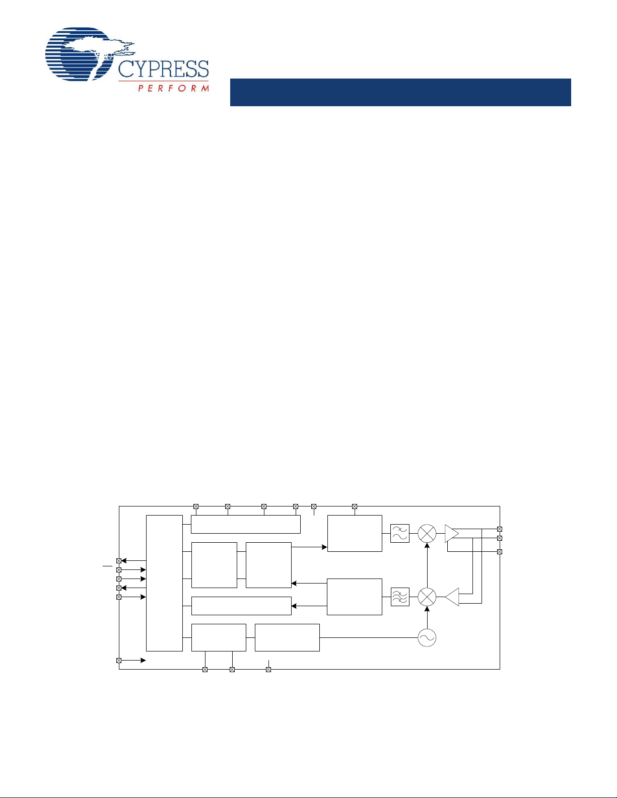
Logic Block Diagram
RF
BIAS
Data
Interface
and
Sequencer
DSSS
Baseband
& Framer
SPI
Synthesizer
GFSK
Demodulator
GFSK
Modulator
IRQ
SS
SCK
MISO
MOSI
RF
P
RF
N
XTAL XOUT
RSSI
Xtal Osc
Power Management
L/D V
DD
V
BAT
V
REG
RST
GND
V
CC
PACTL
■ 2.4 GHz Direct Sequence Spread Spectrum (DSSS) radio
transceiver
■ Operates in the unlicensed worldwide Industria l , Sci en ti f i c,
and Medical (ISM) band (2.400 GHz to 2.483 GHz)
■ 21 mA operating current (Transmit at –5 dBm)
■ Transmit power up to +4 dBm
■ Receive sensitivity up to –97 dBm
■ Sleep Current less than 1 μA
■ DSSS data rates up to 250 kbps, GFSK data rate of 1 Mbps
■ Low external component count
■ Auto Transaction Sequencer (ATS) - no MCU intervention
■ Framing, Length, CRC16, and Auto ACK
■ Power Management Unit (PMU) for MCU/Sensor
■ Fast Startup and Fast Channel Changes
■ Separate 16-byte Transmit and Receive FIFOs
■ AutoRate™ - dynamic data rate reception
■ Receive Signal Strength Indication (RSSI)
■ Serial Peripheral Interface (SPI) control while in sleep mode
■ 4 MHz SPI microcontroller interface
■ Battery Voltage Monitoring Circuitry
■ Supports coin-cell operated applications
■ Operating voltage from 1.8 V to 3.6 V
■ Operating temperature from 0 to 70°C
■ Space saving 40-pin QFN 6x6 mm package
Applications
■ Wireless Keyboards and Mice
■ Wireless Gamepads
■ Remote Controls
■ Toys
■ VOIP and Wireless Headsets
■ White Goods
■ Consumer Electronics
■ Home Automation
■ Automatic Meter Readers
■ Personal Health and Entertainment
Applications Support
See www.cypress.com for development tools, reference
designs, and application notes.
Cypress Semiconductor Corporation • 198 Champion Court • San Jose, CA 95134-1709 • 408-943-2600
Document #: 38-16015 Rev. *J Revised April 18, 2011
[+] Feedback
Page 2

CYRF6936
Contents
Functional Description ...................................... ...............3
Functional Overview ........................................................4
Data Transmission Modes ...........................................4
Link Layer Modes ........................................................4
Packet Buffers .............................................................5
Auto Transaction Sequencer (ATS) ............................5
Data Rates ..................................................................6
Functional Block Overview ............................................. .6
2.4 GHz Radio ................................ ... ..........................6
Frequency Synthesizer ................................................6
Baseband and Framer ........................................ ... ......6
Packet Buffers and Radio Configuration Registers .....6
SPI Interface ................................................................6
Interrupts ..................................................................... 8
Clocks ..........................................................................8
Power Management ....................................................8
Low Noise Amplifier and Received
Signal Strength Indication ............................................8
Receive Spurious Response .......................................9
Application Examples ......................................................9
Registers .........................................................................14
Absolute Maximum Ratings ...........................................15
Operating Conditions .....................................................15
DC Characteristics ..........................................................15
AC Characteristics
RF Characteristics ..........................................................17
Typical Operating Characteristics .................................19
Ordering Information ................................ ... ...................22
Ordering Code Definitions .........................................22
Package Description ......................................................23
Acronyms ........................................................................25
Document Conventions .................................................25
Units of Measure .......................................................25
Document History Page .................................................26
Sales, Solutions, and Legal Information ......................28
Worldwide Sales and Design Support .......................28
Products ....................................................................28
PSoC Solutions .........................................................28
..........................................................16
Document #: 38-16015 Rev. *J Page 2 of 28
[+] Feedback
Page 3
CYRF6936
Functional Description
RF
BIAS
NC
NC
V
BAT2
V
CC
V
BAT1
XTAL
V
CC
NC
NC
V
REG
NC
NC
V
BAT0
L/D
NC
NC
V
I/O
V
DD
RST
RF
N
NCNCVCCNCNCRESV
NC
GND
RF
P
NC
SS
SCK
IRQ / GPIO
MOSI / SDAT
MISO / GPIO
XOUT / GPIO
PACTL / GPIO
NC
NC
* E-PAD Bottom Side
21
22
23
24
25
26
27
28
29
30
11
12131415161718
19
20
10
9
8
7
6
5
4
3
2
40
39383736353433
32
31
1
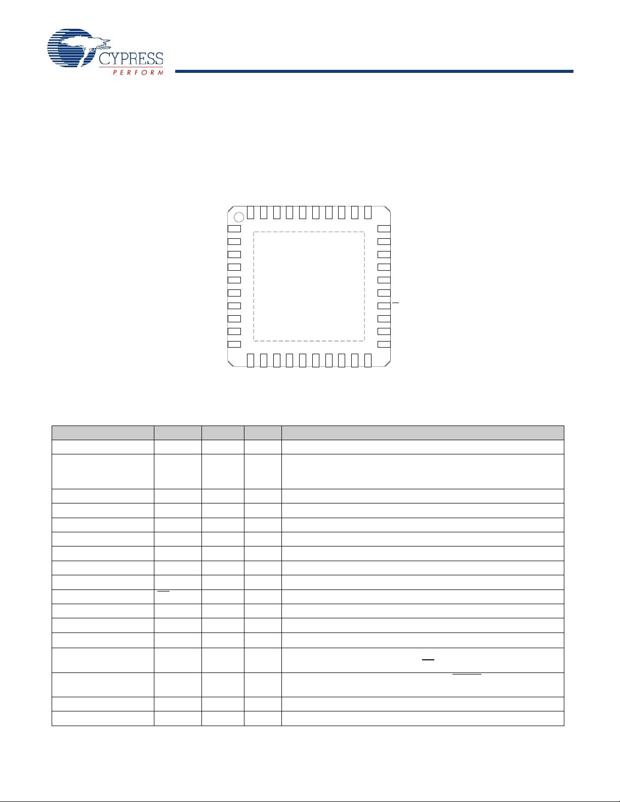
CYRF6936
WirelessUSB LP
40-Pin QFN
Corner
tabs
The CYRF6936 WirelessUSB™ LP radio is a second generation member of the Cypress WirelessUSB Radio System-On-Chip
(SoC) family. The CYRF6936 is interoperable with the first generation CYWUSB69xx devices. The CYRF6936 IC adds a range
of enhanced features, including increased operating voltage range, reduced supply current in all operating modes, higher data
rate options, reduced crystal start up, synthesizer settling, and link turnaround times.
Figure 1. Pin Diagram - CYRF6936 40 QFN
Table 1. Pin Description
Pin Number Name Type Default Description
1 XTAL I I 12 MHz crystal.
2, 4, 5, 9, 14, 15, 17, 18,
NC NC Connect to GND.
20, 21, 22, 23, 31, 32,
36, 39
3, 7, 16 V
6, 8, 38 V
10 RF
11 RF
CC
BAT(0-2)
BIAS
P
Pwr VCC = 2.4 V to 3.6 V. Typically connected to V
Pwr V
= 1.8 V to 3.6 V. Main supply.
BAT
O O RF I/O 1.8 V reference voltage.
I/O I Differential RF signal to and from antenna.
REG.
12 GND GND Ground.
13 RF
N
I/O I Differential RF signal to and from antenna.
19 RESV I Must be connected to GND.
24 SS I I SPI enable, active LOW assertion. Enables and frames transfers.
25 SCK I I SPI clock.
26 IRQ I/O O Interrupt output (configurable active HIGH or LOW), or GPIO.
27 MOSI I/O I
28 MISO I/O Z SPI data output pin (Master In Slave Out), or GPIO (in SPI 3-pin mode).
29 XOUT I/O O Buffered 0.75, 1.5, 3, 6, or 12 MHz clock, PACTL, or GPIO.
Document #: 38-16015 Rev. *J Page 3 of 28
30 PACTL I/O O Control signal for external PA, T/R switch, or GPIO.
33 V
Pwr I/O interface voltage, 1.8–3.6 V.
I/O
SPI data input pin (Master Out Slave In), or SDAT.
Tri-states when SPI 3PIN = 0 and SS
is deasserted.
Tri-states in sleep mode (configure as GPIO drive LOW).
[+] Feedback
Page 4
CYRF6936
Table 1. Pin Description (continued)
Pin Number Name Type Default Description
34 RST I I Device reset. Internal 10 kohm pull down resistor. Active HIGH,
connect through a 0.47 μF capacitor to V
the first time power is applied to the radio. Otherwise the state of the
radio control registers is unknown.
35 V
37 L/D O PMU inductor/diode connection, when used. If not used, connect to
40 V
E-PAD GND GND Must be soldered to Ground.
Corner Tabs NC NC Do Not solder the tabs and keep other signal traces clear. All tabs are
DD
REG
Pwr Decoupling pin for 1.8 V logic regulator, connect through a 0.47 μF
capacitor to GND.
GND.
Pwr PMU boosted output voltage feedback.
common to the lead frame or paddle which is grounded after the pad
is grounded. While they are visible to the user, they do not extend to
the bottom.
Must have RST = 1 event
BAT.
Functional Overview
The CYRF6936 IC provides a complete WirelessUSB SPI to
antenna wireless MODEMs. The SoC is designed to implement
wireless device links operating in the worldwide 2.4 GHz ISM
frequency band. It is intended for systems compliant with
worldwide regulations covered by ETSI EN 301 489-1 V1.41,
ETSI EN 300 328-1 V1.3.1 (Europe), FCC CFR 47 Part 15 (USA
and Industry Canada), and TELEC ARIB_T66_March, 2003
(Japan).
The SoC contains a 2.4 GHz, 1 Mbps GFSK radio transceiver,
packet data buffering, packet framer , DSSS baseband controller,
Received Signal Strength Indication (RSSI), and SPI interface
for data transfer and device configuration.
The radio supports 98 discrete 1 MHz channels (regulations may
limit the use of some of these channels in certain jurisdictions).
The baseband performs DSSS spreading/despreading, Start of
Packet (SOP), End of Packet (EOP) detection, and CRC16
generation and checking. The baseband may also be configured
to automatically transmit Acknowledge (ACK) handshake
packets whenever a valid packet is received.
When in receive mode, with packet framing enabled, the device
is always ready to receive data transmitted at any of the
supported bit rates. This enables the implementation of
mixed-rate systems in which different devices use different data
rates. This also enables the implementation of dynamic data rate
systems that use high data rates at shorter distances or in a
low-moderate interference environment or both. It changes to
lower data rates at longer distances or in high interference
environments or both.
In addition, the CYRF6936 IC has a Power Management Unit
(PMU), which enables direct connection of the device to any
battery voltage in the range 1.8 V to 3.6 V. The PMU conditions
the battery voltage to provide the supply voltages required by the
device, and may supply external devices.
Data Transmission Modes
The SoC supports four different data transmission modes:
■ In GFSK mode, data is transmitted at 1 Mbps, without any
DSSS.
■ In 8DR mode, eight bits are encoded in each derived code
symbol transmitted.
■ In DDR mode, two bits are encoded in each derived code
symbol transmitted (As in the CYWUSB6934 DDR mode).
■ In SDR mode, one bit is encoded in each derived code symbol
transmitted (As in the CYWUSB6934 standard modes).
Both 64 chip and 32 chip Pseudo Noise (PN) codes are
supported. The four data transmission modes apply to the data
after the SOP. In particular the length, data, and CRC16 are all
sent in the same mode. In general, lower data rates reduce
packet error rate in any given environment.
Link Layer Modes
The CYRF6936 IC device supports the following data packet
framing features:
SOP
Packets begin with a two-symbol SoP marker. This is required in
GFSK and 8DR modes, but is optional in DDR mode and is not
supported in SDR mode. If framing is disabled then an SOP
event is inferred whenever two successive correlations are
detected. The SOP_CODE_ADR code used for the SOP is
different from that used for the “body” of the packet, and if desired
may be a different length. SOP must be configured to be the
same length on both sides of the link.
Length
There are two options for detecting the end of a packet. If SOP
is enabled, then the length field must be enabled. GFSK and
8DR must enable the length field. This is the first eight bits after
the SOP symbol, and is transmitted at the payload data rate.
When the length field is enabled, an EoP condition is inferred
after reception of the number of bytes defined in the length field,
plus two bytes for the CRC16. The alternative to using the length
Document #: 38-16015 Rev. *J Page 4 of 28
[+] Feedback
Page 5
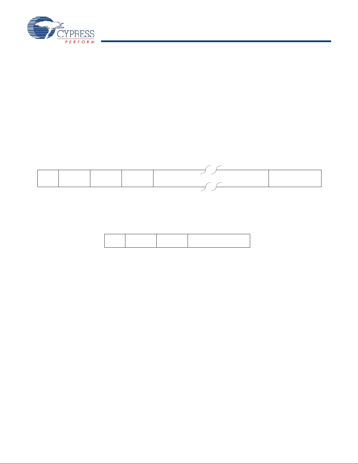
CYRF6936
field is to infer an EOP condition from a configurable number of
P SOP 1 SOP 2 Length CRC 16
Payload Data
Preamble
n x 16us
1st Framing
Sym bol*
2nd Framing
Sym bol*
Packet
length
1 Byte
Period
*Note:32 or 64us
P SOP 1 SOP 2 CRC 16
Preamble
n x 16us
1st Framing
Symbol*
2nd Framing
Sym bol*
CR C field from
received packet.
2 Byte periods
*Note:32 or 64us
successive noncorrelations; this option is not available in GFSK
mode and is only recommended when using SDR mode.
CRC16
The device may be configured to append a 16 bit CRC16 to each
packet. The CRC16 uses the USB CRC polynomial with the
added programmability of the seed. If enabled, the receiver
verifies the calculated CRC16 for the payload data against the
received value in the CRC16 field. The seed value for the CRC16
calculation is configurable, and the CRC16 transmitted may be
calculated using either the loaded seed value or a zero seed; the
received data CRC16 is checked against both the configured
and zero CRC16 seeds.
Figure 2. Example Packet Format
Figure 3. Example ACK Packet Format
CRC16 detects the following errors:
■ Any one bit in error.
■ Any two bits in error (irrespective of how far apart, which
column, and so on).
■ Any odd number of bits in error (irrespective of the location).
■ An error burst as wide as the checksum itself.
Figure 2 shows an example packet with SOP, CRC16, and
lengths fields enabled, and Figure 3 shows a standard ACK
packet.
Packet Buffers
All data transmission and reception use the 16 byte packet
buffers - one for transmission and one for reception.
The transmit buffer allows loading a complete packet of up to 16
bytes of payload data in one burst SPI transaction. This is then
transmitted with no further MCU intervention. Similarly, the
receive buffer allows receiving an entire packet of payload data
up to 16 bytes with no firmware intervention required until the
packet reception is complete.
The CYRF6936 IC supports packets up to 255 bytes. However,
the actual maximum packet length depends on the accuracy of
the clock on each end of the link and the data mode. Interrupts
are provided to allow an MCU to use the transmit and receive
buffers as FIFOs. When transmitting a packet longer than 16
bytes, the MCU can load 16 bytes initially, and add further bytes
to the transmit buffer as transmission of data creates space in
the buffer. Similarly, when receiving packets longer than 16
bytes, the MCU must fetch received data from the FIFO
periodically during packet reception to prevent it from
overflowing.
Auto Transaction Sequencer (ATS)
The CYRF6936 IC provides automated support for transmission
and reception of acknowledged data packets.
When transmitting in transaction mode, the device automatically:
■ starts the crystal and synthesizer
■ enters transmit mode
■ transmits the packet in the transmit buffer
■ transitions to receive mode and waits for an ACK packet
■ transitions to the transaction end state when an ACK packet is
received or a timeout period expires
Similarly, when receiving in transaction mode, the device
automatically:
■ waits in receive mode for a valid packet to be received
■ transitions to transmit mode, transmits an ACK packet
■ transitions to the transaction end state (receive mode to await
the next packet, and so on.)
The contents of the packet buffers are not affected by the
transmission or reception of ACK packets.
Document #: 38-16015 Rev. *J Page 5 of 28
[+] Feedback
Page 6
CYRF6936
In each case, the entire packet transaction takes place without
any need for MCU firmware action (as long as packets of 16
bytes or less are used). T o transmit data, the MCU must load the
data packet to be transmitted, set the length, and set the TX GO
bit. Similarly, when receiving packets in transaction mode,
firmware must retrieve the fully received packet in response to
an interrupt request indicating reception of a packet.
Data Rates
The CYRF6936 IC supports the following data rates by
combining the PN code lengths and data transmission modes
described in the previous sections:
■ 1000 kbps (GFSK)
■ 250 kbps (32 chip 8DR)
■ 125 kbps (64 chip 8DR)
■ 62.5 kbps (32 chip DDR)
■ 31.25 kbps (64 chip DDR)
■ 15.625 kbps (64 chip SDR)
Functional Block Overview
2.4 GHz Radio
The radio transceiver is a dual conversion low IF architecture
optimized for power, range, and robustness. The radio employs
channel-matched filters to achieve high performance in the
presence of interference. An integrated Power Amplifier (PA)
provides up to +4 dBm transmit power, with an output power
control range of 34 dB in seven steps. The supply current of the
device is reduced as the RF output power is reduced.
Table 2. Internal PA Output Power Step Table
PA Setting Typical Output Power (dBm)
7+4
60
5–5
4–13
3–18
2–24
1–30
0–35
Frequency Synthesizer
Before transmission or reception may begin, the frequency
synthesizer must settle. The settling time varies depending on
channel; 25 fast channels are provided with a maximum settling
time of 100 μs.
The ‘fast channels’ (less than 100 μs settling time) are every third
channel, starting at 0 up to and including 72 (for example, 0, 3,
6, 9 …. 69, 72).
Baseband and Framer
The baseband and framer blocks provide the DSSS encoding
and decoding, SOP generation and reception, CRC16
generation and checking, and EOP detection and length field.
Packet Buffers and Radio Configuration Registers
Packet data and configuration registers are accessed through
the SPI interface. All configuration registers are directly
addressed through the address field in the SPI packet (as in the
CYWUSB6934). Configuration registers allow configuration of
DSSS PN codes, data rate, operating mode, interrupt masks,
interrupt status, and so on.
SPI Interface
The CYRF6936 IC has an SPI interface supporting
communication between an application MCU and one or more
slave devices (including the CYRF6936). The SPI interface
supports single-byte and multi-byte serial transfers using either
4-pin or 3-pin interfacing. The SPI communications interface
consists of Slave Select (SS
Out-Slave In (MOSI), Master In-Slave Out (MISO), or Serial Data
(SDAT).
SPI communication may be described as the following:
■ Command Direction (bit 7) = ‘1’ enables SPI write transaction.
A ‘0’ enables SPI read transactions.
■ Command Increment (bit 6) = ‘1’ enables SPI auto address
increment. When set, the address field automatically
increments at the end of each data byte in a burst access.
Otherwise the same address is accessed.
■ Six bits of address
■ Eight bits of data
The device receives SCK from an application MCU on the SCK
pin. Data from the application MCU is shifted in on the MOSI pin.
Data to the application MCU is shifted out on the MISO pin. The
active LOW Slave Select (SS
SPI transfer.
The application MCU can initiate SPI data transfers using a
multi-byte transaction. The first byte is the Command/Address
byte, and the following bytes are the data bytes shown in Table 3
through Figure 6 on page 7.
The SPI communications interface has a burst mechanism,
where the first byte can be followed by as many data bytes as
required. A burst transaction is terminated by deasserting the
slave select (SS
= 1).
The SPI communications interface single read and burst read
sequences are shown in Figure 4 and Figure 5 on page 7,
respectively.
The SPI communications interface single write and burst write
sequences are shown in Figure 6 and Figure 7 on page 7,
respectively.
This interface may be optionally operated in a 3-pin mode with
the MISO and MOSI functions combined in a single bidirectional
data pin (SDAT). When using 3-pin mode, user firmware must
ensure that the MOSI pin on the MCU is in a high impedance
state except when MOSI is actively transmitting data.
), Serial Clock (SCK), Master
) pin must be asserted to initiate an
Document #: 38-16015 Rev. *J Page 6 of 28
[+] Feedback
Page 7
CYRF6936
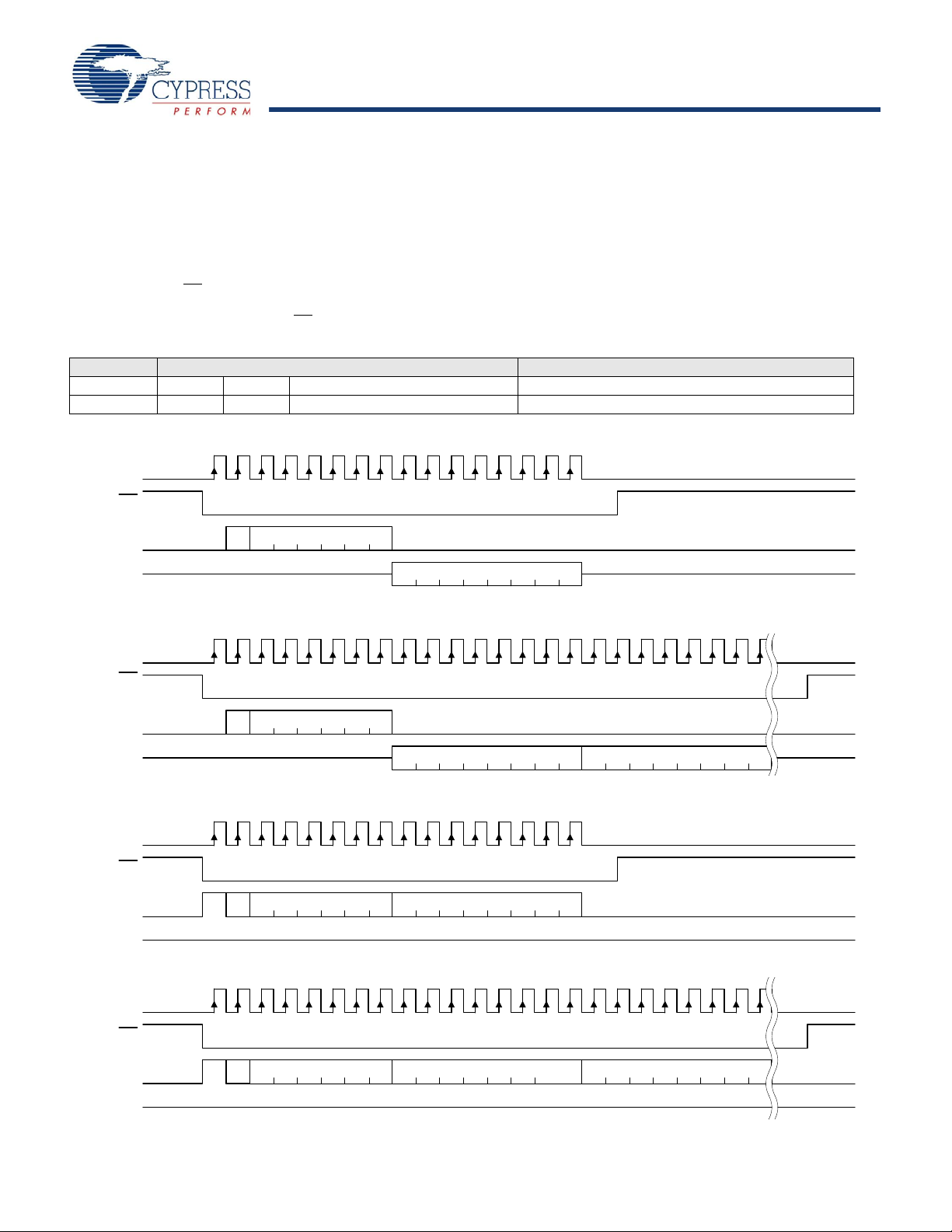
The device registers may be written to or read from one byte at
DIR
0
INCA5A4A3A2A1A0
D7 D6 D5 D4 D3 D2 D1 D0
SCK
MOSI
SS
MISO
cmd addr
data to mcu
DIR
0
INCA5A4A3A2A1A0
D7 D6 D5 D4 D3 D2 D1 D0 D7 D6 D5 D4 D3 D2 D1 D0
data to mcu
1
cmd addr
data to mcu
1+N
SCK
MOSI
SS
MISO
DIR
1
INCA5A4A3A2A1A0
D7 D6 D5 D4 D3 D2 D1 D0
SCK
MOSI
SS
MISO
cmd addr data from mcu
DIR
1
INCA5A4A3A2A1A0
D7 D6 D5 D4 D3 D2 D1 D0
SCK
MOSI
SS
MISO
cmd addr data from mcu
1
D7 D6 D5 D4 D3 D2 D1 D0
data from mcu
1+N
a time, or several sequential register locations may be written or
read in a single SPI transaction using incrementing burst mode.
In addition to single byte configuration registers, the device
includes register files. Register files are FIFOs written to and
read from using nonincrementing burst SPI transactions.
The IRQ pin function may be optionally multiplexed onto the
The SPI interface is not dependent on the internal 12 MHz clock.
Registers may therefore be read from or written to when the
device is in sleep mode, and the 12 MHz oscillator disabled.
The SPI interface and the IRQ and RST pins have a separate
voltage reference pin (V
directly to MCUs operating at voltages below the CYRF6936 IC
). This enables the device to interface
I/O
supply voltage.
MOSI pin. When this option is enabled, the IRQ function is not
available while the SS pin is LOW. When using this configuration,
user firmware must ensure that the MOSI pin on the MCU is in a
high impedance state whenever the SS pin is HIGH.
Table 3. SPI Transaction Format
Parameter Byte 1 Byte 1+N
Bit # 7 6 [5:0] [7:0]
Bit Name DIR INC Address Data
Figure 4. SPI Single Read Sequence
Figure 5. SPI Incrementing Burst Read Sequence
Figure 6. SPI Single Write Sequence
Figure 7. SPI Incrementing Burst Write Sequence
Document #: 38-16015 Rev. *J Page 7 of 28
[+] Feedback
Page 8

CYRF6936
Interrupts
The device provides an interrupt (IRQ) output, which is
configurable to indicate the occurrence of various different
events. The IRQ pin may be programmed to be either active
HIGH or active LOW, and be either a CMOS or open drain output.
The available interrupts are described in the section Registers
on page 14.
The CYRF6936 IC features three sets of interrupts: transmit,
receive, and system interrupts. These interrupts all share a
single pin (IRQ), but can be independently enabled or disabled.
The contents of the enable registers are preserved when
switching between transmit and receive modes.
If more than one interrupt is enabled at any time, it is necessary
to read the relevant status register to determine which event
caused the IRQ pin to assert. Even when a given interrupt source
is disabled, the status of the condition that would otherwise
cause an interrupt can be determined by reading the appropriate
status register. It is therefore possible to use the devices without
the IRQ pin, by polling the status registers to wait for an event,
rather than using the IRQ pin.
Clocks
A 12 MHz crystal (30 ppm or better) is directly connected
between XTAL and GND without the need for external
capacitors. A digital clock out function is provided, with
selectable output frequencies of 0.75, 1.5, 3, 6, or 12 MHz. This
output may be used to clock an external microcontroller (MCU)
or ASIC. This output is enabled by default, but may be disabled.
The requirements to directly connect the crystal to the XTAL pin
and GND are:
■ Nominal Frequency: 12 MHz
■ Operating Mode: Fundamental Mode
■ Resonance Mode: Parallel Resonant
■ Frequency Stability: ±30 ppm
■ Series Resistance: <60 ohms
■ Load Capacitance: 10 pF
■ Drive Level: 100 µW
Power Management
The operating voltage of the device is 1.8 V to 3.6 V DC, which
is applied to the V
static sleep mode by writing to the FRC END = 1 and
END STA TE = 000 bits in the XACT_CFG_ADR register over the
SPI interface. The device enters sleep mode within 35 µs after
the last SCK positive edge at the end of this SPI transaction.
Alternatively, the device may be configured to automatically
enter sleep mode after completing the packet transmission or
reception. When in sleep mode, the on-chip oscillator is stopped,
but the SPI interface remains functional. The device wakes from
sleep mode automatically when the device is commanded to
enter transmit or receive mode. When resuming from sleep
mode, there is a short delay while the oscillator restarts. The
device can be configured to assert the IRQ pin when the
oscillator has stabilized.
pin. The device can be shut down to a fully
BAT
The output voltage (V
(PMU) is configurable to several minimum values between 2.4 V
and 2.7 V. V
load) to external devices. It is possible to disable the PMU and
may be used to provide up to 15 mA (average
REG
) of the Power Management Unit
REG
provide an externally regulated DC supply voltage to the device’s
main supply in the range 2.4 V to 3.6 V. The PMU also provides
a regulated 1.8 V supply to the logic.
The PMU is designed to provide high boost efficiency (74–85%
depending on input voltage, output voltage, and load) when
using a Schottky diode and power inductor, eliminating the need
for an external boost converter in many systems where other
components require a boosted voltage. However, reasonable
efficiencies (69–82% depending on input voltage, output voltage,
and load) may be achieved when using low cost components
such as SOT23 diodes and 0805 inductors.
The current through the diode must stay within the linear
operating range of the diode. For some loads the SOT23 diode
is sufficient, but with higher loads it is not and an SS12 diode
must be used to stay within this linear range of operation. Along
with the diode, the inductor used must not saturate its core. In
higher loads, a lower resistance/higher saturation coil such as
the inductor from Sumida must be used.
The PMU also provides a configurable low battery detection
function, which may be read over the SPI interface. One of seven
thresholds between 1.8 V and 2.7 V may be selected. The
interrupt pin may be configured to assert when the voltage on the
V
pin falls below the configured threshold. LV IRQ is not a
BAT
latched event. Battery monitoring is disabled when the device is
in sleep mode.
Low Noise Amplifier and Received Signal Strength
Indication
The gain of the receiver can be controlled directly by clearing the
AGC EN bit and writing to the Low Noise Amplifier (LNA) bit of
the RX_CFG_ADR register. Clearing the LNA bit reduces the
receiver gain approximately 20 dB, allowing accurate reception
of very strong received signals (for example, when operating a
receiver very close to the transmitter). Approximately 30 dB of
receiver attenuation can be added by setting the Attenuation
(ATT) bit. This limits data reception to devices at very short
ranges. Disabling AGC and enabling LNA is recommended,
unless receiving from a device using external PA.
When the device is in receive mode the RSSI_ADR register
returns the relative signal strength of the on-channel signal
power.
When receiving, the device automatically measures and stores
the relative strength of the signal being received as a five bit
value. An RSSI reading is taken automatically when the SoP is
detected. In addition, a new RSSI reading is taken every time the
previous reading is read from the RSSI_ADR register, allowing
the background RF energy level on any given channel to be
easily measured when RSSI is read while no signal is being
received. A new reading can occur as fast as once every 12 µs.
Document #: 38-16015 Rev. *J Page 8 of 28
[+] Feedback
Page 9
CYRF6936
Receive Spurious Response
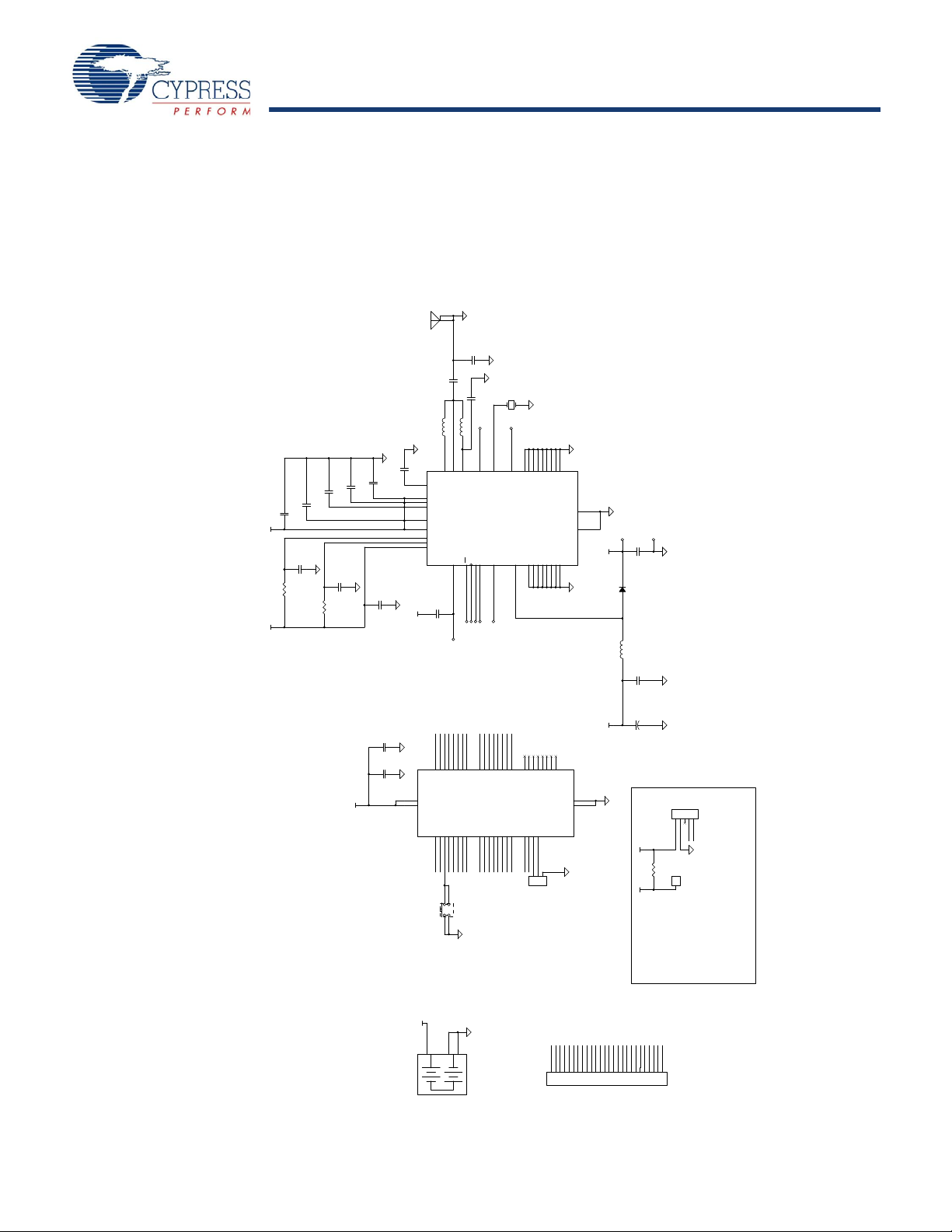
Keyboard Interface
Power Supply
SDATA
ISSP
SCLK
"-"
XRES
"+"
BIND
Serial debug
header
Layout J3 and J2.1 in a
0.100" spacing
configuration
E-PAD must be soldered to ground.
Radio Decoupling Caps
RF VCO
and VCO
Buffer
Filter
The power supply decoupling shown for VBAT0
is a recommended cost effective
configuration:
C6=No Load R2= 1ohm C7=10uF ceramic.
For this configuration, it is required that
C18 be installed.
An alternate decoupling configuration is
the following:
C6=47uF ceramic R2=0ohm C7=.047uF.
For this configuration, it is not required
to load C18.
For reference design part numbers, please
refer to the Bill of Materials file
121-26504_A.xls.
A 2-pin jumper
installed from J3.1
to J2.1 enables the
radio to power the
processor. Jumper
removal is required
when programming U2
to disconnect the
radio from the
Miniprog 5V source.
R1 is a zero ohm
resistor that should
be installed for
production units
only, following
programming.
MISO
MOSI
P1_1
SCK
P1_0
MISO
nSS
IRQ
MOSI
CLKOUT
RST
SCK
COL16
COL10
COL17
COL9
COL13
P1_0
COL15
COL18
COL12
COL11
COL14
nSS
P1_1
COL5
COL3
COL2
COL8
COL1
COL6
COL7
COL4
ROW5
ROW4
ROW6
ROW2
ROW7
ROW1
ROW8
ROW3
COL7
COL11
ROW4
ROW2
COL1
COL3
COL8
COL10
COL14
ROW8
ROW3
COL2
COL6
ROW6
ROW5
COL18
ROW1
COL13
COL16
COL9
ROW7
COL5
COL4
COL12
COL15
COL17
IRQ
SW1
PACTL
EVCC
VCC
VBAT
VBAT
VCC
VBAT
VBAT
VCC
EVCC
SOT23
D1
BAT400D
2 1
IND0402
L2
1.8 nH
U2
CY7C60123-PVXC
30
161718
292826
25
19
23
12
5
7
24
10
2043214222
6
34353637383940
41
131415
313233
2744
1198412346474845
P1_4 / SCLK
P0_7
P0_6 / TIO1
P0_5 / TIO0
P1_3 / SSEL
P1_2
P1_1
P1_0
P0_4 / INT2
P0_0 / CLKIN
P2_3
VDD1
P4_0
VSS1
P2_5
P0_3 / INT1
P4_3
P0_2 / INT0
P4_2
P0_1 / CLKOUT
P4_1
P3_0
P3_1
P3_2
P3_3
P3_4
P3_5
P3_6
P3_7
P2_2
P2_1
P2_0
P1_5 / SMOSI
P1_6 / SMISO
P1_7
VDD2VSS2
P2_4
P2_6
P2_7
NC4
NC1
NC2
NC3
NC6
NC7
NC8
NC5
S1
SW PUSHBUTTON
1A
2A
1B
2B
0402
C5
0.47 uFd
IND0603
L1
22 nH
0603
R1
NO LOAD
J1
KB 26 Pin
12345678910111213141516171819202122232425
26
123456789
1011121314151617181920212223242526
TV4
0402
C8
1 uFd 6.3V
BH1
BATT CON 2xAA
123
POS
NEG1
NEG2
0402
C11
0.047 uFd
0402
C17
0.47 uFd
0805
R2
1 1%
L3
10 uH
TV5
0805
C12
10 uFd 6.3V
0805
C7
10 uFd 6.3V
0402
C20
0.01 uFd
0402
C16
0.047 uFd
J3
1 PIN HDR
1
TV8
J2
5 PIN HDR
12345
J4
3 PIN HDR
123
0402
R3
47
TP2
TP1
0402
C13
0.047 uFd
U1
CYRF6936
36
4
8
1916202
252726
29
34
28
3
7
5
13
6
37
1
24
39
40
41
35
9
14
10
11
12
151718
21302233233132
38
NC15
NC2
VBAT2
RESV
VCC3
NC9NC1
SCK
MOSI
IRQ
XOUT
RST
MISO
VCC1
VCC2
NC3
RFn
VBAT1
L/D
XTAL
SS
NC16
VREG
E-PAD
VDD
NC4
NC5
RFbias
RFp
GND1
NC6
NC7
NC8
NC10
PACTL
NC11
VIO
NC12
NC13
NC14
VBAT0
0402
C3
2.0 pFd
0402
C1
15 pFd
+
E
C18
100 uFd 10v
0402
C15
0.047 uFd
TV7
TV6
ANT1
WIGGLE 63
1
2
0402
C4
1.5 pFd
Y1
12 MHz Crystal
TV2
1210
C6
No Load
0402
C10
0.047 uFd
TV1
TV3
0402
C19
0.01 uFd
0402
C9
0.047 uFd
The transmitter may exhibit spurs around 50MHz offset at levels
approximately 50dB to 60dB below the carrier power. Receivers
operating at the transmit spur frequency may receive the spur if
the spur level power is greater than the receive sensitivity level.
Application Examples
The workaround for this is to program an additional byte in the
packet header which contains the transmitter channel number.
After the packet is received, the channel number can be
checked. If the channel number does not match the receive
channel then the packet is rejected.
Figure 8. Recommended Circuit for Systems where VBAT
≤ 2.4 V
Document #: 38-16015 Rev. *J Page 9 of 28
[+] Feedback
Page 10

CYRF6936
Table 4. Recommended BoM for Systems where VBAT ≤ 2.4 V
Item Qty CY Part Number Reference Description Manufacturer Mfr Part Number
1 1 NA ANT1 2.5GHZ H-STUB WIGGLE
ANTENNA FOR 63MIL PCB
2 1 NA BH1 BATTERY CLIPS 2AA CELL
3 1 730-10012 C1 CAP 15PF 50 V CERAMIC NPO
4 1 730-11955 C3 CAP 2.0 PF 50 V CERAMIC NPO
5 1 730-11398 C4 CAP 1.5PF 50 V CERAMIC NPO
6 2 730R-13322 C5,C17 CAP CER .47UF 6.3 V X5R 0402 Murata GRM155R 60J474KE19D
7 2 730-13037 C12,C7 CAP CERAMIC 10UF 6.3 V X5R
8 1 730-13400 C8 CAP 1 uF 6.3 V CERAMIC X5R
9 6 730-13404 C9,C10,C11,
C13,C15,C16
10 1 710-13201 C18 CAP 100UF 10 V ELECT FC Panasonic - ECG EEU-FC1A101S
11 2 730-10794 C20,C19 CAP 10000PF 16 V CERAMIC
12 1 800-13317 D1 DIODE SCHOTTKY 0.5A 40 V
13 1 NA J1 PCB COPPER PADS NONE
14 1 420-11496 J2 CONN HDR BRKWAY 5POS STR
15 1 420-11964 J3 HEADER 1 POS 0.230 HT MODII
16 1 800-13401 L1 INDUCTOR 22NH 2% FIXED 0603
17 1 800-116 51 L2 INDUCTOR 1.8NH +-.3NH FIXED
18 1 800-10594 L3 COIL 10UH 1100MA CHOKE 0805 Newark 30K5421
19 1 630-11356 R2 RES 1.00 OHM 1/8W 1% 0805
20 1 610-13402 R3 RES 47 OHM 1/16W 5% 0402 SMD Panasonic - ECG ERJ-2GEJ470X
21 1 800-13368 S1 LT SWITCH 6MM 100GF H=7MM THPanasonic - ECG EVQ-PAC07K
0402
0402
0402 SMD
0805
0402
CAP 0.047 uF 16 V CERAMIC X5R
0402
0402 SMD
SOT23
AU PCB
.100CL
SMD
0402 SMD
SMD
NA NA
Panasonic ECJ-0EC1H150J
Kemet C0402C209C5GACTU
PANASONIC ECJ-0EC1H1R5C
Kemet C0805C106K9PACTU
Panasonic ECJ-0EB0J105M
AVX 0402YD473KAT2A
Panasonic - ECG ECJ-0EB1C103K
DIODES INC BAT400D-7-F
AMP Division of
TYCO
AMP/Tyco 103185-1
Panasonic - ECG ELJ-RE22NGF2
Panasonic - ECG ELJ-RF1N8DF
Yageo 9C08052A1R00FKHFT
103185-5
22 1 CYRF6936-40LFCU1 IC, LP 2.4 GHz RADIO SoC
QFN-40
23 1 CY7C60123-PVXCU2 IC WIRELESS EnCore II
CONTROLLER SSOP48
24 1 800-13259 Y1 CRYSTAL 12.00MHZ HC49 SMD eCERA GF-1200008
25 1 PDC-9265-*B PCB PRINTED CIRCUIT BOARD Cypress
26 1 920-11206 LABEL1 Serial Number
27 1 920-26504 *A LABEL2 PCA # 121-26504 *A
Document #: 38-16015 Rev. *J Page 10 of 28
Cypress
Semiconductor
Cypress
Semiconductor
Semiconductor
CYRF6936 Rev A5
CY7C60123-PVXC
PDC-9265-*B
[+] Feedback
Page 11

CYRF6936
Table 4. Recommended BoM for Systems where VBAT ≤ 2.4 V (continued)
Item Qty CY Part Number Reference Description Manufacturer Mfr Part Number
No Load Components - Do Not Install
28 1 730-13403 C6 CAP 47UF 6.3 V CERAMIC X5R
1210
29 1 630-10242 R2 RES CHIP 0.0 OHM 1/10W 5%
0805 SMD
30 1 730-13404 C7 CAP 0.047 uF 50 V CERAMIC X5R
0402
31 1 420-10921 J4 HEADER 3POS FRIC STRGHT
MTA 100
32 1 620-10519 R1 RES ZERO OHM 1/16W 5% 0603
SMD
Panasonic ECJ-4YB0J476M
Phycomp USA Inc 9C08052A0R00JLHFT
AVX 0402YD473KAT2A
AMP/Tyco 644456-3
Panasonic - ECG ERJ-3GEY0R00V
Document #: 38-16015 Rev. *J Page 11 of 28
[+] Feedback
Page 12

CYRF6936
DP
SW1
VBUS
DM
nSS
SCK
MISO
MOSI
IRQ
SW1
nLED1
nLED2
RST
nLED1
nLED2
IRQ
RST
MOSI
SCK
nSS
MISO
5V
5V
VCC
VCC
5V
VCC
VCC
5V
VCC
"BIND"
Power Supply
"CONNECT/ACTIVITY"
E-PAD must be soldered to ground.
U1
CYRF6936U1CYRF6936
NC15
36
NC2
4
VBAT2
8
RESV
19
VCC3
16
NC9
20
NC1
2
SCK25MOSI27IRQ
26
XOUT
29
RST34MISO
28
VCC1
3
VCC2
7
NC3
5
RFn
13
VBAT1
6
L/D
37
XTAL
1
SS
24
NC16
39
VREG
40
E-PAD
41
VDD
35
NC49NC5
14
RFbias
10
RFp
11
GND1
12
NC615NC717NC8
18
NC10
21
PACTL
30
NC11
22
VIO
33
NC1223NC1331NC14
32
VBAT0
38
IND0402
L2
1.8 nH
IND0402
L2
1.8 nH
0402
C9
0.047 uFd
0402
C9
0.047 uFd
J1
USB A SMT PLUG
J1
USB A SMT PLUG
VBUS
1
DM
2
DP
3
GND
4
S15S2
6
0402
C1
15 pFd
0402
C1
15 pFd
D1
LED Green Red
D1
LED Green Red
GR1RD
2
C3C
4
0402
R1
zero
0402
R1
zero
0402
R2
620
0402
R2
620
ANT1
WIGGLE 32
ANT1
WIGGLE 32
1
2
0402
C12
1500 pFd
0402
C12
1500 pFd
0402
C10
0.047 uFd
0402
C10
0.047 uFd
0402
C3
2.0 pFd
0402
C3
2.0 pFd
0402
C7
0.047 uFd
0402
C7
0.047 uFd
0805
C13
4.7 uFd
0805
C13
4.7 uFd
0805
C14
2.2 uFd
0805
C14
2.2 uFd
S1
SW RA PUSH
S1
SW RA PUSH
1A
1B
2A
2B
0402
C6
0.047 uFd
0402
C6
0.047 uFd
Y1
12 MHz Crystal
Y1
12 MHz Crystal
TV1 TV-20RTV1 TV-20R
0402
C15
0.47 uFd
0402
C15
0.47 uFd
0402
C11
0.047 uFd
0402
C11
0.047 uFd
0402
C4
1.5 pFd
0402
C4
1.5 pFd
0402
C8
0.047 uFd
0402
C8
0.047 uFd
U2
CY7C63803-SXC
U2
CY7C63803-SXC
P0_07P0_1
6
P0_2/INT05P0_3/INT14P0_4/INT2
3
P0_5/TIO02P0_6/TIO1
1
MISO/P1_6
16
MOSI/P1_5
15
VSS
8
VCC
11
VREG
12
DM/P1_110DP/P1_09SSEL/P1_313SCLK/P1_4
14
0402
C5
0.47 uFd
0402
C5
0.47 uFd
IND0603
L1
22 nH
IND0603
L1
22 nH
Figure 9. Recommended Circuit for Systems where V
is 2.4 V - 3.6 V (PMU Disabled)
BAT
Document #: 38-16015 Rev. *J Page 12 of 28
[+] Feedback
Page 13

CYRF6936
Table 5. Recommended BoM for Systems where V
Item Qty CY Part Number Reference Description Manufacturer Mfr Part Number
1 1 NA ANT1 2.5GHZ H-STUB WIGGLE ANTENNA
FOR 32MIL PCB
2 1 730-10012 C1 CAP 15PF 50 V CERAMIC NPO 0402 Panasonic ECJ-0EC1H150J
3 1 730-11955 C3 CAP 2.0 PF 50 V CERAMIC NPO 0402 Kemet C0402C209C5GACTU
4 1 730-11398 C4 CAP 1.5PF 50 V CERAMIC NPO 0402
SMD
5 1 730-13322 C5, C15 CAP 0.47 uF 6.3 V CERAMIC X5R 0402 Murata GRM155R60J474KE19D
6
7 6 730-13404 C6,C7,C8,C
9,C10,C1 1
8 1 730-11953 C12 CAP 1500PF 50 V CERAMIC X7R 0402 Kemet C0402C152K5RACTU
9 1 730-13040 C13 CAP CERAMIC 4.7UF 6.3 V XR5 0805 Kemet C0805C475K9PACTU
10 1 730-12003 C14 CAP CER 2.2UF 10 V 10% X7R 0805 Murata
11 1 800-13333 D1 LED GREEN/RED BICOLOR 1210 SMD LITEON LTST-C155KGJRKT
12 1 420-13046 J1 CONN USB PLUG TYPE A PCB SMT ACON UAR72-4N5J10
13 1 800-13401 L1 I NDUCTOR 22NH 2% FIXED 0603 SMD Panasonic - ECG ELJ-RE22NGF2
14 1 800-11651 L2 INDUCTOR 1.8NH +-.3NH FIXED 0402
15 1 610-10343 R1 RES ZERO OHM 1/16W 0402 SMD Panasonic - ECG ERJ-2GE0R00X
16 1 610-13472 R2 RES CHIP 620 OHM 1/16W 5% 0402
17 1 200-13471 S1 SWITCH LT 3.5MMX2.9MM 160GF SMD Panasonic - ECG EVQ-P7J01K
18 1 CYRF6936-40LFC U1 IC, LP 2.4 GHz RADIO SoC QFN-40 Cypress
19 1 CY7C63803-SXC U2 IC LOW SPEED USB ENCORE II
20 1 800-13259 Y 1 CRYSTAL 12.00MHZ HC49 SMD eCERA GF-1200008
21 1 PDC-9263-*B PCB PRINTED CIRCUIT BOARD Cypress
22 1 LABEL1 Serial Number XXXXXX
23 1 LABEL2 PCA # 121-26305 **
CAP 0.047 uF 16 V CERAMIC X5R 0402 AVX 0402YD473KAT2A
SMD
SMD
CONTROLLER SOIC16
is 2.4 V - 3.6 V (PMU disabled)
BAT
NA NA
PANASONIC ECJ-0EC1H1R5C
GRM21BR71A225KA01L
Electronics North
America
Panasonic - ECG ELJ-RF1N8DF
Panasonic - ECG ERJ-2GEJ621X
CYRF6936 Rev A5
Semiconductor
Cypress
Semiconductor
Semiconductor
CY7C63803-SXC
PDC-9263-*B
Document #: 38-16015 Rev. *J Page 13 of 28
[+] Feedback
Page 14

CYRF6936
Registers
Notes
1. b = read/write; r = read only; w = write only; ‘-’ = not used, default value is undefined.
2. Registers must be configured or accessed only when the radio is in IDLE or SLEEP mode. The PMU, GPIOs, and RSSI registers can be accessed in Active Tx and
Rx mode.
3. PFET Bit: Setting this bit to "1" disables the FET , therefore safely allowing Vbat to be connected to a separate reference fro m Vcc when the PMU is disabled to the radio.
4. EOP_CTRL_ADR[6:4] must never have the value of “000”, that is, EOP Hint Symbol count must never be “0”
5. SOP_CODE_ADR default = 0x17FF9E213690C782.
6. DATA_CODE_ADR default = 0x02F9939702FA5CE3012BF1DB0132BE6F.
7. PREAMBLE_ADR default = 0x333302. The count value must be great than 4 for DDR and greater than 8 for SDR.
All registers are read and writable, except where noted. Registers may be written to or read from individually or in sequential groups.
Table 6. Register Map Summary
Address Mnemonic b7 b6 b5 b4 b3 b2 b1 b0 Default
0x00 CHANNEL_ADR Not Used Channel -1001000 -bbbbbbb
0x01 TX_LENGTH_ADR TX Length 00000000 bbbbbbbb
0x02 TX_CTRL_ADR TX GO TX CLR
0x03 TX_CFG_ADR Not Used Not Used
0x04 TX_IRQ_STATUS_ADR
0x05 RX_CTRL_ADR RX GO RSVD
0x06
0x07 RX_IRQ_STATUS_ADR
0x08 RX_STATUS_ADR RX ACK PKT ERR EOP ERR CRC0 Bad CRC RX Code RX Data Mode -------- rrrrrrrr
0x09 RX_COUNT_ADR RX Count 00000000 rrrrrrrr
0x0A RX_LENGTH_ADR RX Length 00000000 rrrrrrrr
[1]
0x0B
0x0C XTAL_CTRL_ADR XOUT FN XSIRQ EN Not Used Not Used FREQ 000--100 bbb--bbb
0x0D IO_CFG_ADR IRQ OD IRQ POL MISO OD XOUT OD PACTL OD PACTL
0x0E GPIO_CTRL_ADR XOUT OP MISO OP PACTL OP IRQ OP XOUT IP MISO IP PACTL IP IRQ IP 0000---- bbbbrrrr
0x0F XACT_CFG_ADR ACK EN Not Used FRC END END STATE ACK TO 1-0000 00 b-bbbbbb
0x10 FRAMING_CFG_ADR SOP EN SOP LEN LEN EN SOP TH 10100101 bbbbbbbb
0x11 DATA32_THOLD_ADR Not Used Not Used Not Used Not Used TH32 ----0100 ----bbbb
0x12 DATA64_THOLD_ADR Not Used Not Used Not Used TH64 ---01010 ---bbbbb
0x13 RSSI_ADR SOP Not Used LNA RSSI 0-100000 r-rrrrrr
0x14
0x15 CRC_SEED_LSB_ADR CRC SEED LSB 00000000 bbbbbbbb
0x16 CRC_SEED_MSB_ADR CRC SEED MSB 00000000 bbbbbbbb
0x17 TX_CRC_LSB_ADR CRC LSB -------- rrrrrrrr
0x18 TX_CRC_MSB_ADR CRC MSB -------- rrrrrrrr
0x19 RX_CRC_LSB_ADR CRC LSB 11111111 rrrrrrrr
0x1A RX_CRC_MSB_ ADR CRC MSB 11111111 rrrrrrrr
0x1B TX_OFFSET_LSB_ADR STRIM LSB 00000000 bbbbbbbb
0x1C TX_OFFSET_MSB_ADR Not Used Not Used Not Used Not Used STRIM MSB ----0000 ----bbbb
0x1D MODE_OVERRIDE_ADR RSVD RSVD FRC SEN FRC AWAKE Not Used Not Used RST 00000--0 wwwww--w
0x1E RX_OVERRIDE_ADR ACK RX RXTX DLY MAN RXACK
0x1F TX_OVERRIDE_ADR ACK TX FRC PRE RSVD
0x26 XTAL_CFG_ADR RSVD RSVD RSVD RSVD START DLY RSVD RSVD RSVD 00000000 wwwwwwww
0x27 CLK_OVERRIDE_ADR RSVD RSVD RSVD RSVD RSVD RSVD RXF RSVD 00000000 wwwwwwww
0x28 CLK_EN_ADR RSVD RSVD RSVD RSVD RSVD RSVD RXF RSVD 00000000 wwwwwwww
0x29 RX_ABORT_ADR RSVD RSVD ABORT EN RSVD RSVD RSVD RSVD RSVD 00000000 wwwwwwww
0x32 AUTO_CAL_TIME_ADR AUTO_CAL_TIME 00000011 wwwwwwww
0x35 AUTO_CAL_OFFSET_ADR AUTO_CAL_OFFSET 00000000 wwwwwwww
0x39 ANALOG_CTRL_ADR RSVD RSVD RSVD RSVD RSVD RSVD RX INV ALL SLOW 00000000 wwwwwwww
Register Files
0x20 TX_BUFFER_ADR TX Buffer File -------- wwwwwwww
0x21 RX_BUFFER_ADR RX Buffer File -------- rrrrrrrr
0x22 SOP_CODE_ADR SOP Cod e File Note 5 bbbbbbbb
0x23 DATA_CODE_ADR Data Code File Note 6 bbbbbbbb
0x24 PREAMBLE_ADR Preamble File Note 7 bbbbbbbb
0x25 MFG_ID_ADR MFG ID File NA rrrrrrrr
RX_CFG_ADR AGC EN LNA ATT HILO
PWR_CTRL_ADR PMU EN LVIRQ EN PMU Mode
EOP_CTRL_ADR
[4]
OS
IRQ
RXOW
IRQ
HEN HINT EOP 10100100 bbbbbbbb
LV
IRQ
SOPDET
IRQ
TXB15
IRQEN
DATA CODE
LENGTH DATA MODE PA SETTING
TXB15
IRQ
RXB16
IRQEN
RXB16
IRQ
Force
TXB8
IRQEN
TXB8
IRQ
RXB8
IRQEN
RXB8
IRQ
PFET
disable
FRC
RXDR DIS CRC0 DIS RXCRC ACE Not Used
MAN
TXACK OVRD ACK DIS TXCRC RSVD TX INV
TXB0
IRQEN
TXB0
IRQ
RXB1
IRQEN
FAST
TURN EN Not Used RX OW EN VLD EN
RXB1
IRQ
[3]
TXBERR
IRQEN
TXBERR
IRQ
RXBERR
IRQEN
RXBERR
IRQ
LVI TH PMU OUTV 10100000 bbbbbbbb
GPIO
TXC
IRQEN
TXC
IRQ
RXC
IRQEN
RXC
IRQ
SPI 3PIN IRQ GPIO 00000000 bbbbbbbb
TXE
IRQEN
TXE
IRQ
RXE
IRQEN
RXE
IRQ
[1]
Access
00000011 bbbbbbbb
--000101 --bbbbbb
-------- rrrrrrrr
00000111 bbbbbbbb
10010-10 bbbbb-bb
-------- brrrrrrr
0000000- bbbbbbb-
00000000 bbbbbbbb
[1, 2]
[1]
Document #: 38-16015 Rev. *J Page 14 of 28
[+] Feedback
Page 15

CYRF6936
Absolute Maximum Ratings
Notes
8. It is permissible to connect voltages above V
I/O
to inputs through a series resistor limiting input current to 1 mA. AC timing not guaranteed.
9. Human Body Model (HBM).
10.V
REG
depends on battery input voltage.
11.In sleep mode, the I/O interface voltage reference is V
BAT
.
12.In sleep mode, V
CC
min. can be as low as 1.8 V.
13.Includes current drawn while starting crystal, starting synthesizer, transmitting packet (including SOP and CRC16), changing to receive mode, and receiving ACK
handshake. Device is in sleep except during this transaction.
14.ISB is not guaranteed if any I/O pin is connected to voltages higher than V
I/O
.
15.I
LOAD_EXT
is dependent on external components and this entry applies when the component s connected to L/D are SS12 series diode and DH53100LC induct or from
Sumida.
Exceeding maximum ratings may shorten the useful life of the
device. User guidelines are not tested .
Storage Temperature..................................–65°C to +150°C
Ambient Temperature with Power Applied.. –55°C to +125°C
Supply Voltage on any power supply pin
relative to V
DC Voltage to Logic Inputs
DC Voltage applied to Outputs
in High-Z State.......................................–0.3 V to V
...............................................–0.3 V to +3.9 V
SS
[8]
.................–0.3 V to V
I/O
I/O
+0.3 V
+0.3 V
Static Discharge Voltage (Digital)
Static Discharge Voltage (RF)
Latch Up Current.....................................+200 mA, –200 mA
Operating Conditions
VCC...................................................................2.4 V to 3.6 V
V
...................................................................1.8 V to 3.6 V
I/O
..................................................................1.8 V to 3.6 V
V
BAT
(Ambient Temperature Under Bias) ............. 0°C to +70°C
T
A
Ground Voltage.................................................................0 V
F
(Crystal Frequency)...........................12 MHz ±30 ppm
OSC
[9]
..........................>2000 V
[9]
................................ 1100 V
DC Characteristics
(T = 25°C, V
Parameter Description Conditions Min Typ Max Unit
V
BAT
V
REG
V
REG
[11]
V
I/O
V
CC
V
OH1
V
OH2
V
OL
V
IH
V
IL
I
IL
C
IN
I
(GFSK)
CC
I
(32-8DR)
CC
[14]
I
SB
[14]
I
SB
IDLE I
I
synth
TX I
CC
TX I
CC
TX I
CC
RX I
CC
RX I
CC
Boost Eff PMU Boost Converter Efficiency V
I
LOAD_EXT
I
LOAD_EXT
= 2.4 V, PMU disabled, f
BAT
[10]
[10]
[13]
[13]
CC
[15]
[15]
= 12.000000 MHz)
OSC
Battery Voltage 0–70°C1.83.6V
PMU Output Voltage 2.4 V mode 2.4 2.43 V
PMU Output Voltage 2.7 V mode 2.7 2.73 V
V
Voltage 1.8 3.6 V
I/O
V
Voltage 0–70°C2.4
CC
Output High Voltage Condition 1 At IOH = –100.0 µA V
Output High Voltage Condition 2 At IOH = –2.0 mA V
[12]
– 0.2 V
I/O
– 0.4 V
I/O
3.6 V
I/O
I/O
Output Low Voltage At IOL = 2.0 mA 0 0.45 V
Input High Voltage 0.7 V
I/O
V
I/O
Input Low Voltage 00.3 V
Input Leakage Current 0 < VIN < V
I/O
Pin Input Capacitance except XTAL, RFN, RFP, RF
BIAS
–1 0.26 +1 µA
3.5 10 pF
Average TX ICC, 1 Mbps, slow channel PA = 5, 2 way, 4 bytes/10 ms 0.87 mA
Average TX ICC, 250 kbps, fast channel PA = 5, 2 way, 4 bytes/10 ms 1.2 mA
Sleep Mode I
Sleep Mode I
CC
CC
PMU enabled 31.4 µA
0.8 10 µA
Radio off, XTAL Active XOUT disabled 1.0 mA
ICC during Synth Start 8.4 mA
ICC during Transmit PA = 5 (–5 dBm) 20.8 mA
ICC during Transmit PA = 6 (0 dBm) 26.2 mA
ICC during Transmit PA = 7 (+4 dBm) 34.1 mA
ICC during Receive LNA off, ATT on 18.4 mA
ICC during Receive LNA on, ATT off 21.2 mA
Average PMU External Load current V
BAT
I
LOAD
BAT
= 2.5 V, V
= 20 mA
= 1.8 V, V
REG
REG
= 2.73 V,
= 2.73 V,
81 %
15 mA
0–50°C, RX Mode
Average PMU External Load current V
= 1.8 V, V
BAT
= 2.73 V, 50–70°C, RX
REG
10 mA
Mode
I/O
V
V
V
V
Document #: 38-16015 Rev. *J Page 15 of 28
[+] Feedback
Page 16

CYRF6936
AC Characteristics
SCK
nSS
MOSI input
MISO
MOSI output
t
SCK_HI
t
SCK_LO
t
SS_SU
t
SCK_SU
t
SCK_CYC
t
SS_HLD
t
SCK_HLD
t
DAT_SU
t
DAT_HLD
t
DAT_VAL
t
DAT_VAL_TRI
Notes
16.AC values are not guaranteed if voltage on any pin exceeding V
I/O
.
17.C
LOAD
= 30 pF
18.SCK must start low at the time SS
goes LOW, otherwise the success of SPI transactions are not guaranteed.
Table 7. SPI Interface
[16]
[17]
Parameter Description Min Typ Max Unit
t
SCK_CYC
t
SCK_HI
t
SCK_LO
t
DAT_SU
t
DAT_HLD
t
DAT_VAL
t
DAT_VAL_TRI
t
SS_SU
t
SS_HLD
t
SS_PW
t
SCK_SU
t
SCK_HLD
t
RESET
SPI Clock Period 238.1 ns
SPI Clock High Time 100 ns
SPI Clock Low Time 100 ns
SPI Input Data Setup Time 25 ns
SPI Input Data Hold Time 10 ns
SPI Output Data Valid Time 0 50 ns
SPI Output Data Tri-state (MOSI from Slave Select Deassert) 20 ns
SPI Slave Select Setup Time before first positive edge of SCK
[18]
10 ns
SPI Slave Select Hold Time after last negative edge of SCK 10 ns
SPI Slave Select Minimum Pulse Width 20 ns
SPI Slave Select Setup Time 10 ns
SPI SCK Hold Time 10 ns
Minimum RST Pin Pulse Width 10 ns
Figure 10. SPI Timing
Document #: 38-16015 Rev. *J Page 16 of 28
[+] Feedback
Page 17

CYRF6936
RF Characteristics
Notes
19.Subject to regulation.
20.RSSI value is not guaranteed. Extensive variation from part to part.
21.Exceptions F/3 & 5C/3.
Table 8. Radio Parameters
Parameter Description Conditions Min Typ Max Unit
RF Frequency Range Note 19 2.400 2.497 GHz
Receiver (T = 25°C, V
Sensitivity 125 kbps 64-8DR BER 1E-3 –97 dBm
Sensitivity 250 kbps 32-8DR BER 1E-3 –93 dBm
Sensitivity CER 1E-3 –80 –87 dBm
Sensitivity GFSK BER 1E-3, ALL SLOW = 1 –84 dBm
LNA Gain 22.8 dB
ATT Gain –31.7 dB
Maximum Received Signal LNA On –15 –6 dBm
RSSI Value for PWR
RSSI Slope 1.9 dB/Count
Interference Performance
Co-channel Interference rejection
Carrier-to-Interference (C/I)
Adjacent (±1 MHz) channel selectivity C/I 1 MHz C = –60 dBm 3 dB
Adjacent (±2 MHz) channel selectivity C/I 2 MHz C = –60 dBm –30 dB
Adjacent (> 3 MHz) channel selectivity C/I > 3 MHz C = –67 dBm –38 dB
Out-of-Band Blocking 30 MHz–12.75 MHz
Intermodulation C = –64 dBm,
Receive Spurious Emission
800 MHz 100 kHz ResBW –79 dBm
1.6 GHz 100 kHz ResBW –71 dBm
3.2 GHz 100 kHz ResBW –65 dBm
Transmitter
(T = 25°C, V
Maximum RF Transmit Power PA = 7 +2 4 +6 dBm
Maximum RF Transmit Power PA = 6 –2 0 +2 dBm
Maximum RF Transmit Power P A = 5 –7 –5 –3 dBm
Maximum RF Transmit Power PA = 0 –35 dBm
RF Power Control Range 39 dB
RF Power Range Control Step Size Seven steps, monotonic 5.6 dB
Frequency Deviation Min PN Code Pattern 10101010 270 kHz
Frequency Deviation Max PN Code Pattern 11110000 323 kHz
Error Vector Magnitude (FSK error) >0 dBm 10 %rms
Occupied Bandwidth –6 dBc, 100 kHz ResBW 500 876 kHz
Transmit Spurious Emission
In-band Spurious Second Channel Power (±2 MHz) –38 dBm
In-band Spurious Third Channel Power (>3 MHz) –44 dBm
= V
CC
BAT
–60 dBm
in
= 3.0 V)
CC
= 3.0 V, f
[20]
(CER 1E-3)
(PA = 7)
= 12.000000 MHz, BER < 1E-3)
OSC
LNA On 21 Count
C = –60 dBm 9 dB
[21]
C = –67 dBm –30 dBm
Δf = 5,10 MHz –36 dBm
Document #: 38-16015 Rev. *J Page 17 of 28
[+] Feedback
Page 18

CYRF6936
Table 8. Radio Parameters (continued)
Parameter Description Conditions Min Typ Max Unit
Non-Harmonically Related Spurs (800 MHz) –38 dBm
Non-Harmonically Related Spurs (1.6 GHz) –34 dBm
Non-Harmonically Related Spurs (3.2 GHz) –47 dBm
Harmonic Spurs (Second Harmonic) –43 dBm
Harmonic Spurs (Third Harmonic) –48 dBm
Fourth and Greater Harmonics –59 dBm
Power Management
Crystal Start to 10ppm 0.7 1.3 ms
Crystal Start to IRQ XSIRQ EN = 1 0.6 ms
Synth Settle Slow channels 270 µs
Synth Settle Medium channels 180 µs
Synth Settle Fast channels 100 µs
Link Turnaround Time GFSK 30 µs
Link Turnaround Time 250 kbps 62 µs
Link Turnaround Time 125 kbps 94 µs
Link Turnaround Time <125 kbps 31 µs
Max Packet Length <60 ppm crystal-to-crystal
Max Packet Length <60 ppm crystal-to-crystal
(Crystal PN# eCERA GF-1200008)
40 bytes
all modes except 64-DDR and
64-SDR
16 bytes
64-DDR and 64-SDR
Document #: 38-16015 Rev. *J Page 18 of 28
[+] Feedback
Page 19

CYRF6936
Typical Operating Characteristics
Receiver Sensitivity vs. Frequency Offset
-98
-96
-94
-92
-90
-88
-86
-84
-82
-80
-150 -100 -50 0 50 100 150
Crystal Offset (ppm)
Receiver Sensitivity (dBm)
Rx Sensitivity vs. Vcc
(1Mbps CER)
-94
-92
-90
-88
-86
-84
-82
-80
2.4 2.6 2.8 3 3.2 3.4 3.6
Vcc
Receiver Sensitivity (dBm)
Transmit Power vs. Vcc
(PMU off)
-14
-12
-10
-8
-6
-4
-2
0
2
4
6
2.4 2.6 2.8 3 3.2 3.4 3.6
Vcc
Output Power (dBm)
Transmit Power vs. Temperature
(Vcc = 2.7v)
-14
-12
-10
-8
-6
-4
-2
0
2
4
6
0204060
Temp (deg C)
Output Power (dBm)
Receiver Sensitivity vs Channel
(3.0v, Room Temp)
-95
-93
-91
-89
-87
-85
-83
-81
020406080
Channel
Receiver Sensitivity (dBm)
Carrier to Interferer
(Narrow band, LP modulation)
-60.0
-50.0
-40.0
-30.0
-20.0
-10.0
0.0
10.0
20.0
-10 -5 0 5 10
Channel Offset (MHz)
C/I (dB)
RSSI vs. Channel
(Rx signal = -70dBm)
0
2
4
6
8
10
12
14
16
18
0 20406080
Channel
RSSI Count
Typical RSSI Count vs Input Power
0
8
16
24
32
-120 -100 -80 -60 -40 -20
Input Power (dBm)
RSSI Count
Transmit Power vs. Channel
-14
-12
-10
-8
-6
-4
-2
0
2
4
6
0 20406080
Channel
Output Power (dBm)
Average RSSI vs. Temperature
(Rx signal = -70dBm)
12
13
14
15
16
17
18
19
0204060
Temp (deg C)
RSSI Count
PA7
PA6
PA5
PA4
PA7
PA6
PA5
PA4
PA7
PA6
PA5
PA4
LNA ON
LNA OFF
LNA OFF
ATT ON
GFSK
DDR32
8DR64
GFSK
CER
DDR32
8DR32
CER
8DR32
Rx Sensitivity vs. Temperature
(1Mbps CER)
-94
-92
-90
-88
-86
-84
-82
-80
0204060
Temp (deg C)
Receiver Sensitivity (dBm)
CER
8DR32
Average RSSI vs. Vcc
(Rx signal = -70dBm)
10
11
12
13
14
15
16
17
18
19
20
2.4 2.6 2.8 3 3.2 3.4 3.6
Vcc
RSSI Count
Note
22.With LNA on, ATT off, above -2dBm erroneous RSSI values may be read. Cross-checking RSSI with LNA off/on is recommended for accurate readings.
[22]
Document #: 38-16015 Rev. *J Page 19 of 28
[+] Feedback
Page 20

CYRF6936
Typical Operating Characteristics (continued)
GFSK vs. BER
(SOP Threshold = 5, C38 slow)
0.00001
0.0001
0.001
0.01
0.1
1
10
100
-100 -80 -60 -40 -20 0
Input Power (dBm)
%BER
ICC RX SYNTH
7.8
7.9
8
8.1
8.2
8.3
8.4
8.5
8.6
8.7
8.8
8.9
9
9.1
9.2
0 5 10 15 20 25 30 35 40 45 50 55 60 65 70
TEMPERATURE (C)
OPERATING CURRENT (mA)
ICC TX SYNTH
7.8
7.9
8
8.1
8.2
8.3
8.4
8.5
8.6
8.7
8.8
8.9
9
9.1
9.2
0 5 10 15 20 25 30 35 40 45 50 55 60 65 70
TEMPERATURE (C)
OPERATING CURRENT (mA)
ICC TX @ PA0
14
14.5
15
15.5
16
16.5
17
0 5 10 15 20 25 30 35 40 45 50 55 60 65 70
TEMPERATURE (C)
OPERATING CURRENT (mA)
ICC TX @ PA1
14
14.5
15
15.5
16
16.5
17
17.5
0 5 10 15 20 25 30 35 40 45 50 55 60 65 70
TEMPERATURE (C)
OPERATING CURRENT (mA)
ICC TX @ PA2
15
15.5
16
16.5
17
17.5
18
0 5 10 15 20 25 30 35 40 45 50 55 60 65 70
TEMPERATURE (C)
OPERATING CURRENT (mA)
ICC TX @ PA3
15.5
16
16.5
17
17.5
18
18.5
19
0 5 10 15 20 25 30 35 40 45 50 55 60 65 70
TEMPERATURE (C)
OPERATING CURRENT (mA)
ICC TX @ PA4
16.5
17
17.5
18
18.5
19
19.5
20
20.5
0 5 10 15 20 25 30 35 40 45 50 55 60 65 70
TEMPERATURE (C)
OPERATING CURRENT (mA)
BER vs. Data Threshold (32-DDR)
(SOP Threshold = 5, C38 slow)
0.00001
0.0001
0.001
0.01
0.1
1
10
-100 -95 -90 -85 -80 -75 -70
Input Power (dBm)
%BER
BER vs. Data Threshold (32-8DR)
(SOP Threshold = 5, C38 slow)
0.00001
0.0001
0.001
0.01
0.1
1
10
-100 -95 -90 -85 -80 -75 -70
Input Power (dBm)
%BER
0
1
3
6
0 Thru 7
GFSK
ICC RX
(LNA OFF)
17
17.5
18
18.5
19
19.5
20
20.5
21
0 5 10 15 20 25 30 35 40 45 50 55 60 65 70
TEMPERATURE (C)
OPERATING CURRENT (mA)
ICC RX
(LNA ON)
19
19.5
20
20.5
21
21.5
22
22.5
23
23.5
24
24.5
25
0 5 10 15 20 25 30 35 40 45 50 55 60 65 70
TEMPERATURE (C)
OPERATING CURRENT (mA)
3.3 V
3.0 V
2.7 V
2.4 V
3.3 V
3.0 V
2.7 V
2.4 V
3.3 V
3.0 V
2.7 V
2.4 V
3.3 V
3.0 V
2.7 V
2.4 V
3.3 V
3.0 V
2.7 V
2.4 V
3.3 V
3.0 V
2.7 V
2.4 V
3.3 V
3.0 V
2.7 V
2.4 V
3.3 V
3.0 V
2.7 V
2.4 V
3.3 V
3.0 V
2.7 V
2.4 V
Document #: 38-16015 Rev. *J Page 20 of 28
[+] Feedback
Page 21

CYRF6936
Typical Operating Characteristics (continued)
ICC TX @ PA5
19.5
20
20.5
21
21.5
22
22.5
23
23.5
0 5 10 15 20 25 30 35 40 45 50 55 60 65 70
TEMPERATURE (C)
OPERATING CURRENT (mA)
ICC TX @ PA6
24.5
25
25.5
26
26.5
27
27.5
28
28.5
29
29.5
30
0 5 10 15 20 25 30 35 40 45 50 55 60 65 70
TEMPERATURE (C)
OPERATING CURRENT (mA)
ICC TX @ PA7
32.5
33
33.5
34
34.5
35
35.5
36
36.5
37
37.5
38
38.5
39
39.5
40
40.5
0 5 10 15 20 25 30 35 40 45 50 55 60 65 70
TEMPERATURE (C)
OPERATING CURRENT (mA)
3.3 V
3.0 V
2.7 V
2.4 V
3.3 V
3.0 V
2.7 V
2.4 V
3.3 V
3.0 V
2.7 V
2.4 V
90%
10%
V
CC
GND
90%
10%
ALL INPUT PULSES
OUTPUT
30 pF
INCLUDING
JIG AND
SCOPE
OUTPUT
R
TH
Equivalent to:
V
TH
THÉVENIN EQUIVALENT
Rise time: 1 V/ns
Fall time: 1 V/ns
OUTPUT
5 pF
INCLUDING
JIG AND
SCOPE
Max
Typical
Parameter Unit
R1 1071 Ω
R2 937 Ω
R
TH
500 Ω
V
TH
1.4 V
V
CC
3.00 V
V
CC
OUTPUT
R1
R2
AC Test Loads
DC Test Load
Figure 11. AC Test Loads and Waveforms for Digit a l Pin s
Document #: 38-16015 Rev. *J Page 21 of 28
[+] Feedback
Page 22

CYRF6936
Ordering Information
CY
Marketing Code: RF = Wireless
(radio frequency) product line
RF
Company ID : C Y = Cypress
Part Number
6936
40-pin package
F = QFN; T = Sawn QFN
X = Pb-free
40L(F,T)X
Temperature range:
Commercial
C
Part Number Radio Package Name Package Type Operating Range
CYRF6936-40LFXC Transceiver 40-Pin QFN 40-Pin Quad Flat Package Pb-free Commercial
CYRF6936-40LTXC Transceiver 40-Pin QFN 40-Pin QFN (Sawn type) Commercial
Ordering Code Definitions
Document #: 38-16015 Rev. *J Page 22 of 28
[+] Feedback
Page 23

CYRF6936
Package Description
PAD
EXPOSED
SOLDERABLE
001-12917 *C
Figure 12. 40-Pin Pb-free QFN 6 × 6 mm
The recommended dimension of the PCB pad size for the E-PAD underneath the QFN is 3.5 mm × 3.5 mm (width × length).
Document #: 38-16015 Rev. *J Page 23 of 28
[+] Feedback
Page 24

CYRF6936
Figure 13. 40-Pin Sawn QFN (6 × 6 × 0.90 mm)
001-44328 *D
Document #: 38-16015 Rev. *J Page 24 of 28
[+] Feedback
Page 25

CYRF6936
Acronyms Document Conventions
Table 9. Acronyms Used in this Document
Acronym Description
ACK Acknowledge (packet received, no errors)
BER Bit error rate
BOM Bill of materials
CMOS Complementary metal oxide semiconductor
CRC Cyclic redunda ncy check
GFSK Gaussian frequency-shift keying
HBM Human body model
ISM Industria l , scientific, and medical
IRQ Interrupt request
MCU Microcontroller unit
QFN Quad flat no-leads
RSSI Re ceived signal strength indication
RF Radio frequency
Rx Receive
Tx Transmit
Units of Measure
Table 10. Units of Measure
Symbol Unit of Measure
°C degree Celsius
dB decibels
dBc decibel relative to carrier
dBm decibel-milliwatt
Hz hertz
KB 1024 bytes
Kbit 1024 bits
kHz kilohertz
kΩ kilohm
MHz megahertz
MΩ megaohm
μA microampere
μs microsecond
μV microvolts
μVrms microvolts root-mean-square
μW microwatts
mA milliampere
ms millisecond
mV millivolts
nA nanoampere
ns nanosecond
nV nanovolts
Ω ohm
pp peak-to-peak
ppm parts per million
ps picosecond
V volts
Document #: 38-16015 Rev. *J Page 25 of 28
[+] Feedback
Page 26

CYRF6936
Document History Page
Description Title: CYRF6936 WirelessUSB™ LP 2.4 GHz Radio SoC
Document Number: 38-16015
Revision ECN
** 307437 TGE See ECN
*A 377574 TGE See ECN
*B 398756 TGE See ECN
*C 412778 TGE See ECN
*D 435578 TGE See ECN
*E 460458 BOO See ECN
*F 487261 TGE See ECN
Orig. of
Change
Submission
Date
New data sheet
Preliminary release–
- updated Section 1.0 - Features
- updated Section 2.0 - Applications
- added Section 3.0 - Applications Support
- updated Section 4.0 - Functional Descriptions
- updated Section 5.0 - Pin Description
- added Figure 5-1
- updated Section 6.0 - Functional Overview
- added Section 7.0 - Functional Block Overview
- added Section 9.0 - Register Descriptions
- updated Section 10.0 - Absolute Maximum Ratings
- updated Section 11.0 - Operating Conditions
- updated Section 12.0 - DC Characteristics
- updated Section 13.0 - AC Characteristics
- updated Section 14.0 - RF Characteristics
- added Section 16.0 - Ordering Information
ES-10 update-
- changed part no.
- updated Section 9.0 - Register Descriptions
- updated Section 12.0 - DC Characteristics
- updated Section 14.0 - RF Characteristics
ES-10 update-
- updated Section 4.0 - Functional Descriptions
- updated Section 5.0 - Pin Descriptions
- updated Section 6.0 - Functional Overview
- updated Section 7.0 - Functional Block Overview
- updated Section 9.0 - Register Descriptions
- updated Section 10.0 - Absolute Maximum Ratings
- updated Section 11.0 - Operating Conditions
- updated Section 14.0 - RF Characteristics
- updated Section 1.0 - Features
- updated Section 5.0 - Pin Descriptions
- updated Section 6.0 - Functional Overview
- updated Section 7.0 - Functional Block Overview
- updated Section 9.0 - Register Descriptions
- added Section 10.0 - Recommended Radio Circuit Schematic
- updated Section 11.0 - Absolute Maximum Ratings
- updated Section 12.0 - Operating Conditions
- updated Section 13.0 - DC Characteristics
- updated Section 14.0 - AC Characteristics
- updated Section 15.0 - RF Characteristics
Final data sheet - removed “Preliminary” notation
- updated Section 1.0 - Features
- updated Section 5.0 - Pin Descriptions
- updated Section 6.0 - Functional Overview
- updated Section 7.0 - Functional Block Overview
- updated Section 8.0 - Application Example
- updated Section 9.0 - Register Descriptions
- updated Section 12.0 - DC Characteristics
- updated Section 13.0 - AC Characteristics
- updated Section 14.0 - RF Characteristics
- added Section 15.0 - Typical Operating Characteristics
Description of Change
Document #: 38-16015 Rev. *J Page 26 of 28
[+] Feedback
Page 27

CYRF6936
Document History Page (continued)
Description Title: CYRF6936 WirelessUSB™ LP 2.4 GHz Radio SoC
Document Number: 38-16015
Revision ECN
*G 778236 OYR/ARI See ECN
*H 2640987 VNY/OYR/TGE/
*I 2673333 TGE/PYRS 03/13/2009
*J 3232571 JCJC 04/18/2011
Orig. of
Change
AESA
Submission
Date
02/20/2009
-modified radio function register descriptions
-changed L/D pin description
-footnotes added
-changed RST Capacitor from 0.1uF to 0.47 uF
-updated Figure 9, Recommended Circuit for Systems
-updated Table 3, Recommended bill of materials for systems
-updated package diagram from ** to *A
-Removed range values in features description
-Bit level register details removed and appended to the Wireless LP and
PRoC TRM
-updated register summary table 4
-updated pin description diagram (figure 1)
-updated the schematic of the radi o (fi g ure 10).
-Removed Backward Compatibility section.
-Removed Table 2
-Updated RF table characteristics for Payload size
-Added pkg diagram 001-12917
-Updated BOM Table 4 on page 10.
-Updated Table 8 on page 17 with Receiver information (T = 25°C,
V
= V
CC
Corrected Figure 9 on page 12
Updated packaging and ordering information for 40 QFN (sawn)
package
Added section Receive Spurious Response on page 9.
Added note # 20 and referred in Table 8 on page 17.
Updated template as per new Cypress standards.
Added ordering code definitions, acronyms, and units of measure.
Updated package diagrams:
001-12917: *A to *C
001-44328: *C to *D
BAT
= 3.0 V, f
Description of Change
= 12.000000 MHz, BER < 1E-3)
OSC
Document #: 38-16015 Rev. *J Page 27 of 28
[+] Feedback
Page 28

CYRF6936
Sales, Solutions, and Legal Information
Worldwide Sales and Design Support
Cypress maintains a worldwide network of offices, solution centers, manufacturer’s representatives, and distributors. To find the office
closest to you, visit us at Cypress Locations.
Products
Automotive cypress.com/go/automotive
Clocks & Buffers cypress.com/go/clocks
Interface cypress.com/go/interface
Lighting & Power Control cypress.com/go/powerpsoc
cypress.com/go/plc
Memory cypress.com/go/memory
Optical & Image Sensing cypress.com/go/image
PSoC cypress.com/go/psoc
Touch Sensing cypress.com/go/touch
USB Controllers cypress.com/go/USB
Wireless/RF cypress.com/go/wireless
PSoC Solutions
psoc.cypress.com/solutions
PSoC 1 | PSoC 3 | PSoC 5
© Cypress Semiconductor Corporati on, 20 05-2 011. The information contained herein is subject to change w ith out no tice. Cypress S emiconductor Corporation assumes no responsibility for the use of
any circuitry other than circuitry embodied in a Cypress product. Nor does it convey or imply any license under patent or other rights. Cypress products are not warranted nor intended to be used fo r
medical, life support, life saving, critica l contr o l or safety applications, unless pursuant to an exp ress wr i tte n ag reement with Cypress. Furthermore, Cypress does not authori ze its products for use as
critical components in life-support systems where a malfunction or fa ilure may reasonably be expe cted to result in significa nt injury to the us er . The inclu sion of Cypress p roducts in life -support systems
application implies that the manufacturer assumes all risk of such use and in doing so indemnifies Cypress against all charges.
Any Source Code (software and/or firmware) is owned by Cypress Semiconductor Corporation (Cypress) and is protected by and subject to worldwide patent protection (United States and foreign),
United States copyright laws and international treaty provisions. Cypress hereby gr ant s to l icense e a pers onal, no n-exclu sive , non-tr ansfer able license to copy, use, modify, create derivative works of,
and compile the Cypress Source Code and derivative works for the sole purpose of creating custom software and or firmware in support of licensee product to be used only in conjunctio n with a Cypress
integrated circuit as specified in the ap plicable agreem ent. Any reprod uction, modificatio n, translation, co mpilation, or repr esentation of this Source Co de except as speci fied above is pro hibited with out
the express written permission of Cypress.
Disclaimer: CYPRESS MAKES NO WARRANTY OF ANY KIND, EXPRESS OR IMPLIED, WITH REGARD TO THIS MATERIAL, INCLUDING, BUT NOT LIMITED TO, THE IMPLIED WARRANTIES
OF MERCHANTABILITY AND FITNESS FOR A PARTICULAR PURPOSE. Cypress reserves the right to make changes without further notice to the materials described herein. Cypress does not
assume any liability arising out of the applic ation or use o f any pr oduct or circ uit de scribed herein . Cypr ess does n ot author ize its p roducts fo r use as critical compon ents in life-su pport systems whe re
a malfunction or failure may reason ably be expected to result in significant injury to the user. The inclusion of Cypress’ product in a life-support systems application implies that the manufacturer
assumes all risk of such use and in doing so indemnifies Cypress against all charges.
Use may be limited by and subject to the applicable Cypress software license agreement.
Document #: 38-16015 Rev. *J Revised April 18, 2011 Page 28 of 28
All products and company names mentioned in this document may be the trademarks of their respective holders.
[+] Feedback
 Loading...