

64K x 24 Static RAM Module
CYM1730
1CYM173 0
查询CYM1730供应商
Features
• High-density 1.5M SRAM module
• High-speed CMOS SRAMs
—Access time of 25 ns
• 56-pin, 0.5-inch-high ZIP package
• Low active power
—2.8W (max. for t
= 25 ns)
AA
• SMD technology
• TTL-compatible inputs and outputs
• Commercial temperature range
• Small PCB footprint
—1.05 sq. in.
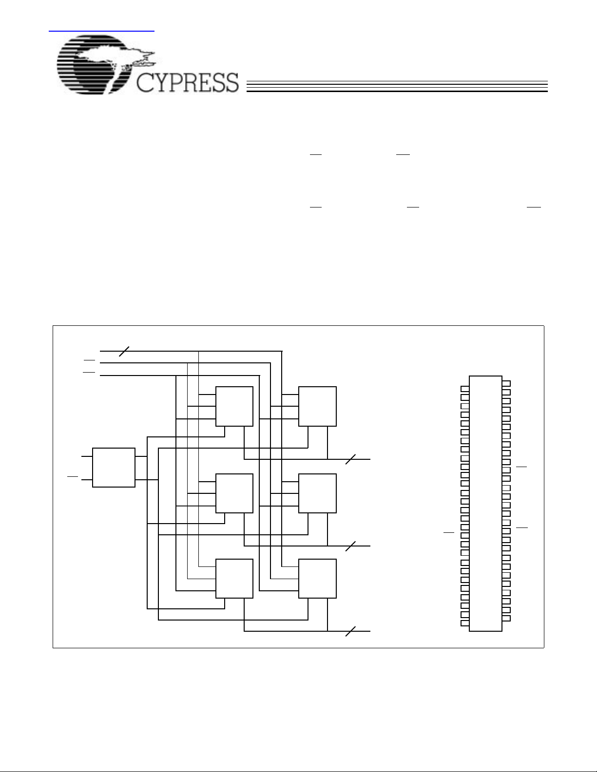
Functional Description
The CYM1730 is a high-performance 1.5M static RAM module
organized as 64K words by 24 bi ts. This module is c onstructed
Logic Block D iagram
A
0–A14
A
15
CS
OE
WE
DECODER
1 OF 2
15
32K x 8
SRAM
32K x 8
SRAM
32K x 8
SRAM
using six 32K x 8 static RAMs in SOJ packages mounted onto
an epoxy laminate board with pins.
Writing to the device is accomplished when the chip select
(CS
) and write enable (WE) inputs are both LOW. Data on the
input/output pins (I/O
into the memory location specified on the address pins (A
through I/O23) of the device is writ ten
0
through A15).
Reading the device is accomplished by taking the chip select
) and output enable (OE) LOW while write enable (WE)
(CS
remains HIGH. Under these conditions, the contents of the
memory location specified on the address pins will appear on
the input/output pins.
The input/output pins remain in a high-impedance state unle ss
the module is selected, outputs are enabled, and write enable
is HIGH.
Pin Configuration
ZIP
Top View
V
CC
1
2
4
6
8
10
12
14
16
18
20
22
24
26
28
30
32
34
36
38
40
42
44
46
48
50
52
54
56
I/O
I/O
I/O
I/O
GND
A
0
A
2
A
4
A
6
CS
NC
I/O
I/O
I/O
I/O
GND
WE
A
8
A
10
A
12
A
14
GND
I/O
I/O
I/O
I/O
V
CC
1730-2
0
2
4
6
8
10
12
14
16
18
20
22
3
5
7
9
11
13
15
17
19
21
23
25
27
29
31
33
35
37
39
41
43
45
47
49
51
53
55
32K x 8
SRAM
32K x 8
SRAM
32K x 8
SRAM
8
8
8
I/O16–I/O
I/O8–I/O
–I/O
I/O
0
1730-1
V
CC
I/O
1
I/O
3
I/O
5
I/O
7
GND
A
1
A
3
A
23
5
A
7
NC
GND
I/O
9
I/O
11
I/O
13
I/O
15
NC
OE
A
15
7
A
A
A
GND
I/O
I/O
I/O
I/O
V
CC
9
11
13
15
17
19
21
23
0
Cypress Semiconductor Corporation • 3901 North First Street • San Jose • CA 95134 • 408-943-2600
July 1991 – Revised January 1995
CYM1730
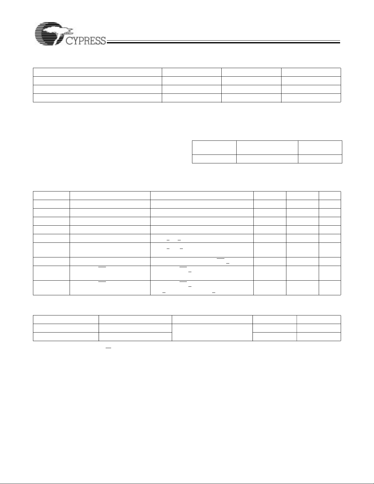
Selection G uide
1730–25 1730–30 1730–35
Maximum Access Time (ns) 25 30 35
Maximum Operati ng Current (mA) 510 510 510
Maximum Standby Current (mA) 180 180 180
Maximum Ratings
(Above which the useful life may be impaired. For user guide-
DC Input Voltage ................................. .......... –0.5V to +7.0V
lines, not tested.)
Storage Temperature .................................–55°C to +125°C
Ambient Temperature with
Power Applied...............................................–10°C to +85°C
Supply Voltage to Ground Potential............... –0.5V to +7.0V
Operating Range
Ambient
Range
Commercial 0°C to +70°C 5V ± 10%
Temperature
V
CC
DC Voltage Applied to Outputs
in High Z State ............................................... –0.5V to +7.0V
Electrical Characteristics Over the Operating Range
Parameter Description Test Conditions Min. Max. Unit
V
V
V
V
I
IX
I
OZ
I
CC
I
SB1
I
SB2
OH
OL
IH
IL
Output HIGH Voltage VCC = Min., IOH = –4.0 mA 2.4 V
Output LOW Voltage VCC = Min., IOL = 8.0 mA 0.4 V
Input HIGH Voltage 2.2 VCC + 0.3 V
Input LOW Voltage –0.3 0.8 V
Input Load Current GND < VI < V
CC
Output Leakage Current GND < VO < VCC,
–20 +20 µA
–10 +10 µA
Output Disabled
VCC Operating Supply Current VCC = Max., I
Automatic CS Power-Down
[1]
Current
Automatic CS Power-Down
[1]
Current
Max. VCC, CS > VIH,
Min. Duty Cycle = 100%
Max. VCC, CS > VCC – 0.2V,
V
> VCC – 0.2V or VIN < 0.2V
IN
= 0 mA, CS < V
OUT
IL
510 mA
180 mA
180 mA
Capacitance
[2]
Parameter Description Test Conditions Max. Unit
C
IN
C
OUT
Notes:
1. A pull-up resistor to V
2. Tested on a sample basis.
Input Capacitance TA = 25°C, f = 1 MHz,
V
= 5.0V
Output Capacitance 20 pF
on the CS input is required to keep the device deselected during VCC power-up, otherwise ISB will exceed values given.
CC
CC
50 pF
2

AC Test Loads and Waveforms
CYM1730
5V
OUTPUT
100 pF
INCLUDING
JIG AND
SCOPE
Equivalent to: THÉ VENIN EQUIVALENT
OUTPUT
481Ω 481Ω
255Ω 255Ω
(a) (b)
1730-5
167Ω
5V
OUTPUT
INCLUDING
JIG AND
SCOPE
1.73V
5 pF
Switching Characteristics Over the Operating Range
3.0V
GND
<5ns <5ns
1730-3 1730-4
[3]
ALL INPUT PULSES
90%
10%
90%
10%
1730–25 1730–30 1730–35
Parameter Descripti on Min. Max. Min. Max. Min. Max. Unit
READ CYCLE
t
RC
t
AA
t
OHA
t
ACS
t
DOE
t
LZOE
t
HZOE
t
LZCS
t
HZCS
WRITE CYCLE
t
WC
t
SCS
t
AW
t
HA
t
SA
t
PWE
t
SD
t
HD
t
LZWE
t
HZWE
Notes:
3. T est conditions assume signal transition time of 5 ns or less, timing reference levels of 1.5V, input pulse levels of 0 to 3.0V, and output loading of the specified
I
OL/IOH
4. At any given temperature and voltage condition, t
5. t
6. The internal write time of the memory is defined by the overlap of CS
, t
HZOE
terminate a write by going HIGH. The data input set-up and hold timing should be referenced to the rising edge of the signal that terminates the write.
Read Cycle Time 25 30 35 ns
Address to Data Valid 25 30 35 ns
Output Hold from Address Change 5 5 5 ns
CS LOW to Data Valid 25 30 35 ns
OE LOW to Data Valid 12 15 20 ns
OE LOW to Low Z 3 3 3 ns
OE HIGH to High Z 10 15 20 ns
CS LOW to Low Z
CS HIGH to High Z
[6]
Write Cycle Time 25 30 35 ns
CS LOW to Write End 20 25 30 ns
Address Set-Up to Write End 22 25 30 ns
Address Hold from Write End 2 2 2 ns
Address Set-Up to Write Start 2 2 2 ns
WE Pulse Width 20 23 25 ns
Data Set-Up to Write End 13 15 20 ns
Data Hold from Write End 2 2 2 ns
WE HIGH to Low Z 3 3 5 ns
WE LOW to High Z
and 30-pF load capacitance.
HZCS
, and t
are specified with CL = 5 pF as in part (b) of AC Test Loads and Waveforms. Transition is measured ±500 mV from steady-state voltage.
LZCE
[4]
[4, 5]
[5]
is less than t
HZCS
5 5 5 ns
10 15 15 ns
0 10 0 10 0 15 ns
for any given device.
LZCS
LOW and WE LOW. Both signals must be LOW to initiate a write and either signal can
3

Switching Waveforms
CYM1730
ReadCycleNo. 1
ADDRESS
DATA OUT
ReadCycleNo. 2
CS
OE
DATA OUT
V
CC
SUPPLY
CURRENT
[7, 8]
t
RC
t
t
OHA
AA
PREVIOUS DATA VALID DATA VALID
[7, 9]
t
RC
t
ACS
t
DOE
t
LZOE
HIGH IMPEDANCE
t
LZCS
t
PU
DATA VALID
50%
t
HZOE
t
HZCS
t
PD
1730-6
HIGH
IMPEDANCE
ICC
50%
ISB
1730-7
Write Cycle No. 1 (WE Controlled)
[6, 10]
ADDRESS
CS
t
SA
WE
DATA IN
OUT
DATA
Notes:
7. WE
is HIGH for read cycle.
8. Device is continuously selected, CS = VIL and OE= VIL.
9. Address valid prior to or coincident with CS
10. Data I/O will be high impedance if OE = VIH.
DATA UNDEFINED
transition LOW.
t
SCS
t
AW
t
WC
DATA VALID
t
HZWE
t
PWE
t
HA
t
SD
t
HD
t
LZWE
HIGH IMPEDANCE
1730-8
4

Switching Waveforms (continued)
CYM1730
WriteCycleNo.2 (CS Controlled)
ADDRESS
CS
WE
DATA IN
DATA OUT
Note:
11. If CS
goes HIGH simultaneously with WE HIGH, the output remains in a high-impedance state.
[6, 10, 11]
t
SA
DATA UNDEFINED
Trut h Table
CS WE OE Input/Outputs Mode
H X X High Z Deselect/Power-Down
L H L Data Out Read Word
L L X Data In Write Word
L H H High Z Deselect
t
AW
t
WC
t
SCS
t
PWE
t
SD
DATA VALID
t
HZWE
t
HA
t
HD
HIGH IMPEDANCE
1730-9
Ordering Info rma tio n
Speed
(ns)
Ordering Code
25 CYM1730PZ–25C PZ07 56-Pin ZI P Module Commercial
30 CYM1730PZ–30C PZ07 56-Pin ZI P Module Commercial
35 CYM1730PZ–35C PZ07 56-Pin ZI P Module Commercial
Document #: 38–M–00049–A
Package
Name
Package Type
Operating
Range
5

Package Diagram
CYM1730
56-Pi n ZIP Module PZ07
2.990/3.010
2.750 R EF
.350 MAX.
.485/.495
.125/.175
.100 REF
© Cypress Semiconductor Corporation, 1995. The information contained herein is subject to change without notice. Cypress Semiconductor Corporation assumes no responsibility for the use
of any circ uitry other than circui try embodi ed in a Cypress Semi conductor p roduct. Nor does it convey or imply any li cense under patent or other rights . Cypress Semi conductor does not authori ze
its products for use as critical components in life-support systems where a malfunction or failure may reasonably be expected to result in significant injury to the user. The inclusion of Cypress
Semiconductor products in life-support systems application implies that the manufacturer assumes all risk of such use and in doing so indemnifies Cypress Semiconductor against all charges.
 Loading...