

512K x 8 SRAM Module
CYM1465
1CYM146 5
查询CYM1465供应商
Features
• High-density 4-megabit SRAM module
• High-speed CMOS SRAMs
—Access time of 70 ns
• Low active power
—605 mW (max.)
• 2V data retention (L Version)
• JEDEC-compatible pinout
• 32-pin, 0.6-inch-wide DIP package
• TTL-compatible inputs and outputs
• Low profile
—Max. height of 0.27 in.
• Small PCB footprint
—0.98 sq. in.
Functional Description
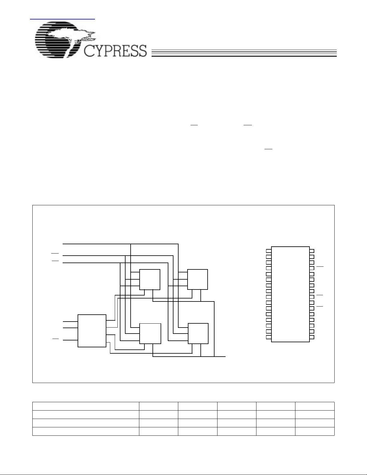
The CYM1465 is a high-performance 4-megabit static RAM
module organized as 512K words by 8 bits. This module is
constructed using four 128K x 8 RAMs mounted on a substrate
with pins. A decoder is used to interpret the higher-order addresses (A
Writing to the module is accomplished when the chip select
) and write enable (WE) inputs are both LOW. Data on the
(CS
eight input/output pins (I/O
ten into the memory location specified o n the a ddress pins (A
through A18). Reading the device is accomplished by taking
chip select and output enable (OE
remains inactive or HIGH. Under these conditions, the contents of the memory location spec i fied o n the address pins (A
through A18) will appear on the eight appropriate data input/output pins (I/ O
The input/output pins remain in a high-impedance state unle ss
and A18) and to select one of the four RAMs.
17
through I/O7) of the device is writ-
0
) LOW while write enable
through I/O7).
0
the module is selected, outputs are enabled, and write enable
is HIGH.
Logic Block Diagram Pin Configuration
DIP
0
1
2
Top View
1
S
2
3
4
5
6
7
8
9
10
11
12
13
14
15
16
A0− A
16
WE
OE
A
A
CS
A
18
A
16
A
14
A
12
A
128K x 8
SRAM
17
18
1 OF 4
DECODER
128K x 8
SRAM
128K x 8
SRAM
128K x 8
SRAM
A
A
A
A
A
A
A
I/O
I/O
I/O
GND
7
6
5
4
3
2
1
0
0
0
32
V
CC
31
A
15
A
30
17
29
WE
28
A
13
27
A
8
26
A
9
A
25
11
24
OE
A
23
10
22
CS
21
I/O
I/O
I/O
I/O
I/O
7
6
5
4
3
20
19
18
17
1465–2
1465–1
I/O − I/O
0
7
Selection G uide
1465-70 1465-85 1465-100 1465-120 1465-150
Maximum Access Time (ns) 70 85 100 120 150
Maximum Operati ng Current (mA) 110 110 110 110 110
Maximum Standby Current (mA) 12 12 12 12 12
Cypress Semiconductor Corporation • 3901 North First Street • San Jose • CA 95134 • 408-943-2600
January 1991 – Revised January 1995
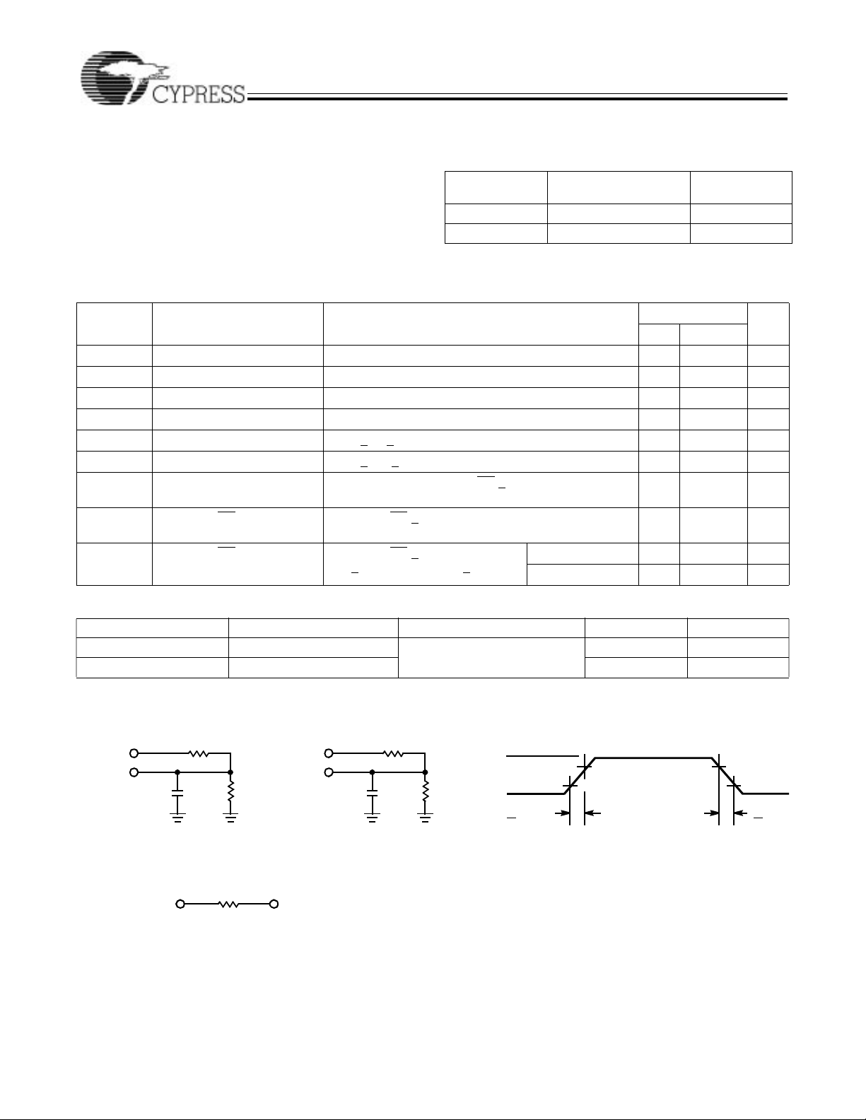
(a)
(b)
1465–3 1465–4
5V
90%
10%
3.0V
GND
90%
10%
OUTPUT
INCLUDING
JIG AND
SCOPE
5V
OUTPUT
5 pF
INCLUDING
JIG AND
SCOPE
ALL INPUT PULSES
<10ns
1.847k Ω 1.847k
Ω
OUTPUT
C
L
[2]
1kΩ1kΩ
Equiva le nt to: THÉ VENIN EQUIVALENT
<10ns
648Ω
1.76V
CYM1465
Maximum Ratings
(Above which the useful life may be impaired.)
Storage Temperature . ................................–55°C to +150°C
Ambient Temperature with
Power Applied...............................................–10°C to +85°C
Supply Voltage to Ground Potential...............–0.5V to +7.0V
DC Input Voltage ................................. ............-0.5V to +7.0V
Operating Range
Ambient
Range
Commercial 0°C to +70°C 5V ± 10%
Industrial –40°C to +85°C 5V ± 10%
Temperature
V
CC
DC Voltage Applied to Outputs
in High Z State ............................................... –0.5V to +7.0V
Electrical Characteristics Over the Operating Range
1465
Parameter Description Test Conditions Min. Max. Unit
V
OH
V
OL
V
IH
V
IL
I
IX
I
OZ
I
CC
I
SB1
I
SB2
Capacitance
C
IN
C
OUT
Output HIGH Voltage VCC = Min., IOH = –1.0 mA 2.4 V
Output LOW Voltage VCC = Min., IOL = 2.1 mA 0.4 V
Input HIGH Voltage 2.2 VCC + 0.3 V
Input LOW Voltage –0.3 0.8 V
Input Load Current GND < VI < V
CC
–10 +10 µA
Output Leakage Current GND < VO < VCC, Output Disabled –20 +20 µA
VCC Operating Supply
Current
Automatic CS Power-Down
Current
Automatic CS Power-Down
Current
[1]
VCC = Max., I
= 0 mA, CS < V
OUT
Max. VCC, CS > VIH,
Min. Duty Cycle = 100%
Max. VCC, CS > VCC - 0.2V,
V
> VCC - 0.2V or VIN < 0.2V
IN
IL
110 mA
12 mA
Standard Version 8 mA
L Version 420 µA
Parameter Description Test Conditions Max. Unit
Input Capacitance TA = 25°C, f = 1 MHz,
V
= 5.0V
Output Capacitance 45 pF
CC
45 pF
AC Test Loads and Waveforms
Notes:
1. Tested on a sample basis.
2

1465–5
4.5V4.5V
CS
V
CC
t
CDR
VDR> 2V
DATA RETENTION MODE
V
DR
t
R
V
IH
V
IH
CYM1465
Switching Characteristics Over the Operating Range
[2]
1465-70 1465-85 1465-100 1465-120 1465-150
Parameter Description Mi n. Max. Min. Max. Min. Max. Min. Max. Min. Max. Unit
READ CYCLE
t
RC
t
AA
t
OHA
t
ACS
t
DOE
t
LZOE
t
HZOE
t
LZCS
t
HZCS
WRITE CYCLE
t
WC
t
SCS
t
AW
t
HA
t
SA
t
PWE
t
SD
t
HD
t
LZWE
t
HZWE
Read Cycle Time 70 85 100 120 150 ns
Address to Data Valid 70 85 100 120 150 ns
Data Hold from Address Change 10 10 10 10 10 ns
CS LOW to Data Valid 70 85 100 120 150 ns
OE LOW to Data Valid 35 45 50 60 75 ns
OE LOW to Low Z 5 5 5 5 5 ns
OE HIGH to High Z
[3]
25 30 35 45 55 ns
CS LOW to Low Z 10 10 10 10 10 ns
CS HIGH to High Z
[4]
[3]
30 30 35 45 60 ns
Write Cycle Time 70 85 100 120 150 ns
CS LOW to Write End 65 75 90 100 115 ns
Address Set-Up to Write End 65 75 90 100 110 ns
Address Hold from Write End 0 5 5 5 5 ns
Address Set-Up to Write Start 0 5 5 5 5 ns
WE Pulse Width 55 65 75 85 95 ns
Data Set-Up to Write End 30 35 40 45 50 ns
Data Hold from Write End 0 0 0 0 0 ns
WE HIGH to Low Z 5 5 5 5 5 ns
WE LOW to High Z
[3]
25 30 35 40 45 ns
Data Retention Characteristics Over the Operating Range (L Version Only)
Commercial Industrial
Parameter Description Test Conditions Min. Max. Min. Max. Unit
V
DR
I
CCDR3
[5]
t
CDR
[5]
t
R
Notes:
2. Test conditions assume signal transition times of 10 ns or less, timing reference levels of 1.5V, input levels of 0 to 3.0V, and output loading of the specified
I
OL/IOH
3. CL = 5 pF as in part (b) of AC Test Loads and Waveforms. Transition is measured ±500 mV from steady-state voltage.
4. The internal write time of the memory is defined by the overlap of CS
terminate a write by going HIGH. The data input set-up and hold timing should be referenced to the rising edge of the signal that terminates the write.
5. Guaranteed, not tested.
VCC for Retention Data CS > VCC – 0.2V 2 2 V
Data Retention Current VDR = 3.0V,
CS
Chip Deselect to Data Retention Time 0 0 ns
Operation Recovery Time 5 5 ms
and 100-pF load capacitance for 85-, 100-, 120-, and 150-ns speeds. CL = 30 pF for 70-ns speed.
> VCC – 0.2V,
V
> VCC – 0.2V or
IN
V
< 0.2V
IN
LOW and WE LOW. Both signals must be LOW to initiate a write and either signal can
50 150 µA
Data Retention Waveform
3

Switching Waveforms
CYM1465
Read Cycle No. 1
ADDRESS
DATA OUT
Read Cycle No. 2
CS
OE
DATA OUT
[6,7]
t
RC
t
t
OHA
AA
PREVIOUS DATA VALID DATA VALID
[6,8]
t
RC
t
ACS
t
DOE
t
LZOE
HIGH IMPEDANCE
t
LZCS
DATA VALID
t
HZOE
t
HZCS
1465–6
HIGH
IMPEDANCE
1465–7
Write Cycle No. 1
(WE
Controlled)
ADDRESS
CS
WE
DATA IN
DATA
OUT
Notes:
6. WE
is HIGH for read cycle.
7. Device is co ntinuously selected, CS = VIL.
8. Address valid prior to or coincident with CS
[4]
t
SA
DATA UNDEFINED
transition LOW.
t
SCS
t
AW
t
WC
t
HZWE
t
PWE
t
SD
DATA VALID
t
HA
t
HD
t
LZWE
HIGH IMPEDANCE
1465–8
4

Switching Waveforms (continued)
CYM1465
Write Cycle No. 2 (CS Controlled)
[4,9]
ADDRESS
t
SA
CS
WE
DATA IN
DATA
Note:
9. If CS
OUT
goes HIGH simultaneously with WE HIGH, the output remains in a high-impedance state.
DATA UNDEFINED
Trut h Table
Inputs
CS WE OE Output Mode
H X X High Z Deselect/Power-Down
L H L Data Out Read Word
L L X Data In Write Word
L H H High Z Deselect
t
AW
t
WC
t
SCS
t
PWE
t
SD
DATA VALID
t
HZWE
t
HA
t
HD
HIGH IMPEDANCE
1465–9
5

Ordering Info rma tio n
CYM1465
Speed
(ns) Ordering Code
70 CYM1465PD-70C PD03 32-Pin DIP Module Commercial
CYM1465LPD-70C
85 CYM1465PD-85C PD03 32-Pin DIP Module Commercial
CYM1465LPD-85C
CYM1465PD-85I PD03 32-Pin DIP Module Industrial
CYM1465LPD-85I
100 CYM1465PD-100C PD03 32-Pin DIP Module Commercial
CYM1465LPD-100C
CYM1465PD-100I PD03 32-Pin DIP Module Industrial
CYM1465LPD-100I
120 CYM1465PD-120C PD03 32-Pin DIP Module Commercial
CYM1465LPD-120C
CYM1465PD-120I PD03 32-Pin DIP Module Industrial
CYM1465LPD-120I
150 CYM1465PD-150C PD03 32-Pin DIP Module Commercial
CYM1465LPD-150C
CYM1465PD-150I PD03 32-Pin DIP Module Industrial
CYM1465LPD-150I
Document #: 38-M-00036-D
Package
Name Package Type
Operating
Range
Package Diagrams
32–Pin DIP Module PD03
© Cypress Semiconductor Corporation, 1995. The information contained herein is subject to change without notice. Cypress Semiconductor Corporation assumes no responsibility for the use
of any circ uitry other than circui try embodi ed in a Cypress Semi conductor p roduct. Nor does it convey or imply any li cense under patent or other rights . Cypress Semi conductor does not authori ze
its products for use as critical components in life-support systems where a malfunction or failure may reasonably be expected to result in significant injury to the user. The inclusion of Cypress
Semiconductor products in life-support systems application implies that the manufacturer assumes all risk of such use and in doing so indemnifies Cypress Semiconductor against all charges.
 Loading...