

Page 1
CYD01S36V
CYD02S36V/36VA/CYD04S36V
CYD09S36V/CYD18S36V
FLEx36™ 3.3V 32K/64K/128K/256K/512 x 36
Synchronous Dual-Port RAM
Features
Functional Description
■ True dual-ported memory cells that enable simultaneous
access of the same memory location
■ Synchronous pipelined operation
■ Family of 1-Mbit, 2-Mbit, 4-Mbit, 9-Mbit and 18-Mbit devices
■ Pipelined output mode allows fast operation
■ 0.18 micron CMOS for optimum speed and power
■ High speed clock to data access
■ 3.3V low power
❐ Active as low as 225 mA (typ.)
❐ Standby as low as 55 mA (typ.)
■ Mailbox function for message passing
■ Global master reset
■ Separate byte enables on both ports
■ Commercial and industrial temperature ranges
■ IEEE 1149.1-compatible JTAG boundary scan
■ 256 Ball FBGA (1-mm pitch)
■ Counter wrap around control
❐ Internal mask register controls counter wrap-around
❐ Counter-interrupt flags to indicate wrap-around
❐ Memory block retransmit operation
■ Counter readback on address lines
■ Mask register readback on address lines
■ Dual Chip Enables on both ports for easy depth expansion
■ Seamless migration to next-generation dual-port family
The FLEx36™ family includes 1-Mbit, 2-Mbit, 4-Mbit, 9-Mbit, and
18-Mbit pipelined, synchronous, true dual-port static RAMs that
are high speed, low power 3.3V CMOS. Two ports are provided,
permitting independent, simultaneous access to any location in
memory. A particular port can write to a certain location while
another port is reading that location. The result of writing to the
same location by more than one port at the same time is
undefined. Registers on control, address, and data lines allow for
minimal setup and hold time.
During a Read operation, data is registered for decreased cycle
time. Each port contains a burst counter on the input address
register. After externally loading the counter with the initial
address, the counter increments the address internally (more
details to follow). The internal Write pulse width is independent
of the duration of the R/W
input signal. The internal Write pulse
is self-timed to allow the shortest possible cycle times.
A HIGH on CE0
or LOW on CE1 for one clock cycle powers down
the internal circuitry to reduce the static power consumption. One
cycle with chip enables asserted is required to reactivate the
outputs.
Additional features include: readback of burst-counter internal
address value on address lines, counter-mask registers to
control the counter wrap-around, counter interrupt (CNTINT
flags, readback of mask register value on address lines,
retransmit functionality, interrupt flags for message passing,
JTAG for boundary scan, and asynchronous Master Reset
(MRST
).
The CYD18S36V devices in this family has limited features.
Please see Address Counter and Mask Register Operations
on page 5 for details.
Seamless Migration to Next-Generation Dual-Port
Family
Cypress offers a migration path for all devices in this family to the
next-generation devices in the Dual-Port family with a compatible
footprint. Please contact Cypress Sales for more details.
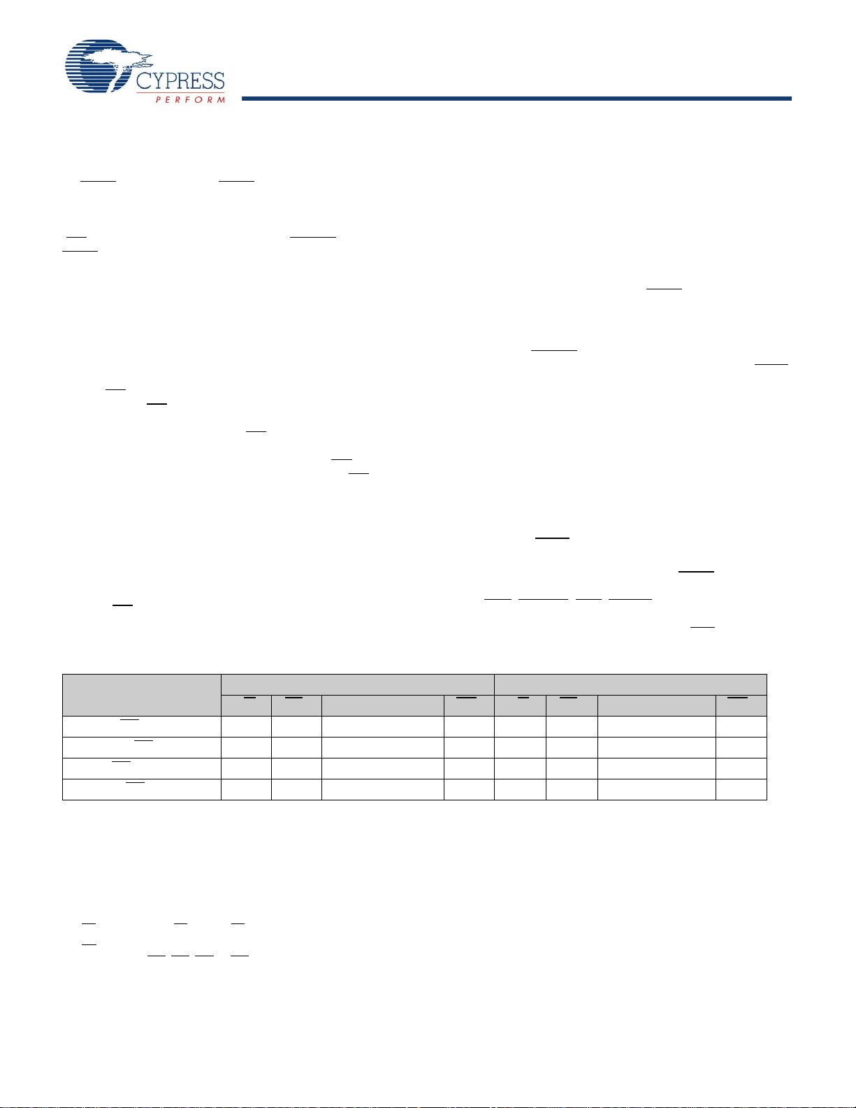
Table 1. Product Selection Guide
Density
1 Mbit
(32K x 36)
2 Mbit
(64K x 36)
4 Mbit
(128K x 36)
9 Mbit
(256K x 36)
18 Mbit
(512K x 36)
Part Number CYD01S36V CYD02S36V/36VA CYD04S36V CYD09S36V CYD18S36V
Max. Speed (MHz) 167 167 167 167 133
Max. Access Time – Clock to Data
4.0 4.4 4.0 4.0 5.0
(ns)
Typical Operating Current (mA) 225 225 225 270 315
Package 256 FBGA
(17 mm x 17 mm)
256 FBGA
(17 mm x 17 mm)
256 FBGA
(17 mm x 17 mm)
256 FBGA
(17 mm x 17 mm)
256 FBGA
(23 mm x 23 mm)
)
[19]
Cypress Semiconductor Corporation • 198 Champion Court • San Jose, CA 95134-1709 • 408-943-2600
Document Number: 38-06076 Rev. *G Revised Decenber 09, 2008
[+] Feedback
Page 2
CYD01S36V
CYD02S36V/36VA/CYD04S36V
CYD09S36V/CYD18S36V
Logic Block Diagram
FTSEL
L
PORTSTD[1:0]
L
DQ [35:0]
L
BE [3:0]
L
CE0
L
CE1
L
OE
L
R/W
L
FTSEL
R
PORTSTD[1:0]
R
DQ [35:0]
R
BE [3:0]
R
CE0
R
CE1
R
OE
R
R/W
R
A [18:0]
L
CNT/MSK
L
ADS
L
CNTEN
L
CNTRST
L
RET
L
CNTINT
L
C
L
WRP
L
A [18:0]
R
CNT/MSK
R
ADS
R
CNTEN
R
CNTRST
R
RET
R
CNTINT
R
C
R
WRP
R
CONFIG Block CONFIG Block
IO
Control
IO
Control
Dual Ported Array
Address &
Counter Logic
Address &
Counter Logic
INT
L
TRST
TMS
TDI
TDO
TCK
JTAG
MRST
READY
R
LowSPD
R
READY
L
LowSPD
L
RESET
LOGIC
INT
R
BUSY
L
BUSY
R
Mailboxes
Arbitration Logic
Note
1. 18-Mbit device has 19 address bits, 9-Mbit device has 18 address bits, 4-Mbit device has 17 address bits, 2-Mbit device has 16 address bits, and 1-Mbit device has
15 address bits.
[1]
Document Number: 38-06076 Rev. *G Page 2 of 28
[+] Feedback
Page 3
CYD01S36V
CYD02S36V/36VA/CYD04S36V
CYD09S36V/CYD18S36V
Pin Configurations
Figure 1. Pin Diagram - 256-Ball FBGA (Top View)
CYD01S36V/CYD02S36V/36VA/CYD04S36V/CYD09S36V/CYD18S36V
1 2 3 4 5 6 7 8 9 10 11 12 13 14 15 16
DQ32L DQ30L DQ28L DQ26L DQ24L DQ22L DQ20L DQ18L DQ18R DQ20R DQ22R DQ24R DQ26R DQ28R DQ30R DQ32R
A
DQ33L DQ31L DQ29L DQ27L DQ25L DQ23L DQ21L DQ19L DQ19R DQ21R DQ23R DQ25R DQ27R DQ29R DQ31R DQ33R
B
L
A15L
[6]
A17L
[8]
A19L
[2,5]
RET
WRP
CE0
CNTINT
L [12]
BUSY
ADSL
R/WL
CNT/M
SKL [10]
CNTEN
L [11]
DQ34L DQ35L
C
A0L A1L
D
A2L A3L
E
A4L A5L
F
A6L A7L
G
A8L A9L CL VTTL VCORE VSS VSS VSS VSS VSS VSS VCORE VTTL CR A9R A8R
H
A10L A11L VSS
J
A12L A13L OELBE1L VDDIOL VSS VSS VSS VSS VSS VSS
K
A14L
L
A16L
M
[7]
A18L
N
[9]
DQ16L DQ17L
P
INT
[2,3]
L
VREFL
[2,3]
[2,5]
[2,4]
L
CE1L
[11]
[11]
[10]
BE3
L
BE2
PORTS
TD1L[2,4]VCORE VSS VSS VSS VSS VSS VSS VCORE
BE0L VDDIOL VSS VSS VSS VSS VSS VSS
REVL
[2,4]
VREFL
[2,4]
CNTRS
TL [10]
N C
L
[2,5]
FTSELL
[2,3]
VDDIOL VDDIOL VDDIOL VCORE VCORE
L VDDIOL VSS VSS VSS VSS VSS VSS
REV
L
[2,3]
VDDIOL VDDIOL VDDIOL VCORE VCORE
PortST
D0L
[2,4]
N C
[2,5]
N C
REVL
[2,5]
LOWSP
DL [2,4]
L
VSS VSS VSS VSS VSS VSS
READY
L [2,5]
[2,5]
[2,4]
VSS VTTL VTTL VSS
REV
L
[2,3]
N C
TCK TMS TDO TDI
TRST
MRST
[2,5]
VTTL VTTL
NC
[2,5]
VDDIORVDDIORVDDIORCE1R
VDDIORVDDIORVDDIORREVR
REV
[2,3]
R
N C
[2,5]
LOWSP
DR [2,4]
READY
R [2,5]
N C
[2,5]
N C
[2,5]
FTSEL
R [ 2, 3]
VDDIO
R
VDDIO
R
VDDIO
R
VDDIO
R
PortST
D0R
[2,4]
N C
[2,5]
INT
R
VREFL
[2,4]
[10]
BE3R
BE2R
PORTS
TD1R[2,4]VSS A11R A10R
BE1ROER A13R A12R
BE0R
[2,4]
VREFR
[2,4]
CNTRS
TR [10]
R
RET
[2,3]
WRP
[2,3]
CE0R
[11]
CNTINT
R [12]
BUSY
[2,5]
ADSR
[11]
R/WR
CNT/M
SKR
[10]
CNTEN
R [11]
DQ35R DQ34R
R
R
DQ17R DQ16R
A1R A0R
A3R A2R
A5R A4R
A7R A6R
A15R
A14R
[6]
A17R
A16R
[8]
A19R
A18R
[2,5]
[7]
[9]
DQ15L DQ13L DQ11L DQ9L DQ7L DQ5L DQ3L DQ1L DQ1R DQ3R DQ5R DQ7R DQ9R DQ11R DQ13R DQ15R
R
DQ14L DQ12L DQ10L DQ8L DQ6L DQ4L DQ2L DQ0L DQ0R DQ2R DQ4R DQ6R DQ8R DQ10R DQ12R DQ14R
T
Notes
2. This ball represents a next generation Dual-Port feature. For more information about this feature, contact Cypress Sales.
3. Connect this ball to VDDIO. For more information about this next generation Dual-Port feature contact Cypress Sales.
4. Connect this ball to VSS. For more information about this next generation Dual-Port feature, contact Cypress Sales.
5. Leave this ball unconnected. For more information about this feature, contact Cypress Sales.
6. Leave this ball unconnected for 32K x 36configuration.
7. Leave this ball unconnected for a 64K x 36, 32K x 36 configurations.
8. Leave this ball unconnected for a 128K x 36, 64K x 36 and 32K x 36 configurations.
9. Leave this ball unconnected for a 256K x 36, 128K x 36, 64K x 36, and 32K x 36 configurations.
10. These balls are not applicable for CYD18S36V device. They need to be tied to VDDIO.
11. These balls are not applicable for CYD18S36V device. They need to be tied to VSS.
12. These balls are not applicable for CYD18S36V device. They need to be no connected.
Document Number: 38-06076 Rev. *G Page 3 of 28
[+] Feedback
Page 4
CYD01S36V
CYD02S36V/36VA/CYD04S36V
CYD09S36V/CYD18S36V
Pin Definitions
Left Port Right Port Description
A
0L–A18L
BE
–BE
0L
[2,5]
BUSY
L
C
L
[11]
CE0
L
[10]
CE1
L
DQ
–DQ
0L
OE
L
INT
L
LowSPD
L
[2,4]
PORTSTD[1:0]
R/W
L
ADS
RET
V
DDIOL
L
L
[2,3]
L
L
[2, 3, 4]
L
L
[11]
L
L
L
[2,3]
[2,3]
L
[2,4]
[2,5]
L
[11]
[12]
READY
CNT/MSK
CNTEN
CNTRST
CNTINT
WRP
FTSEL
VREF
REV
3L
35L
[2,4]
L
[10]
[10]
MRST
TRST
TMS JTAG Test Mode Select Input. It controls the advance of JTAG TAP state machine. State
TCK JTAG Test Clock Input.
TDO JTAG Test Data Output. TDO transitions occur on the falling edge of TCK. TDO is
V
V
CORE
V
A0R–A
BE0R–BE
BUSY
R
C
R
CE0
R
[10]
CE1
R
DQ0R–DQ
OE
R
INT
R
18R
3R
[2,5]
[11]
35R
Address Inputs.
Byte Enable Inputs. Asserting these signals enables Read and Write operations to the
corresponding bytes of the memory array.
Port Busy Output. When the collision is detected, a BUSY is asserted.
Input Clock Signal.
Active Low Chip Enable Input.
Active High Chip Enable Input.
Data Bus Input/Output.
Output Enable Input. This asynchronous signal must be asserted LOW to enable the DQ
data pins during Read operations.
Mailbox Interrupt Flag Output. The mailbox permits communications between ports. The
upper two memory locations can be used for message passing. INT
when the right port writes to the mailbox location of the left port, and vice versa. An interrupt
to a port is deasserted HIGH when it reads the contents of its mailbox.
R/W
V
DDIOR
R
R
[2,3]
R
R
R
[2, 3, 4]
R
R
R
R
[11]
R
R
R
[2,3]
[2,3]
[2,4]
[2,4]
[2,5]
[10]
R
[11]
[10]
[12]
Port Low Speed Select Input.
[2,4]
Port Address/Control/Data IO Standard Select Inputs.
R
Read/Write Enable Input. Assert this pin LOW to write to, or HIGH to Read from the dual
port memory array.
Port Ready Output. This signal is asserted when a port is ready for normal operation.
Port Counter/Mask Select Input. Counter control input.
Port Counter Address Load Strobe Input. Counter control input.
Port Counter Enable Input. Counter control input.
Port Counter Reset Input. Counter control input.
Port Counter Interrupt Output. This pin is asserted LOW when the unmasked portion of
the counter is incremented to all “1s”.
Port Counter Wrap Input. The burst counter wrap control input.
Port Counter Retransmit Input. Counter control input.
Flow-Through Select. Use this pin to select Flow-Through mode. When is de-asserted,
the device is in pipelined mode.
Port External High-Speed IO Reference Input.
Port IO Power Supply.
Reserved pins for future features.
LowSPD
PORTSTD[1:0]
READY
CNT/MSK
ADS
CNTEN
CNTRST
CNTINT
WRP
RET
FTSEL
VREF
REV
Master Reset Input. MRST is an asynchronous input signal and affects both ports. A
maser reset operation is required at power up.
[2,5]
JTAG Reset Input.
machine transitions occur on the rising edge of TCK.
TDI JTAG Test Data Input. Data on the TDI input is shifted serially into selected registers.
normally three-stated except when captured data is shifted out of the JTAG TAP.
SS
[13]
TTL
Ground Inputs.
Core Power Supply.
LVTTL Power Supply for JTAG IOs
is asserted LOW
L
Document Number: 38-06076 Rev. *G Page 4 of 28
[+] Feedback
Page 5
CYD01S36V
CYD02S36V/36VA/CYD04S36V
CYD09S36V/CYD18S36V
Master Reset
The FLEx36 family devices undergo a complete reset by taking
its MRST
nously to the clocks. An MRST initializes the internal burst
counters to zero, and the counter mask registers to all ones
(completely unmasked). MRST also forces the Mailbox Interrupt
(INT
MRST
power up.
input LOW. The MRST input can switch asynchro-
) flags and the Counter Interrupt (CNTINT) flags HIGH.
must be performed on the FLEx36 family devices after
Mailbox Interrupts
The upper two memory locations may be used for message
passing and permit communications between ports. Ta b le 2
shows the interrupt operation for both ports of CYD18S36V. The
highest memory location, 7FFFF is the mailbox for the right port
and 7FFFE is the mailbox for the left port. Table 2 shows that to
set the INT
7FFFF asserts INT
Write to generate an interrupt. A valid Read of the 7FFFF
location by the right port resets INTR HIGH. At least one byte
must be active in order for a Read to reset the interrupt. When
one port Writes to the other port’s mailbox, the INT of the port
that the mailbox belongs to is asserted LOW. The INT
when the owner (port) of the mailbox Reads the contents of the
mailbox. The interrupt flag is set in a flow-thru mode (i.e., it
follows the clock edge of the writing port). Also, the flag is reset
in a flow-thru mode (i.e., it follows the clock edge of the reading
port).
Each port can read the other port’s mailbox without resetting the
interrupt. And each port can write to its own mailbox without
setting the interrupt. If an application does not require message
passing, INT
Table 2. Interrupt Operation Example
flag, a Write operation by the left port to address
R
LOW. At least one byte must be active for a
R
is reset
pins must be left open.
[1, 14, 15, 16, 17, 18]
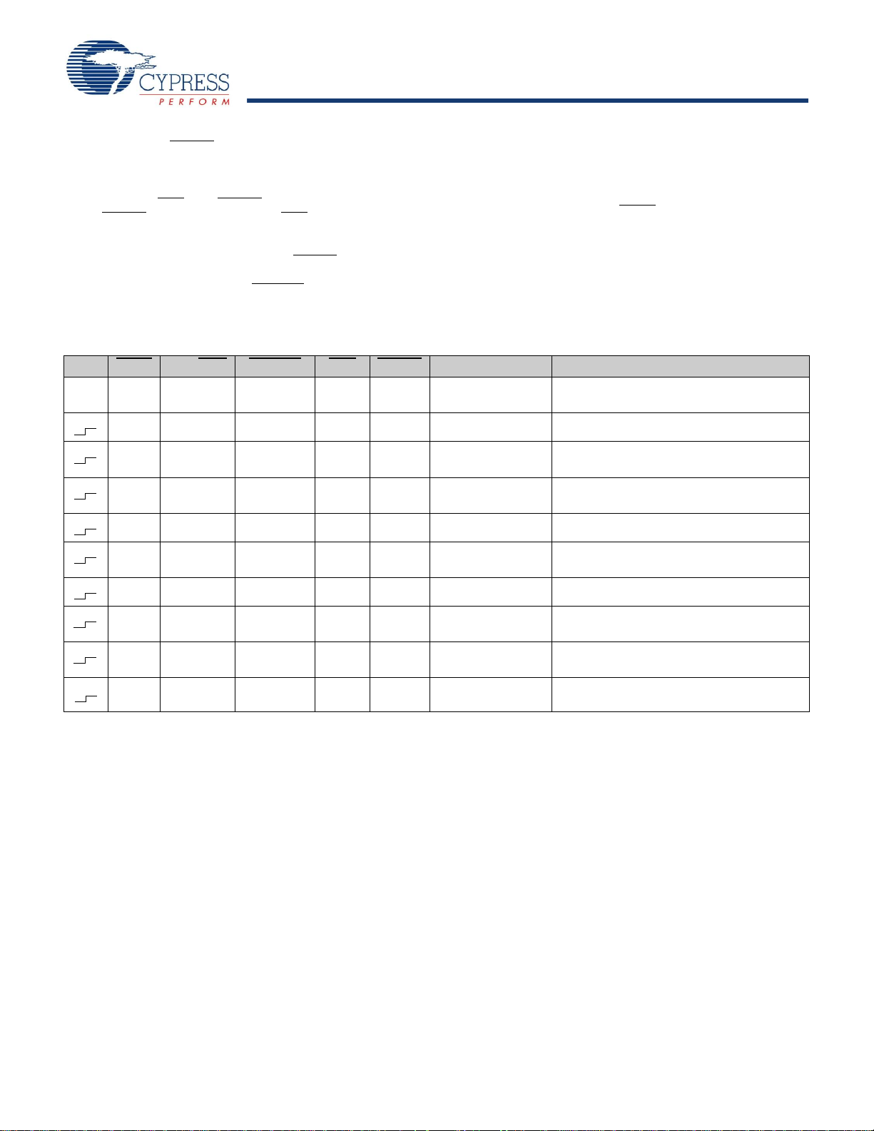
Address Counter and Mask Register
Operations
This section describes the features only apply to 1Mbit, 2 Mbit,
4 Mbit and 9 Mbit devices. It does not apply to 18Mbit device.
Each port of these devices has a programmable burst address
counter. The burst counter contains three registers: a counter
register, a mask register, and a mirror register.
The counter register contains the address used to access the
RAM array. It is changed only by the Counter Load, Increment,
Counter Reset, and by master reset (MRST
The mask register value affects the Increment and Counter
Reset operations by preventing the corresponding bits of the
counter register from changing. It also affects the counter
interrupt output (CNTINT
the Mask Load and Mask Reset operations, and by the MRST
The mask register defines the counting range of the counter
register. It divides the counter register into two regions: zero or
more “0s” in the most significant bits define the masked region,
one or more “1s” in the least significant bits define the unmasked
region. Bit 0 may also be “0,” masking the least significant
counter bit and causing the counter to increment by two instead
of one.l
The mirror register is used to reload the counter register on
increment operations (see “retransmit,” below). It always
contains the value last loaded into the counter register, and is
changed only by the Counter Load, and Counter Reset operations, and by the MRST
Table 3 on page 6 summarizes the operation of these registers
and the required input control signals. The MRST
is asynchronous. All the other control signals in Ta b l e 3 on page
6 (CNT/MSK, CNTRST, ADS, CNTEN) are synchronized to the
port’s CLK. All these counter and mask operations are
independent of the port’s chip enable inputs (CE0 and CE1).
[19]
) operations.
). The mask register is changed only by
.
control signal
.
Function
R/W
CE
L
Left Port Right Port
L
A
0L–18L
INT
R/W
L
CE
R
R
A
0R–18R
INT
R
Set Right INTR Flag L L 7FFFF X X X X L
Reset Right INT
Set Left INT
Reset Left INT
Notes
13. This family of Dual-Ports does not use V
Please contact local Cypress FAE for more information.
is internal signal. CE = LOW if CE0 = LOW and CE1 = HIGH. For a single Read operation, CE only needs to be asserted once at the rising edge of the CLK and
14. CE
can be deasserted after that. Data is out after the following CLK edge and is three-stated after the next CLK edge.
is “Don’t Care” for mailbox operation.
15. OE
16. At least one of BE0
17. A17x is a NC for CYD04S36V, therefore the Interrupt Addresses are 1FFFF and 1FFFE. A17x and A16x are NC for CYD02S36V/36VA, therefore the Interrupt Addresses
are FFFF and FFFE; A17x, A16x and A15x are NC for CYD01S36V, therefore the Interrupt Addresses are 7FFF and 7FFE.
18. “X” = “Don’t Care,” “H” = HIGH, “L” = LOW.
19. This section describes the CYD09S36V, CYD04S36V, CYD02S36V/36VA, and CYD01S36V which have 18, 17, 16 and 15 address bits.
Document Number: 38-06076 Rev. *G Page 5 of 28
FlagXXXXHL7FFFFH
R
Flag X X X L L L 7FFF E X
L
Flag H L 7FFFE H X X X X
L
, and these pins are internally NC. The next generation Dual-Port family, the FLEx36-E™, uses V
CORE
, BE1, BE2, or BE3 must be LOW.
of 1.5V or 1.8V.
CORE
[+] Feedback
Page 6
CYD01S36V
CYD02S36V/36VA/CYD04S36V
CYD09S36V/CYD18S36V
Counter enable (CNTEN
operation of the address input and use the internal address
generated by the internal counter for fast, interleaved memory
applications. A port’s burst counter is loaded when the port’s
address strobe (ADS) and CNTEN signals are LOW. When the
port’s CNTEN
address counter increments on each LOW to HIGH transition of
that port’s clock signal. This Read’s or Write’s one word from/into
each successive address location until CNTEN
The counter can address the entire memory array, and loops
back to the start. Counter reset (CNTRST
unmasked portion of the burst counter to 0s. A counter-mask
register is used to control the counter wrap.
Table 3. Address Counter and Counter-Mask Register Control Operation (Any Port)
CLK MRST CNT/MSK CNTRST ADS CNTEN Operation Description
X L X X X X Master Reset Reset address counter to all 0s and mask
is asserted and the ADS is deasserted, the
H H L X X Counter Reset Reset counter unmasked portion to all 0s.
) inputs are provided to stall the
is deasserted.
) is used to reset the
Counter Reset Operation
All unmasked bits of the counter and mirror registers are reset to
“0.” All masked bits remain unchanged. A Mask Reset followed
by a Counter Reset resets the counter and mirror registers to
00000, as does master reset (MRST
).
Counter Load Operation
The address counter and mirror registers are both loaded with
the address value presented at the address lines.
[18, 20]
register to all 1s.
H H H L L Counter Load Load counter with external address value
H H H L H Counter Readback Read out counter internal value on address
H H H H L Counter Increment Internally increment address counter value.
H H H H H Counter Hold Constantly hold the address value for multiple
H L L X X Mask Reset Reset mask register to all 1s.
H L H L L Mask Load Load mask register with value presented on
H L H L H Mask Readback Read out mask register value on address
H L H H X Reserved Operation undefined
presented on address lines.
lines.
clock cycles.
the address lines.
lines.
Note
20. Counter operation and mask register operation is independent of chip enables.
Document Number: 38-06076 Rev. *G Page 6 of 28
[+] Feedback
Page 7

CYD01S36V
CYD02S36V/36VA/CYD04S36V
CYD09S36V/CYD18S36V
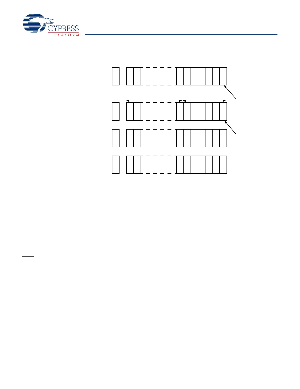
Counter Increment Operation
Once the address counter register is initially loaded with an
external address, the counter can internally increment the
address value, potentially addressing the entire memory array.
Only the unmasked bits of the counter register are incremented.
The corresponding bit in the mask register must be a “1” for a
counter bit to change. The counter register is incremented by 1
if the least significant bit is unmasked, and by 2 if it is masked. If
all unmasked bits are “1,” the next increment wraps the counter
back to the initially loaded value. If an Increment results in all the
unmasked bits of the counter being “1s,” a counter interrupt flag
(CNTINT
register to its initial value, which was stored in the mirror register.
The counter address can instead be forced to loop to 00000 by
externally connecting CNTINT
results in one or more of the unmasked bits of the counter being
“0” de-asserts the counter interrupt flag. The example in Figure
3 on page 9 shows the counter mask register loaded with a mask
value of 0003Fh unmasking the first 6 bits with bit “0” as the LSB
and bit “16” as the MSB. The maximum value the mask register
can be loaded with is 3FFFFh. Setting the mask register to this
value allows the counter to access the entire memory space. The
address counter is then loaded with an initial value of 8h. The
base address bits (in this case, the 6th address through the 16th
address) are loaded with an address value but do not increment
once the counter is configured for increment operation. The
counter address starts at address 8h. The counter increments its
internal address value till it reaches the mask register value of
3Fh. The counter wraps around the memory block to location 8h
at the next count. CNTINT
its maximum value.
) is asserted. The next Increment returns the counter
to CNTRST.
is issued when the counter reaches
[21]
An increment that
Counter Hold Operation
The value of all three registers can be constantly maintained
unchanged for an unlimited number of clock cycles. Such
operation is useful in applications where wait states are needed,
or when address is available a few cycles ahead of data in a
shared bus interface.
Counter Interrupt
The counter interrupt (CNTINT) is asserted LOW when an
increment operation results in the unmasked portion of the
counter register being all “1s.” It is deasserted HIGH when an
Increment operation results in any other value. It is also
de-asserted by Counter Reset, Counter Load, Mask Reset and
Mask Load operations, and by MRST
.
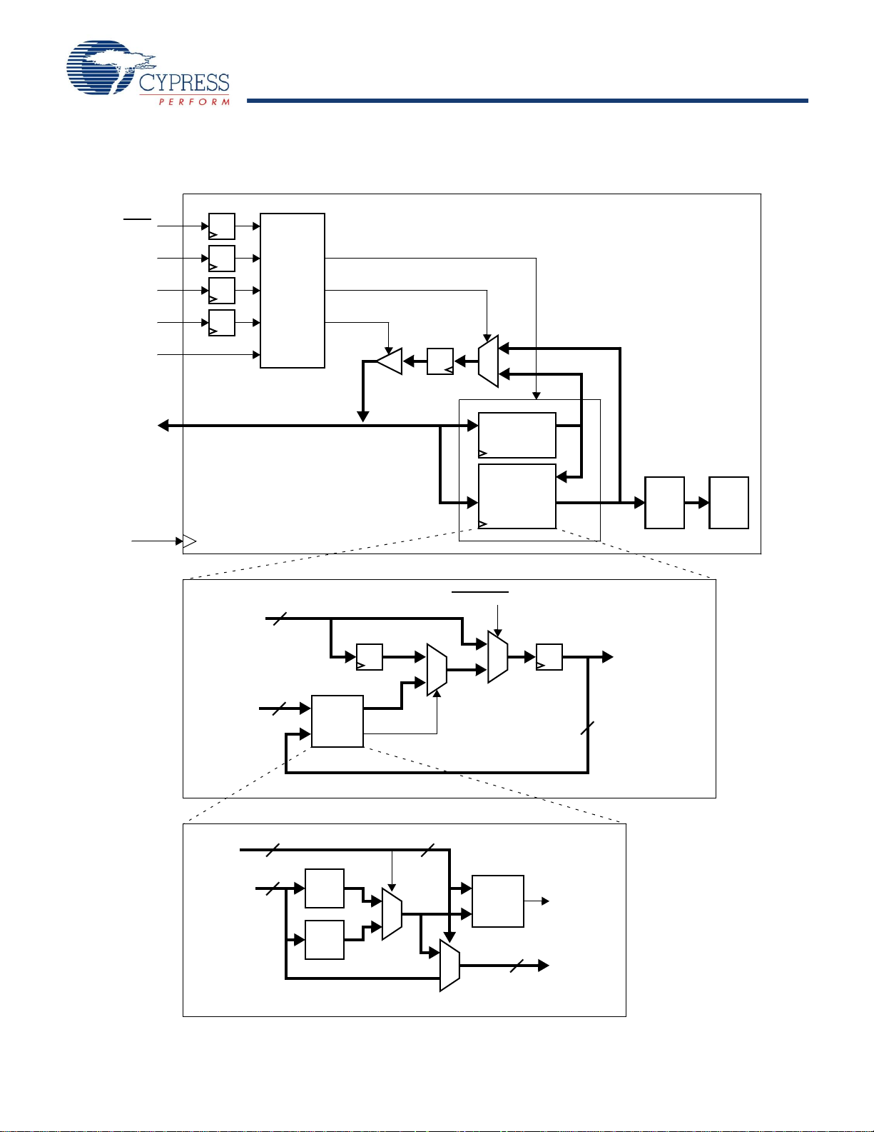
Counter Readback Operation
The internal value of the counter register can be read out on the
address lines. Readback is pipelined; the address is valid t
CA2
after the next rising edge of the port’s clock. If address readback
occurs while the port is enabled (CE0
data lines (DQs) are three-stated. Figure 2 on page 8 shows a
block diagram of the operation.
LOW and CE1 HIGH), the
Retransmit
Retransmit is a feature that allows the Read of a block of memory
more than once without the need to reload the initial address.
This eliminates the need for external logic to store and route
data. It also reduces the complexity of the system design and
saves board space. An internal “mirror register” is used to store
the initially loaded address counter value. When the counter
unmasked portion reaches its maximum value set by the mask
register, it wraps back to the initial value stored in this “mirror
register.” If the counter is continuously configured in increment
mode, it increments again to its maximum value and wraps back
to the value initially stored into the “mirror register.” Thus, the
repeated access of the same data is allowed without the need
for any external logic.
Mask Reset Operation
The mask register is reset to all “1s,” which unmasks every bit of
the counter. Master reset (MRST
to all “1s.”
) also resets the mask register
Mask Load Operation
The mask register is loaded with the address value presented at
the address lines. Not all values permit correct increment operations. Permitted values are of the form 2
most significant bit to the least significant bit, permitted values
have zero or more “0s,” one or more “1s,” or one “0.” Thus
7FFFF, 003FE, and 00001 are permitted values, but 7F0FF,
003FC, and 00000 are not.
n
– 1 or 2n – 2. From the
Mask Readback Operation
The internal value of the mask register can be read out on the
address lines. Readback is pipelined; the address is valid t
after the next rising edge of the port’s clock. If mask readback
occurs while the port is enabled (CE0
data lines (DQs) are three-stated. Figure 2 on page 8 shows a
block diagram of the operation.
LOW and CE1 HIGH), the
CM2
Counting by Two
When the least significant bit of the mask register is “0,” the
counter increments by two. This may be used to connect the x36
devices as a 72-bit single port SRAM in which the counter of one
port counts even addresses and the counter of the other port
counts odd addresses. This even-odd address scheme stores
one half of the 72-bit data in even memory locations, and the
other half in odd memory locations.
Note
21. CNTINT
Document Number: 38-06076 Rev. *G Page 7 of 28
and CNTRST specs are guaranteed by design to operate properly at speed grade operating frequency when tied together.
[+] Feedback
Page 8
CYD01S36V
CYD02S36V/36VA/CYD04S36V
CYD09S36V/CYD18S36V
From
Mask
Register
Mirror Counter
Address
Decode
RAM
Array
Wrap
1
0
Increment
Logic
1
0
+1
+2
1
0
Wrap
Detect
From
Mask
From
Counter
To
Counter
Bit 0
Wrap
Figure 2. Counter, Mask, and Mirror Logic Block Diagram
[1]
17 17
17
17
17
1
0
Load/Increment
CNT/MSK
CNTEN
ADS
CNTRST
CLK
Decode
Logic
Bidirectional
Address
Lines
Mask
Register
Counter/
Address
Register
From
Address
Lines
To Readback
and Address
Decode
17
17
MRST
Document Number: 38-06076 Rev. *G Page 8 of 28
[+] Feedback
Page 9
CYD01S36V
CYD02S36V/36VA/CYD04S36V
CYD09S36V/CYD18S36V
2162
15
2
6
2
1
2
5
2
2
242
3
2
0
2162
15
2
6
2
1
2
5
2
2
242
3
2
0
2162
15
2
6
2
1
2
5
2
2
242
3
2
0
2162
15
2
6
2
1
2
5
2
2
242
3
2
0
H
H
L
H
110s1010101
00Xs1X0X0X0
11Xs1X1X1X1
00Xs1X0X0X0
Masked Address Unmasked Address
Mask
Register
bit-0
Address
Counter
bit-0
CNTINT
Example:
Load
Counter-Mask
Register = 3F
Load
Address
Counter = 8
Max
Address
Register
Max + 1
Address
Register
Figure 3. Programmable Counter-Mask Register Operation
[1, 22]
IEEE 1149.1 Serial Boundary Scan (JTAG)
[23]
Boundary Scan Hierarchy for 9-Mbit and 18-Mbit
Devices
The FLEx36 family devices incorporate an IEEE 1149.1 serial
boundary scan test access port (TAP). The TAP controller
functions in a manner that does not conflict with the operation of
other devices using 1149.1-compliant TAPs. The TAP operates
using JEDEC-standard 3.3V IO logic levels. It is composed of
three input connections and one output connection required by
the test logic defined by the standard.
Performing a TAP Reset
A reset is performed by forcing TMS HIGH (VDD) for five rising
edges of TCK. This reset does not affect the operation of the
devices, and may be performed while the device is operating. An
MRST
must be performed on the devices after power up.
Performing a Pause/Restart
When a SHIFT-DR PAUSE-DR SHIFT-DR is performed the scan
chain outputs the next bit in the chain twice. For example, if the
value expected from the chain is 1010101, the device outputs a
11010101. This extra bit causes some testers to report an
erroneous failure for the devices in a scan test. Therefore the
tester must be configured to never enter the PAUSE-DR state.
Notes
22. The “X” in this diagram represents the counter upper bits.
23. Boundary scan is IEEE 1149.1-compatible. See “Performing a Pause/Restart” for deviation from strict 1149.1 compliance.
Document Number: 38-06076 Rev. *G Page 9 of 28
Internally, the devices have multiple DIEs. Each DIE contains all
the circuitry required to support boundary scan testing. The
circuitry includes the TAP, TAP controller, instruction register,
and data registers. The circuity and operation of the DIE
boundary scan are described in detail below.
The scan chain for 9-Mbit and 18-Mbit devices uses a hierarchical approach as shown in Figure 4 on page 10 and Figure 5
on page 10. TMS and TCK are connected in parallel to each DIE
to drive all 2- or 4-TAP controllers in unison. In many cases, each
DIE is supplied with the same instruction. In other cases, it might
be useful to supply different instructions to each DIE. One
example would be testing the device ID of one DIE while
bypassing the rest.
Each pin of the devices is typically connected to multiple DIEs.
For connectivity testing with the EXTEST instruction, it is
desirable to check the internal connections between DIEs and
the external connections to the package. This can be accomplished by merging the netlist of the devices with the netlist of the
user’s circuit board. To facilitate boundary scan testing of the
devices, Cypress provides the BSDL file for each DIE, the
internal netlist of the device, and a description of the device scan
chain. The user can use these materials to easily integrate the
devices into the board’s boundary scan environment. Further
information can be found in the Cypress application note Using
JTAG Boundary Scan For System in a Package (SIP) Dual-Port
SRAMs.
[+] Feedback
Page 10

CYD01S36V
CYD02S36V/36VA/CYD04S36V
CYD09S36V/CYD18S36V
D2
TDI
TDO
TDO
TDI
D1
TDO
TDI
D4
TDO
TDI
D3
TDO
TDI
Figure 4. Scan Chain for 18-Mbit Device
D2
TDO
TDI
D1
TDO
TDI
TDI
TDO
Figure 5. Scan Chain for 9-Mbit Device
Table 4. Identification Register Definitions
Instruction Field Value Description
Revision Number (31:28) 0h Reserved for version number.
Cypress Device ID
Cypress JEDEC ID (11:1) 034h Allows unique identification of the DP family device vendor.
ID Register Presence (0) 1 Indicates the presence of an ID register.
Table 5. Scan Register Sizes
Note
24. See details in the device BSDL files.
Document Number: 38-06076 Rev. *G Page 10 of 28
(27:12) C002h Defines Cypress part number for CYD04S36V, CYD09S36V and CYD18S36V
C001h Defines Cypress part number for CYD02S36V/36VA
C092h Defines Cypress part number for CYD01S36V
Register Name Bit Size
Instruction 4
Bypass 1
Identification 32
Boundary Scan n
[24]
[+] Feedback
Page 11

CYD01S36V
CYD02S36V/36VA/CYD04S36V
CYD09S36V/CYD18S36V
Table 6. Instruction Identification Codes
Instruction Code Description
EXTEST 0000 Captures the Input/Output ring contents. Places the BSR between the TDI and TDO.
BYPASS 1111 Places the BYR between TDI and TDO.
IDCODE 1011 Loads the IDR with the vendor ID code and places the register between TDI and TDO.
HIGHZ 0111 Places BYR between TDI and TDO. Forces all device output drivers to a High-Z state.
CLAMP 0100 Controls boundary to 1/0. Places BYR between TDI and TDO.
SAMPLE/PRELOAD 1000 Captures the input/output ring contents. Places BSR between TDI and TDO.
NBSRST 1100 Resets the non-boundary scan logic. Places BYR between TDI and TDO.
RESERVED All other codes Other combinations are reserved. Do not use other than the above.
Document Number: 38-06076 Rev. *G Page 11 of 28
[+] Feedback
Page 12

CYD01S36V
CYD02S36V/36VA/CYD04S36V
CYD09S36V/CYD18S36V
Maximum Ratings
Notes
25. The voltage on any input or IO pin cannot exceed the power pin during power up.
26. Pulse width < 20 ns.
27. I
SB1
, I
SB2
, I
SB3
and I
SB4
are not applicable for CYD18S36V because it cannot be powered down by using chip enable pins.
28. C
OUT
also references CIO.
29. Except INT
and CNTINT which are 20 pF.
Exceeding maximum ratings
device. User guidelines are not tested.
Storage Temperature.................................. –65°C to +150°C
Ambient Temperature with
Power Applied ............................................ –55°C to +125°C
Supply Voltage to Ground Potential................–0.5V to +4.6V
DC Voltage Applied to
Outputs in High-Z State .......................... –0.5V to V
DC Input Voltage .............................. –0.5V to V
[25]
may shorten the useful life of the
+0.5V
DD
+ 0.5V
DD
[26]
Electrical Characteristics Over the Operating Range
Parameter Description
V
V
V
V
I
I
I
I
OH
OL
IH
IL
OZ
IX1
IX2
CC
Output HIGH Voltage (V
Output LOW Voltage (V
= Min, IOH= –4.0 mA) 2.4 2.4 2.4 V
DD
= Min, IOL= +4.0 mA) 0.4 0.4 0.4 V
DD
Input HIGH Voltage 2.0 2.0 2.0 V
Input LOW Voltage 0.8 0.8 0.8 V
Output Leakage Current –10 10 –10 10 –10 10 μA
Input Leakage Current Except TDI, TMS, MRST –10 10 –10 10 –10 10 μA
Input Leakage Current TDI, TMS, MRST –1.0 0.1 –1.0 0.1 –1.0 0.1 mA
Operating Current for
(V
= Max.,I
DD
Disabled
= 0 mA), Outputs
OUT
CYD01S36V
CYD02S36V/
CYD02S36VA/
CYD04S36V
CYD09S36V 450 600 370 540
CYD18S36V 410 580 315 450
I
SB1
I
SB2
I
SB3
I
SB4
I
SB5
I
CORE
[27]
[27]
[27]
[27]
Standby Current (Both Ports TTL Level)
CEL and CER ≥ VIH, f = f
MAX
Standby Current (One Port TTL Level)
CEL | CER ≥ VIH, f = f
MAX
Standby Current (Both Ports CMOS Level)
CEL and CER ≥ V
– 0.2V, f = 0
DD
Standby Current (One Port CMOS Level)
CEL | CER ≥ VIH, f = f
MAX
Operating Current (VDDIO = Max,
Iout = 0 mA, f = 0) Outputs Disabled
[13]
Core Operating Current for (V
Outputs Disabled
DD
CYD18S36V 75 75 mA
= Max, I
OUT
= 0 mA),
Capacitance
Part Number Parameter
CYD01S36/
CYD02S36V/36VA/
CYD04S36V
CYD09S36V C
CYD18S36V C
C
C
C
C
IN
OUT
IN
OUT
IN
OUT
[28]
Description Test Conditions Max Unit
Input Capacitance TA = 25°C, f = 1 MHz,
Output Capacitance 10 pF
Input Capacitance 22 pF
Output Capacitance 10
Input Capacitance 40 pF
Output Capacitance 20 pF
Output Current into Outputs (LOW)............................. 20 mA
Static Discharge Voltage........................................... > 2000V
(JEDEC JESD22-A114-2000B)
Latch-up Current..................................................... > 200 mA
Operating Range
Range
Ambient
Temperature
V
DDIO/VTTL
Commercial 0°C to +70°C 3.3V±165 mV 1.8V±100 mV
Industrial –40°C to +85°C 3.3V±165 mV 1.8V±100 mV
-167 -133 -100
Min Typ. Max Min Typ. Max Min Typ. Max
225 300 225 300 mA
90 115 90 115 mA
160 210 160 210 mA
55 75 55 75 mA
160 210 160 210 mA
00 0 0 0 0mA
13 pF
VDD = 3.3V
[29]
V
CORE
[13]
pF
Unit
mA
mA
Document Number: 38-06076 Rev. *G Page 12 of 28
[+] Feedback
Page 13

CYD01S36V
CYD02S36V/36VA/CYD04S36V
CYD09S36V/CYD18S36V
Figure 6. AC Test Load and Waveforms
R1 = 590 Ω
R2 = 435 Ω
C = 5 pF
(b) Three-state Delay (Load 2)
90%
10%
3.0V
Vss
90%
10%
<2ns <2ns
ALL INPUT PULSES
3.3V
VTH = 1.5V
R = 50Ω
Z0 = 50Ω
(a) Normal Load (Load 1)
C = 10 pF
OUTPUT
OUTPUT
Note
30. Except JTAG signals (t
r
and tf < 10 ns [max.]).
Switching Characteristics Over the Operating Range
Parameter Description
f
t
t
t
t
t
t
t
t
t
t
t
t
t
t
t
t
t
t
t
t
t
t
MAX2
CYC2
CH2
CL2
[30]
R
[30]
F
SA
HA
SB
HB
SC
HC
SW
HW
SD
HD
SAD
HAD
SCN
HCN
SRST
HRST
SCM
Maximum Operating Frequency 167 133 133 100 MHz
Clock Cycle Time 6.0 7.5 7.5 10.0 ns
Clock HIGH Time 2.7 3.0 3.4 4.5 ns
Clock LOW Time 2.7 3.0 3.4 4.5 ns
Clock Rise Time 2.0 2.0 2.0 3.0 ns
Clock Fall Time 2.0 2.0 2.0 3.0 ns
Address Setup Time 2.3 2.5 2.2 2.7 ns
Address Hold Time 0.6 0.6 1.0 1.0 ns
Byte Select Setup Time 2.3 2.5 2.2 2.7 ns
Byte Select Hold Time 0.6 0.6 1.0 1.0 ns
Chip Enable Setup Time 2.3 2.5 NA NA ns
Chip Enable Hold Time 0.6 0.6 NA NA ns
R/W Setup Time 2.3 2.5 2.2 2.7 ns
R/W Hold Time 0.6 0.6 1.0 1.0 ns
Input Data Setup Time 2.3 2.5 2.2 2.7 ns
Input Data Hold Time 0.6 0.6 1.0 1.0 ns
ADS Setup Time 2.3 2.5 NA NA ns
ADS Hold Time 0.6 0.6 NA NA ns
CNTEN Setup Time 2.3 2.5 NA NA ns
CNTEN Hold Time 0.6 0.6 NA NA ns
CNTRST Setup Time 2.3 2.5 NA NA ns
CNTRST Hold Time 0.6 0.6 NA NA ns
CNT/MSK Setup Time 2.3 2.5 NA NA ns
-167 -133 -100
CYD01S36V
CYD02S36V/
CYD02S36VA
CYD04S36V
CYD09S36V
CYD01S36V
CYD02S36V
CYD04S36V
CYD09S36V
CYD18S36V CYD18S36V
Min Max Min Max Min Max Min Max
Unit
Document Number: 38-06076 Rev. *G Page 13 of 28
[+] Feedback
Page 14

CYD01S36V
CYD02S36V/36VA/CYD04S36V
CYD09S36V/CYD18S36V
Switching Characteristics Over the Operating Range (continued)
Notes
31. This parameter is guaranteed by design, but it is not production tested.
32. Test conditions used are Load 2.
-167 -133 -100
Parameter Description
t
HCM
t
OE
t
OLZ
t
OHZ
t
CD2
t
CA2
t
CM2
t
DC
t
CKHZ
t
CKLZ
t
SINT
t
RINT
t
SCINT
t
RCINT
[31, 32]
[31, 32]
[31, 32]
[31, 32]
CNT/MSK Hold Time 0.6 0.6 NA NA ns
Output Enable to Data Valid 4.4 4.4 5.5 5.5 ns
OE to Low Z 0 0 0 0 ns
OE to High Z 0 4.0 0 4.4 0 5.5 0 5.5 ns
Clock to Data Valid 4.4 4.4 5.0 5.2 ns
Clock to Counter Address Valid 4.0 4.4 NA NA ns
Clock to Mask Register Readback
Valid
Data Output Hold After Clock HIGH 1.0 1.0 1.0 1.0 ns
Clock HIGH to Output High Z 0 4.0 0 4.4 0 4.7 0 5.0 ns
Clock HIGH to Output Low Z 1.0 4.0 1.0 4.4 1.0 4.7 1.0 5.0 ns
Clock to INT Set Time 0.5 6.7 0.5 7.5 0.5 7.5 0.5 10.0 ns
Clock to INT Reset Time 0.5 6.7 0.5 7.5 0.5 7.5 0.5 10.0 ns
Clock to CNTINT Set Time 0.5 5.0 0.5 5.7 NA NA NA NA ns
Clock to CNTINT Reset time 0.5 5.0 0.5 5.7 NA NA NA NA ns
Port to Port Delays
t
CCS
Clock to Clock Skew 5.2 6.0 5.7 8.0 ns
Master Reset Timing
t
RS
t
RS
t
RSR
t
RSF
t
RSINT
Master Reset Pulse Width 5.0 5.0 5.0 5.0 cycles
Master Reset Setup Time 6.0 6.0 6.0 8.5 ns
Master Reset Recovery Time 5.0 5.0 5.0 5.0 cycles
Master Reset to Outputs Inactive 10.0 10.0 10.0 10.0 ns
Master Reset to Counter and Mailbox
Interrupt Flag Reset Time
CYD01S36V
CYD02S36V/
CYD02S36VA
CYD04S36V
CYD09S36V
Min Max Min Max Min Max Min Max
10.0 10.0 NA NA ns
CYD01S36V
CYD02S36V
CYD04S36V
CYD09S36V
4.0 4.4 NA NA ns
CYD18S36V CYD18S36V
Unit
JTAG Timing
Parameter Description
f
JTAG
t
TCYC
t
TH
t
TL
t
TMSS
t
TMSH
t
TDIS
t
TDIH
t
TDOV
t
TDOX
Document Number: 38-06076 Rev. *G Page 14 of 28
Maximum JTAG TAP Controller Frequency 10 MHz
TCK Clock Cycle Time 100 ns
TCK Clock HIGH Time 40 ns
TCK Clock LOW Time 40 ns
TMS Setup to TCK Clock Rise 10 ns
TMS Hold After TCK Clock Rise 10 ns
TDI Setup to TCK Clock Rise 10 ns
TDI Hold After TCK Clock Rise 10 ns
TCK Clock LOW to TDO Valid 30 ns
TCK Clock LOW to TDO Invalid 0 ns
167/133/100
Min Max
Unit
[+] Feedback
Page 15

CYD01S36V
CYD02S36V/36VA/CYD04S36V
CYD09S36V/CYD18S36V
JTAG Switching Waveform
Test Clock
Test Mode Select
TCK
TMS
Test Data-In
TDI
Tes t D a ta -O u t
TDO
t
TCYC
t
TMSH
t
TL
t
TH
t
TMSS
t
TDIS
t
TDIH
t
TDOX
t
TDOV
MRST
t
RSR
t
RS
INACTIVE
ACTIVE
TMS
TDO
INT
CNTINT
t
RSF
t
RSS
ALL
ADDRESS/
DATA
LINES
ALL
OTHER
INPUTS
t
RSINT
Switching Waveforms
Figure 7. Master Reset
Document Number: 38-06076 Rev. *G Page 15 of 28
[+] Feedback
Page 16

CYD01S36V
CYD02S36V/36VA/CYD04S36V
CYD09S36V/CYD18S36V
Switching Waveforms (continued)
t
CH2
t
CL2
t
CYC2
t
SC
t
HC
t
SW
t
HW
t
SA
t
HA
A
n
A
n+1
CLK
CE
R/W
ADDRESS
DATA
OUT
OE
A
n+2
A
n+3
t
SC
t
HC
t
OHZ
t
OE
t
OLZ
t
DC
t
CD2
t
CKLZ
Q
n
Q
n+1
Q
n+2
1 Latency
BE0
–BE3
t
SB
t
HB
Figure 8. Read Cycle
[14, 33, 34, 35, 36]
Notes
33. OE
is asynchronously controlled; all other inputs (excluding MRST and JTAG) are synchronous to the rising clock edge.
= CNTEN = LOW, and MRST = CNTRST = CNT/MSK = HIGH.
34. ADS
35. The output is disabled (high-impedance state) by CE
36. Addresses do not have to be accessed sequentially since ADS
Numbers are for reference only.
Document Number: 38-06076 Rev. *G Page 16 of 28
= VIH following the next rising edge of the clock.
= CNTEN = VIL with CNT/MSK = VIH constantly loads the address on the rising edge of the CLK.
[+] Feedback
Page 17

CYD01S36V
CYD02S36V/36VA/CYD04S36V
CYD09S36V/CYD18S36V
Switching Waveforms (continued)
Q
3
Q
1
Q
0
Q
2
A
0
A
1
A
2
A
3
A
4
A
5
Q
4
A
0
A
1
A
2
A
3
A
4
A
5
t
SA
t
HA
t
SC
t
HC
t
SA
t
HA
t
SC
t
HC
t
SC
t
HC
t
SC
t
HC
t
CKHZ
t
DC
t
DC
t
CD2
t
CKLZ
t
CD2
t
CD2
t
CKHZ
t
CKLZ
t
CD2
t
CKHZ
t
CKLZ
t
CD2
t
CH2
t
CL2
t
CYC2
CLK
ADDRESS
(B1)
CE
(B1)
DATA
OUT(B2)
DATA
OUT(B1)
ADDRESS
(B2)
CE
(B2)
t
CYC2
t
CL2
t
CH2
t
HC
t
SC
t
HW
t
SW
t
HA
t
SA
t
HW
t
SW
t
CD2
t
DC
tSDt
HD
WRITE
CLK
CE
R/W
ADDRESS
DATA
IN
DATA
OUT
A
n
A
n+1
A
n+2
A
n+2
D
n+2
A
n+2
A
n+3
Q
n
t
CKHZ
NO OPERATION
READ
Figure 9. Bank Select Read
[37, 38]
[36, 39, 40, 41, 42]
Figure 10. Read-to-Write-to-Read (OE = LOW)
(B2)
.
Notes
37. In this depth-expansion example, B1 represents Bank #1 and B2 is Bank #2; each bank consists of one Cypress FLEx36 device from this data sheet. ADDRESS
= ADDRESS
38. ADS
= CNTEN= BE0 – BE3 = OE = LOW; MRST = CNTRST = CNT/MSK = HIGH.
39. Output state (HIGH, LOW, or high-impedance) is determined by the previous cycle control signals.
40. During “No Operation,” data in memory at the selected address may be corrupted and must be rewritten to ensure data integrity.
41. CE
42. CE
(labelled as no operation). One clock cycle is required to three-state the IO for the Write operation on the next rising edge of CLK.
Document Number: 38-06076 Rev. *G Page 17 of 28
= OE = BE0 – BE3 = LOW; CE1 = R/W = CNTRST = MRST = HIGH.
0
= BE0 – BE3 = R/W = LOW; CE1 = CNTRST = MRST = CNT/MSK = HIGH. When R/W first switches low, since OE = LOW, the Write operation cannot be completed
0
(B1)
[+] Feedback
Page 18

CYD01S36V
CYD02S36V/36VA/CYD04S36V
CYD09S36V/CYD18S36V
Switching Waveforms (continued)
t
CYC2
t
CL2
t
CH2
t
HC
t
SC
t
HW
t
SW
t
HA
t
SA
A
n
A
n+1
A
n+2
A
n+3
A
n+4
A
n+5
t
HW
t
SW
tSDt
HD
D
n+2
t
CD2
t
OHZ
READ READWRITE
D
n+3
Q
n
CLK
CE
R/W
ADDRESS
DATA
IN
DATA
OUT
OE
Q
n+4
t
CD2
t
SA
t
HA
t
CH2
t
CL2
t
CYC2
CLK
ADDRESS
A
n
COUNTER HOLD
READ WITH COUNTER
t
SAD
t
HAD
t
SCN
t
HCN
t
SAD
t
HAD
t
SCN
t
HCN
Q
x–1
Q
x
Q
n
Q
n+1
Q
n+2
Q
n+3
t
DC
t
CD2
READ WITH COUNTER
READ
EXTERNAL
ADDRESS
ADS
CNTEN
DATA
OUT
Figure 11. Read-to-Write-to-Read (OE
Controlled)
[36, 39, 41, 42]
[41]
Figure 12. Read with Address Counter Advance
Document Number: 38-06076 Rev. *G Page 18 of 28
[+] Feedback
Page 19

CYD01S36V
CYD02S36V/36VA/CYD04S36V
CYD09S36V/CYD18S36V
Switching Waveforms (continued)
t
CH2
t
CL2
t
CYC2
A
n
A
n+1
A
n+2
A
n+3
A
n+4
D
n+1
D
n+1
D
n+2
D
n+3
D
n+4
A
n
D
n
t
SAD
t
HAD
t
SCN
t
HCN
t
SD
t
HD
WRITE EXTERNAL
WRITE WITH COUNTER
ADDRESS
WRITE WITH
COUNTER
WRITE COUNTER
HOLD
CLK
ADDRESS
INTERNAL
DATA
IN
ADDRESS
t
SA
t
HA
CNTEN
ADS
Figure 13. Write with Address Counter Advance
[42]
Document Number: 38-06076 Rev. *G Page 19 of 28
[+] Feedback
Page 20

CYD01S36V
CYD02S36V/36VA/CYD04S36V
CYD09S36V/CYD18S36V
Switching Waveforms (continued)
CLK
ADDRESS
INTERNAL
CNTEN
ADS
DATA
IN
ADDRESS
CNTRST
R/W
DATA
OUT
A
n
A
m
A
p
A
x
0
1
A
n
A
m
A
p
Q
1
Q
n
Q
0
D
0
t
CH2tCL2
t
CYC2
t
SA
t
HA
t
SW
t
HW
t
SRST
t
HRST
t
SD
t
HD
t
CD2
t
CD2
t
CKLZ
[45]
RESET ADDRESS 0
COUNTER WRITE READ
ADDRESS 0 ADDRESS 1
READ READ
ADDRESS A
n
ADDRESS A
m
READ
Figure 14. Counter Reset
[43, 44]
Notes
= BE0 – BE3 = LOW; CE1 = MRST = CNT/MSK = HIGH.
43. CE
0
44. No dead cycle exists during counter reset. A Read or Write cycle may be coincidental with the counter reset.
45. Retransmit happens if the counter remains in increment mode after it wraps to initially loaded value
Document Number: 38-06076 Rev. *G Page 20 of 28
[+] Feedback
Page 21

CYD01S36V
CYD02S36V/36VA/CYD04S36V
CYD09S36V/CYD18S36V
CNTEN
CLK
t
CH2tCL2
t
CYC2
ADDRESS
ADS
A
n
Q
x-2
Q
x-1
Q
n
t
SA
t
HA
t
SAD
t
HAD
t
SCN
t
HCN
LOAD
ADDRESS
EXTERNAL
t
CD2
INTERNAL
ADDRESS
A
n+1
A
n+2
A
n
t
CKHZ
DATA
OUT
A
n*
Q
n+3
Q
n+1
Q
n+2
A
n+3
A
n+4
t
CKLZ
t
CA2
or t
CM2
READBACK
INTERNAL
COUNTER
ADDRESS
INCREMENT
EXTERNAL
A
0–A16
Switching Waveforms (continued)
Figure 15. Readback State of Address Counter or Mask Register
[46, 47, 48, 49]
Notes
46. CE
= OE = BE0 – BE3 = LOW; CE1 = R/W = CNTRST = MRST = HIGH.
0
47. Address in output mode. Host must not be driving address bus after t
48. Address in input mode. Host can drive address bus after t
49. An * is the internal value of the address counter (or the mask register depending on the CNT/MSK
CKHZ
.
in next clock cycle.
CKLZ
level) being Read out on the address lines.
Document Number: 38-06076 Rev. *G Page 21 of 28
[+] Feedback
Page 22

CYD01S36V
CYD02S36V/36VA/CYD04S36V
CYD09S36V/CYD18S36V
t
SA
t
HA
t
SW
t
HW
t
CH2
t
CL2
t
CYC2
CLK
L
R/W
L
A
n
D
n
t
CKHZ
t
HD
t
SA
A
n
t
HA
Q
n
t
DC
t
CCS
t
SD
t
CKLZ
t
CH2
t
CL2
t
CYC2
t
CD2
L_PORT
ADDRESS
L_PORT
DATA
IN
CLK
R
R/W
R
R_PORT
ADDRESS
R_PORT
DATA
OUT
Switching Waveforms (continued)
Figure 16. Left_Port (L_Port) Write to Right_Port (R_Port) Read
[50, 51, 52]
Notes
50. CE
= OE = ADS = CNTEN = BE0 – BE3 = LOW; CE1 = CNTRST = MRST = CNT/MSK = HIGH.
0
51. This timing is valid when one port is writing, and other port is reading the same location at the same time. If t
52. If t
< minimum specified value, then R_Port Reads the most recent data (written by L_Port) only (2 * t
CCS
minimum specified value, then R_Port Reads the most recent data (written by L_Port) (t
CYC2
+ t
) after the rising edge of R_Port's clock.
CD2
Document Number: 38-06076 Rev. *G Page 22 of 28
is violated, indeterminate data is Read out.
CCS
+ t
CYC2
) after the rising edge of R_Port's clock. If t
CD2
CCS
>
[+] Feedback
Page 23

CYD01S36V
CYD02S36V/36VA/CYD04S36V
CYD09S36V/CYD18S36V
t
CH2
t
CL2
t
CYC2
CLK
3FFFD 3FFFF
INTERNAL
ADDRESS
Last_Loaded
Last_Loaded +1
t
HCM
COUNTER
3FFFE
CNTINT
t
SCINT
t
RCINT
3FFFC
CNTEN
ADS
CNT/MSK
t
SCM
Switching Waveforms (continued)
Figure 17. Counter Interrupt and Retransmit
[17, 45, 53, 54, 55, 56]
Notes
= OE = BE0 – BE3 = LOW; CE1 = R/W = CNTRST = MRST = HIGH.
53. CE
0
54. CNTINT
55. CNTINT
56. The mask register assumed to have the value of 3FFFFh.
Document Number: 38-06076 Rev. *G Page 23 of 28
is always driven.
goes LOW when the unmasked portion of the address counter is incremented to the maximum value.
[+] Feedback
Page 24

CYD01S36V
CYD02S36V/36VA/CYD04S36V
CYD09S36V/CYD18S36V
Switching Waveforms (continued)
t
CH2
t
CL2
t
CYC2
CLK
L
t
CH2
t
CL2
t
CYC2
CLK
R
7FFFF
t
SAtHA
A
n+3
A
n
A
n+1
A
n+2
L_PORT
ADDRESS
A
m
A
m+4
A
m+1
7FFFF
A
m+3
R_PORT
ADDRESS
INT
R
tSAt
HA
t
SINT
t
RINT
Figure 18. MailBox Interrupt Timing
[57, 58, 59, 60, 61]
Table 7. Read/Write and Enable Operation (Any Port)
Inputs Outputs
OE CLK CE
0
CE
1
[1, 18, 62, 63, 64]
R/W DQ0 – DQ
35
Operation
X H X X High-Z Deselected
X X L X High-Z Deselected
XLHLD
LLHHD
IN
OUT
Write
Read
H X L H X High-Z Outputs Disabled
Notes
= OE = ADS = CNTEN = LOW; CE1 = CNTRST = MRST = CNT/MSK = HIGH.
57. CE
0
58. Address “7FFFF” is the mailbox location for R_Port of the 9-Mbit device.
59. L_Port is configured for Write operation, and R_Port is configured for Read operation.
60. At least one byte enable (BE0
61. Interrupt flag is set with respect to the rising edge of the Write clock, and is reset with respect to the rising edge of the Read clock.
is an asynchronous input signal.
62. OE
63. When CE
64. CE
changes state, deselection and Read happen after one cycle of latency.
= OE = LOW; CE1 = R/W = HIGH.
0
Document Number: 38-06076 Rev. *G Page 24 of 28
– BE3) is required to be active during interrupt operations.
[+] Feedback
Page 25

CYD01S36V
CYD02S36V/36VA/CYD04S36V
CYD09S36V/CYD18S36V
Ordering Information
512K × 36 (18-Mbit) 3.3V Synchronous CYD18S36V Dual-Port SRAM
Speed(
MHz)
133 CYD18S36V-133BBC BB256B
100 CYD18S36V-100BBC BB256B
Ordering Code
CYD18S36V-133BBI BB256B
CYD18S36V-100BBI BB256B
256K × 36 (9-Mbit) 3.3V Synchronous CYD09S36V Dual-Port SRAM
Speed(
MHz)
167 CYD09S36V-167BBC BB256
133 CYD09S36V-133BBC BB256
Ordering Code
CYD09S36V-133BBI BB256
128K × 36 (4-Mbit) 3.3V Synchronous CYD04S36V Dual-Port SRAM
Speed(
MHz)
167 CYD04S36V-167BBC BB256
133 CYD04S36V-133BBC BB256
Ordering Code
CYD04S36V-133BBI BB256
64K × 36 (2-Mbit) 3.3V Synchronous CYD02S36V Dual-Port SRAM
Speed(
MHz)
167 CYD02S36V-167BBC BB256
133 CYD02S36V-133BBC BB256
Ordering Code
CYD02S36VA-167BBC BB256
CYD02S36V-133BBI BB256
32K × 36 (1-Mbit) 3.3V Synchronous CYD01S36V Dual-Port SRAM
Speed(
MHz)
167 CYD01S36V-167BBC BB256
133 CYD01S36V-133BBC BB256
Ordering Code
CYD01S36V-133BBI BB256
Package
Name
Package
Name
Package
Name
Package
Name
Package
Name
Package Type
256-ball Grid Array 23 mm × 23 mm with 1.0-mm pitch (BGA)
256-ball Grid Array 23 mm × 23 mm with 1.0-mm pitch (BGA)
256-ball Grid Array 23 mm × 23 mm with 1.0-mm pitch (BGA)
256-ball Grid Array 23 mm × 23 mm with 1.0-mm pitch (BGA)
Package Type
256-ball Grid Array 17 mm × 17 mm with 1.0-mm pitch (BGA)
256-ball Grid Array 17 mm × 17 mm with 1.0-mm pitch (BGA)
256-ball Grid Array 17 mm × 17 mm with 1.0-mm pitch (BGA)
Package Type
256-ball Grid Array 17 mm × 17 mm with 1.0-mm pitch (BGA)
256-ball Grid Array 17 mm × 17 mm with 1.0-mm pitch (BGA)
256-ball Grid Array 17 mm × 17 mm with 1.0-mm pitch (BGA)
Package Type
256-ball Grid Array 17 mm × 17 mm with 1.0-mm pitch (BGA)
256-ball Grid Array 17 mm × 17 mm with 1.0-mm pitch (BGA)
256-ball Grid Array 17 mm × 17 mm with 1.0-mm pitch (BGA)
256-ball Grid Array 17 mm × 17 mm with 1.0-mm pitch (BGA)
Package Type
256-ball Grid Array 17 mm × 17 mm with 1.0-mm pitch (BGA)
256-ball Grid Array 17 mm × 17 mm with 1.0-mm pitch (BGA)
256-ball Grid Array 17 mm × 17 mm with 1.0-mm pitch (BGA)
Operating
Range
Commercial
Industrial
Commercial
Industrial
Operating
Range
Commercial
Commercial
Industrial
Operating
Range
Commercial
Commercial
Industrial
Operating
Range
Commercial
Commercial
Industrial
Operating
Range
Commercial
Commercial
Industrial
Document Number: 38-06076 Rev. *G Page 25 of 28
[+] Feedback
Page 26

CYD01S36V
CYD02S36V/36VA/CYD04S36V
CYD09S36V/CYD18S36V
Package Diagrams
BOTTOM VIEW
TOP VIEW
10987654321
A
B
C
D
E
F
G
H
J
K
PIN 1 CORNER
PIN 1 CORNER
0.20(4X)
Ø0.25MCAB
Ø0.05 M C
Ø0.45±0.05(256X)-CPLD DEVICES (37K & 39K)
0.25 C
0.70±0.05
C
SEATING PLANE
0.15 C
16 15 14 13 12 11
T
R
P
M
N
L
N
T
R
P
M
L
K
J
F
G
H
E
D
A
C
B
161513 141210 11928765431
A
B
Ø0.50 (256X)-ALL OTHER DEVICES
+0.10
-0.05
A1 0.36 0.56
A 1.40 MAX. 1.70 MAX.
REFERENCE JEDEC MO-192
15.00
1.00
0.35
A
17.00±0.10
7.50
7.50
15.00
17.00±0.10
1.00
A1
-0.05
+0.10
51-85108-*F
Figure 19. 256-Ball FBGA (17 x 17 mm) BB256
Document Number: 38-06076 Rev. *G Page 26 of 28
[+] Feedback
Page 27

CYD01S36V
CYD02S36V/36VA/CYD04S36V
CYD09S36V/CYD18S36V
Package Diagrams (continued)
TOP VIEW
15.00
1.00
10 9 8 7 6 5 4 3 2 1
A
B
C
D
E
F
G
H
J
K
PIN 1 CORNER
PIN 1 CORNER
0.20(4X)
Ø0.25 M C A B
Ø0.05 M C
0.25 C
0.70±0.05
C
SEATING PLANE
0.15 C
0.35
16 15 14 13 12 11
T
R
P
M
N
L
N
T
R
P
M
L
K
J
F
G
H
E
D
A
C
B
161513 141210 11928765431
23.00±0.10
A
B
7.50
7.50
15.00
23.00±0.10
1.00
Ø0.50 (256X)
-0.05
+0.10
+0.10
-0.05
1.70 MAX.
0.56
JEDEC MO-192
51-85201-*A
Figure 20. 256-ball FBGA (23 mm x 23 mm x 1.7 mm) BB256B
Document Number: 38-06076 Rev. *G Page 27 of 28
[+] Feedback
Page 28

CYD01S36V
CYD02S36V/36VA/CYD04S36V
CYD09S36V/CYD18S36V
Document History Page
Document Title: CYD01S36V CYD02S36V/36VA/CYD04S36V CYD09S36V/CYD18S36V FLEx36™ 3.3V
32K/64K/128K/256K/512 x 36 Synchronous Dual-Port RAM
Document Number: 38-06076
REV. ECN NO.
Orig. of
Change
Submission
Date
Description of Change
** 232012 WWZ See ECN New data sheet
*A 244232 WWZ See ECN Changed pinout
Changed FTSEL# to FTSEL
in the block diagram
*B 313156 YDT See ECN Changed pinout D10 from NC to VSS to reflect test mode pin swap, C10 from
rev[2,4] to VSS to reflect SC removal.
Changed tRSCNTINT to tRSINT
Added tRSINT to the master reset timing diagram
Added CYD01S36V to data sheet
Added I
and changed I
SB5
IX2
*C 321033 YDT See ECN Added CYD18S36V-133BBI to the Ordering Information Section
*D 327338 AEQ See ECN Change Pinout C10 from VSS to NC[2,5]
Change Pinout G5 from VDDIOL to REVL[2,3]
*E 365315 YDT See ECN Added note for V
Removed preliminary status
*F 2193427 NXR/AESA See ECN Changed t
Template Update.
CD2
CORE
and t
Spec from 4ns to 4.4ns for -167.
OE
*G 2623658 VKN/PYRS 12/17/08 Added CYD02S36VA-15AXC part
Sales, Solutions and Legal Information
Worldwide Sales and Design Support
Cypress maintains a worldwide network of offices, solution centers, manufacturer’s representatives, and distributors. To find the office
closest to you, visit us at cypress.com/sales.
Products
PSoC psoc.cypress.com
Clocks & Buffers clocks.cypress.com
Wireless wireless.cypress.com
Memories memory.cypress.com
Image Sensors image.cypress.com
© Cypress Semiconductor Corporation, 2005-2008. The information contained herein is subject to change without notice. Cypress Semiconductor Corporation assumes no responsibility for the use of
any circuitry other than circuitry embodied in a Cypress product. Nor does it convey or imply any license under patent or other rights. Cypress products are not warranted nor intended to be used fo r
medical, life support, life saving, critical control or safety applications, unless pursuant to an express written agreement with Cypress. Furthermore, Cypress does not authorize its products for use as
critical components in life-support systems where a malfunction or failure may reasonably be expected to result in significant injury to the user. The inclusion of Cypress products in life-support systems
application implies that the manufacturer assumes all risk of such use and in doing so indemnifies Cypress against all charges.
Any Source Code (software and/or firmware) is owned by Cypress Semiconductor Corporation (Cypress) and is protected by and subject to worldwide patent protection (United States and foreign),
United States copyright laws and international treaty provisions. Cypress hereby grants to licensee a personal, non-exclusive, non-transferable license to copy, use, modify, create derivative works of,
and compile the Cypress Sou rce Code and derivative works for the sole purpose of cr eating custom software and or firmware in support of licensee product to be used only in conjunction with a Cypress
integrated circuit as specified in the applicable agreement. Any reproduction, modification, translation, compilation, or representation of this Source Code except as specified above is prohibited without
the express written permission of Cypress.
Disclaimer: CYPRESS MAKES NO WARRANTY OF ANY KIND, EXPRESS OR IMPLIED, WITH REGARD TO THIS MATERIAL, INCLUDING, BUT NOT LIMITED TO, THE IMPLIED WARRANTIES
OF MERCHANTABILITY AND FITNESS FOR A PARTICULAR PURPOSE. Cypress reserves the right to make changes without further notice to the materials described herein. Cypress does not
assume any liability arising out of the application or use of any product or circuit described herein. Cypress does not authorize its products for use as critical components in life-support systems where
a malfunction or failure may reasonably be expected to result in significant injury to the user. The inclusion of Cypress’ product in a life-support systems application implies that the manufacturer
assumes all risk of such use and in doing so indemnifies Cypress against all charges.
Use may be limited by and subject to the applicable Cypress software license agreement.
PSoC Solutions
General psoc.cypress.com/solutions
Low Power/Low Voltage psoc.cypress.com/low-power
Precision Analog psoc.cypress.com/precision-analog
LCD Drive psoc.cypress.com/lcd-drive
CAN 2.0b psoc.cypress.com/can
USB psoc.cypress.com/usb
Document Number: 38-06076 Rev. *G Revised Decenber 09, 2008 Page 28 of 28
FLEx36 and FLEx36-E are trademarks of Cypress Semiconductor Corporation. All other trademarks or registered trademarks referenced herein are property of the respective corporations. All products
and company names mentioned in this document may be the trademarks of their respective holders.
[+] Feedback
 Loading...