
Features
CY8CLED16
EZ-Color™ HB LED Controller
■ HB LED Controller
❐ Configurable Dimmers Support up to 16
Independent LED Channels
❐ 8-32 Bits of Resolution per Channel
❐ Dynamic Reconfiguration Enables LED
Controller plus other Features; Battery
Charging, Motor Control…
■ Visual Embedded Design, PSoC Express
❐ LED Based Express Drivers
• Binning Compensation
• Temperature Feedback
•DMX512
■ PrISM Modulation Technology
❐ Reduces Radiated EMI
❐ Reduces Low Frequency Blinking
■ Powerful Harvard Architecture Processor
❐ M8C Processor Speeds to 24 MHz
❐ 3.0 to 5.25V Operating Voltage
❐ Operating Voltages down to 1.0V using
On-Chip Switch Mode Pump (SMP)
❐ Industrial Temperature Range: -40°C to +85°C
■ Programmable Pin Configur ations
❐ 25 mA Sink on all GPIO
❐ Pull up, Pull down, High Z, Strong, or Open Drain Drive
Modes on all GPIO
❐ Up to eight Analog Inputs on GPIO
❐ Configurable Interrupt on all GPIO
■ Advanced Peripherals (PSoC Blocks)
❐ 16 Digital PSoC Blocks Provide:
• 8 to 32-Bit Timers, Counters, and PWMs
• Up to 2 Full-Duplex UART
• Multiple SPI™ Masters or Slaves
• Connectable to all GPIO Pins
❐ 12 Rail-to-Rail Analog PSoC Blocks Provide:
• Up to 14-Bit ADCs
• Up to 9-Bit DACs
• Programmable Gain Amplifiers
• Programmable Filters and Comparators
❐ Complex Peripherals by Combining Blocks
■ Flexible On-Chip Memory
❐ 32K Flash Program Storage 50,000 Erase/Write Cycles
❐ 2K SRAM Data Storage
❐ In-System Serial Programming (ISSP)
❐ Partial Flash Updates
❐ Flexible Protection Modes
❐ EEPROM Emulation in Flash
■ Complete Development Tools
❐ Free Development Software
• PSoC Designer™
• PSoC Express™
❐ Full-Featured, In-Circuit Emulator and
Programmer
❐ Full Speed Emulation
❐ Complex Breakpoint Structure
❐ 128 KBytes Trace Memory
EZ-Color HB LED Controller
Preliminary Data Sheet
Cypress Semiconductor Corporation •198 Champion Court•San Jose, CA 95134-1709•408-943-2600
Document Number: 001-13105 Rev. ** Revised June 12, 2007
Overview
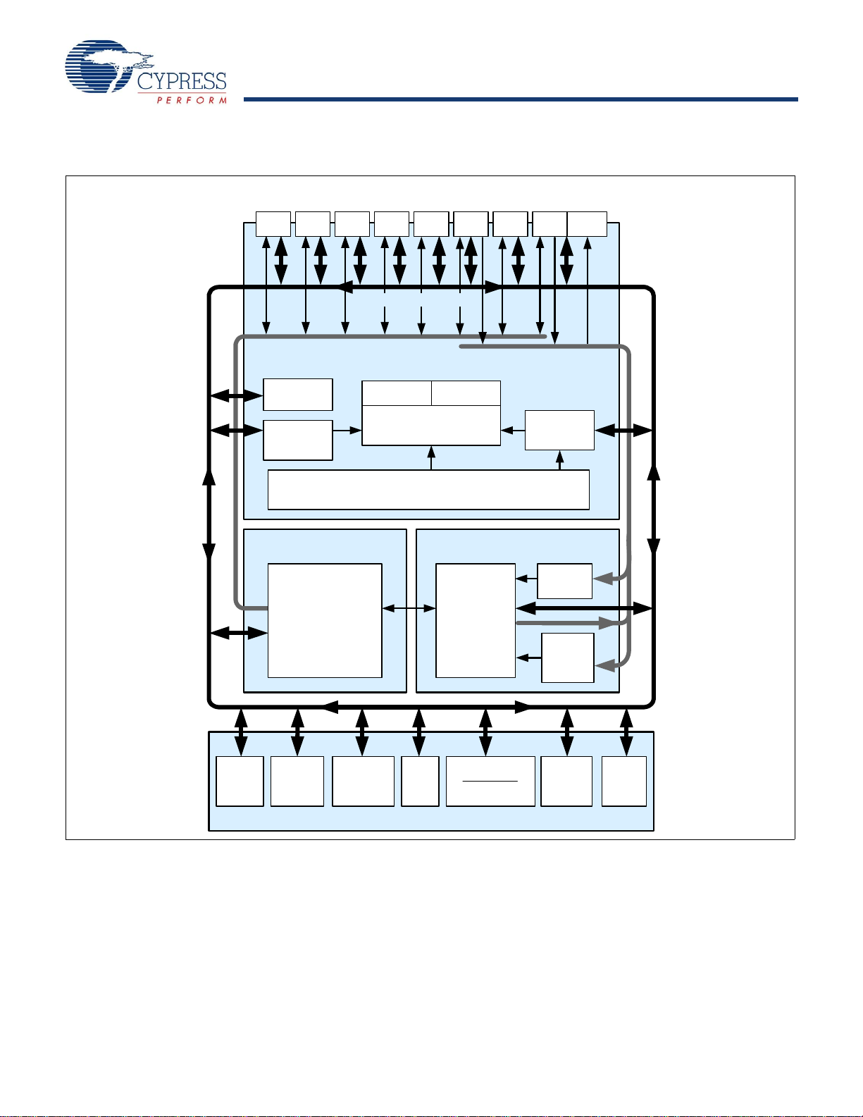
Block Diagram
Port 7 Port 6 Port 5 Port 4 Port 3 Port 2 Port 1 Port 0
SYSTEM BUS
CY8CLED16
Analog
Drivers
Global Digital Interconnect
SRAM
2K
Interrupt
Controller
SROM Flash 32K
CPU Core (M8C)
Multiple Clock Sources
(Includes IMO, ILO, PLL, and ECO)
DIGITAL SYSTEM
Digital
Block
Array
Global Analog Interconnect
PSoC CORE
Sleep and
Watchdog
ANALOG SYSTEM
Analog
Ref.
Analog
Block
Array
Analog
Input
Muxing
Digital
Clocks
Two
Multiply
Accums.
Decimator
2
I C
POR and LVD
System Resets
Internal
Voltage
Ref.
Switch
Mode
Pump
SYSTEM RESOURCES
Document Number: 001-13105 Rev. ** Page 2 of 39

CY8CLED16
EZ-Color Functional Overview
Cypress' EZ-Color family of devices offers the ideal control
solution for High Brightness LED applications requiring intelligent dimming control. EZ-Color devices combine the power and
flexibility of PSoC (Programmable System-on-Chip™); with
Cypress' PrISM (precise illumination signal modulation)
modulation technology providing lighting designers a fully
customizable and integrated lighting solution platform.
The EZ-Color family supports up to 16 independent LED
channels with up to 32 bits of resolution per channel, enabling
lighting designers the flexibility to choose the LED array size and
color quality. PSoC Express software, with lighting specific
drivers, can significantly cut development time and simplify
implementation of fixed color points through temperature and
LED binning compensation. EZ-Color's virtually limitless analog
and digital customization allow for simple integration of features
in addition to intelligent lighting, such as Battery Charging, Image
Stabilization, and Motor Control during the development
process. These features, along with Cypress' best-in-class
quality and design support, make EZ-Color the ideal choice for
intelligent HB LED control applications.
Target Applications
■ LCD Backlight
■ Large Signs
■ General Lighting
■ Architectural Lighting
■ Camera/Cell Phone Flash
■ Flashlights
The PSoC Core
The PSoC Core is a powerful engine that supports a rich feature
set. The core includes a CPU, memory , clocks, and configurable
GPIO (General Purpose IO).
The M8C CPU core is a powerful processor with speeds up to 48
MHz, providing a four MIPS 8-bit Harvard architecture microprocessor. The CPU utilizes an interrupt controller with 25 vectors,
to simplify programming of real time embedded events. Program
execution is timed and protected using the included Sle ep and
Watch Dog Timers (WDT).
Memory encompasses 32 KB of Flash for program storage, 2 KB
of SRAM for data storage, and up to 2 KB of EEPROM emulated
using the Flash. Program Flash utilizes four protection levels on
blocks of 64 bytes, allowing customized software IP protection.
The EZ-Color family incorporates flexible internal clock generators, including a 24 MHz IMO (int ernal main oscill ator) accurate
to 2.5% over temperature and voltage. The 24 MHz IMO can also
be doubled to 48 MHz for use by the digital system. A low power
32 kHz ILO (internal low speed oscillator) is provided for the
Sleep timer and WDT. If crystal accuracy is desired, the ECO
(32.768 kHz external crystal oscillator) is available for use as a
Real Time Clock (RTC) and can optionally generate a
crystal-accurate 24 MHz system clock using a PLL. The clocks,
together with programmable clock dividers (as a System
Resource), provide the flexibility to integrate almost any timing
requirement into the EZ-Color device.
EZ-Color GPIOs provide connection to the CPU, digital and
analog resources of the device. Each pin’s drive mode may be
selected from eight options, allowing great flexibility in external
interfacing. Every pin also has the capability to generate a
system interrupt on high level, low level, and change from last
read.
The Digital System
The Digital System is composed of 16 digital PSoC blocks. Each
block is an 8-bit resource that can be used alone or combined
with other blocks to form 8, 16, 24, and 32-bit peripherals, which
are called user module references. Digital peripheral configurations include those listed below.
■ PrISM (8 to 32 bit)
■ PWMs (8 to 32 bit)
■ PWMs with Dead band (8 to 32 bit)
■ Counters (8 to 32 bit)
■ Timers (8 to 32 bit)
■ UART 8 bit with selectable parity (up to 4)
■ SPI master and slave (up to 4 each)
■ I2C slave and multi-master (1 available as a System Resource)
■ Cyclical Redundancy Checker/Generator (8 to 32 bit)
■ IrDA (up to 4)
■ Generators (8 to 32 bit)
The digital blocks can be connected to any GPIO through a
series of global buses that can route any signal to any pin. The
buses also allow for signal multiplexing and for performing logic
operations. This configurability frees your designs from the
constraints of a fixed peripheral controller.
Digital blocks are provided in rows of four, where the number of
blocks varies by EZ-Color device family. This allows you the
optimum choice of system resources for your application. Family
resources are shown in the table titled EZ-Color Device Characteristics on page 4.
Document Number: 001-13105 Rev. ** Page 3 of 39
CY8CLED16
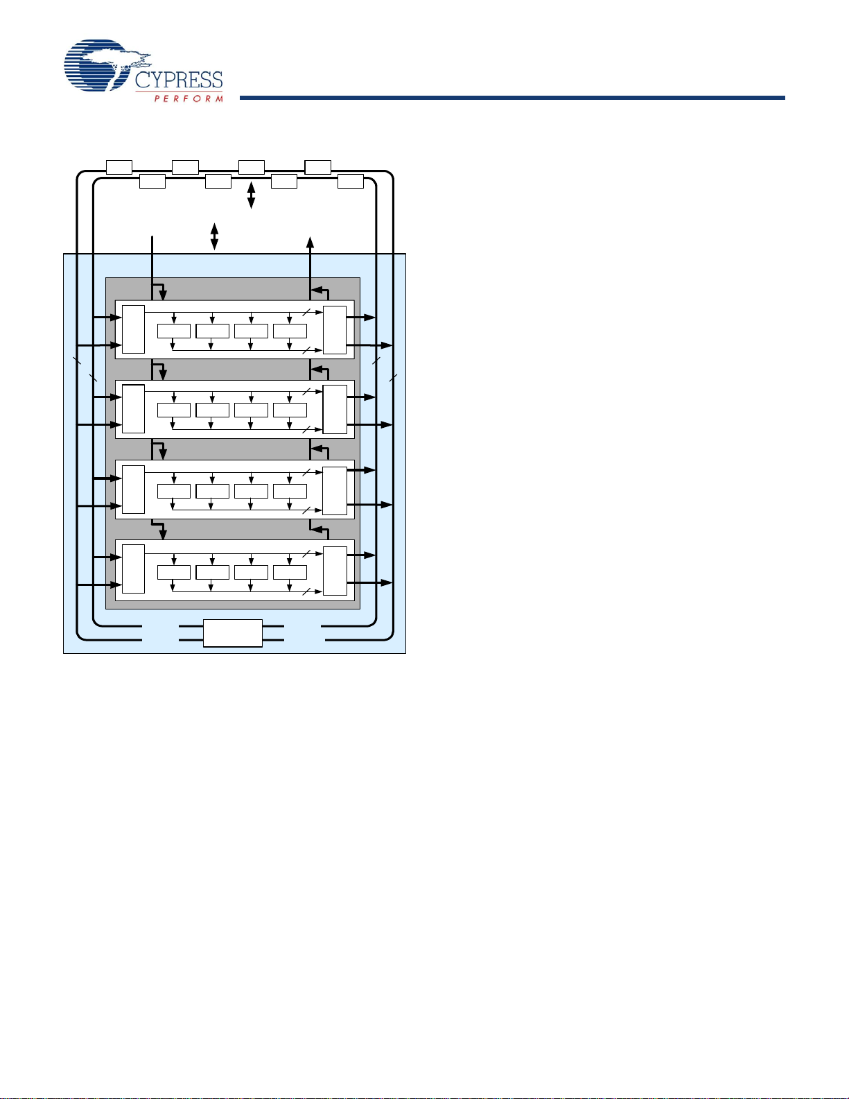
Figure 1. Digital System Block Diagram
Port 7
Port 6
Port 5
Port 4
Port 3
Port 2
Port 1
Port 0
The Analog System
The Analog System is composed of 12 configurable blocks, each
comprised of an opamp circuit allowing the creation of complex
analog signal flows. Analog peripherals are very flexible and can
l
o
c
k
o
r
e
To System Bus
s
To Analog
System
D
i
g
i
t
a
l
C
F
r
C
o
m
DIGITAL SYSTEM
Digital PSoC Block Array
Row 0
DBB00 DBB01 DCB02 DCB03
Row Input
8
Configuration
Row 1
DBB10 DBB11 DCB12 DCB13
Row Input
Configuration
Configuration
Row Output
4
4
8
Configuration
4
Row Output
4
be customized to support specific application requirements.
Some of the more common EZ-Color analog functions (most
available as user modules) are listed below.
■ Analog-to-digital converters (up to 4, with 6- to 14-bit resolution,
selectable as Incremental, Delta Sigma, and SAR)
■ Filters (2, 4, 6, or 8 pole band-pass, low-pass, and notch)
■ Amplifiers (up to 4, with selectable gain to 48x)
■ Instrumentation amplifiers (up to 2, with selectable gain to 93x)
■ Comparators (up to 4, with 16 selectable thresholds)
88
■ DACs (up to 4, with 6- to 9-bit resolution)
■ Multiplying DACs (up to 4, with 6- to 9-bit resolution)
■ High current output drivers (four with 40 mA drive as a Core
Resource)
Row 2
DBB20 DBB21 DCB22 DCB23
Row Input
Configuration
Row 3
DBB30 DBB31 DCB32 DCB33
Row Input
Configuration
Configuration
4
Row Output
4
Configuration
Row Output
4
4
■ 1.3V reference (as a System Resource)
■ DTMF Dialer
■ Modulators
■ Correlators
■ Peak Detectors
■ Many other topologies possible
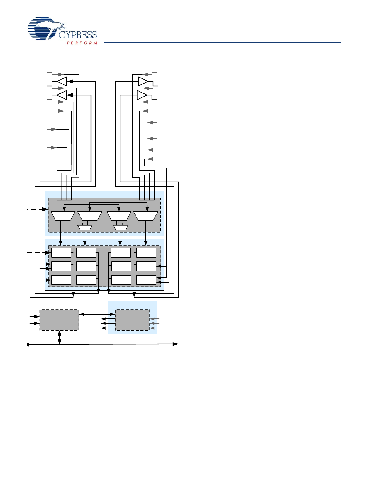
Analog blocks are provided in columns of three, which includes
one CT (Continuous Time) and two SC (Switched Capacitor)
GIE[7:0]
GIO[7:0]
Global D ig ital
Interconnect
GOE[7:0]
GOO[7:0]
blocks, as shown in the figure below.
Document Number: 001-13105 Rev. ** Page 4 of 39
CY8CLED16
P0[7]
P0[5]
P0[3]
P0[1]
P2[3]
P2[1]
Figure 2. Analog System Block Diagram
RefIn
AGNDIn
Array Input Configuration
ACI0[1:0 ] ACI3[1:0 ]
ACB00 ACB01
ACI1[1:0] ACI2[1:0]
Block Array
ACB02 ACB03
P0[6]
P0[4]
P0[2]
P0[0]
P2[6]
P2[4]
P2[2]
P2[0]
Additional System Resources
System Resources, some of which have been previously listed,
provide additional capability useful to complete systems.
Resources include a multiplier, decimator, switch mode pump,
low voltage detection, and power on reset. Statements
describing the merits of each system resource are presented
below.
■ Digital clock dividers provide three customizable clock
frequencies for use in applications. The clocks can be routed
to both the digital and analog systems. Additional clocks can
be generated using digital PSoC blocks as clock dividers.
■ Multiply accumulate (MAC) provides fast 8-bit multiplier with
32-bit accumulate, to assist in general math and digital filters.
■ The decimator provides a custom hardware filter for digital
signal, processing applications including the creation of Delta
Sigma ADCs.
■ The I2C module provides 100 and 400 kHz communication over
two wires. Slave, master, and multi-master modes are all
supported.
■ Low Voltage Detection (LVD) interrupts can signal the appli-
cation of falling voltage levels, while the advanced POR (Power
On Reset) circuit eliminates the need for a system supervisor.
■ An internal 1.3 voltage reference provides an absolute
reference for the analog system, including ADCs and DACs.
■ An integrated switch mode pump (SMP) generates normal
operating voltages from a single 1.2V battery cell, providing a
low cost boost converter.
ASC10
Interface to
Digital System
M8C Interface (Address Bus, Data Bus, Etc.)
ASD11
ASC21
AGND
RefHi
RefLo
ASC12 ASD13
ASD22 ASC23ASD20
Analog Reference
Reference
Generators
AGNDIn
RefIn
Bandgap
Document Number: 001-13105 Rev. ** Page 5 of 39
CY8CLED16
EZ-Color Device Characteristics
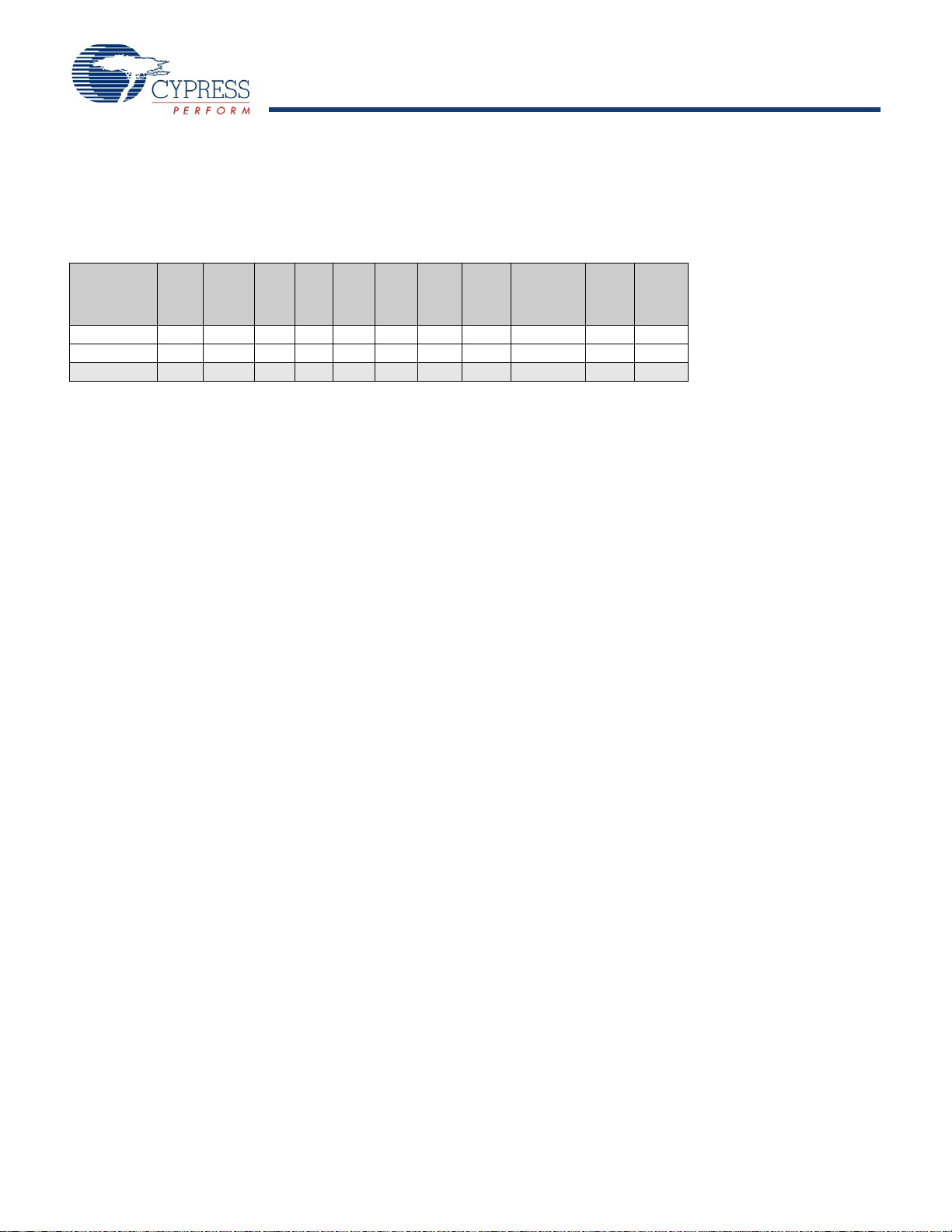
Depending on your EZ-Color device characteristics, the digital and analog systems can have 16, 8, or 4 digital blocks and 12, 6, or 4
analog blocks. The following table lists the resources available for specific EZ-Color device groups. The device covered by this data
sheet is shown in the highlighted row of the table.
Table 1. EZ-Color Device Characteristics
PSoC Part
Number
CY8CLED04 4 56 1 4 48 2 2 6 1K 16K Yes
CY8CLED08 8 44 2 8 12 4 4 12 256 Bytes 16K No
CY8CLED16 16 64 4 16 12 4 4 12 2K 32K No
LED
Channels
IO
Digital
Rows
Digital
Digital
Blocks
Analog
Inputs
Analog
Analog
Outputs
Columns
Analog
Blocks
Size
SRAM
Size
Flash
Getting Started
The quickest path to understanding the EZ-Color silicon is by
reading this data sheet and using PSoC Express to create HB
LED applications. This data sheet is an overview of the EZ-Color
integrated circuit and presents specific pin, register, and
electrical specifications.
For up-to-date Ordering, Packaging, and Electrical Specification
information, reference the latest device data sheets on the web
at http://www.cypress.com/ez-color.
Development Kits
Development Kits are available from the following distributors:
Digi-Key, A vnet, Arrow , and Future. The Cypress Online Store at
http://www.onfulfillment.com/cypressstore/ contains devel-
opment kits, C compilers, and all accessories for PSoC development. Click on EZ-Color to view a current list of available
items.
Technical Training Modules
Free PSoC technical training modules are available for users
new to PSoC. Training modules cover designing, debugging,
advanced analog, CapSense, and HB LED. Go to
http://www.cypress.com/techtrain.
Consultants
Certified PSoC Consultants offer everything from technical
assistance to completed PSoC designs. To contact or become a
PSoC Consultant, go to the following Cypress support web site:
http://www.cypress.com/support/cypros.cfm.
Technical Support
PSoC application engineers take pride in fast and accurate
response. They can be reached with a 4-hour guaranteed
response at http://www.cypress.com/support/login.cfm.
Application Notes
A long list of application notes will assist you i n every aspe ct of
your design effort. To view the PSoC application notes, go to the
http://www.cypress.com web site and select Application Notes
under the Design Resources list located in the center of the web
page. Application notes are listed by date by default.
CapSense
Document Number: 001-13105 Rev. ** Page 6 of 39
CY8CLED16
Development Tools
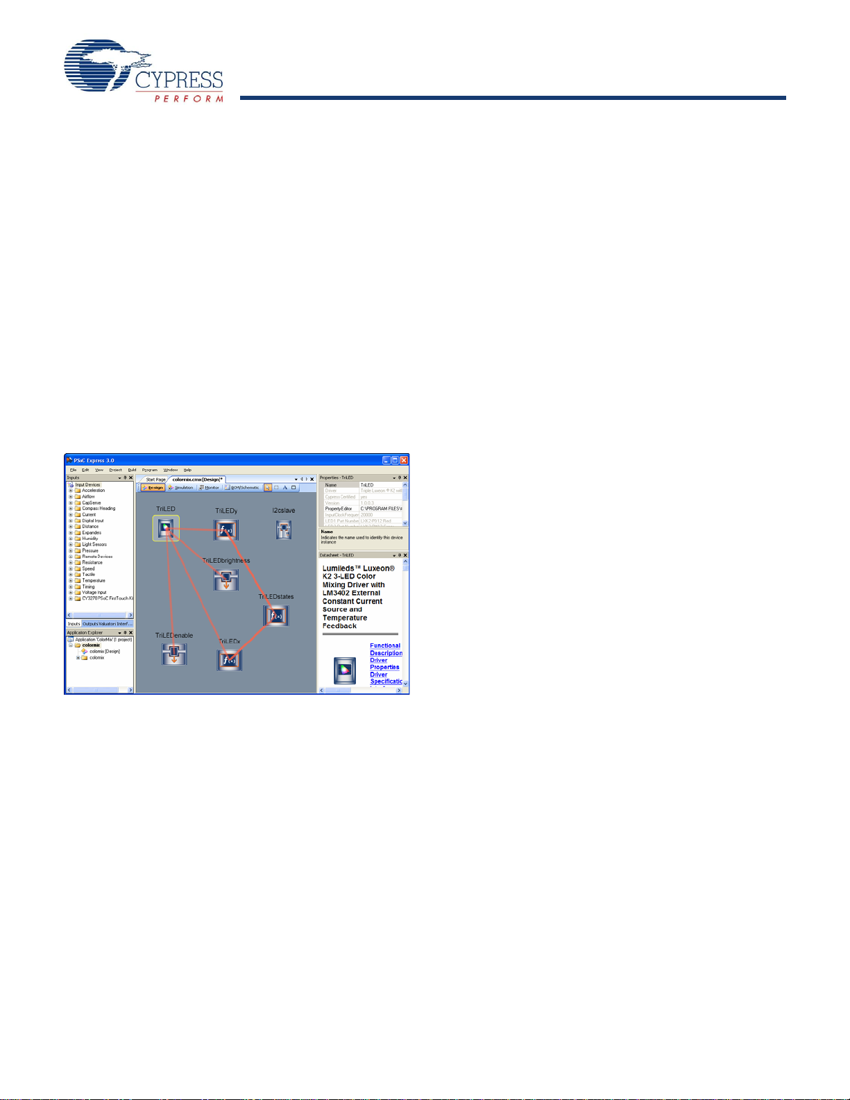
PSoC Express is a high-level design tool for creating embedded
systems with devices using Cypress's PSoC Mixed-Signal
technology. With PSoC Express you create a complete
embedded solution including all necessary on-chip peripherals,
block configuration, interrupt handling and application software
without writing a single line of assembly or C code.
PSoC Express solves design problems the way you think about
the system:
■ Select input and output devices based upon system require-
ments.
■ Add a communications interface and define its interface to
system (using registers).
■ Define when and how an output device chang es state based
upon any and all other system devices.
■ Based upon the design, automatically select one or more PSoC
Mixed-Signal Controllers that match system requirements.
Figure 3. PSoC Express
Most of the files associated with a project are automatically
generated by PSoC Express during the build process, but you
can make changes directly to the custom.c and custom.h files
and also add your own custom code to the project in the Project
Manager.
Application Editor
The Application Editor allows you to edit custom.c and custom.h
as well as any C or assembly language source code that you add
to your project. With PSoC Express you can create application
software without writing a single line of assembly or C code, but
you have a full featured application editor at your finger tips if you
want it.
Build Manager
The Build Manager gives you the ability to build the application
software, assign pins, and generate the data sheet, schematic,
and BOM for your project.
Board Monitor
The Board Monitor is a debugging tool designed to be used
while attached to a prototype board through a communication
interface that allows you to monitor changes in the various
design elements in real time.
The default communication for the board monitor is I
2
the CY3240-I2USB I
C to USB Bridge Debugging/Communica-
tion Kit.
2
C. It uses
PSoC Express Subsystems
Express Editor
The Express Editor allows you to create designs visually by
dragging and dropping inputs, outputs, communication interfaces, and other design elements, and then describing the logic
that controls them.
Project Manager
The Project Manager allows you to work with your applications
and projects in PSoC Express. A PSoC Express application is a
top level container for projects and their associated files. Each
project contains a design that uses a single PSoC device. An
application can contain multiple projects so if you are creating an
application that uses multiple PSoC devices you can keep all of
the projects together in a single application.
Tuners
A Tuner is a visual interface for the Board Monitor that allows
you to view the performance of the HB LED drivers on your test
board while your program is running, and manually override values and see the results.
Hardware Tools
In-Circuit Emulator
A low cost, high functionality ICE (In-Circuit Emulator) is
available for development support. This hardware has the
capability to program single devices.
The emulator consists of a base unit that connects to the PC by
way of the USB port. The base unit is universal and will operate
with all PSoC devices. Emulation pods for each device family are
available separately. The emulation pod takes the place of the
PSoC device in the target board and performs full speed (24
MHz) operation.
2
I
C to USB Bridge
2
C to USB Bridge is a quick and easy link from any design
The I
or application’s I
debugging and communication.
2
C bus to a PC via USB for design testing,
Document Number: 001-13105 Rev. ** Page 7 of 39

Document Conventions
CY8CLED16
Acronyms Used
The following table lists the acronyms that are used in this
document.
Acronym Description
AC alternating current
ADC analog-to-digital converter
API application programming interface
CPU central processing unit
CT continuous time
DAC digital-to-analog converter
DC direct current
ECO external crystal oscillator
EEPROM electrically erasable programmable read-only memory
FSR full scale range
GPIO general purpose IO
GUI graphical user interface
HBM human body model
ICE in-circuit emulator
ILO internal low speed oscillator
IMO internal main oscillator
IO input/output
IPOR imprecise power on reset
LSb least-significant bit
LVD low voltage detect
MSb most-significant bit
PC program counter
PLL phase-locked loop
POR power on reset
PPOR precision power on reset
PSoC™ Programmable System-on-Chip™
PWM pulse width modulator
SC switched capacitor
SLIMO slow IMO
SMP switch mode pump
SRAM static random access memory
Units of Measure
A units of measure table is located in the Electrical Specifications
section. Table 7 on page 15 lists all the abbreviations used to
measure the PSoC devices.
Numeric Naming
Hexidecimal numbers are represented with all letters in
uppercase with an appended lowercase ‘h’ (for example, ‘14h’ or
‘3Ah’). Hexidecimal numbers may also be represented by a ‘0x’
prefix, the C coding convention. Binary numbers have an
appended lowercase ‘b’ (e.g., 01010100b’ or ‘01000011b’).
Numbers not indicated by an ‘h’, ‘b’, or 0x are decimal.
Document Number: 001-13105 Rev. ** Page 8 of 39

CY8CLED16
Pin Information
Pinouts
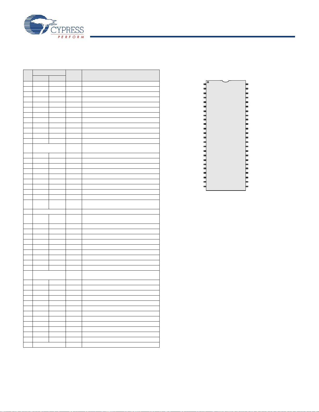
The CY8CLED16 device is available in three packages which are listed and illustrated in the following tables. Every port pin (labeled
with a “P”) is capable of Digital IO. However, Vss, Vdd, SMP, and XRES are not capable of Digital IO.
28-Pin Part Pinout
Table 2. 28-Pin Part Pinout (SSOP)
Pin
No.
1 IO I P0[7] Analog column mux input.
2 IO IO P0[5] Analog column mux input and column output.
3 IO IO P0[3] Analog column mux input and column output.
4 IO I P0[1] Analog column mux input.
5 IO P2[7]
6 IO P2[5]
7 IO I P2 [3 ] Direct switched capacitor block input.
8 IO I P2 [1 ] Direct switched capacitor block input.
9 Power SMP Switch Mode Pump (SMP) connection to
10 IO P1[7] I2C Serial Clock (SCL).
11 IO P1[5] I2C Serial Data (SDA).
12 IO P1[3]
13 IO P1[1] Crystal (XTALin), I2C Serial Clock (SCL),
14 Power Vss Ground connection.
15 IO P1[0] Crystal (XTALout), I2C Serial Data (SDA),
16 IO P1[2]
17 IO P1[4] Optional External Clock Input (EXTCLK).
18 IO P1[6]
19 Input XRES Active high external reset with internal pull
20 IO I P2[0] Direct switched capacitor block input.
21 IO I P2[2] Direct switched capacitor block input.
22 IO P2[4] External Analog Ground (AGND).
23 IO P2[6] External Voltage Reference (VREF).
24 IO I P0[0] Analog column mux input.
25 IO IO P0[2] Analog column mux input and column output.
26 IO IO P0[4] Analog column mux input and column output.
27 IO I P0[6] Analog column mux input.
28 Power Vdd Supply voltage.
Type
Digital Analog
Pin
Name
external components required.
ISSP-SCLK*.
ISSP-SDATA*.
down.
Description
A, I, P0[7]
A, IO, P0 [5 ]
A, IO, P0[3]
A, I, P0[1]
A, I, P2[1]
I2C SCL, P1[7]
I2C SDA, P1[5]
I2C SCL, XTALin, P1[1]
P2[7]
P2[5]
A, I,
P2[3]
SMP
P1[3]
Vss
10
11
12
13
14
28-Pin Device
1
2
3
4
5
6
7
8
9
SSOP
28
27
26
25
24
23
22
21
20
19
18
17
16
15
Vdd
P0[6], A, I
P0[4], A, IO
P0[2], A, IO
P0[0], A, I
P2[6], External VREF
P2[4], Extern a l AGND
P2[2], A, I
P2[0], A, I
XRES
P1[6]
P1[4], EXTCLK
P1[2]
P1[0], XTALout, I2C SDA
LEGEND: A = Analog, I = Input, and O = Output.
* These are the ISSP pins, which are not High Z at POR (Power On Reset).
Document Number: 001-13105 Rev. ** Page 9 of 39
48-Pin Part Pinouts
Table 3. 48-Pin Part Pinout (SSOP)
Pin
No.
1 IO I P0[7] Analog column mux input.
2 IO IO P0[5] Analog column mux input and column output.
3 IO IO P0[3] Analog column mux input and column output.
4 IO I P0[1] Analog column mux input.
5 IO P2[7]
6 IO P2[5]
7 IO I P2[3] Direct switched capacitor block input.
8 IO I P2[1] Direct switched capacitor block input.
9 IO P4[7]
10 IO P4[5]
11 IO P4[3]
12 IO P4[1]
13 Power SMP Switch Mode Pump (SMP) connection to
14 IO P3[7]
15 IO P3[5]
16 IO P3[3]
17 IO P3[1]
18 IO P5[3]
19 IO P5[1]
20 IO P1[7] I2C Serial Clock (SCL).
21 IO P1[5] I2C Serial Data (SDA).
22 IO P1[3]
23 IO P1[1] Crystal (XTALin), I2C Serial Clock (SCL),
24 Power Vss Ground connecti on.
25 IO P1[0] Crystal (XTALout), I2C Serial Data (SDA),
26 IO P1[2]
27 IO P1[4] Optional External Clock Input (EXTCLK).
28 IO P1[6]
29 IO P5[0]
30 IO P5[2]
31 IO P3[0]
32 IO P3[2]
33 IO P3[4]
34 IO P3[6]
35 Input XRES Active high external reset with internal pull
36 IO P4[0]
37 IO P4[2]
38 IO P4[4]
39 IO P4[6]
40 IO I P2[0] Direct switched capacitor block input.
41 IO I P2[2] Direct switched capacitor block input.
42 IO P2[4] External Analog Ground (AGND).
43 IO P2[6] External Voltage Reference (VREF).
44 IO I P0[0] Analog column mux input.
45 IO IO P0[2] Analog column mux input and column output.
46 IO IO P0[4] Analog column mux input and column output.
47 IO I P0[6] Analog column mux input.
48 Power Vdd Supply voltage.
Type
Digital Analog
Pin
Name
external components required.
ISSP-SCLK*.
ISSP-SDATA*.
down.
Description
A, I, P0[7]
A, IO, P0[5]
A, IO, P0[3]
A, I, P0[1]
P2[7]
P2[5]
A, I, P2[3]
A, I, P2 [1 ]
P4[7]
P4[5]
P4[3]
P4[1]
SMP
P3[7]
P3[5]
P3[3]
P3[1]
P5[3]
P5[1]
I2C SCL , P1[7]
I2C SDA, P1[5]
I2C SCL, X TALin, P1 [1 ]
P1[3]
Vss
48-Pin Device
1
2
3
4
5
6
7
8
9
10
11
12
SSOP
13
14
15
16
17
18
19
20
21
22
23
24
CY8CLED16
Vdd
48
P0[6], A, I
47
P0[4], A, IO
46
P0[2], A, IO
45
P0[0], A, I
44
P2[6], External VREF
43
P2[4], E x te r n a l A GND
42
P2[2], A, I
41
P2[0], A, I
40
P4[6]
39
P4[4]
38
P4[2]
37
P4[0]
36
XRES
35
P3[6]
34
P3[4]
33
P3[2]
32
P3[0]
31
P5[2]
30
P5[0]
29
P1[6]
28
P1[4], EXTCLK
27
P1[2]
26
P1[0], X T A Lout, I2 C SDA
25
LEGEND: A = Analog, I = Input, and O = Output.
* These are the ISSP pins, which are not High Z at POR (Power On Reset).
Document Number: 001-13105 Rev. ** Page 10 of 39

Table 4. 48-Pin Part Pinout (QFN**)
Pin
No.
1 IO I P2[3] Direct switched capacitor block input.
2 IO I P2[1] Direct switched capacitor block input.
3 IO P4[7]
4 IO P4[5]
5 IO P4[3]
6 IO P4[1]
7 Power SMP Switch Mode Pump (SMP) connection to
8 IO P3[7]
9 IO P3[5]
10 IO P3[3]
11 IO P3[1]
12 IO P5[3]
13 IO P5[1]
14 IO P1[7] I2C Serial Clock (SCL).
15 IO P1[5] I2C Serial Data (SDA).
16 IO P1[3]
17 IO P1[1] Crystal (XTALin), I2C Serial Clock (SCL),
18 Power Vss Ground connection.
19 IO P1[0] Crystal (XTALout), I2C Serial Data (SDA),
20 IO P1[2]
21 IO P1[4] Optional External Clock Input (EXTCLK).
22 IO P1[6]
23 IO P5[0]
24 IO P5[2]
25 IO P3[0]
26 IO P3[2]
27 IO P3[4]
28 IO P3[6]
29 Input XRES Active high external reset with internal pull
30 IO P4[0]
31 IO P4[2]
32 IO P4[4]
33 IO P4[6]
34 IO I P2[0] Direct switched capacitor block input.
35 IO I P2[2] Direct switched capacitor block input.
36 IO P2[4] External Analog Ground (AGND).
37 IO P2[6] External Voltage Reference (VREF).
38 IO I P0[0] Analog column mux input.
39 IO IO P0[2] Analog column mux input and column output.
40 IO IO P0[4] Analog column mux input and column output.
41 IO I P0[6] Analog column mux input.
42 Power Vdd Supply voltage.
43 IO I P0[7] Analog column mux input.
44 IO IO P0[5] Analog column mux input and column output.
45 IO IO P0[3] Analog column mux input and column output.
Type
Digital Analog
Pin
Name
external components required.
ISSP-SCLK*.
ISSP-SDATA*.
down.
Description
A, I, P2[3]
A, I, P2[1]
P4[7]
P4[5]
P4[3]
P4[1]
SMP
P3[7]
P3[5]
P3[3]
P3[1]
P5[3]
48-Pin PSoC Device
P2[5]
P2[7]
P0[1], A, I
P0[3], A, IO
P0[5], A, IO
P0[7], A, I
4847464544
1
2
3
4
5
6
7
8
9
10
11
12
131415161718192021
P5[1]
I2C SCL, P1[7]
43424140393837
MLF
(Top View)
Vss
P1[3]
I2C SDA, P1[5]
I2C SCL, XTALin, P1[1]
CY8CLED16
Vdd
P0[6], A, I
P0[4], A, IO
P0[2], A, IO
P0[0], A, I
P2[6], External VREF
P2[4], Extern a l A GND
36
35
P2[2], A, I
34
P2[0], A, I
33
P4[6]
32
P4[4]
31
P4[2]
30
P4[0]
29
XRES
28
P3[6]
P3[4]
27
26
P3[2]
25
22
P1[2]
P1[6]
EXTCLK, P1[4]
I2C SDA, XTALout, P1[0]
P3[0]
23
24
P5[0]
P5[2]
Document Number: 001-13105 Rev. ** Page 11 of 39
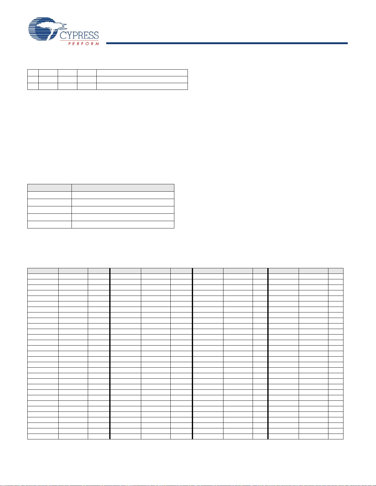
Table 4. 48-Pin Part Pinout (QFN**)
46 IO I P0[1] Analog column mux input.
47 IO P2[7]
48 IO P2[5]
LEGEND: A = Analog, I = Input, and O = Output.
* These are the ISSP pins, which are not High Z at POR (Power On Reset).
** The QFN package has a center pad that must be connected to ground (Vss).
Register Reference
CY8CLED16
Register Conventions
Abbreviations Used
The register conventions specific to this section are listed in the
following table.
Register Mapping Tables
This chapter lists the registers of the CY8CLED16 EZ-Color
device.
The device has a total register address space of 512 bytes. The
register space is referred to as IO space and is divided into two
banks. The XOI bit in the Flag register (CPU_F) determines
Convention Description
R Read register or bit(s)
W Write register or bit(s)
L Logical register or bit(s)
C Clearable register or bit(s)
# Access is bit specific
which bank the user is currently in. When the XOI bit is set the
user is in Bank 1.
Note In the following register mapping tables, blank fields are
reserved and should not be accessed.
Table 5. Register Map Bank 0 Table: User Space
Name Addr (0,Hex) Access Name Addr (0,Hex) Access Name Addr (0,Hex)
PRT0DR 00 RW DBB20DR0 40 # ASC10CR0 80 RW RDI2RI C0 RW
PRT0IE 01 RW DBB20DR1 41 W ASC10CR1 81 RW RDI2SYN C1 RW
PRT0GS 02 RW DBB20DR2 42 RW ASC10CR2 82 RW RDI2IS C2 RW
PRT0DM2 03 RW DBB20CR0 43 # ASC10CR3 83 RW RDI2LT0 C3 RW
PRT1DR 04 RW DBB21DR0 44 # ASD11CR0 84 RW RDI2LT1 C4 RW
PRT1IE 05 RW DBB21DR1 45 W ASD11CR1 85 RW RDI2RO0 C5 RW
PRT1GS 06 RW DBB21DR2 46 RW ASD11CR2 86 RW RDI2RO1 C6 RW
PRT1DM2 07 RW DBB21CR0 47 # ASD11CR3 87 RW C7
PRT2DR 08 RW DCB22DR0 48 # ASC12CR0 88 RW RDI3RI C8 RW
PRT2IE 09 RW DCB22DR1 49 W ASC12CR1 89 RW RDI3SYN C9 RW
PRT2GS 0A RW DCB22DR2 4A RW ASC12CR2 8A RW RDI3IS CA RW
PRT2DM2 0B RW DCB22CR0 4B # ASC12CR3 8B RW RDI3LT0 CB RW
PRT3DR 0C RW DCB23DR0 4C # ASD13CR0 8C RW RDI3LT1 CC RW
PRT3IE 0D RW DCB23DR1 4D W ASD13CR1 8D RW RDI3RO0 CD RW
PRT3GS 0E RW DCB23DR2 4E RW ASD13CR2 8E RW RDI3RO1 CE RW
PRT3DM2 0F RW DCB23CR0 4F # ASD13CR3 8F RW CF
PRT4DR 10 RW DBB30DR0 50 # ASD20CR0 90 RW CUR_PP D0 RW
PRT4IE 11 RW DBB30DR1 51 W ASD20CR1 91 RW STK_PP D1 RW
PRT4GS 12 RW DBB30DR2 52 RW ASD20CR2 92 RW D2
PRT4DM2 13 RW DBB30CR0 53 # ASD20CR3 93 RW IDX_PP D3 RW
PRT5DR 14 RW DBB31DR0 54 # ASC21CR0 94 RW MVR_PP D4 RW
PRT5IE 15 RW DBB31DR1 55 W ASC21CR1 95 RW MVW_PP D5 RW
PRT5GS 16 RW DBB31DR2 56 RW ASC21CR2 96 RW I2C_CFG D6 RW
PRT5DM2 17 RW DBB31CR0 57 # ASC21CR3 97 RW I2C_SCR D7 #
PRT6DR 18 RW DCB32DR0 58 # ASD22CR0 98 RW I2C_DR D8 RW
PRT6IE 19 RW DCB32DR1 59 W ASD22CR1 99 RW I2C_MSCR D9 #
PRT6GS 1A RW DCB32DR2 5A RW ASD22CR2 9A RW INT_CLR0 DA RW
PRT6DM2 1B RW DCB32CR0 5B # ASD22CR3 9B RW INT_CLR1 DB RW
PRT7DR 1C RW DCB33DR0 5C # ASC23CR0 9C RW INT_CLR2 DC RW
PRT7IE 1D RW DCB33DR1 5D W ASC23CR1 9D RW INT_CLR3 DD RW
Blank fields are Reserved and should not be accessed. # Access is bit specific.
Acces
Name Addr (0,Hex)
Acces
Document Number: 001-13105 Rev. ** Page 12 of 39
 Loading...