

Page 1

PSoC
CY8CKIT-001
®
Development Kit Guide
Doc. # 001-48651 Rev. *J
May 3, 2012
Cypress Semiconductor
198 Champion Court
San Jose, CA 95134-1709
Phone (USA): 800.858.1810
Phone (Intnl): 408.943.2600
http://www.cypress.com
Page 2

Copyrights
Copyrights
© Cypress Semiconductor Corporation, 2009-2012. The inform ation contained herein is subject to change without notice.
Cypress Semiconductor Corporation assumes no responsib ility for the use of any circu itry other than circuitry embodied in a
Cypress product. Nor does it convey or imply any license under patent or other rights. Cypress products are not warranted
nor intended to be used for medical, life support, life saving, critical control o r safety applications, unless pursuant to an
express written agreement with Cypress. Furthermore, Cypress does not authorize its products for use as critical components
in life-support systems where a malfunction or failure may reasonably be expected to result in significant injury to the user.
The inclusion of Cypress products in life-support systems application implies that the manufacturer assumes all risk of such
use and in doing so indemnifies Cypress against all charges.
Any Source Code (software and/or firmware) is owned by Cypress Semiconductor Corporation (Cypress) and is protected by
and subject to worldwide patent protection (United States and foreign), United States copyright laws and international treaty
provisions. Cypress hereby grants to licensee a personal, non-exclusive, non-transferable license to copy, use, modify, create
derivative works of, and compile the Cypress Source Code and derivative works for the sole purpose of creating custom software and or firmware in support of licensee product to be used only in conjunction with a Cypress integrated circuit as specified in the applicable agreement. Any reproduction, modification, transla tion, compilation, or representation of this Source
Code except as specified above is prohibited without the express written permission of Cypress.
Disclaimer: CYPRESS MAKES NO WARRANTY OF ANY KIND, EXPRESS OR IMPLIED, WITH REGARD TO THIS MATERIAL, INCLUDING, BUT NOT LIMITED TO, THE IMPLIED WARRANTIES OF MERCHANTABILITY AND FITNESS FOR A
PARTICULAR PURPOSE. Cypress reserves the right to make changes without further notice to the materials described
herein. Cypress does not assume any liability arising out of the applica tion or use of any product or circuit described herein.
Cypress does not authorize its products for use as critical components in life-support systems whe re a malfunction or failure
may reasonably be expected to result in significant injury to the user. The inclusion of Cypress’ product in a life-support systems application implies that the manufacturer assumes all risk of such use and in doing so indemnifies Cypress against all
charges.
Use may be limited by and subject to the applicable Cypress software license agreement.
PSoC Designer™ and PSoC Creator™ are trademarks and PSoC® and CapSense® are registered trademark of Cypress
Semiconductor Corp. All other trademarks or registered trademarks referenced herein are property of the respective corporations.
Flash Code Protection
Cypress products meet the specifications contained in their particular Cypress PSoC Datasheets. Cypress believes that its
family of PSoC products is one of the most secure families of its kind on the market today, regardless of how they are used.
There may be methods, unknown to Cypress, that can breach the code protecti on features. Any of these methods, to our
knowledge, would be dishonest and possibly illegal. Neither Cypress nor any other semiconductor manufacturer can guarantee the security of their code. Code protection does not mean that we are guaranteeing the prod uct as "unbreakable."
Cypress is willing to work with the customer who is concerned about the inte grity of their code. Co de prot ection i s constantly
evolving. We at Cypress are committed to continuously improving the code protection features of our products.
2 CY8CKIT-001 PSoC Development Kit Guide, Doc. # 001-48651 Rev. *J
Page 3

Contents
1. Introduction 7
1.1 Kit Overview........... ... ... ... .... ...................................... .... ... ... ....................................... ..7
1.2 Kit Contents..................................... ... ... ....................................... ... ... .........................7
1.3 Installation....................................................................................................................8
1.4 PSoC Development Board.........................................................................................10
1.5 Kit Revision............... ... ... .... ... ... ... .... ...................................... .... ... .............................12
1.6 Additional Resources................ ... ....................................... ... .... ... ... ... ... .... ... ... ..........13
1.7 Document Conventions .............................................................................................13
1.8 Document Revision History ......................................................................................14
1.3.1 Before You Begin .............................................................................................8
1.3.2 Prerequisites....................................................................................................8
1.3.3 Installing PSoC 1 Development Software...................................................... ..8
1.3.4 Installing PSoC 3 Development Software...................................................... ..8
1.3.5 Installing PSoC 5 Development Software...................................................... ..9
1.4.1 Default Switch and Jumper Settings ..............................................................10
1.6.1 Beginner Resources.......................................................................................13
1.6.2 Engineers Looking for More...........................................................................13
1.6.3 Learning from Peers.......................................................................................13
2. Loading My First PSoC Project 15
2.1 My First PSoC 1 (CY8C28) Project .............................. ... ... ... .... ... ... ..........................16
2.1.1 Loading My First PSoC 1 Project...................................................................16
2.1.2 Building My First PSoC 1 Project................................................................... 17
2.1.3 Programming My First PSoC 1 Project ..........................................................17
2.1.4 Running My First PSoC 1 Project ..................................................................18
2.2 My First PSoC 1 (CY8C29) Project .............................. ... ... ... .... ... ... ..........................20
2.2.1 Loading My First PSoC 1 Project...................................................................20
2.2.2 Building My First PSoC 1 Project................................................................... 21
2.2.3 Programming My First PSoC 1 Project ..........................................................22
2.2.4 Running My First PSoC 1 Project ..................................................................23
2.3 My First PSoC 3 (CY8C38) Project .............................. ... ... ... .... ... ... ..........................25
2.3.1 Loading My First PSoC 3 Project...................................................................25
2.3.2 Building My First PSoC 3 Project................................................................... 26
2.3.3 Programming My First PSoC 3 Project ..........................................................27
2.3.4 Running My First PSoC 3 Project ..................................................................28
2.4 My First PSoC 5 (CY8C55) Project .............................. ... ... ... .... ... ... ..........................28
2.4.1 Loading my First PSoC 5 Project...................................................................28
2.4.2 Building My First PSoC 5 Project................................................................... 30
2.4.3 Programming My First PSoC 5 Project ..........................................................31
2.4.4 Running My First PSoC 5 Project ..................................................................32
CY8CKIT-001 PSoC Development Kit Guide, Doc. # 001-48651 Rev. *J 3
Page 4

Contents
3. Sample Projects 33
3.1 CY8C28 Family Processor Module Code Examples.................................................33
3.1.1 My First PSoC 1 (CY8C28) Project................................................................33
3.1.2 ADC to LCD Project.......................................................................................41
3.1.3 ADC to UART with DAC.................................................................................48
3.1.4 CapSense......................................................................................................60
3.2 CY8C29 Family Processor Module Code Examples.................................................70
3.2.1 My First PSoC 1 (CY8C29) Project................................................................70
3.2.2 ADC to LCD Project.......................................................................................78
3.2.3 ADC to LCD with DAC and UART .................................................................85
3.3 CY8C38 / CY8C55 Family Processor Module Code Examples ..............................102
3.3.1 My First PSoC 3 / PSoC 5 Project ...............................................................102
3.3.2 ADC to LCD Project..................................................................................... 111
3.3.3 ADC to UART with DAC............................................................................... 118
3.3.4 USB HID .............................................................. ....................................... .135
3.3.5 CapSense....................................................................................................149
3.3.6 SAR ADC (PSoC 5 Only).. ... ... ... .... ... ....................................... ... ... ... ... .... ....158
Appendix A. Board Specifications and Layout 175
A.1 PSoC Development Board ......................................................................................175
A.1.1 Factory Default Configuration.............. ... .... ... ... ... ... .... ... ... ... .... ....................175
A.1.2 Power Supply Configuration Examples........................................................176
A.1.3 Prototyping Components ........................ .... ... ... ... ... .... ... ... ... .... ... ... ... ...........181
A.1.4 LCD Module.................................................................................................183
A.1.5 CapSense Elements....................................................................................184
A.1.6 Processor Module........................................................................................184
A.1.7 Expansion Ports...........................................................................................188
A.2 Schematics..............................................................................................................191
A.2.1 CY8CKIT-001 PSoC Development Board ...................................................191
A.2.2 CY8C28 Family Processor Module..............................................................192
A.2.3 CY8C29 Family Processor Module..............................................................193
A.2.4 CY8C38 Family Processor Module..............................................................194
A.2.5 CY8C55 Family Processor Module..............................................................195
A.2.6 Enabling Boost Component in PSoC 3 and PSoC 5 Processor Modules....196
A.3 Bill of Materials........................................................................................................196
A.3.1 CY8CKIT-001 PSoC Development Board ...................................................196
A.3.2 CY8C28 Family Processor Module..............................................................198
A.3.3 CY8C29 Family Processor Module..............................................................198
A.3.4 CY8C38 Family Processor Module..............................................................199
A.3.5 CY8C55 Family Processor Module..............................................................200
Appendix B. MiniProg3 203
B.1 MiniProg3 LEDs.......................................................................................................203
B.2 Programming in Power Cycle Mode........................................................................203
B.3 Interface Pin Assignment Table...............................................................................203
B.4 Protection Circuitry..................................................................................................204
B.5 Level Translation.....................................................................................................204
Appendix C. MiniProg3 Technical Description 205
C.1 Interfaces.................................................................................................................206
C.1.1 ISSP.............................................................................................................206
C.1.2 JTAG............................................................................................................206
4 CY8CKIT-001 PSoC Development Kit Guide, Doc. # 001-48651 Rev. *J
Page 5

Contents
C.1.3 SWD/SWV....................................................................................................206
C.1.4 I2C™............................................................................................................206
C.2 Connectors ..............................................................................................................207
C.2.1 5-Pin Connector...........................................................................................207
C.2.2 10-Pin Connector.................................... ... ... .... ... ....................................... .207
C.3 Power.......................................................................................................................209
CY8CKIT-001 PSoC Development Kit Guide, Doc. # 001-48651 Rev. *J 5
Page 6

Contents
6 CY8CKIT-001 PSoC Development Kit Guide, Doc. # 001-48651 Rev. *J
Page 7

1. Introduction
1.1 Kit Overview
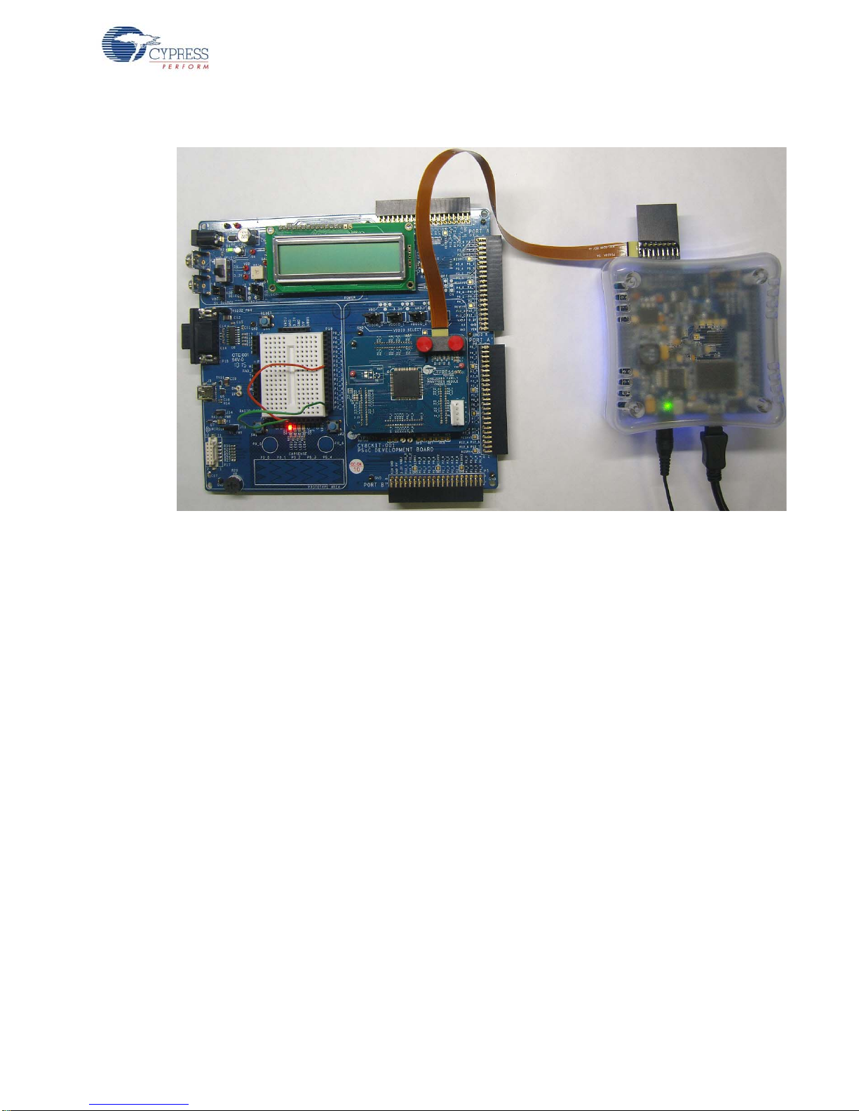
The CY8CKIT-001 PSoC® Development Kit provides a common development platform where you
can prototype and evaluate different solutions using either the PSoC 1, PSoC 3, or PSoC 5
architectures. This guide gives you a practical understanding of PSoC technology. The kit also
includes several code examples with step-by-step instructions to enable you to ea sily d evelop PSoC
solutions. This kit includes PSoC CY8C28, CY8C38, and CY8C55 family processor modules.
1.2 Kit Contents
The CY8CKIT-001 PSoC Development Kit includes:
■ PSoC development board
■ PSoC CY8C28 family processor module
■ PSoC CY8C38 family processor module
■ PSoC CY8C55 family processor module
■ MiniProg3 programmer and debug tool
■ USB cable
■ 12-V power supply adapter
■ Wire pack
■ Printed documentation
❐ Quick start guide
❐ Schematic and pinout of PSoC development board design
■ PSoC 1 software CD/DVD (contents are installed in \PSoC Development Kit CY8C28):
❐ PSoC Designer™ IDE
❐ PSoC Programmer software
❐ CY8C28 datasheets
❐ Kit release notes
❐ Software release notes
❐ Code example files, firmware, and documentation
■ PSoC 3 and PSoC 5 software CD/DVD (contents are installed in the \CY8CKIT-009A folder for
PSoC 3 module kit and \PSoC Development Kit CY8C55 folder for PSoC 5 module kit):
❐ PSoC Creator™ IDE
❐ PSoC Programmer software
❐ CY8C38 datasheet
❐ CY8C55 datasheet
❐ Kit release notes
❐ Software release notes
❐ Code example files, firmware, and documentation
1
1. Any USB certified cable up to 2 meters in length can be used with the DVK.
CY8CKIT-001 PSoC Development Kit Guide, Doc. # 001-48651 Rev. *J 7
Page 8

Introduction
1.3 Installation
Everything you need to use the PSoC Development Kit is included; you only need to install the software for the processor module you plan to use.
Note CY8CKIT-008 CY8C 29 family processor module is not part of this kit; you can purchase this
module from http://www.cypress.com.
1.3.1 Before You Begin
All Cypress software installations require administrator privileges, but this is not required to run the
installed software.
Shut down any currently running Cypress software.
Disconnect any ICE-Cube or MiniProg devices from your computer.
1.3.2 Prerequisites
PSoC Creator and PSoC Designer both use Microsoft .NET Framework, Adobe Acrobat Reader,
and a Windows Installer. If .NET Framework and Windows Installer are not on your computer, the
installation automatically installs them. If you do not have Adobe Acrobat Reader, download and
install it from the Adobe website.
1.3.3 Installing PSoC 1 Development Software
To use the CY8C28 or CY8C29 family processor module (PSoC 1), you need:
■ PSoC Designer 5.0 SP6 or higher
■ PSoC Programmer 3.12.3 or later
If PSoC Designer 5.0 is currently installed, uninstall it. Click Start Control Panel Add or
Remove Programs.
Insert the PSoC 1 Software CD/DVD; using the menu, select Install Software for PSoC 1.
After installation, user guides and key documents are located in the \Documentation subdirectory
of the PSoC Designer installation directory.
1.3.4 Installing PSoC 3 Development Software
To use the CY8C38 family processor module (PSoC 3), you need:
■ PSoC Creator 1.0 Production or later
■ PSoC Programmer 3.12.3 or later
■ PSoC Development Kit example files
Insert the PSoC 3 or PSoC 5 software CD/DVD; in the menu, select Install Software for PSoC 3.
This option installs all three required software packages. The installers for PSoC Programmer and
PSoC Creator automatically start before the kit examples are installed.
For each installation, select Typical on the Installation Type page.
PSoC Creator uses the DP8051 Keil 8.16 compiler to build PSoC 3 applications. This compiler is
included on the CD/DVD; if the installer does not detect the compiler, you w ill be prompted to install
it.
Note The Keil compiler is distributed with a free license. You must activate this license within 30
days of installation. When the Cypress soft ware installation is complete, and you run PSoC Creator,
activate the compiler license from Help
8 CY8CKIT-001 PSoC Development Kit Guide, Doc. # 001-48651 Rev. *J
Register Keil.
Page 9

Introduction
Important for Win7 and Vista users: Rename the *_tools.ini file in <Install_Directory>:\
PSoC Creator\<version>\PSoC Creator\import\keil\pk51\<version> to "tools.ini" for
the Keil registration to be successful.
After installing PSoC Creator and PSoC Programmer, refer to the documentation as needed:
■ PSoC Creator Help Topics Getting Started
■ Programmer Documentation User Guide
Other documents included with this release are located in the \Documentation subdirectory of the
PSoC Creator installation directory. The default location is:
<Install_Directory>:\PSoC Creator\<version>\PSoC Creator\Documentation
You can access this directory from within PSoC Creator under Help
include (but are not limited to):
■ PSoC Creator Component Author Guide (component_author_guide.pdf)
■ Warp Verilog Reference Guide (warp_verilog_reference.pdf)
■ Customization API Reference (customizer_api.chm)
Note After the installation is complete, the kit contents are available at the following location:
<Install_Directory>:\CY8CKIT-009A\<version>
1.3.5 Installing PSoC 5 Development Software
To use the CY8C55 family processor module (PSoC 5), you need:
■ PSoC Creator 2.0 or later
■ PSoC Programmer 3.12.3 or later
■ PSoC Development Kit example files
Insert the PSoC 3 or PSoC 5 Software CD/DVD; in the menu, select Install Software for PSoC 5.
This option installs all three required software packages. The installers for PSoC Programmer and
PSoC Creator automatically start before the kit examples are installed.
For each installation, select Typical on the Installation Type page.
PSoC Creator uses the GNU GCC 4.4.1 compiler to build PSoC 5 applications.
After installing PSoC Creator and PSoC Programmer, refer to the documentation as needed:
■ PSoC Creator Help Topics Getting Started
■ Programmer Documentation User Guide
Documentation. Documents
Other documents included with this release are located in the \Documentation subdirectory of the
PSoC Creator installation directory. The default location is:
<Install_Directory>:\PSoC Creator\<version>\PSoC Creator\Documentation
You can access this directory from within PSoC Creator under Help
include (but are not limited to):
■ PSoC Creator Component Author Guide (component_author_guide.pdf)
■ Warp Verilog Reference Guide (warp_verilog_reference.pdf)
■ Customization API Reference (customizer_api.chm)
Note After the installation is complete, the kit contents are available at the following location:
<Install_Directory>:\PSoC Development Kit CY8C55\<version>
CY8CKIT-001 PSoC Development Kit Guide, Doc. # 001-48651 Rev. *J 9
Documentation. Documents
Page 10

Introduction
1.4 PSoC Development Board
The CY8CKIT-001 PSoC Development Board is designed to aid hardware, firmware, and software
developers in building their own systems around Cypress’s PSoC devices. The flexibility to configure
the power domains is one of the foremost features of this board. Input power to the board is from one
of two sources:
■ 12 V 1-A power supply adapter
■ 9-V alkaline battery (not included)
This full-featured board incorporates three onboard linear regulators that power peripherals and
PSoC processor modules at voltages between 1 .7 V and 5.0 V. Th es e r eg ula tors include a fixed 5 V
1-A linear regulator, a fixed 3.3 V 300-mA linear regulator, and a 1.5 V to 3.3 V for 3.3-V supp ly and
1.5 V to 5 V for 5-V supply adjustable regulator. The board also provides the ability to separate the
PSoC core VDD rail into two separate rails, analog and digital. In addition, the board is able to
separate the I/O VDD rails, giving the flexibility to power the I/O ports at different voltages.
The board is equipped with a 2×16 alphanumeric LCD module capable of 1.8 V to 5.0 V I/O. In
addition, there is a mini-B full-speed USB interface and a female DB9 serial communications
interface. Also included is a 12-pin wireless radio module interface, which can be used to develop
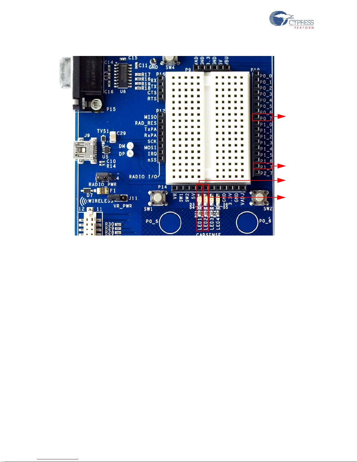
CyFi™ low-power RF or other embedded RF solutions with this kit. The board also has a prototypin g
area containing a small breadboard, complete with I/O port sockets nearby, multipurpose LEDs,
mechanical push buttons, and a multipurpose variable resis tor. In addition, three capacitive sensing
elements (two buttons and a five seg ment slider) are included o n the boar d to allow the evalu ation of
CapSense
®
applications.
The board has four general-purpose I/O (GPIO) e xpansion slots, allowing the I/O to expand to external boards.
The board is designed with modularity in mind and, as a result, supports removable processor modules. This allows you to plug different PSoC processor modules into the board based upon the
desired features of both 8-bit and 32-bit PSoC devices.
Note
■ The PSoC device may get hot or damaged if many I/O pins are configured as strong drive with
initial state HIGH and grounded externally using wires.
■ The PSoC device may get hot or damaged if many I/O pins are configured as strong drive with
initial state LOW and connected to Vcc externally using wire s.
1.4.1 Default Switch and Jumper Settings
Jumpers on the CY8CKIT-001 PSoC development board have a default setting to operate at 3.3 V.
For default configuration, each of the jumpers must be set according to these instructions.
Note All CY8C28 and CY8C29 family processor module code examples are configured for 5 V . Configure the board to 5 V, before creating the code examples.
SW3 - VDD Select. Default Position: 3.3 V (down position)
10 CY8CKIT-001 PSoC Development Kit Guide, Doc. # 001-48651 Rev. *J
Page 11
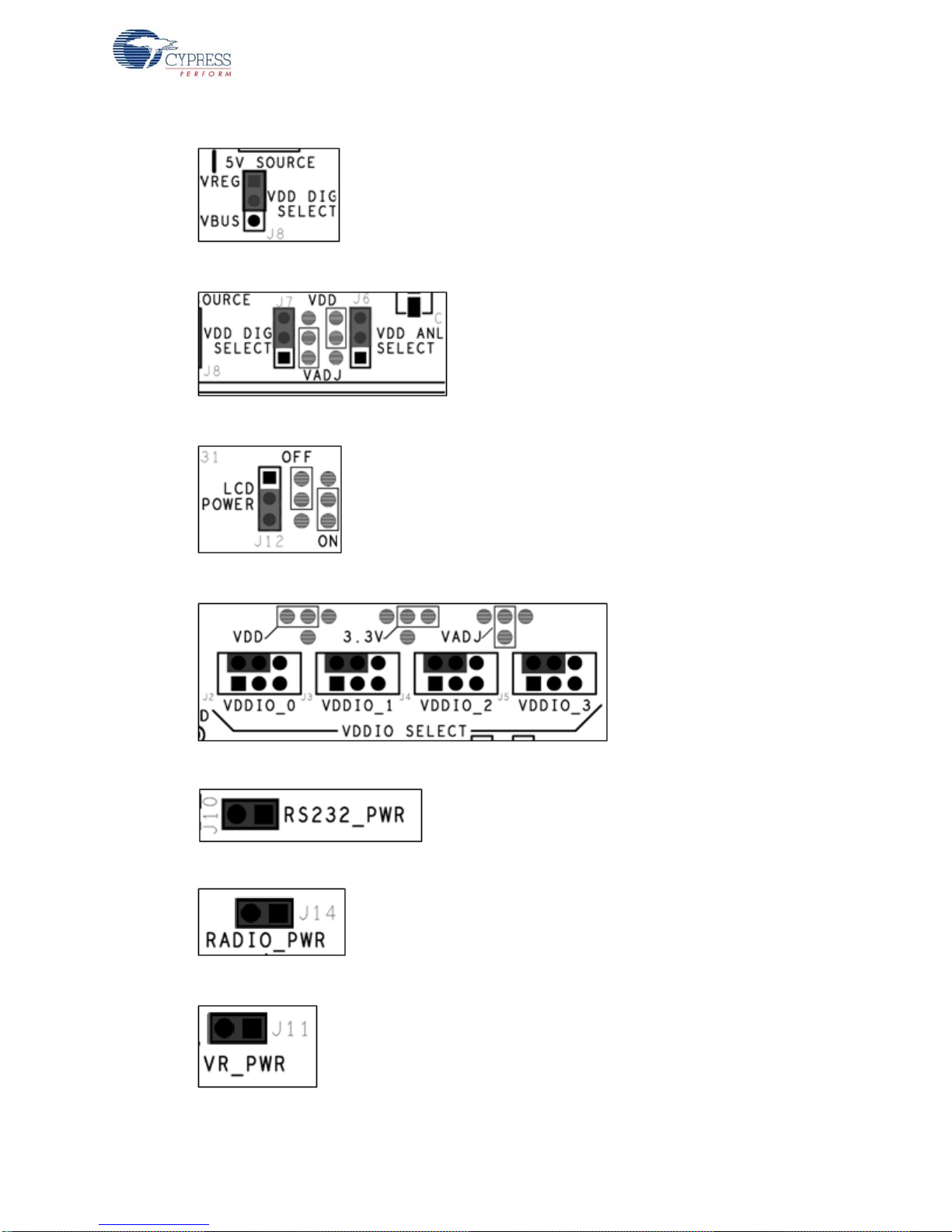
J8 - 5 V Source. Default Position: VREG (upper two pins)
J7, J6 - VDD Digital, VDD Analog. Default Position: VDD (upper two pins, both headers)
J12 - LCD Power. Default Position: ON (lower two pins)
Introduction
J2-J5 - VDDIO Power Select. Default Position: VDD (upper left two pins)
J10 - RS-232 Power (Serial Communications). Default Position: Installed
J14 - Radio Power. Default Position: Installed
J11 - Variable Resistor Power. Default Position: Installed
CY8CKIT-001 PSoC Development Kit Guide, Doc. # 001-48651 Rev. *J 11
Page 12

Introduction
1.4.1.1 AC/DC Adaptor Specifications
Use adaptors with the following specifications:
■ Input voltage: 100 to 240 VAC, 50 Hz to 60 Hz, 1 A
■ Output voltage: 12 VDC, 1 A
■ Power output: 12 W
■ Polarization: Positive center
■ Certification: CE certified
Some recommended part numbers include EPSA120100U-P5P-EJ (CUI Inc.) and LTE12W-S2 (Li
Tone Electronics Co. Ltd).
1.4.1.2 Battery Specifications
Use batteries with the following specifications:
■ Battery type: 9 V
■ Output voltage: 9 VDC
■ Type: Non-rechargeable alkaline consumer batteries
■ RoHS status: RoHS compliant
■ Lead free status: Pb-free
Some recommended part numbers include 6LR61XWA/1SB (Panasonic), MN1604 (Duracell), and
6LR61 (Energizer).
1.5 Kit Revision
To know the kit revision, look for the white sticker on the bottom left on the back of the kit box. If the
revision reads CY8CKIT-001B Rev **, then congratulations, you own the latest version.
You can also check the silicon marketing part number on the processor module. If the part number is
CY8C3866AXI-040, then congratulations, you own the latest version.
To upgrade CY8CKIT-001A to CY8CKIT-001B, the PSoC 3 proc esso r mod ule and kit CD/DVD m ust
be updated. Purchase the latest pro ces sor mo dule at http://www.cypress.com/go/CY8CKIT-009 and
download the latest CD ISO image at http://www.cypress.com/go/CY8CKIT-001.
To upgrade CY8CKIT-001 to CY8CKIT-001B, besides the upgrades stated above, you need to purchase the latest PSoC 5 process module at http://www.cypress.com/go/CY8CKIT-010.
12 CY8CKIT-001 PSoC Development Kit Guide, Doc. # 001-48651 Rev. *J
Page 13

1.6 Additional Resources
Visit http://www.cypress.com/go/training for additional learning resources in the form of datasheets,
technical reference manual, and application notes.
1.6.1 Beginner Resources
AN54181 - PSoC 3 - Getting Started with a PSoC 3 Design Project
PSoC Designer Training
PSoC Designer FAQ
PSoC Creator Training
1.6.2 Engineers Looking for More
AN54460 - PSoC 3 and PSoC 5 Interrupts
AN52705 - PSoC 3 and PSoC 5 - Getting Started with DMA
AN52701 - PSoC 3 - How to Enable CAN Bus Communication
AN54439 - PSoC 3 and PSoC 5 External Oscillator
Introduction
AN52927 - PSoC 3: Segment LCD Direct Drive
Cypress continually strives to provide the best support. Click here to view a growing list of
application notes for PSoC 3 and PSoC 5.
1.6.3 Learning from Peers
Cypress Developer Community Forums
1.7 Document Conventions
These conventions are used throughout this guide.
Table 1-1. Documentation Conventions
Convention Usage
Courier New
Size 12
Italics Displays file names and reference documentation:
[bracketed, bold] Displays keyboard commands in procedures:
Bold With Arrows Represents menu paths, user entered text:
Bold Displays commands and selections, and icon names in procedures:
Note Displays functionality unique to PSoC Designer, PSoC Creator, or the PSoC
WARNING: Displays cautions that are important to the subject.
Displays file locations and source code:
C:\ …cd\icc\.
sourcefile.hex
[Enter] or [Ctrl] [C]
File New Project Clone
Click the Debugger icon, and then click Next.
device.
CY8CKIT-001 PSoC Development Kit Guide, Doc. # 001-48651 Rev. *J 13
Page 14

Introduction
1.8 Document Revision History
Document Title: CY8CKIT-001 PSoC Development Kit Guide
Document Number: 001-48651
Revision Issue Date
** 6/23/09 AESA New Guide
*A 7/22/09 AESA CDT based updates
*B 1 1/19/09 AESA CDT based updates
*C 05/21/10 AESA Updated with PSoC 5.
*D 01/05/11 RKAD
*E 02/10/11 RKAD Updated images. Added Kit Revi sion section
*F 12/16/11 RKAD Content updates throughout the document.
*G 12/30/11 RKAD
*H 01/13/12 RKAD
*I 01/18/12 RKAD
*J 05/03/12 SASH Added the Additional Resources section
Origin of
Change
Updated images. Updated PSoC Creator and PSoC Programmer
versions
Updated installation directory path. Added Figure 2-4 and Figure 2-
10. Added note on Keil compilers in section 1.3.4.
Added note on USB cable in section 1.2 - Kit Contents. Appended
to note in section A.1.4 - LCD Module
Minor ECN to include attachments in pdf. No content updates
made.
Description of Change
14 CY8CKIT-001 PSoC Development Kit Guide, Doc. # 001-48651 Rev. *J
Page 15

2. Loading My First PSoC Project
The CY8CKIT-001 PSoC Development Kit supports projects across the PSoC 1, PSoC 3, and
PSoC 5 architectures. This section walks you through the high-level design process for opening,
building, programming, and running your first PSoC project using this kit.
Before beginning, follow each of these steps to make certain that your software and hardware
environments are properly configured and ready for these projects:
1. Install PSoC Designer using the steps listed in Installing PSoC 1 Development Software on
page 8.
2. Install PSoC Creator using the steps listed in Installing PSoC 3 Development Software on page 8.
3. Connect the MiniProg3 into your PC using the supplied USB cable. When you connect the
MiniProg3, Microsoft Windows
are installed as part of the PSoC Programmer installation process; however, if Windows opens
the driver installation dialog boxes, accept the defaults and allow Win dows to automatically find
the appropriate driver.
4. Close any open PSoC Creator or PSoC Designer applications and projects.
5. Configure the PSoC development board (jumper settings and switches) in its default configuration, as described in Default Switch and Jumper Settings on page 10.
6. Use the PSoC CY8C28 family processor module or PSoC CY8C29 family processor module for
the PSoC 1 version of your first PSoC project (My First PSoC 1 (CY8C28) Project on page 16 or
My First PSoC 1 (CY8C29) Project on page 20).
7. Use the PSoC CY8C38 family processor module for the PSoC 3 version of your first PSoC
project (My First PSoC 3 (CY8C38) Project on page 25).
8. Use the PSoC CY8C55 family processor module for the PSoC 5 version of your first PSoC
project (My First PSoC 5 (CY8C55) Project on page 28).
9. For a PSoC 1 project, use the ISSP header on the PSoC CY8C28 family processor module or
PSoC CY8C29 family processor module and connect the MiniProg3 ISSP port.
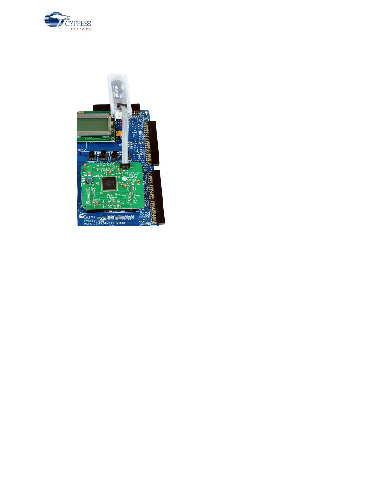
10.For a PSoC 3 or PSoC 5 project, use the JTAG ribbon cable. Connect the ribb on cable to the
MiniProg3 and the CY8C38 family processor module or CY8C55 family processor module into
the header labeled PROG on the processor module.
Note The MiniProg3 should not be "hot plugged" into processor modules that are attached to the
PSoC development board. In other words, do not plug the ribbon cable of the MiniProg3 into the
processor module while code is actively running on the module. Doing so may cause the PSoC
device to unintentionally reset. Power down the PSoC development board and module by
unplugging the power supply from the development board before att aching the MiniProg3 device
to the module board. When the ribbon cable is attached to the module board, power the system
by plugging in the power supply to the PSoC development board. This will avoid any undesirable
PSoC device resets.
11.Power the PSoC development board using the 12-V AC power supply adapter.
®
may indicate that it has found new hardware. All required drivers
CY8CKIT-001 PSoC Development Kit Guide, Doc. # 001-48651 Rev. *J 15
Page 16
Loading My First PSoC Project
2.1 My First PSoC 1 (CY8C28) Project
This is a simple PSoC 1 project using a pulse width modulator (PWM) peripheral inside PSoC, and
software to control the blinking rates of two different LED outputs. For this project, be sure you have
the PSoC CY8C28 family processor module inserted into the PSoC development board and the
appropriate software installed. This section walks you through the steps to open, build, and program
a project.
2.1.1 Loading My First PSoC 1 Project
1. Open PSoC Designer.
2. In the Start Page, navigate to File
3. Navigate to the pr oje ct dir ec to ry: <Install_Directory>:\PSoC Developent Kit
CY8C28\<version>\Firmware\CY8C28.
4. Open the folder Ex1_LED_with_PWM.
5. Double-click Ex1_LED_with_PWM.app.
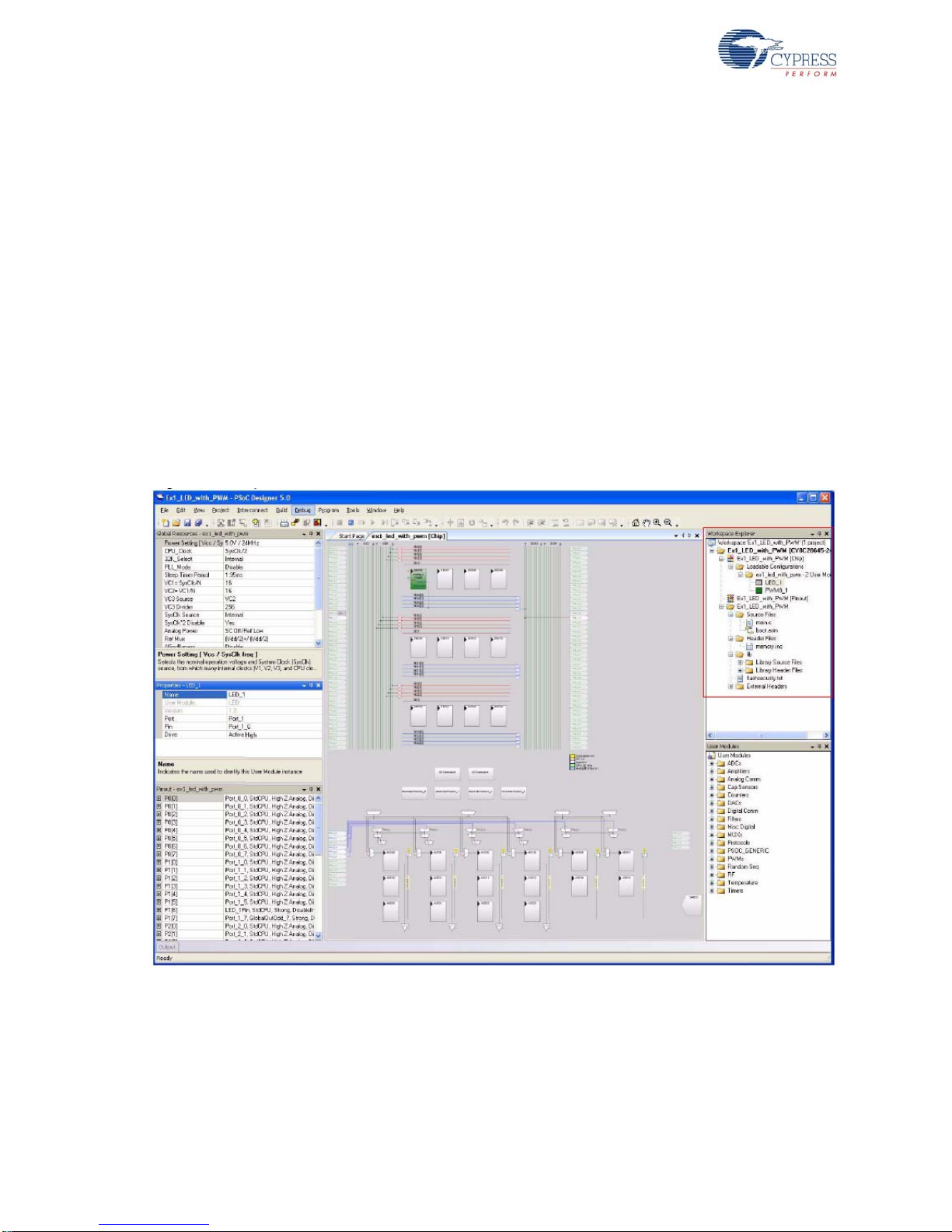
6. The project opens in the Chip Editor view. All project files are in the Workspace Explorer.
Figure 2-1. Chip Editor View
Open Project/Workspace
16 CY8CKIT-001 PSoC Development Kit Guide, Doc. # 001-48651 Rev. *J
Page 17
2.1.2 Building My First PSoC 1 Project
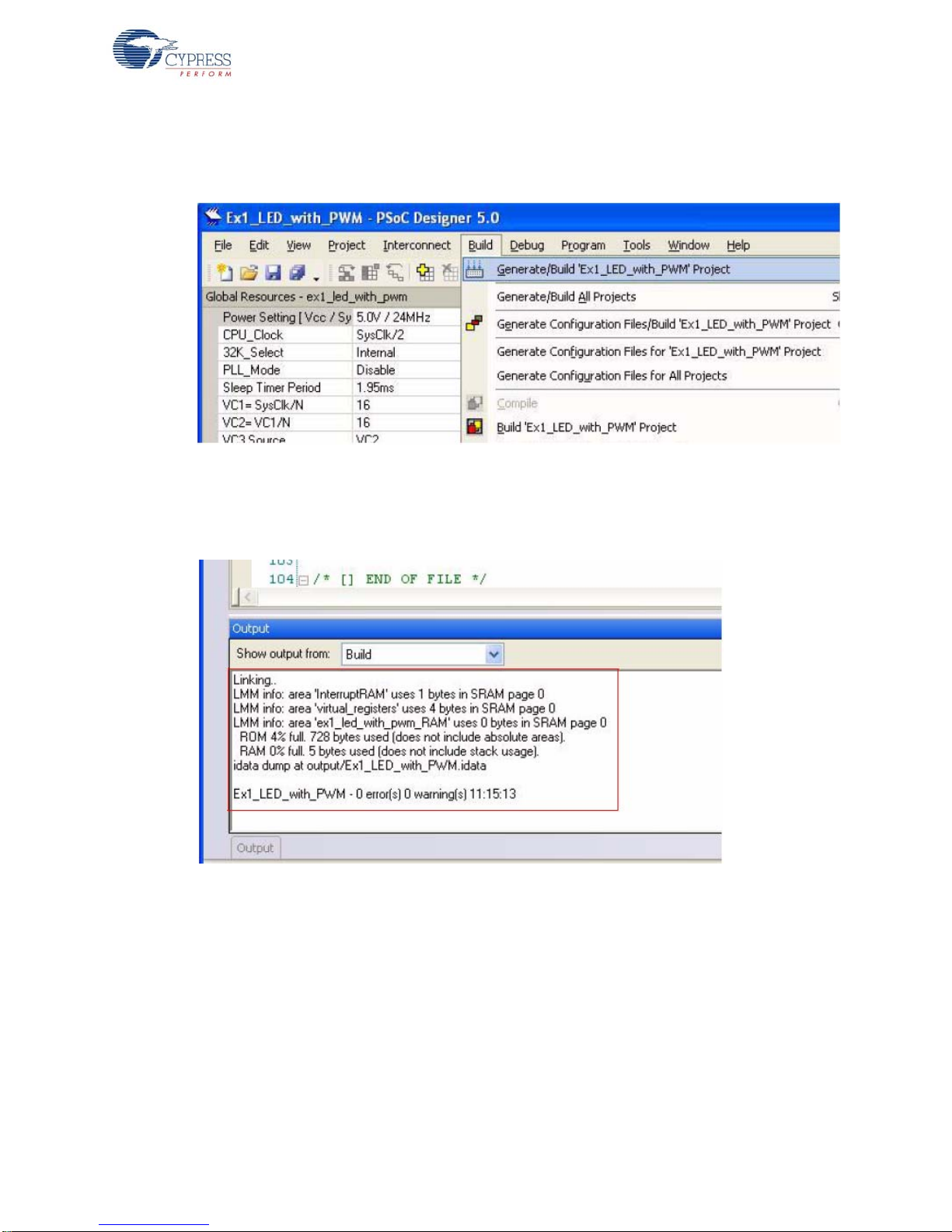
1. Select Build Generate/Build 'Ex1_LED_with_PWM' Project.
Figure 2-2. Build Project
2. PSoC Designer builds the project and displays comments in the Output window. When you see
the message that the project is built with 0 errors and 0 warnings, you are ready to program the
device.
Loading My First PSoC Project
Figure 2-3. Output Window
2.1.3 Programming My First PSoC 1 Project
1. Open Program Part from within PSoC Designer by selecting Program Program Part.
2. In the Program Part window, ensure that MiniProg3 is selected in the Port Selection box.
3. In the Program Part window, set Acquire Mode to Reset.
4. In the Program Part window, set Verification to On. This ensures that downloaded checksum
matches the actual checksum.
5. In PSoC Programmer, set AutoDetection to On to enable the software to automatically detect
and configure for the target device family and device. If PSoC Programmer is properly
configured, AutoDetection reports a device family of 28xxx.
Note Make sure ISSP protocol is selected.
CY8CKIT-001 PSoC Development Kit Guide, Doc. # 001-48651 Rev. *J 17
Page 18
Loading My First PSoC Project
6. In the Program Part window, click the program arrow to program the device.
7. Wait until programming is completed, to continue.
Note For debugging purposes, the CY8C28 family processor module is designed to accommodate
the use of the CY3215-DK In-Circuit Emulator (ICE-Cube). When using the ICE-Cube debugger,
make certain that PSoC Designer is configured so that the ICE-Cube does not provide power to the
processor module. Within the PSoC Designer application, select Project Settings and select
Debugger from the tree. Make sure that External only is selected under the Pod Power Source
section and select Execute Program from the Debug menu to start debugging.
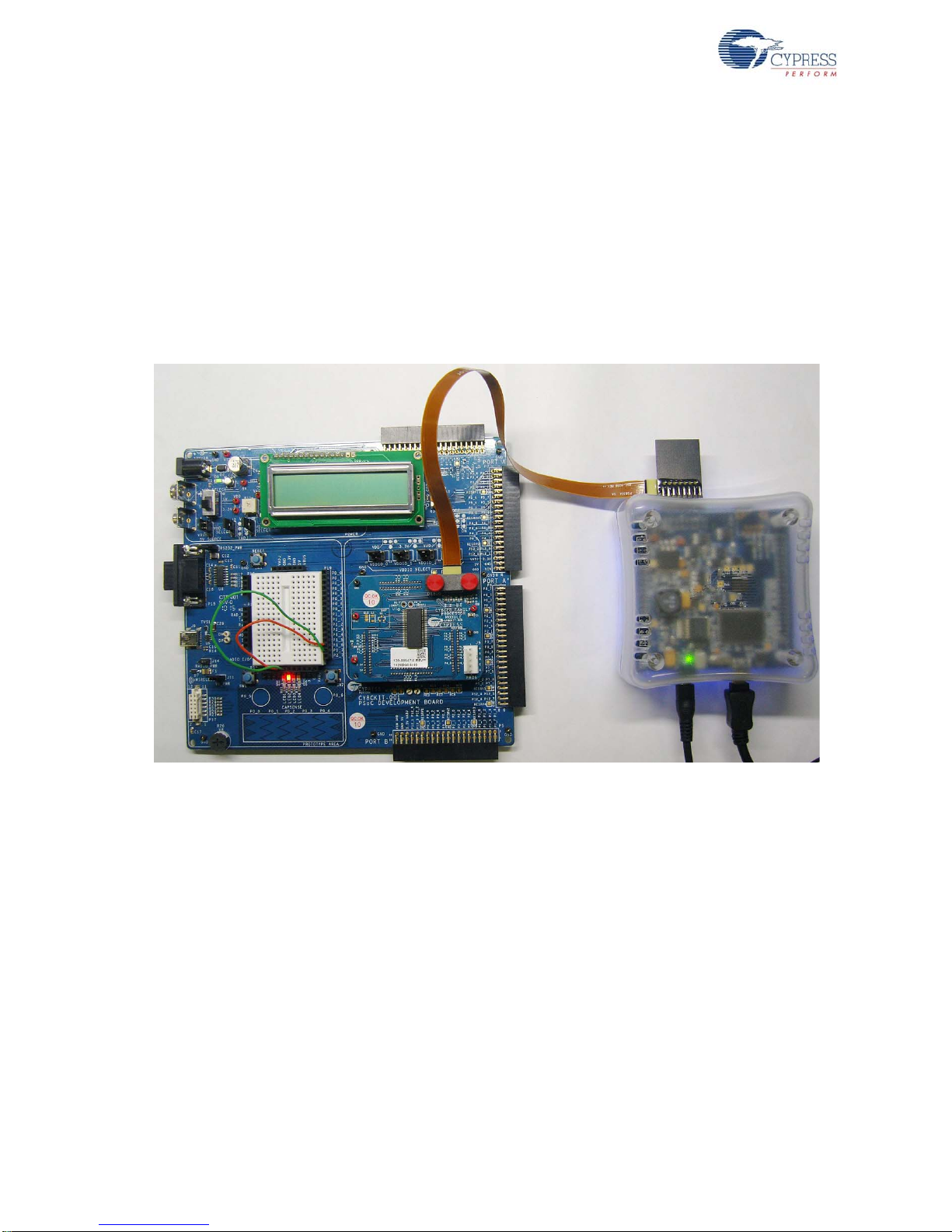
Connect the processor module to the CY3215-DK ICE-Cube, as shown in Figure 2-4.
Figure 2-4. ICE-Cube Connected to CY8C28 (PSoC 1) Processor Module - Debugging the
Ex1_LED_with_PWM Code Example
2.1.4 Running My First PSoC 1 Project
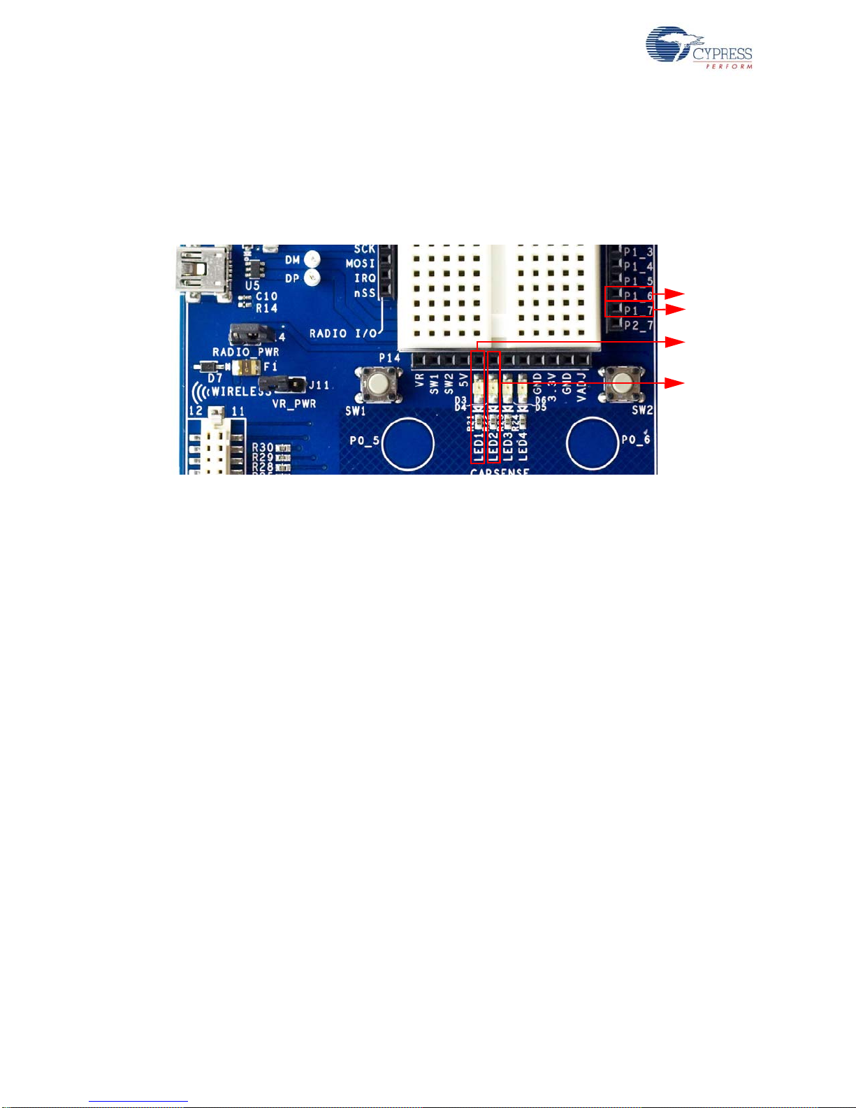
1. Connect P1[6] to LED1 and P1[7] to LED2. Verify that LED1 and LED2 are blinkin g base d on the
project's use of the PWM and software. Now that the PSoC 1 device is programmed, reset the
PSoC development board by pressing and releasing the reset switch (SW4).
2. LED1 blinks approximately once every second and LED2 blinks about three times a second.
18 CY8CKIT-001 PSoC Development Kit Guide, Doc. # 001-48651 Rev. *J
Page 19
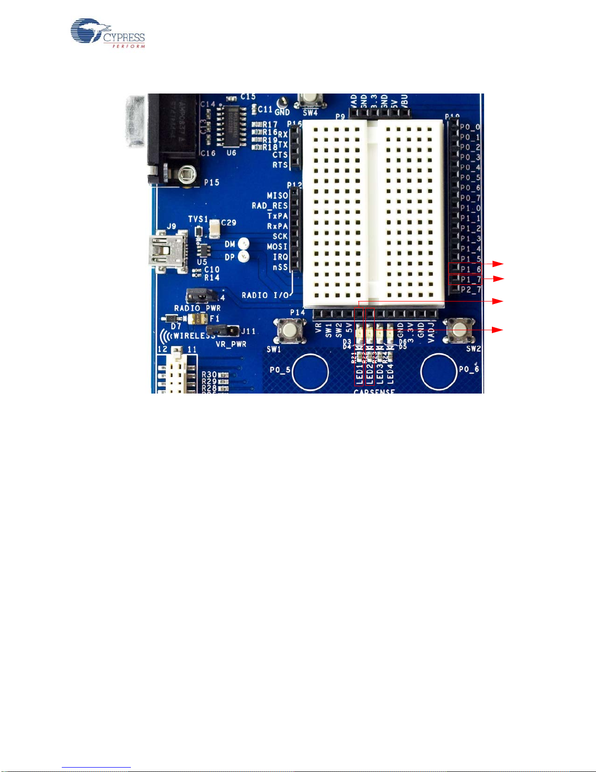
Figure 2-5. Connect P1[6] to LED1 and P1[7] to LED2
P1[6]
P1[7]
LED1
LED2
Loading My First PSoC Project
3. For more details regarding this project, see the detailed project instructions in My First PSoC 1
(CY8C28) Project on page 33.
CY8CKIT-001 PSoC Development Kit Guide, Doc. # 001-48651 Rev. *J 19
Page 20
Loading My First PSoC Project
2.2 My First PSoC 1 (CY8C29) Project
This is a simple PSoC 1 project using a PWM peripheral inside PSoC, and software to control the
blinking rates two different LED outputs. For this project, be sure you have the PSoC CY8C29 family
processor module inserted into the PSoC development board and the approp riate sof twar e inst alled.
This section walks you through the steps to open, build, and program a project.
2.2.1 Loading My First PSoC 1 Project
1. Open PSoC Designer.
2. In the Start Page, navigate to File
3. Navigate to the pr oje ct dir ec to ry: C:\Cypress\CY8CKIT-001\CY8C29 Projects.
4. Open the folder Example_My_First_PSoC_Project.
5. Double-click Example_My_First_PSoC_Project.app.
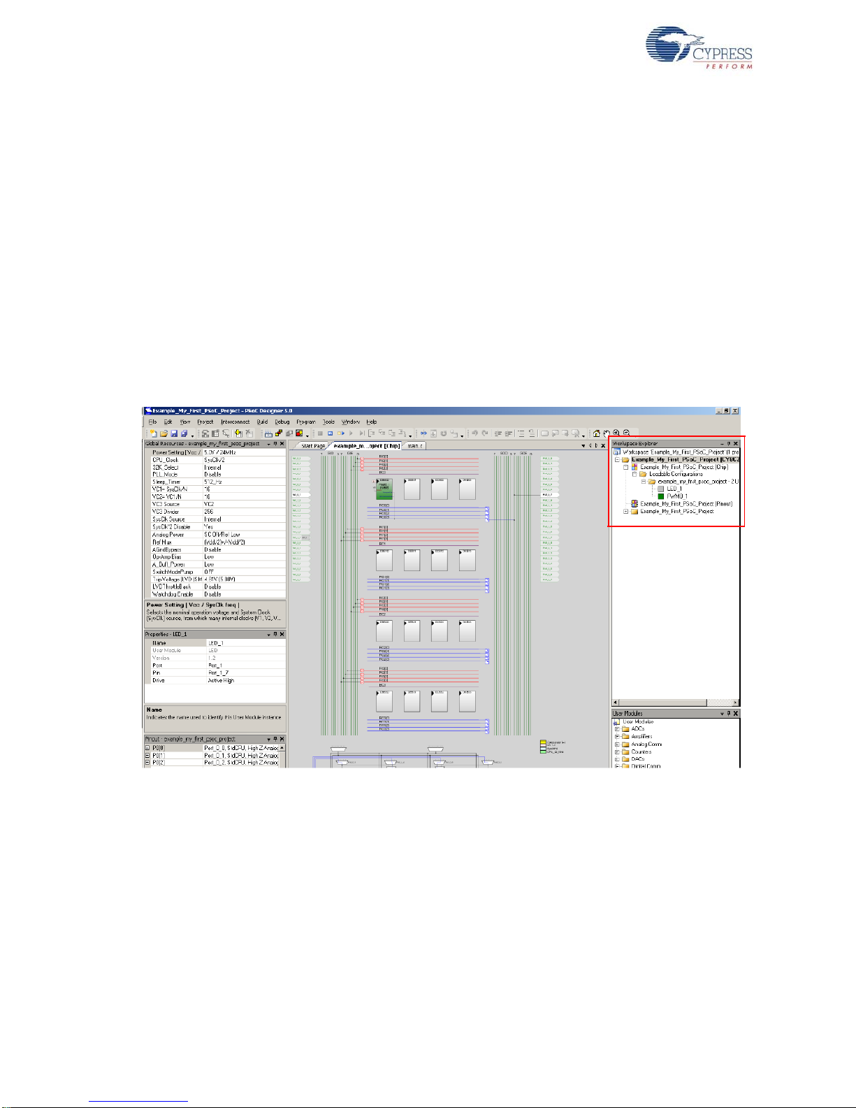
6. The project opens in the Chip Editor view. All project files are in the Workspace Explorer.
Figure 2-6. Chip Editor View
Open Project/Workspace.
20 CY8CKIT-001 PSoC Development Kit Guide, Doc. # 001-48651 Rev. *J
Page 21
2.2.2 Building My First PSoC 1 Project
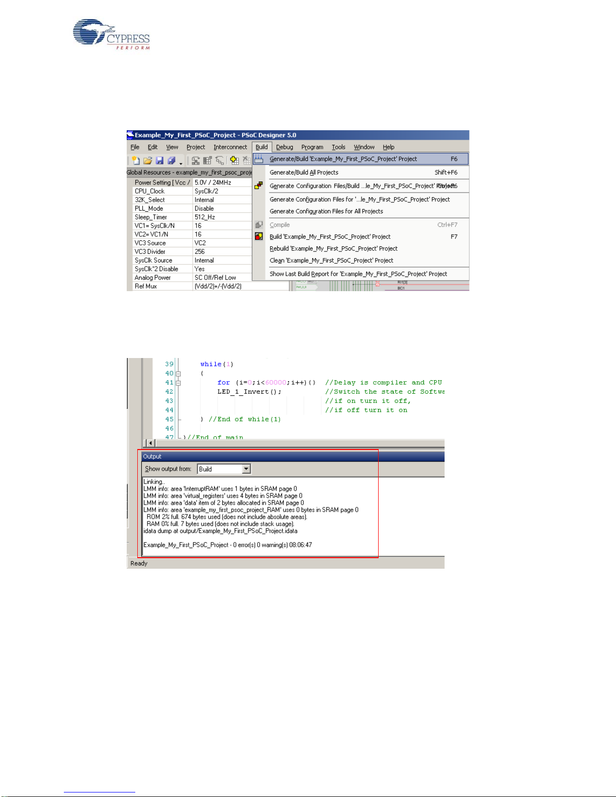
1. Select Build Generate/Build 'Example_My_First_PSoC_Project' Project.
Figure 2-7. Build Project
2. PSoC Designer builds the project and displays comments in the Output window. When you see
the message that the project is built with 0 errors and 0 warnings, you are ready to program the
device.
Loading My First PSoC Project
Figure 2-8. Output Window
CY8CKIT-001 PSoC Development Kit Guide, Doc. # 001-48651 Rev. *J 21
Page 22
Loading My First PSoC Project
2.2.3 Programming My First PSoC 1 Project
Figure 2-9. Connect MiniProg3 to J5 on CY8C29 Family Processor Module
1. Open PSoC Programmer from within PSoC Designer by selecting Program PSoC
Programmer.
2. In PSoC Programmer, make sure that MiniProg3 is selected in the Port Selection box.
3. In PSoC Programmer, set Programming Mode to Reset.
4. In PSoC Programmer, set Verification to On so that the software verifies that the downloaded
program's checksum matches the actual checksum of the flash memory after programming. This
is a precautionary check to verify that there is no data corruption during programming.
5. In PSoC Programmer, set AutoDetection to On to enable the software to automatically detect
and configure for the target device family and device. If PSoC Programmer is properly
configured, AutoDetection reports a device family of 29x66 and device of CY8C29466.
Note Make sure ISSP protocol is selected.
6. With these settings configured, click Program to program your PSoC 1 device.
7. Wait until programming is complete before continuing.
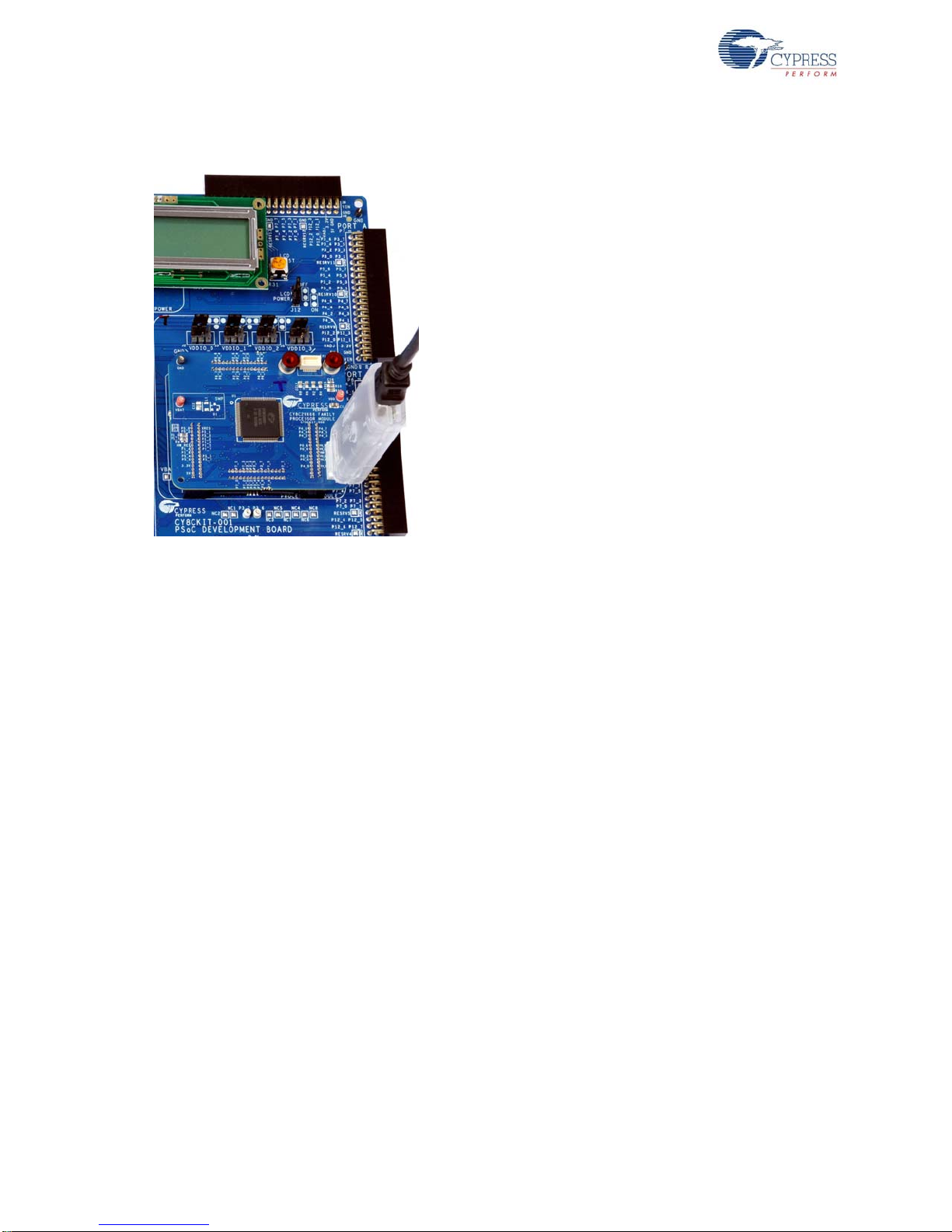
Note For debugging purposes, the CY8C29 family processor module is designed to accommodate
the use of the CY3215-DK In-Circuit Emulator (ICE-Cube). When using the ICE-Cube debugger,
make certain that PSoC Designer is configured so that the ICE-Cube does not provide power to the
processor module. Within the PSoC Designer application, select Project Settings and select
Debugger from the tree. Make sure that External only is selected under the Pod Power Source
section and select Execute Program from the Debug menu to start debugging.
Connect the processor module to the CY3215-DK ICE-Cube, as shown in Figure 2-10.
22 CY8CKIT-001 PSoC Development Kit Guide, Doc. # 001-48651 Rev. *J
Page 23
Loading My First PSoC Project
Figure 2-10. ICE-Cube Connected to CY8C29 (PSoC 1) Processor Module - Debugging the
Example_My_First_PSoC_Project Code Example
2.2.4 Running My First PSoC 1 Project
1. Connect P0[7] to LED1 and P1[7] to LED2. Verify that LED1 and LED2 are blin king base d on th e
project's use of the PWM and software. Now that the PSoC 1 device is programmed, reset the
PSoC development board by pressing and releasing the reset switch (SW4).
2. LED1 blinks approximately once every second and LED2 blinks about three times a second.
CY8CKIT-001 PSoC Development Kit Guide, Doc. # 001-48651 Rev. *J 23
Page 24
Loading My First PSoC Project
P0[7]
P1[7]
LED1
LED2
Figure 2-11. Connect P0[7] to LED1 and P1[7] to LED2
3. For more details regarding this project, see the detailed project instructions in My First PSoC 1
(CY8C29) Project on page 70.
24 CY8CKIT-001 PSoC Development Kit Guide, Doc. # 001-48651 Rev. *J
Page 25
2.3 My First PSoC 3 (CY8C38) Project
This is a PSoC 3 project using a PWM peripheral programmed from inside the PSoC 3 device to
control the blinking rates of two different LED outputs. For this project, insert the PSoC CY8C38 family processor module in the PSoC development board and install the appropriate software. This section shows you the steps to open, build, and program a project.
2.3.1 Loading My First PSoC 3 Project
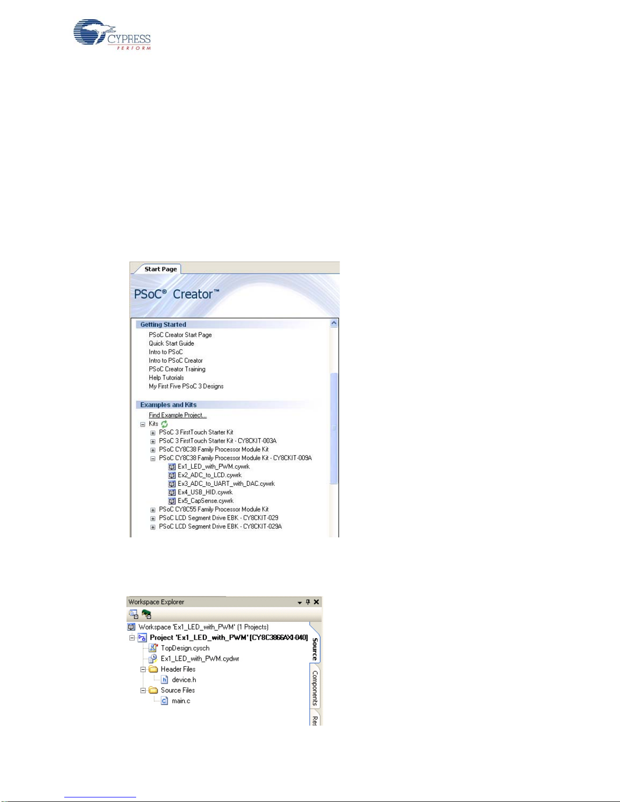
1. Open PSoC Crea tor.
2. In the Start Page, under Start Page Topics expand Kits.
3. Under Kits, expand PSoC CY8C38 Family Processor Module Kit.
4. Click Ex1_LED_with_PWM.cywrk to open the project.
Figure 2-12. Kits List
Loading My First PSoC Project
5. Select the directory to store the project.
6. After the project opens, you can se e the pr oje ct file s in Workspace Explorer (see Figure 2-13).
Figure 2-13. Workspace Explorer
CY8CKIT-001 PSoC Development Kit Guide, Doc. # 001-48651 Rev. *J 25
Page 26
Loading My First PSoC Project
2.3.2 Building My First PSoC 3 Project
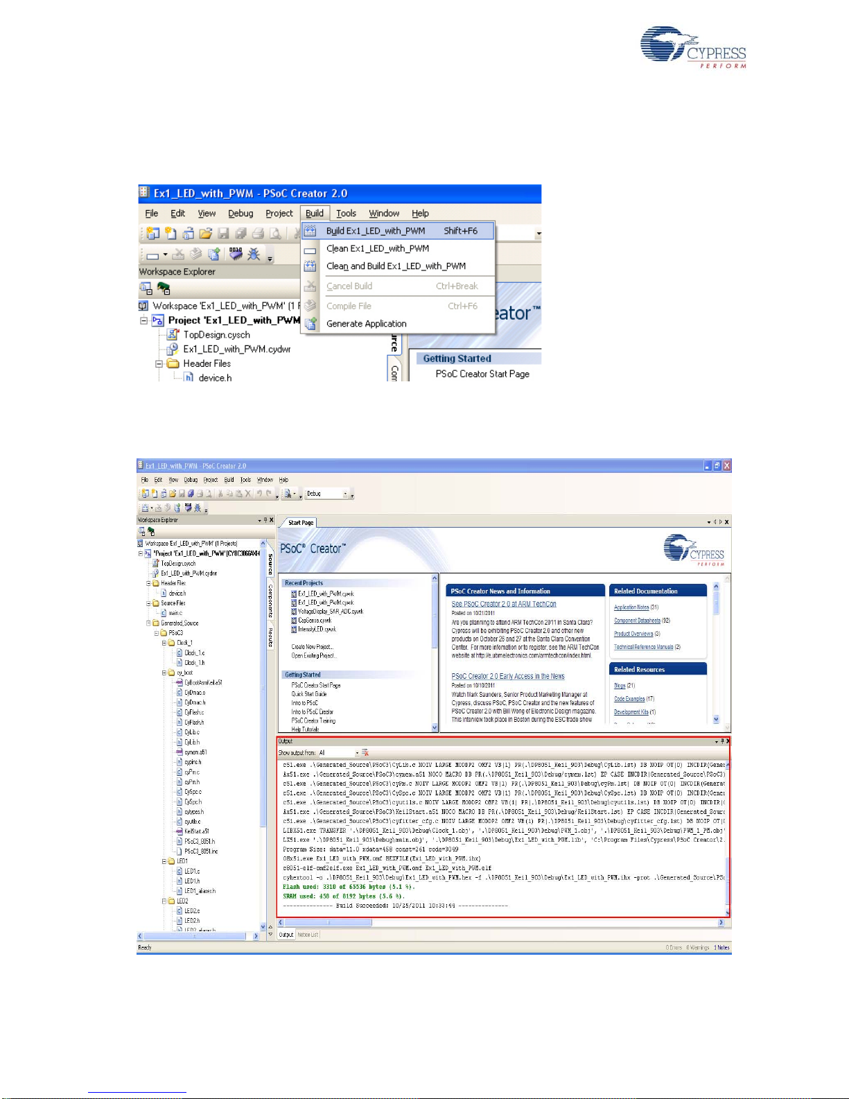
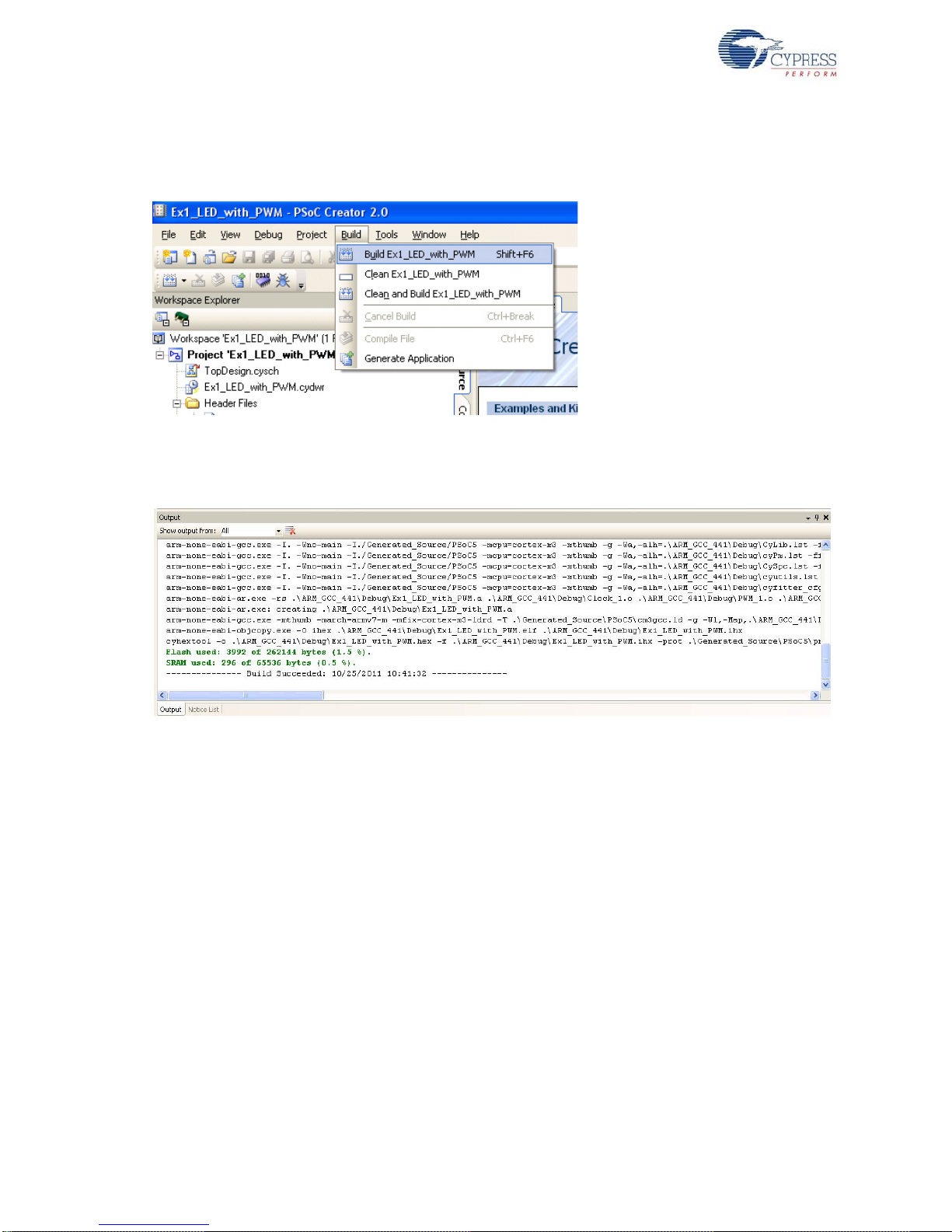
1. Select Build Build Ex1_LED_with_PWM.
Figure 2-14. Build Window
2. PSoC Creator builds the project and displays the comments in the Output window. When you
see the message "Build Succeeded", you are ready to program the device.
Figure 2-15. Output Window
26 CY8CKIT-001 PSoC Development Kit Guide, Doc. # 001-48651 Rev. *J
Page 27
2.3.3 Programming My First PSoC 3 Project
Figure 2-16. Connect MiniProg3 to J5 on CY8C38 Family Processor Module
Loading My First PSoC Project
1. If this is your first time running PSoC Creator, follow these steps to configure the MiniProg3
device for these PSoC development kit projects. If these configurations are set, skip to the next
step and begin programming.
Note VTARG of the MiniProg3 is wired exclusively to VDDIO1 of the chip on the PSoC CY8C38
family processor module. Because of this, you cannot perform power cycle mode programming.
❐ From the Tools menu in PSoC Creator, click Options. The Options window opens.
❐ In the Options window, select Program/Debug Port Configuration MiniProg3 from the
list.
•Set Power to 3.3 V
•Set Active Protocol to SWD
•Set Connector to 10 Pin
•Set Acquire Mode to Reset
•Set Clock Speed to 3.2 MHz
• Click OK.
❐ From the Debug menu, select Select Debug Target. The Select Debug Target dialog box
opens.
❐ Expand the tree under MiniProg3 and click Port Acquire.
❐ Select the appropriate device and click Connect.
❐ Click Close.
2. In PSoC Creator, from the Debug menu, click Program.
3. The PSoC Creator status bar indicates that the device is programming.
4. Wait until programming is complete before continuing.
CY8CKIT-001 PSoC Development Kit Guide, Doc. # 001-48651 Rev. *J 27
Page 28
Loading My First PSoC Project
P1[7]
P1[6]
LED1
LED2
2.3.4 Running My First PSoC 3 Project
1. Unplug the development board, switch SW3 to 3.3 V and then reapply power to the board.
2. Connect P1[6] to LED1 and P1[7] to LED2. Verify that LED1 and LED2 are blinkin g base d on the
project's use of the PWMs.
3. LED1 blinks approximately once every second and LED2 blinks about three times a second.
Figure 2-17. Connect P1[6] to LED1 and P1[7] to LED2
4. For more details regarding this project, review the detailed project instructions in My First PSoC 3
/ PSoC 5 Project on page 102.
2.4 My First PSoC 5 (CY8C55) Project
This project uses a PWM peripheral programmed from in sid e PSo C 5 to co nt rol the blinking rates of
two different LED outputs. For this project, insert the PSoC CY8C55 family processor module in the
PSoC development board and install the a ppropriate sof tware. This section shows the steps to ope n,
build, and program a project.
2.4.1 Loading my First PSoC 5 Project
1. Open PSoC Creato r.
2. In the Start Page, under Start Page Topics expand Kits.
3. Under Kits, expand PSoC CY8C55 Family Processor Module Kit.
4. Click Ex1_LED_with_PWM.cywrk to open the project.
28 CY8CKIT-001 PSoC Development Kit Guide, Doc. # 001-48651 Rev. *J
Page 29
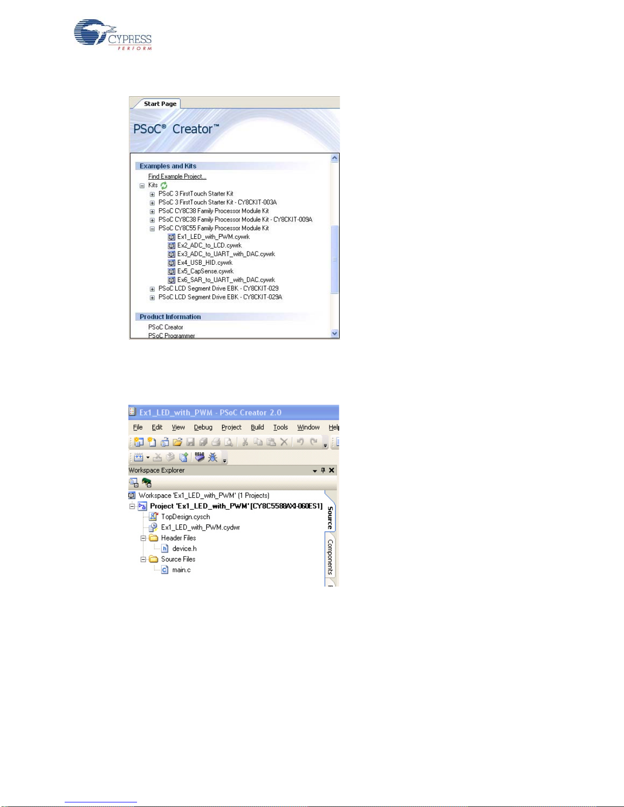
Figure 2-18. Kits List
Loading My First PSoC Project
5. Select the directory to store the project.
6. After the project ope ns, you can se e th e project files in Workspace Explorer.
Figure 2-19. Workspace Explorer
CY8CKIT-001 PSoC Development Kit Guide, Doc. # 001-48651 Rev. *J 29
Page 30
Loading My First PSoC Project
2.4.2 Building My First PSoC 5 Project
1. Select Build Build Ex1_LED_with_PWM.
Figure 2-20. Build Window
2. PSoC Creator builds the project and displays the comments in the Output window. When you see
the message "Build Succeeded", you are read y to pr og r am the dev ice .
Figure 2-21. Output Window
30 CY8CKIT-001 PSoC Development Kit Guide, Doc. # 001-48651 Rev. *J
Page 31

2.4.3 Programming My First PSoC 5 Project
Figure 2-22. Connect MiniProg3 to J5 on CY8C55 Family Processor Module
Loading My First PSoC Project
1. If this is your first time running PSoC Creator, follow these steps to configure the MiniProg3
device for these PSoC development kit projects. If these configurations are set, skip to the next
step and begin programming.
Note VTARG of the MiniProg3 is wired exclusively to VDDIO1 of the chip on the PSoC CY8C55
family processor module. Because of this, you cannot perform power cycle mode programming.
❐ From the Tools menu in PSoC Creator, click Options.
❐ In the Options window, select Program/Debug Port Configuration MiniProg3 from the
list.
•Set Power to 3.3 V
•Set Active Protocol to SWD
•Set Connector to 10 Pin
•Set Acquire Mode to Reset
•Set Clock Speed to 3.2 MHz
• Click OK
❐ From the Debug menu, select Select Debug Target.
❐ Expand the tree under MiniProg3 and click Port Acquire.
❐ Select the appropriate device and click Connect.
❐ Click Close.
2. In PSoC Creator, from the Debug menu, click Program.
3. The PSoC Creator status bar indicates that the device is programming.
4. Wait until programming is complete before continuing.
CY8CKIT-001 PSoC Development Kit Guide, Doc. # 001-48651 Rev. *J 31
Page 32

Loading My First PSoC Project
P1[7]
P1[6]
LED1
LED2
2.4.4 Running My First PSoC 5 Project
1. Unplug the development board, switch SW3 to 3.3 V and then reapply power to the board.
2. Connect P1[6] to LED1 and P1[7] to LED2. Verify that LED1 and LED2 are blinkin g base d on the
project's use of the PWMs.
3. LED1 blinks approximately once every second and LED 2 blinks about three times a second.
Figure 2-23. Connect P1[6] to LED1 and P1[7] to LED2
32 CY8CKIT-001 PSoC Development Kit Guide, Doc. # 001-48651 Rev. *J
Page 33

3. Sample Projects
This chapter shows you how to create the sample projects included with this kit.
Read these precautions before you create code examples:
■ All CY8C28 and CY8C29 family processor module code examples are configured for 5 V.
■ All CY8C38 and CY8C55 family processor module code examples are configured for 3.3 V.
■ Close any open project in PSoC Creator before loading or creating a code example.
■ When working with code examples, use the 12-V power supply adapter.
■ Remove power before changing board jumpers for each code example. Rea pply p ower af ter you
place jumpers on the breadboard.
■ When you complete each project make certain to save the project.
3.1 CY8C28 Family Processor Module Code Examples
3.1.1 My First PSoC 1 (CY8C28) Project
3.1.1.1 Creating My First PSoC 1 (CY8C28) Project
1. Open PSoC Designer.
2. To create a new project, click File
3. In the New Project window, select Chip-Level Project . Name the project Ex1_LED_with_PWM.
4. In the Location field, click Browse and navigate to the appropriate directory.
Figure 3-1. New Project Window
5. Click OK. The Select Project Type window opens.
New Project. The New Project window opens.
CY8CKIT-001 PSoC Development Kit Guide, Doc. # 001-48651 Rev. *J 33
Page 34

Sample Projects
Figure 3-2. Select Project Type Window
6. Under Select Target Device, click View Catal og.
7. The Device Catalog window opens. Click on the PSoC tab and scroll down to the CY8C28XXX
8. In this section, click the CY8C28645-24LTXI device; click Select.
section.
Figure 3-3. Device Catalog Window
9. Under Generate 'Main' File Using:, select C; then, click OK.
10.By default, the project opens in Chip view.
34 CY8CKIT-001 PSoC Development Kit Guide, Doc. # 001-48651 Rev. *J
Page 35

Figure 3-4. Default View.
Sample Projects
11.In the User Modules window, expand the PWMs folder.
Figure 3-5. User Modules Window
12.In this folder, right-click on PWM8 and select Place. The user module (UM) is placed in the first
available digital block.
CY8CKIT-001 PSoC Development Kit Guide, Doc. # 001-48651 Rev. *J 35
Page 36

Sample Projects
Figure 3-6. Place User Module PWM8
13.Click the placed PWM8_1 UM; the Properties window opens on the left side of the screen. Configure the PWM with the settings shown in the following figure. If the Properties window does not
appear, click View
Properties Window.
Figure 3-7. Properties Window
14.Next, route the PWM CompareOut signal to P1[7]. The first step is to configure the lookup table
(LUT) on Row_0_Output3.
36 CY8CKIT-001 PSoC Development Kit Guide, Doc. # 001-48651 Rev. *J
Page 37

Figure 3-8. Route PWM8 CompareOut Signal to P1[7]
15.Double-click the LUT, the Digital Interconnect window opens.
16.In this window, enable Row_0_Output_3_Drive_3 to connect to GlobalOutOdd_7.
Sample Projects
Figure 3-9. Digital Interconnect Window
17.Click Close.
18.Click on GlobalOutOdd_7. In the window that appears, configure Pin for Port_1_7.
CY8CKIT-001 PSoC Development Kit Guide, Doc. # 001-48651 Rev. *J 37
Page 38

Sample Projects
Figure 3-10. Configure Pin for Port_1_7
19.Click OK to continue.
20.In the User Modules window, expand the Misc Digital folder. In this folder, right-click LED and
select Place; this adds the UM to the project. This UM does not use digital or analog blocks. It
appears in Workspace Explorer
Ex1_LED_with_PWM[Chip]
Ex1_LED_with_PWM[CY8C28]
Loadable Configurations Ex1_LED_with_PWM - 2 User
Modules.
Figure 3-11. Workspace Explorer
21.Click the LED_1 UM and navigate to the Properties window. Configure the LED for P1[6].
Figure 3-12. Properties Window
22.Configure the Global Resources window to match the following figure.
38 CY8CKIT-001 PSoC Development Kit Guide, Doc. # 001-48651 Rev. *J
Page 39

Sample Projects
Figure 3-13. Global Resources Window
23.Open the existing main.c file in Workspace Explorer . Replace the existing main.c content with the
content of the embedded CY8C28_main_Ex1.c file, which is available within the attachments feature of this PDF document.
Figure 3-14. Workspace Explorer
24.Sa ve th e pr oje c t .
25.To bu ild the project, click Build
Generate/Build 'Ex1_LED_with_PWM' Project.
26.Disconnect power to the board.
27.Configure the DVK board SW3 to 5 V.
28.Configure the DVK breadboard using the included jumper wires:
❐ P1[6] to LED1
❐ P1[7] to LED2
29.Reapply power to the board.
30.Use PSoC De sig ner as de sc rib ed in Programming My First PSoC 1 Project on page 17 to
program the device.
31.Reset the DVK and observe the blinking LEDs.
32.Save and close the project.
CY8CKIT-001 PSoC Development Kit Guide, Doc. # 001-48651 Rev. *J 39
Page 40

Sample Projects
3.1.1.2 main.c
1. Open the existing main.c file within Workspace Explorer.
2. Replace the existing main.c content with the content of the embedded CY8C28_main_Ex1.c file,
which is available within the attachments feature of this PDF document.
Note To access the embedded attachments feature in the PDF, click on the paper clip icon located in
the lower left corner of the Adobe Reader application.
#include <m8c.h> /* Part specific constants and macros */
#include "PSoCAPI.h" /* PSoC API definitions for all User Modules */
/*******************************************************************************
* Function Name: main
********************************************************************************
*
* Summary:
* The main function initializes the PWM and starts the PWM clock which will
* blink LED1. Then the main loop is entered which delays enough for LED2 to
* blink at a quicker rate than LED1.
*
* Parameters:
* void
*
* Return:
* void
*
*******************************************************************************/
void main(void)
{
WORD i; /* Variable used for delay */
PWM8_1_Start(); /* Turn on the PWM to blink LED on P1.6 */
LED_1_Start(); /* Enable Software controlled LED */
/* The following loop controls the software LED connected to P1.7 */
while(1)
{
/* Delay time depends on compiler optimization levels and CPU clock */
for (i = 0; i < 60000; i++);// Gives approximately 450 msec delay with ImageCraft
// and 170 msec with HiTech
#ifdef HI_TECH_C
for (i = 0; i < 60000; i++);// Give some more delay if HiTech compiler is used.
for (i = 0; i < 40000; i++);
#else
#endif
/* Switch the state of Software LED (on or off) */
LED_1_Invert();
} /* End of while(1) */
} /* End of main */
/* [] END OF FILE */
40 CY8CKIT-001 PSoC Development Kit Guide, Doc. # 001-48651 Rev. *J
Page 41

3.1.2 ADC to LCD Project
This project demonstrates a 9 -bit delta-sigma analog-to-digital converter (ADC) by measuring the
voltage of the potentiometer center tap wiper and displaying the resu lt on th e LCD. Connect the vo ltage potentiometer (VR) to the ADC input P0[1]. The program reads the 9-bit ADC result and prints it
to the LCD.
3.1.2.1 Creating ADC to LCD Project
1. Follow steps 1 to 10 in section 3.1.1.1 on page 33; change the project name to
Ex2_ADC_to_LCD.
2. In the User Modules window, expand the ADCs folder and right-click DelSigPlus; select Place.
A window opens with multiple options for the DelSigPlus UM. Here, the DS1128 configuration is
used. Scroll down in the window to verify that this is the case.
Figure 3-15. Multiple User Module Window
Sample Projects
3. Click OK.
4. Verify that the DelSigPlus_1 UM is placed in ASC10.
5. In the User Modules window, expand the Amplifiers window. Right-click PGA and select Place.
Ensure that the PGA is placed in ACC00.
CY8CKIT-001 PSoC Development Kit Guide, Doc. # 001-48651 Rev. *J 41
Page 42

Sample Projects
Figure 3-16. Place PGA in ACC00
6. In the User Modules window, expand Misc Digital; right-click LCD and click Place.
7. Click PGA_1 and configure the properties to match this figure.
Figure 3-17. PGA_1 Properties
8. Click DelSigPlus_1 and configure the properties to match this figure.
Figure 3-18. DelSigPlus_1 Properties
42 CY8CKIT-001 PSoC Development Kit Guide, Doc. # 001-48651 Rev. *J
Page 43

9. Click LCD_1 and configure the properties to match this figure.
Figure 3-19. LCD_1 Properties
10.Configure the Global Resources to match the following figure.
Figure 3-20. Global Resources
Sample Projects
11.Ensure that AnalogColumn_InputMUX_0 is connected to Port_0_1. If it is not configured for
this port, double-click the mux and choose Port_0_1.
CY8CKIT-001 PSoC Development Kit Guide, Doc. # 001-48651 Rev. *J 43
Page 44

Sample Projects
Figure 3-21. AnalogColumn_InputMUX_0 Connected to Port_0_1
12.Ensure that AnalogColumn_Clock_0 is connected to VC1. If it is not, double-click the mux and
choose VC1.
Figure 3-22. AnalogColumn_Clock_0 Connected to VC1
44 CY8CKIT-001 PSoC Development Kit Guide, Doc. # 001-48651 Rev. *J
Page 45

Sample Projects
P0[1]
VR
R20
RESET
13.Open the existing main.c file within Workspace Explorer. Replace the existing main.c content with
the content of the embedded CY8C28_main_Ex2.c file, which is available within the attachment s
feature of this PDF document.
14.Sa ve th e pr oje c t .
15.To bu ild the project, click Build
Generate/Build 'Ex2_ADC_to_LCD' Project.
16.Disconnect power to the board.
17.Configure the DVK SW3 to 5 V.
18.Configure the DVK breadboard using the included jumper wires:
❐ P0[1] to VR
Figure 3-23. Connect P0[1] to VR
19.Reapply power to the board.
20.Use PSoC De sig ner as de sc rib ed in Programming My First PSoC 1 Project on page 17 to
program the device.
21.After programming the device, press the reset button and vary the pote ntiometer (R20) to see the
results on the LCD.
CY8CKIT-001 PSoC Development Kit Guide, Doc. # 001-48651 Rev. *J 45
Page 46

Sample Projects
Note The ADC output values may not reach full range due to potentiome ter and ADC limitations.
ADC values may fluctuate several counts due to system no ise, and if the potentiometer volt age is
at the edge of an ADC count.
22.Save and close the project.
3.1.2.2 main.c
1. Open the existing main.c file within Workspace Explorer.
2. Replace the existing main.c content with the content of the embedded CY8C28_main_Ex2.c file,
which is available within the attachments feature of this PDF document.
Note To access the embedded attachments feature in the PDF, click on the paper clip icon located in
the lower left corner of the Adobe Reader application.
#include <m8c.h> /* part specific constants and macros */
#include "PSoCAPI.h" /* PSoC API definitions for all User Modules */
/* LCD specific */
#define ROW_0 0 /* LCD row 0 */
#define ROW_1 1 /* LCD row 1 */
#define COLUMN_0 0 /* LCD column 0 */
#define COLUMN_9 9 /* LCD column 9 */
/*******************************************************************************
* Function Name: main
********************************************************************************
*
* Summary:
* The main function initializes both the ADC and LCD, starts and waits for an
* ADC conversion, then it displays the raw counts to the LCD.
*
* Parameters:
* void
*
* Return:
* void
*
*******************************************************************************/
void main(void)
{
WORD adcResult; /* Holds the integer ADC result */
/* Initialize the PGA used to buffer input from the potentiometer (VR) on
P0.1 to the ADC */
PGA_1_Start(PGA_1_HIGHPOWER);
DelSigPlus_1_Start(DelSigPlus_1_HIGHPOWER); /* Initialize the ADC */
LCD_1_Start(); /* Initialize the LCD */
LCD_1_Position(ROW_0, COLUMN_0); /* Set the LCD to (Row=0,Column=0) */
LCD_1_PrCString("V Count: ");
DelSigPlus_1_StartAD(); /* Start gathering conversions from the ADC */
M8C_EnableGInt; /* Enable Global interrupts */
/* This loop waits for a valid ADC result, and displays it on the LCD */
46 CY8CKIT-001 PSoC Development Kit Guide, Doc. # 001-48651 Rev. *J
Page 47

Sample Projects
while (1)
{
/* Is there ADC data? */
if(DelSigPlus_1_fIsDataAvailable())
{
/* Store result from ADC */
adcResult = DelSigPlus_1_wGetDataClearFlag();
LCD_1_Position(ROW_0, COLUMN_9); /* Set LCD to (Row=0,Column=9) */
LCD_1_PrHexInt(adcResult); /* Print ADC result on LCD */
}
} /* End of while(1) */
} /* End of main */
/* [] END OF FILE */
CY8CKIT-001 PSoC Development Kit Guide, Doc. # 001-48651 Rev. *J 47
Page 48

Sample Projects
3.1.3 ADC to UART with DAC
This project demonstrates sine wave generation by using a 6-bit digital-to-analog converter (DAC).
The sine wave period is based on the current value of the ADC. The firmware reads the voltage
output by the DVK board potentiometer and displays the raw counts on the DVK board character
LCD display similar to those shown in the previous project. A 6-bit DAC outputs a table generated
sine wave at a frequency proportional to the ADC count. The frequency outputs to an oscilloscope. A
38400 Baud UART outputs the current ADC count as ASCII formatted into a hexadecimal number.
3.1.3.1 Creating ADC to UART with DAC Project
1. Follow steps 1 to 10 in section 3.1.1.1 on page 33; change the project name to
Ex3_ADC_to_UART_with_DAC.
2. In the User Modules window expand the ADCs folder and right-click DelSigPlus; select Place.
A window opens with multiple options for the DelSigPlus UM. Here, the DS1128 configuration is
used. Scroll down in the window to verify that this is the case.
3. Click OK.
4. Verify that the UM is placed in ASC10.
5. In the User Modules window, expand the Amplifiers window. Right-click PGA and select Place.
Ensure that the PGA is placed in ACC00.
Figure 3-24. Place PGA in ACC00
6. In the User Modules window, expand Misc Digital, right-click LCD, and select Place.
7. In the User Modules window, expand Counters, right-click Counter16, and select Place.
8. In the User Modules window, expand Digital Comm, right-click TX8, and select Place.
9. In the User Modules window, expand DACs, right-click DAC6, and select Place. User module is
placed in ASD20 analog block by default. Drag and drop it to ASC21 block.
10.Move the UMs so that they match the configuration shown in Figure 3-25.
48 CY8CKIT-001 PSoC Development Kit Guide, Doc. # 001-48651 Rev. *J
Page 49

Figure 3-25. Configure User Modules
Counter16_1
Counter16_1
TX8_1
PGA_1
DelSigPlus_1
DAC6_1
Sample Projects
11.Click on DelSigPlus_1 and configure it to match this figure.
Figure 3-26. DelSigPlus_1 Properties
CY8CKIT-001 PSoC Development Kit Guide, Doc. # 001-48651 Rev. *J 49
Page 50

Sample Projects
12.Click PGA_1 and configure it to match this figure.
Figure 3-27. PGA_1 Properties
13.Click DAC6_1 and configure it to match this figure.
Figure 3-28. DAC6_1 Properties
14.Click LCD_1 and configure it to match this figure.
Figure 3-29. LCD_1 Properties
15.Click on Counter16_1 and configure it to match this figure.
Figure 3-30. Counter16_1 Properties
50 CY8CKIT-001 PSoC Development Kit Guide, Doc. # 001-48651 Rev. *J
Page 51

Sample Projects
16.Click TX8_1 and configure it to match this figure.
Figure 3-31. TX8_1 Properties
17.Click RO0[2] LUT, enable Row_0_Output_2_Drive_2 to connect GlobalOutOdd_2.
Figure 3-32. Digital Interconnect Window
CY8CKIT-001 PSoC Development Kit Guide, Doc. # 001-48651 Rev. *J 51
Page 52

Sample Projects
18.Click GlobalOutOdd_2. In the window that appears, configure Pin for Port_1_2.
Figure 3-33. Configure Pin for Port_1_2
19.Click OK to continue.
20.Click AnalogOutBuf_1 and configure it for Port_0_5.
Figure 3-34. Configure AnalogOutBuf_1
21.Verify that AnalogColumn_InputMUX_0 is connected to Port_0_1. If it is not configured for this
port, double-click the mux and choose Port_0_1.
52 CY8CKIT-001 PSoC Development Kit Guide, Doc. # 001-48651 Rev. *J
Page 53

Figure 3-35. AnalogColumn_InputMUX_0 Connection
Sample Projects
CY8CKIT-001 PSoC Development Kit Guide, Doc. # 001-48651 Rev. *J 53
Page 54

Sample Projects
22.Verify that AnalogColumn_Clock_0 and AnalogColumn_Clock_1 are connected to VC2. If it is
Figure 3-36. AnalogColumn_Clock_0 Connection
not, double-click the mux and chose VC2.
54 CY8CKIT-001 PSoC Development Kit Guide, Doc. # 001-48651 Rev. *J
Page 55

Sample Projects
23.Configure Global Resources to match the following figure.
Figure 3-37. Configure Global Resources
24.Open the existing main.c file within Workspace Explorer. Replace the existing main.c content with
the content of the embedded CY8C28_main_Ex3.c file, which is available within the attachment s
feature of this PDF document.
25.Sa ve th e pr oje c t .
26.To generate the project, click Build
Generate/Build 'Ex3_ADC_to_UART_with_DAC'
Project.
27.Ope n yo ur boot.tpl file in the project folde r Files
Open File. Select All Files for Files of the
type:.
28.Select boot.tpl in the list of files and click Open.
29.Find the line '@INTERRUPT_9' (for PSoC Block DBC01) and replace that line with:
ljmp_Counter16_C_ISR
30.Sa ve th e pr oje c t .
31.To bu ild the project, click Build
Build 'Ex3_ADC_to_UART_with_DAC' Project.
32.Disconnect power to the board.
33.Configure the DVK SW3 to 5 V.
34.Configure the DVK breadboard using the included jumper wires as follows:
❐ P0[1] to VR
❐ P1[2] to TX
❐ P0[5] to Scope
Note An LED (P0[5] to LED1) by nature does not accurately show the changes in frequency
the best way to see this is to use a Scope(P0[5] to Scope).
CY8CKIT-001 PSoC Development Kit Guide, Doc. # 001-48651 Rev. *J 55
Page 56

Sample Projects
P0[1]
VR
P1[2]
TX
Figure 3-38. Connect P0[1] to VR, P1[2] to TX, and P0[5] to LED1
35.Connect a serial cable to the PC and the DVK board.
36.On the DVK board, verify that RS232_PWR(J10) is jumpered to ON.
37.Reapply power to the board.
38.Use a terminal application such as TeraTerm or HyperTermina l with these setup parameters.
❐ Baud Rate: 38400
❐ Data: 8-bit
❐ Parity: none
❐ Stop: 1bit
❐ Flow Control: none
39.Use PSoC De sig ner as de sc rib ed in Programming My First PSoC 1 Project on page 17 to
program the device.
After programming the device, press Reset and vary the pot to see the result on the LCD as well
as in the terminal application. View the DAC output on a scope or with an LED.
Note The ADC output values may not reach full range due to potentiome ter and ADC limitations.
ADC values may fluctuate several counts due to system no ise, and if the potentiometer volt age is
at the edge of an ADC count.
40.Save and close the project.
56 CY8CKIT-001 PSoC Development Kit Guide, Doc. # 001-48651 Rev. *J
Page 57

3.1.3.2 main.c
1. Open the existing main.c file within Workspace Explorer.
2. Replace the existing main.c content with the content of the embedded CY8C28_main_Ex3.c file,
which is available within the attachments feature of this PDF document.
Note To access the embedded attachments feature in the PDF, click on the paper clip icon located in
the lower left corner of the Adobe Reader application.
#include <m8c.h> /* part specific constants and macros */
#include "PSoCAPI.h" /* PSoC API definitions for all User Modules */
/* Counter16 Interrupt Handler */
#pragma interrupt_handler Counter16_C_ISR
/* LCD specific */
#define ROW_0 0 /* LCD row 0 */
#define ROW_1 1 /* LCD row 1 */
#define COLUMN_0 0 /* LCD column 0 */
#define COLUMN_9 9 /* LCD column 9 */
const BYTE sinTable[]=
{
0, 0, 1, 2, 3, 4, 6, 7, 10, 12, 14, 17, 20, 23, 26, 29,
31, 33, 36, 39, 41, 44, 46, 49, 51, 53, 55, 56, 58, 59, 59, 60,
60, 60, 59, 59, 58, 56, 55, 53, 51, 49, 47, 44, 42, 39, 36, 33,
31, 28, 25, 22, 19, 16, 13, 11, 9, 7, 5, 3, 2, 1, 0, 0
};
Sample Projects
BYTE tablePos = 0;
/*******************************************************************************
* Function Name: main
********************************************************************************
*
* Summary:
* The main function initializes the ADC, PGA, LCD, Counter, DAC and UART.
* In the main loop, it continuously checks for an ADC conversion. If there is
* one then it displays the ADC raw count to the LCD, transmits the raw count
* serially, and updates the Counter16 period (based on the raw count) for the
* DAC output.
*
* Parameters:
* void
*
* Return:
* void
*
*******************************************************************************/
void main(void)
{
/* Variable for holding ADC result, and updating counter period */
WORD adcResult;
Counter16_1_Start(); /* Enable the counter used for DAC update rate */
Counter16_1_EnableInt(); /* Enable DAC update interrupt */
CY8CKIT-001 PSoC Development Kit Guide, Doc. # 001-48651 Rev. *J 57
Page 58

Sample Projects
/* Start the TX8 UM with no parity (baud rate = 38400) */
TX8_1_Start(TX8_1_PARITY_NONE);
/* Enable to PGA to buffer signal from VR to ADC */
PGA_1_Start(PGA_1_HIGHPOWER);
DAC6_1_Start(DAC6_1_HIGHPOWER); /* Start the DAC */
DelSigPlus_1_Start(DelSigPlus_1_HIGHPOWER); /* Start the ADC */
DelSigPlus_1_StartAD(); /* Start reading values on the ADC */
LCD_1_Start(); /* Start the character LCD */
LCD_1_Position(ROW_0, COLUMN_0); /* Set the LCD to (Row=0,Column=0) */
LCD_1_PrCString("V Count: ");
M8C_EnableGInt; /* Enable Global Interrupts */
while(1)
{
/* Step 1: Get BYTE data from the ADC
Step 2: Write BYTE data from ADC to the counter to
change the DAC update rate
Step 3: Move the LCD cursor back to the beginning and display new
ADC data
Step 4: Write ADC data out the TX port, and then send a return
*/
/* Is new data available from the ADC? */
if (DelSigPlus_1_fIsDataAvailable())
{
adcResult = DelSigPlus_1_wGetDataClearFlag(); /* Get new ADC data */
/* Change DAC update rate counter */
Counter16_1_WritePeriod((adcResult << 4) + 200);
LCD_1_Position(ROW_0, COLUMN_9); /* Move LCD (row=0,column=0) */
LCD_1_PrHexInt(adcResult); /* Print ADC result to LCD */
TX8_1_PutSHexInt(adcResult); /* Write LCD result to TX8 -> PC */
TX8_1_PutCRLF(); /* Write return character to TX8 */
}
} /* End of while(1) */
} /* End of Main */
/*******************************************************************************
* Function Name: Counter16_C_ISR
********************************************************************************
*
* Summary:
* This is the interrupt service routine for the Counter16 usermodule written
* in C. The boot.tpl has been modified to jump to this ISR every terminal
* count. The related #pragma above is necessary for the boot.asm file to jump
* to it. Every time a terminal count is reached the DAC will get the next
* value from the sinTable.
*
* Parameters:
* void
*
* Return:
* void
58 CY8CKIT-001 PSoC Development Kit Guide, Doc. # 001-48651 Rev. *J
Page 59

Sample Projects
*
*******************************************************************************/
#ifdef HI_TECH_C
void Counter16_C_ISR(void) @ 0x24
#else
void Counter16_C_ISR(void)
#endif
{
// Check to see if we have reached the //
if (tablePos >= sizeof(sinTable))
{
tablePos = 0;
}
DAC6_1_WriteBlind(sinTable[tablePos++]);
}
/* [] END OF FILE */
CY8CKIT-001 PSoC Development Kit Guide, Doc. # 001-48651 Rev. *J 59
Page 60

Sample Projects
3.1.4 CapSense
This project demonstrates CapSense . The firmware displays the CapSense button pre sses on the
LCD (row 1) and associated LEDs. It also displays the CapSense slider position on the LCD (row 2).
Note that this project uses IDAC. But if you are using an external Rb with CSD, then populate R15
(connected to P3[1]). Rb can range from 2 k to 10 k. See the CapSense user module datasheet for
more information on using Rb.
3.1.4.1 Creating CapSense Project
1. Follow steps 1 to 10 in section 3.1.1.1 on page 33; change the project name to Ex4_CapSense.
2. In the User Modules window, expand the Cap Sensors folder. Right-click CSD and select Place.
A window appears with the option to use the default configuration.
Figure 3-39. Select Multi User Module Window
3. Select Yes and click OK.
4. Right-click the CSD user module in the workspace explorer and select CSD Wizard.
Figure 3-40. Select CSD Wizard
60 CY8CKIT-001 PSoC Development Kit Guide, Doc. # 001-48651 Rev. *J
Page 61

5. The CapSense Wizard window opens.
Figure 3-41. CapSense Wizard
Sample Projects
6. In the CapSense Wizard window, under the Global Settings tab, set the # of buttons to ‘2’.
7. Select P0[7] as the Modulator Capacitor Pin.
Figure 3-42. CapSense Wizard Place Buttons
CY8CKIT-001 PSoC Development Kit Guide, Doc. # 001-48651 Rev. *J 61
Page 62

Sample Projects
8. Click and hold SW0 and drag it to P0[5].
9. Click and hold SW1 and drag it to P0[6].
Figure 3-43. CapSense Wizard Slider Sensors
10. Repeat for each slider sensor and corresponding pin.
❐ S0[0] to P0[0]
❐ S0[1] to P0[1]
❐ S0[2] to P0[2]
❐ S0[3] to P0[3]
❐ S0[4] to P0[4]
11.Select the Sensors Settings tab.
12.Set the Resolution to 80.
62 CY8CKIT-001 PSoC Development Kit Guide, Doc. # 001-48651 Rev. *J
Page 63

Figure 3-44. Sensors Settings Tab
Sample Projects
13.Click OK.
14.In the User Modules window, expand Misc Digital, right-click LCD, and select Place.
15.In the User Modules window, expand Misc Digital, right-click LED, and select Place.
16.In the User Modules window, expand Misc Digital, right-click LED, and select Place.
17.Click CSD_1 and configure it to match this figure.
Figure 3-45. CSD_1 Properties
18. Click LCD_1 and configure it to match this figure.
CY8CKIT-001 PSoC Development Kit Guide, Doc. # 001-48651 Rev. *J 63
Page 64

Sample Projects
Figure 3-46. LCD_1 Properties
19. Click LED_1 and configure it to match this figure.
Figure 3-47. LED_1 Properties
20.Click LED_2 and configure it to match this figure.
Figure 3-48. LED_2 Properties
21.Configure Global Resources to match the following figure.
Figure 3-49. Configure Global Resources
22.Open the existing main.c file within Workspace Explorer. Replace the existing main.c content with
the content of the embedded CY8C28_main_Ex4.c file, which is available within the attachment s
feature of this PDF document.
23.Sa ve th e pr oje c t .
24.To generate and build the project, click Build
Generate/Build 'Ex4_CapSense' Project.
25.Disconnect power to the board.
64 CY8CKIT-001 PSoC Development Kit Guide, Doc. # 001-48651 Rev. *J
Page 65

Sample Projects
26.Configure the DVK board SW3 to 5 V.
27.Configure the DVK breadboard using the included jumper wires:
❐ P1[6] to LED1
❐ P1[7] to LED2
28.Ensure that P0[1], P0[5], and P0[7] are disconnected.
29.Reapply power to the board.
30.Use PSoC De sig ner as de sc rib ed in Programming My First PSoC 1 Project on page 17 to
program the device.
31.Reset the DVK. An LED lights up when either CapSense button is pushed. If B1 (P0[5]) is
pushed, it also displays "Button1" in the top row of the LCD display. Similarly, if B2 (P0[6]) is
pushed, it displays "Button2" in the top row of the LCD display. The bottom row of the LCD displays the slider position with a horizontal bargraph.
32.Save and close the project.
CY8CKIT-001 PSoC Development Kit Guide, Doc. # 001-48651 Rev. *J 65
Page 66

Sample Projects
3.1.4.2 main.c
1. Open the existing main.c file within Workspace Explorer.
2. Replace the existing main.c content with the content of the embedded CY8C28_main_Ex4.c file,
which is available within the attachments feature of this PDF document.
Note To access the embedded attachments feature in the PDF, click on the paper clip icon located in
the lower left corner of the Adobe Reader application.
#include <m8c.h> /* part specific constants and macros */
#include "PSoCAPI.h" /* PSoC API definitions for all User Modules */
/* LCD specific */
#define ROW_0 0 /* LCD row 0 */
#define ROW_1 1 /* LCD row 1 */
#define COLUMN_0 0 /* LCD column 0 */
#define NUM_CHARACTERS 16 /* Number of characters on LCD */
/* For clearing a row of the LCD*/
#define CLEAR_ROW_STR " "
/* Button 1 only string for row 0 of the LCD */
#define BUTTON_1_STR "Button1 "
/* Button 2 only string for row 0 of the LCD */
#define BUTTON_2_STR " Button2"
/* Button 1 and 2 string for row 0 of the LCD */
#define BUTTON_1_2_STR "Button1 Button2"
/* Default string for button row of the LCD */
#define DEFAULT_ROW_0_STR "Touch Buttons "
/* Default string for slider row of the LCD */
#define DEFAULT_ROW_1_STR "Touch The Slider"
/* CapSense specific */
#define SLIDER_RESOLUTION 80
#define SCANSENSOR_BTN_B1 0
#define SCANSENSOR_BTN_B2 1
void UpdateButtonState(BYTE sensor_1, BYTE sensor_2);
void UpdateSliderPosition(BYTE value);
/*******************************************************************************
* Function Name: main
********************************************************************************
*
* Summary:
* The main function initializes CapSense and the LCD. Then it continuously
* scans all CapSense sensors (slider sensors and buttons), gets the state of
* the buttons and slider and updates the LCD with the current state.
*
* Parameters:
* void
*
* Return:
* void
*
*******************************************************************************/
void main(void)
{
66 CY8CKIT-001 PSoC Development Kit Guide, Doc. # 001-48651 Rev. *J
Page 67

Sample Projects
BYTE pos; /* Slider Position */
BYTE stateB_1; /* Button1 State */
BYTE stateB_2; /* Button2 State */
M8C_EnableGInt; /* Enable Global Interrupts */
/* LCD Initialization */
LCD_1_Start();
/* For Bargraph display on LCD */
LCD_1_InitBG(LCD_1_SOLID_BG);
/* LED1 Initialization */
LED_1_Start();
/* LED2 Initialization */
LED_2_Start();
/* CapSense Initialization */
CSD_1_Start();
/* Initialize the baselines by scanning all sensors and getting the initial
raw data values */
CSD_1_InitializeBaselines();
/* Load finger thresholds set in user module parameters */
CSD_1_SetDefaultFingerThresholds();
while(1)
{
/* Scan each CapSense sensor and update their raw data value */
CSD_1_ScanAllSensors();
/* Update baselines for each sensor */
CSD_1_UpdateAllBaselines();
/* Update state to active/inactive for each button sensor */
stateB_1 = CSD_1_bIsSensorActive(SCANSENSOR_BTN_B1);
stateB_2 = CSD_1_bIsSensorActive(SCANSENSOR_BTN_B2);
/* Get Linear Slider Position */
pos = CSD_1_wGetCentroidPos(1);
/* Update LCD and LED's with current Button and Linear Slider states */
UpdateButtonState(stateB_1, stateB_2);
UpdateSliderPosition(pos);
}
}
/*******************************************************************************
* Function Name: UpdateButtonState
********************************************************************************
*
* Summary:
* Updates the LCD screen with the current button state by displaying which
* button is being touched on row 0. LED's are also updated according to button
* state.
*
* Parameters:
* sensor_1: Button state for B1
* sensor_2: Button state for B2
*
* Return:
CY8CKIT-001 PSoC Development Kit Guide, Doc. # 001-48651 Rev. *J 67
Page 68

Sample Projects
* void
*
*******************************************************************************/
void UpdateButtonState(BYTE sensor_1, BYTE sensor_2)
{
LCD_1_Position(ROW_0,COLUMN_0);
/* Check the state of the buttons and update the LCD and LEDs */
if (sensor_1 && sensor_2)
{
/* Display both Button strings on LCD if both button sensors are active */
LCD_1_PrCString(BUTTON_1_2_STR);
/* Both LED's are on in this state */
LED_1_On();
LED_2_On();
}
else if (sensor_1 || sensor_2)
{
if (sensor_1)
{
/* Display Button 1 state on LCD and LED1 */
LCD_1_PrCString(BUTTON_1_STR);
LED_1_On();
/* Button 2 is not active */
LED_2_Off();
}
else // sensor_2
{
/* Display Button 2 state on LCD and LED2 */
LCD_1_PrCString(BUTTON_2_STR);
LED_2_On(); /* Turn on LED2 */
LED_1_Off(); /* Turn off the LED1 */
}
}
else
{
/* Display default string on LCD and set LED's to off */
LCD_1_PrCString(DEFAULT_ROW_0_STR);
/* Set both LED's off in this state */
LED_1_Off();
LED_2_Off();
}
}
/*******************************************************************************
* Function Name: UpdateSliderPosition
********************************************************************************
*
* Summary:
* Updates the LCD screen with the current slider position by displaying the
* horizontal bargraph.
*
* Parameters:
* value: Centroid position from CapSense slider.
*
* Return:
* void
*
68 CY8CKIT-001 PSoC Development Kit Guide, Doc. # 001-48651 Rev. *J
Page 69

Sample Projects
*******************************************************************************/
void UpdateSliderPosition(BYTE value)
{
/* The slider position is 0xFF if there is no finger present on the slider */
if (value > SLIDER_RESOLUTION)
{
/* Clear old slider position (2nd row of LCD) */
LCD_1_Position(ROW_1, COLUMN_0);
LCD_1_PrCString(DEFAULT_ROW_1_STR);
}
else
{
/* Update the bargraph with the current finger position */
LCD_1_DrawBG(ROW_1, COLUMN_0, NUM_CHARACTERS, value + 1);
}
}
/* [] END OF FILE */
CY8CKIT-001 PSoC Development Kit Guide, Doc. # 001-48651 Rev. *J 69
Page 70

Sample Projects
3.2 CY8C29 Family Processor Module Code Examples
3.2.1 My First PSoC 1 (CY8C29) Project
3.2.1.1 Creating My First PSoC 1 (CY8C29) Project
1. Open PSoC Designer
2. To create a new project, click File
3. In the New Project window, select the Chip-Level Project. Name the project
Example_My_First_PSoC_Project.
4. In the Location field, click Browse and navigate to the appropriate directory.
Figure 3-50. New Project Window
New Project. The New Project window opens.
5. Click OK. The Select Project Type window opens.
70 CY8CKIT-001 PSoC Development Kit Guide, Doc. # 001-48651 Rev. *J
Page 71

Figure 3-51. Select Project Type Window
Sample Projects
6. In this window, under Select Target Device, click View Catalog.
7. The Device Catalog window opens. Click on the PSoC tab, and scroll down to the CY8C29466,
CY8C29566,… section.
8. For this project, click any device in this section and then click Select.
Figure 3-52. Device Catalog Window
9. Under Generate 'Main' File Using:, select C, then click OK.
CY8CKIT-001 PSoC Development Kit Guide, Doc. # 001-48651 Rev. *J 71
Page 72

Sample Projects
10.By default, the project opens in Chip view.
Figure 3-53. Default View.
11.In the User Modules window, expand the PWMs folder.
Figure 3-54. User Modules Window
12.In this folder, right-click on PWM8 and select Place. The User Module (UM) is placed in the first
available digital block.
72 CY8CKIT-001 PSoC Development Kit Guide, Doc. # 001-48651 Rev. *J
Page 73

Figure 3-55. Place User Module PWM8
Sample Projects
13.Double-click the placed PWM8_1 UM; the Properties window opens on the left side of the
screen. Configure the PWM with the settings as in the following figure. If the Properties window
does not appear, click View
Properties Window.
Figure 3-56. Properties Window
CY8CKIT-001 PSoC Development Kit Guide, Doc. # 001-48651 Rev. *J 73
Page 74

Sample Projects
14.Next, route the PWM CompareOut signal to P0[7]. The first step is to configure the lookup table
Figure 3-57. Route the PWM CompareOut signal to P0[7]
(LUT) on Row_0_Output3.
15.Double-click the LUT, the Digital Interconnect window opens.
16.In this window, enable Row_0_Output_3_Drive_1 to connect to GlobalOutEven_7.
Figure 3-58. Digital Interconnect Window
17.Click Close.
18.Click on GlobalO utEven_7. In the window that appears, configure Pin for Port_0_7.
74 CY8CKIT-001 PSoC Development Kit Guide, Doc. # 001-48651 Rev. *J
Page 75

Figure 3-59. Configure Pin for Port_0_7
Sample Projects
19.Click OK to continue.
20.In the User Modules window expand the Misc Digital folder. In this folder, right-click the LED
and select Place; this adds the UM to the project. This UM does not use digital o r analo g bl ocks.
It appears in Workspace Explorer
Example_My_First_PSoC_Project[Chip]
Example_My_First_PSoC_Project[CY8C29]
Loadable Configurations
example_my_first_psoc_project - 2 Use r Modules.
Figure 3-60. Workspace Explorer
21.Double-click the LED_1 UM and navigate to the Properties window. Configure the LED for
Port_1_7.
Figure 3-61. Properties Window
CY8CKIT-001 PSoC Development Kit Guide, Doc. # 001-48651 Rev. *J 75
Page 76

Sample Projects
22.Configure the Global Resources window to match the following figure.
Figure 3-62. Global Resources Window
23.Open the existing main.c file within Workspace Explorer. Replace the existing main.c content with
the content of the embedded CY8C29_main_Ex1.c file, which is available within the attachment s
feature of this PDF document.
Figure 3-63. Workspace Explorer
24.Sa ve th e pr oje c t .
25.To build the project, click Build
Generate/Build 'Example_My_First_PSoC_Project' Project.
26.Disconnect power to the board.
27.Configure the DVK board SW3 to 5 V.
28.Configure the DVK breadboard using the included jumper wires:
❐ P0[7] to LED1
❐ P1[7] to LED2
29.Reapply power to the board.
30.Use PSoC De sig ner as de sc rib ed in Programming My First PSoC 1 Project on page 22 to program the device.
31.Reset the DVK, and observe the blinking LEDs.
32.Save and close the project.
76 CY8CKIT-001 PSoC Development Kit Guide, Doc. # 001-48651 Rev. *J
Page 77

3.2.1.2 main.c
1. Open the existing main.c file within Workspace Explorer.
2. Replace the existing main.c content with the content of the embedded CY8C29_main_Ex1.c file,
which is available within the attachments feature of this PDF document.
Note To access the embedded attachments feature in the PDF, click on the paper clip icon located in
the lower left corner of the Adobe Reader application.
/*******************************************************************************
* File Name: main.c
*
* Description:
* This file provides source code for My First PSoC Project example. The
* firmware blinks one LED at about 3.6 Hz with a PWM, and blinks another LED
* with a software timing loop.
*
********************************************************************************/
/******************************************************************************
* PWM Settings:
*
* Input Clock = VC3 //VC3 = 24 MHz/16/16/256 =366.2 Hz
* Enable = High
* CompareOut = ROW_0_Output_3
* TerminalCountOut = None
* Period = 100 Output period = (Period+1)*(1/Input Clock) = 101/
366.2 = .275 sec
* PulseWidth = 50
* CompareType = Less Than Or Equal
* InterruptType = Terminal Count
* ClockSync = Sync to SysClk
* InvertEnable = Normal
*
*********************************************************************************
/
Sample Projects
or 3.6 Hz
#include <m8c.h> // part specific constants and macros
#include "PSoCAPI.h" // PSoC API definitions for all User Modules
unsigned int i; // Variable used for delay
void main(void)
{
PWM8_1_Start();// Turn on the PWM to blink LED on P0.7
LED_1_Start();// Enable Software controlled LED
// The following loop controls the software LED connected to P1.7
while(1)
{
for (i=0;i<60000;i++){} //Length of delay depends on compiler and CPU clock
LED_1_Invert(); //Switch the state of Software LED, if on turn it off,
//if off turn it on
} //End of while(1)
}//End of main
CY8CKIT-001 PSoC Development Kit Guide, Doc. # 001-48651 Rev. *J 77
Page 78

Sample Projects
3.2.2 ADC to LCD Project
This project demonstrates a 9-bit Delta-Sigma ADC by measuring the voltage of the potentiometer
center tap wiper and displaying the result on the LCD. Connect th e volta ge potentiometer (VR) to th e
ADC input P0[1]. The program reads the 9-bit ADC result and prints it to the LCD.
3.2.2.1 Creating ADC to LCD Project
1. Follow steps 1 to 10 in section 3.2.1.1 on page 70; change the project name to
Example_ADC_to_LCD.
2. In the User Modules window, expand the ADCs folder; right-click DelSig and select Place. A
window opens with multiple options for the DelSig UM. Scroll down, if necessary, and select the
DS1128 configuration. Click OK.
Figure 3-64. Select Multi User Module Window
3. Click OK.
4. Verify that the DelSig_1 UM is placed in ASC10.
5. In the User Modules window, expand the Amplifiers window. Right-click PGA and select Place.
Ensure that the PGA is placed in ACB00.
78 CY8CKIT-001 PSoC Development Kit Guide, Doc. # 001-48651 Rev. *J
Page 79

Figure 3-65. Place PGA in ACB00
Sample Projects
6. In the User Modules window, expand Misc Digital; right-click LCD and select Place.
7. Double-click PGA_1 and configure the properties to match this figure.
Figure 3-66. PGA_1 Properties
8. Double-click DelSig_1 and configure the properties to match this fi gu re .
Figure 3-67. DelSig_1 Properties
9. Double-click LCD_1 and configure the properties to match this figure.
CY8CKIT-001 PSoC Development Kit Guide, Doc. # 001-48651 Rev. *J 79
Page 80

Sample Projects
Figure 3-68. LCD_1 Properties
10.Configure the Global Resources to match the following figure.
Figure 3-69. Global Resources Properties
11.Ensure that AnalogColumn_InputMUX_0 is connected to Port_0_1. If it is not configured for
this port, double-click the mux and choose Port_0_1.
80 CY8CKIT-001 PSoC Development Kit Guide, Doc. # 001-48651 Rev. *J
Page 81

Figure 3-70. AnalogColumn_InputMUX_0 is Connected to Port_0_1
Sample Projects
12.Ensure that AnalogColumn_Clock_0, is connected to VC1. If it is not, double-click the mux and
chose VC1.
Figure 3-71. AnalogColumn_Clock_0 is connected to VC1
13.Open the existing main.c file within Workspace Explorer. Replace the existing main.c content with
the content of the embedded CY8C29_main_Ex2.c file, which is available within the attachment s
feature of this PDF document.
14.Sa ve th e pr oje c t .
15.To bu ild the project, click Build
CY8CKIT-001 PSoC Development Kit Guide, Doc. # 001-48651 Rev. *J 81
Generate/Build 'Example_ADC_to_LCD' Project.
Page 82

Sample Projects
P0[1]
VR
R20
RESET
16.Disconnect power to the board.
17.Configure the DVK SW3 to 5 V.
18.Configure the DVK breadboard using the included jumper wires:
Figure 3-72. Connect P0[1] to VR
❐ P0[1] to VR
19.Reapply power to the board.
20.Use PSoC De sig ner as de sc rib ed in Programming My First PSoC 1 Project on page 22 to program the device.
21.After programming the device, press the reset button and vary the potentiom eter (R20) to see the
results on the LCD.
Note The ADC output values may not reach full range due to potentiome ter and ADC limitations.
ADC values may fluctuate several counts due to system no ise, and if the potentiometer volt age is
at the edge of an ADC count.
22.Save and close the project.
82 CY8CKIT-001 PSoC Development Kit Guide, Doc. # 001-48651 Rev. *J
Page 83

3.2.2.2 main.c
1. Open the existing main.c file within Workspace Explorer.
2. Replace the existing main.c content with the content of the embedded CY8C29_main_Ex2.c file,
which is available within the attachments feature of this PDF document.
Note To access the embedded attachments feature in the PDF, click on the paper clip icon located in
the lower left corner of the Adobe Reader application.
/*******************************************************************************
* File Name: main.c
*
* Description:
* This file provides source code for the ADC to LCD code example. The
* firmware takes a voltage output from a potentiometer and displays the raw
* counts on an LCD.
*
********************************************************************************
/******************************************************************************
* PGA Settings:(The PGA buffers the potentiometer voltage on P0.1 into the ADC)
*
* Gain = 1
* Input = AnalogColumn_InputMUX_0 (P0.1)
* Reference = AGND
* AnalogBus = Disable
*******************************************************************************/
/******************************************************************************
* LCD Settings:
* LCDPort = Port_2
* BarGraph = Disable
*******************************************************************************/
/******************************************************************************
* DelSig Settings:
* The ADC can read full range values from 0-5 V, if the Ref Mux setting is
selected
* as (Vdd/2)+/- (Vdd/2) and Vdd = 5 V. The ADC is configured for a resolution of
9 bits,
* this is achieved by selecting the appropriate configuration when placing the
UM.
*
* DataFormat = Unsigned
* DataClock = VC1 // VC1 = 24MHz/12 = 2MHz
* ClockPhase = Normal
* PosInput = ACB00 (PGA_1)
* NegInput = ACB00 *Note, this parameter is unused
* NegInputGain = Disconnected
* PWM Output = None
* PulseWidth = 1 *Note, this parameter is unused
*******************************************************************************/
Sample Projects
#include <m8c.h> // part specific constants and macros
#include "PSoCAPI.h" // PSoC API definitions for all User Modules
unsigned int wADCResult; // Holds the integer ADC result
void main(void)
{
CY8CKIT-001 PSoC Development Kit Guide, Doc. # 001-48651 Rev. *J 83
Page 84

Sample Projects
PGA_1_Start(PGA_1_HIGHPOWER);//Initialize the PGA, PGA used to buffer input
from the VR on P0.1 to the ADC
DelSig_1_Start(DelSig_1_HIGHPOWER); //Initialize the ADC
LCD_1_Start(); //Initialize the LCD
LCD_1_Position(0,0);//Set the LCD to (Row=0,Column=0)
LCD_1_PrCString("V Count: ");
DelSig_1_StartAD();//Start gathering conversions from the ADC
M8C_EnableGInt; //Enable Global interrupts
//This loop waits for a valid ADC result, and then displays it on the LCD
while (1)
{
while (!(DelSig_1_fIsDataAvailable()));//Wait for ADC data to be ready
wADCResult=DelSig_1_wGetDataClearFlag();//Store result from ADC
LCD_1_Position(0,9); //Set LCD to (Row=0,Column=9)
LCD_1_PrHexInt(wADCResult);//Print ADC result on LCD
}
}
84 CY8CKIT-001 PSoC Development Kit Guide, Doc. # 001-48651 Rev. *J
Page 85

3.2.3 ADC to LCD with DAC and UART
This project demonstrates sine wave generation by using a 6-bit DAC. The sine wave period is
based on the current value of the ADC. The firmware reads the voltage output by the DVK board
potentiometer and displays the raw counts on the DVK board character LCD display similar to those
shown in the previous project. A 6-bit DAC outputs a table generated sine wave at a frequency
proportional to the ADC count. The frequency is in the approximate range of 15 Hz to 350 Hz and
outputs to port to observe on scope. A 38400 Baud UART outputs the current ADC count as ASCII
formatted into a hexadecimal number.
3.2.3.1 Creating ADC to LCD with DAC and UART Project
1. Follow steps 1 to 10 in section 3.2.1.1 on page 70; change the project name to
Example_ADC_to_LCD_with_DAC_and_UART.
2. In the User Modules window, expand the ADCs folder; right-click DelSig and select Place. A
window opens with multiple options for the DelSig UM. Scroll down, if necessary, and select the
DS232 configuration. Click OK.
Figure 3-73. Select Multi User Module Window
Sample Projects
3. Click OK.
CY8CKIT-001 PSoC Development Kit Guide, Doc. # 001-48651 Rev. *J 85
Page 86

Sample Projects
4. Verify that the UM is placed in ASC10.
5. In the User Modules window, expand the Amplifiers window. Right-click PGA and select Place.
Figure 3-74. Place PGA in ACB00
Ensure that the PGA is placed in ACB00.
6. In the User Modules window, expand Misc Digital, right-click LCD, and select Place.
7. In the User Modules window, expand Counters, right-click Counter8, and select Place.
Complete this step twice to place two Counter8s.
8. In the User Modules window, expand Digital Comm, right-click TX8, and select Place.
9. In the User Modules window, expand DACs, right-click DAC6, and select Place.
10.Move the UMs so that they match the configuration shown in Figure 3-75 on page 87.
86 CY8CKIT-001 PSoC Development Kit Guide, Doc. # 001-48651 Rev. *J
Page 87

Figure 3-75. Configure User Modules
Counter8_1
Counter8_2
TX8_1
PGA_1
DelSig_1
DAC6_1
Sample Projects
CY8CKIT-001 PSoC Development Kit Guide, Doc. # 001-48651 Rev. *J 87
Page 88

Sample Projects
11.Double-click DelSig_1 and configure it to match this figure.
Figure 3-76. DelSig_1 Properties
12.Double-click PGA_1 and configure it to match this figure.
Figure 3-77. PGA_1 Properties
13.Double-click DAC6_1 and configure it to match this figure.
Figure 3-78. DAC6_1 Properties
14.Double-click LCD_1 and configure it to match this figure.
Figure 3-79. LCD_1 Properties
88 CY8CKIT-001 PSoC Development Kit Guide, Doc. # 001-48651 Rev. *J
Page 89

15.Double-click Counter8_1 and configure it to match this figure.
Figure 3-80. Counter8_1 Properties
16.Double-click Counter8_2 and configure it to match this figure.
Figure 3-81. Counter8_2 Properties
Sample Projects
17.Double-click TX8_1 and configure it to match this figure.
Figure 3-82. TX8_1 Properties
CY8CKIT-001 PSoC Development Kit Guide, Doc. # 001-48651 Rev. *J 89
Page 90

Sample Projects
18.Double-click RO2[0] LUT, enable Row_2_Output_0_Drive_1 to connect GlobalOutEven_4.
Figure 3-83. Digital Interconnect Window
90 CY8CKIT-001 PSoC Development Kit Guide, Doc. # 001-48651 Rev. *J
Page 91

Sample Projects
19.Double-click GlobalOutEven_4. In the window that appears, configure Pin for Port_0_4.
Figure 3-84. Configure Pin for Port_0_4
20.Click OK to continue.
CY8CKIT-001 PSoC Development Kit Guide, Doc. # 001-48651 Rev. *J 91
Page 92

Sample Projects
21.Click AnalogOutBuf_1 and configure it for Port_0_5.
Figure 3-85. Configure AnalogOutBuf_1
22.Verify that AnalogColumn_InputMUX_0 is connected to Port_0_1. If it is not configured for this
port, double-click the mux and choose Port_0_1.
Figure 3-86. AnalogColumn_InputMUX_0 Connection
92 CY8CKIT-001 PSoC Development Kit Guide, Doc. # 001-48651 Rev. *J
Page 93

Sample Projects
23.Verify that AnalogColumn_Clock_0 is connected to VC2. If it is not, double-click the mux and
chose VC2.
Figure 3-87. AnalogColumn_Clock_0 Connection
CY8CKIT-001 PSoC Development Kit Guide, Doc. # 001-48651 Rev. *J 93
Page 94

Sample Projects
24.Configure Global Resources to match the following figure.
Figure 3-88. Configure Global Resources
25.Open the existing main.c file within Workspace Explorer. Replace the existing main.c content with
the content of the embedded CY8C29_main_Ex3.c file, wh ich is available within the att achment s
feature of this PDF document.
26.Sa ve th e pr oje c t .
27.To generate the project, click Build
Generate/Build
'Example_ADC_to_LCD_with_DAC_and_UART' Project.
28.Open your Counter8_1INT.asm file in Files
lib Library Source Files. Copy the code found
in the Counter8_1INT.asm file in PDF attachment.
29.Sa ve th e pr oje c t .
30.To build the project, click Build
Build 'Example_ADC_to_LCD_with_DAC_and_UART'
Project.
Note If prompted to reload an out of date file, select Yes.
31.Disconnect power to the board.
32.Configure the DVK SW3 to 5 V.
33.Configure the DVK breadboard using the included jumper wires as follows:
❐ P0[1] to VR
❐ P0[4] to TX
❐ P0[5] to Scope
Note An LED (P0[5] to LED1) by nature does not accurately show the changes in frequency;
the best way to see this is to use a Scope(P0[5] to Scope).
94 CY8CKIT-001 PSoC Development Kit Guide, Doc. # 001-48651 Rev. *J
Page 95

Figure 3-89. Connect P0[1] to VR, P0[4] to TX, and P0[5] to LED1
P0[1]
VR
P0[4]
TX
Sample Projects
34.Connect a serial cable to the PC and the DVK board.
35.On the DVK board, verify that RS232_PWR(J10) is jumpered to ON.
36.Reapply power to the board.
37.Use a terminal application such as TeraTer m or HyperTerminal with these setup parameters.
❐ Baud Rate: 38400
❐ Data: 8-bit
❐ Parity: none
❐ Stop: 1 bit
❐ Flow Control: none
38.Use PSoC De sig ner as de sc rib ed in Programming My First PSoC 1 Project on page 22 to program the device.
After programming the device, press Reset and vary the potentiometer to see the result on the
LCD as well as in the terminal application. View the DAC output on a scope or with an LED.
Note The ADC output values may not reach full range due to potentiome ter and ADC limitations.
ADC values may fluctuate several counts due to system no ise, and if the potentiometer volt age is
at the edge of an ADC count.
39.Save and close the project.
CY8CKIT-001 PSoC Development Kit Guide, Doc. # 001-48651 Rev. *J 95
Page 96

Sample Projects
3.2.3.2 main.c
1. Open the existing main.c file within Workspace Explorer.
2. Replace the existing main.c content with the content of the embedded CY8C29_main_Ex3.c file,
which is available within the attachments feature of this PDF document.
Note To access the embedded attachments feature in the PDF, click on the paper clip icon located in
the lower left corner of the Adobe Reader application.
/*******************************************************************************
* File Name: main.c
*
* Description:
* This file provides source code for the ADC to LCD with DAC and UART example
* project. The firmware takes a voltage output from a potentiometer and
* displays the ADC raw count on an LCD. The raw count is also transmitted
* serially. The raw count also determines the clock divider value of the clock
* driving the DAC update rate.
/******************************************************************************
* PGA_1 Settings:(The PGA buffers the potentiometer voltage on P0.1 into the ADC)
*
* Gain = 1
* Input = AnalogColumn_InputMUX_0 (P0.1)
* Reference = AGND
* AnalogBus = Disable
*
*******************************************************************************/
/******************************************************************************
* LCD_1 Settings:
* LCDPort = Port_2
* BarGraph = Disable
*
*******************************************************************************/
/******************************************************************************
* DelSig_1 Settings:
* The ADC can read full range values from 0-5 V, if the Ref Mux setting is
selected
* as (Vdd/2)+/- (Vdd/2) and Vdd = 5 V. The ADC is configured for a resolution of
8 bits,
* this is achieved by selecting the appropriate configuration when placing the
UM.
*
* DataFormat = Unsigned
* DataClock = VC2 //VC2 = 24MHz/16/16 = 250kHz
* ClockPhase = Normal
* PosInput = ACB00 (PGA_1)
* NegInput = ACB00 *Note this parameter is not used
* NegInputGain = Disconnected
* PWM Output = None
* PulseWidth = N/A *Note this parameter is not used
*
*******************************************************************************/
/******************************************************************************
* Counter8_1 Settings:
* The Counter8_1 controls the update rate of the DAC. The DAC is updated during
ever
96 CY8CKIT-001 PSoC Development Kit Guide, Doc. # 001-48651 Rev. *J
Page 97

Sample Projects
* TerminalCount ISR. The frequency of the TerminalCount ISR is determined by the
* Counter Input Clock divided by the (Period value +1). The Period Value of the
counter
* is changed by the ADC reading. Thus the frequency of the TerminalCount ISR can
range
* from 125kHz (Period Value=1) to 977Hz (Period Value = 255)
*
* Clock = VC2 // VC2 = 24MHz/16/16 = 250kHz
* ClockSync = Sync to SysClk
* Enable = High
* CompareOut = None
* TerminalCountOut = None
* Period = 255 *Note this parameter is updated in the main loop
* CompareValue = 0 *Note this parameter is not used
* CompareType = Less Than or Equal
* InterruptType = Terminal Count
* InvertEnable = Normal
*
*******************************************************************************/
/******************************************************************************
* Counter8_2 Settings:
* The Counter8_1 provides a clock to the TX8 UM to achieved a desired baud rate.
* For this project the desired baud rate is 38400. The TX8 UM derives the baud
rate
* by dividing its input clock by 8. Thus the input clock to the TX8 needs to be
around
* 307.2 kHz to achieve a baud rate of 38400. The Counter8_1 UM provides this
clock by dividing
* VC3 (12MHz) by 39 to get 307.7 kHz.
*
* Clock = VC3 //VC3 = 24MHz/2 = 12MHz
* ClockSync = Sync to SysClk
* Enable = High
* CompareOut = None
* TerminalCountOut = Row_2_Output_1
* Period = 38
* CompareValue = 0*Note this parameter is not used
* CompareType = Less Than or Equal
* InterruptType = Terminal Count
* InvertEnable = Normal
*
*******************************************************************************/
/******************************************************************************
* TX8_1 Settings:
* The TX8 UM provides serial communication of the ADC data to another device or
PC.
* The TX8 UM send data out at a baud rate of 38400. This baud rate is derived
* by dividing the UM's input clock by 8.
*
* Clock = Row_2_Output_1 (From Counter8_1)
* Output = Row_2_Output_0
* Tx Interrupt Mode = TXComplete
* ClockSync = Sync to SysClk
* Data Clock Out = None
*******************************************************************************/
/******************************************************************************
* DAC6 Settings:
CY8CKIT-001 PSoC Development Kit Guide, Doc. # 001-48651 Rev. *J 97
Page 98

Sample Projects
* The DAC6 outputs a sine wave on P0.5. The shape of the sine wave is determined
* by a 64 element lookup table found in SINtable.asm. The update rate of the DAC6
* is determined by the Counter8 terminal count ISR. The frequency of the DAC output
* equals the Counter8 Terminal Count frequency divided by 64 (the number of elements in the table).
*
* AnalogBus = AnalogOutBus_1
* ClockPhase = Normal
* DataFormat = OffsetBinary
*
*******************************************************************************/
#include <m8c.h> // part specific constants and macros
#include "PSoCAPI.h" // PSoC API definitions for all User Modules
const BYTE SINtable[]=
{
31, 33, 36, 39, 41, 44, 46, 49, 51, 53, 55, 56, 58, 59, 59,
60, 60, 60, 59, 59, 58, 56, 55, 53, 51, 49, 47, 44, 42, 39,
36, 33, 31, 28, 25, 22, 19, 16, 13, 11, 9, 7, 5, 3, 2, 1, 0,
0, 0, 0, 1, 2, 3, 4, 6, 7, 10, 12, 14, 17, 20, 23, 26, 29
};
BYTE bADCvalue;//Variable for holding ADC result, and updating counter period
void main(void)
{
Counter8_1_Start();//Enable the counter used for DAC update rate
Counter8_1_EnableInt();//Enable DAC update interrupt
Counter8_2_Start();//Enable counter for TX8 clock rate divider
TX8_1_Start(TX8_1_PARITY_NONE);//Start the TX8 UM with no parity (baud rate =
38400)
PGA_1_Start(PGA_1_HIGHPOWER);//Enable to PGA to buffer signal from VR to ADC
DAC6_1_Start(DAC6_1_HIGHPOWER);//Start the DAC
DelSig_1_Start(DelSig_1_HIGHPOWER);//Start the ADC
DelSig_1_StartAD();//Start reading values on the ADC
LCD_1_Start(); //Start the character LCD
M8C_EnableGInt; // Enable Global Interrupts
while(1)
{
/* Step 1: Get BYTE data from the ADC
Setp 2: Write BYTE data from ADC to the counter to change the DAC
update rate
Step 3: Move the LCD cursor back to the beginning and display new ADC
data
Setp 4: Write ADC data out the TX port, and then send a return
*/
if (DelSig_1_fIsDataAvailable())//Is new data available from the ADC?
{
bADCvalue = DelSig_1_bGetDataClearFlag(); // Get new data from ADC
Counter8_1_WritePeriod(bADCvalue); // Update DAC update rate counter
LCD_1_Position(0,0); // Move LCD (row=0,column=0)
LCD_1_PrHexByte(bADCvalue); // Print ADC result to LCD
98 CY8CKIT-001 PSoC Development Kit Guide, Doc. # 001-48651 Rev. *J
Page 99

TX8_1_PutSHexByte(bADCvalue); // Write LCD result out TX8 to PC
TX8_1_PutCRLF(); // Send a return character
}
} //end of while(1)
} //End of Main
Sample Projects
CY8CKIT-001 PSoC Development Kit Guide, Doc. # 001-48651 Rev. *J 99
Page 100

Sample Projects
3.2.3.3 Counter8_1INT.asm
1. Open your Counter8_1INT .asm file in Files lib Library Source Files.
2. Replace the existing Counter8_1INT.asm content with the content of the embedded file, which is
available within the attachments feature of this PDF document.
Note To access the embedded attachments feature in the PDF, click on the paper clip icon located in
the lower left corner of the Adobe Reader application.
;;*****************************************************************************
;;*****************************************************************************
;; FILENAME: Counter8_1INT.asm
;; Version: 2.5, Updated on 2009/3/31 at 12:2:49
;; Generated by PSoC Designer 5.0.423.0
;;
;; DESCRIPTION: Counter8 Interrupt Service Routine
;;----------------------------------------------------------------------------;; Copyright (c) Cypress MicroSystems 2000-2004. All Rights Reserved.
;;*****************************************************************************
;;*****************************************************************************
include "m8c.inc"
include "memory.inc"
include "Counter8_1.inc"
;----------------------------------------------; Global Symbols
;----------------------------------------------export _Counter8_1_ISR
AREA InterruptRAM (RAM,REL,CON)
;@PSoC_UserCode_INIT@ (Do not change this line.)
;--------------------------------------------------; Insert your custom declarations below this banner
;--------------------------------------------------export bTablePos// Stores last table position index
export _bTablePos
;-----------------------; Includes
;------------------------
;-----------------------; Constant Definitions
;------------------------
;-----------------------; Variable Allocation
;-----------------------area bss(RAM)
bTablePos:blk 1
_bTablePos:
100 CY8CKIT-001 PSoC Development Kit Guide, Doc. # 001-48651 Rev. *J
 Loading...