

Page 1
CY8C24123
CY8C24223, CY8C24423
PSoC® Programmable System-on-Chip™
Features
DIGITAL SYSTEM
SRAM
256 Bytes
Interrupt
Controller
Sleep and
Watchdog
Multiple Clock Sources
(Includes IMO, ILO, PLL, and ECO)
Global Digital Interconnect
Global Analog Interconnect
PSoC CORE
CPU Core (M8C)
SROM Flash 4K
Digital
Block Array
Multiply
Accum.
Switch
Mode
Pump
Internal
Voltage
Ref.
Digital
Clocks
POR and LVD
System Resets
Decimator
SYSTEM RESOURCES
ANALOG SYSTEM
Analog
Ref
Analog
Input
Muxing
I2C
(1 Rows,
4 Blocks)
Port 2 Port 1 Port 0
Analog
Drivers
System Bus
Analog
Block
Array
(2 Columns,
6 Blocks)
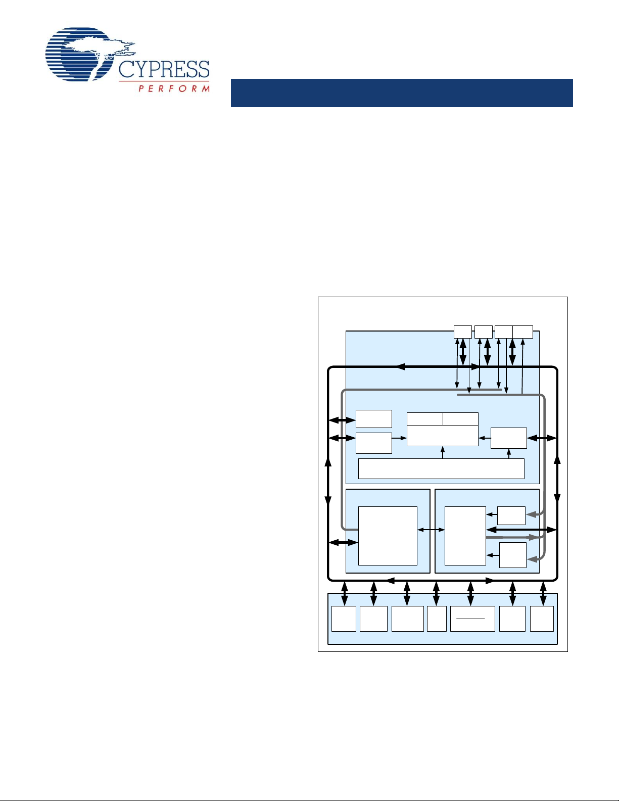
Logic Block Diagram
■ Powerful Harvard Architecture Processor
❐ M8C Processor Speeds to 24 MHz
❐ 8x8 Multiply, 32-Bit Accumulate
❐ Low Power at High Speed
❐ 3.0 to 5.25 V Operating Voltage
❐ Operating Voltages Down to 1.0V Using On-Chip Switch
Mode Pump (SMP)
❐ Industrial Temperature Range: -40°C to +85°C
■ Advanced Peripherals (PSoC Blocks)
❐ Six Rail-to-Rail Analog PSoC Blocks Provide:
• Up to 14-Bit ADCs
• Up to 8-Bit DACs
• Programmable Gain Amplifiers
• Programmable Filters and Comparators
❐ Four Digital PSoC Blocks Provide:
• 8 to 32-Bit Timers, Counters, and PWMs
• CRC and PRS Modules
• Full-Duplex UART
• Multiple SPI™ Masters or Slaves
• Connectable to all GPIO Pins
❐ Complex Peripherals by Combining Blocks
■ Precision, Programmable Clocking
❐ Internal ± 2.5% 24/48 MHz Oscillator
❐ High-Accuracy 24 MHz with Optional 32 kHz Crystal and PLL
❐ Optional External Oscillator, up to 24 MHz
❐ Internal Oscillator for Watchdog and Sleep
■ Flexible On-Chip Memory
❐ 4K Bytes Flash Program Storage 50,000 Erase/Write Cycles
❐ 256 Bytes SRAM Data Storage
❐ In-System Serial Programming (ISSP™)
❐ Partial Flash Updates
❐ Flexible Protection Modes
❐ EEPROM Emulation in Flash
■ Programmable Pin Configurations
❐ 25 mA Sink on all GPIO
❐ Pull up, Pull down, High Z, Strong, or Open Drain Drive
Modes on all GPIO
❐ Up to 10 Analog Inputs on GPIO
❐ Two 30 mA Analog Outputs on GPIO
❐ Configurable Interrupt on all GPIO
■ Additional System Resources
2
❐ I
C™ Slave, Master, and Multi-Master to 400 kHz
❐ Watchdog and Sleep Timers
❐ User-Configurable Low Voltage Detection
❐ Integrated Supervisory Circuit
❐ On-Chip Precision Voltage Reference
■ Complete Development Tools
❐ Free Development Software (PSoC Designer™)
❐ Full-Featured, In-Circuit Emulator and Programmer
❐ Full Speed Emulation
❐ Complex Breakpoint Structure
❐ 128K Bytes Trace Memory
Cypress Semiconductor Corporation • 198 Champion Court • San Jose, CA 95134-1709 • 408-943-2600
Document Number: 38-12011 Rev. *G Revised December 11, 2008
[+] Feedback
Page 2
CY8C24123
CY8C24223, CY8C24423
PSoC® Functional Overview
DIGITAL SYSTEM
To System Bus
D
i
g
i
t
a
l
C
l
o
c
k
s
F
r
o
m
C
o
r
e
Digital PSoC Block Array
To Analog
System
8
Row Input
Configuration
Row Output
Configuration
88
8
Row 0
DBB00 DBB01 DCB02 DCB03
4
4
GIE[7:0]
GIO[7:0]
GOE[7:0]
GOO[7:0]
Global Digital
Interconnect
Port 2 Port 1 Port 0
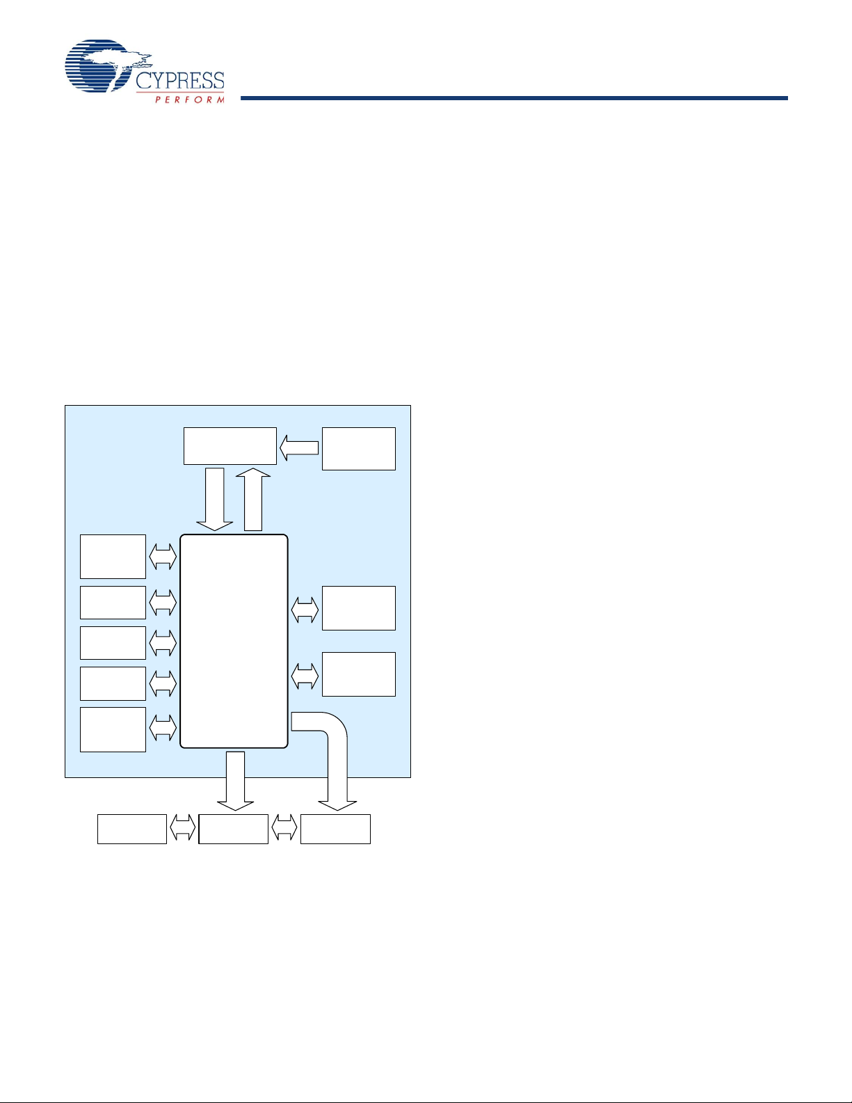
The PSoC® family consists of many Mixed Signal Array with
On-Chip Controller devices. These devices are designed to
replace multiple traditional MCU-based system components with
one, low cost single-chip programmable device. PSoC devices
include configurable blocks of analog and digital logic, and
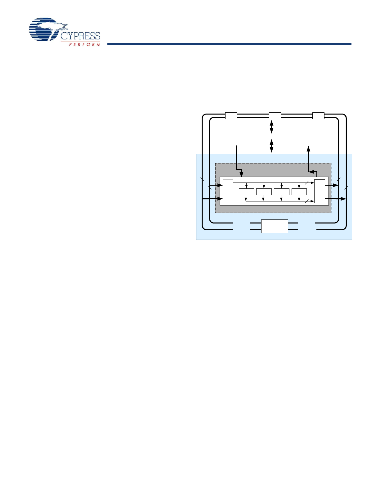
Digital System
The Digital System is composed of four digital PSoC blocks.
Each block is an 8-bit resource that can be used alone or
combined with other blocks to form 8, 16, 24, and 32-bit
peripherals, which are called user module references.
Figure 1. Digital System Block Diagram
programmable interconnects. This architecture allows the user
to create customized peripheral configurations that match the
requirements of each individual application. Additionally, a fast
CPU, Flash program memory, SRAM data memory, and configurable IO are included in a range of convenient pinouts and
packages.
The PSoC architecture, as shown in the Logic Block Diagram on
page 1, is comprised of four main areas: PSoC Core, Digital
System, Analog System, and System Resources. Configurable
global busing allows all the device resources to be combined into
a complete custom system. The PSoC CY8C24x23 family can
have up to three IO ports that connect to the global digital and
analog interconnects, providing access to four digital blocks and
6 analog blocks.
PSoC Core
The PSoC Core is a powerful engine that supports a rich feature
set. The core includes a CPU, memory , clocks, and configurable
GPIO (General Purpose IO).
The M8C CPU core is a powerful processor with speeds up to
24 MHz, providing a four MIPS 8-bit Harvard architecture
microprocessor. The CPU uses an interrupt controller with 11
vectors, to simplify programming of real time embedded events.
Program execution is timed and protected using the included
Sleep and Watch Dog Timers (WDT).
Memory encompasses 4 KB of Flash for program storage, 256
bytes of SRAM for data storage, and up to 2 KB of EEPROM
emulated using the Flash. Program Flash uses four protection
levels on blocks of 64 bytes, allowing customized software IP
protection.
The PSoC device incorporates flexible internal clock generators,
including a 24 MHz IMO (internal main oscillator) accurate to
2.5% over temperature and voltage. The 24 MHz IMO can also
be doubled to 48 MHz for use by the digital system. A low power
32 kHz ILO (internal low speed oscillator) is provided for the
Sleep timer and WDT. If crystal accuracy is desired, the ECO
(32.768 kHz external crystal oscillator) is available for use as a
Real Time Clock (RTC) and can optionally generate a
crystal-accurate 24 MHz system clock using a PLL. The clocks,
together with programmable clock dividers (as a System
Resource), provide the flexibility to integrate almost any timing
requirement into the PSoC device.
PSoC GPIOs provide connection to the CPU, digital and analog
resources of the device. Each pin’s drive mode may be selected
from eight options, allowing great flexibility in external interfacing. Every pin also has the capability to generate a system
interrupt on high level, low level, and change from last read.
Digital peripheral configurations include:
■ PWMs (8 to 32 bit)
■ PWMs with Dead band (8 to 32 bit)
■ Counters (8 to 32 bit)
■ Timers (8 to 32 bit)
■ UART 8-bit with selectable parity (up to one)
■ SPI master and slave (up to one)
■ I2C slave and master (one available as a System Resource)
■ Cyclical Redundancy Checker/Generator (8 to 32 bit)
■ IrDA (up to one)
■ Pseudo Random Sequence Generators (8 to 32 bit)
The digital blocks can be connected to any GPIO through a
series of global buses that can route any signal to any pin. The
buses also allow for signal multiplexing and for performing logic
operations. This configurability frees your designs from the
constraints of a fixed peripheral controller.
Digital blocks are provided in rows of four, where the number of
blocks varies by PSoC device family. This allows the optimum
choice of system resources for your application. Family
resources are listed in the table PSoC Device Characteristics on
page 4.
Document Number: 38-12011 Rev. *G Page 2 of 43
[+] Feedback
Page 3
CY8C24123
CY8C24223, CY8C24423
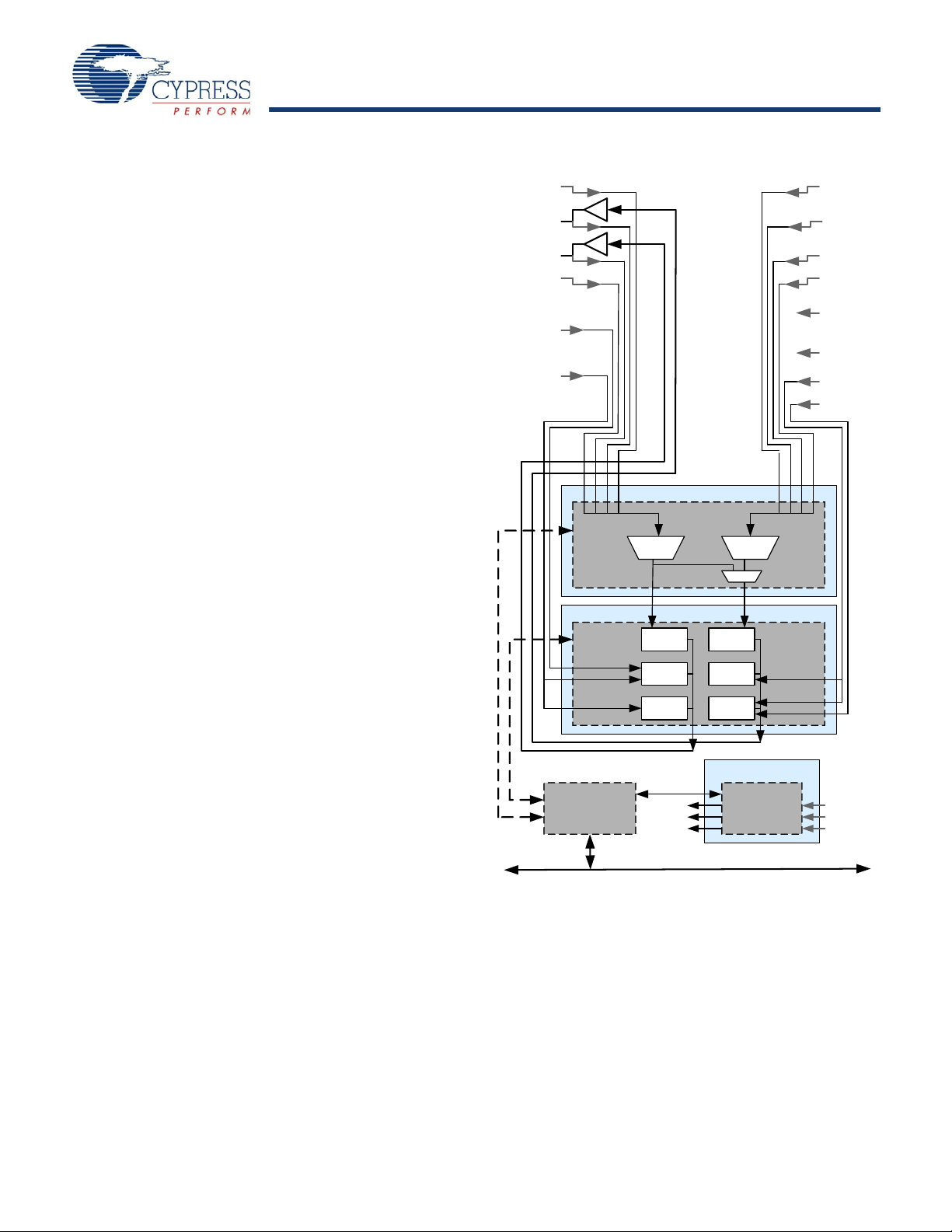
Analog System
ACB00 ACB01
Block Array
Array Input Configuration
ACI1[1:0]
ASD20
ACI0[1:0]
P0[6]
P0[4]
P0[2]
P0[0]
P2[2]
P2[0]
P2[6]
P2[4]
RefIn
AGNDIn
P0[7]
P0[5]
P0[3]
P0[1]
P2[3]
P2[1]
Reference
Generators
AGNDIn
RefIn
Bandgap
RefHi
RefLo
AGND
ASD11
ASC21
ASC10
Interface to
Digital System
M8C Interface (Address Bus, Data Bus, Etc.)
Analog Reference
The Analog System is composed of six configurable blocks, each
comprised of an opamp circuit allowing the creation of complex
analog signal flows. Analog peripherals are very flexible and can
be customized to support specific application requirements.
Some of the more common PSoC analog functions (most
available as user modules) are:
■ Analog-to-digital converters (up to two, with 6 to 14-bit
resolution, selectable as Incremental, Delta Sigma, and SAR)
■ Filters (two and four pole band-pass, low-pass, and notch)
■ Amplifiers (up to two, with selectable gain to 48x)
■ Instrumentation amplifiers (one with selectable gain to 93x)
■ Comparators (up to two, with 16 selectable thresholds)
■ DACs (up to two, with 6 to 9-bit resolution)
■ Multiplying DACs (up to two, with 6- to 9-bit resoluti on)
■ High current output drivers (two with 30 mA drive as a Core
Resource)
■ 1.3V reference (as a System Resource)
■ DTMF dialer
■ Modulators
■ Correlators
■ Peak detectors
■ Many other topologies possible
Analog blocks are provided in columns of three, which includes
one CT (Continuous Time) and two SC (Switched Capacitor)
blocks. The number of blocks is dependant on the device family
which is detailed in the table PSoC Device Characteristics on
page 4.
Figure 2. Analog System Block Diagram
Document Number: 38-12011 Rev. *G Page 3 of 43
[+] Feedback
Page 4
CY8C24123
CY8C24223, CY8C24423
Additional System Resources
System Resources, some of which have been previously listed,
provide additional capability useful to complete systems.
Additional resources include a multiplier, decimator, switch mode
pump, low voltage detection, and power on reset. Brief statements describing the merits of each system resource follow:
■ Digital clock dividers provide three customizable clock
frequencies for use in applications. The clocks can be routed
to both the digital and analog systems. Additional clocks can
be generated using digital PSoC blocks as clock dividers.
■ A multiply accumulate (MAC) provides a fast 8-bit multiplier
with 32-bit accumulate, to assist in both general math and
digital filters.
■ The decimator provides a custom hardware filter for digital
signal processing applications including the creation of Delta
Sigma ADCs.
■ The I2C module provides 100 and 400 kHz communication over
two wires. Slave, master, and multi-master modes are all
supported.
■ Low Voltage Detection (LVD) interrupts can signal the appli-
cation of falling voltage levels, while the advanced POR (Power
On Reset) circuit eliminates the need for a system supervisor.
■ An internal 1.3V reference provides an absolute reference for
the analog system, including ADCs and DACs.
■ An integrated switch mode pump (SMP) generates normal
operating voltages from a single 1.2V battery cell, providing a
low cost boost converter.
PSoC Device Characteristics
Depending on your PSoC device characteristics, the digital and
analog systems can have 16, 8, or 4 digital blocks and 12, 6, or
3 analog blocks. The following table lists the resources available
for specific PSoC device groups.
Table 1. PSoC Device Characteristics
PSoC Part
Number
CY8C29x66 up to 644 16 12 4 4 12
CY8C27x66
CY8C27x43
IO
Digital
Rows
Digital
Digital
up to 442 8 12 4 4 12
up to 442 8 12 4 4 12
Blocks
Inputs
Analog
Analog
Outputs
Analog
Columns
Analog
Getting Started
The quickest path to understanding the PSoC silicon is by
reading this data sheet and using the PSoC Designer Integrated
Development Environment (IDE). This data sheet is an overview
of the PSoC integrated circuit and presents specific pin, register,
and electrical specifications. For in-depth information, along with
detailed programming information, refer the PSoC Programmable Sytem-on-Chip Technical Reference Manual.
For up-to-date Ordering, Packaging, and Electrical Specification
information, refer the latest PSoC device data sheets on the web
at http://www.cypress.com/psoc.
Development Kits
Development Kits are available from the following distributors:
Digi-Key, Avnet, Arrow, and Future. The Cypress Online Store
contains development kits, C compilers, and all accessories for
PSoC development. Go to the Cypress Online Store web site at
http://www.cypress.com, click the Online Store shopping cart
icon at the bottom of the web page, and click PSoC (Program-
mable System-on-Chip) to view a current list of available items.
Technical Training
Free PSoC technical training is available for beginners and is
taught by a marketing or application engineer over the phone.
PSoC training classes cover designing, debugging, advanced
analog, and application-specific classes covering topics, such as
PSoC and the LIN bus. Go to http://www.cypress.com, click on
Design Support located on the left side of the web page, and
select Technical Training for more details.
Consultants
Certified PSoC Consultants offer everything from technical
assistance to completed PSoC designs. To contact or become a
PSoC Consultant go to http://www.cypress.com, click on Design
Support located on the left side of the web page, and select
CYPros Consultants.
Technical Support
PSoC application engineers take pride in fast and accurate
response. They can be reached with a 4-hour guaranteed
response at http://www.cypress.com/support.
Blocks
Application Notes
A long list of application notes can assist you in every aspect of
your design effort. To view the PSoC application notes, go to the
http://www.cypress.com web site and select Application Notes
under the Design Resources list located in the center of the web
page. Application notes are listed by date as default.
CY8C24x23 up to 241 4 12 2 2 6
CY8C22x13
Document Number: 38-12011 Rev. *G Page 4 of 43
up to 161 4 8 1 1 3
[+] Feedback
Page 5
CY8C24123
CY8C24223, CY8C24423
Development Tools
Commands
Results
PSoC
TM
Designer
Core
Engine
PSoC
Configuration
Sheet
Manufacturing
Information
File
Device
Database
Importable
Design
Database
Device
Programmer
Graphical Designer
Interface
Context
Sensitive
Help
Emulation
Pod
In-Circuit
Emulator
Project
Database
Application
Database
User
Modules
Library
PSoCTM
Designer
The Cypress MicroSystems PSoC Designer is a Microsoft
Windows-based, integrated development environment for the
Programmable System-on-Chip (PSoC) devices. The PSoC
Designer IDE and application runs on Windows 98, Windows NT
4.0, Windows 2000, Windows Millennium (Me), or Windows XP
(refer Figure 3).
PSoC Designer helps the customer to select an operating
configuration for the PSoC, write application code that uses the
PSoC, and debug the application. This system provides design
database management by project, an integrated debugger with
In-Circuit Emulator, in-system programming support, and the
CYASM macro assembler for the CPUs.
PSoC Designer also supports a high-level C language compiler
developed specifically for the devices in the family.
Figure 3. PSoC Designer Subsystems
PSoC Designer Software Subsystems
®
Device Editor
The Device Editor subsystem allows the user to select different
onboard analog and digital components called user modules
using the PSoC blocks. Examples of user modules are ADCs,
DACs, Amplifiers, and Filters.
The device editor also supports easy development of multiple
configurations and dynamic reconfiguration. Dynamic
configuration allows for changing configurations at run time.
PSoC Designer sets up power on initialization tables for selected
PSoC block configurations and creates source code for an
application framework. The framework contains software to
operate the selected components and, if the project uses more
than one operating configuration, contains routines to switch
between different sets of PSoC block configurations at run time.
PSoC Designer can print out a configuration sheet for a given
project configuration for use during application programming in
conjunction with the Device Data Sheet. After the framework is
generated, the user can add application-specific code to flesh
out the framework. It is also possible to change the selected
components and regenerate the framework.
Design Browser
The Design Browser allows users to select and imp ort preconfigured designs into the user’s project. Users can easily browse
a catalog of preconfigured designs to facilitate time-to-design.
Examples provided in the tools include a 300-baud modem, LIN
Bus master and slave, fan controller, and magnetic card reader.
Application Editor
In the Application Editor you can edit your C language and
Assembly language source code. You can also assemble,
compile, link, and build.
Assembler. The macro assembler allows the assembly code to
be merged seamlessly with C code. The link libraries automatically use absolute addressing or can be compiled in relative
mode, and linked with other software modules to get absolute
addressing.
C Language Compiler. A C language compiler is available that
supports Cypress MicroSystems’ PSoC family devices. Even if
you have never worked in the C language before, the product
quickly allows you to create complete C programs for the PSoC
family devices.
The embedded, optimizing C compiler provides all th e features
of C tailored to the PSoC architecture. It comes complete with
embedded libraries providing port and bus operations, standard
keypad and display support, and extended math functionality.
Document Number: 38-12011 Rev. *G Page 5 of 43
[+] Feedback
Page 6
CY8C24123
CY8C24223, CY8C24423
Debugger
The PSoC Designer Debugger subsystem provides hardware
in-circuit emulation, allowing the designer to test the program in
a physical system while providing an internal view of the PSoC
device. Debugger commands allow the designer to read and
program and read and write data memory, read and write IO
registers, read and write CPU registers, set and clear breakpoints, and provide program run, halt, and step control. The
debugger also allows the designer to create a trace buffer of
registers and memory locations of interest.
Online Help System
The online help system displays online, context-sensitive help
for the user. Designed for procedural and quick reference, each
functional subsystem has its own context-sensitive help. This
system also provides tutorials and links to FAQs and an Online
Support Forum to aid the designer in getting started.
Hardware Tools
In-Circuit Emulator
A low cost, high functionality ICE (In-Circuit Emulator) is
available for development support. This hardware has the
capability to program single devices.
The emulator consists of a base unit that connects to the PC by
way of the parallel or USB port. The base unit is universal and
operates with all PSoC devices. Emulation pods for each device
family are available separately. The emulation pod takes the
place of the PSoC device in the target board and performs full
speed (24 MHz) operation.
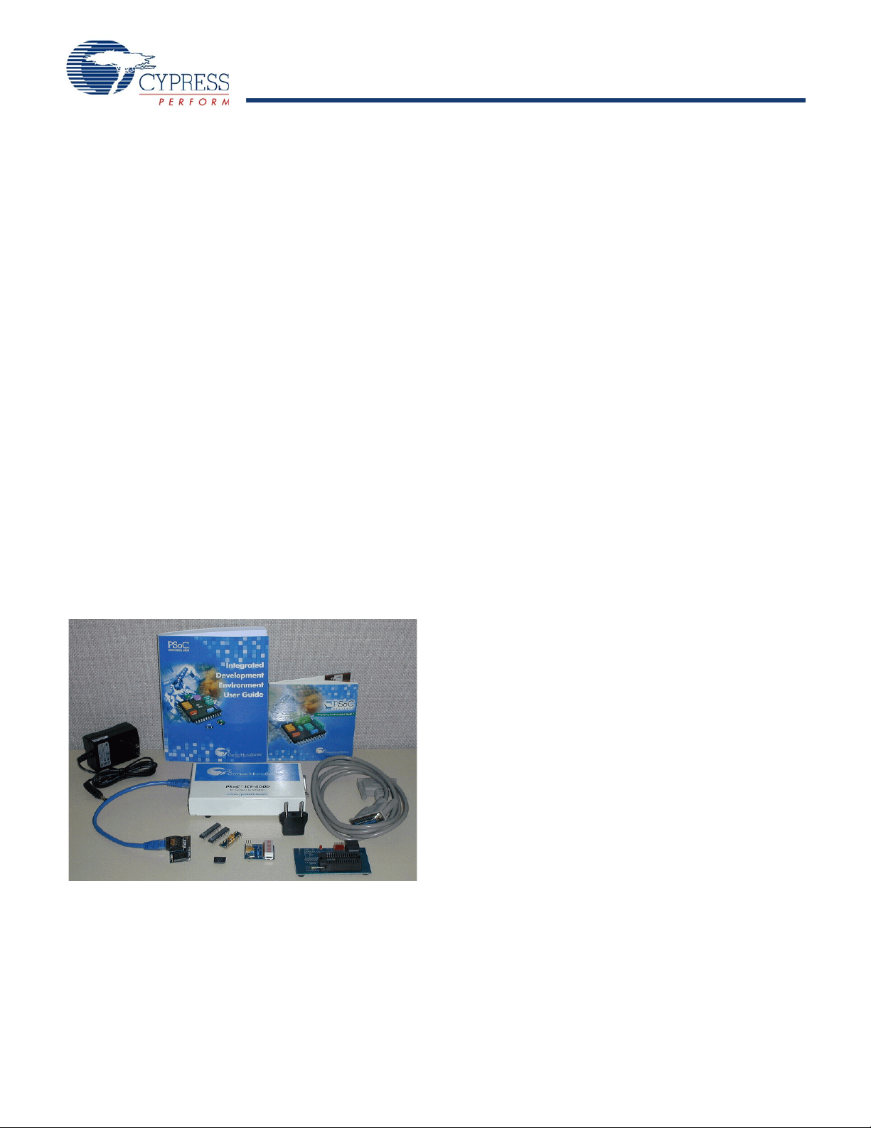
Figure 4. PSoC Development Tool Kit
User Modules and the PSoC Development Process
The development process for the PSoC device differs from that
of a traditional fixed function microprocessor. The configurable
analog and digital hardware blocks give the PSoC architecture a
unique flexibility that pays dividends in managing specification
change during development and by lowering inventory costs.
These configurable resources, called PSoC Blocks, have the
ability to implement a wide variety of user-selectable functions.
Each block has several registers that determine its function and
connectivity to other blocks, multiplexers, buses and to the IO
pins. Iterative development cycles permit you to adapt the
hardware as well as the software. This substantially lowers the
risk of having to select a different part to meet the final design
requirements.
To speed the development process, the PSoC Designer
Integrated Development Environment (IDE) provides a library of
pre-built, pre-tested hardware peripheral functions, called “User
Modules.” User modules make selecting and implementing
peripheral devices simple, and come in analog, digital, and
mixed signal varieties. The standard User Module library
contains over 50 common peripherals such as ADCs, DACs
Timers, Counters, UARTs, and other not-so common peripherals
such as DTMF Generators and Bi-Quad analog filter sections.
Each user module establishes the basic register settings that
implement the selected function. It also provides parameters that
allow you to tailor its precise configuration to your particular
application. For example, a Pulse Width Modulator User Module
configures one or more digital PSoC blocks, one for each 8 bits
of resolution. The user module parameters permit you to
establish the pulse width and duty cycle. User modules also
provide tested software to cut your development time. The user
module application programming interface (API) provides
high-level functions to control and respond to hardware events
at run-time. The API also provides optional interrupt service
routines that you can adapt as needed.
The API functions are documented in user module data sheets
that are viewed directly in the PSoC Designer IDE. These data
sheets explain the internal operation of the user module and
provide performance specifications. Each data sheet describes
the use of each user module parameter and documents the
setting of each register controlled by the user module.
The development process starts when you open a new project
and bring up the Device Editor, a pictorial environment (GUI) for
configuring the hardware. You pick the user modules you need
for your project and map them onto the PSoC blocks with
point-and-click simplicity. Next, you build signal chains by interconnecting user modules to each other and the IO pins. At this
stage, you also configure the clock source connections and enter
parameter values directly or by selecting values from drop-down
menus. When you are ready to test the hardware configuration
or move on to developing code for the project, you perform the
“Generate Application” step. This causes PSoC Designer to
generate source code that automatically configures the device to
your specification and provides the high-level user module API
functions.
Document Number: 38-12011 Rev. *G Page 6 of 43
[+] Feedback
Page 7
CY8C24123
CY8C24223, CY8C24423
Figure 5. User Module and Source Code Development Flows
Debugger
Interface
to ICE
Application Editor
Device Editor
Project
Manager
Source
Code
Editor
Storage
Inspector
User
Module
Selection
Placement
and
Parameter
-ization
Generate
Application
Build
All
Event &
Breakpoint
Manager
Build
Manager
Source
Code
Generator
The next step is to write your main program, and any
sub-routines using PSoC Designer’s Application Editor
subsystem. The Application Editor includes a Project Manager
that allows you to open the project source code files (includ ing
all generated code files) from a hierarchal view. The source code
editor provides syntax coloring and advanced edit features for
both C and assembly language. File search capabilities include
simple string searches and recursive “grep-style” patterns. A
single mouse click invokes the Build Manager. It employs a
professional-strength “makefile” system to automatically analyze
all file dependencies and run the compiler and assembler as
necessary. Project-level options control optimization strategies
used by the compiler and linker. Syntax errors are displayed in a
console window. Double clicking the error message takes you
directly to the offending line of source code. When all is correct,
the linker builds a ROM file image suitable for programming.
The last step in the development process takes place inside the
PSoC Designer’s Debugger subsystem. The Debugger
downloads the ROM image to the In-Circuit Emulator (ICE)
where it runs at full speed. Debugger capabilities rival those of
systems costing many times more. In addition to traditional
single-step, run-to-breakpoint and watch-variable features, the
Debugger provides a large trace buffer and allows you define
complex breakpoint events that include monitoring address and
data bus values, memory locations and external signals.
Document Conventions
Acronyms Used
The following table lists the acronyms that are used in this
document.
Table 2. Acronyms
Acronym Description
AC alternating current
ADC analog-to-digital converter
API application programming interface
CPU central processing unit
CT continuous time
DAC digital-to-analog converter
DC direct current
EEPROM el ectrically erasable programmable read-only
memory
FSR full scale range
GPIO general purpose IO
IO input/output
IPOR imprecise power on reset
LSb least-significant bit
LVD low voltage detect
MSb most-significant bit
PC program counter
POR power on reset
PPOR precision power on reset
®
PSoC
PWM pulse width modulator
RAM random access memory
ROM read only memory
SC switched capacitor
SMP switch mode pump
Units of Measure
A units of measure table is located in the Electrical Specifications
section. Table 7 on page 11 lists all the abbreviations used to
measure the PSoC devices.
Numeric Naming
Hexadecimal numbers are represented with all letters in
uppercase with an appended lowercase ‘h’ (for example, ‘14h’ or
‘3Ah’). Hexadecimal numbers may also be represented by a ‘0x’
prefix, the C coding convention. Binary numbers have an
appended lowercase ‘b’ (for example, 01010100b’ or
‘01000011b’). Numbers not indicated by an ‘h’ or ‘b’ are decimal.
Programmable System-on-Chip
Document Number: 38-12011 Rev. *G Page 7 of 43
[+] Feedback
Page 8
CY8C24123
CY8C24223, CY8C24423
Pinouts
PDIP
SOIC
1
2
3
4
8
7
6
5
Vdd
P0[4], AI
P0[2], AI
P1[0], XTALout, I2C SDA
AIO, P0[5]
AIO, P0[3]
I2C SCL, XTALin, P1[1]
Vss
AI, P0[7]
AIO, P0[5]
AIO, P0[3]
AI, P0[1]
SMP
I2C SCL, P1[7]
I2C SDA, P1[5]
P1[3]
I2C SCL, XTALin, P1[1]
Vss
PDIP
SSOP
SOIC
20
19
18
17
16
15
14
13
12
11
1
2
3
4
5
6
7
8
9
10
Vdd
P0[6], AI
P0[4], AI
P0[2], AI
P0[0], AI
XRES
P1[6]
P1[4], EXTCLK
P1[2]
P1[0], XTALout, I2C SDA
The CY8C24x23 PSoC device is available in a variety of packages which are listed and illustrated in the following tables. Every port
pin (labeled with a “P”) is capable of Digital IO. However, Vss, Vdd, SMP, and XRES are not capable of Digital IO.
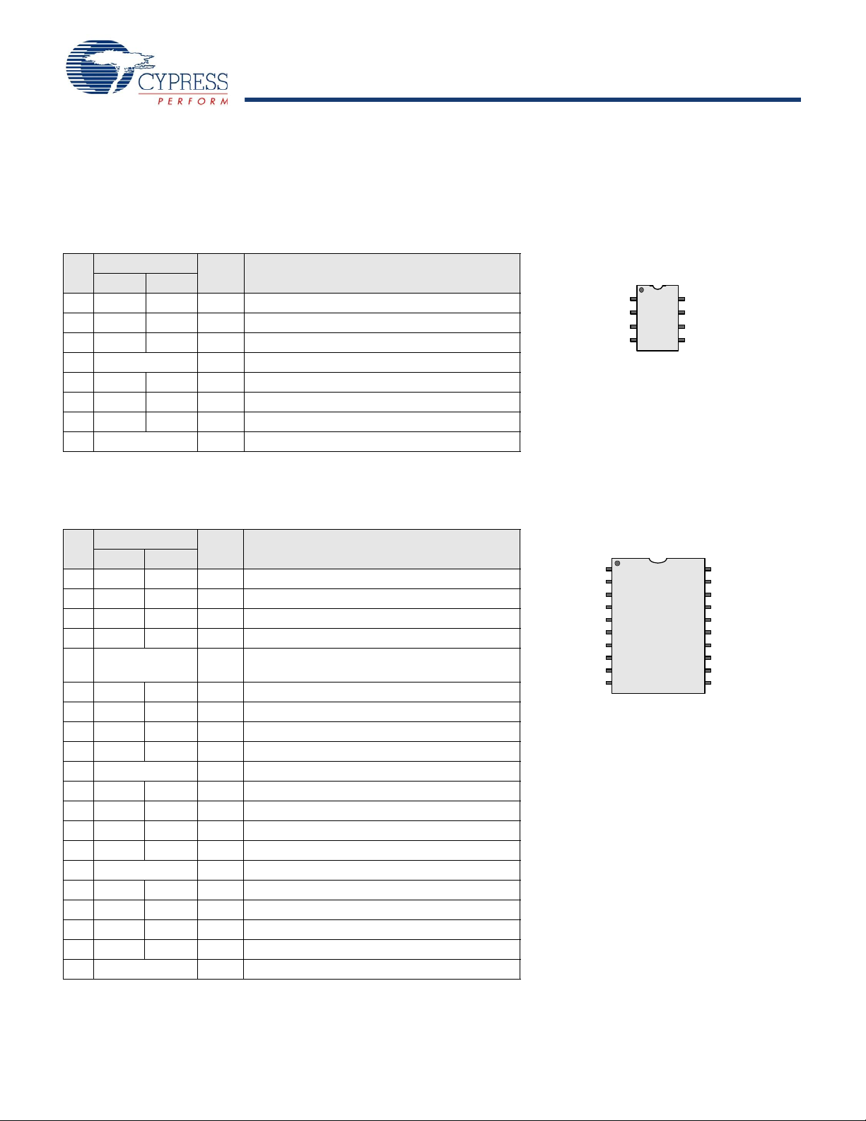
8-Pin Part Pinout
Table 3. 8-Pin Part Pinout (PDIP, SOIC)
Pin
No.
1 IO IO P0[5] Analog column mux input and column output
2 IO IO P0[3] Analog column mux input and column output
3 IO P1[1] Crystal Input (XTALin), I2C Serial Clock (SCL)
4 Power Vss Ground connection
5 IO P1[0] Crystal Output (XT ALout), I2C Serial Data (SDA)
6 IO I P0[2] Analog column mux input
7 IO I P0[4] Analog column mux input
8 Power Vdd Supply voltage
LEGEND: A = Analog, I = Input, and O = Output.
20-Pin Part Pinout
Table 4. 20-Pin Part Pinout (PDIP, SSOP, SOIC)
Pin
No.
1 IO I P0[7] Analog column mux input
2 IO IO P0[5] Analog column mux input and column output
3 IO IO P0[3] Analog column mux input and column output
4 IO I P0[1] Analog column mux input
5 Power SMP Switch Mode Pump (SMP) connection to external
6 IO P1[7] I2C Serial Clock (SCL
7 IO P1[5] I2C Serial Data (SDA)
8 IO P1[3]
9 IO P1[1] Crystal Input (XTALin), I2C Serial Clock (SCL)
10 Power Vss Ground connection
11 IO P1[0] Crystal Output (XT ALout), I2C Serial Data (SDA)
12 IO P1[2]
13 IO P1[4] Optional External Clock Input (EXTCLK)
14 IO P1[6]
15 Input XRES Active high external reset with internal pull down
16 IO I P0[0] Analog column mux input
17 IO I P0[2] Analog column mux input
18 IO I P0[4] Analog column mux input
19 IO I P0[6] Analog column mux input
20 Power Vdd Supply voltage
LEGEND: A = Analog, I = Input, and O = Output.
Document Number: 38-12011 Rev. *G Page 8 of 43
Type
Digital Analog
Type
Digital Analog
Pin
Name
Pin
Name
components required
Description
Description
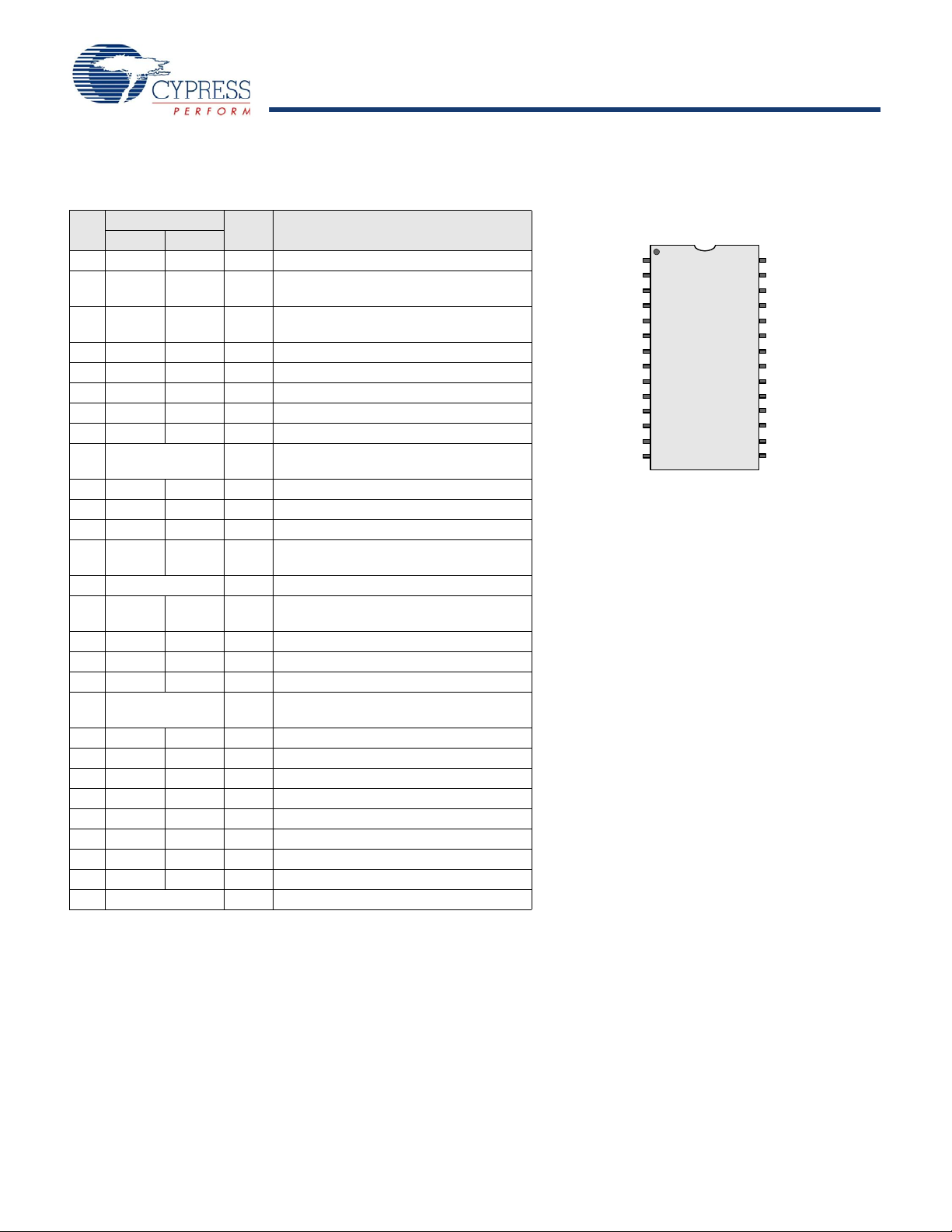
Figure 6. CY8C24123 8-Pin PSoC Device
Figure 7. CY8C24223 20-Pin PSoC Device
[+] Feedback
Page 9
CY8C24123
CY8C24223, CY8C24423
28-Pin Part Pinout
AI, P0[7]
AIO, P0[5]
AIO, P0[3]
AI, P0[1]
P2[7]
P2[5]
AI, P2[3]
AI, P2[1]
SMP
I2C SCL, P1[7]
I2C SDA, P1[5]
P1[3]
I2C SCL, XTALin, P1[1]
Vss
Vdd
P0[6], AI
P0[4], AI
P0[2], AI
P0[0], AI
P2[6], External VRef
P2[4], External AGND
P2[2], AI
P2[0], AI
XRES
P1[6]
P1[4], EXTCLK
P1[2]
P1[0], XTALout, I2C SDA
PDIP
SSOP
SOIC
1
2
3
4
5
6
7
8
9
10
11
12
13
14
28
27
26
25
24
23
22
21
20
19
18
17
16
15
Table 5. 28-Pin Part Pinout (PDIP, SSOP, SOIC)
Pin
No.
1 IO I P0[7] Analog column mux input
2 IO IO P0[5] Analog column mux input and column
3 IO IO P0[3] Analog column mux input and column
4 IO I P0[1] Analog column mux input.
5 IO P2[7]
6 IO P2[5]
7 IO I P2[3] Direct switched capacitor block input
8 IO I P2[1] Direct switched capacitor block input
9 Power SMP Switch Mode Pump (SMP) connection to
10 IO P1[7] I2C Serial Clock (SCL)
11 IO P1[5] I2C Serial Data (SDA)
12 IO P1[3]
13 IO P1[1] Crystal Input (XTALin), I2C Serial Clock
14 Power Vss Ground connection
15 IO P1[0] Crystal Output (XTALout), I2C Serial
16 IO P1[2]
17 IO P1[4] Optional External Clock Input (EXTCLK)
18 IO P1[6]
19 Input XRES Active high external reset with internal
20 IO I P2[0] Direct switched capacitor block input
21 IO I P2[2] Direct switched capacitor block input
22 IO P2[4] External Analog Ground (AGND)
23 IO P2[6] External Voltage Reference (VRef)
24 IO I P0[0] Analog column mux input
25 IO I P0[2] Analog column mux input
26 IO I P0[4] Analog column mux input
27 IO I P0[6] Analog column mux input
28 Power Vdd Supply voltage
Type
Digital Analog
Pin
Name
Description
output
output
external components required
(SCL)
Data (SDA)
pull down
Figure 8. CY8C24423 28-Pin PSoC Device
LEGEND: A = Analog, I = Input, and O = Output.
Document Number: 38-12011 Rev. *G Page 9 of 43
[+] Feedback
Page 10
CY8C24123
CY8C24223, CY8C24423
P2[7]
P2[5]
AI, P2[3]
AI, P2[1]
Vss
SMP
MLF
(Top View)
9
101112
131415
16
1
2
3
4
5
6
7
8
24
23
22
21
20
19
18
17
32313029282726
25
P0[1], AI
P0[3], AIO
P0[5], AIO
P0[7], AI
Vdd
P0[6], AI
P0[4], AI
NC
I2C SCL, P1[7]
I2C SDA, P1[5]
P0[2], AI
P0[0], AI
XRES
P1[6]
NC
P1[3]
I2C SCL, XTALin, P1[1]
Vss
I2C SDA, XTALout, P1[0]
P1[2]
EXTCLK, P1[4]
NC
P2[6], External VRef
P2[4], External AGND
P2[2], AI
P2[0], AI
32-Pin Part Pinout
Table 6. 32-Pin Part Pinout (MLF*)
Pin
No.
1 IO P2[7]
2 IO P2[5]
3 IO I P2[3] Direct switched cap acitor block input
4 IO I P2[1] Direct switched cap acitor block input
5 Power Vss Ground connection
6 Power SMP Switch Mode Pump (SMP)
7 IO P1[7] I2C Serial Clock (SCL)
8 IO P1[5] I2C Serial Data (SDA)
9 NC No connection. Do not use.
10 IO P1[3]
11 IO P1[1] Crystal Input (XTALin), I2C Serial
12 Power Vss Ground connection
13 IO P1[0] Crystal Output (XTALout), I2C Serial
14 IO P1[2]
15 IO P1[4 ] Optional External Clock Input
16 NC No connection. Do not use.
17 IO P1[6]
18 Input XRES Active high external reset with
19 IO I P2[0] Direct switched capacitor block input
20 IO I P2[2] Direct switched capacitor block input
21 IO P2[4] External Analog Ground (AGND)
22 IO P2[6] External Voltage Reference (VRef)
23 IO I P0[0] Analog column mux input
24 IO I P0[2] Analog column mux input
25 NC No connection. Do not use.
26 IO I P0[4] Analog column mux input
27 IO I P0[6] Analog column mux input
28 Power Vdd Supply voltage
29 IO I P0[7] Analog column mux input
30 IO IO P0[5] Analog column mux input and
31 IO IO P0[3] Analog column mux input and
32 IO I P0[1] Analog column mux input
LEGEND: A = Analog, I = Input, and O = Output.
* The MLF package has a center pad that must be connected to the same ground as the
Vss pin.
Type
Digital Analog
Pin
Name
Description
connection to external components
required
Clock (SCL)
Data (SDA)
(EXTCLK)
internal pull down
column output
column output
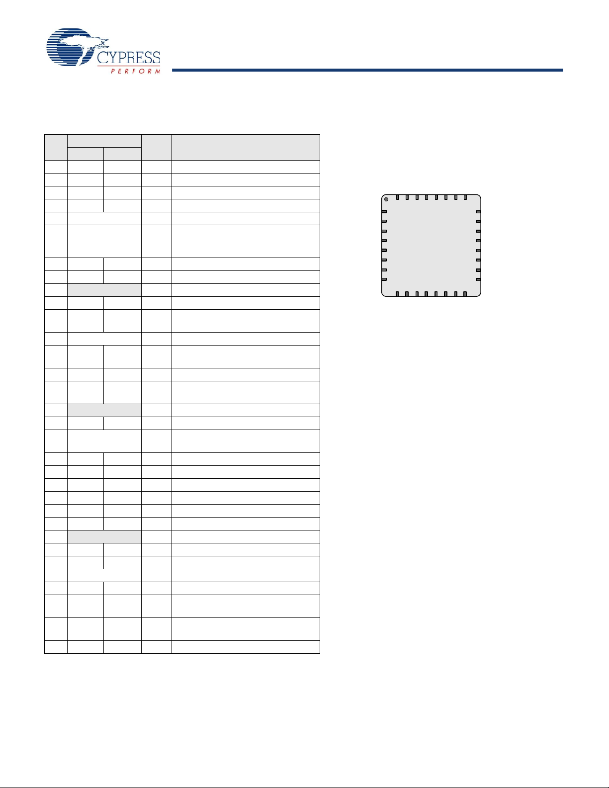
Figure 9. CY8C24423 32-Pin PSoC Device
Document Number: 38-12011 Rev. *G Page 10 of 43
[+] Feedback
Page 11
CY8C24123
CY8C24223, CY8C24423
Register Reference
This section lists the registers of the CY8C27xxx PSoC device
by way of mapping tables, in offset order. For detailed register
information, reference the PSoC Programmable
System-on-Chip Technical Reference Manual.
Register Conventions
Abbreviations Used
The register conventions specific to this section are listed in the
following table.
Table 7. Abbreviations
Convention Description
RW Read and write register or bit(s)
R Read register or bit(s)
W Write register or bit(s)
L Logical register or bit(s)
C Clearable register or bit(s)
# Access is bit specific
Register Mapping Tables
The PSoC device has a total register address space of 512
bytes. The register space is also referred to as IO space and is
broken into two parts. The XOI bit in the Flag register determines
which bank the user is currently in. When the XOI bi t is set, the
user is said to be in the “extended” address space or the “configuration” registers.
Note In the following register mapping tables, blank fields are
Reserved and must not be accessed.
Document Number: 38-12011 Rev. *G Page 11 of 43
[+] Feedback
Page 12
CY8C24123
CY8C24223, CY8C24423
Table 8. Register Map Bank 0 Table: User Space
PRT0DR 00 RW 40 ASC10CR0 80 RW C0
Name
PRT0IE 01 RW 41 ASC10CR1 81 RW C1
PRT0GS 02 RW 42 ASC10CR2 82 RW C2
PRT0DM2 03 RW 43 ASC10CR3 83 RW C3
PRT1DR 04 RW 44 ASD11CR0 84 RW C4
PRT1IE 05 RW 45 ASD11CR1 85 RW C5
PRT1GS 06 RW 46 ASD11CR2 86 RW C6
PRT1DM2 07 RW 47 ASD11CR3 87 RW C7
PRT2DR 08 RW 48 88 C8
PRT2IE 09 RW 49 89 C9
PRT2GS 0A RW 4A 8A CA
PRT2DM2 0B RW 4B 8B CB
DBB00DR0 20 # AMX_IN 60 R W A0 INT_MSK0 E0 RW
DBB00DR1 21 W 61 A1 INT_MSK1 E1 RW
DBB00DR2 22 RW 62 A2 INT_VC E2 RC
DBB00CR0 23 # ARF_CR 63 RW A3 RES_WDT E3 W
DBB01DR0 24 # CMP_CR0 64 # A4 DEC_DH E4 RC
DBB01DR1 25 W ASY_CR 65 # A5 DEC_DL E5 RC
DBB01DR2 26 RW CMP_CR1 66 RW A6 DEC_CR0 E6 RW
DBB01CR0 27 # 67 A7 DEC_CR1 E7 RW
DCB02DR0 28 # 68 A8 MUL_X E8 W
DCB02DR1 29 W 69 A9 MUL_Y E9 W
DCB02DR2 2A RW 6A AA MUL_DH EA R
DCB02CR0 2B # 6B AB MUL_DL EB R
DCB03DR0 2C # 6C AC ACC_DR1 EC RW
DCB03DR1 2D W 6D AD ACC_DR0 ED RW
Blank fields are Reserved and must not be accessed. # Access is bit specific.
Addr
(0,Hex)
Access
0C 4C 8C CC
0D 4D 8D CD
0E 4E 8E CE
0F 4F 8F CF
10 50 ASD20CR0 90 RW D0
11 51 ASD20CR1 91 RW D1
12 52 ASD20CR2 92 RW D2
13 53 ASD20CR3 93 RW D3
14 54 ASC21CR0 94 RW D4
15 55 ASC21CR1 95 RW D5
16 56 ASC21CR2 96 RW I2C_CFG D6 RW
17 57 ASC21CR3 97 RW I2C_SCR D7 #
18 58 98 I2C_DR D8 RW
19 59 99 I2C_MSCR D9 #
1A 5A 9A INT_CLR0 DA RW
1B 5B 9B INT_CLR1 DB RW
1C 5C 9C DC
1D 5D 9D INT_CLR3 DD RW
1E 5E 9E INT_MSK3 DE RW
1F 5F 9F DF
Name
Addr
(0,Hex)
Access
Name
Addr
(0,Hex)
Access
Name
Addr
(0,Hex)
Access
Document Number: 38-12011 Rev. *G Page 12 of 43
[+] Feedback
Page 13
CY8C24123
CY8C24223, CY8C24423
Table 8. Register Map Bank 0 Table: User Space (continued)
DCB03DR2 2E RW 6E AE ACC_DR3 EE RW
Name
DCB03CR0 2F # 6F AF ACC_DR2 EF RW
Blank fields are Reserved and must not be accessed. # Access is bit specific.
Addr
(0,Hex)
Access
30 ACB00CR3 70 RW RDI0RI B0 RW F0
31 ACB00CR0 71 RW RDI0SYN B1 RW F1
32 ACB00CR1 72 RW RDI0IS B2 RW F2
33 ACB00CR2 73 RW RDI0LT0 B3 RW F3
34 ACB01CR3 74 RW RDIOLT1 B4 RW F4
35 ACB01CR0 75 RW RDI0RO0 B5 RW F5
36 ACB01CR1 76 RW RDI0RO1 B6 RW F6
37 ACB01CR2 77 RW B7 CPU_F F7 RL
38 78 B8 F8
39 79 B9 F9
3A 7A BA FA
3B 7B BB FB
3C 7C BC FC
3D 7D BD FD
3E 7E BE CPU_SCR1 FE #
3F 7F BF CPU_SCR0 FF #
Name
Addr
(0,Hex)
Access
Name
Addr
(0,Hex)
Access
Name
Addr
(0,Hex)
Table 9. Register Map Bank 1 Table: Configuration Space
PRT0DM0 00 RW 40 ASC10CR0 80 RW C0
Name
PRT0DM1 01 RW 41 ASC10CR1 81 RW C1
PRT0IC0 02 RW 42 ASC10CR2 82 RW C2
PRT0IC1 03 RW 43 ASC10CR3 83 RW C3
PRT1DM0 04 RW 44 ASD11CR0 84 RW C4
PRT1DM1 05 RW 45 ASD11CR1 85 RW C5
PRT1IC0 06 RW 46 ASD11CR2 86 RW C6
PRT1IC1 07 RW 47 ASD11CR3 87 RW C7
PRT2DM0 08 RW 48 88 C8
PRT2DM1 09 RW 49 89 C9
PRT2IC0 0A RW 4A 8A CA
PRT2IC1 0B RW 4B 8B CB
Blank fields are Reserved and must not be accessed. # Access is bit specific.
Addr
(1,Hex)
Access
0C 4C 8C CC
0D 4D 8D CD
0E 4E 8E CE
0F 4F 8F CF
10 50 ASD20CR0 90 RW GDI_O_IN D0 RW
11 51 ASD20CR1 91 RW GDI_E_IN D1 RW
12 52 ASD20CR2 92 RW GDI_O_OU D2 RW
13 53 ASD20CR3 93 RW GDI_E_OU D3 RW
14 54 ASC21CR0 94 RW D4
15 55 ASC21CR1 95 RW D5
16 56 ASC21CR2 96 RW D6
Name
Addr
(1,Hex)
Access
Name
Addr
(1,Hex)
Access
Name
Addr
(1,Hex)
Access
Access
Document Number: 38-12011 Rev. *G Page 13 of 43
[+] Feedback
Page 14

CY8C24123
CY8C24223, CY8C24423
Table 9. Register Map Bank 1 Table: Configuration Space (continued)
Name
DBB00FN 20 RW CLK_CR0 60 RW A0 OSC_CR0 E0 RW
DBB00IN 21 RW CLK_CR1 61 RW A1 OSC_CR1 E1 RW
DBB00OU 22 RW ABF_CR0 62 RW A2 OSC_CR2 E2 RW
DBB01FN 24 RW 64 A4 VLT_CMP E4 R
DBB01IN 25 RW 65 A5 E5
DBB01OU 26 RW AMD_CR1 66 RW A6 E6
DCB02FN 28 RW 68 A8 IMO_TR E8 W
DCB02IN 29 RW 69 A9 ILO_TR E9 W
DCB02OU 2A RW 6A AA BDG_TR EA RW
DCB03FN 2C RW 6C AC EC
DCB03IN 2D RW 6D AD ED
DCB03OU 2E RW 6E AE EE
Blank fields are Reserved and must not be accessed. # Access is bit specific.
Addr
(1,Hex)
17 57 ASC21CR3 97 RW D7
Access
18 58 98 D8
19 59 99 D9
1A 5A 9A DA
1B 5B 9B DB
1C 5C 9C DC
1D 5D 9D OSC_GO_EN DD RW
1E 5E 9E OSC_CR4 DE RW
1F 5F 9F OSC_CR3 DF RW
23 AMD_CR0 63 RW A3 VLT_CR E3 RW
27 ALT_CR0 67 RW A7 E7
2B 6B AB ECO_TR EB W
2F 6F AF EF
30 ACB00CR3 70 RW RDI0RI B0 RW F0
31 ACB00CR0 71 RW RDI0SYN B1 RW F1
32 ACB00CR1 72 RW RDI0IS B2 RW F2
33 ACB00CR2 73 RW RDI0LT0 B3 RW F3
34 ACB01CR3 74 RW RDIOLT1 B4 RW F4
35 ACB01CR0 75 RW RDI0RO0 B5 RW F5
36 ACB01CR1 76 RW RDI0RO1 B6 RW F6
37 ACB01CR2 77 RW B7 CPU_F F7 RL
38 78 B8 F8
39 79 B9 F9
3A 7A BA FA
3B 7B BB FB
3C 7C BC FC
3D 7D BD FD
3E 7E BE CPU_SCR1 FE #
3F 7F BF CPU_SCR0 FF #
Name
Addr
(1,Hex)
Access
Name
Addr
(1,Hex)
Access
Name
Addr
(1,Hex)
Access
Document Number: 38-12011 Rev. *G Page 14 of 43
[+] Feedback
Page 15

CY8C24123
CY8C24223, CY8C24423
Electrical Specifications
5.25
4.75
3.00
93 kHz 12 MHz 24 MHz
CPU Frequency
Vdd Voltage
V
a
l
i
d
O
p
e
r
a
t
i
n
g
R
e
g
i
o
n
This section presents the DC and AC electrical specifications of the CY8C24x23 PSoC device. For latest electrical specifications,
http://www.cypress.com.
o
Specifications are valid for -40
12 MHz are valid for -40
C ≤ TA ≤ 85oC and TJ ≤ 100oC, except where noted. Specifications for devices running at greater than
o
C ≤ TA ≤ 70oC and TJ ≤ 82oC.
Figure 10. Voltage versus Operating Frequency
The following table lists the units of measure that are used in this section.
Table 10. Units of Measure
Symbol Unit of Measure Symbol Unit of Measure
°C degree Celsius μW micro watts
dB decibels mA milli-ampere
fF femto farad ms milli-second
Hz hertz mV milli-volts
KB 1024 bytes nA nano ampere
Kbit 1024 bits ns nanosecond
kHz kilohertz nV nanovolts
kΩ kilohm W ohm
MHz megahertz pA pico ampere
MΩ megaohm pF pico farad
μA micro ampere pp peak-to-peak
μF micro farad ppm parts per million
μH micro henry ps picosecond
μs microsecond sps samples per second
μV micro volts s sigma: one st andard deviation
μVrms micro volts root-mean-square V volts
Document Number: 38-12011 Rev. *G Page 15 of 43
[+] Feedback
Page 16

CY8C24123
CY8C24223, CY8C24423
Absolute Maximum Ratings
Exceeding maximum ratings may shorten the useful life of the device. User guidelines are not tested.
Table 11. Absolute Maximum Ratings
Symbol Description Min Typ Max Units Notes
T
T
STG
A
Storage Temperature -55 – +100
Ambient Temperature with Power Applied -40 – +85
o
C Higher storage temperatures
reduce data retention time.
o
C
Vdd Supply Voltage on Vdd Relative to Vss -0.5 – +6.0 V
V
IO
DC Input Voltage Vss - 0.5 – Vdd + 0.5 V
– DC Voltage Applied to Tri-state Vss - 0.5 – Vdd + 0.5 V
I
MIO
I
MAIO
Maximum Current into any Port Pin -25 – +50 mA
Maximum Current into any Port Pin Configured
-50 – +50 mA
as Analog Driver
– Static Discharge Voltage 2000 – – V
– Latch-up Current – – 200 mA
Operating Temperature
Table 12. Operating Temperature
Symbol Description Min Typ Max Units Notes
T
A
T
J
Ambient Temperature -40 – +85
Junction Temperature -40 – +100
o
C
o
C The temperature rise from ambient
to junction is package specific. See
Thermal Impedances per Package
on page 41. The user must limi t the
power consumption to comply with
this requirement.
Document Number: 38-12011 Rev. *G Page 16 of 43
[+] Feedback
Page 17

CY8C24123
CY8C24223, CY8C24423
DC Electrical Characteristics
DC Chip-Level Specifications
The following table lists guaranteed maximum and min imum specificat ions for the voltage and tempera ture ranges: 4.75V to 5.25V
and -40°C ≤ T
are for design guidance only or unless otherwise specified.
Table 13. DC Chip-Level Specifications
Symbol Description Min Typ Max Units Notes
Vdd Supply Voltage 3.00 – 5.25 V
I
DD
I
DD3
I
SB
I
SBH
I
SBXTL
I
SBXTLH
V
REF
a. Standby current includes all functions (POR, LVD, WDT , Sleep Time) needed for reliable system operation. This must be compared with devices that have similar
functions enabled.
≤ 85°C, or 3.0V to 3.6V and -40°C ≤ TA ≤ 85°C, respectively. Typical parameters apply to 5V and 3.3V at 25°C and
A
Supply Current – 5 8 mA Conditions are Vdd = 5.0V, 25 oC,
CPU = 3 MHz, 48 MHz disabled. VC1
= 1.5 MHz, VC2 = 93.75 kHz,
VC3 = 93.75 kHz.
Supply Current – 3.3 6.0 mA Conditions are Vdd = 3.3V, TA = 25
o
C, CPU = 3 MHz, 48 MHz =
Disabled, VC1 = 1.5 MHz,
VC2 = 93.75 kHz, VC3 = 93.75 kHz.
Sleep (Mode) Current with POR, LVD,
Sleep Timer, and WDT.
a
Sleep (Mode) Current with POR, LVD,
Sleep Timer, and WDT at high temper-
a
ature.
Sleep (Mode) Current with POR, LVD,
Sleep Timer , WDT, and external crystal.
– 3 6.5 μA Conditions are with interna l slow
speed oscillator, Vdd = 3.3V, -40
<= 55 oC.
<= T
A
– 4 25 μA Conditions are with internal slow
speed oscillator, Vdd = 3.3V,
55 oC < TA <= 85 oC.
– 4 7.5 μA Conditions are with properly loaded,
a
1 μW max, 32.768 kHz crystal. Vdd
o
= 3.3V, -40 oC <= TA <= 55 oC.
Sleep (Mode) Current with POR, LVD,
Sleep Timer , WDT, and external crystal at
high temperature.
a
– 5 26 μA Conditions are with properly loaded,
1μW max, 32.768 kHz crystal.
Vdd = 3.3 V, 55 oC < TA <= 85 oC.
Reference Voltage (Bandgap) 1.275 1.3 1.325 V Trimmed for appropriate Vdd.
C
Document Number: 38-12011 Rev. *G Page 17 of 43
[+] Feedback
Page 18

CY8C24123
CY8C24223, CY8C24423
DC General Purpose IO Specifications
The following table lists guaranteed maximum and min imum specificat ions for the voltage and tempera ture ranges: 4.75V to 5.25V
and -40°C ≤ T
are for design guidance only or unless otherwise specified.
≤ 85°C, or 3.0V to 3.6V and -40°C ≤ TA ≤ 85°C, respectively. Typical parameters apply to 5V and 3.3V at 25°C and
A
Table 14. DC GPIO Specifications
Symbol Description Min Typ Max Units Notes
R
PU
R
PD
V
OH
Pull up Resistor 4 5.6 8 kΩ
Pull down Resistor 4 5.6 8 kΩ
High Output Level Vdd - 1.0 – – V IOH = 10 mA, Vdd = 4.75 to 5.25V
(80 mA maximum combined IOH
budget)
V
OL
Low Output Level – – 0.75 V IOL = 25 mA, Vdd = 4.75 to 5.25V
(150 mA maximum combined IOL
budget)
V
IL
V
IH
V
H
I
IL
C
IN
C
OUT
Input Low Level – – 0.8 V Vdd = 3.0 to 5.25
Input High Level 2.1 – V Vdd = 3.0 to 5.25
Input Hysterisis – 60 – mV
Input Leakage (Absolute Value) – 1 – nA Gross tested to 1 μA
Capacitive Load on Pins as Input – 3.5 10 pF Package and pin dependent.
Temp = 25
Capacitive Load on Pins as Output – 3.5 10 pF Package and pin dependent.
Temp = 25
o
C
o
C
DC Operational Amplifier Specifications
The following tables list guaranteed maximum and minimum specifications for the voltage and temperature ranges: 4.75V to 5.25V
and -40°C ≤ T
are for design guidance only or unless otherwise specified.
≤ 85°C, or 3.0V to 3.6V and -40°C ≤ TA ≤ 85°C, respectively. Typical parameters apply to 5V and 3.3V at 25°C and
A
The Operational Amplifier is a component of both the Analog Continuous Time PSoC blocks and the Analog Switched Cap PSoC
blocks. The guaranteed specifications are measured in the Analog Continuous Time PSoC block. Typical parameters apply to 5V at
25°C and are for design guidance only.
Table 15. 5V DC Operational Amplifier Specifications
Symbol Description Min Typ Max Units Notes
V
OSOA
TCV
I
EBOA
C
INOA
V
CMOA
Input Offset Voltage (absolute value) Low Power – 1.6 10 mV
Input Offset Voltage (absolute value) Mid Power –
Input Offset Voltage (absolute value) High Power –
Average Input Offset Voltage Drift – 7.0 35.0 μV/oC
OSOA
1.3 8 mV
1.2 7.5 mV
Input Leakage Current (Port 0 Analog Pins) – 20 – pA Gross tested to 1 μA.
Input Capacitance (Port 0 Analog Pins) – 4.5 9.5 pF Package and pin
dependent.
Temp = 25
Common Mode Voltage Range
Common Mode Voltage Range (high power or high
opamp bias)
0.0 – Vdd
0.5 –
Vdd - 0.5
V The common-mode input
voltage range is
measured through an
o
C.
analog output buffer. The
specification includes the
limitations imposed by
the characteristics of the
analog output buffer.
Document Number: 38-12011 Rev. *G Page 18 of 43
[+] Feedback
Page 19

CY8C24123
CY8C24223, CY8C24423
Table 15. 5V DC Operational Amplifier Specifications (continued)
Symbol Description Min Typ Max Units Notes
G
OLOA
Open Loop Gain
Power = Low
Power = Medium
Power = High
60
60
80
– – dB Specification is appli-
cable at high power. For
all other bias modes
(except high power , hi gh
opamp bias), minimum is
60 dB.
V
OHIGHOA
V
OLOWOA
I
SOA
PSRR
High Output Voltage Swing (worst case internal load)
Power = Low
Power = Medium
Power = High
Vdd - 0.2
Vdd - 0.2
Vdd - 0.5
–
–
–
Low Output Voltage Swing (worst case internal load)
Power = Low
Power = Medium
Power = High
–
–
–
–
–
–
Supply Current (including associated AGND buffer)
Power = Low
Power = Low, Opamp Bias = High
Power = Medium
Power = Medium, Opamp Bias = High
Power = High
Power = High, Opamp Bias = High
Supply Voltage Rejection Ratio 60 – – dB
OA
–
–
–
–
–
–
150
300
600
1200
2400
4600
1600
3200
6400
–
–
–
0.2
0.2
0.5
200
400
800
V
V
V
V
V
V
μA
μA
μA
μA
μA
μA
Document Number: 38-12011 Rev. *G Page 19 of 43
[+] Feedback
Page 20

CY8C24123
CY8C24223, CY8C24423
Table 16. 3.3V DC Operational Amplifier Specifications
Symbol Description Min Typ Max Units Notes
V
OSOA
Input Offset Voltage (absolute value) Low Power
Input Offset Voltage (absolute value) Mid Power
–
–
1.65
1.32
10
8
mV
mV
High Power is 5 Volt Only
TCV
I
EBOA
C
INOA
V
CMOA
Average Input Offset Voltage Drift – 7.0 35.0 μV/oC
OSOA
Input Leakage Current (Port 0 Analog Pins) – 20 – pA Gross tested to 1 μA.
Input Capacitance (Port 0 Analog Pins) – 4.5 9.5 pF Package and pin
dependent. T emp = 25
Common Mode Voltage Range 0.2 – Vdd - 0.2 V The common-mode input
voltage range is
measured through an
analog output buffer. The
specification includes the
limitations imposed by the
characteristics of the
analog output buffer.
G
OLOA
Open Loop Gain
Power = Low
Power = Medium
Power = High
60
60
80
– – dB S pecification is applicable
at high power. For all
other bias modes (except
high power, high opamp
bias), minimum is 60 dB.
V
OHIGHOA
V
OLOWOA
I
SOA
PSRR
High Output Voltage Swing (worst case internal load)
Power = Low
Power = Medium
Power = High is 5V only
Vdd - 0.2
Vdd - 0.2
Vdd - 0.2
–
–
–
Low Output Voltage Swing (worst case internal load)
Power = Low
Power = Medium
Power = High
–
–
–
–
–
–
Supply Current (including associated AGND buffer)
Power = Low
Power = Low, Opamp Bias = High
Power = Medium
Power = Medium, Opamp Bias = High
Power = High
Power = High, Opamp Bias = High
Supply Voltage Rejection Ratio 50 – – dB
OA
–
–
–
–
–
–
150
300
600
1200
2400
4600
1600
3200
6400
–
–
–
0.2
0.2
0.2
200
400
800
V
V
V
V
V
V
μA
μA
μA
μA
μA
μA
o
C.
Document Number: 38-12011 Rev. *G Page 20 of 43
[+] Feedback
Page 21

CY8C24123
CY8C24223, CY8C24423
DC Analog Output Buffer Specifications
The following tables list guaranteed maximum and minimum specifications for the voltage and temperature ranges: 4.75V to 5.25V
and -40°C ≤ T
are for design guidance only or unless otherwise specified.
≤ 85°C, or 3.0V to 3.6V and -40°C ≤ TA ≤ 85°C, respectively. Typical parameters apply to 5V and 3.3V at 25°C and
A
Table 17. 5V DC Analog Output Buffer Specifications
Symbol Description Min Typ Max Units
V
OSOB
TCV
V
CMOB
R
OUTOB
V
OHIGHOB
V
OLOWOB
I
SOB
PSRR
Input Offset Voltage (Absolute Value) – 3 12 mV
Average Input Offset Voltage Drift – +6 – μV/°C
OSOB
Common-Mode Input Voltage Range 0.5 – Vdd - 1.0 V
Output Resistance
Power = Low
Power = High
–
–
1
1
–
–
High Output Voltage Swing (Load = 32 ohms to Vdd/2)
Power = Low
Power = High
0.5 x Vdd + 1.1
0.5 x Vdd
+ 1.1
–
–
–
–
Low Output Voltage Swing (Load = 32 ohms to Vdd/2)
Power = Low
Power = High
–
–
–
–
0.5 x Vdd - 1.3
0.5 x Vdd
Supply Current Including Bias Cell (No Load)
Power = Low
Power = High
Supply Voltage Rejection Ratio 60 – – dB
OB
–
–
1.1
2.6
5.1
8.8
- 1.3
W
W
V
V
V
V
mA
mA
Table 18. 3.3V DC Analog Output Buffer Specifications
Symbol Description Min Typ Max Units
V
OSOB
TCV
V
CMOB
R
OUTOB
V
OHIGHOB
V
OLOWOB
I
SOB
PSRR
Input Offset Voltage (Absolute Value) – 3 12 mV
Average Input Offset Voltage Drift – +6 – μV/°C
OSOB
Common-Mode Input Voltage Range 0.5 - Vdd - 1.0 V
Output Resistance
Power = Low
Power = High
–
–
1
1
–
–
High Output Voltage Swing (Load = 1K ohms to Vdd/2)
Power = Low
Power = High
0.5 x Vdd + 1.0
0.5 x Vdd
+ 1.0
–
–
–
–
Low Output Voltage Swing (Load = 1K ohms to Vdd/2)
Power = Low
Power = High
–
–
–
–
0.5 x Vdd - 1.0
0.5 x Vdd
Supply Current Including Bias Cell (No Load)
Power = Low
Power = High –
Supply Voltage Rejection Ratio 50 – – dB
OB
0.8
2.0
2.0
4.3
- 1.0
W
W
V
V
V
V
mA
mA
Document Number: 38-12011 Rev. *G Page 21 of 43
[+] Feedback
Page 22

CY8C24123
CY8C24223, CY8C24423
DC Switch Mode Pump Specifications
Battery
C1
D1
+
PSoC
TM
Vdd
Vss
SMP
V
BAT
The following table lists guaranteed maximum and min imum specificat ions for the voltage and tempera ture ranges: 4.75V to 5.25V
and -40°C ≤ T
are for design guidance only or unless otherwise specified.
≤ 85°C, or 3.0V to 3.6V and -40°C ≤ TA ≤ 85°C, respectively. Typical parameters apply to 5V and 3.3V at 25°C and
A
Table 19. DC Switch Mode Pump (SMP) Specifications
Symbol Description Min Typ Max Units Notes
V
5V 5V Output voltage 4.75 5.0 5.25 V Average, neglecting ripple
PUMP
V
3V 3V Output voltage 3.00 3.25 3.60 V Average, neglecting ripple
PUMP
I
PUMP
V
5V Input Voltage Range from Battery 1.8 – 5.0 V
BAT
V
3V Input Voltage Range from Battery 1.0 – 3.3 V
BAT
V
BATSTART
ΔV
PUMP_Line
ΔV
PUMP_Load
ΔV
PUMP_Ripple
Available Output Current
V
= 1.5V, V
BAT
V
= 1.8V, V
BAT
Minimum Input Voltage from Battery to
PUMP
PUMP
= 3.25V
= 5.0V
8
5
–
–
1.1 – – V
Start Pump
Line Regulation (over V
range) – 5 – %V
BAT
Load Regulation – 5 – %V
Output Voltage Ripple (depends on
– 25 – mVpp Configuration of note 2, load is
cap/load)
–
–
For implementation, which
includes 2 uH inductor, 1 uF cap,
mA
and Schottky diode
mA
a
O
a
O
5mA
– Efficiency 35 50 – % Configuration of note 2, load is
5mA, Vout is 3.25V.
F
PUMP
DC
PUMP
a. VO is the “Vdd Value for PUMP Trip” specified by the VM[2:0] setting in the DC POR and LVD Specification, Table 23 on page 25.
Switching Frequency – 1.3 – MHz
Switching Duty Cycle – 50 – %
Figure 11. Basic Switch Mode Pump Circuit
Document Number: 38-12011 Rev. *G Page 22 of 43
[+] Feedback
Page 23

CY8C24123
CY8C24223, CY8C24423
DC Analog Reference Specifications
The following tables list guaranteed maximum and minimum specifications for th e voltage and temperature ra nges: 4.75V to 5. 25V
and -40
are for design guidance only or unless otherwise specified.
°C ≤ T
≤ 85°C, or 3.0V to 3.6V and -40°C ≤ TA ≤ 85°C, respectively. Typical parameters apply to 5V and 3. 3V at 25°C and
A
The guaranteed specifications are measured through the Analog Continuous Time PSoC blocks. The power levels for AGND refer to
the power of the Analog Continuous Time PSoC block. The power levels for RefHi and RefLo refer to the Analog Reference Control
register. The limits stated for AGND include the offset error of the AGND buffer local to the Analog Continuous Time PSoC block.
Note Avoid using P2[4] for digital signaling when using an analog resource that depen ds on the Analog Refere nce. Some coupling
of the digital signal may appear on the AGND.
Table 20. 5V DC Analog Reference Specifications
Symbol Description Min Typ Max Units
BG Bandgap Voltage Reference 1.274 1.30 1.326 V
– AGND = Vdd/2
CT Block Power = High
– AGND = 2 x BandGap
a
Vdd/2 - 0.043 Vdd/2 - 0.025 Vdd/2 + 0.003 V
a
CT Block Power = High 2 x BG - 0.048 2 x BG - 0.030 2 x BG + 0.024 V
– AGND = P2[4] (P2[4] = Vdd/2)
a
CT Block Power = High P2[4] - 0.013 P2[4] P2[4] + 0.014 V
– AGND = BandGap
a
CT Block Power = High BG - 0.009 BG + 0.008 BG + 0.016 V
– AGND = 1.6 x BandGap
a
CT Block Power = High 1.6 x BG - 0.022 1.6 x BG - 0.010 1.6 x BG + 0.018 V
– AGND Column to Column Variation (AGND =
Vdd/2)
a
-0.034 0.000 0.034 V
CT Block Power = High
– RefHi = Vdd/2 + BandGap
Ref Control Power = High
Vdd/2 + BG - 0.140 Vdd/2 + BG - 0.018 Vdd/2 + BG +
V
0.103
– RefHi = 3 x BandGap
Ref Control Power = High
3 x BG - 0.112 3 x BG - 0.018 3 x BG + 0.076 V
– RefHi = 2 x BandGap + P2[6] (P2[6] = 1.3V)
Ref Control Power = High
2 x BG + P2[6] -
0.113
2 x BG + P2[6] -
0.018
2 x BG + P2[6] +
0.077
V
– RefHi = P2[4] + BandGap (P2[4] = Vdd/2)
Ref Control Power = High
P2[4] + BG - 0.130 P2[4] + BG - 0.016 P2[4] + BG + 0.098 V
– RefHi = P2[4] + P2[6] (P2[4] = Vdd/2, P2[6] = 1.3V)
Ref Control Power = High
P2[4] + P2[6] - 0.133 P2[4] + P2[6] -
0.016
P2[4] + P2[6]+
0.100
V
– RefHi = 3.2 x BandGap
Ref Control Power = High
3.2 x BG - 0.112 3.2 x BG 3.2 x BG + 0.076 V
– RefLo = Vdd/2 – BandGap
Ref Control Power = High
Vdd/2 - BG - 0.051 Vdd/2 - BG + 0.024 Vdd/2 - BG + 0.098 V
– RefLo = BandGap
Ref Control Power = High
BG - 0.082 BG + 0.023 BG + 0. 129 V
– RefLo = 2 x BandGap - P2[6] (P2[6] = 1.3V)
Ref Control Power = High
2 x BG - P2[6] -
0.084
2 x BG - P2[6] +
0.025
2 x BG - P2[6] +
0.134
V
– RefLo = P2[4] – BandGap (P2[4] = Vdd/2)
Ref Control Power = High
P2[4] - BG - 0.056 P2[4] - BG + 0.026 P2[4] - BG + 0.107 V
– RefLo = P2[4]-P2[6] (P2[4] = Vdd/2, P2[6] = 1.3V)
Ref Control Power = High
a. AGND tolerance includes the offsets of the local buffer in the PSoC block. Bandg ap voltage is 1.3V ± 2%.
P2[4] - P2[6] - 0.057 P2[4] - P2[6] +
0.026
P2[4] - P2[6] +
0.110
V
Document Number: 38-12011 Rev. *G Page 23 of 43
[+] Feedback
Page 24

CY8C24123
CY8C24223, CY8C24423
Table 21. 3.3V DC Analog Reference Specifications
Symbol Description Min Typ Max Units
BG Bandgap Voltage Reference 1.274 1.30 1.326 V
– AGND = Vdd/2
a
CT Block Power = High Vdd/2 - 0.037 Vdd/2 - 0.020 Vdd/2 + 0.002 V
– AGND = 2 x BandGap
a
Not Allowed
CT Block Power = High
– AGND = P2[4] (P2[4] = Vdd/2)
CT Block Power = High
– AGND = BandGap
a
P2[4] - 0.008 P2[4] + 0.001 P2[4] + 0.009 V
CT Block Power = High BG - 0.009 BG + 0.005 BG + 0.015 V
– AGND = 1.6 x BandGap
a
CT Block Power = High 1.6 x BG - 0.027 1.6 x BG - 0.010 1.6 x BG + 0.018 V
– AGND Column to Column Variation (AGND = Vdd/2)
a
CT Block Power = High -0.034 0.000 0.034 mV
– RefHi = Vdd/2 + BandGap
Not Allowed
Ref Control Power = High
– RefHi = 3 x BandGap
Not Allowed
Ref Control Power = High
– RefHi = 2 x BandGap + P2[6] (P2[6] = 0.5V)
Not Allowed
Ref Control Power = High
– RefHi = P2[4] + BandGap (P2[4] = Vdd/2)
Not Allowed
Ref Control Power = High
– RefHi = P2[4] + P2[6] (P2[4] = Vdd/2, P2[6] = 0.5V)
Ref Control Power = High
– RefHi = 3.2 x BandGap
P2[4] + P2[6] -
0.075
P2[4] + P2[6] -
0.009
Not Allowed
P2[4] + P2[6] +
0.057
Ref Control Power = High
– RefLo = Vdd/2 - BandGap
Not Allowed
Ref Control Power = High
– RefLo = BandGap
Not Allowed
Ref Control Power = High
– RefLo = 2 x BandGap - P2[6] (P2[6] = 0.5V)
Not Allowed
Ref Control Power = High
– RefLo = P2[4] – BandGap (P2[4] = Vdd/2)
Not Allowed
Ref Control Power = High
– RefLo = P2[4]-P2[6] (P2[4] = Vdd/2, P2[6] = 0.5V)
Ref Control Power = High
P2[4] - P2[6] -
0.048
a. AGND tolerance includes the offsets of the local buffer in the PSoC block. Bandgap voltage is 1.3V ± 2%
P2[4]- P2[6] +
0.022
P2[4] - P2[6] +
0.092
V
V
Document Number: 38-12011 Rev. *G Page 24 of 43
[+] Feedback
Page 25

CY8C24123
CY8C24223, CY8C24423
DC Analog PSoC Block Specifications
The following table lists guaranteed maximum an d minimum specific ations for t he voltage and temperature ranges: 4.75V to 5.25V
and -40
are for design guidance only or unless otherwise specified.
°C ≤ T
≤ 85°C, or 3.0V to 3.6V and -40°C ≤ TA ≤ 85°C, respectively. Typical parameters apply to 5V and 3. 3V at 25°C and
A
Table 22. DC Analog PSoC Block Specifications
Symbol Description Min Typ Max Units
R
CT
C
SC
Resistor Unit Value (Continuous Time) – 12.24 – kΩ
Capacitor Unit Value (Switch Cap) – 80 – fF
DC POR and LVD Specifications
The following table lists guaranteed maximum an d minimum specific ations for t he voltage and temperature ranges: 4.75V to 5.25V
and -40
°C ≤ T
are for design guidance only or unless otherwise specified.
Note The bits PORLEV and VM in the following table refer to bits in the VLT_CR register. See the
System-on-Chip Technical Reference Manual
≤ 85°C, or 3.0V to 3.6V and -40°C ≤ TA ≤ 85°C, respectively. Typical parameters apply to 5V and 3. 3V at 25°C and
A
PSoC Programmable
for more information on the VLT_CR register.
Table 23. DC POR and LVD Specifications
Symbol Description Min Typ Max Units
Vdd Value for PPOR Trip (positive ramp)
V
PPOR0R
V
PPOR1R
V
PPOR2R
PORLEV[1:0] = 00b
PORLEV[1:0] = 01b
PORLEV[1:0] = 10b
2.908
–
4.394
–
4.548
V
V
V
Vdd Value for PPOR Trip (negative ramp)
V
PPOR0
V
PPOR1
V
PPOR2
PORLEV[1:0] = 00b
PORLEV[1:0] = 01b
PORLEV[1:0] = 10b
2.816
–
4.394
–
4.548
V
V
V
PPOR Hysteresis
V
V
V
V
V
V
V
V
V
V
V
PH0
PH1
PH2
LVD0
LVD1
LVD2
LVD3
LVD4
LVD5
LVD6
LVD7
PORLEV[1:0] = 00b
PORLEV[1:0] = 01b
PORLEV[1:0] = 10b
Vdd Value for LVD Trip
VM[2:0] = 000b
VM[2:0] = 001b
VM[2:0] = 010b
VM[2:0] = 011b
VM[2:0] = 100b
VM[2:0] = 101b
VM[2:0] = 110b
VM[2:0] = 111b
–
–
–
2.863
2.963
3.070
3.920
4.393
4.550
4.632
4.718
92
0
0
2.921
3.023
3.133
4.00
4.483
4.643
4.727
4.814
–
–
–
2.979
3.083
3.196
4.080
4.573
4.736
4.822
4.910
mV
mV
mV
a
V
V
V
V
b
V
V
V
V
V
Vdd Value for PUMP Trip
V
PUMP0
V
PUMP1
V
PUMP2
V
PUMP3
V
PUMP4
V
PUMP5
V
PUMP6
V
PUMP7
a. Always greater than 50 mV above PPOR (PORLEV = 00) for falling supply.
b. Always greater than 50 mV above PPOR (PORLEV = 10) for falling supply.
VM[2:0] = 000b
VM[2:0] = 001b
VM[2:0] = 010b
VM[2:0] = 011b
VM[2:0] = 100b
VM[2:0] = 101b
VM[2:0] = 110b
VM[2:0] = 111b
2.963
3.033
3.185
4.110
4.550
4.632
4.719
4.900
3.023
3.095
3.250
4.194
4.643
4.727
4.815
5.000
3.083
3.157
3.315
4.278
4.736
4.822
4.911
5.100
V
V
V
V
V
V
V
V
V
Document Number: 38-12011 Rev. *G Page 25 of 43
[+] Feedback
Page 26

CY8C24123
CY8C24223, CY8C24423
DC Programming Specifications
The following table lists guaranteed maximum an d minimum specific ations for t he voltage and temperature ranges: 4.75V to 5.25V
and -40
are for design guidance only or unless otherwise specified.
°C ≤ T
≤ 85°C, or 3.0V to 3.6V and -40°C ≤ TA ≤ 85°C, respectively. Typical parameters apply to 5V and 3. 3V at 25°C and
A
Table 24. DC Programming Specifications
Symbol Description Min Typ Max Units Notes
I
DDP
V
ILP
V
IHP
I
ILP
I
IHP
V
OLV
V
OHV
Flash
Flash
Flash
a. A maximum of 36 x 50,000 block endurance cycles is allowed. This may be balanced between operations on 36x1 blocks of 50,000 maximum cycles each, 36x2
Supply Current During Programming or Verify – 5 25 mA
Input Low Voltage During Programming or
– – 0.8 V
Verify
Input High Voltage During Programming or
2.2 – – V
Verify
Input Current when Applying Vilp to P1[0] or
P1[1] During Programming or Verify
Input Current when Applying Vihp to P1[0] or
P1[1] During Programming or Verify
Output Low Voltage During Programming or
– – 0.2 mA Driving internal pull down
resistor.
– – 1.5 mA Driving internal pull down
resistor.
– – Vss + 0.75 V
Verify
Output High Voltage During Programming or
Vdd - 1.0 – Vdd V
Verify
Flash Endurance (per block) 50,000 – – – Erase/write cycles per block.
ENPB
Flash Endurance (total)
ENT
Flash Data Retention 10 – – Years
DR
blocks of 25,000 maximum cycles each, or 36x4 blocks of 12,500 maximum cycles each (and so forth to limit the total number of cycles to 36x50,000 and that no
single block ever sees more than 50,000 cycles).
For the full industrial range, the user must employ a temperature sensor user module (FlashTemp) and feed the result to the temperature argument before writing.
Refer to the Flash APIs Application Note AN2015 at http://www.cypress.com under Application Notes for more information.
a
1,800,000 – – – Erase/write cycles.
Document Number: 38-12011 Rev. *G Page 26 of 43
[+] Feedback
Page 27

CY8C24123
CY8C24223, CY8C24423
AC Electrical Characteristics
AC Chip-Level Specifications
The following table lists guaranteed maximum an d minimum specific ations for t he voltage and temperature ranges: 4.75V to 5.25V
and -40
are for design guidance only or unless otherwise specified.
Table 25. AC Chip-Level Specifications
°C ≤ T
≤ 85°C, or 3.0V to 3.6V and -40°C ≤ TA ≤ 85°C, respectively. Typical parameters apply to 5V and 3. 3V at 25°C and
A
Symbol Description Min Typ Max Units Notes
F
F
F
F
F
F
F
IMO
CPU1
CPU2
48M
24M
32K1
32K2
Internal Main Oscillator Frequency 23.4 24 24.6
CPU Frequency (5V Nominal) 0.93 24 24.6
CPU Frequency (3.3V Nominal) 0.93 12 12.3
Digital PSoC Block Frequency 0 48 49.2
Digital PSoC Block Frequency 0 24 24.6
Internal Low Speed Oscillator Frequency 15 32 64 kHz
External Crystal Oscillator – 32.768 – kHz Accuracy is capacitor and
a
MHz Trimmed. Using factory trim
values.
a,b
MHz
b,c
MHz
a,b,d
MHz Refer to the AC Digital Block
Specifications.
b,e,d
MHz
crystal dependent. 50% duty
cycle.
F
PLL
PLL Frequency – 23.986 – MHz Is a multiple (x732) of crystal
frequency.
Jitter24M2 24 MHz Period Jitter (PLL) – – 600 ps
T
PLLSLEW
T
PLLSLEWSLOW
T
OS
T
OSACC
PLL Lock Time 0.5 – 10 ms
PLL Lock Time for Low Gain Setting 0.5 – 50 ms
External Crystal Oscillator Startup to 1% – 1700 2620 ms
External Crystal Oscillator Startup to 100 ppm – 2800 3800
f
ms
Jitter32k 32 kHz Period Jitter – 100 ns
T
XRST
External Reset Pulse Width 10 – – μs
DC24M 24 MHz Duty Cycle 40 50 60 %
Step24M 24 MHz Trim Step Size – 50 – kHz
Fout48M 48 MHz Output Frequency 46.8 48.0 49.2
a,c
MHz Trimmed. Using factory trim
values.
Jitter24M1 24 MHz Period Jitter (IMO) – 600 ps
F
MAX
T
RAMP
a. 4.75V < Vdd < 5.25V.
b. Accuracy derived from Internal Main Oscillator with appropriate trim for Vdd range.
c. 3.0V < Vdd < 3.6V. See Application Note AN2012 “Adjustin g PSoC Microco ntroller Trims for Dual Voltage-Range Operation” for information o n trimming for ope ra-
tion at 3.3V.
d. See the individual user module data sheets for information on maximum frequencies for user modules.
e. 3.0V < 5.25V.
f. The crystal oscillator frequency is within 100 ppm of its final value by the end of the T
drive level 32.768 kHz crystal. 3.0V
Maximum frequency of signal on row input or
– – 12.3 MHz
row output.
Supply Ramp Time 0 – – μs
period. Correct operation assumes a properly loaded 1 uW maximum
≤ Vdd ≤ 5.5V , -40
o
C ≤ TA ≤ 85 oC.
osacc
Document Number: 38-12011 Rev. *G Page 27 of 43
[+] Feedback
Page 28

CY8C24123
CY8C24223, CY8C24423
Figure 12. PLL Lock Timing Diagram
24 MHz
F
PLL
PLL
Enable
T
PLLSLEW
PLL
Gain
0
24 MHz
F
PLL
PLL
Enable
T
PLLSLEWLOW
PLL
Gain
1
32 kHz
F
32K2
32K
Select
T
OS
Jitter24M1
F
24M
Jitter32k
F
32K2
Figure 13. PLL Lock for Low Gain Setting Timing Diagram
Figure 14. External Crystal Oscillator Startup Timing Diagram
Figure 15. 24 MHz Period Jitter (IMO) Timing Diagram
Figure 16. 32 kHz Period Jitter (ECO) Timing Diagram
Document Number: 38-12011 Rev. *G Page 28 of 43
[+] Feedback
Page 29

CY8C24123
CY8C24223, CY8C24423
AC General Purpose IO Specifications
TFallF
TFallS
TRiseF
TRiseS
90%
10%
GPIO
Pin
The following table lists guaranteed maximum an d minimum specific ations for t he voltage and temperature ranges: 4.75V to 5.25V
and -40
are for design guidance only or unless otherwise specified.
°C ≤ T
≤ 85°C, or 3.0V to 3.6V and -40°C ≤ TA ≤ 85°C, respectively. Typical parameters apply to 5V and 3. 3V at 25°C and
A
Table 26. AC GPIO Specifications
Symbol Description Min Typ Max Units Notes
F
GPIO
GPIO Operating Frequency 0 – 12 MHz
TRiseF Rise Time, Normal Strong Mode, Cload = 50 pF 3 – 18 ns Vdd = 4.5 to 5.25V, 10% - 90%
TFallF Fall Time, Normal Strong Mode, Cload = 50 pF 2 – 18 ns Vdd = 4.5 to 5.25V, 10% - 90%
TRiseS Rise Time, Slow Strong Mode, Cload = 50 pF 10 27 – ns Vdd = 3 to 5.25V, 10% - 90%
TFallS Fall Time, Slow Strong Mode, Cload = 50 pF 10 22 – ns Vdd = 3 to 5.25V, 10% - 90%
Figure 17. GPIO Timing Diagram
Document Number: 38-12011 Rev. *G Page 29 of 43
[+] Feedback
Page 30

CY8C24123
CY8C24223, CY8C24423
AC Operational Amplifier Specifications
The following tables list guaranteed maximum and minimum specifications for th e voltage and temperature ra nges: 4.75V to 5. 25V
and -40
are for design guidance only or unless otherwise specified.
Note Settling times, slew rates, and gain bandwidth are based on the Analog Continuous Time PSoC block.
°C ≤ T
≤ 85°C, or 3.0V to 3.6V and -40°C ≤ TA ≤ 85°C, respectively. Typical parameters apply to 5V and 3. 3V at 25°C and
A
Table 27. 5V AC Operational Amplifier Specific at ions
Symbol Description Min Typ Max Units Notes
T
ROA
T
SOA
SR
SR
BW
E
NOA
ROA
FOA
Rising Settling Time from 80% of ΔV to 0.1% of ΔV
(10 pF load, Unity Gain)
Power = Low
Power = Low, Opamp Bias = High
Power = Medium
Power = Medium, Opamp Bias = High
Power = High
Power = High, Opamp Bias = High
–
–
–
–
–
–
–
–
–
Falling Settling Time from 20% of ΔV to 0.1% of ΔV
(10 pF load, Unity Gain)
Power = Low
Power = Low, Opamp Bias = High
Power = Medium
Power = Medium, Opamp Bias = High
Power = High
Power = High, Opamp Bias = High
–
–
–
–
–
–
–
–
–
Rising Slew Rate (20% to 80%) (10 pF load, Unity Gain)
Power = Low
0.15
–
Power = Low, Opamp Bias = High
Power = Medium
Power = Medium, Opamp Bias = High
1.7
–
Power = High
Power = High, Opamp Bias = High
6.5
–
Falling Slew Rate(20% to 80%) (10 pF load, Unity Gain)
Power = Low
0.01
–
Power = Low, Opamp Bias = High
Power = Medium
Power = Medium, Opamp Bias = High
0.5
–
Power = High
Power = High, Opamp Bias = High
Gain Bandwidth Product
OA
Power = Low
4.0
0.75
–
–
Power = Low, Opamp Bias = High
Power = Medium
Power = Medium, Opamp Bias = High
3.1
–
Power = High
Power = High, Opamp Bias = High
5.4
–
Noise at 1 kHz (Power = Medium, Opamp Bias = High) – 200 – nV/rt-Hz
3.9
0.72
0.62
5.9
0.92
0.72
μs
μs
μs
μs
μs
μs
μs
μs
μs
μs
μs
μs
V/
μs
μs
V/
V/
μs
V/
μs
μs
V/
V/
μs
V/
μs
V/
μs
V/
μs
μs
V/
μs
V/
μs
V/
MHz
MHz
MHz
MHz
MHz
MHz
Specification maximums for
low power and high opamp
bias, medium power, and
medium power and high
opamp bias levels are
between low and high power
levels.
Specification maximums for
low power and high opamp
bias, medium power, and
medium power and high
opamp bias levels are
between low and high power
levels.
Specification minimums for
low power and high opamp
bias, medium power, and
medium power and high
opamp bias levels are
between low and high power
levels.
Specification minimums for
low power and high opamp
bias, medium power, and
medium power and high
opamp bias levels are
between low and high power
levels.
Specification minimums for
low power and high opamp
bias, medium power, and
medium power and high
opamp bias levels are
between low and high power
levels.
Document Number: 38-12011 Rev. *G Page 30 of 43
[+] Feedback
Page 31

CY8C24123
CY8C24223, CY8C24423
Table 28. 3.3V AC Operational Amplifier Specifications
Symbol Description Min Typ Max Units Notes
T
ROA
Rising Settling Time from 80% of ΔV to 0.1% of ΔV
(10 pF load, Unity Gain)
Power = Low
Power = Low, Opamp Bias = High
Power = Medium
Power = Medium, Opamp Bias = High
Power = High (3.3 Volt High Bias Operation not
–
–
3.92
–
–
–
–
–
0.72
–
–
Specification maximums for
low power and high opamp
μs
bias, medium power, and
μs
medium power and high
μs
opamp bias levels are
μs
between low and high power
μs
levels.
supported)
Power = High, Opamp Bias = High (3.3 Volt High
–
–
–
μs
Power, High Opamp Bias not supported)
T
SOA
Falling Settling Time from 20% of ΔV to 0.1% of ΔV
(10 pF load, Unity Gain)
Power = Low
Power = Low, Opamp Bias = High
Power = Medium
Power = Medium, Opamp Bias = High
Power = High (3.3 Volt High Bias Operation not
–
–
5.41
–
–
–
–
–
0.72
–
–
Specification maximums for
low power and high opamp
μs
bias, medium power, and
μs
medium power and high
μs
opamp bias levels are
μs
between low and high power
levels.
μs
supported)
Power = High, Opamp Bias = High (3.3 Volt High
–
–
–
μs
Power, High Opamp Bias not supported)
SR
ROA
Rising Slew Rate (20% to 80%) (10 pF load, Unity Gain)
Power = Low
Power = Low, Opamp Bias = High
Power = Medium
Power = Medium, Opamp Bias = High
Power = High (3.3 Volt High Bias Operation not
supported)
Power = High, Opamp Bias = High (3.3 Volt High
0.31
2.7
–
–
–
V/
V/
V/
–
–
–
V/
–
V/
–
V/
Specification minimums for
low power and high opamp
μs
bias, medium power, and
μs
medium power and high
μs
opamp bias levels are
μs
between low and high power
μs
levels.
μs
Power, High Opamp Bias not supported)
SR
FOA
Falling Slew Rate(20% to 80%) (10 pF load, Unity Gain)
Power = Low
Power = Low, Opamp Bias = High
Power = Medium
Power = Medium, Opamp Bias = High
Power = High (3.3 Volt High Bias Operation not
supported)
Power = High, Opamp Bias = High (3.3 Volt High
0.24
1.8
–
–
–
V/
V/
V/
–
–
–
V/
V/
–
V/
–
Specification minimums for
low power and high opamp
μs
bias, medium power, and
μs
medium power and high
μs
opamp bias levels are
μs
between low and high power
μs
levels.
μs
Power, High Opamp Bias not supported)
BW
Gain Bandwidth Product
OA
Power = Low
Power = Low, Opamp Bias = High
Power = Medium
Power = Medium, Opamp Bias = High
Power = High (3.3 Volt High Bias Operation not
supported)
Power = High, Opamp Bias = High
(3.3 Volt High Power ,
0.67
2.8
–
–
Specification minimums for
–
–
–
MHz
MHz
MHz
MHz
–
MHz
low power and high opamp
bias, medium power, and
medium power and high
opamp bias levels are
between low and high power
levels.
–
–
MHz
High Opamp Bias not supported)
E
NOA
Noise at 1 kHz (Power = Medium, Opamp Bias = High) – 200 – nV/rt-Hz
Document Number: 38-12011 Rev. *G Page 31 of 43
[+] Feedback
Page 32

CY8C24123
CY8C24223, CY8C24423
AC Digital Block Specifications
The following table lists guaranteed maximum an d minimum specific ations for t he voltage and temperature ranges: 4.75V to 5.25V
and -40
are for design guidance only or unless otherwise specified.
°C ≤ T
≤ 85°C, or 3.0V to 3.6V and -40°C ≤ TA ≤ 85°C, respectively. Typical parameters apply to 5V and 3. 3V at 25°C and
A
Table 29. AC Digital Block Specifications
Function Description Min Typ Max Units Notes
Timer Capture Pulse Width 50
a
– – ns
Maximum Frequency, No Capture – – 49.2 MHz 4.75V < Vdd < 5.25V
Maximum Frequency, With Capture – – 24.6 MHz
Counter Enable Pulse Width 50
a
– – ns
Maximum Frequency, No Enable Input – – 49.2 MHz 4.75V < Vdd < 5.25V
Maximum Frequency, Enable Input – – 24.6 MHz
Dead Band Kill Pulse Width:
Asynchronous Restart Mode 20 – – ns
Synchronous Restart Mode 50
Disable Mode 50
a
a
– – ns
– – ns
Maximum Frequency – – 49.2 MHz 4.75V < Vdd < 5.25V
CRCPRS
Maximum Input Clock Frequency – – 49.2 MHz 4.75V < Vdd < 5.25V
(PRS Mode)
CRCPRS
Maximum Input Clock Frequency – – 24.6 MHz
(CRC Mode)
SPIM Maximum Input Clock Frequency – – 8.2 MHz
SPIS Maximum Input Clock Frequency – – 4.1 ns
Width of SS_ Negated Between Transmissions 50
a
– – ns
Transmitter Maximum Input Clock Frequency – – 16.4 MHz
Receiver Maximum Inpu t Clock Frequency – 16 49.2 MHz 4.75V < Vdd < 5.25V
a. 50 ns minimum input pulse width is based on the input synchronizers running at 24 MHz (42 ns nominal period).
Document Number: 38-12011 Rev. *G Page 32 of 43
[+] Feedback
Page 33

CY8C24123
CY8C24223, CY8C24423
AC Analog Output Buffer Specifications
The following tables list guaranteed maximum and minimum specifications for th e voltage and temperature ra nges: 4.75V to 5. 25V
and -40
are for design guidance only or unless otherwise specified.
°C ≤ T
≤ 85°C, or 3.0V to 3.6V and -40°C ≤ TA ≤ 85°C, respectively. Typical parameters apply to 5V and 3. 3V at 25°C and
A
Table 30. 5V AC Analog Output Buffer Specifications
Symbol Description Min Typ Max Units
T
ROB
T
SOB
SR
SR
BW
BW
ROB
FOB
OB
OB
Rising Settling Time to 0.1%, 1V Step, 100 pF Load
Power = Low
Power = High
Falling Settling Time to 0.1%, 1V Step, 100 pF Load
Power = Low
Power = High
Rising Slew Rate (20% to 80%), 1V Step, 100 pF Load
Power = Low
Power = High
Falling Slew Rate (80% to 20%), 1V Step, 100 pF Load
Power = Low
Power = High
Small Signal Bandwidth, 20mVpp, 3dB BW, 100 pF Load
Power = Low
Power = High
Large Signal Bandwidth, 1Vpp, 3dB BW, 100 pF Load
Power = Low
Power = High
–
–
–
–
0.65
0.65
0.65
0.65
0.8
0.8
300
300
–
–
–
–
–
–
–
–
–
–
–
–
2.5
2.5
2.2
2.2
–
–
–
–
–
–
–
–
μs
μs
μs
μs
V/μs
μs
V/
V/μs
μs
V/
MHz
MHz
kHz
kHz
Table 31. 3.3V AC Analog Output Buffer Specifications
Symbol Description Min Typ Max Units
T
ROB
T
SOB
SR
SR
BW
BW
ROB
FOB
OB
OB
Rising Settling Time to 0.1%, 1V Step, 100 pF Load
Power = Low
Power = High
Falling Settling Time to 0.1%, 1V Step, 100 pF Load
Power = Low
Power = High
Rising Slew Rate (20% to 80%), 1V Step, 100 pF Load
Power = Low
Power = High
Falling Slew Rate (80% to 20%), 1V Step, 100 pF Load
Power = Low
Power = High
Small Signal Bandwidth, 20mVpp, 3dB BW, 100 pF Load
Power = Low
Power = High
Large Signal Bandwidth, 1Vpp, 3dB BW, 100 pF Load
Power = Low
Power = High
–
–
–
–
0.5
0.5
0.5
0.5
0.7
0.7
200
200
–
–
–
–
–
–
–
–
–
–
–
–
3.8
3.8
2.6
2.6
–
–
–
–
–
–
–
–
μs
μs
μs
μs
V/μs
μs
V/
V/μs
μs
V/
MHz
MHz
kHz
kHz
Document Number: 38-12011 Rev. *G Page 33 of 43
[+] Feedback
Page 34

CY8C24123
CY8C24223, CY8C24423
AC External Clock Specifications
The following tables list guaranteed maximum and minimum specifications for th e voltage and temperature ra nges: 4.75V to 5. 25V
and -40
are for design guidance only or unless otherwise specified.
°C ≤ T
≤ 85°C, or 3.0V to 3.6V and -40°C ≤ TA ≤ 85°C, respectively. Typical parameters apply to 5V and 3. 3V at 25°C and
A
Table 32. 5V AC External Clock Specifications
Symbol Description Min Typ Max Units
F
OSCEXT
– High Period 20.6
– Low Period 20.6
– Power Up IMO to Switch 150
Frequency 0 – 24.24 MHz
– –ns
– –ns
– – μs
Table 33. 3.3V AC External Clock Specifications
Symbol Description Min Typ Max Units
F
OSCEXT
F
OSCEXT
Frequency with CPU Clock divide by 1
Frequency with CPU Clock divide by 2 or greater
– High Period with CPU Clock divide by 1 41.7
– Low Period with CPU Clock divide by 1 41.7
– Power Up IMO to Switch 150
a. Maximum CPU frequency is 12 MHz at 3.3V. With the CPU clock divider set to 1, the external clock must adhere to the maximum frequency and duty cycle
requirements.
b. If the frequency of the external clock is greater than 12 MHz, the CPU clock divider must be set to 2 or greater. In this case, the CPU clock divider ensures
that the fifty percent duty cycle requirement is met.
a
b
0 – 12.12 MHz
0 – 24.24 MHz
– –ns
– –ns
– – μs
AC Programming Specifications
The following table lists guaranteed maximum an d minimum specific ations for t he voltage and temperature ranges: 4.75V to 5.25V
and -40
are for design guidance only or unless otherwise specified.
°C ≤ T
≤ 85°C, or 3.0V to 3.6V and -40°C ≤ TA ≤ 85°C, respectively. Typical parameters apply to 5V and 3. 3V at 25°C and
A
Table 34. AC Programming Specifications
Symbol Description Min Typ Max Units
T
RSCLK
T
FSCLK
T
SSCLK
T
HSCLK
F
SCLK
T
ERASEB
T
WRITE
T
DSCLK
Rise Time of SCLK 1 – 20 ns
Fall Time of SCLK 1 – 20 ns
Data Set up Time to Falling Edge of SCLK 40 – – ns
Data Hold Time from Falling Edge of SCLK 40 – – ns
Frequency of SCLK 0 – 8 MHz
Flash Erase Time (Block) – 15 – ms
Flash Block Write Time – 30 – ms
Data Out Delay from Falling Edge of SCLK – – 45 ns
Document Number: 38-12011 Rev. *G Page 34 of 43
[+] Feedback
Page 35

CY8C24123
CY8C24223, CY8C24423
AC I2C Specifications
SDA
SCL
S
Sr SP
T
BUFI2C
T
SPI2C
T
HDSTAI2C
T
SUSTOI2C
T
SUSTAI2C
T
LOWI2C
T
HIGHI2C
T
HDDATI2C
T
HDSTAI2C
T
SUDATI2C
The following table lists guaranteed maximum an d minimum specific ations for t he voltage and temperature ranges: 4.75V to 5.25V
and -40
are for design guidance only or unless otherwise specified.
°C ≤ T
≤ 85°C, or 3.0V to 3.6V and -40°C ≤ TA ≤ 85°C, respectively. Typical parameters apply to 5V and 3. 3V at 25°C and
A
Table 35. AC Characteristics of the I
Symbol Description
F
SCLI2C
T
HDSTAI2C
T
LOWI2C
T
HIGHI2C
T
SUSTAI2C
T
HDDATI2C
T
SUDATI2C
T
SUSTOI2C
T
BUFI2C
T
SPI2C
a. A Fast-Mode I2C-bus device can be used in a Standard-Mode I2C-bus system, but the requirement t
SCL Clock Frequency 0 100 0 400 kHz
Hold Time (repeated) ST ART Condition. After this period, the first
clock pulse is generated.
LOW Period of the SCL Clock 4.7 –1.3– μs
HIGH Period of the SCL Clock 4.0 –0.6– μs
Setup Time for a Repeated START Condition 4.7 –0.6– μs
Data Hold Ti me 0 –0– μs
Data Setup Time 250 –100
Setup Time for STOP Condition 4.0 –0.6– μs
Bus Free Time Between a STOP and START Condition 4.7 –1.3– μs
Pulse Width of spikes are suppressed by the input filter. – –050ns
case if the device does not stretch the LOW period of the SCL signal. If such device does stretch the LOW period of the SCL signal, it must output the next data
bit to the SDA line t
rmax
+ t
SU;DAT
2
C SDA and SCL Pins
Standard Mode Fast Mode
Min Max Min Max
4.0 –0.6– μs
a
≥ 250 ns must then be met. This is automaticall y the
SU;DAT
= 1000 + 250 = 1250 ns (according to the Standard-Mode I2C-bus specification) before the SCL line is released.
Figure 18. Definition for Timing for Fast/Standard Mode on the I2C Bus
Units
–ns
Document Number: 38-12011 Rev. *G Page 35 of 43
[+] Feedback
Page 36

CY8C24123
CY8C24223, CY8C24423
Packaging Information
51-85075 *A
This section presents the packaging specifications for the CY8C24x23 PSoC device, along with the thermal impedan ces for each
package and the typical package capacitance on crystal pins.
Figure 19. 8-Pin (300-Mil) PDIP
Document Number: 38-12011 Rev. *G Page 36 of 43
[+] Feedback
Page 37

CY8C24123
CY8C24223, CY8C24423
Figure 20. 8-Pin (150-Mil) SOIC
51-85066 *B
51-85066 *C
51-85011-A
()
51-85011 *A
Figure 21. 20-Pin (300-Mil) Molded DIP
Document Number: 38-12011 Rev. *G Page 37 of 43
[+] Feedback
Page 38

CY8C24123
CY8C24223, CY8C24423
Figure 22. 20-Pin (210-Mil) SSOP
51-85077 *C
51-85024 *C
Figure 23. 20-Pin (300-Mil) Molded SOIC
Document Number: 38-12011 Rev. *G Page 38 of 43
[+] Feedback
Page 39

CY8C24123
CY8C24223, CY8C24423
Figure 24. 28-Pin (300-Mil) Molded DIP
51-85014 *D
Document Number: 38-12011 Rev. *G Page 39 of 43
[+] Feedback
Page 40

CY8C24123
CY8C24223, CY8C24423
Figure 25. 28-Pin (210-Mil) SSOP
51-85079 *C
51-85026 *D
Figure 26. 28-Pin (300-Mil) Molded SOIC
Document Number: 38-12011 Rev. *G Page 40 of 43
[+] Feedback
Page 41

CY8C24123
CY8C24223, CY8C24423
Figure 27. 32-Pin (5x5 mm) MLF
51-85188 *B
Thermal Impedances Capacitance on Crystal Pins
Table 36. Thermal Impedances per Package
Package Typical θ
JA
*
8 PDIP 123 oC/W
8 SOIC 185 oC/W
20 PDIP 109 oC/W
20 SSOP 117 oC/W
20 SOIC 81 oC/W
28 PDIP 69 oC/W
28 SSOP 101 oC/W
28 SOIC 74 oC/W
32 MLF 22 oC/W
* TJ = TA + POWER x θ
JA
Document Number: 38-12011 Rev. *G Page 41 of 43
Table 37. Typical Package Capacitance on Crystal Pins
Package Package Capacitance
8 PDIP 2.8 pF
8 SOIC 2.0 pF
20 PDIP 3.0 pF
20 SSOP 2.6 pF
20 SOIC 2.5 pF
28 PDIP 3.5 pF
28 SSOP 2.8 pF
28 SOIC 2.7 pF
32 MLF 2.0 pF
[+] Feedback
Page 42

CY8C24123
CY8C24223, CY8C24423
Ordering Information
CY 8 C 24 xxx-SPxx
Package Type: Thermal Rating:
P = PDIP C = Commercial
S = SOIC I = Industrial
PV = SSOP E = Extended
LF = MLF
A = TQFP
Speed: 24 MHz
Part Number
Family Code
Technology Code: C = CMOS
Marketing Code: 8 = Cypress MicroSystems
Company ID: CY = Cypress
The following table lists the CY8C24x23 PSoC Device family’s key package features and ordering codes.
Table 38. CY8C24x23 PSoC Device Family Key Features and Ordering Information
Package
8 Pin (300 Mil) DIP CY8C24123-24PI 4 256 No -40°C to +85°C 4 6 6 4 2 No
8 Pin (150 Mil) SOIC CY8C24123-24SI 4 256 Yes -40°C to +85°C 4 6 6 4 2 No
8 Pin (150 Mil) SOIC
(Tape and Reel)
20 Pin (300 Mil) DIP CY8C24223-24PI 4 256 Yes -40°C to +85°C 4 6 16 8 2 Yes
20 Pin (210 Mil) SSOP CY8C24223-24PVI 4 256 Yes -40°C to +85°C 4 6 16 8 2 Yes
20 Pin (210 Mil) SSOP
(Tape and Reel)
20 Pin (300 Mil) SOIC CY8C24223-24SI 4 256 Yes -40°C to +85°C 4 6 16 8 2 Yes
20 Pin (300 Mil) SOIC
(Tape and Reel)
28 Pin (300 Mil) DIP CY8C24423-24PI 4 256 Yes -40°C to +85°C 4 6 24 10 2 Yes
28 Pin (210 Mil) SSOP CY8C24423-24PVI 4 256 Yes -40°C to +85°C 4 6 24 10 2 Yes
28 Pin (210 Mil) SSOP
(Tape and Reel)
28 Pin (300 Mil) SOIC CY8C24423-24SI 4 256 Yes -40°C to +85°C 4 6 24 10 2 Yes
28 Pin (300 Mil) SOIC
(Tape and Reel)
32 Pin (5x5 mm) MLF CY8C24423-24LFI 4 256 Yes -40°C to +85°C 4 6 24 10 2 Yes
CY8C24123-24SIT 4 256 Yes -40°C to +85°C 4 6 6 4 2 No
CY8C24223-24PVIT 4 256 Yes -40°C to +85°C 4 6 16 8 2 Yes
CY8C24223-24SIT 4 256 Yes -40°C to +85°C 4 6 16 8 2 Yes
CY8C24423-24PVIT 4 256 Yes -40°C to +85°C 4 6 24 10 2 Yes
CY8C24423-24SIT 4 256 Yes -40°C to +85°C 4 6 24 10 2 Yes
Code
Ordering
Flash
(Kbytes)
RAM
Pump
(Bytes)
Switch Mode
Range
Temperature
Digital Blocks
(Rows of 4)
Analog Blocks
(Columns of 3)
Digital IO Pins
Analog Inputs
Analog Outputs
Note For Die sales information, contact a local Cypress sales office or Field Applications Engineer (FAE).
Ordering Code Definitions
XRES Pin
Document Number: 38-12011 Rev. *G Page 42 of 43
[+] Feedback
Page 43

CY8C24123
CY8C24223, CY8C24423
Document History Page
Document Title: CY8C24123, CY8C24223, CY8C24423 PSoC® Programmable System-on-Chip™
Document Number: 38-12011
Revision ECN
**
*A
*B
*C
*D
*E
*F
*G
127043 New Silicon
128779 NWJ 08/13/2003 New document – Preliminary Data Sheet (300 page product detail).
129775 MWR/NWJ 09/26/2003 Changes to Electrical Specifications section, Register Details chapter, and
130128 NWJ 10/14/2003 Revised document for Silicon Revision A.
131678 NWJ 12/04/2003 Changes to Electrical Specifications section, Miscellaneous changes to I2C,
131802 NWJ 12/22/2003 Changes to Electrical Specifications and miscellaneous small changes
229418 SFV 06/04/2004 New data sheet format and organization. Reference the PSoC Programmable
2619935 ONGE/AESA 12/11/2008 Changed title to “CY8C24123, CY8C24223, CY8C24423 PSoC®
Orig. of
Change
and NWJ
Submission
Date
Description of Change
05/15/2003 New document – Advanced Data Sheet (two page product brief).
chapter changes in the Analog System section.
GDI, RDI, Registers, and Digital Block chapters.
throughout the data sheet.
System-on-Chip Technical Reference Manual
change.
Programmable System-on-Chip™”
Updated package diagrams 51-85188, 51-85024, 51-85014, and 51-85026.
Added note on digital signaling in Table on page 23.
Added Die Sales information note to Ordering Information on page 42.
Updated data sheet template.
for additional information. Title
Sales, Solutions, and Legal Information
Worldwide Sales and Design Support
Cypress maintains a worldwide network of offices, solution centers, manufacturer’s representatives, and distributors. To find the office
closest to you, visit us at cypress.com/sales.
Products
PSoC psoc.cypress.com
Clocks & Buffers clocks.cypress.com
Wireless wireless.cypress.com
Memories memory.cypress.com
Image Sensors image.cypress.com
© Cypress Semiconductor Corporation, 2003-2008. The information cont ained herein is subject to change witho ut notice. Cypress Se miconductor Corporation assumes no re sponsibility f or the use of
any circuitry other than circuitry embodied in a Cypress product. Nor does it convey or imply any license under patent or other rights. Cypress products are not warranted nor inte nd ed to be us ed fo r
medical, life support, life saving, critical control or safety applications, unless purs uan t to an exp re ss writte n ag re em en t wi t h Cypr ess. Fu rth erm ore, Cyp ress doe s not author ize it s pro ducts for use as
critical components in life-support systems where a malfunction or failure may reaso nably be expected to result in significant injury to the user. The inclusion of Cypress products in life-support systems
application implies that the manufacturer assumes all risk of such use and in doing so indemnifies Cypress against all charges.
Any Source Code (software and/or firmware) is owned by Cypress Semiconductor Corporation (Cypress) and is protected by and subject to worldwide patent protection (United States and foreign),
United States copyright laws and inter national trea ty provisions. Cyp ress he reby gra nt s to license e a person al, non- exclusive, non-tr ansferab le license to copy, use, modify, create der ivative works of ,
and compile the Cypress Source Code and derivative works for the sole purpose of creating custom software and or firmware in support of licensee product to be used only in conjunction with a Cypress
integrated circuit as specified in the applicable agreem ent. Any reproduction , modification, translatio n, compilation, or represe ntation of this S ource Code except a s specified above is prohib ited without
the express written permission of Cypress.
Disclaimer: CYPRESS MAKES NO WARRANTY OF ANY KIND, EXPRESS OR IMPLIED, WITH REGARD TO THIS MATERIAL, INCLUDING, BUT NOT LIMITED TO, THE IMPLIED WARRANTIES
OF MERCHANTABILITY AND FITNESS FOR A PARTICULAR PURPOSE. Cypress reserves the right to make changes without furth er notice to t he materials described herein. Cypress does not
assume any liability arising out of the application or use of any produ ct or circuit de scribed herein. C ypress does n ot auth orize it s product s for use as critical componen ts in life-suppo rt systems where
a malfunction or failure may reasonably be expected to result in significant injury to the user. The inclusion of Cypress’ product in a life-support systems application implies that the manufacturer
assumes all risk of such use and in doing so indemnifies Cypress against all charges.
Use may be limited by and subject to the applicable Cypress software license agreement.
PSoC Solutions
General psoc.cypress.com/solutions
Low Power/Low Voltage psoc.cypress.com/low-power
Precision Analog psoc.cypress.com/precision-analog
LCD Drive psoc.cypress.com/lcd-drive
CAN 2.0b psoc.cypress.com/can
USB psoc.cypres s.com/usb
Document Number: 38-12011 Rev. *G Revised December 11, 2008 Page 43 of 43
PSoC Designer™, Programmable System-on-C hip ™, an d PS oC Exp ress™ are tr adem a rks a nd PSo C® is a r egiste red t ra dema rk of C ypr ess S em icon duct or C orp. A ll o the r tra dem a rks or re gister e d
trademarks referenced herein are property of the respective corporations. Purchase of I2C components from Cypress or one of its sublicensed Associated Companies conveys a license under the
Philips I2C Patent Rights to use these components in an I2C system, provided that the system conforms to the I2C Standard Specification as defined by Philips. All products and company names
mentioned in this document may be the trademarks of their respective holders.
[+] Feedback
 Loading...