

Page 1
CY8C21634, CY8C21534
CY8C21434, CY8C21334, CY8C21234
PSoC® Programmable System-on-Chip™
Features
Logic Block Diagram
■ Powerful Harvard Architecture Processor
❐ M8C Processor Speeds to 24 MHz
❐ Low power at high speed
❐ 2.4V to 5.25V Operating Voltage
❐ Operating Voltages Down to 1.0V using On-Chip Switch
Mode Pump (SMP)
❐ Industrial Temperature Range: -40°C to +85°C
■ Advanced Peripherals (PSoC
❐ 4 Analog Type “E” PSoC Blocks provide:
• 2 Comparators with DAC Refs
• Single or Dual 8-Bit 28 Channel ADC
❐ 4 Digital PSoC Blocks provide:
• 8 to 32-Bit Timers, Counters, and PWMs
• CRC and PRS Modules
• Full-Duplex UART, SPI™ Master or Slave
• Connectable to All GPIO Pins
❐ Complex Peripherals by Combining Blocks
■ Flexible On-Chip Memory
❐ 8K Flash Program Storage 50,000 Erase/Write Cycles
❐ 512 Bytes SRAM Data Storage
❐ In-System Serial Programming (ISSP)
❐ Partial Flash Updates
❐ Flexible Protection Modes
❐ EEPROM Emulation in Flash
■ Complete Development Tools
❐ Free Development Software
(PSoC Designer™)
❐ Full-Featured, In-Circuit Emulator and Programmer
❐ Full Speed Emulation
❐ Complex Breakpoint Structure
❐ 128K Trace Memory
■ Precision, Programmable Clocking
❐ Internal ±2.5% 24/48 MHz Oscillator
❐ Internal Oscillator for Watchdog and Sleep
■ Programmable Pin Configurations
❐ 25 mA Sink, 10 mA Drive on All GPIO
❐ Pull Up, Pull Down, High Z, Strong, or Open Drain Drive
Modes on All GPIO
❐ Up to 8 Analog Inputs on GPIO
❐ Configurable Interrupt on All GPIO
®
Blocks)
■ Versatile Analog Mux
❐ Common Internal Analog Bus
❐ Simultaneous Connection of IO Combinations
❐ Capacitive Sensing Application Capability
■ Additional System Resources
2
❐ I
C Master, Slave and Multi-Master to 400 kHz
❐ Watchdog and Sleep Timers
❐ User-Configurable Low Voltage Detection
❐ Integrated Supervisory Circuit
❐ On-Chip Precision Voltage Reference
Cypress Semiconductor Corporation • 198 Champion Court • San Jose, CA 95134-1709 • 408-943-2600
Document Number: 38-12025 Rev. *O Revised April 06, 2009
[+] Feedback
Page 2
CY8C21634, CY8C21534
CY8C21434, CY8C21334, CY8C21234
PSoC Functional Overview
DIGITAL SYSTEM
To System Bus
D
i
g
i
t
a
l
C
l
o
c
k
s
F
r
o
m
C
o
r
e
Digit al PSoC Block Arr ay
To Analog
System
8
Row Input
Configuration
Row Output
Configuration
88
8
Row 0
DBB00 DBB0 1 DCB 02 DCB 03
4
4
GIE[7:0]
GIO[7: 0]
GOE[7:0 ]
GOO[7:0 ]
Global Digital
Interconnect
Por t 3
Por t 2
Por t 1
Por t 0
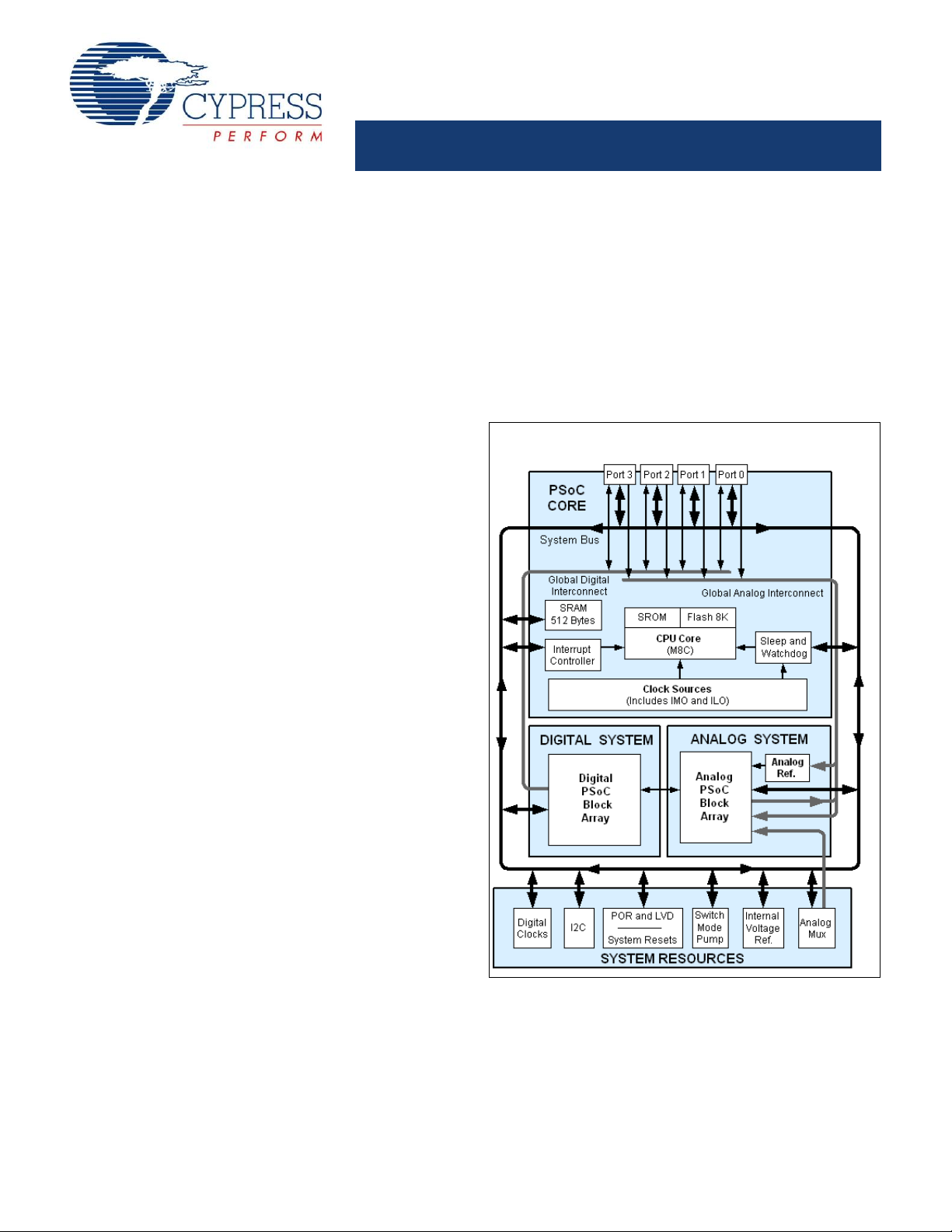
The PSoC family consists of many Mixed-Signal Array with
On-Chip Controller devices. These devices are designed to
replace multiple traditional MCU-based system components with
one low cost single-chip programmable component. A PSoC
device includes configurable blocks of analog and digital logic,
and programmable interconnect. This architecture enables the
user to create customized peripheral configurations, to match
the requirements of each individual application. Additionally, a
fast CPU, Flash program memory, SRAM data memory, and
configurable IO are included in a range of convenient pinouts.
The PSoC architecture, shown in Figure 1, consists of four main
areas: the Core, the System Resources, the Digital System, and
the Analog System. Configurable global bus resources allow
combining all the device resources into a complete custom
system. Each CY8C21x34 PSoC device includes four digital
blocks and four analog blocks. Depending on the PSoC
package, up to 28 general purpose IO (GPIO) are also included.
The GPIO provide access to the global digital and analog interconnects.
The PSoC Core
The PSoC Core is a powerful engine that supports a rich
instruction set. It encompasses SRAM for data storage, an
interrupt controller, sleep and watchdog timers, and IMO
(internal main oscillator) and ILO (internal low speed oscillator).
The CPU core, called the M8C, is a powerful processor with
speeds up to 24 MHz. The M8C is a four MIPS 8-bit Harvard
architecture microprocessor.
System Resources provide the following additional capabilities:
■ Digital clocks to increase the flexibility of the PSoC
mixed-signal arrays.
■ I2C functionality to implement an I2C master and slave.
■ An internal voltage reference, MultiMaster, that provides an
absolute value of 1.3V to a number of PSoC subsystems.
■ A switch mode pump (SMP) that generates normal operating
voltages off a single battery cell.
■ Various system resets supported by the M8C.
The Digital System consists of an array of digital PSoC blocks
that may be configured into any number of digital peripherals.
The digital blocks are connected to the GPIO through a series of
global buses that can route any signal to any pin, freeing designs
from the constraints of a fixed peripheral controller.
The Analog System consists of four analog PSoC blocks,
supporting comparators and analog-to-digital conversion up to 8
bits in precision.
The Digital System
The Digital System consists of 4 digital PSoC blocks. Each block
is an 8-bit resource that is used alone or combined with other
blocks to form 8, 16, 24, and 32-bit peripherals, which are called
user module references. Digital peripheral configurations include
the following.
■ PWMs (8 to 32 bit)
■ PWMs with Dead band (8 to 32 bit)
■ Counters (8 to 32 bit)
■ Timers (8 to 32 bit)
■ UART 8 bit with selectable parity
■ SPI master and slave
■ I2C slave and multi-master
■ Cyclical Redundancy Checker/Generator (8 to 32 bit)
■ IrDA
■ Pseudo Random Sequence Generators (8 to 32 bit)
The digital blocks are connected to any GPIO through a series
of global buses that can route any signal to any pin. The buses
also allow for signal multiplexing and for performing logic
operations. This configurability frees your designs from the
constraints of a fixed peripheral controller.
Digital blocks are provided in rows of four, where the number of
blocks varies by PSoC device family. This allows the optimum
choice of system resources for your application. Family
resources are shown in Ta b le 1 on page 4.
Figure 1. Digital System Block Diagram
Document Number: 38-12025 Rev. *O Page 2 of 45
[+] Feedback
Page 3
CY8C21634, CY8C21534
CY8C21434, CY8C21334, CY8C21234
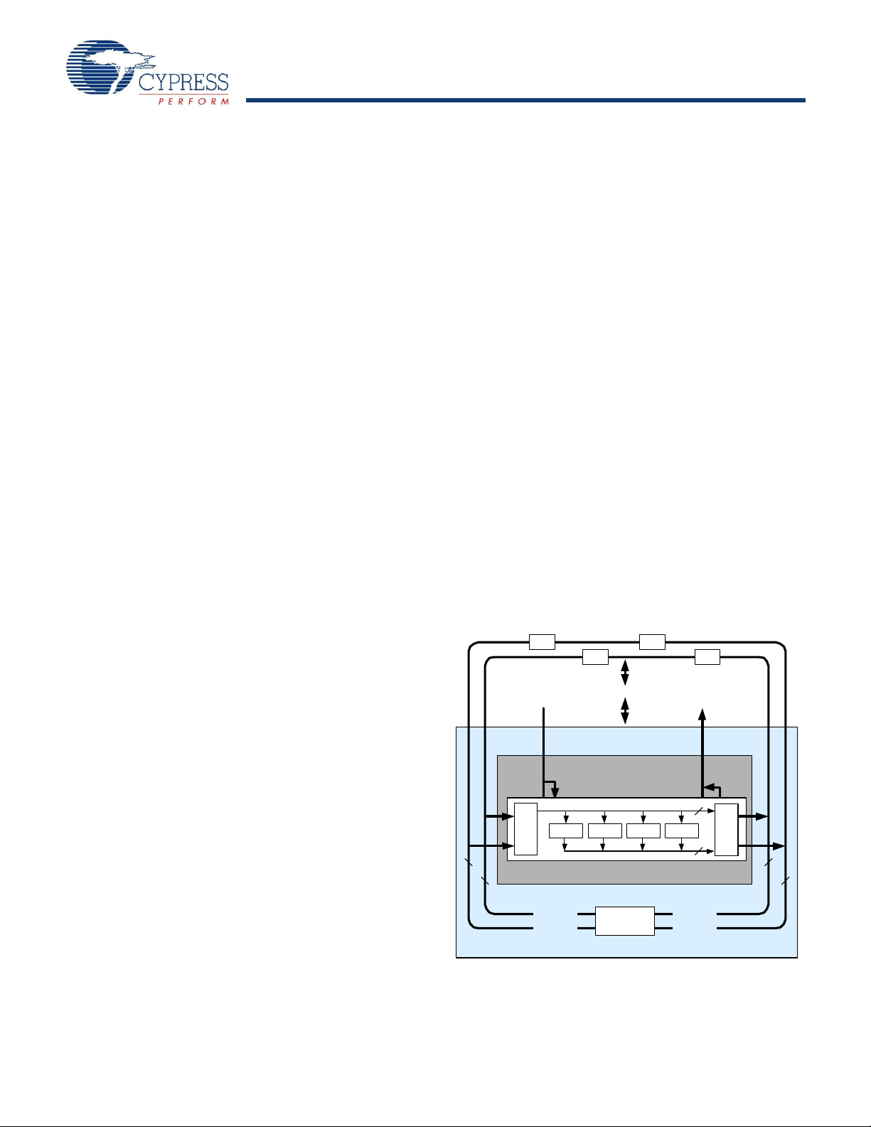
The Analog System
AC O L 1 M U X
ACE00 ACE01
Array
Array Input
Configuration
ASE10 ASE11
X
X
X
X
X
An a l o g Mux Bus
All IO
ACI0[1:0] ACI1[1:0]
The Analog System consists of 4 configurable blocks that allow
the creation of complex analog signal flows. Analog peripherals
are very flexible and may be customized to support specific
application requirements. Some of the common PSoC analog
functions for this device (most available as user modules) are:
■ Analog-to-digital converters (single or dual, with 8-bit or 10-bit
resolution)
■ Pin-to-pin comparator
■ Single-ended comparators (up to 2) with absolute (1.3V)
reference or 8-bit DAC reference
■ 1.3V reference (as a System Resource)
In most PSoC devices, analog blocks are provided in columns of
three, which includes one CT (Continuous Time) and two SC
(Switched Capacitor) blocks. The CY8C21x34 devices provide
limited functionality Type “E” analog blocks. Each column
contains one CT Type E block and one SC Type E block. Refer
to the PSoC Programmable System-on-Chip™ Technical
Reference Manual for detailed information on the CY8C21x34’s
Type E analog blocks.
Figure 2. Analog System Block Diagram
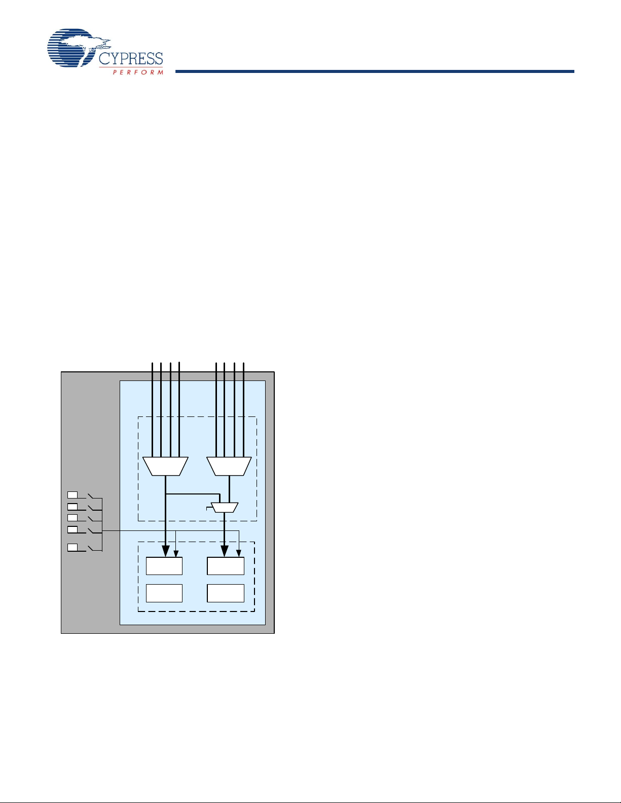
The Analog Multiplexer System
The Analog Mux Bus can connect to every GPIO pin. Pins may
be connected to the bus individually or in any combination. The
bus also connects to the analog system for analysis with
comparators and analog-to-digital converters. An additional 8:1
analog input multiplexer provides a second path to bring Port 0
pins to the analog array.
Switch control logic enables selected pins to precharge
continuously under hardware control. This enables capacitive
measurement for applications such as touch sensing. Other
multiplexer applications include:
■ Track pad, finger sensing.
■ Chip-wide mux that allows analog input from any IO pin.
■ Crosspoint connection between any IO pin combinations.
When designing capacitive sensing applications, refer to the
signal-to-noise system level requirement found in Application
Note AN2403 on the Cypress web site at
http://www.cypress.com.
Additional System Resources
System Resources, some of which are listed in the previous
sections, provide additional capability useful to complete
systems. Additional resources include a switch mode pump, low
voltage detection, and power on reset. Brief statements
describing the merits of each system resource follow.
■ Digital clock dividers provide three customizable clock
frequencies for use in applications. The clocks may be routed
to both the digital and analog systems. Additional clocks can
be generated using digital PSoC blocks as clock dividers.
■ The I2C module provides 100 and 400 kHz communication over
two wires. Slave, master, and multi-master modes are all
supported.
■ Low Voltage Detection (LVD) interrupts can signal the
application of falling voltage levels, while the advanced POR
(Power On Reset) circuit eliminates the need for a system
supervisor.
■ An internal 1.3 voltage reference provides an absolute
reference for the analog system, including ADCs and DACs.
■ An integrated switch mode pump (SMP) generates normal
operating voltages from a single 1.2V battery cell, providing a
low cost boost converter.
■ Versatile analog multiplexer system.
Document Number: 38-12025 Rev. *O Page 3 of 45
[+] Feedback
Page 4
CY8C21634, CY8C21534
CY8C21434, CY8C21334, CY8C21234
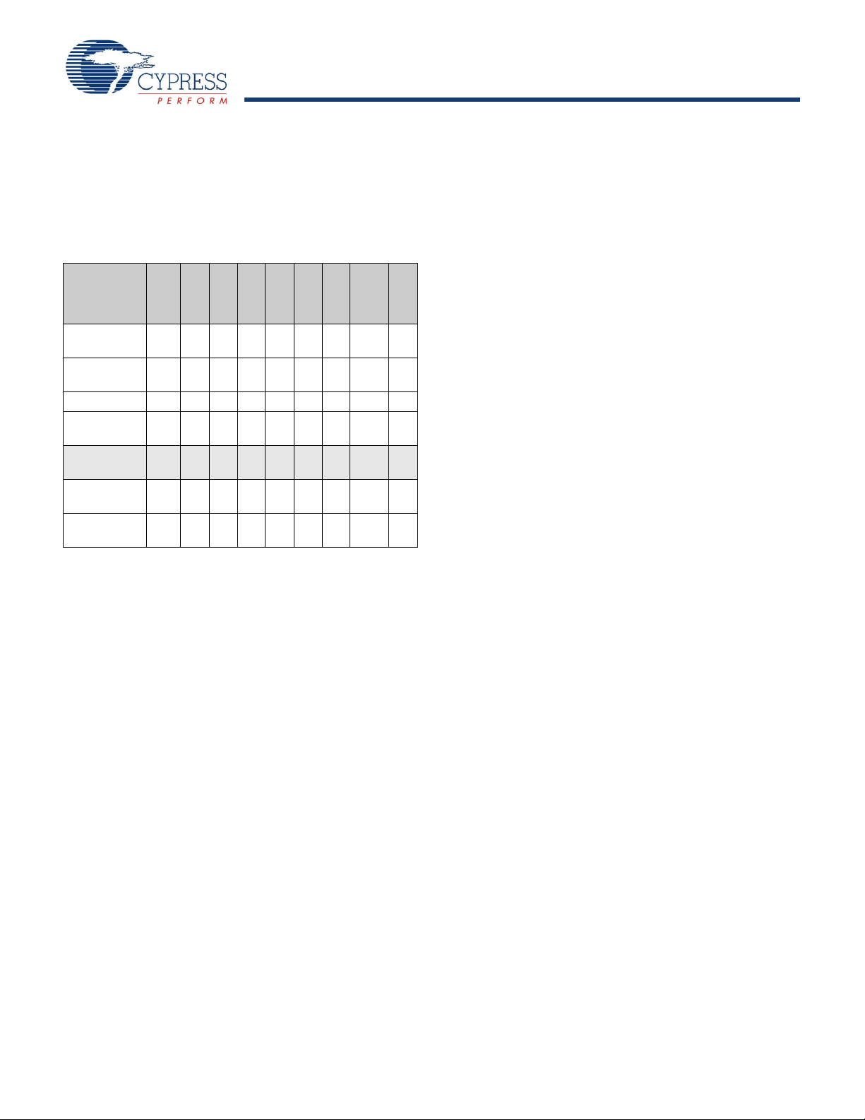
PSoC Device Characteristics
Notes
1. Limited analog functionality
.
2. Two analog blocks and one CapSense.
Depending on your PSoC device characteristics, the digital and
analog systems can have 16, 8, or 4 digital blocks and 12, 6, or
4 analog blocks. Table 1 lists the resources available for specific
PSoC device groups. The PSoC device covered by this data
sheet is highlighted in this table.
Table 1. PSoC Device Characteristics
PSoC Part
Number
CY8C29x66 up to 644 16 12 4 4 12 2K 32K
CY8C27x43
CY8C24x94 56 1 4 48 2 2 6 1K 16K
CY8C24x23A
CY8C21x34 up to 281 4 28 0 2 4
CY8C21x23
CY8C20x34
Digital IODigital
up to 442 8 12 4 4 12 256
up to 241 4 12 2 2 6 256
16 1 4 8 0 2 4
up to 280 0 28 0 0 3
Rows
Digital
Blocks
Analog
Inputs
Analog
Analog
Outputs
Analog
Columns
[1]
[1]
[2]
Blocks
Bytes
Bytes
512
Bytes
256
Bytes
512
Bytes
Size
SRAM
16K
4K
8K
4K
8K
Flash
Getting Started
The quickest way to understand PSoC silicon is to read this data
sheet and then use the PSoC Designer Integrated Development
Environment (IDE). This data sheet is an overview of the PSoC
integrated circuit and presents specific pin, register, and
electrical specifications.
For in depth information, along with detailed programming
details, see the PSoC® Programmable System-on-Chip
Technical Reference Manual for CY8C28xxx PSoC devices.
For up-to-date ordering, packaging, and electrical specification
information, see the latest PSoC device data sheets on the web
at www.cypress.com/psoc.
Application Notes
Application notes are an excellent introduction to the wide variety
of possible PSoC designs. They are located here:
www.cypress.com/psoc. Select Application Notes under the
Documentation tab.
Development Kits
Size
PSoC Development Kits are available online from Cypress at
www.cypress.com/shop and through a growing number of
regional and global distributors, which include Arrow, Avnet,
Digi-Key, Farnell, Future Electronics, and Newark.
Training
Free PSoC technical training (on demand, webinars, and
workshops) is available online at www.cypress.com/training. The
training covers a wide variety of topics and skill levels to assist
you in your designs.
Cypros Consultants
Certified PSoC Consultants offer everything from technical
assistance to completed PSoC designs. To contact or become a
PSoC Consultant go to www.cypress.com/cypros.
Solutions Library
Visit our growing library of solution focused designs at
www.cypress.com/solutions. Here you can find various application designs that include firmware and hardware design files
that enable you to complete your designs quickly.
Technical Support
For assistance with technical issues, search KnowledgeBase
articles and forums at www.cypress.com/support. If you cannot
find an answer to your question, call technical support at
1-800-541-4736.
Document Number: 38-12025 Rev. *O Page 4 of 45
[+] Feedback
Page 5

CY8C21634, CY8C21534
CY8C21434, CY8C21334, CY8C21234
Development Tools
PSoC Designer is a Microsoft® Windows-based, integrated
development environment for the Programmable
System-on-Chip (PSoC) devices. The PSoC Designer IDE runs
on Windows XP or Windows Vista.
This system provides design database management by project,
an integrated debugger with In-Circuit Emulator, in-system
programming support, and built-in support for third-party
assemblers and C compilers.
PSoC Designer also supports C language compilers developed
specifically for the devices in the PSoC family.
PSoC Designer Software Subsystems
System-Level View
A drag-and-drop visual embedded system design environment
based on PSoC Express. In the system level view you create a
model of your system inputs, outputs, and communication interfaces. You define when and how an output device changes state
based upon any or all other system devices. Based upon the
design, PSoC Designer automatically selects one or more PSoC
Mixed-Signal Controllers that match your system requirements.
PSoC Designer generates all embedded code, then compiles
and links it into a programming file for a specific PSoC device.
Chip-Level View
The chip-level view is a more traditional Integrated Development
Environment (IDE) based on PSoC Designer 4.4. Choose a base
device to work with and then select different onboard analog and
digital components called user modules that use the PSoC
blocks. Examples of user modules are ADCs, DACs, Amplifiers,
and Filters. Configure the user modules for your chosen
application and connect them to each other and to the proper
pins. Then generate your project. This prepopulates your project
with APIs and libraries that you can use to program your
application.
The device editor also supports easy development of multiple
configurations and dynamic reconfiguration. Dynamic
configuration allows for changing configurations at run time.
Hybrid Designs
You can begin in the system-level view, allow it to choose and
configure your user modules, routing, and generate code, then
switch to the chip-level view to gain complete control over
on-chip resources. All views of the project share a common code
editor, builder, and common debug, emulation, and programming
tools.
Code Generation Tools
PSoC Designer supports multiple third party C compilers and
assemblers. The code generation tools work seamlessly within
the PSoC Designer interface and have been tested with a full
range of debugging tools. The choice is yours.
Assemblers. The assemblers allow assembly code to merge
seamlessly with C code. Link libraries automatically use absolute
addressing or are compiled in relative mode, and linked with
other software modules to get absolute addressing.
C Language Compilers. C language compilers are available
that support the PSoC family of devices. The products allow you
to create complete C programs for the PSoC family devices.
The optimizing C compilers provide all the features of C tailored
to the PSoC architecture. They come complete with embedded
libraries providing port and bus operations, standard keypad and
display support, and extended math functionality.
Debugger
The PSoC Designer Debugger subsystem provides hardware
in-circuit emulation, allowing you to test the program in a physical
system while providing an internal view of the PSoC device.
Debugger commands allow the designer to read and program
and read and write data memory, read and write IO registers,
read and write CPU registers, set and clear breakpoints, and
provide program run, halt, and step control. The debugger also
allows the designer to create a trace buffer of registers and
memory locations of interest.
Online Help System
The online help system displays online, context-sensitive help
for the user. Designed for procedural and quick reference, each
functional subsystem has its own context-sensitive help. This
system also provides tutorials and links to FAQs and an Online
Support Forum to aid the designer in getting started.
In-Circuit Emulator
A low cost, high functionality In-Circuit Emulator (ICE) is
available for development support. This hardware has the
capability to program single devices.
The emulator consists of a base unit that connects to the PC by
way of a USB port. The base unit is universal and operates with
all PSoC devices. Emulation pods for each device family are
available separately. The emulation pod takes the place of the
PSoC device in the target board and performs full speed (24
MHz) operation.
Document Number: 38-12025 Rev. *O Page 5 of 45
[+] Feedback
Page 6

CY8C21634, CY8C21534
CY8C21434, CY8C21334, CY8C21234
Designing with PSoC Designer
The development process for the PSoC device differs from that
of a traditional fixed function microprocessor. The configurable
analog and digital hardware blocks give the PSoC architecture a
unique flexibility that pays dividends in managing specification
change during development and by lowering inventory costs.
These configurable resources, called PSoC Blocks, have the
ability to implement a wide variety of user-selectable functions.
The PSoC development process can be summarized in the
following four steps:
1. Select components
2. Configure components
3. Organize and Connect
4. Generate, Verify, and Debug
Select Components
Both the system-level and chip-level views provide a library of
prebuilt, pretested hardware peripheral components. In the
system-level view, these components are called “drivers” and
correspond to inputs (a thermistor, for example), outputs (a
brushless DC fan, for example), communication interfaces
2
(I
C-bus, for example), and the logic to control how they interact
with one another (called valuators).
In the chip-level view, the components are called “user modules”.
User modules make selecting and implementing peripheral
devices simple, and come in analog, digital, and mixed signal
varieties.
Configure Components
Each of the components you select establishes the basic register
settings that implement the selected function. They also provide
parameters and properties that allow you to tailor their precise
configuration to your particular application. For example, a Pulse
Width Modulator (PWM) User Module configures one or more
digital PSoC blocks, one for each 8 bits of resolution. The user
module parameters permit you to establish the pulse width and
duty cycle. Configure the parameters and properties to
correspond to your chosen application. Enter values directly or
by selecting values from drop-down menus.
Both the system-level drivers and chip-level user modules are
documented in data sheets that are viewed directly in the PSoC
Designer. These data sheets explain the internal operation of the
component and provide performance specifications. Each data
sheet describes the use of each user module parameter or driver
property, and other information you may need to successfully
implement your design.
Organize and Connect
You can build signal chains at the chip level by interconnecting
user modules to each other and the IO pins, or connect system
level inputs, outputs, and communication interfaces to each
other with valuator functions.
In the system-level view, selecting a potentiometer driver to
control a variable speed fan driver and setting up the valuators
to control the fan speed based on input from the pot selects,
places, routes, and configures a programmable gain amplifier
(PGA) to buffer the input from the potentiometer, an analog to
digital converter (ADC) to convert the potentiometer’s output to
a digital signal, and a PWM to control the fan.
In the chip-level view, perform the selection, configuration, and
routing so that you have complete control over the use of all
on-chip resources.
Generate, Verify, and Debug
When you are ready to test the hardware configuration or move
on to developing code for the project, perform the “Generate
Application” step. This causes PSoC Designer to generate
source code that automatically configures the device to your
specification and provides the software for the system.
Both system-level and chip-level designs generate software
based on your design. The chip-level design provides application
programming interfaces (APIs) with high level functions to
control and respond to hardware events at run-time and interrupt
service routines that you can adapt as needed. The system-level
design also generates a C main() program that completely
controls the chosen application and contains placeholders for
custom code at strategic positions allowing you to further refine
the software without disrupting the generated code.
A complete code development environment allows you to
develop and customize your applications in C, assembly
language, or both.
The last step in the development process takes place inside the
PSoC Designer’s Debugger subsystem. The Debugger
downloads the HEX image to the ICE where it runs at full speed.
Debugger capabilities rival those of systems costing many times
more. In addition to traditional single-step, run-to-breakpoint and
watch-variable features, the Debugger provides a large trace
buffer and allows you define complex breakpoint events that
include monitoring address and data bus values, memory
locations and external signals.
Document Number: 38-12025 Rev. *O Page 6 of 45
[+] Feedback
Page 7
CY8C21634, CY8C21534
CY8C21434, CY8C21334, CY8C21234
Document Conventions
Acronyms Used
The following table lists the acronyms that are used in this
document.
Table 2. Acronyms Used
Acronym Description
AC alternating current
ADC analog-to-digital converter
API application programming interface
CPU central processing unit
CT continuous time
DAC digital-to-analog converter
DC direct current
ECO external crystal oscillator
EEPROM electrically erasable programmable read-only
memory
FSR full scale range
GPIO general purpose IO
GUI graphical user interface
HBM human body model
ICE in-circuit emulator
ILO internal low speed oscillator
IMO internal main oscillator
IO input/output
IPOR imprecise power on reset
LSb least-significant bit
LVD low voltage detect
MSb most-significant bit
PC program counter
PLL phase-locked loop
POR power on reset
PPOR precision power on reset
PSoC® Programmable System-on-Chip™
PWM pulse width modulator
SC switched capacitor
SLIMO slow IMO
SMP switch mode pump
SRAM static random access memory
Units of Measure
A units of measure table is located in the Electrical Specifications
section. Table 2 on page 7 lists all the abbreviations used to
measure the PSoC devices.
Numeric Naming
Hexadecimal numbers are represented with all letters in
uppercase with an appended lowercase ‘h’ (for example, ‘14h’ or
‘3Ah’). Hexadecimal numbers may also be represented by a ‘0x’
prefix, the C coding convention. Binary numbers have an
appended lowercase ‘b’ (for example, 01010100b’ or
‘01000011b’). Numbers not indicated by an ‘h’, ‘b’, or 0x are
decimal.
Document Number: 38-12025 Rev. *O Page 7 of 45
[+] Feedback
Page 8
CY8C21634, CY8C21534
CY8C21434, CY8C21334, CY8C21234
Pin Information
Note
3. These are the ISSP pins, which are not High Z at POR (Power On Reset). See the PSoC Programmable System-on-Chip Technical Reference Manual for details.
SOIC
Vd d
P0[6 ], A, I, M
P0[4 ], A, I, M
P0[2 ], A, I, M
P0[0 ], A, I, M
P1[4 ], EXTCL K, M
P1[2 ], M
P1[0 ], I2 C SDA, M
16
15
14
13
12
11
1
2
3
4
5
6
7
8
A, I, M, P0[7]
A, I, M, P0[5]
A, I, M, P0[3]
A, I, M, P0[1]
SMP
Vss
M, I2C SCL , P1 [1 ]
Vss
10
9
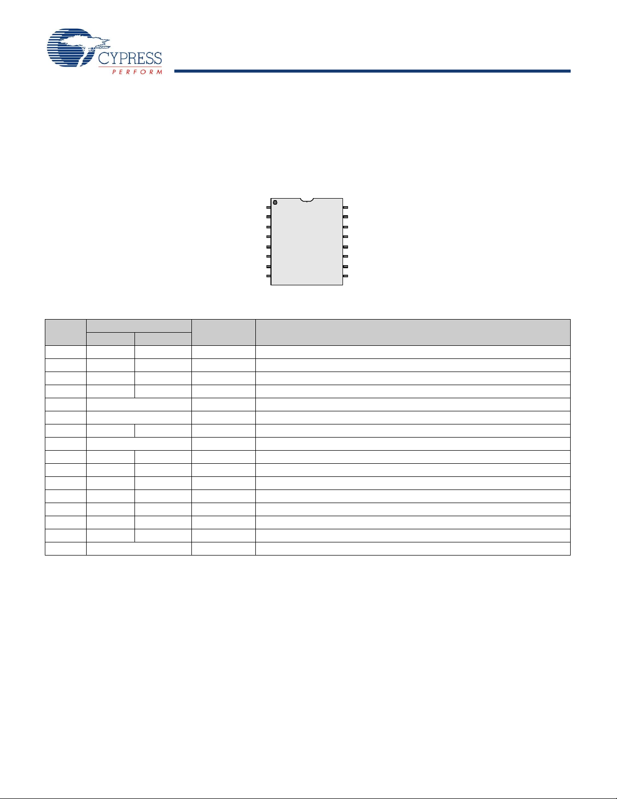
The CY8C21x34 PSoC device is available in a variety of packages which are listed in the following tables. Every port pin (labeled with
a “P”) is capable of Digital IO and connection to the common analog bus. However, Vss, Vdd, SMP, and XRES are not capable of
Digital IO.
16-Pin Part Pinout
Figure 3. CY8C21234 16-Pin PSoC Device
Table 3. Pin Definitions - CY8C21234 16-Pin (SOIC)
Pin No.
Digital Analog
1 IO I, M P0[7] Analog column mux input.
2 IO I, M P0[5] Analog column mux input.
3 IO I, M P0[3] Analog column mux input, integrating input.
4 IO I, M P0[1] Analog column mux input, integrating input.
5 Power SMP Switch Mode Pump (SMP) connection to required external components.
6 Power Vss Ground connection.
7 IO M P1[1] I2C Serial Clock (SCL), ISSP-SCLK
8 Power Vss Ground connection.
9 IO M P1[0] I2C Serial Data (SDA), ISSP-SDATA
10 IO M P1[2]
11 IO M P1[4] Optional External Clock Input (EXTCLK).
12 IO I, M P0[0] Analog column mux input.
13 IO I, M P0[2] Analog column mux input.
14 IO I, M P0[4] Analog column mux input.
15 IO I, M P0[6] Analog column mux input.
16 Power Vdd Supply voltage.
LEGEND A = Analog, I = Input, O = Output, and M = Analog Mux Input.
Type
Name Description
[3]
.
[3]
..
Document Number: 38-12025 Rev. *O Page 8 of 45
[+] Feedback
Page 9
CY8C21634, CY8C21534
CY8C21434, CY8C21334, CY8C21234
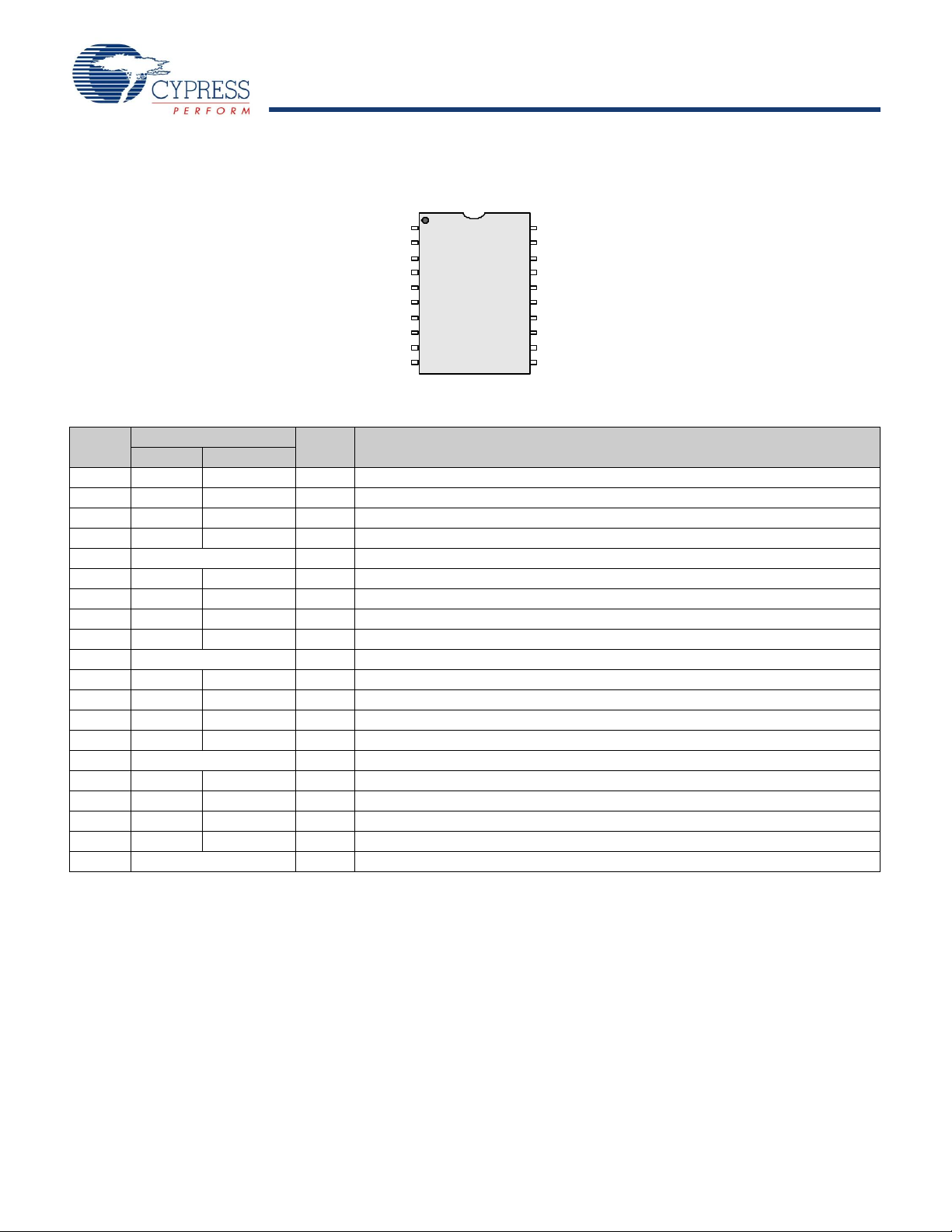
20-Pin Part Pinout
SSOP
Vd d
P0[6 ], A, I, M
P0[4 ], A, I, M
P0[2 ], A, I, M
P0[0 ], A, I, M
XRES
P1[6 ], M
P1[4 ], EXTCL K, M
P1[2 ], M
P1[0 ], I2 C SDA, M
20
19
18
17
16
15
14
13
12
11
1
2
3
4
5
6
7
8
9
10
A, I, M, P0[7]
A, I, M, P0[5]
A, I, M, P0[3]
A, I, M, P0[1]
M, I2C SC L , P1 [7 ]
SDA, P1 [ 5 ]
M, P1 [3 ]
SCL , P1[ 1 ]
Vss
Vss
M, I2 C
M, I2 C
Figure 4. CY8C21334 20-Pin PSoC Device
Table 4. Pin Definitions - CY8C21334 20-Pin (SSOP)
Pin No.
Digital Analog
1 IO I, M P0[7] Analog column mux input.
2 IO I, M P0[5] Analog column mux input.
3 IO I, M P0[3] Analog column mux input, integrating input.
4 IO I, M P0[1] Analog column mux input, integrating input.
5 Power Vss Ground connection.
6 IO M P1[7] I2C Serial Clock (SCL).
7 IO M P1[5] I2C Serial Data (SDA).
8 IO M P1[3]
9 IO M P1[1] I2C Serial Clock (SCL), ISSP-SCLK
10 Power Vss Ground connection.
11 IO M P1[0] I2C Serial Data (SDA), ISSP-SDATA
12 IO M P1[2]
13 IO M P1[4] Optional External Clock Input (EXTCLK).
14 IO M P1[6]
15 Input XRES Active high external reset with internal pull down.
16 IO I, M P0[0] Analog column mux input.
17 IO I, M P0[2] Analog column mux input.
18 IO I, M P0[4] Analog column mux input.
19 IO I, M P0[6] Analog column mux input.
20 Power Vdd Supply voltage.
LEGEND A = Analog, I = Input, O = Output, and M = Analog Mux Input.
Type
Name Description
[3]
.
[3]
.
Document Number: 38-12025 Rev. *O Page 9 of 45
[+] Feedback
Page 10
CY8C21634, CY8C21534
CY8C21434, CY8C21334, CY8C21234
28-Pin Part Pinout
A, I, M, P0[7]
A, I, M, P0[5]
A, I, M, P0[3]
A, I, M, P0[1]
M, P2 [7 ]
M, P2 [5 ]
M, P2 [3 ]
M, P2 [1 ]
Vss
M, I2 C SC L , P1 [ 7 ]
M, I2 C SDA, P1[ 5]
M, P1 [3 ]
M, I2 C SC L , P1 [ 1 ]
Vss
Vdd
P0[6], A, I, M
P0[4], A, I, M
P0[2], A, I, M
P0[0], A, I, M
P2[6 ], M
P2[4 ], M
P2[2 ], M
P2[0 ], M
XRES
P1[6 ], M
P1[4 ], EXTCL K, M
P1[2 ], M
P1[0], I2C SDA, M
SSOP
1
2
3
4
5
6
7
8
9
10
11
12
13
14
28
27
26
25
24
23
22
21
20
19
18
17
16
15
Figure 5. CY8C21534 28-Pin PSoC Device
Table 5. Pin Definitions - CY8C21534 28-Pin (SSOP)
Pin No.
Digital Analog
1 IO I, M P0[7] Analog column mux input.
2 IO I, M P0[5] Analog column mux input and column output.
3 IO I, M P0[3] Analog column mux input and column output, integrating input.
4 IO I, M P0[1] Analog column mux input, integrating input.
5 IO M P2[7]
6 IO M P2[5]
7 IO I, M P2[3] Direct switched capacitor block input.
8 IO I, M P2[1] Direct switched capacitor block input.
9 Power Vss Ground connection.
10 IO M P1[7] I2C Serial Clock (SCL).
11 IO M P1[5] I2C Serial Data (SDA).
12 IO M P1[3]
13 IO M P1[1] I2C Serial Clock (SCL), ISSP-SCLK
14 Power Vss Ground connection.
15 IO M P1[0] I2C Serial Data (SDA), ISSP-SDATA
16 IO M P1[2]
17 IO M P1[4] Optional External Clock Input (EXTCLK).
18 IO M P1[6]
19 Input XRES Active high external reset with internal pull down.
20 IO I, M P2[0] Direct switched capacitor block input.
21 IO I, M P2[2] Direct switched capacitor block input.
22 IO M P2[4]
23 IO M P2[6]
24 IO I, M P0[0] Analog column mux input.
25 IO I, M P0[2] Analog column mux input.
26 IO I, M P0[4] Analog column mux input
27 IO I, M P0[6] Analog column mux input.
28 Power Vdd Supply voltage.
LEGEND A: Analog, I: Input, O = Output, and M = Analog Mux Input.
Document Number: 38-12025 Rev. *O Page 10 of 45
Typ e
Name Description
[3]
.
[3]
.
[+] Feedback
Page 11
CY8C21634, CY8C21534
CY8C21434, CY8C21334, CY8C21234
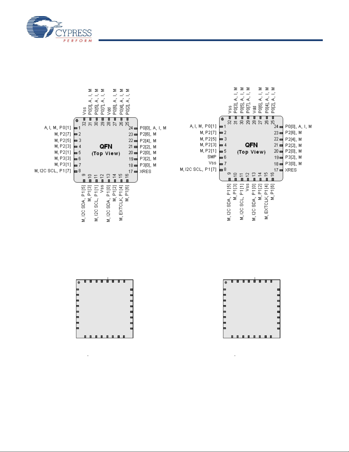
32-Pin Part Pinout
A, I, M, P0[1]
M, P2[7]
M, P2[5]
M, P2[3]
M, P2[1]
SMP
QFN
(Top View)
9
101112
131415
16
1
2
3
4
5
6
7
8
24
23
22
21
20
19
18
17
32313029282726
25
Vss
P0[3], A, I, M
P0[7], A, I, M
Vdd
P0[6], A, I, M
P0[4], A, I, M
P0[2], A, I, M
Vss
M, 12C SCL, P1[7]
P0[0], A, I, M
P2[6], M
P3[0], M
XRES
M, 12C SDA, P1[5]
M, P1[3]
M, 12C SCL, P1[1]
Vss
M, 12C SDA, P1[0]
M, P1[2]
M, EXTCLK, P1[4]
M, P1[6]
P2[4], M
P2[2], M
P2[0], M
P3[2], M
P0[5], A, I, M
Figure 6. CY8C21434 32-Pin PSoC Device
Figure 9. CY8C21634 32-Pin PSoC Device
A, I, M, P0[1]
M, P2[7]
M, P2[5]
M, P2[3]
M, P2[1]
M, P3[3]
QFN
(Top View)
9
101112
131415
16
1
2
3
4
5
6
7
8
24
23
22
21
20
19
18
17
32313029282726
25
Vss
P0[3], A, I, M
P0[7], A, I, M
Vdd
P0[6], A, I, M
P0[4], A, I, M
P0[2], A, I, M
M, P3[1]
M, 12C SCL, P1[7]
P0[0], A, I, M
P2[6], M
P3[0], M
XRES
M, 12C SDA, P1[5]
M, P1[3]
M, 12C SCL, P1[1]
Vss
M, 12C SDA, P1[0]
M, P1[2]
M, EXTCLK, P1[4]
M, P1[6]
P2[4], M
P2[2], M
P2[0], M
P3[2], M
P0[5], A, I, M
Figure 10. CY8C21434 32-Pin Sawn PSoC Device Figure 11. CY8C21634 32-Pin Sawn PSoC Device
Document Number: 38-12025 Rev. *O Page 11 of 45
[+] Feedback
Page 12
CY8C21634, CY8C21534
CY8C21434, CY8C21334, CY8C21234
Table 6. Pin Definitions - CY8C21434/CY8C21634 32-Pin (QFN)
Note
4. The center pad on the QFN package must be connected to ground (Vss) for best mechanical, thermal, and electrical performance. If not connected to ground, it
must be electrically floated and not connected to any other signal.
Pin
No.
Digital Analog
Typ e
Name Description
[4]
1 IO I, M P0[1] Analog column mux input, integrating input.
2 IO M P2[7]
3 IO M P2[5]
4 IO M P2[3]
5 IO M P2[1]
6 IO M P3[3] In CY8C21434 part.
6 Power SMP Switch Mode Pump (SMP) connection to required external components in
CY8C21634 part.
7 IO M P3[1] In CY8C21434 part.
7 Power Vss Ground connection in CY8C21634 part.
8 IO M P1[7] I2C Serial Clock (SCL).
9 IO M P1[5] I2C Serial Data (SDA).
10 IO M P1[3]
11 IO M P1[1] I2C Serial Clock (SCL), ISSP-SCLK
[3]
.
12 Power Vss Ground connection.
13 IO M P1[0] I2C Serial Data (SDA), ISSP-SDATA
[3]
14 IO M P1[2]
15 IO M P1[4] Optional External Clock Input (EXTCLK).
16 IO M P1[6]
17 Input XRES Active high external reset with internal pull down.
18 IO M P3[0]
19 IO M P3[2]
20 IO M P2[0]
21 IO M P2[2]
22 IO M P2[4]
23 IO M P2[6]
24 IO I, M P0[0] Analog column mux input.
25 IO I, M P0[2] Analog column mux input.
26 IO I, M P0[4] Analog column mux input.
27 IO I, M P0[6] Analog column mux input.
28 Power Vdd Supply voltage.
29 IO I, M P0[7] Analog column mux input.
30 IO I, M P0[5] Analog column mux input.
31 IO I, M P0[3] Analog column mux input, integrating input.
32 Power Vss Ground connection.
A = Analog, I = Input, O = Output, and M = Analog Mux Input.
LEGEND
Document Number: 38-12025 Rev. *O Page 12 of 45
[+] Feedback
Page 13
CY8C21634, CY8C21534
CY8C21434, CY8C21334, CY8C21234
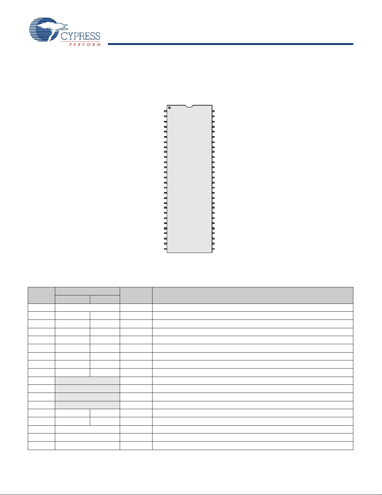
56-Pin Part Pinout
SSOP
1
56 Vdd
2
AI, P0[7]
55
P0[6], AI
3
AI, P0[5]
54
P0[4], AI
4
AI, P0[3]
53
P0[2], AI
5
AI, P0[1]
52
P0[0], AI
6
P2[7]
51
P2[6]
7
P2[5]
50
P2[4]
8
P2[3]
49
P2[2]
9P2[1] 48
P2[0]
10
NC
47
NC
11
NC
46
NC
12NC 45 P3[2]
13
NC
44
P3[0]
14OCDE 43
CCLK
15
OCDO
42
HCLK
16
SMP
41
XRES
17
Vss
40
NC
18
Vss
39
NC
19
P3[3]
38
NC
20
P3[1]
37
NC
21
NC
36
NC
22
NC
35
NC
23I2C SCL, P1[7] 34
P1[6]
24
I2C SDA, P1[5]
33
P1[4], EXTCLK
25
NC
32
P1[2]
26
P1[3]
31
P1[0], I2C
SDA, SDATA
27
SCLK, I2C SCL, P1[1]
30 NC
28Vss
29
NC
Vss
The 56-pin SSOP part is for the CY8C21001 On-Chip Debug (OCD) PSoC device.
Note This part is only used for in-circuit debugging. It is NOT available for production.
Figure 12. CY8C21001 56-Pin PSoC Device
Table 7. Pin Definitions - CY8C21001 56-Pin (SSOP)
Pin No.
Type
Digital Analog
Pin Name Description
1 Power Vss Ground connection.
2 IO I P0[7] Analog column mux input.
3 IO I P0[5] Analog column mux input and column output.
4 IO I P0[3] Analog column mux input and column output.
5 IO I P0[1] Analog column mux input.
6 IO P2[7]
7 IO P2[5]
8 IO I P2[3] Direct switched capacitor block input.
9 IO I P2[1] Direct switched capacitor block input.
10 NC No connection.
11 NC No connection.
12 NC No connection.
13 NC No connection.
14 OCD OCDE OCD even data IO.
15 OCD OCDO OCD odd data output.
16 Power SMP Switch Mode Pump (SMP) connection to required external components.
17 Power Vss Ground connection.
18 Power Vss Ground connection.
Document Number: 38-12025 Rev. *O Page 13 of 45
[+] Feedback
Page 14
CY8C21634, CY8C21534
CY8C21434, CY8C21334, CY8C21234
Table 7. Pin Definitions - CY8C21001 56-Pin (SSOP) (continued)
Pin No.
Type
Digital Analog
Pin Name Description
19 IO P3[3]
20 IO P3[1]
21 NC No connection.
22 NC No connection.
23 IO P1[7] I2C Serial Clock (SCL).
24 IO P1[5] I2C Serial Data (SDA).
25 NC No connection.
26 IO P1[3] I
27 IO P1[1] Crystal Input (XTALin), I2C Serial Clock (SCL), ISSP-SCLK
FMTEST
.
[3]
28 Power Vss Ground connection.
29 NC No connection.
30 NC No connection.
31 IO P1[0] Crystal Output (XTALout), I2C Serial Data (SDA), ISSP-SDATA
32 IO P1[2] V
FMTEST
.
33 IO P1[4] Optional External Clock Input (EXTCLK).
34 IO P1[6]
35 NC No connection.
36 NC No connection.
37 NC No connection.
38 NC No connection.
39 NC No connection.
40 NC No connection.
41 Input XRES Active high external reset with internal pull down.
42 OCD HCLK OCD high-speed clock output.
43 OCD CCLK OCD CPU clock output.
44 IO P3[0]
45 IO P3[2]
46 NC No connection.
47 NC No connection.
48 IO I P2[0]
49 IO I P2[2]
50 IO P2[4]
51 IO P2[6]
52 IO I P0[0] Analog column mux input.
53 IO I P0[2] Analog column mux input and column output.
54 IO I P0[4] Analog column mux input and column output.
55 IO I P0[6] Analog column mux input.
56 Power Vdd Supply voltage.
..
[3]
..
LEGEND: A = Analog, I = Input, O = Output, and OCD = On-Chip Debug.
Document Number: 38-12025 Rev. *O Page 14 of 45
[+] Feedback
Page 15
CY8C21634, CY8C21534
CY8C21434, CY8C21334, CY8C21234
Register Reference
This chapter lists the registers of the CY8C21x34 PSoC device. For detailed register information, refer the PSoC Programmable
System-on-Chip Technical Reference Manual.
Register Conventions
The register conventions specific to this section are listed in Ta b le 8 .
Table 8. Register Conventions
Convention Description
R Read register or bit(s)
W Write register or bit(s)
L Logical register or bit(s)
C Clearable register or bit(s)
# Access is bit specific
Register Mapping Tables
The PSoC device has a total register address space of 512 bytes. The register space is referred to as IO space and is divided into
two banks. The XOI bit in the Flag register (CPU_F) determines which bank the user is currently in. When the XOI bit is set the user
is in Bank 1.
Note In the following register mapping tables, blank fields are Reserved and must not be accessed.
Table 9. Register Map 0 Table: User Space
Name
PRT0DR 00 RW 40 ASE10CR0 80 RW C0
PRT0IE 01 RW 41 81 C1
PRT0GS 02 RW 42 82 C2
PRT0DM2 03 RW 43 83 C3
PRT1DR 04 RW 44 ASE11CR0 84 RW C4
PRT1IE 05 RW 45 85 C5
PRT1GS 06 RW 46 86 C6
PRT1DM2 07 RW 47 87 C7
PRT2DR 08 RW 48 88 C8
PRT2IE 09 RW 49 89 C9
PRT2GS 0A RW 4A 8A CA
PRT2DM2 0B RW 4B 8B CB
PRT3DR 0C RW 4C 8C CC
PRT3IE 0D RW 4D 8D CD
PRT3GS 0E RW 4E 8E CE
PRT3DM2 0F RW 4F 8F CF
Blank fields are Reserved and must not be accessed. # Access is bit specific.
Addr
(0,Hex)
10 50 90 CUR_PP D0 RW
11 51 91 STK_PP D1 RW
12 52 92 D2
13 53 93 IDX_PP D3 RW
14 54 94 MVR_PP D4 RW
15 55 95 MVW_PP D5 RW
16 56 96 I2C_CFG D6 RW
17 57 97 I2C_SCR D7 #
18 58 98 I2C_DR D8 RW
19 59 99 I2C_MSCR D9 #
1A 5A 9A INT_CLR0 DA RW
1B 5B 9B INT_CLR1 DB RW
1C 5C 9C DC
1D 5D 9D INT_CLR3 DD RW
1E 5E 9E INT_MSK3 DE RW
1F 5F 9F DF
Access
Name
Addr
(0,Hex)
Access
Name
Addr
(0,Hex)
Access
Name
Addr
(0,Hex)
Access
Document Number: 38-12025 Rev. *O Page 15 of 45
[+] Feedback
Page 16

CY8C21634, CY8C21534
CY8C21434, CY8C21334, CY8C21234
Table 9. Register Map 0 Table: User Space (continued)
Name
DBB00DR0 20 # AMX_IN 60 RW A0 INT_MSK0 E0 RW
DBB00DR1 21 W AMUXCFG 61 RW A1 INT_MSK1 E1 RW
DBB00DR2 22 RW PWM_CR 62 RW A2 INT_VC E2 RC
DBB00CR0 23 # 63 A3 RES_WDT E3 W
DBB01DR0 24 # CMP_CR0 64 # A4 E4
DBB01DR1 25 W 65 A5 E5
DBB01DR2 26 RW CMP_CR1 66 RW A6 DEC_CR0 E6 RW
DBB01CR0 27 # 67 A7 DEC_CR1 E7 RW
DCB02DR0 28 # ADC0_CR 68 # A8 E8
DCB02DR1 29 W ADC1_CR 69 # A9 E9
DCB02DR2 2A RW 6A AA EA
DCB02CR0 2B # 6B AB EB
DCB03DR0 2C # TMP_DR0 6C RW AC EC
DCB03DR1 2D W TMP_DR1 6D RW AD ED
DCB03DR2 2E RW TMP_DR2 6E RW AE EE
DCB03CR0 2F # TMP_DR3 6F RW AF EF
Blank fields are Reserved and must not be accessed. # Access is bit specific.
Addr
(0,Hex)
30 70 RDI0RI B0 RW F0
31 71 RDI0SYN B1 RW F1
32 ACE00CR1 72 RW RDI0IS B2 RW F2
33 ACE00CR2 73 RW RDI0LT0 B3 RW F3
34 74 RDI0LT1 B4 RW F4
35 75 RDI0RO0 B5 RW F5
36 ACE01CR1 76 RW RDI0RO1 B6 RW F6
37 ACE01CR2 77 RW B7 CPU_F F7 RL
38 78 B8 F8
39 79 B9 F9
3A 7A BA FA
3B 7B BB FB
3C 7C BC FC
3D 7D BD DAC_D FD RW
3E 7E BE CPU_SCR1 FE #
3F 7F BF CPU_SCR0 FF #
Access
Name
Addr
(0,Hex)
Access
Name
Addr
(0,Hex)
Access
Name
Addr
(0,Hex)
Access
Table 10. Register Map 1 Table: Configuration Space
Name
PRT0DM0 00 RW 40 ASE10CR0 80 RW C0
PRT0DM1 01 RW 41 81 C1
PRT0IC0 02 RW 42 82 C2
PRT0IC1 03 RW 43 83 C3
PRT1DM0 04 RW 44 ASE11CR0 84 RW C4
PRT1DM1 05 RW 45 85 C5
PRT1IC0 06 RW 46 86 C6
PRT1IC1 07 RW 47 87 C7
PRT2DM0 08 RW 48 88 C8
PRT2DM1 09 RW 49 89 C9
PRT2IC0 0A RW 4A 8A CA
PRT2IC1 0B RW 4B 8B CB
PRT3DM0 0C RW 4C 8C CC
PRT3DM1 0D RW 4D 8D CD
PRT3IC0 0E RW 4E 8E CE
PRT3IC1 0F RW 4F 8F CF
Blank fields are Reserved and must not be accessed. # Access is bit specific.
Addr
(1,Hex)
10 50 90 GDI_O_IN D0 RW
11 51 91 GDI_E_IN D1 RW
12 52 92 GDI_O_OU D2 RW
13 53 93 GDI_E_OU D3 RW
14 54 94 D4
Access
Name
Document Number: 38-12025 Rev. *O Page 16 of 45
Addr
(1,Hex)
Access
Name
Addr
(1,Hex)
Access
Name
Addr
(1,Hex)
Access
[+] Feedback
Page 17

CY8C21634, CY8C21534
CY8C21434, CY8C21334, CY8C21234
Table 10. Register Map 1 Table: Configuration Space (continued)
Name
DBB00FN 20 RW CLK_CR0 60 RW A0 OSC_CR0 E0 RW
DBB00IN 21 RW CLK_CR1 61 RW A1 OSC_CR1 E1 RW
DBB00OU 22 RW ABF_CR0 62 RW A2 OSC_CR2 E2 RW
DBB01FN 24 RW CMP_GO_EN 64 RW A4 VLT_CMP E4 R
DBB01IN 25 RW 65 A5 ADC0_TR E5 RW
DBB01OU 26 RW AMD_CR1 66 RW A6 ADC1_TR E6 RW
DCB02FN 28 RW 68 A8 IMO_TR E8 W
DCB02IN 29 RW 69 A9 ILO_TR E9 W
DCB02OU 2A RW 6A AA BDG_TR EA RW
DCB03FN 2C RW TMP_DR0 6C RW AC EC
DCB03IN 2D RW TMP_DR1 6D RW AD ED
DCB03OU 2E RW TMP_DR2 6E RW AE EE
Blank fields are Reserved and must not be accessed. # Access is bit specific.
Addr
(1,Hex)
15 55 95 D5
16 56 96 D6
17 57 97 D7
18 58 98 MUX_CR0 D8 RW
19 59 99 MUX_CR1 D9 RW
1A 5A 9A MUX_CR2 DA RW
1B 5B 9B MUX_CR3 DB RW
1C 5C 9C DC
1D 5D 9D OSC_GO_EN DD RW
1E 5E 9E OSC_CR4 DE RW
1F 5F 9F OSC_CR3 DF RW
23 AMD_CR0 63 RW A3 VLT_CR E3 RW
27 ALT_CR0 67 RW A7 E7
2B CLK_CR3 6B RW AB ECO_TR EB W
2F TMP_DR3 6F RW AF EF
30 70 RDI0RI B0 RW F0
31 71 RDI0SYN B1 RW F1
32 ACE00CR1 72 RW RDI0IS B2 RW F2
33 ACE00CR2 73 RW RDI0LT0 B3 RW F3
34 74 RDI0LT1 B4 RW F4
35 75 RDI0RO0 B5 RW F5
36 ACE01CR1 76 RW RDI0RO1 B6 RW F6
37 ACE01CR2 77 RW B7 CPU_F F7 RL
38 78 B8 F8
39 79 B9 F9
3A 7A BA FLS_PR1 FA RW
3B 7B BB FB
3C 7C BC FC
3D 7D BD DAC_CR FD RW
3E 7E BE CPU_SCR1 FE #
3F 7F BF CPU_SCR0 FF #
Access
Name
Addr
(1,Hex)
Access
Name
Addr
(1,Hex)
Access
Name
Addr
(1,Hex)
Access
Document Number: 38-12025 Rev. *O Page 17 of 45
[+] Feedback
Page 18

CY8C21634, CY8C21534
CY8C21434, CY8C21334, CY8C21234
Electrical Specifications
5.25
4.75
3.00
93 kHz 12 MHz 24 MHz
CPU Frequency
Vdd Voltage
5.25
4.75
3.00
93 kHz 12 MHz 24 MHz
IMO Frequency
Vdd Voltage
3.60
6 MHz
SLIMO Mode = 0
SLIMO
Mode=0
2.40
SLIMO
Mode=1
SLIMO
Mode=1
SLIMO
Mode=1
2.40
3 MHz
V
a
l
i
d
O
p
e
r
a
t
i
n
g
R
e
g
i
o
n
SLIMO
Mode=1
SLIMO
Mode=0
Figure 13. Voltage versus CPU Frequency Figure 14. IMO Frequency Trim Options
This section presents the DC and AC electrical specifications of the CY8C21x34 PSoC device. For up to date electrical specifications,
visit the web site http://www.cypress.com/psoc.
o
Specifications are valid for -40
Refer Table 25 on page 26 for the electrical specifications on the internal main oscillator (IMO) using SLIMO mode.
C ≤ TA ≤ 85oC and TJ ≤ 100oC as specified, except where noted.
Ta bl e 11 lists the units of measure that are used in this section.
Table 11. Units of Measure
Symbol Unit of Measure Symbol Unit of Measure
o
C degree Celsius μW microwatts
dB decibels mA milli-ampere
fF femto farad ms milli-second
Hz hertz mV milli-volts
KB 1024 bytes nA nanoampere
Kbit 1024 bits ns nanosecond
kHz kilohertz nV nanovolts
kΩ kilohm W ohm
MHz megahertz pA picoampere
MΩ megaohm pF picofarad
μA microampere pp peak-to-peak
μF microfarad ppm parts per million
μH microhenry ps picosecond
μs microsecond sps samples per second
μV microvolts s sigma: one standard deviation
μVrms microvolts root-mean-square V volts
Document Number: 38-12025 Rev. *O Page 18 of 45
[+] Feedback
Page 19

CY8C21634, CY8C21534
CY8C21434, CY8C21334, CY8C21234
Absolute Maximum Ratings
Table 12. Absolute Maximum Ratings
Symbol Description Min Typ Max Units Notes
T
STG
Storage Temperature -55 25 +100
o
C Higher storage temperatures
reduce data retention time. Recommended storage temperature is
o
+25
C ± 25oC. Extended duration
storage temperatures above 65
degrade reliability.
T
A
Ambient Temperature with Power Applied -40 – +85
o
C
Vdd Supply Voltage on Vdd Relative to Vss -0.5 – +6.0 V
V
V
I
MIO
IO
IOZ
DC Input Voltage Vss -
0.5
DC Voltage Applied to Tri-state Vss -
0.5
– Vdd +
0.5
– Vdd +
0.5
V
V
Maximum Current into any Port Pin -25 – +50 mA
ESD Electro Static Discharge Voltage 2000 – – V Human Body Model ESD.
LU Latch-up Current – – 200 mA
Operating Temperature
Table 13. Operating Temperature
Symbol Description Min Ty p Max Units Notes
T
A
T
J
Ambient Temperature -40 – +85
Junction Temperature -40 – +100
o
C
o
C The temperature rise from ambient
to junction is package specific. See
Table 40 on page 38. The user must
limit the power consumption to
comply with this requirement.
o
C
DC Electrical Characteristics
DC Chip-Level Specifications
Ta bl e 14 lists the guaranteed maximum and minimum specifications for the voltage and temperature ranges: 4.75V to 5.25V and -40°C
≤ 85°C, 3.0V to 3.6V and -40°C ≤ TA ≤ 85°C, or 2.4V to 3.0V and -40°C ≤ TA ≤ 85°C, respectively. Typical parameters apply to
≤ T
A
5V, 3.3V, or 2.7V at 25°C and are for design guidance only.
Table 14. DC Chip-Level Specifications
Symbol Description Min Typ Max Units Notes
Vdd Supply Voltage 2.40 – 5.25 V See Table 23 on page 24.
I
DD
I
DD3
I
DD27
Document Number: 38-12025 Rev. *O Page 19 of 45
Supply Current, IMO = 24 MHz – 3 4 mA Conditions are Vdd = 5.0V,
= 25oC, CPU = 3 MHz, 48 MHz
T
A
disabled. VC1 = 1.5 MHz,
VC2 = 93.75 kHz, VC3 = 0.366 kHz.
Supply Current, IMO = 6 MHz using SLIMO
mode.
– 1.2 2 mA Conditions are Vdd = 3.3V,
T
= 25oC, CPU = 3 MHz, clock
A
doubler disabled. VC1 = 375 kHz,
VC2 = 23.4 kHz, VC3 = 0.091 kHz.
Supply Current, IMO = 6 MHz using SLIMO
mode.
– 1.1 1.5 mA Conditions are Vdd = 2.55V,
= 25oC, CPU = 3 MHz, clock
T
A
doubler disabled. VC1 = 375 kHz,
VC2 = 23.4 kHz, VC3 = 0.091 kHz.
[+] Feedback
Page 20

CY8C21634, CY8C21534
CY8C21434, CY8C21334, CY8C21234
Table 14. DC Chip-Level Specifications (continued)
Symbol Description Min Typ Max Units Notes
I
SB27
Sleep (Mode) Current with POR, LVD, Sleep
Timer, WDT, and internal slow oscillator active.
– 2.6 4. μA Vdd = 2.55V, 0oC ≤ TA ≤ 40oC.
Mid temperature range.
I
SB
V
REF
V
REF27
AGND Analog Ground V
Sleep (Mode) Current with POR, LVD, Sleep
– 2.8 5 μA Vdd = 3.3V, -40oC ≤ TA ≤ 85oC.
Timer, WDT, and internal slow oscillator active.
Reference Voltage (Bandgap) 1.28 1.30 1.32 V Trimmed for appropriate Vdd.
Vdd = 3.0V to 5.25V.
Reference Voltage (Bandgap) 1.16 1.30 1.33 V Trimmed for appropriate Vdd. Vdd =
2.4V to 3.0V.
REF
- 0.003
V
REF
V
REF
+ 0.003
V
DC General Purpose IO Specifications
The following tables list the guaranteed maximum and minimum specifications for the voltage and temperature ranges: 4.75V to 5.25V
and -40°C ≤ T
apply to 5V, 3.3V, and 2.7V at 25°C and are for design guidance only.
≤ 85°C, 3.0V to 3.6V and -40°C ≤ TA ≤ 85°C, or 2.4V to 3.0V and -40°C ≤ TA ≤ 85°C, respectively. Typical parameters
A
Table 15. 5V and 3.3V DC GPIO Specifications
Symbol Description Min Typ Max Units Notes
R
PU
R
PD
V
OH
Pull up Resistor 4 5.6 8 kΩ
Pull down Resistor 4 5.6 8 kΩ
High Output Level Vdd -
– – V IOH = 10 mA, Vdd = 4.75 to 5.25V (8
1.0
total loads, 4 on even port pins (for
example, P0[2], P1[4]), 4 on odd port
pins (for example, P0[3], P1[5])).
V
OL
Low Output Level – – 0.75 V IOL = 25 mA, Vdd = 4.75 to 5.25V (8
total loads, 4 on even port pins (for
example, P0[2], P1[4]), 4 on odd port
pins (for example, P0[3], P1[5])).
V
V
V
I
C
C
IL
IH
H
IL
IN
OUT
Input Low Level – – 0.8 V Vdd = 3.0 to 5.25.
Input High Level 2.1 – V Vdd = 3.0 to 5.25.
Input Hysteresis – 60 – mV
Input Leakage (Absolute Value) – 1 – nA Gross tested to 1 μA.
Capacitive Load on Pins as Input – 3.5 10 pF Package and pin dependent.
Tem p = 2 5
Capacitive Load on Pins as Output – 3.5 10 pF Package and pin dependent.
Tem p = 2 5
o
C.
o
C.
Table 16. 2.7V DC GPIO Specifications
Symbol Description Min Typ Max Units Notes
R
PU
R
PD
V
OH
Pull up Resistor 4 5.6 8 kΩ
Pull down Resistor 4 5.6 8 kΩ
High Output Level Vdd -
– – V IOH = 2.5 mA (6.25 Typ), Vdd = 2.4
0.4
to 3.0V (16 mA maximum, 50 mA Typ
combined IOH budget).
V
OL
Low Output Level – – 0.75 V IOL = 10 mA, Vdd = 2.4 to 3.0V (90
mA maximum combined IOL
budget).
V
IL
Document Number: 38-12025 Rev. *O Page 20 of 45
Input Low Level – – 0.75 V Vdd = 2.4 to 3.0.
[+] Feedback
Page 21

CY8C21634, CY8C21534
CY8C21434, CY8C21334, CY8C21234
Table 16. 2.7V DC GPIO Specifications (continued)
Note
5. Atypical behavior: I
EBOA
of Port 0 Pin 0 is below 1 nA at 25°C; 50 nA over temperature. Use Port 0 Pins 1-7 for the lowest leakage of 200 nA.
Symbol Description Min Typ Max Units Notes
V
V
I
C
C
IH
H
IL
IN
OUT
Input High Level 2.0 – – V Vdd = 2.4 to 3.0.
Input Hysteresis – 90 – mV
Input Leakage (Absolute Value) – 1 – nA Gross tested to 1 μA.
Capacitive Load on Pins as Input – 3.5 10 pF Package and pin dependent.
Tem p = 2 5
Capacitive Load on Pins as Output – 3.5 10 pF Package and pin dependent.
Tem p = 2 5
o
C.
o
C.
DC Operational Amplifier Specifications
The following tables list the guaranteed maximum and minimum specifications for the voltage and temperature ranges: 4.75V to 5.25V
and -40°C ≤ T
apply to 5V, 3.3V, or 2.7V at 25°C and are for design guidance only.
≤ 85°C, 3.0V to 3.6V and -40°C ≤ TA ≤ 85°C, or 2.4V to 3.0V and -40°C ≤ TA ≤ 85°C, respectively. Typical parameters
A
Table 17. 5V DC Operational Amplifier Specifications
Symbol Description Min Ty p Max Units Notes
V
OSOA
TCV
I
EBOA
C
INOA
V
CMOA
Input Offset Voltage (absolute value) – 2.5 15 mV
Average Input Offset Voltage Drift – 10 – μV/oC
OSOA
[5]
Input Leakage Current (Port 0 Analog Pins) – 200 – pA Gross tested to 1 μA.
Input Capacitance (Port 0 Analog Pins) – 4.5 9.5 pF Package and pin dependent.
Tem p = 2 5
o
C.
Common Mode Voltage Range 0.0 – Vdd - 1 V
G
I
SOA
OLOA
Open Loop Gain – 80 – dB
Amplifier Supply Current – 10 30 μA
Table 18. 3.3V DC Operational Amplifier Specifications
Symbol Description Min Typ Max Units Notes
V
OSOA
TCV
I
EBOA
C
INOA
V
CMOA
G
OLOA
I
SOA
Input Offset Voltage (absolute value) – 2.5 15 mV
Average Input Offset Voltage Drift – 10 – μV/oC
OSOA
[5]
Input Leakage Current (Port 0 Analog Pins) – 200 – pA Gross tested to 1 μA.
Input Capacitance (Port 0 Analog Pins) – 4.5 9.5 pF Package and pin dependent.
Tem p = 2 5
o
C.
Common Mode Voltage Range 0 – Vdd - 1 V
Open Loop Gain – 80 – dB
Amplifier Supply Current – 10 30 μA
Document Number: 38-12025 Rev. *O Page 21 of 45
[+] Feedback
Page 22

CY8C21634, CY8C21534
CY8C21434, CY8C21334, CY8C21234
Table 19. 2.7V DC Operational Amplifier Specifications
Symbol Description Min Typ Max Units Notes
V
OSOA
TCV
I
EBOA
C
INOA
V
CMOA
G
OLOA
I
SOA
Input Offset Voltage (absolute value) – 2.5 15 mV
Average Input Offset Voltage Drift – 10 – μV/oC
OSOA
[5]
Input Leakage Current (Port 0 Analog Pins) – 200 – pA Gross tested to 1 μA.
Input Capacitance (Port 0 Analog Pins) – 4.5 9.5 pF Package and pin dependent.
Tem p = 2 5
o
C.
Common Mode Voltage Range 0 – Vdd - 1 V
Open Loop Gain – 80 – dB
Amplifier Supply Current – 10 30 μA
DC Low Power Comparator Specifications
Ta bl e 20 lists the guaranteed maximum and minimum specifications for the voltage and temperature ranges: 4.75V to 5.25V and -40°C
≤ T
≤ 85°C, 3.0V to 3.6V and -40°C ≤ TA ≤ 85°C, or 2.4V to 3.0V and -40°C ≤ TA ≤ 85°C, respectively. Typical parameters apply to
A
5V at 25°C and are for design guidance only.
Table 20. DC Low Power Comparator Specifications
Symbol Description Min Typ Max Units Notes
V
REFLPC
I
SLPC
V
OSLPC
Low power comparator (LPC) reference
voltage range
LPC supply current – 10 40 μA
LPC voltage offset – 2.5 30 mV
0.2 – Vdd - 1 V
DC Switch Mode Pump Specifications
Ta bl e 21 lists the guaranteed maximum and minimum specifications for the voltage and temperature ranges: 4.75V to 5.25V and -40°C
≤ 85°C, 3.0V to 3.6V and -40°C ≤ TA ≤ 85°C, or 2.4V to 3.0V and -40°C ≤ TA ≤ 85°C, respectively. Typical parameters apply to
≤ T
A
5V, 3.3V, or 2.7V at 25°C and are for design guidance only.
Table 21. DC Switch Mode Pump (SMP) Specifications
Symbol Description Min Typ Max Units Notes
V
PUMP5V
5V Output Voltage from Pump 4.75 5.0 5.25 V Configuration of footnote.
Average, neglecting ripple.
SMP trip voltage is set to 5.0V.
V
PUMP3V
3.3V Output Voltage from Pump 3.00 3.25 3.60 V Configuration of footnote.
Average, neglecting ripple.
SMP trip voltage is set to 3.25V.
V
PUMP2V
2.6V Output Voltage from Pump 2.45 2.55 2.80 V Configuration of footnote.
Average, neglecting ripple.
SMP trip voltage is set to 2.55V.
I
PUMP
V
BAT5V
V
BAT3V
V
BAT2V
V
BATSTA
RT
Available Output Current
V
BAT
V
BAT
V
BAT
= 1.8V, V
= 1.5V, V
= 1.3V, V
PUMP
PUMP
PUMP
= 5.0V
= 3.25V
= 2.55V
5
8
8
–
–
–
–
–
–
Input Voltage Range from Battery 1.8 – 5.0 V Configuration of footnote.
Input Voltage Range from Battery 1.0 – 3.3 V Configuration of footnote.
Input Voltage Range from Battery 1.0 – 2.8 V Configuration of footnote.
Minimum Input Voltage from Battery to Start
1.2 – – V Configuration of footnote.
Pump
Configuration of footnote.
mA
SMP trip voltage is set to 5.0V.
mA
SMP trip voltage is set to 3.25V.
mA
SMP trip voltage is set to 2.55V.
SMP trip voltage is set to 5.0V.
SMP trip voltage is set to 3.25V.
SMP trip voltage is set to 2.55V.
o
0
C ≤ TA ≤ 100. 1.25V at TA =
o
-40
C.
[6]
[6]
[6]
[6]
[6]
[6]
[6]
[6]
Document Number: 38-12025 Rev. *O Page 22 of 45
[+] Feedback
Page 23
CY8C21634, CY8C21534
CY8C21434, CY8C21334, CY8C21234
Table 21. DC Switch Mode Pump (SMP) Specifications (continued)
Battery
C1
D1
+
PSoC
Vdd
Vss
SMP
V
BAT
L
1
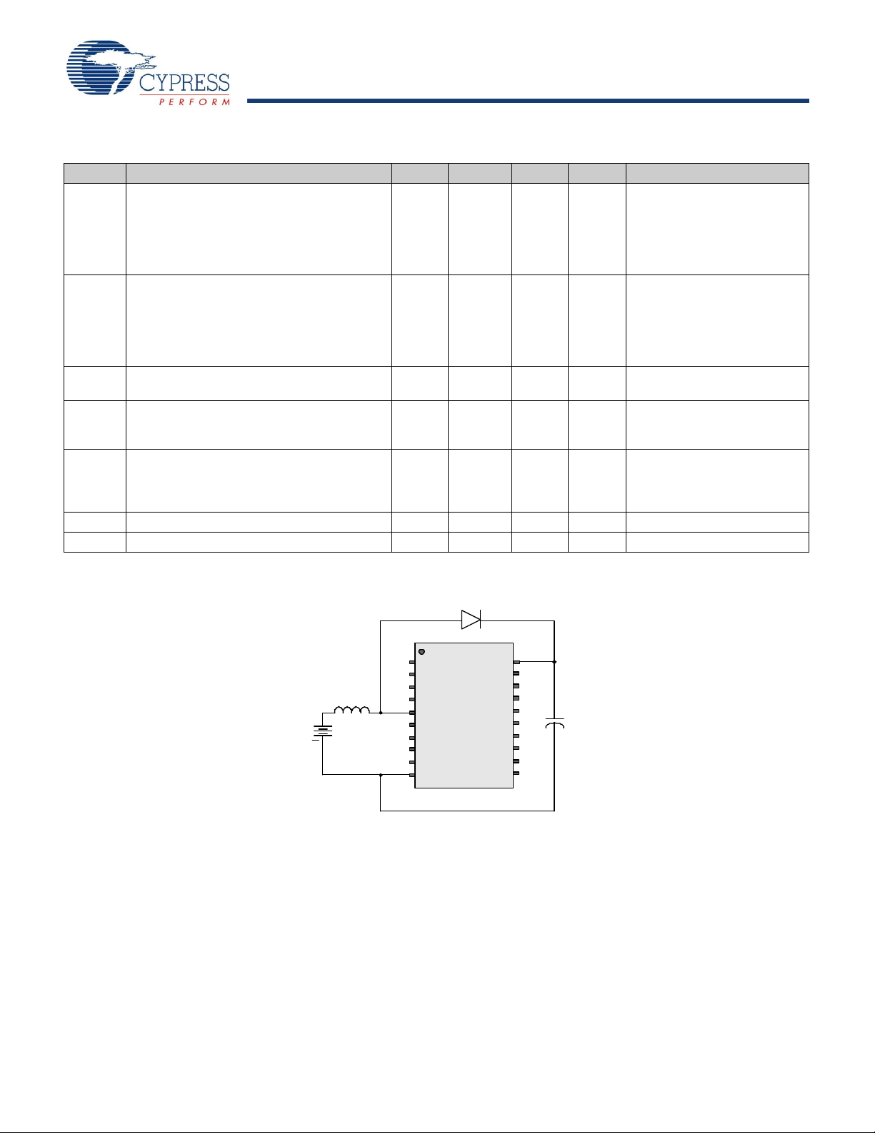
V
PUMP
Note
6. L1 = 2 mH inductor, C1 = 10 mF capacitor, D1 = Schottky diode. See Figure 15.
Symbol Description Min Typ Max Units Notes
ΔV
Line
PUMP_
Line Regulation (over Vi range) – 5 – %VOConfiguration of footnote.
is the “Vdd Value for PUMP
Trip” specified by the VM[2:0]
setting in the DC POR and LVD
Specification, Table 23 on page
24.
ΔV
Load
PUMP_
Load Regulation – 5 – %VOConfiguration of footnote.
is the “Vdd Value for PUMP
Trip” specified by the VM[2:0]
setting in the DC POR and LVD
Specification, Table 23 on page
24.
ΔV
PUMP_
Ripple
E
3
Output Voltage Ripple (depends on cap/load) – 100 – mVpp Configuration of footnote.
Load is 5 mA.
Efficiency 35 50 – % Configuration of footnote.
Load is 5 mA. SMP trip voltage
is set to 3.25V.
E
2
Efficiency 35 80 – % For I load = 1mA, V
2.55V, V
10 uH inductor, 1 uF capacitor,
BAT
= 1.3V,
and Schottky diode.
F
PUMP
DC
PUMP
Switching Frequency – 1.3 – MHz
Switching Duty Cycle – 50 – %
PUMP
[6]
[6]
[6]
[6]
=
VO
VO
Figure 15. Basic Switch Mode Pump Circuit
Document Number: 38-12025 Rev. *O Page 23 of 45
[+] Feedback
Page 24

CY8C21634, CY8C21534
CY8C21434, CY8C21334, CY8C21234
DC Analog Mux Bus Specifications
Notes
7. Always greater than 50 mV above V
PPOR
(PORLEV = 00) for falling supply.
8. Always greater than 50 mV above V
PPOR
(PORLEV = 01) for falling supply.
9. Always greater than 50 mV above V
LVD 0
.
10. Always greater than 50 mV above V
LVD 3
.
Ta bl e 22 lists the guaranteed maximum and minimum specifications for the voltage and temperature ranges: 4.75V to 5.25V and -40°C
≤ T
≤ 85°C, 3.0V to 3.6V and -40°C ≤ TA ≤ 85°C, or 2.4V to 3.0V and -40°C ≤ TA ≤ 85°C, respectively. Typical parameters apply to
A
5V, 3.3V, or 2.7V at 25°C and are for design guidance only.
Table 22. DC Analog Mux Bus Specifications
Symbol Description Min Ty p Max Units Notes
R
R
SW
VDD
Switch Resistance to Common Analog Bus – – 400
WWVdd ≥ 2.7V
800
Resistance of Initialization Switch to Vdd – – 800 W
2.4V ≤ Vdd ≤ 2.7V
DC POR and LVD Specifications
Ta bl e 23 lists the guaranteed maximum and minimum specifications for the voltage and temperature ranges: 4.75V to 5.25V and -40°C
≤ T
≤ 85°C, 3.0V to 3.6V and -40°C ≤ TA ≤ 85°C, or 2.4V to 3.0V and -40°C ≤ TA ≤ 85°C, respectively. Typical parameters apply to
A
5V, 3.3V, or 2.7V at 25°C and are for design guidance only.
Table 23. DC POR and LVD Specifications
Symbol Description Min Ty p Max Units Notes
V
PPOR0
V
PPOR1
V
PPOR2
V
LVD 0
V
LVD 1
V
LVD 2
V
LVD 3
V
LVD 4
V
LVD 5
V
LVD 6
V
LVD 7
V
PUMP0
V
PUMP1
V
PUMP2
V
PUMP3
V
PUMP4
V
PUMP5
V
PUMP6
V
PUMP7
Vdd Value for PPOR Trip
PORLEV[1:0] = 00b
PORLEV[1:0] = 01b
PORLEV[1:0] = 10b
Vdd Value for LVD Trip
VM[2:0] = 000b
VM[2:0] = 001b
VM[2:0] = 010b
VM[2:0] = 011b
VM[2:0] = 100b
VM[2:0] = 101b
VM[2:0] = 110b
VM[2:0] = 111b
Vdd Value for PUMP Trip
VM[2:0] = 000b
VM[2:0] = 001b
VM[2:0] = 010b
VM[2:0] = 011b
VM[2:0] = 100b
VM[2:0] = 101b
VM[2:0] = 110b
VM[2:0] = 111b
–
2.40
2.85
2.95
3.06
4.37
4.50
4.62
4.71
2.45
2.96
3.03
3.18
4.54
4.62
4.71
4.89
2.36
2.82
4.55
2.45
2.92
3.02
3.13
4.48
4.64
4.73
4.81
2.55
3.02
3.10
3.25
4.64
4.73
4.82
5.00
2.40
2.95
4.70
2.51
2.99
3.09
3.20
4.55
4.75
4.83
4.95
2.62
3.09
3.16
3.32
4.74
4.83
4.92
5.12
[7]
[8]
[9]
[10]
Vdd must be greater than or equal
V
to 2.5V during startup, reset from
V
the XRES pin, or reset from
V
Watchdog.
V
V
V
V
V
V
V
V
V
V
V
V
V
V
V
V
Document Number: 38-12025 Rev. *O Page 24 of 45
[+] Feedback
Page 25

CY8C21634, CY8C21534
CY8C21434, CY8C21334, CY8C21234
DC Programming Specifications
Note
11. A maximum of 36 x 50,000 block endurance cycles is allowed. This may be balanced between operations on 36x1 blocks of 50,000 maximum cycles each, 36x2
blocks of 25,000 maximum cycles each, or 36x4 blocks of 12,500 maximum cycles each (to limit the total number of cycles to 36x50,000 and that no single block
ever sees more than 50,000 cycles). For the full industrial range, the user must employ a temperature sensor user module (FlashTemp) and feed the result to
the temperature argument before writing. Refer to the Flash APIs Application Note AN2015 at http://www.cypress.com under Application Notes for more
information.
Ta bl e 24 lists the guaranteed maximum and minimum specifications for the voltage and temperature ranges: 4.75V to 5.25V and -40°C
≤ T
≤ 85°C, 3.0V to 3.6V and -40°C ≤ TA ≤ 85°C, or 2.4V to 3.0V and -40°C ≤ TA ≤ 85°C, respectively. Typical parameters apply to
A
5V, 3.3V, or 2.7V at 25°C and are for design guidance only.
Table 24. DC Programming Specifications
Symbol Description Min Ty p Max Units Notes
Vdd
I
DDP
V
ILP
V
IHP
I
ILP
I
IHP
V
OLV
V
OHV
Flash
Flash
Flash
IWRITE
Supply Voltage for Flash Write Operations 2.70 – – V
Supply Current During Programming or Verify – 5 25 mA
Input Low Voltage During Programming or
– – 0.8 V
Verify
Input High Voltage During Programming or
2.2 – – V
Verify
Input Current when Applying Vilp to P1[0] or
– – 0.2 mA Driving internal pull down resistor.
P1[1] During Programming or Verify
Input Current when Applying Vihp to P1[0] or
– – 1.5 mA Driving internal pull down resistor.
P1[1] During Programming or Verify
Output Low Voltage During Programming or
Verify
Output High Voltage During Programming or
Verify
Flash Endurance (per block) 50,000 – – – Erase/write cycles per block.
ENPB
Flash Endurance (total)
ENT
Flash Data Retention 10 – – Yea rs
DR
[11]
– – Vss +
Vdd -
– Vdd V
1.0
1,800,
– – – Erase/write cycles.
000
0.75
V
Document Number: 38-12025 Rev. *O Page 25 of 45
[+] Feedback
Page 26
CY8C21634, CY8C21534
CY8C21434, CY8C21334, CY8C21234
AC Electrical Characteristics
Notes
12. 4.75V < Vdd < 5.25V.
13. Accuracy derived from Internal Main Oscillator with appropriate trim for Vdd range.
14. 3.0V < Vdd < 3.6V. See Application Note AN2012 “Adjusting PSoC Microcontroller Trims for Dual Voltage-Range Operation” for information on trimming for
operation at 3.3V.
15. See the individual user module data sheets for information on maximum frequencies for user modules.
AC Chip-Level Specifications
The following tables list the guaranteed maximum and minimum specifications for the voltage and temperature ranges: 4.75V to 5.25V
and -40°C ≤ T
apply to 5V, 3.3V, or 2.7V at 25°C and are for design guidance only.
Table 25. 5V and 3.3V AC Chip-Level Specifications
≤ 85°C, 3.0V to 3.6V and -40°C ≤ TA ≤ 85°C, or 2.4V to 3.0V and -40°C ≤ TA ≤ 85°C, respectively. Typical parameters
A
Symbol Description Min Typ Max Units Notes
F
IMO24
Internal Main Oscillator Frequency for 24 MHz 23.4 24 24.6
[12,13,14]
MHz Trimmed for 5V or 3.3V
operation using factory trim
values. See Figure 14 on
page 18. SLIMO mode = 0.
F
IMO6
Internal Main Oscillator Frequency for 6 MHz 5.75 6 6.35
[12,13,14]
MHz Trimmed for 5V or 3.3V
operation using factory trim
values. See Figure 14 on
page 18. SLIMO mode = 1.
F
CPU1
F
CPU2
F
BLK5
F
BLK33
F
32K1
CPU Frequency (5V Nominal) 0.93 24 24.6
CPU Frequency (3.3V Nominal) 0.93 12 12.3
Digital PSoC Block Frequency0(5V Nominal) 0 48 49.2
Digital PSoC Block Frequency (3.3V Nominal) 0 24 24.6
Internal Low Speed Oscillator Frequency 15 32 64 kHz
[12,13]
[13,14]
[12,13,15]
[13,15]
MHz 24 MHz only for SLIMO
mode = 0.
MHz
MHz Refer to the AC Digital Block
Specifications.
MHz
Jitter32k 32 kHz RMS Period Jitter – 100 200 ns
Jitter32k 32 kHz Peak-to-Peak Period Jitter – 1400 –
T
XRST
External Reset Pulse Width 10 – – μs
DC24M 24 MHz Duty Cycle 40 50 60 %
Step24M 24 MHz Trim Step Size – 50 – kHz
Fout48M 48 MHz Output Frequency 46.8 48.0 49.2
[12,14]
MHz Trimmed. Using factory trim
values.
Jitter24M1 24 MHz Peak-to-Peak Period Jitter (IMO) – 600 ps
F
MAX
T
RAMP
Maximum frequency of signal on row input or
– – 12.3 MHz
row output.
Supply Ramp Time 0 – – μs
Document Number: 38-12025 Rev. *O Page 26 of 45
[+] Feedback
Page 27
CY8C21634, CY8C21534
CY8C21434, CY8C21334, CY8C21234
Table 26. 2.7V AC Chip-Level Specifications
Jitter24M1
F
24M
Jitter32k
F
32K1
Notes
16. 2.4V < Vdd < 3.0V.
17. Accuracy derived from Internal Main Oscillator with appropriate trim for Vdd range.
18. See Application Note AN2012 “Adjusting PSoC Microcontroller Trims for Dual Voltage-Range Operation” for information on maximum frequency for user modules.
Symbol Description Min Typ Max Units Notes
F
IMO12
Internal Main Oscillator Frequency for 12 MHz 11.5 12012.7
[16,17,18]
MHz Trimmed for 2.7V operation
using factory trim values.
See Figure 14 on page 18.
SLIMO mode = 1.
F
IMO6
Internal Main Oscillator Frequency for 6 MHz 5.75 6 6.35
[16,17,18]
MHz Trimmed for 2.7V operation
using factory trim values.
See Figure 14 on page 18.
SLIMO mode = 1.
F
CPU1
F
BLK27
F
32K1
CPU Frequency (2.7V Nominal) 0.093 3 3.15
Digital PSoC Block Frequency (2.7V Nominal) 0 12 12.5
Internal Low Speed Oscillator Frequency 8 32 96 kHz
[16,17]
[16,17,18]
MHz 24 MHz only for SLIMO
mode = 0.
MHz Refer to the AC Digital Block
Specifications.
Jitter32k 32 kHz RMS Period Jitter – 150 200 ns
Jitter32k 32 kHz Peak-to-Peak Period Jitter – 1400 –
T
XRST
F
MAX
T
RAMP
External Reset Pulse Width 10 – – μs
Maximum frequency of signal on row input or
– – 12.3 MHz
row output.
Supply Ramp Time 0 – – μs
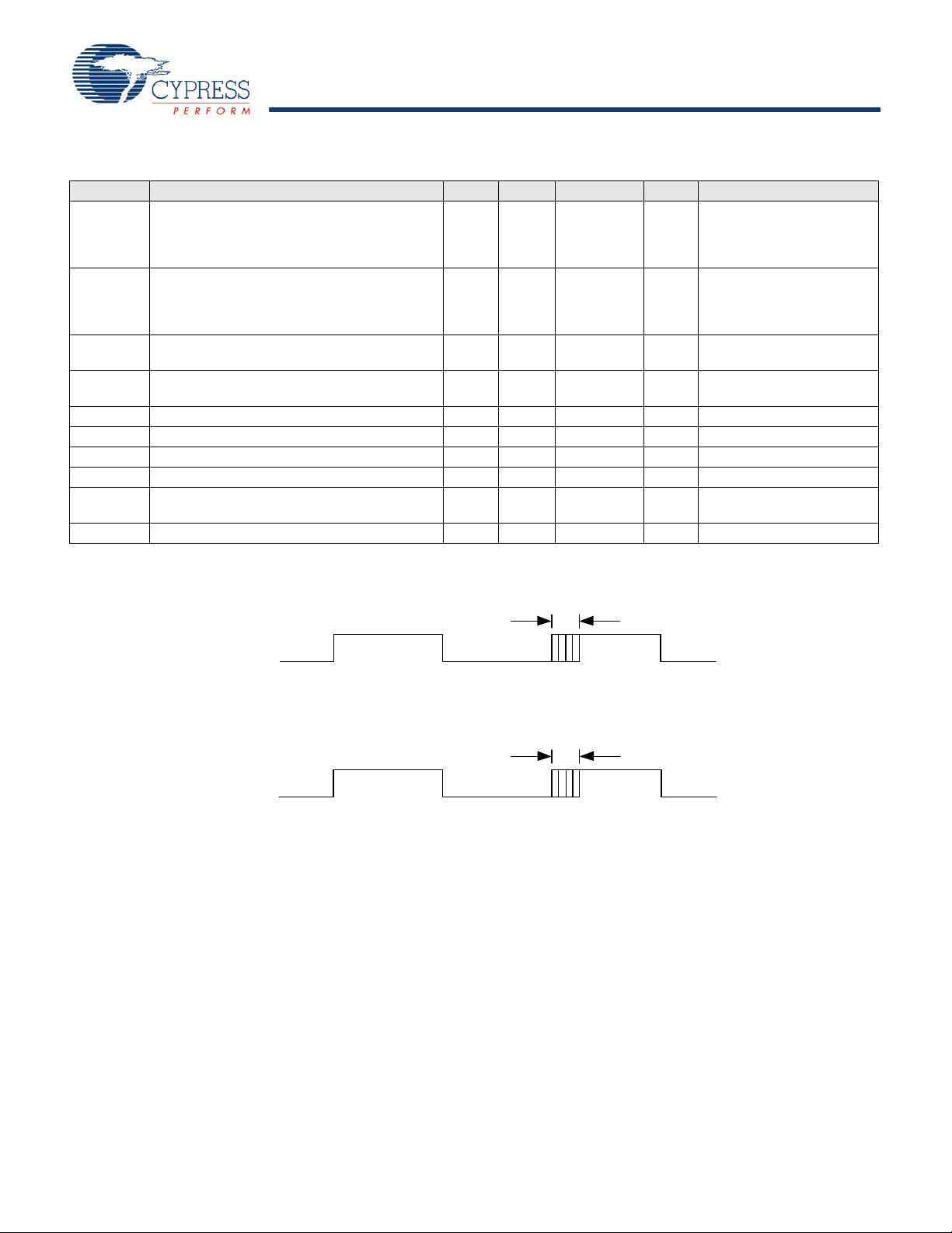
Figure 16. 24 MHz Period Jitter (IMO) Timing Diagram
Figure 17. 32 kHz Period Jitter (ILO) Timing Diagram
Document Number: 38-12025 Rev. *O Page 27 of 45
[+] Feedback
Page 28

CY8C21634, CY8C21534
CY8C21434, CY8C21334, CY8C21234
AC General Purpose IO Specifications
TFallF
TFallS
TRiseF
TRiseS
90%
10%
GPIO
Pin
Output
Voltage
The following tables list the guaranteed maximum and minimum specifications for the voltage and temperature ranges: 4.75V to 5.25V
and -40°C ≤ T
apply to 5V, 3.3V, or 2.7V at 25°C and are for design guidance only.
≤ 85°C, 3.0V to 3.6V and -40°C ≤ TA ≤ 85°C, or 2.4V to 3.0V and -40°C ≤ TA ≤ 85°C, respectively. Typical parameters
A
Table 27. 5V and 3.3V AC GPIO Specifications
Symbol Description Min Typ Max Units Notes
F
GPIO
GPIO Operating Frequency 0 – 12 MHz Normal Strong Mode
TRiseF Rise Time, Normal Strong Mode, Cload = 50 pF 3 – 18 ns Vdd = 4.5 to 5.25V, 10% - 90%
TFallF Fall Time, Normal Strong Mode, Cload = 50 pF 2 – 18 ns Vdd = 4.5 to 5.25V, 10% - 90%
TRiseS Rise Time, Slow Strong Mode, Cload = 50 pF 7 27 – ns Vdd = 3 to 5.25V, 10% - 90%
TFallS Fall Time, Slow Strong Mode, Cload = 50 pF 7 22 – ns Vdd = 3 to 5.25V, 10% - 90%
Table 28. 2.7V AC GPIO Specifications
Symbol Description Min Typ Max Units Notes
F
GPIO
TRiseF Rise Time, Normal Strong Mode, Cload = 50 pF
TFallF Fall Time, Normal Strong Mode, Cload = 50 pF
GPIO Operating Frequency 0 – 3 MHz Normal Strong Mode
6 – 50 ns Vdd = 2.4 to 3.0V, 10% - 90%
6 – 50 ns Vdd = 2.4 to 3.0V, 10% - 90%
TRiseS Rise Time, Slow Strong Mode, Cload = 50 pF 18 40 120 ns Vdd = 2.4 to 3.0V, 10% - 90%
TFallS Fall Time, Slow Strong Mode, Cload = 50 pF
18 40 120 ns Vdd = 2.4 to 3.0V, 10% - 90%
Figure 18. GPIO Timing Diagram
AC Operational Amplifier Specifications
Ta bl e 29 lists the guaranteed maximum and minimum specifications for the voltage and temperature ranges: 4.75V to 5.25V and -40°C
≤ 85°C, 3.0V to 3.6V and -40°C ≤ TA ≤ 85°C, or 2.4V to 3.0V and -40°C ≤ TA ≤ 85°C, respectively. Typical parameters apply to
≤ T
A
5V, 3.3V, or 2.7V at 25°C and are for design guidance only.
Table 29. AC Operational Amplifier Specifications
Symbol Description Min Ty p Max Units Notes
T
COMP
Comparator Mode Response Time, 50 mV
Overdrive
100
200
nsnsVdd ≥ 3.0V.
2.4V < Vcc < 3.0V.
AC Low Power Comparator Specifications
Ta bl e 30 lists the guaranteed maximum and minimum specifications for the voltage and temperature ranges: 4.75V to 5.25V and -40°C
≤ T
≤ 85°C, 3.0V to 3.6V and -40°C ≤ TA ≤ 85°C, or 2.4V to 3.0V and -40°C ≤ TA ≤ 85°C, respectively. Typical parameters apply to
A
5V at 25°C and are for design guidance only.
Table 30. AC Low Power Comparator Specifications
Symbol Description Min Typ Max Units Notes
T
RLPC
Document Number: 38-12025 Rev. *O Page 28 of 45
LPC response time – – 50 μs ≥ 50 mV overdrive comparator
reference set within V
REFLPC
.
[+] Feedback
Page 29
CY8C21634, CY8C21534
CY8C21434, CY8C21334, CY8C21234
AC Analog Mux Bus Specifications
Note
19. 50 ns minimum input pulse width is based on the input synchronizers running at 12 MHz (84 ns nominal period).
Ta bl e 31 lists the guaranteed maximum and minimum specifications for the voltage and temperature ranges: 4.75V to 5.25V and -40°C
≤ T
≤ 85°C, 3.0V to 3.6V and -40°C ≤ TA ≤ 85°C, or 2.4V to 3.0V and -40°C ≤ TA ≤ 85°C, respectively. Typical parameters apply to
A
5V, 3.3V, or 2.7V at 25°C and are for design guidance only.
Table 31. AC Analog Mux Bus Specifications
Symbol Description Min Ty p Max Units Notes
F
SW
Switch Rate – – 3.17 MHz
AC Digital Block Specifications
The following tables list the guaranteed maximum and minimum specifications for the voltage and temperature ranges: 4.75V to 5.25V
and -40°C ≤ TA ≤ 85°C, 3.0V to 3.6V and -40°C ≤ TA ≤ 85°C, or 2.4V to 3.0V and -40°C ≤ TA ≤ 85°C, respectively. Typical parameters
apply to 5V, 3.3V, or 2.7V at 25°C and are for design guidance only.
Table 32. 5V and 3.3V AC Digital Block Specifications
Function Description Min Typ Max Units Notes
All
Functions
Timer Capture Pulse Width 50
Maximum Block Clocking Frequency (> 4.75V) 49.2 MHz 4.75V < Vdd < 5.25V.
Maximum Block Clocking Frequency (< 4.75V) 24.6 MHz 3.0V < Vdd < 4.75V.
[19]
– – ns
Maximum Frequency, No Capture – – 49.2 MHz 4.75V < Vdd < 5.25V.
Maximum Frequency, With or Without Capture – – 24.6 MHz
Counter Enable Pulse Width 50 – – ns
Maximum Frequency, No Enable Input – – 49.2 MHz 4.75V < Vdd < 5.25V.
Maximum Frequency, Enable Input – – 24.6 MHz
Dead Band Kill Pulse Width:
Asynchronous Restart Mode 20 – – ns
Synchronous Restart Mode 50 – – ns
Disable Mode 50 – – ns
Maximum Frequency – – 49.2 MHz 4.75V < Vdd < 5.25V.
CRCPRS
Maximum Input Clock Frequency – – 49.2 MHz 4.75V < Vdd < 5.25V.
(PRS
Mode)
CRCPRS
Maximum Input Clock Frequency – – 24.6 MHz
(CRC
Mode)
SPIM Maximum Input Clock Frequency – – 8.2 MHz Maximum data rate at 4.1 MHz
due to 2 x over clocking.
SPIS Maximum Input Clock Frequency – – 4.1 MHz
Width of SS_ Negated Between Transmissions 50 – – ns
Transmitter Maximum Input Clock Frequency
–
–
24.6
MHz
Maximum data rate at 3.08 MHz
due to 8 x over clocking.
Maximum Input Clock Frequency with Vdd ≥
4.75V, 2 Stop Bits
Receiver Maximum Input Clock Frequency
–
–
–
–
49.2
24.6
MHz
MHz
Maximum data rate at 6.15 MHz
due to 8 x over clocking.
Maximum data rate at 3.08 MHz
due to 8 x over clocking.
Maximum Input Clock Frequency with Vdd ≥
4.75V, 2 Stop Bits
–
–
49.2
MHz
Maximum data rate at 6.15 MHz
due to 8 x over clocking.
Document Number: 38-12025 Rev. *O Page 29 of 45
[+] Feedback
Page 30
CY8C21634, CY8C21534
CY8C21434, CY8C21334, CY8C21234
Table 33. 2.7V AC Digital Block Specifications
Note
20. 100 ns minimum input pulse width is based on the input synchronizers running at 12 MHz (84 ns nominal period).
Function Description Min Typ Max Units Notes
All
Maximum Block Clocking Frequency 12.7 MHz 2.4V < Vdd < 3.0V.
Functions
Timer Capture Pulse Width 100
[20]
– – ns
Maximum Frequency, With or Without Capture – – 12.7 MHz
Counter Enable Pulse Width 100 – – ns
Maximum Frequency, No Enable Input – – 12.7 MHz
Maximum Frequency, Enable Input – – 12.7 MHz
Dead Band Kill Pulse Width:
Asynchronous Restart Mode 20 – – ns
Synchronous Restart Mode 100 – – ns
Disable Mode 100 – – ns
Maximum Frequency – – 12.7 MHz
CRCPRS
Maximum Input Clock Frequency – – 12.7 MHz
(PRS
Mode)
CRCPRS
Maximum Input Clock Frequency – – 12.7 MHz
(CRC
Mode)
SPIM Maximum Input Clock Frequency – – 6.35 MHz Maximum data rate at 3.17 MHz
due to 2 x over clocking.
SPIS Maximum Input Clock Frequency – – 4.1 MHz
Width of SS_ Negated Between Transmissions 100 – – ns
Transmitter Maximum Input Clock Frequency – – 12.7 MHz Maximum data rate at 1.59 MHz
due to 8 x over clocking.
Receiver Maximum Input Clock Frequency – – 12.7 MHz Maximum data rate at 1.59 MHz
due to 8 x over clocking.
AC External Clock Specifications
The following tables list the guaranteed maximum and minimum specifications for the voltage and temperature ranges: 4.75V to 5.25V
and -40°C ≤ T
and are for design guidance only.
≤ 85°C, or 3.0V to 3.6V and -40°C ≤ TA ≤ 85°C, respectively. Typical parameters apply to 5V, 3.3V, or 2.7V at 25°C
A
Table 34. 5V AC External Clock Specifications
Symbol Description Min Typ Max Units
F
OSCEXT
Frequency 0.093 –24.6MHz
– High Period 20.6
– Low Period 20.6
– Power Up IMO to Switch 150
Document Number: 38-12025 Rev. *O Page 30 of 45
– 5300 ns
– –ns
– – μs
[+] Feedback
Page 31
CY8C21634, CY8C21534
CY8C21434, CY8C21334, CY8C21234
Table 35. 3.3V AC External Clock Specifications
Symbol Description Min Typ Max Units Notes
F
OSCEXT
Frequency with CPU Clock divide by 1 0.093 – 12.3 MHz Maximum CPU frequency is 12
MHz at 3.3V. With the CPU clock
divider set to 1, the external clock
must adhere to the maximum
frequency and duty cycle
requirements.
F
OSCEXT
Frequency with CPU Clock divide by 2 or
greater
0.186 – 24.6 MHz If the frequency of the external clock
is greater than 12 MHz, the CPU
clock divider must be set to 2 or
greater. In this case, the CPU clock
divider ensures that the fifty percent
duty cycle requirement is met.
– High Period with CPU Clock divide by 1 41.7
– Low Period with CPU Clock divide by 1 41.7
– Power Up IMO to Switch 150
– 5300 ns
– –ns
– – μs
Table 36. 2.7V AC External Clock Specifications
Symbol Description Min Ty p Max Units Notes
F
OSCEXT
Frequency with CPU Clock divide by 1 0.093 –3.080MHz Maximum CPU frequency is 3 MHz
at 2.7V. With the CPU clock divider
set to 1, the external clock must
adhere to the maximum frequency
and duty cycle requirements.
F
OSCEXT
Frequency with CPU Clock divide by 2 or
greater
0.186 – 6.35 MHz If the frequency of the external clock
is greater than 3 MHz, the CPU
clock divider must be set to 2 or
greater. In this case, the CPU clock
divider ensures that the fifty percent
duty cycle requirement is met.
– High Period with CPU Clock divide by 1 160
– 5300 ns
– Low Period with CPU Clock divide by 1 160 – –ns
– Power Up IMO to Switch 150
– – μs
AC Programming Specifications
Ta bl e 37 lists the guaranteed maximum and minimum specifications for the voltage and temperature ranges: 4.75V to 5.25V and -40°C
≤ T
≤ 85°C, or 3.0V to 3.6V and -40°C ≤ TA ≤ 85°C, respectively. Typical parameters apply to 5V, 3.3V, or 2.7V at 25°C and are for
A
design guidance only.
Table 37. AC Programming Specifications
Symbol Description Min Typ Max Units Notes
T
RSCLK
T
FSCLK
T
SSCLK
T
HSCLK
F
SCLK
T
ERASEB
Document Number: 38-12025 Rev. *O Page 31 of 45
Rise Time of SCLK 1 – 20 ns
Fall Time of SCLK 1 – 20 ns
Data Set up Time to Falling Edge of SCLK 40 – – ns
Data Hold Time from Falling Edge of SCLK 40 – – ns
Frequency of SCLK 0 – 8 MHz
Flash Erase Time (Block) – 15 – ms
[+] Feedback
Page 32

CY8C21634, CY8C21534
CY8C21434, CY8C21334, CY8C21234
Table 37. AC Programming Specifications (continued)
Note
21. A Fast-Mode I2C-bus device may be used in a Standard-Mode I2C-bus system, but the requirement t
SU;DAT
≥ 250 ns must then be met. This is automatically
the case if the device does not stretch the LOW period of the SCL signal. If such device does stretch the LOW period of the SCL signal, it must output the next
data bit to the SDA line t
rmax
+ t
SU;DAT
= 1000 + 250 = 1250 ns (according to the Standard-Mode I2C-bus specification) before the SCL line is released.
Symbol Description Min Typ Max Units Notes
T
WRITE
T
DSCLK
T
DSCLK3
T
DSCLK2
2
C Specifications
AC I
Flash Block Write Time – 30 – ms
Data Out Delay from Falling Edge of SCLK – – 45 ns 3.6 < Vdd
Data Out Delay from Falling Edge of SCLK – – 50 ns 3.0 ≤ Vdd ≤ 3.6
Data Out Delay from Falling Edge of SCLK – – 70 ns 2.4 ≤ Vdd ≤ 3.0
The following tables list the guaranteed maximum and minimum specifications for the voltage and temperature ranges: 4.75V to 5.25V
and -40°C ≤ T
apply to 5V, 3.3V, or 2.7V at 25°C and are for design guidance only.
≤ 85°C, 3.0V to 3.6V and -40°C ≤ TA ≤ 85°C, or 2.4V to 3.0V and -40°C ≤ TA ≤ 85°C, respectively. Typical parameters
A
Table 38. AC Characteristics of the I2C SDA and SCL Pins for Vdd ≥ 3.0V
Symbol Description
F
SCLI2C
T
HDSTAI2C
SCL Clock Frequency 0 100 0 400 kHz
Hold Time (repeated) START Condition.
After this period, the first clock pulse is
Standard Mode Fast Mode
Min Max Min Max
4.0
–0.6– μs
Units
generated.
T
LOWI2C
T
HIGHI2C
T
SUSTAI2C
T
HDDATI2C
T
SUDATI2C
T
SUSTOI2C
T
BUFI2C
T
SPI2C
LOW Period of the SCL Clock 4.7 –1.3– μs
HIGH Period of the SCL Clock 4.0 –0.6– μs
Set-up Time for a Repeated START
4.7 –0.6– μs
Condition
Data Hold Time 0 –0– μs
Data Set-up Time 250 – 100
[21]
–ns
Set-up Time for STOP Condition 4.0 –0.6– μs
Bus Free Time Between a STOP and START
4.7 –1.3– μs
Condition
Pulse Width of spikes are suppressed by the
– – 0 50 ns
input filter.
Document Number: 38-12025 Rev. *O Page 32 of 45
[+] Feedback
Page 33

CY8C21634, CY8C21534
CY8C21434, CY8C21334, CY8C21234
Table 39. 2.7V AC Characteristics of the I
SDA
SCL
S
Sr SP
T
BUF I2C
T
SPI2C
T
HDSTAI2C
T
SUSTOI2C
T
SUSTAI2C
T
LOWI2C
T
HIGHI2C
T
HDDATI2C
T
HDSTAI2C
T
SUDATI2C
Symbol Description
F
SCLI2C
T
HDSTAI2C
SCL Clock Frequency 0 100 – – kHz
Hold Time (repeated) START Condition.
After this period, the first clock pulse is
generated.
T
LOWI2C
T
HIGHI2C
T
SUSTAI2C
T
HDDATI2C
T
SUDATI2C
T
SUSTOI2C
T
BUFI2C
T
SPI2C
LOW Period of the SCL Clock 4.7 – – – μs
HIGH Period of the SCL Clock 4.0 – – – μs
Set up Time for a Repeated START
Condition
Data Hold Time 0 – – – μs
Data Set-up Time 250 – – –ns
Set up Time for STOP Condition 4.0 – – – μs
Bus Free Time Between a STOP and START
Condition
Pulse Width of spikes are suppressed by the
input filter.
Figure 19. Definition for Timing for Fast/Standard Mode on the I
2
C SDA and SCL Pins (Fast Mode not Supported)
Standard Mode Fast Mode
Min Max Min Max
4.0 – – – μs
4.7 – – – μs
4.7 ––– μs
– –––ns
2
C Bus
Units
Document Number: 38-12025 Rev. *O Page 33 of 45
[+] Feedback
Page 34

CY8C21634, CY8C21534
CY8C21434, CY8C21334, CY8C21234
Packaging Information
PIN 1 ID
0°~8°
18
916
SEATING PLANE
0.230[5.842]
0.244[6.197]
0.157[3.987]
0.150[3.810]
0.386[9.804]
0.393[9.982]
0.050[1.270]
BSC
0.061[1.549]
0.068[1.727]
0.004[0.102]
0.0098[0.249]
0.0138[0.350]
0.0192[0.487]
0.016[0.406]
0.035[0.889]
0.0075[0.190]
0.0098[0.249]
DIMENSIONS IN INCHES[MM] MIN.
MAX.
0.016[0.406]
0.010[0.254]
X 45°
0.004[0.102]
REFERENCE JEDEC MS-012
PART #
S16.15 STANDARD PKG.
SZ16.15 LEAD FREE PKG.
PACKAGE WEIGHT 0.15gms
51-85068 *B
51-85077 *C
This section shows the packaging specifications for the CY8C21x34 PSoC device with the thermal impedances for each package.
Important Note Emulation tools may require a larger area on the target PCB than the chip’s footprint. For a detailed description of
the emulation tools’ dimensions, refer to the document titled PSoC Emulator Pod Dimensions at
http://www.cypress.com/design/MR10161.
Packaging Dimensions
Figure 20. 16-Pin (150-Mil) SOIC
Figure 21. 20-Pin (210-MIL) SSOP
Document Number: 38-12025 Rev. *O Page 34 of 45
[+] Feedback
Page 35

CY8C21634, CY8C21534
CY8C21434, CY8C21334, CY8C21234
Figure 22. 28-Pin (210-Mil) SSOP
51-85079 *C
51-85188 *B
E-PAD X, Y for this product is 3.53 mm, 3.53 mm (+/-0.11 mm)
Figure 23. 32-Pin (5x5 mm 0.93 MAX) QFN
Document Number: 38-12025 Rev. *O Page 35 of 45
[+] Feedback
Page 36

CY8C21634, CY8C21534
CY8C21434, CY8C21334, CY8C21234
Figure 24. 32-Pin (5x5 mm 0.60 MAX) QFN
E-PAD X, Y for this product is 3.53 mm, 3.53 mm (+/-0.11 mm)
001-06392 *A
001-44368 *A
Figure 25. 32-Pin (5 X 5 X 0.4MM) QFN (SAWN 1.85 X 2.85 EPAD
Document Number: 38-12025 Rev. *O Page 36 of 45
[+] Feedback
Page 37

CY8C21634, CY8C21534
CY8C21434, CY8C21334, CY8C21234
Figure 26. 32-Pin Sawn QFN Package
001-30999 *A
001-42168 *C
Figure 27. 32-Pin Thin Sawn QFN Package
Important Note For information on the preferred dimensions for mounting QFN packages, see the following Application Note at
http://www.amkor.com/products/notes_papers/MLFAppNote.pdf.
Document Number: 38-12025 Rev. *O Page 37 of 45
[+] Feedback
Page 38

CY8C21634, CY8C21534
CY8C21434, CY8C21334, CY8C21234
Thermal Impedances
51-85062 *C
Figure 28. 56-Pin (300-Mil) SSOP
Table 40. Thermal Impedances per Package
Package Typica l θJA
16 SOIC 123 oC/W 55 oC/W
20 SSOP 117 oC/W 41 oC/W
28 SSOP 96 oC/W 39 oC/W
32 QFN
32 QFN
[23]
5x5 mm 0.60 MAX 27 oC/W 15 oC/W
[23]
5x5 mm 0.93 MAX 22 oC/W 12 oC/W
[22]
Typical θ
JC
Document Number: 38-12025 Rev. *O Page 38 of 45
[+] Feedback
Page 39

CY8C21634, CY8C21534
CY8C21434, CY8C21334, CY8C21234
Solder Reflow Peak Temperature
Notes
22. TJ = TA + Power x θ
JA
23. To achieve the thermal impedance specified for the QFN package, the center thermal pad must be soldered to the PCB ground plane
24. Higher temperatures may be required based on the solder melting point. Typical temperatures for solder are 220 ± 5
o
C with Sn-Pb or 245 ± 5oC with Sn-Ag-Cu
paste. Refer to the solder manufacturer specifications.
Following is the minimum solder reflow peak temperature to achieve good solderability.
Table 41. Solder Reflow Peak Temperature
Package Minimum Peak Temperature
16 SOIC 240oC 260oC
20 SSOP 240oC 260oC
28 SSOP 240oC 260oC
32 QFN 240oC 260oC
[24]
Maximum Peak Temperature
Document Number: 38-12025 Rev. *O Page 39 of 45
[+] Feedback
Page 40

CY8C21634, CY8C21534
CY8C21434, CY8C21334, CY8C21234
Development Tool Selection
This section presents the development tools available for all
current PSoC device families including the CY8C21x34 family.
Software
PSoC Designer
At the core of the PSoC development software suite is PSoC
Designer. Used by thousands of PSoC developers, this robust
software has been facilitating PSoC designs for half a decade.
PSoC Designer is available free of charge at
http://www.cypress.com under DESIGN RESOURCES >>
Software and Drivers.
PSoC Programmer
Flexible enough to be used on the bench in development, yet
suitable for factory programming, PSoC Programmer works
either as a standalone programming application or operates
directly from PSoC Designer or PSoC Express. PSoC
Programmer software is compatible with both PSoC ICE-Cube
In-Circuit Emulator and PSoC MiniProg. PSoC programmer is
available free ofcharge at http://www.cypress.com/psocpro-
grammer.
C Compilers
PSoC Designer comes with a free HI-TECH C Lite C compiler.
The HI-TECH C Lite compiler is free, supports all PSoC devices,
integrates fully with PSoC Designer and PSoC Express, and
runs on Windows versions up to 32-bit Vista. Compilers with
additional features are available at additional cost from their
manufactures.
■ HI-TECH C PRO for the PSoC is available from
http://www.htsoft.com.
■ ImageCraft Cypress Edition Compiler is available from
http://www.imagecraft.com.
Development Kits
All development kits can be purchased from the Cypress Online
Store.
CY3215-DK Basic Development Kit
The CY3215-DK is for prototyping and development with PSoC
Designer. This kit supports in-circuit emulation and the software
interface allows users to run, halt, and single step the processor
and view the content of specific memory locations. Advance
emulation features also supported through PSoC Designer. The
kit includes:
■ PSoC Designer Software CD
■ ICE-Cube In-Circuit Emulator
■ ICE Flex-Pod for CY8C29x66 Family
■ Cat-5 Adapter
■ Mini-Eval Programming Board
™
■ 110 ~ 240V Power Supply, Euro-Plug Adapter
■ iMAGEcraft C Compiler (Registration Required)
■ ISSP Cable
■ USB 2.0 Cable and Blue Cat-5 Cable
■ 2 CY8C29466-24PXI 28-PDIP Chip Samples
CY3210-ExpressDK PSoC Express Development Kit
The CY3210-ExpressDK is for advanced prototyping and
development with PSoC Express (may be used with ICE-Cube
In-Circuit Emulator). It provides access to I
2
C buses, voltage
reference, switches, upgradeable modules and more. The kit
includes:
■ PSoC Express Software CD
■ Express Development Board
■ 4 Fan Modules
■ 2 Proto Modules
■ MiniProg In-System Serial Programmer
■ MiniEval PCB Evaluation Board
■ Jumper Wire Kit
■ USB 2.0 Cable
■ Serial Cable (DB9)
■ 110 ~ 240V Power Supply, Euro-Plug Adapter
■ 2 CY8C24423A-24PXI 28-PDIP Chip Samples
■ 2 CY8C27443-24PXI 28-PDIP Chip Samples
■ 2 CY8C29466-24PXI 28-PDIP Chip Samples
Evaluation Tools
All evaluation tools can be purchased from the Cypress Online
Store.
CY3210-MiniProg1
The CY3210-MiniProg1 kit allows a user to program PSoC
devices through the MiniProg1 programming unit. The MiniProg
is a small, compact prototyping programmer that connects to the
PC through a provided USB 2.0 cable. The kit includes:
■ MiniProg Programming Unit
■ MiniEval Socket Programming and Evaluation Board
■ 28-Pin CY8C29466-24PXI PDIP PSoC Device Sample
■ 28-Pin CY8C27443-24PXI PDIP PSoC Device Sample
■ PSoC Designer Software CD
■ Getting Started Guide
■ USB 2.0 Cable
Document Number: 38-12025 Rev. *O Page 40 of 45
[+] Feedback
Page 41

CY8C21634, CY8C21534
CY8C21434, CY8C21334, CY8C21234
CY3210-PSoCEval1
Notes
25. Flex-Pod kit includes a practice flex-pod and a practice PCB, in addition to two flex-pods.
26. Foot kit includes surface mount feet that can be soldered to the target PCB.
The CY3210-PSoCEval1 kit features an evaluation board and
the MiniProg1 programming unit. The evaluation board includes
Device Programmers
All device programmers can be purchased from the Cypress
Online Store.
an LCD module, potentiometer, LEDs, and plenty of breadboarding space to meet all of your evaluation needs. The kit
includes:
■ Evaluation Board with LCD Module
■ MiniProg Programming Unit
■ 28-Pin CY8C29466-24PXI PDIP PSoC Device Sample (2)
■ PSoC Designer Software CD
■ Getting Started Guide
■ USB 2.0 Cable
CY3214-PSoCEvalUSB
The CY3214-PSoCEvalUSB evaluation kit features a
CY3216 Modular Programmer
The CY3216 Modular Programmer kit features a modular
programmer and the MiniProg1 programming unit. The modular
programmer includes three programming module cards and
supports multiple Cypress products. The kit includes:
■ Modular Programmer Base
■ 3 Programming Module Cards
■ MiniProg Programming Unit
■ PSoC Designer Software CD
■ Getting Started Guide
■ USB 2.0 Cable
development board for the CY8C24794-24LFXI PSoC device.
Special features of the board include both USB and capacitive
sensing development and debugging support. This evaluation
board also includes an LCD module, potentiometer, LEDs, an
enunciator and plenty of bread boarding space to meet all of your
evaluation needs. The kit includes:
■ PSoCEvalUSB Board
■ LCD Module
■ MIniProg Programming Unit
■ Mini USB Cable
■ PSoC Designer and Example Projects CD
■ Getting Started Guide
■ Wire Pack
CY3207ISSP In-System Serial Programmer (ISSP)
The CY3207ISSP is a production programmer. It includes
protection circuitry and an industrial case that is more robust than
the MiniProg in a production-programming environment.
Note CY3207ISSP needs special software and is not compatible
with PSoC Programmer. The kit includes:
■ CY3207 Programmer Unit
■ PSoC ISSP Software CD
■ 110 ~ 240V Power Supply, Euro-Plug Adapter
■ USB 2.0 Cable
Accessories (Emulation and Programming)
Table 42. Emulation and Programming Accessories
Part # Pin Package Flex-Pod Kit
[25]
Foot Kit
CY8C21234-24S 16 SOIC CY3250-21X34 CY3250-16SOIC-FK Programming adapter converts
CY8C21334-24PVXI 20 SSOP CY3250-21X34 CY3250-20SSOP-FK
CY8C21434-24LFXI 32 QFN CY3250-21X34QFN CY3250-32QFN-FK
CY8C21534-24PVXI 28 SSOP CY3250-21X34 CY3250-28SSOP-FK
CY8C21634-24LFXI 32 QFN CY3250-21X34QFN CY3250-32QFN-FK
[26]
Adapter
non-DIP package to DIP
footprint. Specific details and
ordering information for each of
the adapters can be found at
http://www.emulation.com.
Third-Party Tools
Several tools have been specially designed by the following
3rd-party vendors to accompany PSoC devices during development and production. Specific details for each of these tools
can be found at http://www.cypress.com under DESIGN
RESOURCES >> Evaluation Boards.
Document Number: 38-12025 Rev. *O Page 41 of 45
Build a PSoC Emulator into Your Board
For details on how to emulate your circuit before going to volume
production using an on-chip debug (OCD) non-production PSoC
device, see Application Note AN2323 “Debugging - Build a PSoC
Emulator into Your Board”.
[+] Feedback
Page 42
CY8C21634, CY8C21534
CY8C21434, CY8C21334, CY8C21234
Ordering Information
Notes
27. All Digital IO Pins also connect to the common analog mux.
28. Refer to the section 32-Pin Part Pinout on page 11 for pin differences.
a
Package
Code
Ordering
Flash
SRAM
(Bytes)
Pump
(Bytes)
Switch Mode
Range
Temperature
Digital
Blocks
Analog
Blocks
Pins
Digital IO
16 Pin (150-Mil) SOIC CY8C21234-24SXI 8K 512 Ye s -40°C to +85°C 4 4 12 12
16 Pin (150-Mil) SOIC
CY8C21234-24SXIT 8K 512 Ye s -40°C to +85°C 4 4 12 12
(Tape and Reel)
20 Pin (210-Mil) SSOP CY8C21334-24PVXI 8K 512 No -40°C to +85°C 4 4 16 16
20 Pin (210-Mil) SSOP
CY8C21334-24PVXIT 8K 512 No -40°C to +85°C 4 4 16 16
(Tape and Reel)
28 Pin (210-Mil) SSOP CY8C21534-24PVXI 8K 512 No -40°Cto +85°C 4 4 24 24
28 Pin (210-Mil) SSOP
CY8C21534-24PVXIT 8K 512 No -40°C to +85°C 4 4 24 24
(Tape and Reel)
32 Pin (5x5 mm 0.93 MAX)
[27]
QFN
32 Pin (5x5 mm 0.93 MAX) QFN
CY8C21434-24LFXI 8K 512 No -40°C to +85°C 4 4 28 28
CY8C21434-24LFXIT 8K 512 No -40°C to +85°C 4 4 28 28
b (Tape and Reel)
32 Pin (5x5 mm 0.60 MAX) QFN
[28]
32 Pin (5x5 mm 0.60 MAX) QFN
[28]
(Tape and Reel)
32 Pin (5x5 mm 0.93 MAX) QFN
[28]
32 Pin (5x5 mm 0.93 MAX) QFN
[28]
(Tape and Reel)
32 Pin (5x5 mm 1.00 MAX)
CY8C21434-24LKXI 8K 512 No -40°C to +85°C 4 4 28 28
CY8C21434-24LKXIT 8K 512 No -40°C to +85°C 4 4 28 28
CY8C21634-24LFXI 8K 512 Ye s -40°C to +85°C 4 4 26 26
CY8C21634-24LFXIT 8K 512 Yes -40°C to +85°C 4 4 26 26
CY8C21434-24LTXI 8K 512 No -40°C to +85°C 4 4 28 28
SAWN QFN
32 Pin (5x5 mm 1.00 MAX)
SAWN QFN
[28]
(Tape and
CY8C21434-24LTXIT 8K 512 No -40°C to +85°C 4 4 28 28
Reel)
32 Pin (5x5 mm 0.40 MAX)
SAWN QFN
32 Pin (5x5 mm 0.40 MAX)
SAWN QFN
[28]
[28]
CY8C21434-24LCXI 8K 512 No -40°C to +85°C 4 4 28 28
CY8C21434-24LCXIT 8K 512 No -40°C to +85°C 4 4 28 28
(Tape and Reel)
32 Pin (5x5 mm 0.60 MAX)
CY8C21434-24LQXI 8K 512 No -40°C to +85°C 4 4 28 28
THIN SAWN QFN
32 Pin (5x5 mm 0.60 MAX)
CY8C21434-24LQXIT 8K 512 No -40°C to +85°C 4 4 28 28
THIN SAWN QFN
(Tape and Reel)
32 Pin (5x5 mm 0.93 MAX)
SAWN QFN
32 Pin (5x5 mm 0.93 MAX)
SAWN QFN
[28]
[28]
CY8C21634-24LTXI 8K 512 Ye s -40°C to +85°C 4 4 26 26
CY8C21634-24LTXIT 8K 512 Ye s -40°C to +85°C 4 4 26 26
(Tape and Reel)
56 Pin OCD SSOP CY8C21001-24PVXI 8K 512 Ye s -40°C to +85°C 4 4 26 26
Analog
Inputs
[27]
0 No
[27]
0 No
[27]
0 Ye s
[27]
0 Ye s
[27]
0 Ye s
[27]
0 Ye s
[27]
0 Ye s
[27]
0 Ye s
[27]
0 Ye s
[27]
0 Ye s
[27]
0 Ye s
[27]
0 Ye s
[27]
0 Ye s
[27]
0 Ye s
a
0 Ye s
a
0 Ye s
[27]
0 Ye s
[27]
0 Ye s
[27]
0 Ye s
[27]
0 Ye s
[27]
0 Ye s
Analog
Outputs
XRES Pin
Note For Die sales information, contact a local Cypress sales office or Field Applications Engineer (FAE).
Document Number: 38-12025 Rev. *O Page 42 of 45
[+] Feedback
Page 43
CY8C21634, CY8C21534
CY8C21434, CY8C21334, CY8C21234
Ordering Code Definitions
CY 8 C 21 xxx-24xx
Package Type: Thermal Rating:
PX = PDIP Pb-Free C = Commercial
SX = SOIC Pb-Free I = Industrial
PVX = SSOP Pb-Free E = Extended
LFX/LKX = QFN Pb-Free
AX = TQFP Pb-Free
Speed: 24 MHz
Part Number
Family Code
Technology Code: C = CMOS
Marketing Code: 8 = Cypress PSoC
Company ID: CY = Cypress
Document Number: 38-12025 Rev. *O Page 43 of 45
[+] Feedback
Page 44

CY8C21634, CY8C21534
CY8C21434, CY8C21334, CY8C21234
Document History Page
Document Title: CY8C21234/CY8C21334/CY8C21434/CY8C21534/CY8C21634 PSoC® Programmable System-on-Chip™
Document Number: 38-12025
Revision ECN No.
** 227340 HMT See ECN New silicon and document (Revision **).
*A 235992 SFV See ECN Updated Overview and Electrical Spec. chapters, along with revisions to the
*B 248572 SFV See ECN Changed title to include all part #s. Changed 28-pin SSOP from CY8C21434
*C 277832 HMT See ECN Verify data sheet standards from SFV memo. Add Analog Input Mux to appli-
*D 285293 HMT See ECN Update 2.7V DC GPIO spec. Add Reflow Peak Temp. table.
*E 301739 HMT See ECN DC Chip-Level Specification changes. Update links to new CY.com Portal.
*F 329104 HMT See ECN Re-add pinout ISSP notation. Fix TMP register names. Clarify ADC feature.
*G 352736 HMT See ECN Add new color and logo. Add URL to preferred dimensions for mounting MLF
*H 390152 HMT See ECN Clarify MLF thermal pad connection info. Replace 16-pin 300-MIL SOIC with
*I 413404 HMT See ECN Update 32-pin QFN E-Pad dimensions and rev. *A. Update CY branding and
*J 430185 HMT See ECN Add new 32-pin 5x5 mm 0.60 thickness QFN package and diagram,
*K 677717 HMT See ECN Add CapSense SNR requirement reference. Add new Dev. Tool section. Add
*L 2147847 UVS/PYRS 02/27/08 Added 32-Pin QFN Sawn pin diagram, package diagram, and ordering infor-
*M 2273246 UVS/AESA 04/01/08 Added 32 pin thin sawn package diagram.
*N 2618124 OGNE/PYRS 12/09/08 Added Note in Ordering Information section.
*O 2684145 SNV/AESA 04/06/2009 Updated 32-Pin Sawn QFN package dimension for CY8C21434-24LTXIT
Orig. of
Change
Submission
Date
Description of Change
24-pin pinout part. Revised the register mapping tables. Added a SSOP
28-pin part.
to CY8C21534. Changed pin 9 on the 28-pin SSOP from SMP pin to Vss pin.
Added SMP block to architecture diagram. Update Electrical Specifications.
Added another 32-pin MLF part: CY8C21634.
cable pin outs. Update PSoC Characteristics table. Update diagrams and
specs. Final.
Update Electrical Specifications. Update Reflow Peak Temp. table. Add 32
MLF E-PAD dimensions. Add ThetaJC to Thermal Impedance table. Fix
20-pin package order number. Add CY logo. Update CY copyright.
packages. Update Transmitter and Receiver AC Digital Block Electrical
Specifications.
correct 150-MIL.
QFN convention.
CY8C21434-24LKXI. Update thermal resistance data. Add 56-pin SSOP
on-chip debug non-production part, CY8C21001-24PVXI. Update typical and
recommended Storage Temperature per industrial specs. Update copyright
and trademarks.
CY8C20x34 to PSoC Device Characteristics table. Add Low Power
Comparator (LPC) AC/DC electrical spec. tables. Update rev. of 32-Lead (5x5
mm 0.60 MAX) QFN package diagram.
mation.
Changed title from PSoC Mixed-Signal Array to PSoC
Programmable System-on-Chip
Updated Getting Started, Development Tools, and Designing with PSoC
Designer Sections
Document Number: 38-12025 Rev. *O Page 44 of 45
[+] Feedback
Page 45

CY8C21634, CY8C21534
CY8C21434, CY8C21334, CY8C21234
Sales, Solutions, and Legal Information
Worldwide Sales and Design Support
Cypress maintains a worldwide network of offices, solution centers, manufacturer’s representatives, and distributors. To find the office
closest to you, visit us at cypress.com/sales.
Products
PSoC psoc.cypress.com
Clocks & Buffers clocks.cypress.com
Wireless wireless.cypress.com
Memories memory.cypress.com
Image Sensors image.cypress.com
PSoC Solutions
General psoc.cypress.com/solutions
Low Power/Low Voltage psoc.cypress.com/low-power
Precision Analog psoc.cypress.com/precision-analog
LCD Drive psoc.cypress.com/lcd-drive
CAN 2.0b psoc.cypress.com/can
USB psoc.cypress.com/usb
© Cypress Semiconductor Corporation, 2004-2009. The information contained herein is subject to change without notice. Cypress Semiconductor Corporation assumes no responsibility for the use of
any circuitry other than circuitry embodied in a Cypress product. Nor does it convey or imply any license under patent or other rights. Cypress products are not warranted nor intended to be used for
medical, life support, life saving, critical control or safety applications, unless pursuant to an express written agreement with Cypress. Furthermore, Cypress does not authorize its products for use as
critical components in life-support systems where a malfunction or failure may reasonably be expected to result in significant injury to the user. The inclusion of Cypress products in life-support systems
application implies that the manufacturer assumes all risk of such use and in doing so indemnifies Cypress against all charges.
Any Source Code (software and/or firmware) is owned by Cypress Semiconductor Corporation (Cypress) and is protected by and subject to worldwide patent protection (United States and foreign),
United States copyright laws and international treaty provisions. Cypress hereby grants to licensee a personal, non-exclusive, non-transferable license to copy, use, modify, create derivative works of,
and compile the Cypress Sou rce Code and derivative works for the sole purpose of cr eating custom software and or firmware in support of licensee product to be used only in conjunction with a Cypress
integrated circuit as specified in the applicable agreement. Any reproduction, modification, translation, compilation, or representation of this Source Code except as specified above is prohibited without
the express written permission of Cypress.
Disclaimer: CYPRESS MAKES NO WARRANTY OF ANY KIND, EXPRESS OR IMPLIED, WITH REGARD TO THIS MATERIAL, INCLUDING, BUT NOT LIMITED TO, THE IMPLIED WARRANTIES
OF MERCHANTABILITY AND FITNESS FOR A PARTICULAR PURPOSE. Cypress reserves the right to make changes without further notice to the materials described herein. Cypress does not
assume any liability arising out of the application or use of any product or circuit described herein. Cypress does not authorize its products for use as critical components in life-support systems where
a malfunction or failure may reasonably be expected to result in significant injury to the user. The inclusion of Cypress’ product in a life-support systems application implies that the manufacturer
assumes all risk of such use and in doing so indemnifies Cypress against all charges.
Use may be limited by and subject to the applicable Cypress software license agreement.
Document Number: 38-12025 Rev. *O Revised April 06, 2009 Page 45 of 45
PSoC Designer™ and Programmable System-on-Chip™ are trademarks and PSoC® is a registered trademark of Cypress Semiconductor Corp. All other trademarks or registered trademarks referenced
herein are property of the respective corporations. Purchase of I2C components from Cypress or one of its sublicensed Associated Companies conveys a license under the Philips I2C Patent Rights
to use these components in an I2C system, provided that the system conforms to the I2C Standard Specification as defined by Philips. All products and company names mentioned in this document
may be the trademarks of their respective holders.
[+] Feedback
 Loading...