

Page 1
PSoC™ Mixed-Signal Array Final Data Sheet
CY8C21123,
CY8C21223, and CY8C21323
Features
■ Powerful Harvard Architecture Processor
❐ M8C Processor Speeds to 24 MHz
❐ Low Power at High Speed
❐ 2.4V to 5.25V Operating Voltage
❐ Operating Voltages Down to 1.0V Using
On-Chip Switch Mode Pu mp (SMP)
❐ Industrial Temperature Range: -40°C to +85°C
■ Advanced Peripherals (PSoC Blocks)
❐ 4 Analog Type “E” PSoC Blo cks Provide:
- 2 Comparators with DAC Refs
- Single or Dual 8-Bit 8:1 ADC
❐ 4 Digital PSoC Blocks Provide:
- 8- to 32-Bit Timers, Counters, and PWMs
- CRC and PRS Modules
- Full-Duplex UART, SPI™ Master or Slave
- Connectable to All GPIO Pins
❐ Complex Peripherals by Combining Blocks
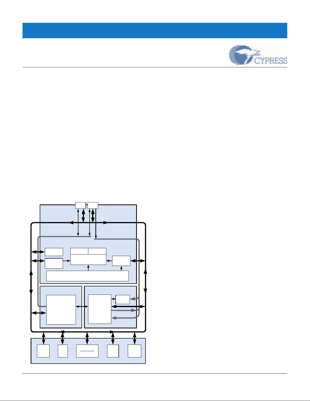
Po rt 1 Po rt 0
PSoC
CORE
System Bus
Global Digital Interconnect
SRAM
Interrupt
Controller
SROM Flash
(Includes IMO and ILO)
DIGITAL SYSTEM
Digital
PSoC Block
Array
Cloc k Sources
Global Analog Interconnect
CPU Core
(M8C)
ANALOG SYST EM
Analog
PSoC Block
Array
■ Flexible On-Chip Memory
❐ 4K Flash Program Storage 50,000 Erase/Write
Cycles
❐ 256 Bytes SRAM Data Storage
❐ In-System Serial Prog ramming (ISSP™)
❐ Partial Flash Updates
❐ Flexible Protection Mode s
❐ EEPROM Emulation in Flash
■ Complete Development Tools
❐ Free Development Software
(PSoC™ Designer)
❐ Full-Featured, In-C ircui t Emul a tor and
Programmer
❐ Full Speed Emulation
❐ Complex Breakpoint Structure
❐ 128 Bytes Trace Memory
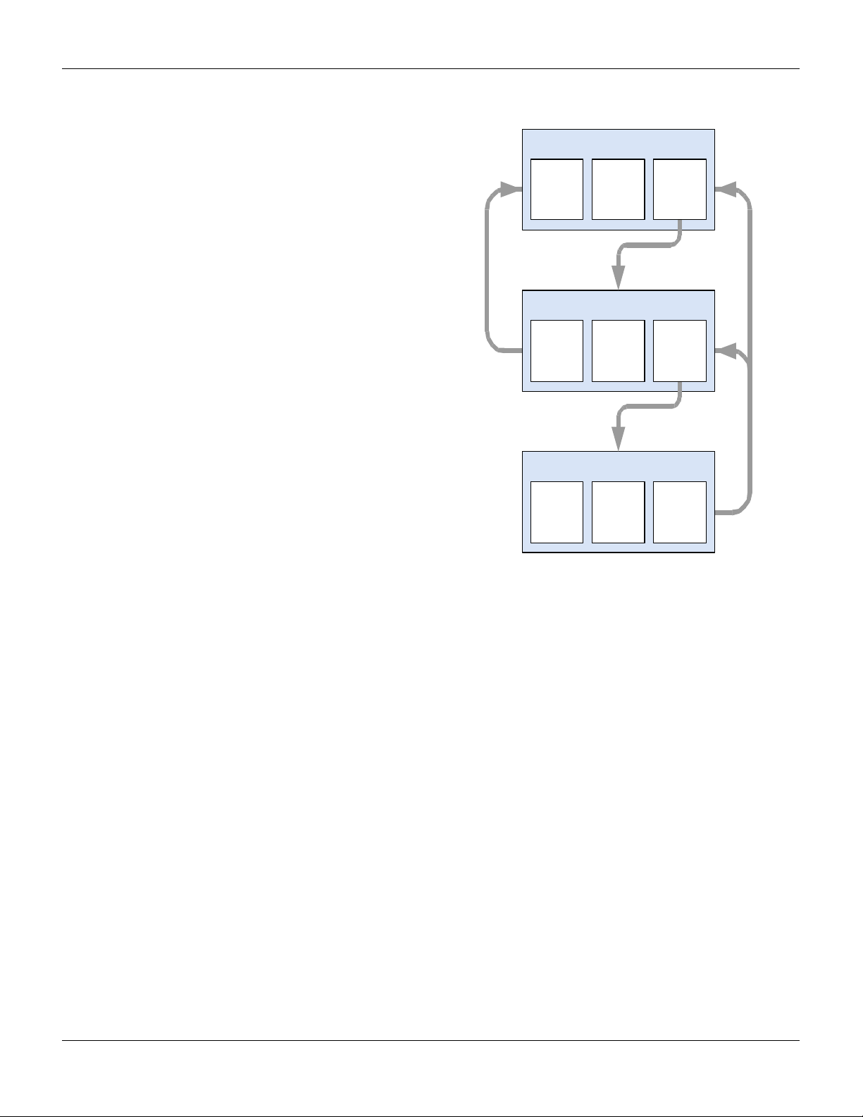
PSoC™ Functional Overview
The PSoC™ family consists of many Mixed-Signal Array with
On-Chip Controller devices. These devices are designed to
replace multiple traditional MCU-based system components
with one, low cost single-chip programmable component. A
PSoC device includes configurable blocks of analog and digital
logic, as well as programmable interconnect. This architecture
allows the user to create customized peripheral configurations,
to match the requirements of each individual application. Addi-
Sleep and
Watchdog
Analog
Ref .
tionally, a fast CPU, Flash program memory, SRAM data memory, and configurable IO are included in a range of convenient
pinouts.
The PSoC architecture, as illustrat ed on th e l ef t , is com pri se d of
four main areas: the Core, the System Resources, the Digital
System, and the Analog System. Configurable global bus
resources allow all the device resources to be combined into a
complete custom system. Each PSoC device includes four digital blocks. Depending on the PSoC package, up to two analog
comparators and up to 16 general purpose IO (GPIO) are also
included. The GPIO provide access to the global digital and
analog interconnects.
■ Precision, Programm ab le Cloc kin g
❐ Internal ±2.5% 24/48 MHz Oscillator
❐ Internal Oscillator for Watchdog and Sleep
■ Programmable Pin Configurations
❐ 25 mA Drive on All GPIO
❐ Pull Up, Pull Down, High Z, Strong, or Open
Drain Drive Modes on All GPIO
❐ Up to 8 Analog Inputs on GPIO
❐ Configurable Interrupt on All GPIO
■ Additional System Resources
2
❐ I
C™ Master, Slave and Multi-Master to
400 kHz
❐ Watchdog and Sleep Timers
❐ User-Configurable Low Voltage Detection
❐ Integrated Supervisory Circuit
❐ On-Chip Precision Voltage Reference
The PSoC Core
The PSoC Core is a powerful engine that supports a rich
instruction set. It encompasses SRAM for data storage, an
interrupt controller, sleep and watchdog timers, and IMO (internal main oscillator) and ILO (internal low speed oscillator). The
Digital
Clocks
I2C
POR and LVD
System Resets
Switch
Mode
Pump
Internal
Voltage
Ref .
SYSTEM R ESOUR CES
February 25, 2005 © Cypress Semiconductor Corp. 2004-2005 — Document No. 38-12022 Rev. *G 1
Page 2
CY8C21x23 Final Data Sheet PSoC™ Overview
CPU core, called the M8C, is a powerful processor with speeds
up to 24 MHz. The M8C is a four MIPS 8-bit Harvard architecture microp rocessor.
System Resources prov ide additional capability, such as digital
clocks to increase the flexibility of the PSoC mixed-signal
arrays, I2C functionality for implementing an I2C master, slave,
MultiMaster, an internal voltage reference that provides an
absolute value of 1.3V to a number of PSoC subsystems, a
switch mode pump (SMP) that generates normal operating voltages off a single battery cell, and various system resets supported by the M8C.
The Digital System is composed of an array of digital PSoC
blocks, which can be configured into any number of digital
peripherals. The digi tal blocks can be connected to the GPIO
through a series of global busses that can route any signal to
any pin. Freeing designs from the constraints of a fixed peripheral controller.
The Analog System is composed of four analog PSoC blocks,
supporting comparators and analog-to-digital conversion up to
8 bits in precision.
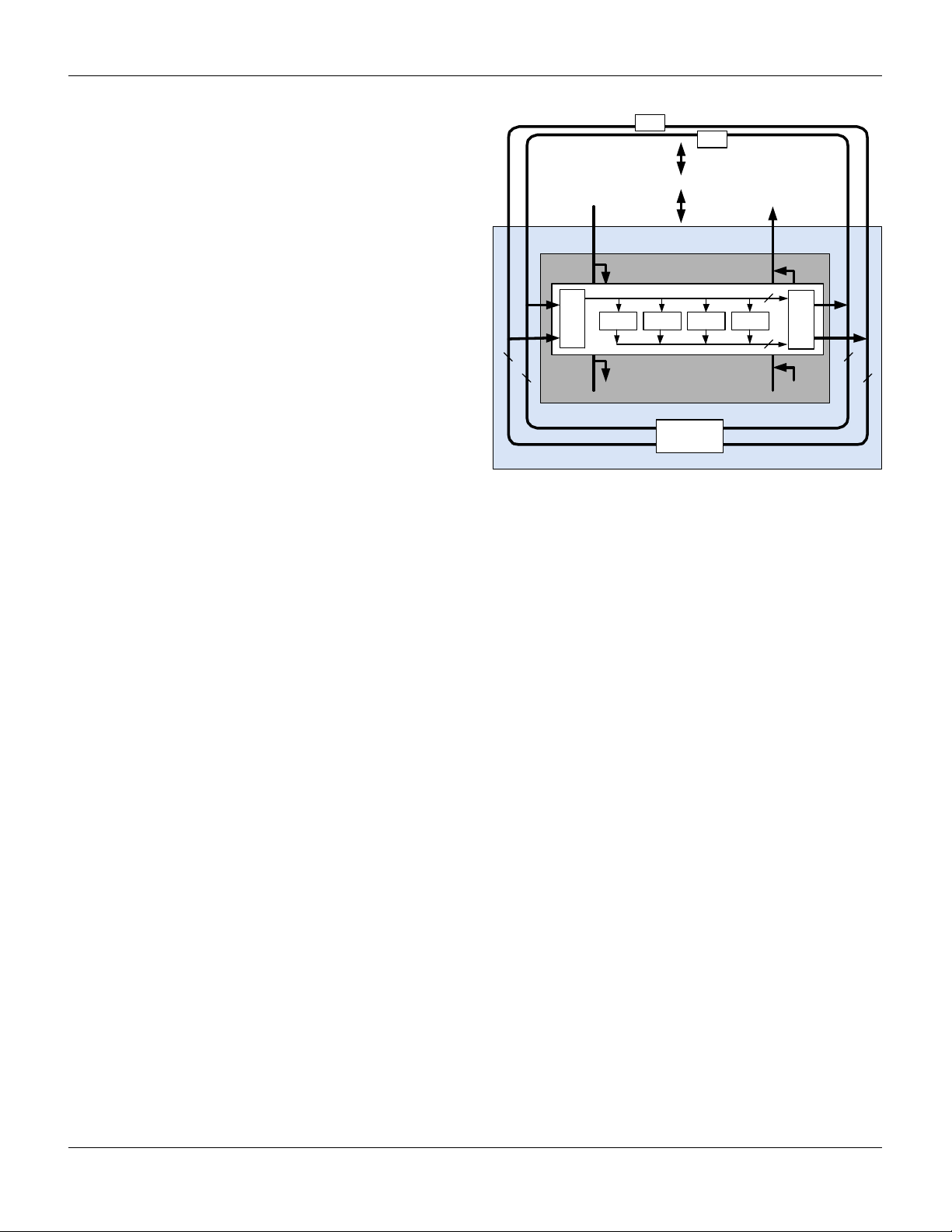
The Digital System
The Digital System is composed of 4 digital PSoC bloc ks. Each
block is an 8-bit resource that can be used alone or combined
with other blocks to fo rm 8, 16 , 24, and 32-bit p eriphe rals, wh ich
are called user module references. Digital peripheral configurations include those listed below.
■ PWMs (8 to 32 bit)
■ PWMs with Dead band (8 to 32 bit)
■ Counters (8 to 32 bit)
■ Timers (8 to 32 bit)
■ UART 8 bit with selectable parity (up to 4)
■ SPI master and slave
■ I2C slave, master, multi-master (1 availab le as a System
Resource)
■ Cyclical Redundancy Checker/Generator (8 to 32 bit)
■ IrDA (up to 4)
■ Pseudo Random Sequence Generators (8 to 32 bit)
The digital blocks can be connected to any GPIO through a
series of global bu ss es tha t c an rou t e any s ign al to any p in. The
busses also allow for signal multiplexing and for performing
logic operations. This config urabil ity frees your d esigns fro m the
constraints of a fixed peripheral controller.
Port 1
Port 0
o
c
k
o
r
e
To System Bus
s
To Analog
System
g
t
i
D
i
a
l
C
l
F
r
o
m
C
DIGITAL SYSTEM
Digital PSoC Block Array
Configuration
Row 0
DBB00 DBB01 DCB02 DCB03
Row Input
8
Configuration
GIE[7:0]
GIO[7:0]
Global Digital
Interconnect
GOE[7:0]
GOO[7:0]
Row Ou t put
4
4
8
Digital System Block Diagram
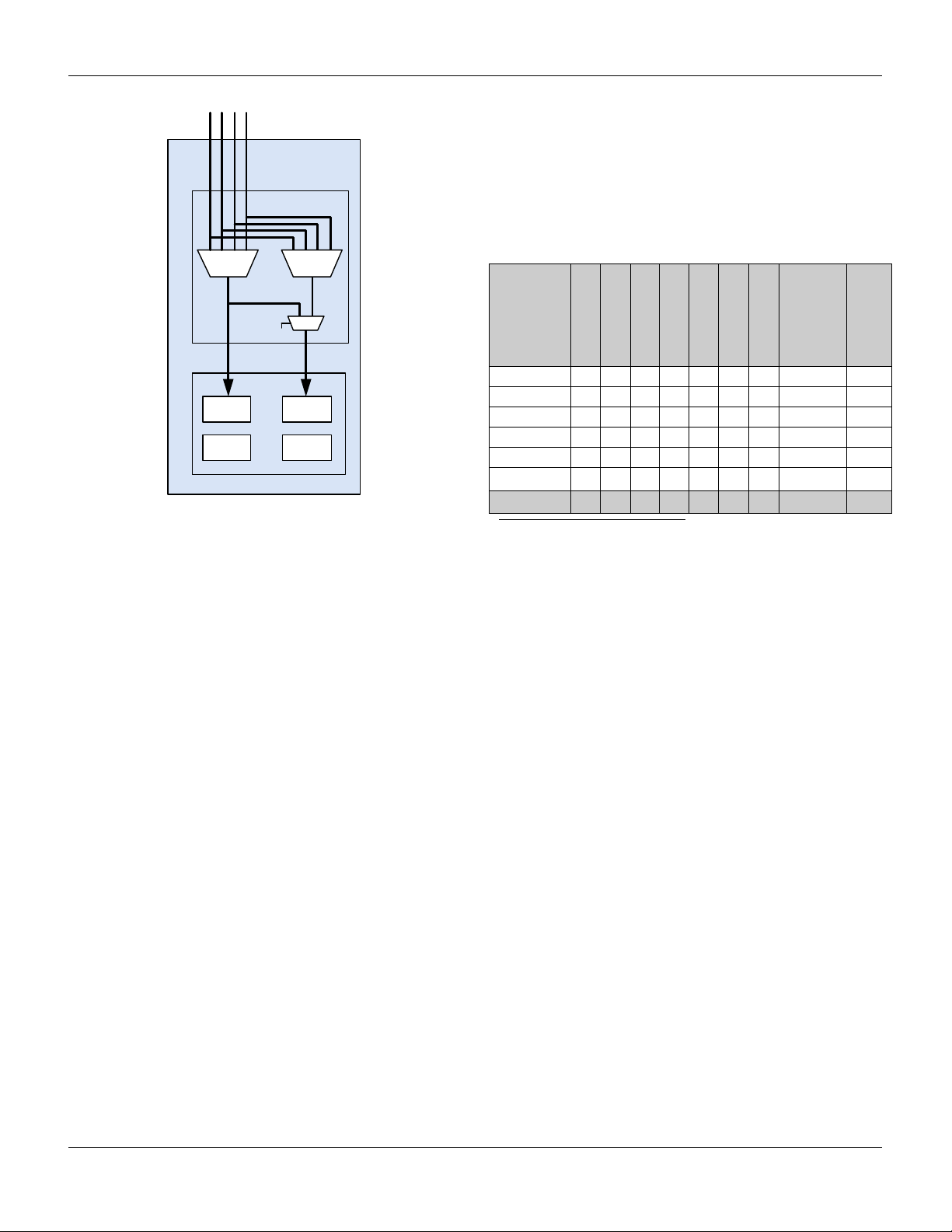
The Analog System
The Analog System is composed of 4 configurable blocks to
allow creation of complex analog signal flows. Analog peripherals are very flexible and can be customized to support specific
application requirements. Some of the more common PSoC
analog functions (most available as user modules) are listed
below.
■ Analog-to-digital converters (single or dual, with 8-bit resolu-
tion)
■ Pin-to-pin comparato r s (1)
■ Single-ended comparators (up to 2) with absolute (1.3V) ref-
erence or 8-bit DAC reference
■ 1.3V refer ence (as a System Resource)
In most PSoC devices, analog blocks are provided in columns
of three, which includes one CT (Continuous Time) and two SC
(Switched Capacitor) blocks. The CY8C21x23 devices provide
limited functionality Type “E” analog blocks. Each column contains one CT block and one SC block.
The number of blocks is on the device family which is detailed
in the table titled “PSoC Device Chara cte ris t ic s” on p age 3.
88
Digital blocks are provided in rows of four, where the number of
blocks varies by PSoC device family. This allows you the optimum choice of system resources for your application. Family
resources are shown in the table titled “PSoC Device Char ac-
teristics” on page3.
February 25, 2005 Document No. 38-12022 Rev. *G 2
Page 3
CY8C21x23 Final Data Sheet PSoC™ Overview
PSoC Device Characteristics
Array Input
Configuration
ACI0[1:0] ACI1[1:0]
ACOL1MUX
Array
ACE00 ACE01
ASE10 ASE11
Analog System Block Diagram, CY8C21x23
Additional System Resources
Depending on your PSoC device characteristics, the digital and
analog systems can have 16, 8, or 4 digital blocks and 12, 6, or
4 analog blocks. The following table lists the resources
available for specific PSoC device groups. The PSoC device
covered by this data sheet is highlighted below.
PSoC Device Characteristics
PSoC Device
Group
Digital Rows
Digital Blocks
Digital IO (Max)
CY8C29x66 64 4 16 12 4 4 12 2K 32K
CY8C27x43 44 2 8 12 4 4 12 256 Bytes 16K
CY8C24794 56 1 4 48 2 2 6 1K 16K
CY8C24x23A 24 1 4 12 2 2 6 256 Bytes 4K
CY8C24x23 24 1 4 12 2 2 6 256 Bytes 4K
CY8C21x34 28 1 4 28 0 2
CY8C21x23 16 1 4 8 0 2
a. Limited analog functionality.
Analog Inputs
Analog Outputs
Analog Blocks
Analog Columns
a
4
a
4
Amount of SRAM
512 Bytes 8K
256 Bytes 4K
Amount of Flash
System Resources, some of which have been previously listed,
provide addi tional capab ility useful to complete sy stems. Additional resources include a switch mode pump, low voltage
detection, and power on reset. Brief statements describing the
merits of each system resource are presented below.
■ Digital clock dividers provide three customizable clock fre-
quencies for use in applic ations . The clo cks can be routed to
both the digital a nd analog s ystems. Add itional c locks c an be
generated using digital PSoC blocks as clock dividers.
■ The I2C module provides 100 and 400 kHz communication
over two wires. Slave, master, and multi-master modes are
all supported.
■ Low Voltage Detection (LVD) interrupts can signal the appli-
cation of falling voltage levels, while the advanced POR
(Power On Reset) circuit eliminates the need for a system
supervisor.
■ An internal 1.3 voltage reference provides an absolute refer-
ence for the analog system, including ADCs and DACs.
■ An integrated switch mode pump (SMP) generates normal
operating voltages fr om a single 1.2 V battery cell, pro viding a
low cost boost converter.
February 25, 2005 Document No. 38-12022 Rev. *G 3
Page 4
CY8C21x23 Final Data Sheet PSoC™ Overview
Getting Started
The quickest path to understanding the PSoC silicon is by reading this data sheet and using the PSoC Designer Integrated
Development Environment (IDE). This data sheet is an overview of the PSoC integrated circuit and presents specific pin,
register, and electrical specifications. For in-depth information,
along with detailed programming information, reference the
PSoC Mixed- Signal Array Technical Referenc e Manual, which
can be found on http://www.cypress.com/psoc.
For up-to-date Ordering, Packag ing, an d Electri cal Specification
information, reference the latest PSoC device data sheets on
the web at http://www.cypress.com.
Development Kits
Development Kits are available from the following distributors:
Digi-Key, Avnet, Arrow, and Future. The Cypress Online Store
contains development kits, C compilers, and all accessories for
PSoC development. Go to the Cypres s On lin e Store web site at
http://www.cypress.com, click the Online Store shopping cart
icon at the bottom of the web page, and click PSoC (Program-
mable System-on-Chip) to view a current list of available items.
Technical Training
Free PSoC technical training is available for beginners and is
taught by a marketing or application engineer over the phone.
PSoC training classes cover designing, debugging, advanced
analog, as well as applica tion-specific classes covering topics
such as PSoC and the LIN bus. Go to http://www.cypress.com,
click on Design Support located on the left side of the web
page, and select Technical Training for more details.
Consultants
Certified PSoC Consultants offer everything from technical
assistance to complete d PSoC d esign s. To contact or become a
PSoC Consultant go to http://www.cypress.com, click on Design
Support located on the left side of the web page, and select
CYPros Consultants.
Development Tools
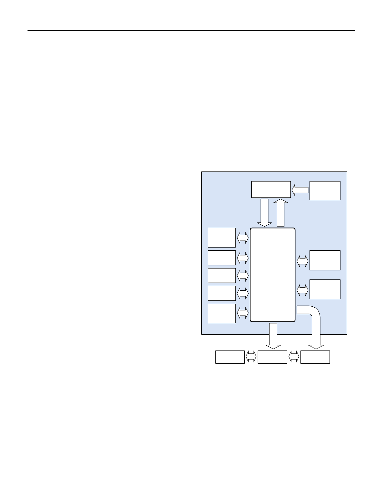
PSoC Designer is a Microsoft® Windows-based, integrated
development environment for the Programmable System-onChip (PSoC) devices. The PSoC Designer IDE and application
runs on Windows NT 4.0, Windows 2000, Windows Millennium
(Me), or Windows XP. (Reference the PSoC Designer Functional Flow diagram below.)
PSoC Designer helps the customer to select an operating configuration for the PSoC, write application code that uses the
PSoC, and debug the application. This system provides design
database management by project, an integrated debugger with
In-Circuit Emulator, in-system programming support, and the
CYASM macro assembler for the CPUs.
PSoC Designer also supports a high-level C language compiler
developed specifically for the devices in the family.
TM
PSoC
Designer
Importable
Design
Database
Dev ice
Database
Application
Database
Project
Database
User
Modules
Library
Graphical Designer
Interf ace
Results
Commands
TM
PSoC
Designer
Core
Engine
Context
Sensitive
Help
PSoC
Configuration
Sheet
Manufacturing
Information
File
Technical Support
PSoC application engineers take pride in fast and accurate
response. They can be reached with a 4-hour guaranteed
response at http://www.cypress.com/support/login.cfm.
Application Notes
Emulation
Pod
In-Circuit
Emulator
PSoC Designer Subsystems
A long list of application notes will assist you in every aspect of
your design effort. To view the PSoC application notes, go to
the http://www.cypress.com web site and select Application
Notes under the Design Resources list located in the center of
the web page. Application notes are sorted by date by default.
February 25, 2005 Document No. 38-12022 Rev. *G 4
Device
Programmer
Page 5

CY8C21x23 Final Data Sheet PSoC™ Overview
PSoC Designer Software Subsystems
Device Editor
The device editor subsystem allows the user to select different
onboard analog and digital components called user modules
using the PSoC blocks. Examples of user modules are ADCs,
DACs, Amplifiers, and Filters.
The device editor also supports easy development of multiple
configurations and dynamic reconfiguration. Dynamic reconfiguration allows for changing configurations at run time.
PSoC Designer sets up power-on initialization tables for
selected PSoC block configurations and creates source code
for an application framework. The framework contains software
to operate the selected components and, if the project uses
more than one operating configuration, contains routines to
switch between different sets of PSoC block configurations at
run time. PSoC Designer can print out a configuration sheet for
a given project configuration for use during application programming in conj unc tion with the D evice Data S heet . Once the
framework is generated, the user can add application-specific
code to flesh out the fr am ew ork . It’s also possible to change the
selected components and regenerate the framewor k.
Design Browser
The Design Browser allows users to select and import preconfigured desi g ns into th e u se r’s project. U se rs ca n ea s il y bro w se
a catalog of prec onfigured designs to facilitate time-to-design.
Examples provided in the tool s i nclude a 300-baud modem, LIN
Bus master and slave, fan controller, and magnetic card reader.
Application Editor
Debugger
The PSoC Designer Debugger subsystem provides hardware
in-circuit emulation, allowing the designer to test the program in
a physical system while providing an internal view of the PSoC
device. Debugger commands allow the designer to read the
program and read and write data memory, read and write IO
registers, read and write CPU registers, set and clear breakpoints, and provide program run, halt, and step control. The
debugger also allows the designer to create a trace buffer of
registers and memory locations of interest.
Online Help System
The online help system displays online, context-sensitive help
for the user. Designed for procedural and quick reference, each
functional subsystem has its own context-sensitive help. This
system also provides tutorials and links to FAQs and an Online
Support Forum to aid the designer in getting started.
Hardware Tools
In-Circuit Emulator
A low cost, high functionality ICE (In-Circuit Emulator) is available for development support. This hardware has the capability
to program single devices.
The emulator consists of a base unit that connects to the PC by
way of the parallel or USB port. The base unit is universal and
will operate with all PSoC devices. Emulation pods for each
device family are available separately. The emulation pod takes
the place of the PSoC device in the target board and performs
full speed (24 MHz) operation
In the Application Editor you can edit your C language and
Assembly language source code. You can also assemble, compile, link, and build.
Assembler. The macro assembler allows the assembly code
to be merged seam lessly with C code. The link libraries automatically use abso lut e addre ssing or ca n be co mpil ed in relat ive
mode, and linked with other software modules to get absolute
addressing.
C Language Compiler. A C language compiler is available
that supports PSoC family devices. Even if you have never
worked in the C langu age bef ore, the p rod uct qui ckly allows you
to create complete C programs for the PSoC family devices.
The embedded, optimizing C compiler provides all the features
of C tailored to the PSoC architecture. It comes complete with
embedded libraries providing port and bus operations, standard
keypad and display support, and extended math functionality.
February 25, 2005 Document No. 38-12022 Rev. *G 5
Page 6
CY8C21x23 Final Data Sheet PSoC™ Overview
Designing with User Modules
The development process for the PSoC device differs from that
of a traditional fixed function microprocessor. The configurable
analog and d igital hard ware blocks give the PS oC archite cture
a unique flexibility that p ays d ivide nds in mana gi ng specifi catio n
change during development and by lowering inventory costs.
These configurable resources, called PSoC Blocks, have the
ability to implement a wide variety of user-selectable functions.
Each block has several registers that de termine its function and
connectivity to other blocks, multiplexers, busses and to the IO
pins. Iterative devel op men t cy cl es perm it y ou to adapt the hardware as well as the software. This substantially lowers the risk
of having to select a different part to meet the final design
requirements.
To speed the development process, the PSoC Designer Integrated Development Environment (IDE) provides a library of
pre-built, pre-tested hardware peripheral functions, called “User
Modules.” User modules make selecting and implementing
peripheral devices simple, and come in analog, digital, and
mixed signal varieties. The standard User Module library contains over 50 common peripherals such as ADCs, DACs Timers, Counters, UARTs, and other not-so common peripherals
such as DTMF Generators and Bi-Quad analog filter sections.
Each user module establishes the basic register settings that
implement the selected function. It also provides parameters
that allow you to tailor its precise configuration to your particular
applicati on. For exam ple, a Pulse Width Modula tor User Module configures one or more digital PSoC blocks, one for each 8
bits of resolution. The user module parameters permit you to
establish the pulse width and duty cycle. User modules also
provide tested software to cut your development time. The user
module application programm ing interface (API) provides highlevel functions to co ntrol and respond to hardware events at ru n
time. The API also provides optional interrupt service routines
that you can adapt as needed.
The API functions are documented in user module data sheets
that are viewed directly in the PSo C Desi gn er ID E. Th es e data
sheets explain the internal operation of the user module and
provide performance specifications. Each data sheet describes
the use of each user mod ule p ara me ter a nd d oc um ent s the setting of each register controlled by the user module.
The development process starts when you open a new project
and bring up the Device Editor, a graphical user interface (GUI)
for configuring the hardware. You pick the user modules you
need for your project and map them onto the PSoC blocks with
point-and-click simplicity. Next, you build signal chains by interconnecting user modules to each other and the IO pins. At this
stage, you also configure the clock source connections and
enter parameter values directly or by selecting values from
drop-down menus. When you are ready to test the hardware
configuration or move on to develo ping co de for the proj ect, yo u
perform the “Generate Application” step. This causes PSoC
Designer to generate source code that automatically configures
the device to your specif ic atio n an d pro vi des the high -le vel us er
module API functions.
Devic e Ed itor
User
M odule
Selection
Placement
and
Parameter
-ization
Source
Code
Generat or
Generate
Application
Application Editor
Project
M anage r
Source
Code
Editor
Build
M ana ger
Build
All
Debugger
Interface
to ICE
Storage
Inspector
Event &
Breakpoint
M ana ger
User Module and Source Code Development Flows
The next step is to write your main program, and any sub-routines using PSoC Designer’s Application Editor subsystem.
The Application Editor includes a Project Manager that allows
you to open the project source code files (inc luding all generated code files) from a hierarchal view. The source code editor
provides syntax coloring and advanced edit features for both C
and assembly language. File search capabilities include simple
string searches and recursive “grep-style” patterns. A single
mouse click invokes the Build Manager. It employs a professional-strength “makefile” system to automatically analyze all
file dependencies and run the compiler and assembler as necessary. Project-level options control optimization strategies
used by the compiler and linker. Syntax errors are displayed in
a console window. Double clicking the error message takes you
directly to the offending line of source code. When all is correct,
the linker builds a HEX file image suitable for programming .
The last step in the devel opm en t proc es s t ak es pla ce insi de the
PSoC Designer’s Debugger subsystem. The Debugger downloads the HEX image to the In-Circuit Emulator (ICE) where it
runs at full speed. Debugger capabilities rival those of systems
costing many times more. In addition to traditional single-step,
run-to-breakpoint and watch-variable features, the Debugger
provides a large trace buffer and allows you define complex
breakpoint event s tha t inc lu de m oni tori ng ad dres s and da t a bu s
values, memory locations and external signals.
February 25, 2005 Document No. 38-12022 Rev. *G 6
Page 7
CY8C21x23 Final Data Sheet PSoC™ Overview
Document Conventions
Acronyms Used
The following table lists the acronyms that are used in this document.
Acronym Description
AC alternating current
ADC analog-to-digital converter
API application programming interface
CPU central processing unit
CT continuous time
DAC digital-to-analog converter
DC direct current
EEPROM electrically erasable programmable read-only memory
FSR full scale range
GPIO general purpose IO
IO input/output
IPOR imprecise power on reset
LSb least-significant bit
LVD low voltage detect
MSb most-significant bit
PC program counter
POR power on reset
PPOR precision power on reset
PSoC™ Programmable System-on-Chip
PWM pulse width modulator
ROM read only memory
SC switched capacitor
SMP switch mode pump
SRAM static random access memory
Units of Measure
A units of measure table is located in the Electrical Specifications section. Table 3-1 on page 14 lists all the abbreviations
used to measure the PSoC devices.
Table of Cont ents
For an in depth discussion and more information on your PSoC
device, obtain the PSoC Mixed-Signal Array Technical Refer-
ence Manual on http://www.cypress.com. This data sheet
encompasses and is organized into the following chapters and
sections.
1. Pin Information .............................. ..... ...... ..... ............... 8
1.1 Pinouts ................................................................... 8
1.1.1 8-Pin Part Pinout ...................................... 8
1.1.2 16-Pin Part Pinout ..................................... 8
1.1.3 20-Pin Part Pinout .................................... 9
1.1.4 24-Pin Part Pinout ................................. 10
2. Register Reference ..................................................... 11
2.1 Register Conventions ........................................... 11
2.2 Register Mapping Tables ..................................... 11
3. Electrical Specifications ............................................14
3.1 Absolute Maximum Ratings ................................ 15
3.2 Operating Temperature ....................................... 15
3.3 DC Electrical Characteristics ................................15
3.3.1 DC Chip-Level Specifications ................... 15
3.3.2 DC General Purpose IO Specifications .... 16
3.3.3 DC Amplifier Specifications .....................17
3.3.4 DC Switch Mode Pump Specifications ..... 18
3.3.5 DC POR and LVD Specifications ............. 19
3.3.6 DC Programming Specifications ...............20
3.4 AC Electrical Characteristics ................................ 21
3.4.1 AC Chip-Level Specifications ...................21
3.4.2 AC General Purpose IO Specifications .... 23
3.4.3 AC Amplifier Specifications ...................... 24
3.4.4 AC Digital Block Specifications .................24
3.4.5 AC External Clock Specifications .............26
3.4.6 AC Programming Specifications ............... 27
3.4.7 AC I2C Specifications ............................... 27
4. Packaging Information ............................................... 29
4.1 Packaging Dimensions .........................................29
4.2 Thermal Impedances .......................................... 31
4.3 Solder Reflow Peak Temperature ........................ 31
Numeric Naming
Hexidecimal numbers are represented with all letters in uppercase with an appended lowercase ‘h’ (for example, ‘14h’ or
‘3Ah’). Hexi d ec im al nu mber s ma y al so be re p res en t ed by a ‘0x’
prefix, the C coding convention. Binary numbers have an
5.1 Ordering Code Definitions ................................... 32
6. Sales and Service Information ..................................33
6.1 Revision History .................................................. 33
6.2 Copyrights and Flash Code Protection ................ 33
appended lowercase ‘b’ (e.g., 01010100b’ or ‘01000011b’).
Numbers not indicated by an ‘h’, ‘b’, or 0x are decimal.
February 25, 2005 Document No. 38-12022 Rev. *G 7
5. Ordering Information ..................................................32
Page 8
1. Pin Information
This chapter describes, lists, and illustrates the CY8C21x23 PSoC device pins and pinout configurations.
1.1 Pinouts
The CY8C21x23 PSoC device is available in a variety of packages which are listed and illustrated in the following tables. Every port
pin (labeled with a “P”) is capable of Digital IO. However, Vss, Vdd, SMP, and XRES are not capable of Digital IO.
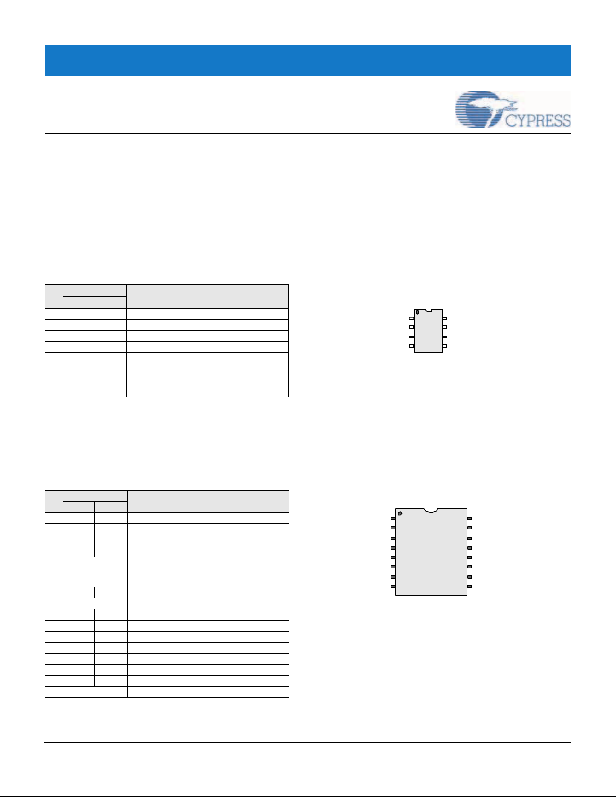
1.1.1 8-Pin Part Pinout
Table 1-1. 8-Pin Part Pinout (SOIC)
Pin
No.
1 IO I P0[5] Analog column mux input.
2 IO I P0[3] Analog column mux input.
3 IO P1[1] I2C Serial Clock (SCL), ISSP-SCLK.
4 Power Vss Ground connection.
5 IO P1[0] I2C Serial Data (SDA), ISSP-SDATA.
6 IO I P0[2] Analog column mux input.
7 IO I P0[4] Analog column mux input.
8 Power Vdd Supply voltage.
Type
Digital Analog
Pin
Name
Description
CY8C21123 8-Pin PSoC Device
1
8
A, I, P0[5]
A, I, P0[3]
I2C SCL, P1[1]
Vss
2
SOIC
3
4
Vdd
P0[4], A, I
7
P0[2], A, I
6
5
P1[0], I2C SDA
LEGEND: A = Analog, I = Input, and O = Output.
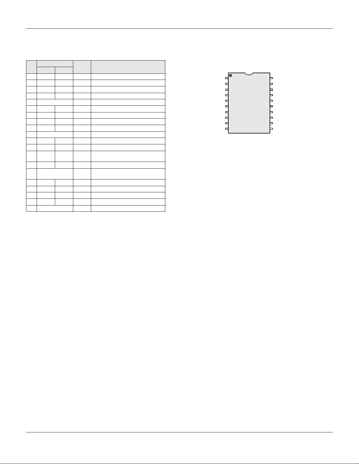
1.1.2 16-Pin Part Pinout
Table 1-2. 16-Pin Part Pinout (SOIC)
Pin
No.
1 IO I P0[7] Analog column mux input.
2 IO I P0[5] Analog column mux input.
3 IO I P0[3] Analog column mux input.
4 IO I P0[1] Analog column mux input.
5 Power SMP Switch Mode Pump (SMP) connection to
6 Power Vss Ground connection.
7 IO P1[1] I2C Serial Clock (SCL), ISSP-SCLK.
8 Power Vss Ground connection.
9 IO P1[0] I2C Serial Data (SDA), ISSP-SDATA.
10 IO P1[2]
11 IO P1[4] Optional External Clock Input (EXTCLK).
12 IO I P0[0] Analog column mux input.
13 IO I P0[2] Analog column mux input.
14 IO I P0[4] Analog column mux input.
15 IO I P0[6] Analog column mux input.
16 Power Vdd Supply voltage.
LEGEND A = Analog, I = Input, and O = Output.
Type
Digital Analog
Name Description
required external components.
CY8C21223 16-Pin PSoC Device
A, I, P0[7]
A, I, P0[5]
A, I, P0[3]
A, I, P0[1]
SMP
Vss
I2C SCL, P1[1]
Vss
1
2
3
4
5
6
7
8
SOIC
16
15
14
13
12
11
10
9
Vdd
P0[6], A, I
P0[4], A, I
P0[2], A, I
P0[0], A, I
P1[4], EXTCLK
P1[2]
P1[0], I2C SDA
February 25, 2005 Document No. 38-12022 Rev. *G 8
Page 9
CY8C21x23 Final Data Sheet 1. Pin Information
1.1.3 20-Pin Part Pinout
Table 1-3. 20-Pin Part Pinout (SSOP)
Pin
No.
1 IO I P0[7] Analog column mux input.
2 IO I P0[5] Analog column mux input.
3 IO I P0[3] Analog column mux input.
4 IO I P0[1] Analog column mux input.
5 Power Vss Ground connection.
6 IO P1[7] I2C Serial Clock (SCL).
7 IO P1[5] I2C Serial Data (SDA).
8 IO P1[3]
9 IO P1[1] I2C Serial Clock (SCL), ISSP-SCLK.
10 Power Vss Ground connection.
11 IO P1[0] I2C Serial Data (SDA), ISSP-SDATA.
12 IO P1[2]
13 IO P1[4] Optional External Clock Input (EXT-
14 IO P1[6]
15 Input XRES Active high external reset with internal
16 IO I P0[0] Analog column mux input.
17 IO I P0[2] Analog column mux input.
18 IO I P0[4] Analog column mux input.
19 IO I P0[6] Analog column mux input.
20 Power Vdd Supply voltage.
LEGEND A = Analog, I = Input, and O = Output.
Type
Digital Analog
Name Description
CLK).
pull down.
CY8C21323 20-Pin PSoC Device
A, I, P0[7 ]
A, I, P0[5]
A, I, P0[3]
A, I, P0[1]
Vss
I2C SCL, P1[7]
I2C SDA, P1[5 ]
P1[3]
I2C SCL, P1[1]
Vss
10
1
2
3
4
5
6
7
8
9
SSOP
20
19
18
17
16
15
14
13
12
11
Vdd
P0[6], A, I
P0[4], A, I
P0[2], A, I
P0[0], A, I
XRES
P1[6]
P1[4], EXTCLK
P1[2]
P1[0], I2C SDA
February 25, 2005 Document No. 38-12022 Rev. *G 9
Page 10
CY8C21x23 Final Data Sheet 1. Pin Information
I
I
I
I
I
1.1.4 24-Pin Part Pinout
Table 1-4. 24-Pin Part Pinout (MLF*)
Pin
No.
1 IO I P0[1] Analog column mux input.
2 Power SMP Switch Mode Pump (SMP) connection to
3 Power Vss Ground connection.
4 IO P1[7] I2C Serial Clock (SCL).
5 IO P1[5] I2C Se ria l Data (SDA ) .
6 IO P1[3]
7 IO P1[1] I2C Serial Clock (SCL), ISSP-SCLK.
8 NC No connection.
9 Power Vss Ground connection.
10 IO P1[0] I2C Serial Data (SDA), ISSP-SDATA.
11 IO P1[2]
12 IO P1[4] Optional External Clock Input (EXT-
13 IO P1[6]
14 Input XRES Active high external reset with internal
15 NC No connection.
16 IO I P0[0] Analog column mux input.
17 IO I P0[2] Analog column mux input.
18 IO I P0[4] Analog column mux input.
19 IO I P0[6] Analog column mux input.
20 Power Vdd Supply voltage.
21 Power Vss Ground connection.
22 IO I P0[7] Analog column mux input.
23 IO I P0[5] Analog column mux input.
24 IO I P0[3] Analog column mux input.
LEGEND A = Analog, I = Input, and O = Output.
* Note The MLF package has a center pad that must be connected to the
same ground as the Vss pin.
Type
Digital Analog
Name Description
required external compone nts.
CLK).
pull down.
CY8C21323 24-Pin PSoC Device
P0[5], A, IP0[7], A, IVss
P0[3], A,
A, I, P0 [1 ]
SMP
Vss
I2C SCL, P1[7]
I2C SDA, P1[5]
P1[3]
2423222120
1
2
MLF
3
(Top View )
4
5
6
789
NC
I2C SCL, P1[1]
101112
Vss
I2C SDA, P1[0]
P1[2]
Vdd
P0[6], A,
19
18
P0[4], A,
P0[2], A,
17
16
P0[0], A,
15
NC
14
XRE S
P1[6]
13
EXTCLK, P1[4]
February 25, 2005 Document No. 38-12022 Rev. *G 10
Page 11

2. Register Reference
This chapter lists the registers of the CY8C21x23 PSoC device. For detailed register information, reference the
PSoC™ Mixed-Signal Array Technical Reference Manual.
2.1 Register Conventions
The register conventions specific to this section are listed in the
following table.
Convention Description
R Read register or bit(s)
W Write regi ster or bit(s)
L Logical register or bit(s)
C Clearable register or bit(s)
# Access is bit specific
2.2 Register Mapping Tables
The PSoC device has a total register address space of 512
bytes. The register space is referred to as IO space and is
divided into two banks. The XOI bit in the Flag regist er (CPU_F)
determines which bank the user is currently in. When the XOI
bit is set the user is in Bank 1.
Note In the following register mapping tables, blank fields are
Reserved and should not be accessed.
February 25, 2005 Document No. 38-12022 Rev. *G 11
Page 12

CY8C21x23 Final Data Sheet 2. Register Reference
Register Map Bank 0 Table: User Space
Access
Name
PRT0DR 00 RW 40 ASE10CR0 80 RW C0
PRT0IE 01 RW 41 81 C1
PRT0GS 02 RW 42 82 C2
PRT0DM2 03 RW 43 83 C3
PRT1DR 04 RW 44 ASE11CR0 84 RW C4
PRT1IE 05 RW 45 85 C5
PRT1GS 06 RW 46 86 C6
PRT1DM2 07 RW 47 87 C7
DBB00DR0 20 # AMX_IN 60 RW A0 INT_MSK0 E0 RW
DBB00DR1 21 W 61 A1 INT_MSK1 E1 RW
DBB00DR2 22 RW PWM_CR 62 RW A2 INT_VC E2 RC
DBB00CR0 23 # 63 A3 RES_WDT E3 W
DBB01DR0 24 # CMP_CR0 64 # A4 E4
DBB01DR1 25 W 65 A5 E5
DBB01DR2 26 RW CMP_CR1 66 RW A6 DEC_CR0 E6 RW
DBB01CR0 27 # 67 A7 DEC_CR1 E7 RW
DCB02DR0 28 # ADC0_CR 68 # A8 E8
DCB02DR1 29 W ADC1_CR 69 # A9 E9
DCB02DR2 2A RW 6A AA EA
DCB02CR0 2B # 6B AB EB
DCB03DR0 2C # TMP_DR0 6C RW AC EC
DCB03DR1 2D W TMP_DR1 6D RW AD ED
DCB03DR2 2E RW TMP_DR2 6E RW AE EE
DCB03CR0 2F # TMP_DR3 6F RW AF EF
Blank fields are Reserved and should not be accessed. # Access is bit specific.
(0,Hex)
Addr
08 48 88 C8
09 49 89 C9
0A 4A 8A CA
0B 4B 8B CB
0C 4C 8C CC
0D 4D 8D CD
0E 4E 8E CE
0F 4F 8F CF
10 50 90 D0
11 51 91 D1
12 52 92 D2
13 53 93 D3
14 54 94 D4
15 55 95 D5
16 56 96 I2C_CFG D6 RW
17 57 97 I2C_SCR D7 #
18 58 98 I2C_DR D8 RW
19 59 99 I2C_MSCR D9 #
1A 5A 9A INT_CLR0 DA RW
1B 5B 9B INT_CLR1 DB RW
1C 5C 9C DC
1D 5D 9D INT_CLR3 DD RW
1E 5E 9E INT_MSK3 DE RW
1F 5F 9F DF
30 70 RDI0RI B0 RW F0
31 71 RDI0SYN B1 RW F1
32 ACE00CR1 72 RW RDI0IS B2 RW F2
33 ACE00CR2 73 RW RDI0LT0 B3 RW F3
34 74 RDI0LT1 B4 RW F4
35 75 RDI0RO0 B5 RW F5
36 ACE01CR1 76 RW RDI0RO1 B6 RW F6
37 ACE01CR2 77 RW B7 CPU_F F7 RL
38 78 B8 F8
39 79 B9 F9
3A 7A BA FA
3B 7B BB FB
3C 7C BC FC
3D 7D BD FD
3E 7E BE CPU_SCR1 FE #
3F 7F BF CPU_SCR0 FF #
Name
Access
(0,Hex)
Addr
Name
Access
(0,Hex)
Addr
Name
Access
(0,Hex)
Addr
February 25, 2005 Document No. 38-12022 Rev. *G 12
Page 13

CY8C21x23 Final Data Sheet 2. Register Reference
Register Map Ba nk 1 Table: Configuration Space
Access
Name
PRT0DM0 00 RW 40 ASE10CR0 80 RW C0
PRT0DM1 01 RW 41 81 C1
PRT0IC0 02 RW 42 82 C2
PRT0IC1 03 RW 43 83 C3
PRT1DM0 04 RW 44 ASE11CR0 84 RW C4
PRT1DM1 05 RW 45 85 C5
PRT1IC0 06 RW 46 86 C6
PRT1IC1 07 RW 47 87 C7
DBB00FN 20 RW CLK_CR0 60 RW A0 OSC_CR0 E0 RW
DBB00IN 21 RW CLK_CR1 61 RW A1 OSC_CR1 E1 RW
DBB00OU 22 RW ABF_CR0 62 RW A2 OSC_CR2 E2 RW
DBB01FN 24 RW CMP_GO_EN 64 RW A4 VLT_CMP E4 R
DBB01IN 25 RW 65 A5 ADC0_TR E5 RW
DBB01OU 26 RW AMD_CR1 66 RW A6 ADC1_TR E6 RW
DCB02FN 28 RW 68 A8 IMO_TR E8 W
DCB02IN 29 RW 69 A9 ILO_TR E9 W
DCB02OU 2A RW 6A AA BDG_TR EA RW
DCB03FN 2C RW TMP_DR0 6C RW AC EC
DCB03IN 2D RW TMP_DR1 6D RW AD ED
DCB03OU 2E RW TMP_DR2 6E RW AE EE
Blank fields are Reserved and should not be accessed. # Access is bit specific.
(1,Hex)
Addr
08 48 88 C8
09 49 89 C9
0A 4A 8A CA
0B 4B 8B CB
0C 4C 8C CC
0D 4D 8D CD
0E 4E 8E CE
0F 4F 8F CF
10 50 90 GDI_O_IN D0 RW
11 51 91 GDI_E_IN D1 RW
12 52 92 GDI_O_OU D2 RW
13 53 93 GDI_E_OU D3 RW
14 54 94 D4
15 55 95 D5
16 56 96 D6
17 57 97 D7
18 58 98 D8
19 59 99 D9
1A 5A 9A DA
1B 5B 9B DB
1C 5C 9C DC
1D 5D 9D OSC_GO_EN DD RW
1E 5E 9E OSC_CR4 DE RW
1F 5F 9F OSC_CR3 DF RW
23 AMD_CR0 63 RW A3 VLT_CR E3 RW
27 ALT_CR0 67 RW A7 E7
2B CLK_CR3 6B RW AB ECO_TR EB W
2F TMP_DR3 6F RW AF EF
30 70 RDI0RI B0 RW F0
31 71 RDI0SYN B1 RW F1
32 ACE00CR1 72 RW RDI0IS B2 RW F2
33 ACE00CR2 73 RW RDI0LT0 B3 RW F3
34 74 RDI0LT1 B4 RW F4
35 75 RDI0RO0 B5 RW F5
36 ACE01CR1 76 RW RDI0RO1 B6 RW F6
37 ACE01CR2 77 RW B7 CPU_F F7 RL
38 78 B8 F8
39 79 B9 F9
3A 7A BA FLS_PR1 FA RW
3B 7B BB FB
3C 7C BC FC
3D 7D BD FD
3E 7E BE CPU_SCR1 FE #
3F 7F BF CPU_SCR0 FF #
Name
Access
(1,Hex)
Addr
Name
Access
(1,Hex)
Addr
Name
(1,Hex)
Addr
Access
February 25, 2005 Document No. 38-12022 Rev. *G 13
Page 14

3. Electrical S pecifications
This chapter presents the DC and AC electrical specifications of the CY8C21x23 PSoC device. For the most up to date electrical
specifications, confirm that you have the most recent data sheet by going to the web at http://www.cypress.com/psoc.
Specifi cations are valid for -40
Refer to Table 3-15 for the electrical specifications on the internal main oscillator (IMO) using SLIMO mode.
o
C ≤ TA ≤ 85oC and TJ ≤ 100oC, except where noted.
5.25
5.25
SLIMO
Mode=1
4.75
Vdd Volta ge
3.00
2.40
V
p
a
e
l
R
93 kHz 12 MHz 24 MHz
3 MHz
i
r
d
a
e
t
g
i
n
i
o
g
n
CPU Frequency
4.75
Vdd Voltage
3.60
3.00
2.40
93 kHz
SLIMO Mode = 0
SLIMO
Mode=1
SLIMO
Mode=1
IMO Frequency
Mode=1
6 MHz
SLIMO
12 MHz 24 MHz
O
Figure 3-1a. Voltage versus CPU Frequency Figure 3-1b. Voltage versus IMO Frequency
The following table lists the units of measure that are used in this chapter.
Table 3-1: Units of Measure
Symbol Unit of Measure Symbol Unit of Measure
o
C
dB decibels mA milli-ampere
fF femto farad ms milli-second
Hz hertz mV milli-volts
KB 1024 bytes nA nanoampere
Kbit 1024 bits ns nanosecond
kHz kilohertz nV nanovolts
kΩ kilohm Ω ohm
MHz megahertz pA picoampere
MΩ megaohm pF picofarad
µA microampere pp peak-to-peak
µF microfarad ppm parts per million
µH microhenry ps picosecond
µs microsecond sps samples per second
µV microvolts σ sigma: one standard deviation
µVrms microvolts root-mean-square V volts
degree Cels i us µW microwatts
SLIMO
Mode=0
SLIMO
Mode=0
February 2005 Document No. 38-12022 Rev. *G 14
Page 15

CY8C21x23 Final Data Sheet 3. Electrical Specifications
3.1 Absolute Maximum Ratings
Table 3-2. Absolute Maximum Ratings
Symbol Description Min Typ Max Units Notes
T
STG
T
A
Vdd Supply Voltage on Vdd Relative to Vss -0.5 – +6.0 V
V
IO
V
IOZ
I
MIO
ESD Electro Static Discharge Voltage 2000 – – V Human Body Model ESD.
LU Latch-up Current – – 200 mA
Storage Temperature -55 – +100
Ambient Temperature with Power Applied -40 – +85
DC Input Voltage Vss - 0.5 – Vdd + 0.5 V
DC Voltage Applied to Tri-st ate Vss - 0.5 – Vdd + 0.5 V
Maximum Current into any Port Pin -25 – +50 mA
o
C
o
C
Higher storage temperatures will reduce data
retention time.
3.2 Operating Temperature
Table 3-3. Operating Temperature
Symbol Description Min Typ Max Units Notes
T
A
T
J
Ambient Temperature -40 – +85
Junction Temperature -40 – +100
o
C
o
C
The temperature rise from ambient to junction is
package specific. See “Thermal Impedances”
on page 31. The user must limit the power con-
sumption to comply with this requirement.
3.3 DC Electrical Characteristics
3.3.1 DC Chip-Level Specifications
The following table lists guaranteed maximum and minimum specifications for the voltage and temperature ranges: 4.75V to 5.25V
and -40°C ≤ T
apply to 5V, 3.3V, or 2.7V at 25°C and are for design guidance only.
Ta ble 3-4. DC Chip-Level Specifications
Symbol Description Min Typ Max Units Notes
Vdd Supply Voltage 2.40 – 5.25 V See DC POR and LVD specifications, Table 3-11
I
DD
I
DD3
I
DD27
I
SB27
I
SB
V
REF
V
REF27
AGND Analog Ground V
≤ 85°C, 3.0V to 3.6V and -4 0°C ≤ TA ≤ 85°C, or 2.4V to 3.0V a nd -40°C ≤ TA ≤ 85°C, respecti vely. Typica l pa ram eters
A
on page 19.
Supply Current, IMO = 24 MHz – 3 4 mA
Supply Current, IMO = 6 MHz – 1.2 2 mA
Supply Current, IMO = 6 MHz – 1.1 1.5 mA
Sleep (Mode) Current with POR, LVD, Sleep Timer, WDT,
and internal slow oscillator active. Mid temperature range.
Sleep (Mode) Current with POR, LVD, Sleep Timer, WDT,
and internal slow oscillator active.
Reference Voltage (Bandgap) 1.28 1.30 1.32 V Trimmed for appropriate Vdd. Vdd = 3.0V to
Reference Voltage (Bandgap) 1.16 1.30 1.330 V Trimmed for appropriate Vdd. Vdd = 2.4V to
– 2.6 4 µA
– 2.8 5 µA
REF
- 0.003
V
REF
V
REF
+ 0.003
V
Conditions are Vdd = 5.0V, 25oC, CPU = 3 MHz,
SYSCLK doubler disabled. VC1 = 1.5 MHz, VC2
= 93.75 kHz, VC3 = 0.366 kHz.
Conditions are Vdd = 3.3V, 25oC, CPU = 3 MHz,
clock doubler disabled. VC1 = 375 kHz, VC2 =
23.4 kHz, VC3 = 0.091 kHz.
Conditions are Vdd = 2.55V, 25oC, CPU = 3
MHz, clock doubler disabled. VC1 = 375 kHz,
VC2 = 23.4 kHz, VC3 = 0.091 kHz.
Vdd = 2.55V, 0oC to 40oC.
Vdd = 3.3V, -40oC ≤ TA ≤ 85oC.
5.25V.
3.0V.
February 25, 2005 Document No. 38-12022 Rev. *G 15
Page 16

CY8C21x23 Final Data Sheet 3. Electrical Specifications
3.3.2 DC General Purpose IO Specifications
The following table lists guaranteed maximum and minimum specifications for the voltage and temperature ranges: 4.75V to 5.25V
and -40°C ≤ T
are for design guidance only.
Table 3-5. 5V and 3.3V DC GPIO Specifications
Symbol Description Min Typ Max Units Notes
R
PU
R
PD
V
OH
V
OL
V
IL
V
IH
V
H
I
IL
C
IN
C
OUT
≤ 85°C, 3.0V to 3.6V and -40°C ≤ TA ≤ 85°C, respectively. Typical param ete rs ap ply to 5V, 3.3V, or 2.7V at 25°C and
A
Pull up Resistor 4 5.6 8 kΩ
Pull down Resistor 4 5.6 8 kΩ
High Output Level Vdd - 1.0 – – V IOH = 10 mA, Vdd = 4.75 to 5.25V (8 total loads,
4 on even port pins (for example, P0[2], P1[4]),
4 on odd port pins (for example, P0[3], P1[5])).
80 mA maximum combined IOH budget.
Low Output Level – – 0.75 V I OL = 25 mA, V dd = 4. 75 to 5.25 V (8 to t al loa ds ,
4 on even port pins (for example, P0[2], P1[4]),
4 on odd port pins (for example, P0[3], P1[5])).
150 mA maximum combined IOL budget.
Input Low Level – – 0.8 V Vdd = 3.0 to 5.25.
Input High Level 2.1 – V Vdd = 3.0 to 5.25.
Input Hysteresis – 60 – mV
Input Leakage (Absolute Value) – 1 – nA Gross tested to 1 µA.
Capacitive Load on Pins as Input – 3.5 10 pF
Capacitive Load on Pins as Output – 3.5 10 pF
Package and pin dependent. Temp = 25oC.
Package and pin dependent. Temp = 25oC.
The following table lists guaranteed maximu m and minimum specifications for the v ol t ag e and temperature ranges: 2.4V to 3.0V and
-40°C ≤ T
≤ 85°C. Typical parameters apply to 2.7V at 25°C and are for design guidance only.
A
Table 3-6. 2.7V DC GPIO Specifications
Symbol Description Min Typ Max Units Notes
R
PU
R
PD
V
OH
V
OL
V
IL
V
IH
V
H
I
IL
C
IN
C
OUT
Pull up Resistor 4 5.6 8 kΩ
Pull down Resistor 4 5.6 8 kΩ
High Output Level Vdd - 0.4 – – V IOH = 2.5 mA (6.25 Typ), Vdd = 2.4 to 3.0V (16
mA maximum, 50 mA Typ combined IOH budget).
Low Output Level – – 0.75 V IOL = 10 mA, Vdd = 2.4 to 3.0V (90 mA maxi-
mum combined IOL budget).
Input Low Level – – 0.75 V Vdd = 2.4 to 3.0.
Input High Level 2.0 – – V Vdd = 2.4 to 3.0.
Input Hysteresis – 60 – mV
Input Leakage (Absolute Value) – 1 – nA Gross tested to 1 µA.
Capacitive Load on Pins as Input – 3.5 10 pF
Capacitive Load on Pins as Output – 3.5 10 pF
Package and pin dependent. Temp = 25oC.
Package and pin dependent. Temp = 25oC.
February 25, 2005 Document No. 38-12022 Rev. *G 16
Page 17

CY8C21x23 Final Data Sheet 3. Electrical Specifications
3.3.3 DC Amplifier Specifications
The following tables list guaranteed maximum and minimum specifications for the voltage and temperature ranges: 4.75V to 5.25V
and -40°C ≤ T
apply to 5V, 3.3V, or 2.7V at 25°C and are for design guidance only.
Table 3-7. 5V DC Amplifier Specifications
Symbol Description Min Typ Max Units Notes
V
OSOA
TCV
OSOA
I
EBOA
C
INOA
V
CMOA
≤ 85°C, 3.0V to 3.6V and -4 0°C ≤ TA ≤ 85°C, or 2.4V to 3.0V a nd -40°C ≤ TA ≤ 85°C, respecti vely. Typica l pa ram eters
A
Input Offset Voltage (absolute value) – 2.5 15 mV
Average Input Offset Voltage Drift – 10 –
µV/
o
C
Input Leakage Current (Port 0 Analog Pins) – 200 – pA Gross tested to 1 µA.
Input Capacitance (Port 0 Analog Pins) – 4.5 9.5 pF
Package and pin dependent. Temp = 25
Common Mode Voltage Range 0.0 – Vdd - 1 V
o
C.
G
I
OLOA
SOA
Open Loop Gain 80 – – dB
Amplifier Supply Current – 10 30 µA
Ta ble 3-8. 3.3V DC Amplifier Specifications
Symbol Description Min Typ Max Units Notes
V
OSOA
TCV
I
EBOA
C
INOA
V
CMOA
G
OLOA
I
SOA
OSOA
Input Offset Voltage (absolute value) – 2.5 15 mV
Average Input Offset Voltage Drift – 10 –
µV/
o
C
Input Leakage Current (Port 0 Analog Pins) – 200 – pA Gross tested to 1 µA.
Input Capacitance (Port 0 Analog Pins) – 4.5 9.5 pF
Package and pin dependent. Temp = 25
Common Mode Voltage Range 0 – Vdd - 1 V
Open Loop Gain 80 – – dB
Amplifier Supply Current – 10 30 µA
Ta ble 3-9. 2.7V DC Amplifier Specifications
Symbol Description Min Typ Max Units Notes
V
OSOA
TCV
I
EBOA
C
INOA
V
CMOA
G
OLOA
I
SOA
OSOA
Input Offset Voltage (absolute value) – 2.5 15 mV
Average Input Offset Voltage Drift – 10 –
µV/
o
C
Input Leakage Current (Port 0 Analog Pins) – 200 – pA Gross tested to 1 µA.
Input Capacitance (Port 0 Analog Pins) – 4.5 9.5 pF
Package and pin dependent. Temp = 25
Common Mode Voltage Range 0 – Vdd - 1 V
Open Loop Gain 80 – – dB
Amplifier Supply Current – 10 30 µA
o
C.
o
C.
February 25, 2005 Document No. 38-12022 Rev. *G 17
Page 18

CY8C21x23 Final Data Sheet 3. Electrical Specifications
3.3.4 DC Switch Mode Pump Specifications
The following table lists guaranteed maximum and minimum specifications for the voltage and temperature ranges: 4.75V to 5.25V
and -40°C ≤ T
apply to 5V, 3.3V, or 2.7V at 25°C and are for design guidance only.
Ta ble 3-10. DC Switch Mode Pump (SMP) Specifications
Symbol Description Min Typ Max Uni ts Notes
V
PUMP5V
V
PUMP3V
V
PUMP2V
I
PUMP
V
BAT5V
V
BAT3V
V
BAT2V
V
BATSTART
∆V
PUMP_Line
∆V
PUMP_Load
∆V
PUMP_Ripple
E
3
E
2
F
PUMP
DC
PUMP
a. L1 = 2 µH inductor, C1 = 10 µF capacitor, D1 = Schottky diode. See Figure3-2.
≤ 85°C, 3.0V to 3.6V and -4 0°C ≤ TA ≤ 85°C, or 2.4V to 3.0V a nd -40°C ≤ TA ≤ 85°C, respecti vely. Typica l pa ram eters
A
5V Output Voltage from Pump 4.75 5.0 5.25 V
Configuration of footnote.
a
Average, neglecting
ripple. SMP trip voltage is set to 5.0V.
3.3V Output Voltage from Pump 3.00 3.25 3.60 V
Configuration of footnote.
a
Average, neglecting
ripple. SMP trip voltage is set to 3.25V.
2.6V Output Voltage from Pump 2.45 2.55 2.80 V
Configuration of footnote.
a
Average, neglecting
ripple. SMP trip voltage is set to 2.55V.
Available Output Current
V
BAT
V
BAT
V
BAT
= 1.8V, V
= 1.5V, V
= 1.3V, V
PUMP
PUMP
PUMP
= 5.0V
= 3.25V
= 2.55V
5
8
8
–
–
–
–
–
–
Input Voltage Range from Battery 1.8 – 5.0 V
Input Voltage Range from Battery 1.0 – 3.3 V
mA
mA
mA
Configuration of footnote.
SMP trip voltage is set to 5.0V.
SMP trip voltage is set to 3.25V.
SMP trip voltage is set to 2.55V.
Configuration of footnote.
set to 5.0V.
Configuration of footnote.
a
a
SMP trip voltage is
a
SMP trip voltage is
set to 3.25V.
Input Voltage Range from Battery 1.0 – 2.8 V
Configuration of footnote.
a
SMP trip voltage is
set to 2.55V.
Minimum Input Voltage from Battery to Start Pump 1.2 – – V
Line Regulation (over Vi range) – 5 – % V
Configuration of footnote.
1.25V at T
Configuration of footnote.a VO is the “Vdd Value
O
for PUMP Trip” specified by the VM[2:0] setting
= -40oC.
A
a 0o
C ≤ TA ≤ 100.
in the DC POR and LVD Specification, Table 3-
11 on page19.
Load Regulation – 5 – %V
Configuration of footnote.a VO is the “Vdd Value
O
for PUMP Trip” specified by the VM[2:0] setting
in the DC POR and LVD Specification, Table 3-
11 on page19.
Output Voltage Ripple (depends on cap/load) – 100 – mVpp
Efficiency 35 50 – %
Configuration of footnote.
Configuration of footnote.
a
Load is 5 mA.
a
Load is 5 mA. SMP
trip voltage is set to 3.25V.
Efficiency 35 80 – % For I load = 1mA, V
10 uH inductor, 1 uF capacitor, and Schottky
PUMP
= 2.55V, V
BAT
= 1.3V,
diode.
Switching Frequency – 1.3 – MHz
Switching Duty Cycle – 50 – %
D1
Vdd
L
1
+
V
Battery
BAT
SMP
Vss
PSoC
TM
V
PUMP
C1
Figure 3-2. Basic Switch Mode Pump Circuit
February 25, 2005 Document No. 38-12022 Rev. *G 18
Page 19
CY8C21x23 Final Data Sheet 3. Electrical Specifications
3.3.5 DC POR and LVD Specifications
The following table lists guaranteed maximum and minimum specifications for the voltage and temperature ranges: 4.75V to 5.25V
and -40°C ≤ T
apply to 5V, 3.3V, or 2.7V at 25°C and are for design guidance only.
Table 3-11. DC POR and LVD Specifications
Symbol Description Min Typ Max Units Notes
V
PPOR0
V
PPOR1
V
PPOR2
V
LVD0
V
LVD1
V
LVD2
V
LVD3
V
LVD4
V
LVD5
V
LVD6
V
LVD7
V
PUMP0
V
PUMP1
V
PUMP2
V
PUMP3
V
PUMP4
V
PUMP5
V
PUMP6
V
PUMP7
a. Always greater than 50 mV above V
b. Always greater than 50 mV above V
c. Always greater than 50 mV above V
d. Always greater than 50 mV above
≤ 85°C, 3.0V to 3.6V and -4 0°C ≤ TA ≤ 85°C, or 2.4V to 3.0V a nd -40°C ≤ TA ≤ 85°C, respecti vely. Typica l pa ram eters
A
Vdd Value for PPOR Trip
PORLEV[1:0] = 00b
PORLEV[1:0] = 01b
PORLEV[1:0] = 10b
2.36
–
2.82
4.55
2.40
2.95
4.70
V
V
V
Vdd must be greater than or equal to 2.5V
during startup, reset from the XRES pin, or
reset from Watchdog.
Vdd Value for LVD Trip
a
VM[2:0] = 000b
VM[2:0] = 001b
VM[2:0] = 010b
VM[2:0] = 011b
VM[2:0] = 100b
VM[2:0] = 101b
VM[2:0] = 110b
VM[2:0] = 111b
2.40
2.85
2.95
3.06
4.37
4.50
4.62
4.71
2.45
2.92
3.02
3.13
4.48
4.64
4.73
4.81
2.51
2.99
3.09
3.20
4.55
4.75
4.83
4.95
V
b
V
V
V
V
V
V
V
Vdd Value for PUMP Trip
VM[2:0] = 000b
VM[2:0] = 001b
VM[2:0] = 010b
VM[2:0] = 011b
VM[2:0] = 100b
VM[2:0] = 101b
VM[2:0] = 110b
VM[2:0] = 111b
(PORLEV = 00) for falling supply.
PPOR
(PORLEV = 01) for falling supply.
PPOR
.
LVD0
V
.
LVD3
2.45
2.96
3.03
3.18
4.54
4.62
4.71
4.89
2.55
3.02
3.10
3.25
4.64
4.73
4.82
5.00
2.62
3.09
3.16
3.32
4.74
4.83
4.92
5.12
c
V
V
V
V
d
V
V
V
V
February 25, 2005 Document No. 38-12022 Rev. *G 19
Page 20

CY8C21x23 Final Data Sheet 3. Electrical Specifications
3.3.6 DC Programming Specifications
The following table lists guaranteed maximum and minimum specifications for the voltage and temperature ranges: 4.75V to 5.25V
and -40°C ≤ T
apply to 5V, 3.3V, or 2.7V at 25°C and are for design guidance only.
Ta ble 3-12. DC Programming Specifications
Symbol Description Min Typ Max Units Notes
Vdd
IWRITE
I
DDP
V
ILP
V
IHP
I
ILP
I
IHP
V
OLV
V
OHV
Flash
ENPB
Flash
ENT
Flash
DR
a. A maximum of 36 x 50,000 block endurance cycles is allowed. This may be balanced between operations on 36x1 blocks of 50,000 maximum cycles each, 36x2 blocks of
25,000 maximum cycles each, or 36x4 blocks of 12,500 maximum cycles each (and so forth to limit the total number of cycles to 36x50,000 and that no single block ever
sees more than 50,000 cycles).
For the full industrial range, the user must employ a temperature sensor user module (FlashTemp) and feed the result to the temperature argument before writing. Refer to
the Flash APIs Application Note AN2015 at http://www.cypress.com under Application Notes for more information.
≤ 85°C, 3.0V to 3.6V and -4 0°C ≤ TA ≤ 85°C, or 2.4V to 3.0V a nd -40°C ≤ TA ≤ 85°C, respecti vely. Typica l pa ram eters
A
Supply Voltage for Flash Write Operations 2.70 – – V
Supply Current During Programming or Verify – 5 25 mA
Input Low Voltage During Programming or Verify – – 0.8 V
Input High Voltage During Programming or Verify 2.2 – – V
Input Current when Applying Vilp to P1[0] or P1[1] During
Programming or Verify
Input Current when Applying Vihp to P1[0] or P1[1] During
Programming or Verify
Output Low Voltage During Programming or V erify – – Vss + 0.75 V
Output High Voltage During Programming or Verify Vdd - 1.0 – Vdd V
Flash Endurance (per block) 50,000 – – – Erase/write cycles per block.
Flash Endurance (total)
Flash Data Retention 10 – – Years
a
– – 0.2 mA Driving internal pull-down resistor.
– – 1.5 mA Driving internal pull-down resistor.
1,800,0000–
0
0
–
0
–
Erase/write cycles.
0
February 25, 2005 Document No. 38-12022 Rev. *G 20
Page 21

CY8C21x23 Final Data Sheet 3. Electrical Specifications
3.4 AC Electrical Characteristics
3.4.1 AC Chip-Level Specifications
The following table lists guaranteed maximum and minimum specifications for the voltage and temperature ranges: 4.75V to 5.25V
and -40°C ≤ T
apply to 5V, 3.3V, or 2.7V at 25°C and are for design guidance only..
Ta ble 3-13. 5V and 3.3V AC Chip-Level Specifications
Symbol Description Min Typ Max Units Notes
F
IMO24
F
IMO6
F
CPU1
F
CPU2
F
BLK5
F
BLK33
F
32K1
Jitter32k 32 kHz RMS Period Jitter – 100 200 ns
Jitter32k 32 kHz Peak-to-Peak Period Jitter – 1400 – ns
T
XRST
DC24M 24 MHz Duty Cycle 40 50 60 %
Step24M 24 MHz Trim Step Size – 50 – kHz
Fout48M 48 MHz Output Frequency 46.8 48.0
Jitter24M1 24 MHz Peak-to-Peak Period Jitter (IMO) – 300 ps
F
MAX
T
RAMP
a. 4.75V < Vdd < 5.25V.
b. Accuracy derived from Internal Main Oscillator with appropriate trim for Vdd range.
c. 3.0V < Vdd < 3.6V. See Application Note AN2012 “Adjusting PSoC Microcontroller Trims for Dual Voltage-Range Operation” for information on trimming for operation at 3.3V.
d. See the individual user module data sheets for information on maximum frequencies for user modules.
≤ 85°C, 3.0V to 3.6V and -4 0°C ≤ TA ≤ 85°C, or 2.4V to 3.0V a nd -40°C ≤ TA ≤ 85°C, respecti vely. Typica l pa ram eters
A
Internal Main Oscillator Frequency for 24 MHz 23.4 24
24.6
a,b,c
MHz Trimmed for 5V or 3.3V operation using
factory trim values. See Figure 3-1b on
page 14. SLIMO mode = 0.
Internal Main Oscillator Frequency for 6 MHz 5.75 6
6.35
a,b,c
MHz Trimmed for 3.3V operation using factory
trim values. See Figure 3-1b on page 14.
SLIMO mode = 1.
CPU Frequency (5V Nominal) 0.93 24
CPU Frequency (3.3V Nominal) 0.93 12
Digital PSoC Block Frequency0(5V Nominal)
0 48
Digital PSoC Block Frequency (3.3V Nominal) 0 24
24.6
12.3
49.2
24.6
a,b
MHz 24 MHz only for SLIMO mode = 0.
b,c
MHz
a,b,d
MHz Refer to the AC Digital Block Specifica-
tions below.
b,d
MHz
Internal Low Speed Oscillator Frequency 15 32 64 kHz
External Reset Pulse Width 10 – – µs
a,c
49.2
MHz Trimmed. Utilizing factory trim values.
Maximum frequency of signal on row input or row output. – – 12.3 MHz
Supply Ramp Time 0 – – µs
Ta ble 3-14. 2.7V AC Chip-Level Specifications
Symbol Description Min Typ Max Units Notes
F
IMO12
F
IMO6
F
CPU1
F
BLK27
F
32K1
Internal Main Oscillator Frequency for 12 MHz
11.5 12
Internal Main Oscillator Frequency for 6 MHz 5.5 6
CPU Frequency (2.7V Nominal) 0.093 3
Digital PSoC Block Frequency (2.7V Nominal) 0 12
Internal Low Speed Oscillator Frequency 8 32 96 kHz
Jitter32k 32 kHz RMS Period Jitter – 150 200 ns
Jitter32k 32 kHz Peak-to-Peak Period Jitter – 1400 – ns
T
F
T
XRST
MAX
RAMP
External Reset Pulse Width 10 – – µs
Maximum frequency of signal on row input or row output. – – 12.3 MHz
Supply Ramp Time 0 – – µs
a. 2.4V < Vdd < 3.0V.
b. Accuracy derived from Internal Main Oscillator with appropriate trim for Vdd range.
c. See Application Note AN2012 “Adjusting PSoC Microcontroller Trims for Dual Voltage-Range Operation” for information on maximum frequency for user modules.
0
12.7
6.35
3.15
12.5
a,b,c
MHz Trimmed for 2.7V operation using factory
a,b,c
MHz Trimmed for 2.7V operation using factory
a,b
MHz 24 MHz only for SLIMO mode = 0.
a,b,c
MHz Refer to the AC Digital Block Specifica-
trim values. See Figure 3-1b on page 14.
SLIMO mode = 1.
trim values. See Figure 3-1b on page 14.
SLIMO mode = 1.
tions below.
February 25, 2005 Document No. 38-12022 Rev. *G 21
Page 22
CY8C21x23 Final Data Sheet 3. Electrical Specifications
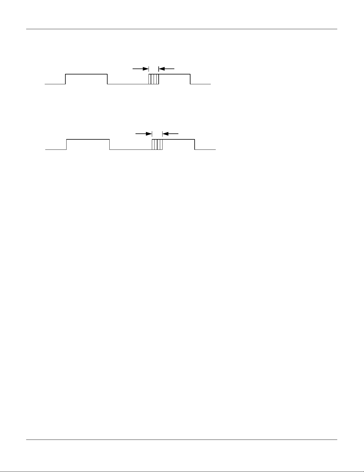
Jitter24M 1
F
24M
Figure 3-3. 24 MHz Period Jitter (IMO) Timing Diagram
Jitter32k
F
32K1
Figure 3-4. 32 kHz Period Jitter (ILO) Timing Diagram
February 25, 2005 Document No. 38-12022 Rev. *G 22
Page 23

CY8C21x23 Final Data Sheet 3. Electrical Specifications
3.4.2 AC General Purpose IO Specifications
The following table lists guaranteed maximum and minimum specifications for the voltage and temperature ranges: 4.75V to 5.25V
and -40°C ≤ T
apply to 5V, 3.3V, or 2.7V at 25°C and are for design guidance only.
Table 3-15. 5V and 3.3V AC GPIO Specifications
Symbol Description Min Typ Max Units Notes
F
GPIO
TRiseF Rise Time, Normal Strong Mode, Cload = 50 pF 3 – 18 ns Vdd = 4.5 to 5.25V, 10% - 90%
TFallF Fall Time, Normal Strong Mode, Cload = 50 pF 2 – 18 ns Vdd = 4.5 to 5.25V, 10% - 90%
TRiseS Rise Time, Slow Strong Mode, Cload = 50 pF 10 27 – ns Vdd = 3 to 5.25V, 10% - 90%
TFallS Fall Time, Slow Strong Mode, Cload = 50 pF 10 22 – ns Vdd = 3 to 5.25V, 10% - 90%
Ta ble 3-16. 2.7V AC GPIO Specifications
Symbol Description Min Typ Max Units Notes
F
GPIO
TRiseF Rise Time, Normal Strong Mode, Cload = 50 pF
TFallF Fall Time, Normal Strong Mode, Cload = 50 pF
TRiseS Rise Time, Slow Strong Mode, Cload = 50 pF
TFallS Fall Time, Slow Strong Mode, Cload = 50 pF
≤ 85°C, 3.0V to 3.6V and -4 0°C ≤ TA ≤ 85°C, or 2.4V to 3.0V a nd -40°C ≤ TA ≤ 85°C, respecti vely. Typica l pa ram eters
A
GPIO Operating Frequenc y 0 – 12 MHz Normal Strong Mode
GPIO Operating Frequenc y 0 – 3 MHz Normal Strong Mode
6 – 50 ns Vdd = 2.4 to 3.0V, 10% - 90%
6 – 50 ns Vdd = 2.4 to 3.0V, 10% - 90%
18 40 120 ns Vdd = 2.4 to 3.0V, 10% - 90%
18 40 120 ns Vdd = 2.4 to 3.0V, 10% - 90%
90%
GPIO
Pin
10%
TRiseF
TRiseS
Figure 3-5. GPIO Timing Diagram
TFallF
TFallS
February 25, 2005 Document No. 38-12022 Rev. *G 23
Page 24

CY8C21x23 Final Data Sheet 3. Electrical Specifications
3.4.3 AC Amplifier Specifications
The following tables list guaranteed maximum and minimum specifications for the voltage and temperature ranges: 4.75V to 5.25V
and -40°C ≤ T
≤ 85°C, 3.0V to 3.6V and -4 0°C ≤ TA ≤ 85°C, or 2.4V to 3.0V a nd -40°C ≤ TA ≤ 85°C, respecti vely. Typica l pa ram eters
A
apply to 5V, 3.3V, or 2.7V at 25°C and are for design guidance only.
Settling times, slew rates, and gain bandw idth are based on the Analog Continuous Time PSoC block.
Ta ble 3-17. 5V and 3.3V AC Amplifier Specifications
Symbol Description Min Typ Max Units Notes
T
COMP1
T
COMP2
Comparator Mode Response Time, 50 mVpp Signal Centered on Ref
Comparator Mode Response Time, 2.5V Input, 0.5V Overdrive
100 ns
300 ns
Table 3-18. 2.7V AC Amplifier Specifications
Symbol Description Min Typ Max Units Notes
T
COMP1
T
COMP2
Comparator Mode Response Time, 50 mVpp Signal Centered on Ref
Comparator Mode Response Time, 1.5V Input, 0.5V Overdrive
600 ns
300 ns
3.4.4 AC Digital Block Specifications
The following table lists guaranteed maximum and minimum specifications for the voltage and temperature ranges: 4.75V to 5.25V
and -40°C ≤ T
apply to 5V, 3.3V, or 2.7V at 25°C and are for design guidance only.
≤ 85°C, 3.0V to 3.6V and -4 0°C ≤ TA ≤ 85°C, or 2.4V to 3.0V a nd -40°C ≤ TA ≤ 85°C, respecti vely. Typica l pa ram eters
A
Table 3-19. 5V and 3.3V AC Digital B lock Specifications
Function Description Min Typ Max Units Notes
All
Functions
Timer Capture Pulse Width
Counter Enable Pulse Width
Dead Band Kill Pulse Width:
CRCPRS
(PRS Mode)
CRCPRS
(CRC Mode)
SPIM Maximum Input Clock Frequency – – 8.2 MHz Maximum data rate at 4.1 MHz due to 2 x over
SPIS Maximum Inpu t Clock Frequency – – 4.1 MHz
Transmitter Maximum Input Clock Frequency – – 24.6 MHz Maximum data rate at 3.08 MHz due to 8 x over
Receiver Maximum Input Clock Frequency – – 24.6 MHz Maximum data rate at 3.08 MHz due to 8 x over
a. 50 ns minimum input pulse width is based on the input synchronizers running at 12 MHz (84 ns nominal period).
Maximum Block Clocking Frequency (> 4.75V) 49.2 MHz 4.75V < Vdd < 5.25V.
Maximum Block Clocking Frequency (< 4.75V) 24.6 MHz 3.0 V < Vdd < 4.75V.
a
50
Maximum Frequency, No Capture – – 49.2 MHz 4.75V < Vdd < 5.25V.
Maximum Frequency, With or Without Capture – – 24.6 MHz
50
Maximum Frequency, No Enable Input – – 49.2 MHz 4.75V < Vdd < 5.25V.
Maximum Frequency, Enable Input – – 24.6 MHz
Asynchronous Restart Mode 20 – – ns
Synchronous Restart Mode 50 – – ns
Disable Mode 50 – – ns
Maximum Frequency – – 49.2 MHz 4.75V < Vdd < 5.25V.
Maximum Input Clock Frequency – – 49.2 MHz 4.75V < Vdd < 5.25V.
Maximum Input Clock Frequency – – 24.6 MHz
Width of SS_ Negated Between Transmissions 50 – – ns
– – ns
– – ns
clocking.
clocking.
clocking.
February 25, 2005 Document No. 38-12022 Rev. *G 24
Page 25

CY8C21x23 Final Data Sheet 3. Electrical Specifications
Table 3-20. 2.7V AC Digital Block Specifications
Function Description Min Typ Max Units Notes
All
Functions
Timer Capture Pulse Width
Counter Enable Pulse Width 100 – – ns
Dead Band Kill Pulse Width:
CRCPRS
(PRS Mode)
CRCPRS
(CRC Mode)
SPIM Maximum Input Clock Frequency – – 6.35 MHz Maximum data rate at 3.17 MHz due to 2 x over
SPIS Maximum Inpu t Clock Frequency – – 4.1 MHz
Transmitter Maximum Input Clock Frequency – – 12.7 MHz Maximum data rate at 1.59 MHz due to 8 x over
Receiver Maximum Input Clock Frequency – – 12.7 MHz Maximum data rate at 1.59 MHz due to 8 x over
a. 100 ns minimum input pulse width is based on the input synchronizers running at 12 MHz (84 ns nominal period).
Maximum Block Clocking Frequency 12.7 MHz 2.4V < Vdd < 3.0V.
a
100
Maximum Frequency, With or Without Capture – – 12.7 MHz
Maximum Frequency, No Enable Input – – 12.7 MHz
Maximum Frequency, Enable Input – – 12.7 MHz
Asynchronous Restart Mode 20 – – ns
Synchronous Restart Mode 100 – – ns
Disable Mode 100 – – ns
Maximum Frequency – – 12.7 MHz
Maximum Input Clock Frequency – – 12.7 MHz
Maximum Input Clock Frequency – – 12.7 MHz
Width of SS_ Negated Between Transmissions
100
– – ns
clocking.
– – ns
clocking.
clocking.
February 25, 2005 Document No. 38-12022 Rev. *G 25
Page 26

CY8C21x23 Final Data Sheet 3. Electrical Specifications
3.4.5 AC External Clock Specifications
The following tables list guaranteed maximum and minimum specifications for the voltage and temperature ranges: 4.75V to 5.25V
and -40°C ≤ T
and are for design guidance only.
Table 3-21. 5V AC External Clock Specifications
Symbol Description Min Typ Max Units Notes
F
OSCEXT
– High Period 20.6
– Low Period 20.6
– Power Up IMO to Switch 150
Table 3-22. 3.3V AC External Clock Specifications
Symbol Description Min Typ Max Units Notes
F
OSCEXT
F
OSCEXT
– High Period with CPU Clock divide by 1 41.7
– Low Period w ith CPU Clock divide by 1 41.7
– Power Up IMO to Switch 150
≤ 85°C, or 3.0V to 3.6V and -40°C ≤ TA ≤ 85°C, respec tiv ely. Typical parameters ap ply to 5V, 3.3V, or 2.7V at 25°C
A
Frequency 0.093 –24.6MHz
– 5300 ns
– –ns
– – µs
Frequency with CPU Clock divide by 1 0.093 –
Frequency with CPU Clock divide by 2 or greater 0.186 – 24.6 MHz If the frequency of the external clock is greater
– 5300 ns
– –ns
– – µs
12.3
MHz Maximum CPU frequency is 12 MHz at 3.3V.
With the CPU clock divider set to 1, the external
clock must adhere to the maximum frequency
and duty cycle requirements.
than 12 MHz, the CPU clock divider must be set
to 2 or greater. In this case, the CPU clock
divider will ensure that the fifty percent duty
cycle requirement is met.
Table 3-23. 2.7V AC External Clock Specifications
Symbol Description Min Typ Max Units Notes
F
OSCEXT
F
OSCEXT
– High Period with CPU Clock divide by 1 83.4
– Low Period w ith CPU Clock divide by 1 83.4
– Power Up IMO to Switch 150
Frequency with CPU Clock divide by 1 0.093 –
Frequency with CPU Clock divide by 2 or greater 0.186 – 12.12 MHz If the frequency of the external clock is greater
– 5300 ns
– –ns
– – µs
6.06
0
MHz Maximum CPU frequency is 3 MHz at 2.7V.
With the CPU clock divider set to 1, the external
clock must adhere to the maximum frequency
and duty cycle requirements.
than 3 MHz, the CPU clock divider must be set
to 2 or greater. In this case, the CPU clock
divider will ensure that the fifty percent duty
cycle requirement is met.
February 25, 2005 Document No. 38-12022 Rev. *G 26
Page 27

CY8C21x23 Final Data Sheet 3. Electrical Specifications
3.4.6 AC Programming Specifications
The following table lists guaranteed maximum and minimum specifications for the voltage and temperature ranges: 4.75V to 5.25V
and -40°C ≤ T
≤ 85°C, or 3.0V to 3.6V and -40°C ≤ TA ≤ 85°C, respec tiv ely. Typical parameters ap ply to 5V, 3.3V, or 2.7V at 25°C
A
and are for design guidance only.
Ta ble 3-24. AC Programming Specifications
Symbol Description Min Typ Max Units Notes
T
RSCLK
T
FSCLK
T
SSCLK
T
HSCLK
F
SCLK
T
ERASEB
T
WRITE
T
DSCLK3
T
DSCLK2
Rise Time of SCLK 1 – 20 ns
Fall Time of SCLK 1 – 20 ns
Data Set up Time to Falling Edge of SCLK 40 – – ns
Data Hold Time from Falling Edge of SCLK 40 – – ns
Frequency of SCLK 0 – 8 MHz
Flash Erase Time (Block) – 15 – ms
Flash Block Write Time – 30 – ms
Data Out Delay from Falling Edge of SCLK – – 50 ns 3.0 ≤ Vdd ≤ 3.6
Data Out Delay from Falling Edge of SCLK – – 70 ns 2.4 ≤ Vdd ≤ 3.0
3.4.7 AC I2C Specifications
The following table lists guaranteed maximum and minimum specifications for the voltage and temperature ranges: 4.75V to 5.25V
and -40°C ≤ T
apply to 5V, 3.3V, or 2.7V at 25°C and are for design guidance only.
≤ 85°C, 3.0V to 3.6V and -4 0°C ≤ TA ≤ 85°C, or 2.4V to 3.0V a nd -40°C ≤ TA ≤ 85°C, respecti vely. Typica l pa ram eters
A
Table 3-25. AC Characteristics of the I2C SDA and SCL Pins for Vcc ≥ 3.0V
Stand ard M ode Fast Mode
Symbol Description
F
SCLI2C
T
HDSTAI2C
T
LOWI2C
T
HIGHI2C
T
SUSTAI2C
T
HDDATI2C
T
SUDATI2C
T
SUSTOI2C
T
BUFI2C
T
SPI2C
a. A Fast-Mode I2C-bus device can be used in a Standard-Mode I2C-bus system, but the requirement t
SCL Clock Frequency 0 100 0 400 kHz
Hold Time (repeated) START Condition. After this period,
the first clock pulse is generated.
LOW Period of the SCL Clock 4.7 –1.3– µs
HIGH Period of the SCL Clock 4.0 –0.6– µs
Set-up Time for a Repeated START Condition 4.7 –0.6– µs
Data Hold Time 0 –0– µs
Data Set-up Time
Set-up Time for STOP Condition 4.0 –0.6– µs
Bus Free Time Between a STOP and START Condition 4.7 –1.3– µs
Pulse Width of spikes are suppressed by the input filter. – – 0 50 ns
the device does not stretch the LOW period of the SCL signal. If such device does stretch the LOW period of the SCL signal, it must output the next data bit to the SDA line
+ t
t
rmax
= 1000 + 250 = 1250 ns (according to the Standard-Mode I2C-bus specification) before the SCL line is released.
SU;DAT
0
4.0 –0.6– µs
0
250
0
–
100
a
0
–
≥ 250 ns must then be met. This will automatically be the case if
SU;DAT
Units NotesMin Max Min Max
0
ns
February 25, 2005 Document No. 38-12022 Rev. *G 27
Page 28

CY8C21x23 Final Data Sheet 3. Electrical Specifications
S
Table 3-26. 2.7V AC Characteristics of the I
Symbol Description
F
SCLI2C
T
HDSTAI2C
T
LOWI2C
T
HIGHI2C
T
SUSTAI2C
T
HDDATI2C
T
SUDATI2C
T
SUSTOI2C
T
BUFI2C
T
SPI2C
SCL Clock Frequency 0 100 ––kHz
Hold Time (repeated) START Condition. After this period,
the first clock pulse is generated.
LOW Period of the SCL Clock 4.7 – – – µs
HIGH Period of the SCL Clock 4.0 – – – µs
Set-up Time for a Repeated START Condition 4.7 – – – µs
Data Hold Time 0 – – – µs
Data Set-up Time 250 – – –ns
Set-up Time for STOP Condition 4.0 – – – µs
Bus Free Time Between a STOP and START Condition 4.7 ––– µs
Pulse Width of spikes are suppressed by the input filter. – –––ns
DA
T
LOWI2C
T
SUDATI2C
2
C SDA and SCL Pins (Fast Mode not Supported)
Stand ard M ode Fast Mode
4.0 – – – µs
T
T
HDSTAI2C
SPI2C
Units NotesMin Max Min Max
T
BUFI2C
SCL
Figure 3-6. Definition for Timing for Fast/Standard Mode on the I2C Bus
February 25, 2005 Document No. 38-12022 Rev. *G 28
Page 29
4. Packaging Information
4. Packaging Information
This chapter illustrates the packaging specifications for the CY8C21x23 PSoC device, along with the thermal impedances for each
package and minimum solder reflow peak temperature.
Important Note Emulation tools may require a larger area on the target PCB than the chip’s footprint. For a detailed description of
the emulation tools’ dimensions, refer to the document titled PSoC Emul ator Pod Dime ns ion s at
http://www.cypress.com/support/link.cfm?mr=poddim.
4.1 Packaging Dimensions
PIN1ID
14
0.050[1.270]
BSC
0.150[3.810]
0.157[3.987]
0.230[5.842]
0.244[6.197]
58
0.189[4.800]
0.196[4.978]
0.061[1.549]
0.068[1.727]
0.004[0.102]
0.0098[0.249]
0.0138[0.350]
0.0192[0.487]
Figure 4-1. 8-Lead (150-Mil) SOIC
0.004[0.102]
SEATING PLANE
0°~8°
1. DIMENSIONS IN INCHES[MM] MIN.
2. PIN 1 ID IS OPTIONAL,
ROUND ON SINGLE LEADFRAME
RECTANGULAR ON MATRIX LEADFRAME
3. REFERENCE JEDEC MS-012
4. PACKAGE WEIGHT 0.07gms
S08.15 STANDARD PKG.
SZ08.15 LEAD FREE PKG.
PART #
0.016[0.406]
0.035[0.889]
MAX.
0.010[0.254]
0.016[0.406]
51-85066 *C
X 45°
0.0075[0.190]
0.0098[0.249]
February 25, 2005 Document No. 38-12022 Rev. *G 29
Page 30

CY8C21x23 Final Data Sheet 4. Packaging Information
Figure 4-2. 16-Lead (150-Mil) SOIC
51-85022 *B
51-85077 *C
Figure 4-3. 20-Lead (210-MIL) SSO P
February 25, 2005 Document No. 38-12022 Rev. *G 30
Page 31
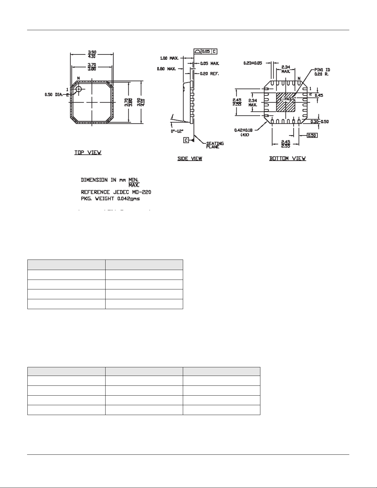
CY8C21x23 Final Data Sheet 4. Packaging Information
51-85203 **
Figure 4-4. 24-Lead (4x4 ) MLF
4.2 Thermal Impedances
Ta ble 4-1. Thermal Impedances per Package
Package Typical θ
8 SOIC
16 SOIC
20 SSOP
24 MLF
* TJ = TA + POWER x θ
186 oC/W
125 oC/W
117 oC/W
40 oC/W
JA
JA
*
4.3 Solder Reflow Peak Temperature
Following is the minimum solder reflow peak temperature to achieve good solderability.
Ta ble 4-2. Solder Reflow Peak Temperature
Package Minimum Peak Temperature* Maximum Peak Temperature
8 SOIC
16 SOIC
20 SSOP
24 MLF
*Higher temperatures may be required based on the solder melting point. Typical temperatures for solder are 220+/-5oC
with Sn-Pb or 245+/-5
o
C with Sn-Ag-Cu paste. Refer to the solder manufacturer specifications.
240oC 260oC
240oC 260oC
240oC 260oC
240oC 260oC
February 25, 2005 Document No. 38-12022 Rev. *G 31
Page 32

5. Ordering Information
C
The following table lists the CY8C21x23 PSoC device’s key package features and ordering codes.
CY8C21x23 PSoC Device Key Features and Ordering Information
Package
8 Pin (150-Mil) SOIC CY8C21123-24SXI 4K 256 No -40°C to +85°C 4 4 6 4 0 No
8 Pin (150-Mil) SOIC
(Tape and Reel)
16 Pin (150-Mil) SOIC CY8C21223-24SXI 4K 256 Yes -40°C to +85°C 4 4 12 8 0 No
16 Pin (150-Mil) SOIC
(Tape and Reel)
20 Pin (210-Mil) SSOP CY8C21323-24PVXI 4K 256 No -40°C to +85°C 4 4 16 8 0 Yes
20 Pin (210-Mil) SSOP
(Tape and Reel)
24 Pin (4x4) MLF CY8C21323-24LFXI 4K 256 Yes -40°C to +85°C 4 4 16 8 0 Yes
24 Pin (4x4) MLF
(Tape and Reel)
CY8C21123-24SXIT 4K 256 No -40°C to +85°C 4 4 6 4 0 No
CY8C21223-24SXIT 4K 256 Yes -40°C to +85°C 4 4 12 8 0 No
CY8C21323-24PVXIT 4K 256 No -40°C to +85°C 4 4 16 8 0 Yes
CY8C21323-24LFXIT 4K 256 Yes -40°C to +85°C 4 4 16 8 0 Yes
Ordering
Code
Flash
(Bytes)
RAM
(Bytes)
Switch Mode
Pump
Range
Temperature
Blocks
Digital PSoC
Blocks
Analog
Digital IO
Pins
Inputs
Analog
Analog
Outputs
5.1 Ordering Code Definitions
Y 8 C 21 xxx-24xx
Package Type: Thermal Rating:
PX = PDIP Pb-Fre e C = Commercia l
SX = SOIC Pb- F r e e I = Indu strial
PVX = SSOP Pb-Free E = Extended
LFX = MLF Pb-Free
AX = TQFP Pb-Free
Speed: 24 MHz
Part Number
Family Code
Technology Code: C = CMOS
Marketing Code: 8 = Cypress MicroSystems
Company ID: CY = Cypress
XRES Pin
February 25, 2005 Document No. 38-12022 Rev. *G 32
Page 33

6. Sales and Service Information
To obtain information about Cypress Semiconductor or PSoC sales and technical support, reference the following information.
Cypress Semiconductor
2700 162nd Street SW, Building D Phone: 800.669.0557
Lynnwood, WA 98037 Facsimile: 425.787.4641
Web Sites: Company Information – http://www.cypress.com
Sales – http://www.cypress.com/aboutus/sales_locations.cfm
Technical Support – http://www.cypress.com/support/login.cfm
6.1 Revision History
Document Title: CY8C21x23 PSoC Mixed- Signal Array Final Data Sheet
Document Number: 38-12022
Revision ECN # Issue Date Origin of Change Description of Change
** 133248 01/28/2004 NWJ New silicon and document (Revision **).
*A 208900 03/05/2004 NWJ
*B
*C
*D
*E
*F 301636 See ECN HMT DC Chip-Level Specification changes. Update links to new CY.com Portal.
*G 324073 See ECN HMT
Distribution: External/Public Posting: None
212081
227321
235973
290991
03/18/2004 NWJ Expand and prepare Preliminary version.
05/19/2004 CMS Team Update specs., data, format.
See ECN SFV
See ECN HMT
Add new part, new package and update all ordering codes to Pb-free.
Updated Overview and Electrical Spec. chapters, along with 24-pin pinout. Added
CMP_GO_EN register (1,64h) to mapping table.
Update data sheet standards per SFV memo. Fix device table. Add part numbers to
pinouts and fine tune. Change 20-pin SSOP to CY8C21323. Add Reflow Temp. table.
Update diagrams and specs.
Obtained clearer 16 SOIC package. Update Thermal Impedances and Solder Reflow
tables. Re-add pinout ISSP notation. Fix ADC type-o. Fix TMP register names. Update
Electrical Specifications. Add CY logo. Update CY copyright. Make data s heet Final.
6.2 Copyrights and Flash Code Protection
Copyrights
© Cypress Semiconducto r Corp. 2004-2005. All rights reserv ed. PSoC™, PSoC Designer™, and P rogrammable System-on-Chip ™ are PSoC-related trademarks o f
Cypress Semiconductor Corp. All other trademarks or registered trademarks referenced herein are property of the respective corporations.
The information contained herein is subject to change without notice. Cypress Se miconductor assumes no responsibility for the use of any circuitry o ther than circui try
embodied in a Cypress Semiconductor product. Nor does it convey or imply any license under patent or other rights. Cypress Semiconductor does not authorize its products
for use as critical components in life-support systems where a malfunction or failure may reasonably be expected to result in significant injury to the user. The inclusion of
Cypress Semiconductor products in life-support systems application implies that the manufacturer assumes all risk of such use and in do ing so indemnifies Cypres s
Semiconductor against all charges. Cypress Semiconductor products are not warranted nor intended to be used for medical, life-support, life-saving, critical control or safety
applicati ons, unless pursuant to an express written agreement with Cypress Semiconductor.
Flash Code Protection
Note the following details of the Flash code protection features on Cypress Semiconductor PSoC devices.
Cypress Semiconductor products meet the specifications contained in their particular data sheets. Cypress Semiconductor believes that its PSoC family of products is one
of the most secure families of its kind on the market today, regardless of how they are used. There may be methods, unknown to Cypress Semiconductor, that can breach
the code protection featu res. Any of thes e methods, to ou r knowledg e, would be dis honest and po ssibly illega l. Neither Cypr ess Semicon ductor nor an y other semi conductor manufacturer can guarantee the security of their code. Code protection does not mean that we are guaranteeing the product as "unbreakable ."
Cypress Semiconductor is willing to work with the customer who is concerned about the integrity of their code. Code protection is constantl y evolving. We at Cypre ss
Semiconductor are committed to continuously improving the code protection features of our products.
February 25, 2005 © Cypress Semiconductor Corp. 2004-2005 — Document No. 38-12022 Rev. *G 33
 Loading...