

Page 1

AN78329 - CapSense® Design Guide
CY8C20xx7/S
Doc. No. 001-78329 Rev. *E
Cypress Semiconductor
198 Champion Court
San Jose, CA 95134-1709
Phone (USA): 800.858.1810
Phone (Intnl): 408.943.2600
www.cypress.com
Page 2

Copyrights
Copyrights
© Cypress Semiconductor Corporation, 2012-2015. The information contained herein is subject to change without notice.
Cypress Semiconductor Corporation assumes no responsibility for the use of any circuitry other than circuitry embodied in a
Cypress product. Nor does it convey or imply any license under patent or other rights. Cypress products are not warranted
nor intended to be used for medical, life support, life saving, critical control or safety applications, unless pursuant to an
express written agreement with Cypress. Furthermore, Cypress does not authorize its products for use as critical
components in life-support systems where a malfunction or failure may reasonably be expected to result in significant injury
to the user. The inclusion of Cypress products in life-support systems application implies that the manufacturer assumes all
risk of such use and in doing so indemnifies Cypress against all charges.
Trademarks
PSoC Designer™, Programmable System-on-Chip™, and SmartSense™ are trademarks and PSoC® and CapSense® are
registered trademarks of Cypress Semiconductor Corp. All other trademarks or registered trademarks referenced herein are
property of the respective corporations.
Source Code
Any Source Code (software and/or firmware) is owned by Cypress Semiconductor Corporation (Cypress) and is protected
by and subject to worldwide patent protection (United States and foreign), United States copyright laws and international
treaty provisions. Cypress hereby grants to licensee a personal, non-exclusive, non-transferable license to copy, use,
modify, create derivative works of, and compile the Cypress Source Code and derivative works for the sole purpose of
creating custom software and or firmware in support of licensee product to be used only in conjunction with a Cypress
integrated circuit as specified in the applicable agreement. Any reproduction, modification, translation, compilation, or
representation of this Source Code except as specified above is prohibited without the express written permission of
Cypress.
Disclaimer
CYPRESS MAKES NO WARRANTY OF ANY KIND, EXPRESS OR IMPLIED, WITH REGARD TO THIS MATERIAL,
INCLUDING, BUT NOT LIMITED TO, THE IMPLIED WARRANTIES OF MERCHANTABILITY AND FITNESS FOR A
PARTICULAR PURPOSE. Cypress reserves the right to make changes without further notice to the materials described
herein. Cypress does not assume any liability arising out of the application or use of any product or circuit described herein.
Cypress does not authorize its products for use as critical components in life-support systems where a malfunction or failure
may reasonably be expected to result in significant injury to the user. The inclusion of Cypress‟ product in a life-support
systems application implies that the manufacturer assumes all risk of such use and in doing so indemnifies Cypress against
all charges.
Use may be limited by and subject to the applicable Cypress software license agreement.
CY8C20xx7/S CapSense® Design Guide Doc. No. 001-78329 Rev. *E 2
Page 3

Contents
1. Introduction .......................................................................................................................................................... 6
1.1 Abstract ....................................................................................................................................................... 6
1.2 Cypress‟s CapSense Documentation Ecosystem ........................................................................................ 6
1.3 CY8C20xx7/S CapSense Family Features .................................................................................................. 8
1.4 Document Conventions ............................................................................................................................. 10
2. CapSense Technology ...................................................................................................................................... 11
2.1 CapSense Fundamentals .......................................................................................................................... 11
2.2 Capacitive Sensing Methods in CY8C20xx7/S .......................................................................................... 12
2.2.1 CapSense Sigma Delta (CSD) ..................................................................................................... 12
2.2.2 CapSense Sigma Delta (CSD) PLUS ........................................................................................... 15
2.2.3 SmartSense_EMCPLUS Auto-Tuning .......................................................................................... 18
2.2.4 Selecting the User Module ............................................................................................................ 19
3. CapSense Design Tools .................................................................................................................................... 20
3.1 Overview ................................................................................................................................................... 20
3.1.1 PSoC Designer and User Modules ............................................................................................... 20
3.1.2 CY8C20xx7/S QuietZone Starter Kit ............................................................................................. 21
3.1.3 CapSense Data Viewing Tools ..................................................................................................... 21
3.2 User Module Overview .............................................................................................................................. 22
3.3 CapSense User Module Global Arrays ...................................................................................................... 22
3.3.1 Raw Count .................................................................................................................................... 23
3.3.2 Baseline ........................................................................................................................................ 23
3.3.3 Difference Count (Signal) ............................................................................................................. 23
3.3.4 Sensor State ................................................................................................................................. 23
3.4 CSD/CSDPLUS User Module Parameters ................................................................................................ 23
3.4.1 User Module High-Level Parameters ............................................................................................ 24
3.4.2 CSD/CSDPLUS User Module Low-Level Parameters .................................................................. 27
3.5 SmartSense_EMCPLUS User Module Parameters ................................................................................... 31
4. CapSense Performance Tuning with User Modules ....................................................................................... 33
4.1 General Considerations ............................................................................................................................. 33
4.2 Tuning the CSD/CSDPLUS User Module .................................................................................................. 35
CY8C20xx7/S CapSense® Design Guide Doc. No. 001-78329 Rev. *E 3
4.1.1 Signal, Noise, and SNR ................................................................................................................ 33
4.1.2 Charge/Discharge Rate ................................................................................................................ 34
4.1.3 Importance of Baseline Update Threshold Verification ................................................................. 35
4.2.1 Recommended C
Value for CSD/CSDPLUS........................................................................... 36
MOD
Page 4

Contents
4.2.2 I
Range .................................................................................................................................... 37
DAC
4.2.3 Autocalibration .............................................................................................................................. 37
4.2.4 I
4.2.5 Compensation I
Value ..................................................................................................................................... 37
DAC
Value ............................................................................................................. 37
DAC
4.2.6 Precharge Source ......................................................................................................................... 37
4.2.7 Prescaler ...................................................................................................................................... 37
4.2.8 Resolution ..................................................................................................................................... 38
4.2.9 Scanning Speed ........................................................................................................................... 38
4.2.10 High-Level API Parameters .......................................................................................................... 39
4.2.11 Set High-Level Parameters ........................................................................................................... 40
4.3 Using the SmartSense_EMCPLUS User Module ...................................................................................... 40
4.3.1 Guidelines for SmartSense_EMC_PLUS ...................................................................................... 40
4.3.2 Understanding the Difference ....................................................................................................... 40
4.3.3 Recommended C
Value for SmartSense_EMC_PLUS ........................................................... 41
MOD
4.3.4 SmartSense_EMCPLUS User Module Parameters ...................................................................... 41
4.3.5 SmartSense_EMCPLUS User Module Specific Guidelines .......................................................... 41
4.3.6 Scan Time of a CapSense Sensor................................................................................................ 42
4.3.7 SmartSense_EMCPLUS Response Time ..................................................................................... 43
4.3.8 Method to Ensure Minimum SNR Using the SmartSense_EMCPLUS UM ................................... 44
4.3.9 Firmware Design Guidelines ......................................................................................................... 45
4.4 Design Migration from CY8C20xx6A/AS to CY8C20xx7/S ........................................................................ 47
4.4.1 Discontinued Support/User Modules ............................................................................................ 47
4.4.2 Improvement and New Features................................................................................................... 47
4.4.3 Pin Compatibility ........................................................................................................................... 47
5. Design Considerations ..................................................................................................................................... 48
5.1 Overlay Selection ...................................................................................................................................... 48
5.2 ESD Protection .......................................................................................................................................... 49
5.2.1 Prevent ......................................................................................................................................... 49
5.2.2 Redirect ................................................................ ........................................................................ 49
5.2.3 Clamp ........................................................................................................................................... 49
5.3 Electromagnetic Compatibility (EMC) Considerations ............................................................................... 49
5.3.1 Radiated Interference ................................................................................................................... 49
5.3.2 Radiated Emissions ...................................................................................................................... 50
5.3.3 Conducted Immunity and Emissions ............................................................................................. 50
5.4 Software Filtering ....................................................................................................................................... 50
5.5 Power Consumption .................................................................................................................................. 51
5.5.1 System Design Recommendations ............................................................................................... 51
5.5.2 Sleep-Scan Method ...................................................................................................................... 51
5.5.3 Response Time versus Power Consumption ................................................................................ 51
5.5.4 Measuring Average Power Consumption ..................................................................................... 52
5.6 Pin Assignments ........................................................................................................................................ 52
5.7 GPIO Load Transient ................................................................................................................................. 53
5.7.1 Hardware Guidelines to Reduce GPIO Load Transient Noise ...................................................... 54
5.7.2 Firmware Guidelines to Compensate GPIO Load Transient Noise ............................................... 55
5.8 PCB Layout Guidelines ............................................................................................................................. 57
6. Liquid-Tolerant Design Considerations .......................................................................................................... 58
CY8C20xx7/S CapSense® Design Guide Doc. No. 001-78329 Rev. *E 4
Page 5

Contents
6.1 Shield Electrode and Guard Sensor .......................................................................................................... 58
6.1.1 Shield ............................................................................................................................................ 58
6.1.2 Guard Sensor ............................................................................................................................... 61
6.2 Design Recommendations ........................................................................................................................ 63
7. Proximity Sensing Design Considerations ..................................................................................................... 64
7.1 Types of Proximity Sensors ....................................................................................................................... 64
7.1.1 Button ........................................................................................................................................... 64
7.1.2 Wire .............................................................................................................................................. 64
7.1.3 PCB Trace .................................................................................................................................... 64
7.1.4 Sensor Ganging ............................................................................................................................ 64
7.2 Design Recommendations ........................................................................................................................ 65
8. Low-Power Design Considerations ................................................................................................................. 66
8.1 Additional Power Saving Techniques ........................................................................................................ 66
8.1.1 Set Drive Modes to Analog HI-Z ................................................................................................... 66
8.1.2 Putting it All Together ................................................................................................................... 67
8.1.3 Recommended I2C Slave Implementation in Sleep Mode ............................................................ 67
8.1.4 Sleep Mode Complications ........................................................................................................... 67
8.1.5 Pending Interrupts ........................................................................................................................ 67
8.1.6 Global Interrupt Enable ................................................................................................................. 68
8.2 Post Wakeup Execution Sequence ........................................................................................................... 68
8.2.1 PLL Mode Enabled ....................................................................................................................... 68
8.2.2 Execution of Global Interrupt Enable ............................................................................................ 68
8.2.3 Recommended I2C Slave Implementation in Sleep Mode ............................................................ 68
8.2.4 Sleep Timer .................................................................................................................................. 69
9. Resources .......................................................................................................................................................... 70
9.1 Website ..................................................................................................................................................... 70
9.2 Datasheet ................................................................................................ .................................................. 70
9.3 Technical Reference Manual ..................................................................................................................... 70
9.4 Development Kits ...................................................................................................................................... 71
9.4.1 CY8C20xx7/S QuietZone Starter Kit ............................................................................................. 71
9.4.2 Universal CapSense Controller Kit ............................................................................................... 71
9.4.3 Universal CapSense Module Boards ............................................................................................ 71
9.5 Sample Board Files ................................................................................................................................... 72
9.6 PSoC Programmer .................................................................................................................................... 74
9.7 CapSense Data Viewing Tools .................................................................................................................. 74
9.8 PSoC Designer .......................................................................................................................................... 74
9.9 Code Examples ......................................................................................................................................... 74
9.10 Design Support .......................................................................................................................................... 74
Revision History ......................................................................................................................................................... 75
CY8C20xx7/S CapSense® Design Guide Doc. No. 001-78329 Rev. *E 5
Page 6

1. Introduction
1.1 Abstract
This document provides design guidance for implementing capacitive sensing (CapSense) functionality with the
CY8C20xx7/S family of CapSense controllers. The following topics are covered in this guide:
Features of the CY8C20xx7/S family of CapSense controllers
CapSense principles of operation
Introduction to CapSense design tools
Guide to tune the CapSense system for optimal performance
System electrical and mechanical design considerations for CapSense
Low-power design considerations for CapSense
Additional resources and support for designing CapSense into your system
1.2 Cypress’s CapSense Documentation Ecosystem
Figure 1-1 and Table 1-1 summarize the Cypress CapSense documentation ecosystem. These resources allow
implementers to quickly access the information needed to successfully complete a CapSense product design.
Figure 1-1 shows the typical flow of a product design cycle with capacitive sensing; the information in this guide is
most pertinent to the topics highlighted in green. Table 1-1 provides links to the supporting documents for each of the
numbered tasks in Figure 1-1.
CY8C20xx7/S CapSense® Design Guide Doc. No. 001-78329 Rev. *E 6
Page 7

Introduction
3. CapSense device selection based
on needed functionality
2. Specify system requirements and
characteristics
11. Preproduction build (prototype)
12. Test and evaluate system functionality and
CapSense performance
Performance
satisfactory
13. Production
Yes
No
= Topics covered in this document
1. Understanding CapSense technology
4. Mechanical
design
5. Schematic
capture and
PCB layout
Design for CapSense
9. Programming PSoC
†
10. CapSense
Configuration*
6. PSoC Designer project
creation†
7. Firmware
development†
8. CapSense tuning†
*
†
= Applicable to MBR family of devices only
= Applicable to programmable devices only
Figure 1-1. Typical CapSense Product Design Flow
CY8C20xx7/S CapSense® Design Guide Doc. No. 001-78329 Rev. *E 7
Page 8

Introduction
Numbered Design Task
in Figure 1-1
Supporting Cypress CapSense Documentation
1
● Getting Started with CapSense
2
● Getting Started with CapSense
● CY8C20xx7/S CapSense Device Datasheet
3
● Getting Started with CapSense
● CY8C20xx7/S CapSense Design Guide (this document)
4
● Getting Started with CapSense
5
● Getting Started with CapSense
6
● PSoC® Designer™ User Guides
7
● Assembly Language User Guide
● C Language Compiler User Guide
● CapSense Code Examples
● PSoC CY8C20xx7/S Technical Reference Manual
8
● PSoC Family-Specific CapSense Design Guide (this document)
● PSoC Family-Specific CapSense User Module Datasheets (CSD, CSDPLUS, and
SmartSense_EMC_PLUS)
● PSoC CY8C20xx7/S Technical Reference Manual
● AN2397 -CapSense Data Viewing Tools
9
● Programmer User Guide
● MiniProg3 User Guide
● ISSP Programming Specifications - CY8C20045, CY8C20055, CY8C20065,
CY8C20xx6A,CY8C20xx7
● AN59389 - Host Sourced Serial Programming for CY8C20xx6A, CY8C20xx6AS, CY8C20xx6L, and
CY8C20xx7/S
11
● CY8C20xx7/S CapSense Design Guide (this document)
● CapSense Code Examples
Table 1-1. Cypress Documents Supporting Numbered Design Tasks of Figure 1-1
1.3 CY8C20xx7/S CapSense Family Features
Cypress‟s CY8C20xx7/S is a low-power, high-performance, programmable CapSense controller family that features:
Advanced Touch Sensing Features
Programmable capacitive sensing elements
Supports a combination of CapSense buttons, sliders, and proximity sensors
Integrated API to implement buttons and sliders
Supports up to 31a capacitive sensors or six slidersb
Supports parasitic sensor capacitance range of 5 pF to 45 pF
SmartSense™ Auto-tuning enables fast time to market
Sets and monitors tuning parameters automatically at power on and at runtime
Design portability – self-tunes for changes in user interface design
Environmental compensation during runtime
Detects touches as low as 0.1 pF
Enhanced noise immunity and robustness
a
It is assumed that two pins are used for I
b
See the CY8C20xx7/S datasheet for more information.
CY8C20xx7/S CapSense® Design Guide Doc. No. 001-78329 Rev. *E 8
2
C communication and one pin is used for C
connection.
MOD
Page 9

Introduction
SmartSense_EMCPLUS compensates for environment and noise variations automatically
SmartSense_EMCPLUS offers superior noise immunity for applications with challenging conducted and
radiated noise conditions
Internal regulator provides stability against power supply noise and ripple up to 500 mV of supply VDD ripple
acceptable
Integrated API of software filters for SNR improvement
Ultra low power consumption
Three different power modes for optimized power consumption
Active, sleep, and deep-sleep modes (deep-sleep current: 100 nA)
28 μA per sensor at 125 ms wake from sleep rate
Driven shield available on five GPIO pins
Delivers best-in-class water tolerant designs
Robust proximity sensing in the presence of metal objects
Supports longer trace lengths
Maximum load of 100 pF (3 MHz)
Device Features
High-performance, low-power M8C Harvard-architecture processor
Up to 4 MIPS with 24-MHz internal clock
Flexible on-chip memory
Up to 32 KB of flash and 2 KB of SRAM
Emulated EEPROM supported
Precision, programmable clocking
Internal main oscillator (IMO): 6/12/24 MHz ± 5%
Option for precision 32-kHz external crystal oscillator
Enhanced general-purpose input/output (GPIO) features
34 GPIOs with programmable pin configuration.
25 mA sink current/GPIO and 120 mA total sink current/device
Internal restive pull-up, HI-Z, open-drain, and strong drive modes on all GPIOs
Peripheral features
Three 16-bit timers
I2C - master (100 kHz) and slave (400 kHz)
SPI - master and slave - configurable range of 46.9 kHz to 12 MHz
10-bit incremental ADC - 0 to 1.2-V input range
Operating conditions
Wide operating voltage: 1.71 V to 5.5 V
Temperature range: –40 °C to +85 °C
CY8C20xx7/S CapSense® Design Guide Doc. No. 001-78329 Rev. *E 9
Page 10

Introduction
Convention
Usage
Courier New
Displays file locations, user entered text, and source code:
C:\ ...cd\icc\
Italics
Displays file names and reference documentation:
Read about the sourcefile.hex file in the PSoC Designer User Guide.
[Bracketed, Bold]
Displays keyboard commands in procedures:
[Enter] or [Ctrl] [C]
File > Open
Represents menu paths:
File > Open > New Project
Bold
Displays commands, menu paths, and icon names in procedures:
Click the File icon and then click Open.
Times New Roman
Displays an equation:
2 + 2 = 4
Text in gray boxes
Describes Cautions or unique functionality of the product.
1.4 Document Conventions
CY8C20xx7/S CapSense® Design Guide Doc. No. 001-78329 Rev. *E 10
Page 11

2. CapSense Technology
2.1 CapSense Fundamentals
CY8C20xx7/S
C
MOD
Sensor 1
C
X,1
Sensor 2
C
X,2
Sensor 3
C
X,3
Sensor 4
C
X,4
Sensor n
C
X,n
CapSense is a touch-sensing technology, which works by measuring the capacitance of each I/O pin on the
CapSense controller that has been designated as a sensor. As shown in Figure 2-1, the total capacitance on each
sensor pin can be modeled as equivalent lumped capacitors with values of CX,1 through CX,n for a design with n
sensors. The circuitry internal to the CY8C20xx7/S device converts the magnitude of each CX into a digital code that
is stored for post processing. The other component, C
will be discussed in more detail in Capacitive Sensing Methods in CY8C20xx7/S.
Figure 2-1. CapSense Implementation in a CY8C20xx7/S PSoC Device
, is used by the CapSense controller‟s internal circuitry and
MOD
As shown in Figure 2-1, each sensor I/O pin is connected to a sensor pad by traces, vias, or both, as necessary. The
overlay is a nonconductive cover over the sensor pad that constitutes the product‟s touch interface. When a finger
comes into contact with the overlay, the conductivity and mass of the body effectively introduces a grounded
conductive plane parallel to the sensor pad. This is represented in Figure 2-2. This arrangement constitutes a parallel
plate capacitor, whose capacitance is given by:
0
=
Where:
CF = The capacitance added by a finger in contact with the overlay over a sensor
ε
= Free space permittivity
0
ε
= Dielectric constant (relative permittivity) of overlay
r
A = Area of finger and sensor pad overlap
D = Overlay thickness
Equation 2-1
CY8C20xx7/S CapSense® Design Guide Doc. No. 001-78329 Rev. *E 11
Page 12

CapSense Technology
Figure 2-2. Section of Typical CapSense PCB with the Sensor Being Activated by a Finger
In addition to the parallel plate capacitance, a finger in contact with the overlay causes electric field fringing between
itself and other conductors in the immediate vicinity. The effect of these fringing fields is typically minor compared to
that of the parallel plate capacitor and can usually be ignored.
Even without a finger touching the overlay, the sensor I/O pin has some parasitic capacitance (CP). CP results from
the combination of the CapSense controller internal parasitics and electric field coupling between the sensor pad,
traces, and vias, and other conductors in the system such as ground plane, other traces, any metal in the product‟s
chassis or enclosure, and so on. The CapSense controller measures the total capacitance (CX) connected to a
sensor pin.
When a finger is not touching a sensor:
= Equation 2-2
With a finger on the sensor pad, CX equals the sum of CP and CF:
= + Equation 2-3
In general, CP is an order of magnitude greater than CF. CP usually ranges from 10 pF to 20 pF, but in extreme cases
can be as high as 50 pF. CF usually ranges from 0.1 pF to 0.4 pF. The magnitude of CP is of critical importance when
tuning a CapSense system and is discussed in CapSense Performance Tuning with User Modules.
2.2 Capacitive Sensing Methods in CY8C20xx7/S
CY8C20xx7/S devices support CSD, CSDPLUS, and SmartSense_EMCPLUS CapSense methods for converting
sensor capacitance (CX) into digital counts. The CSDPLUS method is the superset of the CSD method and has
several improvements when compared to CSD. These two methods are implemented in the hardware. The
SmartSense_EMCPLUS uses the autotuning algorithm implemented in firmware to automatically tune all the
CSDPLUS parameters. The CSD, CSDPLUS, and SmartSense_EMCPLUS methods are implemented in the form of
a PSoC Designer User Module and are described in the following sections.
2.2.1 CapSense Sigma Delta (CSD)
Figure 2-3 shows a block diagram of the CSD method for converting sensor capacitance (CX) into digital counts. This
method can be conceptually broken into two blocks – switched-capacitor input, which converts capacitance to current
and sigma delta converter, which converts current to digital counts. These blocks are explained in the following
sections.
CY8C20xx7/S CapSense® Design Guide Doc. No. 001-78329 Rev. *E 12
Page 13

CapSense Technology
Sigma Delta
Modulator
High Z
input
R
BUS
Modulation
I
DAC
C
X
Precharge
clock
CY8C20xx7/S
V
REF
Switched-capacitor input
circuit converts
capacitance to current
External Connection
C
MOD
2.2nF/X7R/5V
Sigma delta converter converts current to digital counts
Analog Mux
Bus
Sw2
Sw1
Analog Mux Bus
(AMUXBUS)
Discharge
Clock
Break-
Before-Make
Circuitry
Pin
C
X
Sw2
Sw1
Figure 2-3. CSD Block Diagram
2.2.1.1 Switched-Capacitor Input
The CSD method in the CY8C20xx7/S device incorporates CX into a switched capacitor circuit, as Figure 2-3 shows.
Figure 2-4. Pin Configured as Switched-Capacitor Input
Two non-overlapping, out-of-phase clocks of frequency FSW (see Figure 2-6) control the switches Sw1 and Sw2. The
continuous switching of Sw1 and Sw2 forms an equivalent resistance RS, as Figure 2-5 shows. The value of the
equivalent resistance RS is:
CX F
1
Equation 2-4
SW
RS=
Where:
CX = Sensor capacitance
FSW = Frequency of the switching clock
CY8C20xx7/S CapSense® Design Guide Doc. No. 001-78329 Rev. *E 13
Page 14

CapSense Technology
C
X
R
S
AMUXBUS
Sw
1
Sw
2
AMUXBUS
I
SENSOR
I
SW
I
SENSOR
V
t
V
REF
(1V)
0
TSW = 1/F
SW
Sw2 CLOSED
Sw1 OPEN
Sw2 OPEN
Sw1 CLOSED
Figure 2-5. Switched-Capacitor Input Sinking Current from AMUXBUS
The sigma delta converter maintains the voltage of AMUXBUS at a constant V
(this process is explained in Sigma
REF
Delta Converter). Figure 2-6 shows the voltage waveform across the sensor capacitance. Driving switches Sw1 and
Sw2 through non-overlapping precharge clocks thus results in an average current sink (I
as Equation 2-5 shows. The magnitude of I
I
SENSOR
= V
REFRS
= CX FSWV
Equation 2-5
REF
is directly proportional to the magnitude of CX.
SENSOR
) from the AMUXBUS
SENSOR
Figure 2-6. Voltage across Sensor Capacitance (CX)
2.2.1.2 Sigma Delta Converter
The sigma delta converter converts the input current to a corresponding digital count. It consists of a sigma delta
modulator and one current-sourcing digital-to-analog converter (I
The sigma delta modulator controls the 8-bit I
I
and is referred as “I
DAC
external integrating capacitor C
” or “modulation I
DAC
, as Figure 2-3 on page 13 shows. The recommended value of C
MOD
The sigma delta modulator switches the modulation I
across C
, to maintain the C
MOD
voltage at V
MOD
current in an on/off manner. This I
DAC
in this document. The sigma delta converter also requires an
DAC”
ON or OFF corresponding to the small voltage variations
DAC
.
REF
In maintaining the average AMUX voltage at a steady state value (V
average charge current (I
DAC
) to I
by controlling the modulation bit stream duty cycle. The sigma delta converter
SENSOR
stores the bit stream over the duration of a sensor scan and the accumulated result is a digital output value, known as
raw count, which is proportional to CX.
The sigma delta converter can operate from 9-bit to 16-bit resolutions. If „N‟ is the resolution of the sigma delta
converter and I
raw count = (2
The raw count is interpreted by high-level algorithms to resolve the sensor state and detect touches. Figure 2-7 plots
the CSD raw counts from a number of consecutive scans during which the sensor is touched and then released by a
finger. As explained in CapSense Fundamentals, the finger touch causes CX to increase by CF, which in turn causes
is the value of the modulation I
DAC
V
N
1)
CY8C20xx7/S CapSense® Design Guide Doc. No. 001-78329 Rev. *E 14
REF FSW CX
I
DAC
current, the approximate equation for the raw count is
DAC
Equation 2-6
), as Figure 2-3 on page 13 shows.
DAC
is known as the modulation
DAC
), the sigma delta converter matches the
REF
is 2.2 nF.
MOD
Page 15

CapSense Technology
raw counts to increase proportionally. By comparing the shift in steady state raw count level to a predetermined
threshold, the high-level algorithms can determine whether the sensor is in the ON (touch) or OFF (no touch) state.
Figure 2-7. CSD Raw Counts during a Finger Touch
The hardware parameters or the CSD/CSDPLUS User Module Low-Level Parameters such as I
and FSW, and the
DAC
firmware parameters or the User Module High-Level Parameters should be tuned to optimum values for reliable touch
detection. For a detailed discussion on tuning, see CapSense Performance Tuning with User Modules.
2.2.2 CapSense Sigma Delta (CSD) PLUS
Figure 2-8 shows a block diagram of the CSDPLUS method for converting sensor capacitance (CX) into digital
counts. The main difference between CSDPLUS and CSD method is the number of I
I
and the CSD uses a single I
DACs
DAC
.
used; CSDPLUS uses two
DACs
The CSDPLUS method can be conceptually broken into two blocks – switched-capacitor input, which converts
capacitance to current and sigma delta converter, which converts current to digital counts. Each block is explained in
the following sections.
CY8C20xx7/S CapSense® Design Guide Doc. No. 001-78329 Rev. *E 15
Page 16

CapSense Technology
Sigma Delta
Modulator
High Z
input
R
BUS
Modulation
I
DAC
Compensation
I
DAC
C
X
Precharge
clock
CY8C20xx7/S
V
REF
Switched-capacitor input
circuit converts
capacitance to current
External Connection
C
MOD
2.2 nF/X7R/5 V
Sigma delta converter converts current to digital counts
Analog Mux
Bus
Sw2
Sw1
Analog Mux Bus
(AMUXBUS)
Discharge
Clock
Break-
Before-Make
Circuitry
Pin
C
X
Sw2
Sw1
Figure 2-8. CSDPLUS Block Diagram
2.2.2.1 Switched-Capacitor Input
The CSDPLUS method in CY8C20xx7/S devices incorporates CX into a switched-capacitor circuit, as Figure 2-9
shows.
Figure 2-9. Pin Configured as Switched-Capacitor Input
Two non-overlapping, out-of-phase clocks of frequency FSW (see Figure 2-11) control switches Sw1 and Sw2. The
continuous switching of Sw1 and Sw2 forms an equivalent resistance RS, as Figure 2-10 shows. The value of the
equivalent resistance RS is:
RS=
1
Equation 2-7
CX F
SW
Where:
CX = Sensor capacitance
FSW = Frequency of the switching clock
CY8C20xx7/S CapSense® Design Guide Doc. No. 001-78329 Rev. *E 16
Page 17

CapSense Technology
C
X
R
S
AMUXBUS
Sw
1
Sw
2
AMUXBUS
I
SENSOR
I
SW
I
SENSOR
V
t
V
REF
(1V)
0
TSW = 1/F
SW
Sw2 CLOSED
Sw1 OPEN
Sw2 OPEN
Sw1 CLOSED
raw count = (2
N
1)
V
REF FSW
I
DAC
C
X
(2N 1)
I
COMP
I
DAC
Equation 2-9
Figure 2-10. Switched Capacitor Input Sinking Current from AMUXBUS
The sigma delta converter maintains the voltage of AMUXBUS at a constant V
(this process is explained in Sigma
REF
Delta Converter). Figure 2-11 shows the voltage waveform across the sensor capacitance. Driving switches Sw1 and
Sw2 through non-overlapping precharge clocks thus results in an average current sink (I
as Equation 2-8 shows. The magnitude of I
I
SENSOR
= V
REFRS
= CX FSWV
Equation 2-8
REF
is directly proportional to the magnitude of CX.
SENSOR
) from the AMUXBUS
SENSOR
Figure 2-11. Voltage across Sensor Capacitance (CX)
2.2.2.2 Sigma Delta Converter
The sigma delta converter converts the input current to a corresponding digital count. It consists of a sigma delta
modulator and two current-sourcing digital-to-analog converters (I
The sigma delta modulator controls the one 7-bit I
modulation I
compensation I
and is referred as “I
DAC
, is either always ON or always OFF. This I
DAC
” or “modulation I
DAC
current in an on/off manner. This I
DAC
DAC”
document.
The sigma delta converter also requires an external integrating capacitor C
recommended value of C
corresponding to the small voltage variations across C
is 2.2 nF. The sigma delta modulator switches the modulation I
MOD
, to maintain the C
MOD
In maintaining the average AMUX voltage at a steady state value (V
average charge current (I
DAC
) to I
by controlling the modulation bit stream duty cycle. The sigma delta converter
SENSOR
stores the bit stream over the duration of a sensor scan and the accumulated result is a digital output value, known as
raw count, which is proportional to CX.
The sigma delta converter can operate from 9-bit to 16-bit resolutions. If „N‟ is the resolution of the sigma delta
converter, I
is the value of the modulation I
DAC
current and I
DAC
equation for the raw count is
Note that raw count values are always positive. Thus, I
CY8C20xx7/S CapSense® Design Guide Doc. No. 001-78329 Rev. *E 17
should always be less than 2N V
COMP
), as Figure 2-8 on page 16 shows.
DACs
in this document. The other 7-bit I
is referred as “Compensation I
DAC
, as Figure 2-8 on page 16 shows. The
MOD
voltage at V
MOD
), the sigma delta converter matches the
REF
is the compensation I
COMP
REF
current, the approximate
DAC
REF FSW
is known as the
DAC
, known as the
DAC
” or “I
DAC
COMP
ON or OFF
DAC
.
.
” in this
Page 18

CapSense Technology
The raw count is interpreted by high-level algorithms to resolve the sensor state and detect touches. Figure 2-12 plots
the CSD raw counts from a number of consecutive scans during which the sensor is touched and then released by a
finger. As explained in CapSense Fundamentals, the finger touch causes CX to increase by CF, which in turn causes
raw counts to increase proportionally. By comparing the shift in steady state raw count level to a predetermined
threshold, the high-level algorithms can determine whether the sensor is in the ON (touch) or OFF (no touch) state.
Figure 2-12. CSD Raw Counts during a Finger Touch
The hardware parameters or the CSD/CSDPLUS User Module Low-Level Parameters such as I
and the firmware parameters or the User Module High-Level Parameters should be tuned to optimum values for
reliable touch detection. For a detailed discussion on tuning, see CapSense Performance Tuning with User Modules.
DAC, ICOMP
, and FSW,
2.2.3 SmartSense_EMCPLUS Auto-Tuning
Tuning the touch-sensing user interface is a critical step in ensuring proper system operation and a pleasant user
experience. The typical design flow involves tuning the sensor interface in the initial design phase, during system
integration, and finally production fine-tuning before the production ramp. Tuning is an iterative process and can be
time consuming. SmartSense_EMCPLUS Auto-Tuning was developed to simplify the user interface development
cycle. The process is easy to use and significantly reduces the design cycle time by eliminating the tuning process
throughout the entire product development cycle, from prototype to mass production. SmartSense_EMCPLUS tunes
each CapSense sensor automatically at power-up and then monitors and maintains optimum sensor performance
during runtime. This technology adapts for manufacturing variation in PCBs, overlays, and noise generators such as
LCD inverters, AC line noise, and switch-mode power supplies, and automatically tunes them out.
2.2.3.1 Process Variation
The SmartSense_EMCPLUS User Module (UM) for the CY8C20xx7/S is designed to work with sensor parasitic
capacitance in the range 5 pF to 45 pF, (typical sensor CP values are in the range 10 pF to 20 pF). The sensitivity
parameter for each sensor is set automatically, based on the characteristics of that particular sensor. This improves
the yield in mass production, because consistent response is maintained from every sensor regardless of CP variation
between sensors within the specified range (5 pF to 45 pF). Parasitic capacitance of the individual sensors can vary
due to PCB layout, PCB manufacturing process variation, or with vendor-to-vendor PCB variation within a
multisourced supply chain. The sensitivity of a sensor depends on its parasitic capacitance; higher CP values
decrease the sensor sensitivity and result in decreased finger touch signal amplitude. In some cases, the change in
CP value detunes the system, resulting in less than optimum sensor performance (either too sensitive or not sensitive
enough) or worst case, a nonoperational sensor. In either situation, you must retune the system, and in some cases
requalify the UI subsystem. SmartSense_EMCPLUS Auto-Tuning solves these issues.
SmartSense_EMCPLUS Auto-Tuning makes platform designs possible. Imagine the capacitive touch-sensing
multimedia keys in a laptop computer; the spacing between the buttons depends on the size of the laptop and
keyboard layout. In this example, the wide-screen machine has larger spaces between the buttons than a standardscreen model. More space between buttons means increased trace length between the sensor and the CapSense
controller, which leads to higher parasitic capacitance of the sensor. This means that the parasitic capacitance of the
CapSense buttons can be different in different models (Figure 2-13 and Figure 2-14) of the same platform design.
Though the functionality of these buttons is the same for all laptop models, the sensors must be tuned for each
model. SmartSense_EMCPLUS enables you to do platform designs using the recommended best practices shown in
the PCB Layout in Getting Started with CapSense, knowing the tuning will be done efficiently and automatically.
CY8C20xx7/S CapSense® Design Guide Doc. No. 001-78329 Rev. *E 18
Page 19

CapSense Technology
Feasibility
Study
Schematics
Design
PCB Layout
Design
Mechanical Design
Review
System
Integration
Re-tuning for any
changes
Tuning process
Production Fine
Tuning
Design
Validation
Production
Typical Capacitive User Interface Design Cycle
Firmware
Development
Feasibility
Study
Schematics
Design
PCB Layout
Design
Mechanical Design
Review
System
Integration
Design
Validation
Production
SmartSense-based Capacitive User Interface Design Cycle
Firmware
Development
Figure 2-13. Design of Laptop Multimedia Keys for a 21-Inch Model
Figure 2-14. Design of Laptop Multimedia Keys for a 15-Inch Model with Identical Functionality and Button Size
2.2.3.2 Reduced Design Cycle Time
Usually, the most time-consuming task for a capacitive sensor interface design is firmware development and sensor
tuning. With a typical touch-sensing controller, the sensor must be retuned when the same design is ported to
different models or when there are changes in the mechanical dimensions of the PCB or the sensor PCB layout. A
design with SmartSense_EMCPLUS solves these challenges because it needs less firmware development effort, no
tuning, and no retuning. This makes a typical design cycle much faster. Figure 2-15 compares the design cycles of a
typical touch-sensing controller and a SmartSense_EMC_PLUS-based design.
Figure 2-15. Typical Capacitive Interface Design Cycle Comparison
2.2.4 Selecting the User Module
The SmartSense_EMCPLUS eliminates the tuning process that is required by CSD and CSDPLUS UM. It is
recommended to use SmartSense_EMCPLUS to simplify the CapSense design process. However, there may be
instances where the sensor parameters such as resolution and prescaler need to be controlled to optimize device
power consumption or detect touch for a sensor with high CP. In such cases, use the CSD/CSDPLUS UM.
The following are the advantages of the CSDPLUS UM when compared to CSD:
CSDPLUS UM provides higher SNR for a given sensor resolution (or scan time).
CSDPLUS UM requires less time to scan a sensor to achieve the same SNR. Because of the short scan time,
the average power consumptiona of the CapSense device with CSDPLUS UM will be lower than the CSD UM
when they are tuned to achieve the same SNR.
However, if the sensor CP is below 10 pF, the CSDPLUS UM provides lower SNR when compared to the CSD UM
and it is recommended to use the CSD UM instead of the CSDPLUS UM.
Note: When I
a
Here the device is assumed to enter sleep mode after scanning the sensor and wakeup periodically to reduce the device power
consumption.
is set to „0‟, the CSDPLUS UM behavior will be the same as the CSD UM.
COMP
CY8C20xx7/S CapSense® Design Guide Doc. No. 001-78329 Rev. *E 19
Page 20

3. CapSense Design Tools
3.1 Overview
Cypress offers a full line of hardware and software tools for developing your CapSense capacitive touch-sensing
application. See Resources for ordering information.
3.1.1 PSoC Designer and User Modules
Cypress‟s exclusive integrated design environment, PSoC Designer, allows you to configure analog and digital
blocks, develop firmware, and tune and debug your design. Applications are developed in a drag-and-drop design
environment using a library of user modules. User modules are configured either through the Device Editor GUI or by
writing into specific registers with firmware. PSoC Designer comes with a built-in C compiler and an embedded
programmer. A pro compiler is available for complex designs.
The CSD and CSDPLUS User Module implements capacitive touch sensors using switched-capacitor circuitry, an
analog multiplexer, a comparator, digital counting functions, and high-level software routines (APIs). User modules for
other analog and digital peripherals are available to implement additional functionality such as I2C, SPI, TX8, and
timers.
Figure 3-1. PSoC Designer Device Editor
CY8C20xx7/S CapSense® Design Guide Doc. No. 001-78329 Rev. *E 20
Page 21

CapSense Design Tools
3.1.1.1 Getting Started with CapSense User Modules
To create a new CY8C20xx7/S project in PSoC Designer:
1. Create a new PSoC Designer project with CY8C20xx7/S as the target device.
2. Select and place the CSDPLUS/SmartSense_EMCPLUS User Module.
3. Right-click the user module to access the User Module wizard.
4. Set button sensor count, slider configuration, pin assignments, and associations.
5. Set pins and global user module parameters.
6. Generate the application and switch to the Application Editor.
7. Adapt sample code from the user module datasheet to implement buttons or sliders.
For a detailed procedure for creating a PSoC Designer project and configuring the User Module wizard, refer to the
datasheet of the specific user module. For code examples on CapSense user modules, see Code Examples.
3.1.2 CY8C20xx7/S QuietZone Starter Kit
The CY8C20xx7/S QuietZone Starter Kit features simple plug-in hardware to make prototyping easy. The kit is
available from our module partner ArtaFlex at the following link: www.artaflexmodules.com/quietzone
Figure 3-2. CY8C20xx7/S QuietZone Starter Kit
3.1.3 CapSense Data Viewing Tools
Many times during CapSense design, you will want to monitor CapSense data (raw counts, baseline, difference
counts, and so on) for tuning and debugging purposes. There are two CapSense data viewing tools, MultiChart and
Bridge Control Panel. These tools are explained in the application note AN2397 – CapSense Data Viewing Tools.
CY8C20xx7/S CapSense® Design Guide Doc. No. 001-78329 Rev. *E 21
Page 22

CapSense Design Tools
Raw Count
Difference
Count
3.2 User Module Overview
Figure 3-3. User Module Block Diagram
User modules contain an entire CapSense system from physical sensing to data processing. The behavior of the user
module is defined using a variety of parameters. These parameters affect different parts of the sensing system and
can be separated into low-level and high-level parameters that communicate with one another using global arrays.
Low-level parameters define the behavior of the sensing method at the physical layer and relate to the conversion
from capacitance to raw count such as the speed and resolutions for scanning sensors. Low-level parameters are
unique to each type of sensing method and are described in CSD/CSDPLUS User Module Low-Level Parameters
and SmartSense_EMCPLUS User Module Parameters.
High-level parameters, such as debounce counts and noise thresholds, define how the raw counts are processed to
produce information such as the sensor ON/OFF state and the estimated finger position on a slider. These
parameters are the same for all sensing methods and are described in User Module High-Level Parameters.
3.3 CapSense User Module Global Arrays
Before learning CapSense User Module parameters, you must be familiar with certain global arrays used by the
CapSense system. These arrays should not be altered manually, but may be inspected for debugging purposes.
Figure 3-4. Raw Count, Baseline, Difference Count, and Sensor State
CY8C20xx7/S CapSense® Design Guide Doc. No. 001-78329 Rev. *E 22
Page 23

CapSense Design Tools
3.3.1 Raw Count
The hardware circuit in the CapSense controller measures the sensor capacitance CX. The circuit stores the result in
a digital form called raw count upon calling the user module API UMname_ScanSensor(), where UMname can be
CSD, CSDPLUS, or SmartSenseEMC_PLUS.
The raw count of a sensor is proportional to its sensor capacitance. Raw count increases as the sensor capacitance
value increases.
The raw count values of sensors are stored in the UMname_waSnsResult[] integer array. This array is defined in the
header file UMname.h.
3.3.2 Baseline
Baseline can be considered as the raw count value corresponding to the parasitic capacitance of sensor, CP. Gradual
environmental changes such as temperature and humidity affect the sensor CP and hence CX, which results in
variations in the raw counts.
The user module uses a complex baselining algorithm to compensate for these variations. The algorithm uses
baseline variables to accomplish this. The baseline variables keep track of any gradual variation in raw count values.
Essentially, the baseline variables hold the output of a digital low-pass filter to which raw count values are input.
The baselining algorithm is executed by the user module API UMname_UpdateSensorBaseline, where UMname can
be CSD, CSDPLUS, or SmartSense_EMC_PLUS.
The baseline values of sensors are stored in UMname_waSnsBaseline[] integer array. This array is defined in the
header file UMname.h.
3.3.3 Difference Count (Signal)
The difference count, which is also known as the signal of a sensor, is defined as the difference in counts between a
sensor‟s raw count and baseline values. When the sensor is inactive, the difference count is zero. Activating sensors
(by touching) results in a positive difference count value.
The difference count values of sensors are stored in the UMname_waSnsDiff[] integer array, where UMname can be
CSD, CSDPLUS, or SmartSense_EMC_PLUS. This array is defined in the header file UMname.h.
Difference count variables are updated by the user module API UMname_UpdateSensorBaseline().
3.3.4 Sensor State
Sensor state represents the active/inactive status of the physical sensors. The state of the sensor changes from 0 to
1 upon finger touch and returns to 0 upon finger release.
Sensor states are stored in a byte array named UMname_baSnsOnMask[] array, where UMname can be CSD,
CSDPLUS, or SmartSense_EMCPLUS. This array is defined in the header file UMname.h. Each array element stores
the sensor state of eight consecutive sensors.
Sensor states are updated by the user module API UMname_bIsAnySensorActive().
3.4 CSD/CSDPLUS User Module Parameters
The CSD/CSDPLUS User Module parameters are classified into high-level and low-level parameters. See Figure 3-5
for a list of CSDPLUS user module parameters and how they are classified. The only difference between the CSD
and CSDPLUS UM parameter window is that the CSD UM does not have Compensation iDAC Value.
CY8C20xx7/S CapSense® Design Guide Doc. No. 001-78329 Rev. *E 23
Page 24

CapSense Design Tools
Figure 3-5. PSoC Designer – CSDPLUS Parameter Window
3.4.1 User Module High-Level Parameters
3.4.1.1 Finger Threshold
The Finger Threshold parameter is used by the user module to judge the active/inactive state of a sensor. If the
difference count value of a sensor is greater than the finger threshold value, the sensor is judged as active. This
definition assumes that the hysteresis level is set to „0‟ and debounce is set to „1‟.
Possible values are 3 to 255.
For the recommended value, see Set High-Level Parameters.
3.4.1.2 Hysteresis
The Hysteresis setting prevents the sensor ON state from chattering because of system noise. The function of
hysteresis is given in Equation 3-1. This equation assumes that debounce is set to „1‟.
CY8C20xx7/S CapSense® Design Guide Doc. No. 001-78329 Rev. *E 24
Page 25

CapSense Design Tools
Figure 3-6. Sensor State versus Difference Count with Hysteresis Set to Zero
Figure 3-7. Sensor State versus Difference Count with Hysteresis
+ , =
, = Equation 3-1
Possible values are 0 to 255.
For the recommended value, see Set High-Level Parameters.
3.4.1.3 Debounce
The Debounce parameter prevents spikes in raw counts from changing the sensor state from OFF to ON. For the
sensor state to transition from OFF to ON, the difference count value must remain greater than the finger threshold
value plus the hysteresis level for the number of samples specified.
Possible values are 1 to 255. A setting of „1‟ provides no debouncing.
For the recommended value, see Set High-Level Parameters.
CY8C20xx7/S CapSense® Design Guide Doc. No. 001-78329 Rev. *E 25
Page 26

CapSense Design Tools
3.4.1.4 Baseline Update Threshold
As previously explained, the baseline variables keep track of any gradual variations in raw count values. In other
words, baseline variables hold the output of a digital low-pass filter to which the raw count values are input. The
Baseline Update Threshold parameter is used to adjust the time constant of this low-pass filter.
Baseline update threshold is directly proportional to the time constant of this filter. The higher the baseline update
threshold value, the higher the time constant.
Possible values are 0 to 255.
For the recommended value, see Set High-Level Parameters.
3.4.1.5 Noise Threshold
The user module uses the Noise Threshold value to interpret the upper limit of noise counts in the raw count. For
individual sensors, the baselining update algorithm is paused when the raw count is greater than the baseline and the
difference between them is greater than this threshold.
For slider sensors, the centroid calculation is paused when the difference count is greater than the noise threshold
value.
Possible values are 3 to 255. For proper user module operation, the noise threshold value should never be set higher
than finger threshold minus hysteresis.
For the recommended value, see Set High-Level Parameters.
3.4.1.6 Negative Noise Threshold
The Negative Noise Threshold helps the user module to understand the lower limit of noise counts in the raw count.
The baselining update algorithm is paused when the raw count is below the baseline and the difference between
them is greater than this threshold.
Possible values are 0 to 255.
For the recommended value, see Set High-Level Parameters.
3.4.1.7 Low Baseline Reset
The Low Baseline Reset parameter works in conjunction with the negative noise threshold parameter. If the sample
count values are less than the baseline minus the negative noise threshold for the specified number of samples, the
baseline is set to the new raw count value. It essentially counts the number of abnormally low samples required to
reset the baseline. The sample value is used to correct the finger-on-at-startup condition.
Possible values are 0 to 255.
For the recommended value, see Set High-Level Parameters.
3.4.1.8 Sensors Autoreset
The Sensors Autoreset parameter determines whether the baseline is updated at all times, or only when the
difference counts are less than the noise threshold value.
When Sensors Autoreset is enabled, the baseline is updated constantly. This limits the maximum time duration of the
sensor but prevents the sensors from permanently turning on when the raw count accidentally rises without anything
touching the sensor. This sudden rise can be caused by a large voltage fluctuation in the power supply, a high-energy
RF noise source, or a quick temperature change.
When Sensors Autoreset is disabled, the baseline is updated only when the difference counts are less than the noise
threshold parameter.
Possible values are Enabled and Disabled.
For the recommended value, see Set High-Level Parameters.
CY8C20xx7/S CapSense® Design Guide Doc. No. 001-78329 Rev. *E 26
Page 27

CapSense Design Tools
raw count = GC C
X
(2N 1)
I
COMP
I
DAC
Equation 3-2
raw count
C
X
CPCP+C
F
C
F
maximum raw count = 2
N
CapSense Signal
0
Slope of the line = G
C
3.4.2 CSD/CSDPLUS User Module Low-Level Parameters
The CSD/CSDPLUS User Module has several low-level parameters in addition to the high-level parameters. These
parameters are specific to the CSD/CSDPLUS sensing method and determine how raw count data is acquired from
the sensor.
3.4.2.1 I
The I
DAC
change in CX). A higher value of I
According to Equation 2-9, the raw count can be related to CX and I
Value
DAC
parameter sets the range and sensitivity of the capacitance measurement (the change in raw count per unit
corresponds to a higher range, but a lower sensitivity as explained here.
DAC
as follows.
DAC
Where GC is the capacitance to digital conversion gain, and is equal to (2N 1)
Consider a case where compensation I
value, that is, I
DAC
is zero. In this case, the raw count relation to CX
COMP
(Equation 3-2) can be represented by Figure 3-8.
Figure 3-8. Raw Count versus Sensor Capacitance
V
REF FSW
I
DAC
.
The change in raw count when a finger is placed on the sensor is called a CapSense signal. Figure 3-9 shows how
the value of the signal changes with respect to the conversion gain.
CY8C20xx7/S CapSense® Design Guide Doc. No. 001-78329 Rev. *E 27
Page 28

CapSense Design Tools
raw count
C
X
CPCP+C
F
C
F
maximum raw count = 2
N
Signal 2
0
G
C2
G
C1
Signal 1
Baseline 1
Baseline 2
G
C3
GC3 > GC2 > G
C1
raw count
C
X
CPCP+C
F
C
F
maximum raw count = 2
N
85 % of maximum
raw count
Signal
0
G
C
Figure 3-9. Signal Values for Different Conversion Gains
Figure 3-9 shows three plots corresponding to three conversion gain values GC3, GC2, and GC1. An increase in the
conversion gain results in a higher signal value. However, this increase in the conversion gain also moves the raw
count corresponding to CP towards the maximum value of raw count (2N). For very high gain values, the raw count
saturates as the plot of GC3 shows. Therefore, you should tune the conversion gain to get a good signal value while
avoiding a saturation of raw count. It is recommended to tune the gain such that the raw count corresponding to CP is
85 percent of the maximum raw count, as Figure 3-10 shows.
This parameter can be changed at runtime using the corresponding API function.
Possible values are 1 to 127.
Figure 3-10. Recommended Tuning if I
COMP
is Zero
CY8C20xx7/S CapSense® Design Guide Doc. No. 001-78329 Rev. *E 28
Page 29
CapSense Design Tools
raw count
C
X
CPCP+C
F
C
F
maximum raw count = 2
N
85 % of maximum
raw count
Signal when
I
COMP
≠ 0
0
G
C
I
COMP
/ V
REF FSW
I
COMP
= 0
I
COMP
≠ 0
Signal when
I
COMP
= 0
Resolution
Scan Speed for Individual Buttons (µs)
Ultra Fast
Fast
Normal
Slow 9 57
78
125
205
10
78
125
205
380
11
125
205
380
720
12
205
380
720
1400
13
380
720
1400
2800
14
720
1400
2800
5600
15
1400
2800
5600
11000
16
2800
5600
11000
22000
3.4.2.2 Compensation I
The Compensation I
parameter sets the offset of the raw count versus CX graph. Compensation I
DAC
DAC
Value
may be used
DAC
to achieve a high sensitivity for high-CP sensors. Figure 3-11 shows a plot of raw count versus sensor capacitance
when I
is non-zero.
COMP
Figure 3-11. Raw Count versus CX When I
is Non-zero
COMP
I
Increasing the value of the compensation I
increases the CX axis intercept to:
DAC
COMP
F
SW
V
REF
This also increases the slope of the line when the raw count is again tuned to 85 percent of the maximum value.
Therefore, the signal increases when the compensation I
value increases.
DAC
Note that this increase in signal may not proportionally increase the SNR because of the variations in noise counts
when the compensation I
The dual I
mode complicates the tuning process because of the additional variable (I
DAC
is used.
DAC
) involved. However, you
COMP
can use this mode to increase the signal. The details are explained in Tuning the CSD/CSDPLUS User Module.
This parameter can also be changed at runtime using the corresponding API function.
Possible values are 1 to 127.
3.4.2.3 Resolution
This parameter determines the scanning resolution in bits. The maximum raw count for scanning resolution of N bits
is 2N–1. Increasing the resolution improves sensitivity, but increases scan time and hence reduces response rate.
Possible values are 9 to 16 bits.
Table 3-1. Resolution and Scan Speed
CY8C20xx7/S CapSense® Design Guide Doc. No. 001-78329 Rev. *E 29
Page 30

CapSense Design Tools
3.4.2.4 Scanning Speed
This parameter sets the sensor scanning speed by setting the clock input to the Sigma Delta Converter. Although a
faster scanning speed provides a good response time, slower scanning speeds give the following advantages:
Improved SNR
Better immunity to power supply and temperature changes
Less demand for system interrupt latency; you can handle longer interrupts
Possible values are Ultra Fast, Fast, Normal, and Slow.
3.4.2.5 Shield Electrode Out
A shield electrode is used to reduce parasitic capacitance and achieve liquid tolerance. Refer to Liquid-Tolerant
Design Considerations in this document and the “Shield Electrode and Guard Sensor” section in Getting Started with
CapSense for more details on shield electrode. This parameter selects where to route the output of the shield
electrode.
Possible values are P0[0], P1[2], P0[2], P2[2], and P2[4].
3.4.2.6 Precharge Source
This parameter selects the clock source for precharge switches, referred to as precharge clock in the Switched-
Capacitor Input section.
Possible values are PRS and Prescaler. The selection of Prescaler sets the switching clock frequency as
IMO/prescaler. The selection of PRS passes the divided IMO clock through a pseudo-random generator, providing a
spread-spectrum clock. Use the PRS source in most cases to get better EMI immunity and lower emissions as PRS
averages the switching frequency over a wide range.
3.4.2.7 Prescaler
This parameter sets the prescaler ratio and determines the precharge switch output frequency. This parameter also
affects the PRS output frequency.
Possible values are 1, 2, 4, 8, 16, 32, 64, 128, and 256.
3.4.2.8 PRS Resolution
This parameter changes the PRS sequence length.
When very short scan times are needed, an 8-bit PRS must be used to avoid excessive noise. The scan time is
determined by the Resolution (not to be confused with PRS resolution) parameter. For scan times less than or equal
to 380 μs, PRS resolution should be set to 8 bits; for scan times of greater than 380 μs, PRS resolution should be set
to 12 bits. The default setting is 8 bits.
3.4.2.9 Autocalibration
When Autocalibration is enabled, the modulation and compensation I
raw count baseline at approximately 85 percent of 2N, where “N” is the Resolution setting of the sensor. Enabling
autocalibration overrides the device editor settings of I
DAC
and I
COMP
When autocalibration is disabled, the raw count value depends on I
capacitance, IMO frequency, prescaler, precharge source, and V
REF
Autocalibration consumes ROM and RAM resources and increases start time. Autocalibration does not automatically
select the I
increase the I
range value. If the raw count value after calibration is less than half of the resolution range, you should
DAC
range or reduce the precharge frequency. Autocalibration works to improve marginally functional
DAC
configurations.
3.4.2.10 I
The I
Range parameter scales the I
DAC
DAC
Range
current output. For example, selecting 8x will scale the I
DAC
the 4x range.
Possible values are 4x and 8x.
are automatically calibrated to establish a
DACs
.
range, I
DAC
value, resolution, sensor
DAC
parameters set in the device editor.
output to twice
DAC
CY8C20xx7/S CapSense® Design Guide Doc. No. 001-78329 Rev. *E 30
Page 31

CapSense Design Tools
High Level
Low Level
3.5 SmartSense_EMCPLUS User Module Parameters
Figure 3-12. PSoC Designer SmartSense_EMCPLUS Parameters
3.5.1.1 Immunity Level
This parameter defines the immunity level of the user module against the external noise. Selecting a High immunity
level provides maximum immunity against the external noise. A Medium immunity level provides moderate immunity.
Setting the immunity level to Medium consumes twice the scan time and RAM memory, and setting the immunity
level to High consumes three times the scan time and RAM memory for sensor implementation compared to the Low
immunity mode.
Possible values are Low, Medium, and High.
Figure 3-13. PSoC Designer SmartSense_EMCPLUS Global Setting
3.5.1.2 Threshold Setting Mode
Selecting the Manual threshold mode provides flexibility in setting the finger threshold for each sensor. Selecting
Automatic threshold mode causes the SmartSense_EMCPLUS user module to automatically set the thresholds for
each sensor. Automatic threshold mode consumes more RAM than Manual threshold mode.
Possible values are Manual and Automatic.
CY8C20xx7/S CapSense® Design Guide Doc. No. 001-78329 Rev. *E 31
Page 32

CapSense Design Tools
Low Level
High Level
Figure 3-14. PSoC Designer SmartSense_EMC_PLUS Sensor Setting
3.5.1.3 Sensor Sensitivity
This parameter is used to increase and decrease the sensitivity of a sensor.
Possible values are 0.1 pF, 0.2 pF, 0.3 pF, and 0.4 pF
CY8C20xx7/S CapSense® Design Guide Doc. No. 001-78329 Rev. *E 32
Page 33

4. CapSense Performance Tuning with
User Modules
Optimal user module parameter settings depend on board layout, button dimensions, overlay material, and
application requirements. These factors are discussed in Design Considerations. Tuning is the process of identifying
the optimal parameter settings for robust and reliable sensor operation.
4.1 General Considerations
4.1.1 Signal, Noise, and SNR
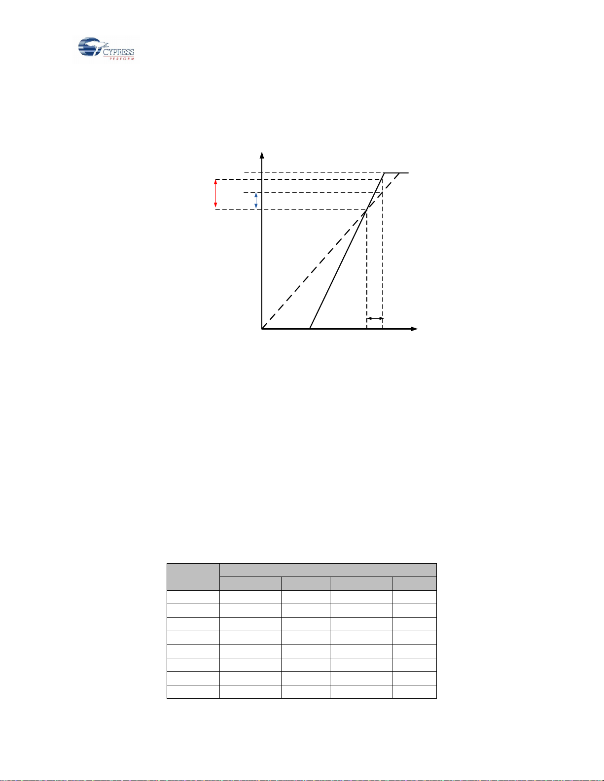
A well-tuned CapSense system reliably discriminates between ON and OFF sensor states. To achieve this level of
performance, the CapSense signal must be significantly larger than the CapSense noise. The CapSense signal is
compared to the CapSense noise by using a quantity called signal-to-noise ratio (SNR). Before discussing the
meaning of SNR for CapSense, it is first necessary to define signal and noise in the context of touch sensing.
4.1.1.1 CapSense Signal
The CapSense signal is the change in the sensor raw count when a finger is placed on the sensor, as demonstrated
in Figure 4-1. The output of the sensor is a digital counter with a value that tracks the sensor capacitance. In this
example, the average level without a finger on the sensor is 5925 counts. When a finger is placed on the sensor, the
average output increases to 6060 counts. Because the CapSense signal tracks the change in counts due to the
finger, Signal = 6060 – 5925 = 135 counts.
Figure 4-1. CapSense Signal and Noise
CY8C20xx7/S CapSense® Design Guide Doc. No. 001-78329 Rev. *E 33
Page 34

CapSense Performance Tuning with User Modules
V
s
V
x
Vref
t
t
R
x
C
x
V
s
V
x
5*Rx*C
x
5*Rx*C
x
Ts
min
>= 10*Rx*C
x
Vref
4.1.1.2 CapSense Noise
CapSense noise is the peak-to-peak variation in sensor response when a finger is not present, as demonstrated in
Figure 4-1. In this example, the output waveform without a finger is bounded by a minimum of 5912 counts and a
maximum of 5938 counts. Because the noise is the difference between the minimum and the maximum values of this
waveform, Noise = 5938 – 5912 = 26 counts.
4.1.1.3 CapSense SNR
CapSense SNR is the simple ratio of signal and noise. Continuing with the example, if the signal is 135 counts and
noise is 26 counts, the SNR is 135:26, which reduces to an SNR of 5.2:1. The minimum recommended SNR for
CapSense is 5:1, which means the signal is five times larger than the noise. Filters are commonly implemented in
firmware to reduce noise. See Software Filtering for more information.
4.1.2 Charge/Discharge Rate
To achieve maximum sensitivity in the tuning process, the sensor capacitor must be fully charged and discharged
during each cycle. The charge/discharge path switches between two states at a rate set by a user module parameter
called Precharge Clock in the CSDPLUS User Module.
The charge/discharge path includes series resistance that slows down the transfer of charge. The rate of change for
this charge transfer is characterized by an RC time constant involving the sensor capacitor (C) and series resistance
(R), as shown in Figure 4-2.
Figure 4-2. Charge/Discharge Waveforms
Set the charge/discharge rate to a level that is compatible with this RC time constant. In general, you should allow a
period of 5 RC for each transition, with two transitions per period (one charge, one discharge). The equations for
minimum time and maximum frequency are:
= 10 × Equation 4-1
=
1
10×
For example, assume the series resistor includes a 560-Ω external resistor and up to 800 Ω of internal resistance,
Equation 4-2
and the sensor capacitance is typical:
RX = 1.4 kΩ
CX= 24 pF
The value of the time constant and maximum front-end switching frequency in this example is:
Ts
CY8C20xx7/S CapSense® Design Guide Doc. No. 001-78329 Rev. *E 34
= 0.34 µs
min
Page 35

CapSense Performance Tuning with User Modules
fs
= 3 MHz
max
4.1.3 Importance of Baseline Update Threshold Verification
Temperature and humidity both cause the average number of counts to drift over time. The baseline is a reference
count level for CapSense measurements that is an important part of compensating for environmental effects. Highlevel decisions, such as Finger Present and Finger Absent states, are based on the reference level established by the
baseline. Because each sensor has unique parasitic capacitance associated with it, each capacitive sensor has its
own baseline.
Baseline tracks the change in counts at a rate set by the Baseline Update Threshold parameter. Make sure to match
the update rate to the intended application. If the update rate is too fast, the baseline will compensate for any
changes introduced by a finger, and the moving finger will not be detected. If the update rate is too slow, relatively
slow environmental changes may be mistaken for fingers. During development, you should verify the Baseline
Update Threshold settings.
4.2 Tuning the CSD/CSDPLUS User Module
Figure 4-3 is a flow chart showing the tuning process for CSD/CSDPLUS UM parameters. CSD/CSDPLUS UM
parameters can be separated into two broad categories: low-level (hardware) parameters and high-level API
parameters. The parameters in these categories affect the behavior of the capacitive sensing system in different
ways. However, there is a complementary relationship between the sensitivity of each sensor as determined by the
hardware parameter settings and many of the high-level parameter settings. You must consider this fact when you
change any hardware parameter to make sure that the corresponding high-level parameters are adjusted
accordingly. Tuning CSD/CSDPLUS User Module parameters should always begin with the hardware parameters.
CY8C20xx7/S CapSense® Design Guide Doc. No. 001-78329 Rev. *E 35
Page 36

CapSense Performance Tuning with User Modules
Measure Cp of sensors
using EP64134
Start
If max Cp < 45 pF set
Idac Range to 4X.
Otherwise set to 8X.
Enable Autocalibration
Set Precharge Source to
PRS
Set Prescaler according
to Table 4-1
Set Resolution according
to Figure 29 and Table 4-2
Set Scanning Speed to
Fast
Set PRS Resolution to
12 bits if scan time >
380 µs according to
Table 4-3. Otherwise set
to 8 bits.
Set Shield
Electrode Out
according to needs
of design
Establish digital
communication interface and
obtain raw counts from each
sensor during finger
activation cycle, for example.
Figure 30
Is SNR from all sensors
> 5:1?
Increase Resolution and/or
experiment with Scanning
Speed until optimal SNR is
obtained
Is SNR from all sensors
> 5:1?
Revise PCB design
according to AN2292 and
AN2318
No
No
Does scan time meet
design requirements?
Yes
Yes
Reduce Resolution or
use faster Scanning
Speed
No
Yes
Set Finger Threshold
to 80% of signal
Set Noise Threshold
to 40% of signal
Set BaselineUpdate
Threshold to double
the Noise Threshold
Set Sensors
Autoreset according to
needs of design
Set Hysteresis to 10%
of signal
Set Debounce
according to needs of
design
Set Negative Noise
Threshold to same
value as Noise
Threshold
Set Low Baseline
Reset to 10
End
Hardware
Parameters
High-Level API
Parameters
Figure 4-3. Tuning the CSD/CSDPLUS User Module
Hardware parameters configure the hardware that the CSD/CSDPLUS method uses to convert the physical
capacitance of each sensor into a digital code. This section describes these parameters and provides guidance about
how each should be tuned based on system characteristics and other parameters.
By default, hardware parameters are global settings that apply to all CapSense sensors in a design. In designs where
total parasitic capacitance of each sensor (CP), sensor sensitivity, or both, vary over a wide range, there may not be
global hardware parameter settings that are suitable for all sensors. In such cases, the SetIdacValue(i),
SetPrescaler(i), and SetScanMode(i) API functions can be used to configure the respective hardware parameters for
each sensor, where (i) is the sensor index before calling the ScanSensor(i) API function.
Table 4-1 and Table 4-3 provide tuning recommendations for several key hardware parameters based on sensor CP.
CP values depend on the characteristics of the PSoC, PCB layout, and proximity of other components in the
assembled product. Because of this, CP must be measured in its original position with the system in its final
assembled state; that is, in the same enclosure and with the same overlay as the system will have in service. The
best way to measure CP is to use the code example "Measuring Absolute Sensor Capacitance with a CY8C20xx6A
CapSense Controller" available in the CapSense Controller Code Examples Design Guide. This project measures the
absolute capacitance of each sensor in a system using the PSoC itself, thus taking into account all factors affecting
CP. See the documentation associated with the code example for instructions on its setup and use.
4.2.1 Recommended C
The recommended C
C
stability over temperature and the capacitor should have a voltage rating not less than 5 V.
MOD
CY8C20xx7/S CapSense® Design Guide Doc. No. 001-78329 Rev. *E 36
Value for CSD/CSDPLUS
MOD
value for a CSD-based design is 2.2 nF. X7R or NPO type capacitors are recommended for
MOD
Page 37

CapSense Performance Tuning with User Modules
CP (pF)
Precharge Source = PRS
Precharge Source = Prescaler
Prescaler
IMO = 24 MHz
Prescaler
IMO = 12 MHz
Prescaler
IMO = 6 MHz
Prescaler
IMO = 24 MHz
Prescaler
IMO = 12 MHz
Prescaler
IMO = 6 MHz
<6 1 Note 1
Note 1
2 1 1
7–11
2 1 Note 1
4 2 1
12–15
2 1 Note 1
4 2 1
16–19
4 2 1 8 4 2 20–22
4 2 1 8 4 2 23–26
4 2 1 8 4 2 27–30
4 2 1 8 4 2 31–34
4 2 1 8 4 2 35–37
8 4 2
16 8 4
4.2.2 I
Range
DAC
For projects where the maximum sensor CP is less than 45 pF, use 4X; otherwise, use 8X.
4.2.3 Autocalibration
Autocalibration should always be set to „Enabled‟ in CY8C20xx7/S CSD/CSDPLUS designs. The ability of the
autocalibration algorithm to successfully set the I
recommended size.
4.2.4 I
DAC
Value
This parameter determines the current output of I
enabled, as recommended, this parameter is overridden and has no effect. When autocalibration is disabled, raising
this parameter lowers the raw count baseline and vice versa. Also, as recommended in IDAC Value in
CSD/CSDPLUS User Module Low-Level Parameters, I
of 2N.
4.2.5 Compensation I
DAC
Value
This parameter determines the current output of the Compensation I
parameter is applicable only for the CSDPLUS UM. When autocalibration is enabled, as recommended, this
parameter is overridden and has no effect. When autocalibration is disabled, raising this parameter lowers the raw
count baseline and vice versa. If auto-calibration is disabled, use the following method to tune compensation I
value.
Initially, tune the raw counts to 85 percent of the maximum raw counts by only using the modulation I
compensation I
tune the modulation I
with a higher value of compensation I
at zero). Then, increase the compensation I
DAC
to get 85 percent of the maximum raw counts. Note down the SNR. Repeat this procedure
DAC
, until maximum SNR is achieved. Note, that a higher compensation I
DAC
value results in higher signal (see Compensation IDAC Value in CSD/CSDPLUS User Module Low-Level Parameters
for more details). Also, note that the best SNR is generally achieved with I
autocalibration also sets the I
DAC
and I
such that I
COMP
relies on the prescaler being set properly and C
DAC
when autocalibration is disabled. When autocalibration is
DAC
value should be chosen such that raw count is 85 percent
DAC
when autocalibration is disabled. This
DAC
to 10 percent of the modulation I
DAC
value = I
DAC
DAC
= I
and raw counts are near 85 percent of 2N.
COMP
MOD
value, and re-
DAC
value. Enabling
COMP.
being the
(keep the
DAC
DAC
DAC
4.2.6 Precharge Source
This parameter selects the sensor switching clock source. The available options are Prescaler, which uses the IMO
through a divider, or PRS, which passes the divided IMO clock through a pseudo random generator, providing a
spread-spectrum clock. PRS provides superior noise immunity and lower noise emissions and is therefore the
recommended default setting for Precharge Source. In some instances, the prescaler precharge source can provide
higher SNR. However, when using copper circuitry, this SNR improvement is usually marginal and rarely justifies
foregoing the benefits of PRS.
4.2.7 Prescaler
Prescaler is the divider applied to the IMO to develop the precharge clock. This is the most critical hardware UM
parameter for properly tuning a CSD design. Prescaler depends on the selected precharge source, IMO, and the CP
of the sensors being scanned. Table 4-1 gives recommended prescaler settings based on these parameters.
Table 4-1. Prescaler Setting Based on Precharge Source, IMO, and CP
CY8C20xx7/S CapSense® Design Guide Doc. No. 001-78329 Rev. *E 37
Page 38

CapSense Performance Tuning with User Modules
CP (pF)
Precharge Source = PRS
Precharge Source = Prescaler
Prescaler
IMO = 24 MHz
Prescaler
IMO = 12 MHz
Prescaler
IMO = 6 MHz
Prescaler
IMO = 24 MHz
Prescaler
IMO = 12 MHz
Prescaler
IMO = 6 MHz
38–41
8 4 2
16 8 4
42–45
8 4 2
16 8 4
46–49
8 4 2
16 8 4
50–52
8 4 2
16 8 4
53–56
8 4 2
16 8 4
57–60
8 4 2
16 8 4
CP (pF)
CF = 0.1 pF
CF = 0.2 pF
CF = 0.4 pF
CF = 0.8 pF
<6
11
10 9 8
7–12
12
11
10 9 13–24
13
12
11
10
25–48
14
13
12
11
>49
15
14
13
12
Note 1 This combination of Precharge Source, Prescaler, and CP is not recommended.
4.2.8 Resolution
Available choices are 9 to 16 bits. Raising the resolution raises sensitivity, SNR, and noise immunity at the expense
of scan time. The maximum raw count (full scale range) for scanning resolution N is 2N-1. Table 4-2 gives
recommended resolution settings based on CP and the finger capacitance CF. CF is the change in capacitance of a
sensor when a finger is placed on the sensor. CF depends on overlay thickness, sensor size, and proximity of the
sensor to other large conductors. Figure 4-4 gives CF values as a function of overlay thickness and circular sensor
diameter.
Figure 4-4. Finger Capacitance (CF) Based on Overlay Thickness and Circular Sensor Diameter
Table 4-2. Resolution Setting Based on Finger Capacitance and CP
4.2.9 Scanning Speed
This parameter controls the integration time for each LSB of the scan result. The choices are Ultra Fast, Fast,
Normal, and Slow. Fast is generally a good starting point. In some, but not all cases, slower scanning speed can yield
CY8C20xx7/S CapSense® Design Guide Doc. No. 001-78329 Rev. *E 38
Page 39

CapSense Performance Tuning with User Modules
Resolution
(bits)
Scanning Speed
Ultra Fast
Fast
Normal
Slow
9
57
78
125
205
10
78
125
205
380
11
125
205
380
720
12
205
380
720
1400
13
380
720
1400
2800
14
720
1400
2800
5600
15
1400
2800
5600
11000
16
2800
5600
11000
22000
Noise
Signal
higher SNR at the expense of longer scan time and more power consumption. Table 4-3 shows the actual scan time
in microseconds for a single sensor based on resolution and scanning speed.
Table 4-3. Scan Time for a Single Sensor in µs Based on Resolution and Scanning Speed
4.2.10 High-Level API Parameters
High-level API parameters determine the behavior of high-level firmware algorithms that discriminate between sensor
activations and noise, and compensate for signal drift caused by environmental conditions. To determine proper
values for these parameters, you must establish a digital communication interface with the system to monitor raw
counts, baseline, and difference counts during a finger activation event for each sensor. This data is stored in arrays
named CSDPLUS_waSnsBaseline[], CSDPLUS_waSnsResult[], and CSDPLUS_waSnsDiff[], respectively. The highlevel API parameter settings are based primarily on ambient noise and finger signal strength, as indicated by this
data. Noise and signal strength depend on EMI environment, PCB layout, overlay thickness, and other physical
characteristics of the system. Therefore, the data used as the basis for setting these parameters must be taken in its
original position with the system in its final assembled state and in the same EMI environment as will exist in use.
Figure 4-5 shows the typical raw counts obtained from a sensor during a finger activation cycle; that is, the sensor is
activated and then deactivated. Labels are superimposed over the data that indicate how noise and signal are to be
calculated based on the raw data. Where appropriate, the high-level parameter descriptions that follow include
information about how to set each parameter based on these noise and signal values. According to CapSense design
best practice, the SNR must be at least 5:1 for robust CapSense system operation. If SNR is less than 5:1, the
hardware parameters must be adjusted, the PCB layout changed according to the guidelines of Getting Started with
CapSense to raise SNR to at least 5:1, or both.
Figure 4-5. Typical Raw Counts from a Sensor During Finger Activation Cycle
CY8C20xx7/S CapSense® Design Guide Doc. No. 001-78329 Rev. *E 39
Page 40

CapSense Performance Tuning with User Modules
4.2.11 Set High-Level Parameters
The following recommendations are a starting place for selecting the optimal parameter settings:
Finger Threshold: Set to 80 percent of raw counts with sensor ON
Noise Threshold: Set to 40 percent of raw counts with sensor OFF
Negative Noise Threshold: Set equal to noise threshold
Baseline Update Threshold: Set to two times noise threshold
Hysteresis: Set to 10 percent of raw counts with sensor ON
Low Baseline Reset: Set to 50
Sensors Autoreset: Based on design requirements
Debounce: Based on design requirements
4.3 Using the SmartSense_EMCPLUS User Module
SmartSense_EMCPLUS allows you to create a CapSense design that requires no tuning, as long as the sensor
parasitic capacitance is in the range from 5 pF to 45 pF with a minimum 0.1-pF finger touch. You can create a
SmartSense_EMCPLUS design by using the SmartSense_EMCPLUS User Module in PSoC Designer 5.1 or higher
versions. This section also shows you how to migrate an existing CSD CapSense design to
SmartSense_EMC_PLUS.
4.3.1 Guidelines for SmartSense_EMC_PLUS
Follow these guidelines when using the SmartSense_EMCPLUS User Module in an application:
SmartSense_EMCPLUS requires that the capacitive user interface design follows the layout and system design
best practices documented in the Design Considerations section.
All of the CSD/CSDPLUS UM parameters (such as I
resolution) are determined at runtime by the SmartSense_EMCPLUS User Module. You should not use APIs that
modify these CSD parameters in firmware, unless you know exactly what effect it has in your design.
To migrate an existing design from CSD/CSDPLUS to SmartSense_EMC_PLUS:
Ensure that all APIs that set or modify the CSD/CSDPLUS parameters are first removed from the program.
Ensure that the parasitic capacitance of all CapSense sensors in the design is between 5 pF and 45 pF over
environmental and PCB production process variations.
Make sure recommended C
the C
port pin selected in the user module wizard.
MOD
capacitor (X7R, 2.2-nF, and voltage rating more than 5 V) is connected to
MOD
value, prescaler period, clock divider, scan speed, and
DAC
4.3.2 Understanding the Difference
The differences between the SmartSense_EMCPLUS User Module and the standard CSD/CSDPLUS User Module
are:
The SmartSense_EMCPLUS User Module supports the same APIs that a standard CSD/CSDPLUS User
Module supports. Thus, no change is required in placing, configuring, starting, or calling other APIs except the
User Module instance name.
There is no need to set any User Module parameters for tuning, as all the parameters related to tuning are
automatically set at runtime by the SmartSense_EMCPLUS User Module.
The C
than 5 V is recommended in all CapSense applications.
The SmartSense_EMCPLUS algorithm maintains the signal SNR of each sensor between 5:1 and 11:1 to ensure
robust CapSense operation while maximizing performance.
The scanning time of the SmartSense_EMCPLUS User Module is restricted by the algorithm to be between
410 µs and 2.8 ms per sensor in 24-MHz operating mode, based on the parasitic capacitance of the sensor.
CY8C20xx7/S CapSense® Design Guide Doc. No. 001-78329 Rev. *E 40
capacitor value is restricted to 2.2 nF. Use of an X7R or NPO capacitor with a voltage rating higher
MOD
Page 41

CapSense Performance Tuning with User Modules
4.3.3 Recommended C
The recommended C
are recommended for C
value for a SmartSense_EMC_PLUS-based design is 2.2 nF. X7R or NPO type capacitors
MOD
stability over temperature. The capacitor should have voltage rating not less than 5 V.
MOD
Value for SmartSense_EMC_PLUS
MOD
4.3.4 SmartSense_EMCPLUS User Module Parameters
Only four parameters must be set for this user module. These are:
Sensors Autoreset
Debounce
Modulator Capacitor Pin
Sensitivity Level
4.3.4.1 Sensors Autoreset
This parameter determines whether the baseline is updated at all times or only when the signal difference is below
the noise threshold. When set to Enabled, the baseline is updated constantly. This setting limits the maximum time
that a sensor may remain ON (typically it is 5 to 10 seconds), but it prevents the sensors from permanently turning
ON when the raw count suddenly rises without anything touching the sensor because of any failure condition of the
system.
4.3.4.2 Debounce
The Debounce parameter adds a debounce counter to the sensor‟s active transition. For the sensor to be declared as
active from inactive state, a finger touch signal should be present on the sensor for debounce number of consecutive
scans. This parameter affects all of the sensors similarly.
4.3.4.3 Modulator Capacitor Pin
This parameter selects the pin to which the 2.2 nF/X7R/voltage rating more than 5 V C
The available pins are P0[1] and P0[3].
Note An external 2.2-nF capacitor is mandatory for SmartSense_EMCPLUS to work correctly.
capacitor is connected.
MOD
4.3.4.4 Sensitivity Level
Sensitivity is used to increase or decrease strength of signal from a sensor. A lower value for sensitivity (0.1 pF)
leads to a stronger signal from the sensor. Designs with thicker overlays require stronger signals from sensors for
proper implementation. The available options for sensitivity selection are High (0.1 pF), Medium High (0.2 pF),
Medium Low (0.3 pF), and Low (0.4 pF).
To produce a stronger signal from a sensor (high sensitivity), the SmartSense_EMCPLUS UM must use more time
for sensor scanning. This means that setting 0.1-pF (High) sensitivity for a sensor will consume more scan time
compared to the sensor that has the sensitivity level set to 0.2 pF (Medium High).
Tuning best practice is to find the highest sensitivity value for the sensor to produce the required 5:1 SNR. You may
start the tuning with the highest sensitivity value (0.4 pF) and reduce the value as required to meet the 5:1 SNR
4.3.5 SmartSense_EMCPLUS User Module Specific Guidelines
All guidelines applicable to the SmartSense_EMC UM apply to the SmartSense_EMCPLUS UM. For general
guidelines about CapSense design and SmartSense_EMC_PLUS-based design, see the Getting Started with CapSense
design guide. This section documents a few important aspects of the SmartSense_EMCPLUS UM.
4.3.5.1 Sensor Scan Time, Response Time, and Memory Utilization
When a sensor is implemented using the SmartSense_EMCPLUS UM, the scan time of a sensor, response time of
the sensor, and RAM memory usage depends on the immunity mode selected in the user module.
With immunity mode Medium, sensor scan time is two times higher than a sensor with immunity mode Low. With
immunity mode High, the scan time of a sensor is three times higher than the scan time of a sensor with
immunity mode Low.
Increase in scan time proportionally increases the response time of a sensor. With immunity mode Medium,
response time is two times higher than that of a sensor with immunity mode Low. Similarly, response time of a
sensor with immunity mode High is three times higher than that of a sensor with immunity mode Low.
CY8C20xx7/S CapSense® Design Guide Doc. No. 001-78329 Rev. *E 41
Page 42

CapSense Performance Tuning with User Modules
Sensitivity = 0.2 pF
Sensitivity = 0.3 pF
Sensitivity = 0.4 pF
CP (pF)
ST (µs)
CP (pF)
ST (µs)
CP (pF)
ST (µs)
8 to 10
340
8 to 17
340
8 to 10
170
10 to 23
680
17 to 35
680
10 to 23
340
23 to 41
1360
35 to 41
1360
23 to 41
680
41 to 45
2730
41 to 45
2730
41 to 45
1360
Sensitivity = 0.2 pF
Sensitivity = 0.3 pF
Sensitivity = 0.4 pF
CP (pF)
ST (µs)
CP (pF)
ST (µs)
CP (pF)
ST (µs)
8 to 10
680
8 to 17
680
8 to 10
340
To implement a robust electromagnetic compliant algorithm, the SmartSense_EMCPLUS UM uses RAM
memory. As a result, the highest immunity mode (High) needs approximately three times the RAM memory used
in immunity mode Low. Immunity mode Medium uses only about two times more RAM memory than that of
immunity mode Low.
4.3.5.2 IMO Tolerance and Time Critical Task
IMO tolerance for SmartSense_EMC-enabled parts is +5 percent and –20 percent.
When implementing time-critical algorithms and logic, you must consider IMO tolerance to make sure that the
firmware logic or algorithm does not break.
If a project uses interrupts, you should consider IMO tolerance while analyzing interrupt latency, ISR execution
time, and so on.
Every timing analysis that depends on the IMO (for example, a timer clocked by IMO, delay created using loop in
firmware, and API execution time) must consider the IMO tolerance to ensure robust application firmware.
4.3.5.3 I2C Operating Speed
I2C interface operation frequency is limited to a maximum of 80 percent of the actual operating frequency of the user
module in the SmartSense_EMC-enabled parts. This limitation is caused by the 20-percent IMO tolerance.
This means, when clock speed of 400 kHz is selected in the I2C user module, the I2C interface can be operated
to maximum of 320 kHz. Similarly, operating frequency is limited to a maximum of 80 kHz and 40 kHz when
100-kHz and 50-kHz clock modes, respectively, are selected in the I2C user module.
While using the I2C slave interface, the master clock should operate within the reduced specification mentioned
earlier. Not doing this will lead to data corruption, I2C bus conjunction, or inconsistent behavior from the I2C user
module.
Using the I2C master module impacts only the throughput of the interface.
When using I2CSBUF user module, it is strongly recommended use auto-nack mode while CPU accessing the 32-
byte dedicated buffer and when device put into sleep or deep sleep modes. See the I2CSBUF user module datasheet
details information.
4.3.6 Scan Time of a CapSense Sensor
To maintain the consistent finger response sensitivity over a wide range of parasitic capacitance, the
SmartSense_EMCPLUS User Module automatically determines the hardware parameters of the user module. As a
result, sensor scan time does not remain constant. For a design in mass production, it could vary based on the
parasitic capacitance variation of the PCB.
The total scan time of a sensor is decided by four factors. They are parasitic capacitance of sensor, IMO frequency,
CPU operating frequency, and sensitivity level of the SmartSense_EMCPLUS User Module.
Scan time of a sensor can be found using Equation 4-3 and the following tables.
= + () Equation 4-3
The following tables show the sampling time value with various IMO and sensitivity levels.
Table 4-4. Sampling Time for a Sensor with IMO = 24 MHz
Table 4-5. Sampling Time for a Sensor with IMO = 12 MHz
CY8C20xx7/S CapSense® Design Guide Doc. No. 001-78329 Rev. *E 42
Page 43

CapSense Performance Tuning with User Modules
10 to 23
1360
17 to 35
1360
10 to 23
680
23 to 41
2730
35 to 41
2730
23 to 41
1360
41 to 45
5460
41 to 45
5460
41 to 45
2730
Sensitivity = 0.2 pF
Sensitivity = 0.3 pF
Sensitivity = 0.4 pF
CP (pF)
ST (µs)
CP (pF)
ST (µs)
CP (pF)
ST (µs)
8 to 11
680
8 to 10
680
8 to 11
680
11 to 23
1360
10 to 17
1360
11 to 23
1360
23 to 42
2730
17 to 35
2730
23 to 41
2730
42 to 45
5460
35 to 41
5460
41 to 45
5460
41 to 45
10920
CPU CLK
Processing Time (PT) in µs
24
71
12
142 6 284
3
568
Table 4-6. Sampling Time for a Sensor with IMO = 6 MHz
Table 4-7 shows the value for processing time with various CPU frequencies.
Table 4-7. Processing Time for a Sensor
For example, if a CapSense system is designed with a 24-MHz IMO frequency, a 6-MHz CPU clock (IMO/4), and a
SmartSense_EMCPLUS sensitivity level of 0.3 pF, the scan time of the sensor that has parasitic capacitance around
15 pF can be calculated from the previous tables using Equation 4-1.
Sampling time for the previously mentioned configuration (24 MHz of IMO and 0.3 pF of sensitivity) is chosen from
Table 4-4; it is 680 µs. Processing time for the previously mentioned configuration (CPU clock of 6 MHz) Is chosen
from Table 4-7; it is 284 µs.
Thus, the total scan time in this configuration is 680 + 284 = 964 µs. Scan time for more than one sensor is the sum
of the scan time of each sensor.
4.3.7 SmartSense_EMCPLUS Response Time
Consider the following application with standard CSD along with typical CapSense scanning firmware.
Three CapSense sensors with parasitic capacitance of sensor between 5 pF and 10 pF
IMO of 12 MHz and CPU clock of 12 MHz
Sensor sensitivity level of 0.4 pF
Debounce = 3
According to the previous tables, scanning of each sensor requires 482 µs and three sensors have a scan time of
1.45 ms. The following firmware example requires 1 ms for additional firmware execution; thus, the loop execution
time will be 2.45 ms.
while (1)
{
SmartSense_EMC_PLUS_ScanAllSensors();
SmartSense_EMCPLUS _UpdateAllBaselines();
if(SmartSense_EMCPLUS _bIsAnySensorActive() )
{
//1ms firmware routines
}
}
CY8C20xx7/S CapSense® Design Guide Doc. No. 001-78329 Rev. *E 43
Page 44

CapSense Performance Tuning with User Modules
This means that, when a CapSense sensor is activated, firmware produces the sensor ON status within 7.35 ms (the
sensor should be active for debounce number of consecutive scans). This is often referred to as the response time of
a CapSense system.
If the scan time varies with respect to the parasitic capacitance to maintain consistent, what is the impact on
response time if the parasitic capacitance of the sensor changes because of the process variation? Response time
may be increased (slow response) in this case. This can have a negative impact on sensor performance. Guidelines
to build a robust firmware design are provided in the next section.
4.3.8 Method to Ensure Minimum SNR Using the SmartSense_EMCPLUS UM
SmartSense_EMCPLUS is an advanced electromagnetic compliance design of a CSD-based SmartSense user
module that does not require a tedious tuning process. However, there are two simple steps to ensure robustness of
the design while using the SmartSense_EMCPLUS UM.
1. Set up a real-time monitoring tool to monitor the CapSense user module parameters to measure sensor signals.
The sensor raw count (SmartSense_EMCPLUS_waSnsResult), sensor normalized signal
(SmartSense_EMCPLUS_baSnsSignal), and sensor finger threshold
(SmartSense_EMCPLUS_baBtnFThreshold) must be observed during the tuning process. Do not use the LCD
or any other numerical displays to monitor data because they are slow and do not allow visualizing the data
dynamics. Recommended data monitoring tools are multi-chart or the I2C USB Bridge Control Panel.
2. Set the sensitivity level to 0.4 pF (Low), and calculate the SNR. Figure 4-6 shows a typical raw count graph with
a finger touch. According to CapSense best practices, SNR for a robust design should be greater than 5:1. If
measured SNR is more than 10:1, reduce sensitivity level value to the next possible step until SNR is more than
5:1 and less than 10:1.
Figure 4-6. Raw Count Graph for a Typical Sensor with a Finger Touch
3. If you are using the automatic finger threshold feature in the design, the process is complete after the previous
step. If you are using the flexible finger threshold feature, you should also set individual finger thresholds for
each sensor to complete the process. To set finger threshold, monitor sensor signal
(SmartSense_EMCPLUS_baSnsSignal) and set finger threshold value to roughly 80 percent of the sensor signal
value when the sensor is touched. This completes the process. Figure 4-7 shows a typical sensor signal and
finger threshold value.
CY8C20xx7/S CapSense® Design Guide Doc. No. 001-78329 Rev. *E 44
Page 45

CapSense Performance Tuning with User Modules
Figure 4-7. Sensor Signal for a Typical Sensor with a Finger Touch
4.3.9 Firmware Design Guidelines
The response time of the CapSense sensors may change due to the increased parasitic capacitance of the sensor. It
is also important to watch the loop execution time (see the following example code), which may also increase. When
the parasitic capacitance of all sensors is less than 10 pF, the firmware routine is executed at a rate of 2.45 ms. This
rate will change if the sensor scan time is increased because of the increase in the parasitic capacitance of the
sensor based on the process variation.
The following is example code for toggling a port pin based on the main loop execution time.
while (1)
{
SmartSense_EMC_PLUS_ScanAllSensors();
SmartSense_EMC_PLUS_UpdateAllBaselines();
if(SmartSense_EMC_PLUS_bIsAnySensorActive() )
{
//1ms firmware routines
}
PRT0DR_Shadow ^= 0x01;
PRT0DR = PRT0DR_Shadow;
}
The period of the signal on the Port_0[1] pin is 4.9 ms (the period is twice the loop time as the port pin is toggled). If
the parasitic capacitance of one sensor is increased to approximately 15 pF, the scan time will change to 1.78 ms;
thus, the period of the signal on Port_0[1] will be 5.6 ms.
If the parasitic capacitance of the sensor is close to the boundary of the SmartSense_EMCPLUS capacitance banks
(for example, 9 pF, which is very close to the 10-pF boundary), SmartSense_EMCPLUS may choose a neighboring
scan time in an application because of process variation. Because of this, different production parts of the same
design can have two different main loop execution times and response times.
Based on the above discussion, firmware should not rely on the scan time of the sensor for implementing other
features (for example, software PWM, software delay, and so on). Programs implementing a watchdog timer (WDT)
should consider this fact while setting the WDT expiration time
A simple firmware implementation example to get a consistent main loop execution time using the Timer16 User
Module follows.
// Main program
BYTE bTimerTicks = 0;
#pragma interrupt_handler myTimer_ISR_Handler;
void myTimer_ISR_Handler( void );
CY8C20xx7/S CapSense® Design Guide Doc. No. 001-78329 Rev. *E 45
Page 46

CapSense Performance Tuning with User Modules
void main()
{
M8C_EnableGInt;
SmartSense_EMC_PLUS_Start();
SmartSense_EMC_PLUS_ScanAllSensors();
SmartSense_EMC_PLUS_SetDefaultFingerThresholds() ;
Timer16_EnableInt();
Timer16_SetPeriod (TIMEOUT_10MS) ;
Timer16_Start();
while( 1 )
{
/* Scan all 3 sensors and update
Baseline */
SmartSense_EMC_PLUS_ScanAllSensors();
SmartSense_EMC_PLUS_UpdateAllBaselines();
/* Wait till timer expires or
sleep here */
while (bTimerTicks != 1) ;
bTimerTicks = 0 ;
if(CSDAUTO_bIsAnySensorActive() )
{
//1ms firmware routines
}
// Toggle Port_0[1]
PRT0DR_Shadow ^= 0x01 ;
PRT0DR = PRT0DR_Shadow ;
}
}
// Timer16 ISR program
void myTimer_ISR_Handler(void)
{
bTimerTicks++;
}
In the previous example, the program waits for the timer to expire even if the sensor scanning is complete. The timer
period should be chosen based on the worst-case main loop execution time. This is the sum of the worst-case scan
times of the individual CapSense sensors. If the parasitic capacitance of the sensor is close to the boundary of the
SmartSense_EMCPLUS capacitance bank, choose a higher scan time (using Table 4-5) for the calculation.
The SmartSense_EMCPLUS UM enables you to easily implement the capacitive touch-sensing user interface into a
system. It removes the difficulties of the tuning process and helps to increase the yield in production against
manufacturing process variations of the PCB and other variations. Therefore, the preferred option is to migrate the
existing CSD-based CapSense designs to SmartSense_EMCPLUS and to use SmartSense_EMCPLUS for new
designs.
The main loop execution time and scan time of SmartSense_EMCPLUS vary based on the process variations.
Though it does not affect the performance of CapSense in any way, the firmware developer should consider this
when implementing CapSense PLUS applications with SmartSense_EMCPLUS Auto-Tuning technology.
CY8C20xx7/S CapSense® Design Guide Doc. No. 001-78329 Rev. *E 46
Page 47
CapSense Performance Tuning with User Modules
System Requirements
I2CSBUF
EzI2Cs
I2CHW
I2Cm
Wake on I2C slave address match
Yes
Yes
No
N/A
Master requires clock stretch
No
Yes
Yes
N/A
I2C data buffer size
1-32 bytes
1-255 bytes
1-255 bytes
N/A
I2C master
No
No
No
Yes
Package
Pin Compatibility to CY8C20xx6A/AS
16-SOIC
New package offering with CY8C20xx7/S
16-QFN
Pin to pin compatible
24-QFN
One pin - Pin 23 is Vss in CY8C20xx7/S while it is an I/O in CY8C20xx6A/AS
32-QFN
Two pins - Pin 28 is I/O and Pin 29 is Vss in CY8C20xx7/S; in CY8C20xx6A/AS, Pin 28 is Vss and Pin
29 is an I/O
30-WLCSP
Pin to pin compatible
48-QFN
Two pins - Pins 36 and 45 are NC while in CY8C20xx6A/AS both are I/O
4.4 Design Migration from CY8C20xx6A/AS to CY8C20xx7/S
The CY8C20xx7/S family of CapSense controllers provides superior noise immunity based on QuiteZoneTM
technology and improved sensitivity of 0.1 pF with a 5:1 SNR. This section summarizes key points to migrate an
existing CY8C20xx6A/AS design.
4.4.1 Discontinued Support/User Modules
The USB interface has been discontinued in the CY8C20xx7/S family.
On-chip debug (OCD) support has been discontinued for the CY8C20xx7/S family.
CSA and CSA_EMC user modules are not supported in the CY8C20xx7/S family.
4.4.2 Improvement and New Features
CSD-based improved CapSense sensing engine to provide an improved sensitivity of 0.1 pF.
New improved I2C slave interface (I2CSBUF User Module) with dedicated 32-byte buffer eliminating clock
stretching by the slave.
Improved I2C interface also supports wakeup interrupt from I2C slave address match event.
Use Table 4-8 to select the correct I2C User Module for your design.
Table 4-8. I2C Features
4.4.3 Pin Compatibility
Table 4-9. Pin Compatibility
CY8C20xx7/S CapSense® Design Guide Doc. No. 001-78329 Rev. *E 47
Page 48

5. Design Considerations
When designing capacitive touch-sense technology into your application, it is crucial to keep in mind that the
Material
r
Breakdown Voltage
(V/mm)
Minimum Overlay Thickness
at 12 kV (mm)
Air
1.0
1200–2800
10
Wood – dry
1.2–2.5
3900
3
Glass – common
7.6–8.0
7900
1.5
Glass – Borosilicate (Pyrex®))
6.0
13,000
0.9
PMMA Plastic (Plexiglas®)
2.8
13,000
0.9
ABS
2.4–4.1
16,000
0.8
Polycarbonate (Lexan®)
2.9–3.0
16,000
0.8
Formica
4.6–4.9
18,000
0.7
FR-4
4.8
28,000
0.4
PET Film – (Mylar®)
3.2
280,000
0.04
Polymide film – (Kapton®)
2.9-3.9
290,000
0.04
CapSense device exists within a larger framework. Careful attention to every level of detail from PCB layout to user
interface to end-use operating environment will lead to robust and reliable system performance. For more in-depth
information, see Getting Started with CapSense.
5.1 Overlay Selection
In CapSense Fundamentals, Equation 4-1 was presented for finger capacitance
0
=
Where:
ε
= Free space permittivity
0
ε
= Dielectric constant of overlay
r
A = Area of finger and sensor pad overlap (mm2)
D = Overlay thickness (mm)
To increase CapSense signal strength, choose an overlay material with a higher dielectric constant, decrease the
overlay thickness, and increase the button diameter.
Table 5-1. Overlay Material Dielectric Strength
Conductive material cannot be used as an overlay because it interferes with the electric field pattern. For this reason,
do not use paints containing metal particles in the overlay.
An adhesive is typically used to bond the overlay to the CapSense PCB. A transparent acrylic adhesive film from
3M™ called 200MP is qualified for use in CapSense applications. This special adhesive is dispensed from paperbacked tape rolls (3M product numbers 467MP and 468MP).
CY8C20xx7/S CapSense® Design Guide Doc. No. 001-78329 Rev. *E 48
Page 49

Design Considerations
ESD Protection Device
Input
Capacitance
Leakage
Current
Contact
Discharge
Maximum Limit
Air Discharge
Maximum Limit
Manufacturer
Part Number
Littelfuse
SP723
5 pF
2 nA
8 kV
15 kV
Vishay
VBUS05L1-DD1
0.3 pF
0.1 µA <
±15 kV
±16 kV
NXP
NUP1301
0.75 pF
30 nA
8 kV
15 kV
5.2 ESD Protection
Robust ESD tolerance is a natural byproduct of thoughtful system design. By considering how contact discharge will
occur in your product, particularly in your user interface, it is possible to withstand an 18-kV discharge event without
incurring any damage to the CapSense controller.
CapSense controller pins can withstand a direct 2-kV event. In most cases, the overlay material provides sufficient
ESD protection for the controller pins. Table 5-1 lists the thickness of various overlay materials required to protect the
CapSense sensors from a 12-kV discharge, as specified in IEC 61000-4-2. If the overlay material does not provide
sufficient protection, ESD countermeasures should be applied in the following order: Prevent, Redirect, Clamp.
5.2.1 Prevent
Make sure that all paths on the touch surface have a breakdown voltage greater than potential high-voltage contacts.
Also, design your system to maintain an appropriate distance between the CapSense controller and possible sources
of ESD. If it is not possible to maintain adequate distance, place a protective layer of a high breakdown voltage
material between the ESD source and the CapSense controller. One layer of 5-mil-thick Kapton® tape will withstand
18 kV.
5.2.2 Redirect
If your product is densely packed, it may not be possible to prevent the discharge event. In this case, you can protect
the CapSense controller by controlling where the discharge occurs. A standard practice is to place a guard ring on
the perimeter of the circuit board that is connected to chassis ground. As recommended in PCB Layout Guidelines,
providing a hatched ground plane around the button or slider sensor can redirect the ESD event away from the
sensor and CapSense controller.
5.2.3 Clamp
Because CapSense sensors are purposely placed close to the touch surface, it may not be practical to redirect the
discharge path. In this case, including series resistors or special-purpose ESD protection devices may be
appropriate.
The recommended series resistance value is 560 Ω.
A more effective method is to provide special-purpose ESD protection devices on the vulnerable traces. ESD
protection devices for CapSense need to be low capacitance. Table 5-2 lists devices recommended for use with
CapSense controllers.
Table 5-2. Low-Capacitance ESD Protection Devices Recommended for CapSense
5.3 Electromagnetic Compatibility (EMC) Considerations
5.3.1 Radiated Interference
Radiated electrical energy can influence system measurements and potentially influence the operation of the
processor core. The interference enters the PSoC chip at the PCB level, through CapSense sensor traces and any
other digital or analog inputs. Layout guidelines for minimizing the effects of RF interference include:
Ground Plane: Provide a ground plane on the PCB.
Series Resistor: Place series resistors within 10 mm of the CapSense controller pins.
The recommended series resistance for CapSense input lines is 560 Ω.
The recommended series resistance for communication lines such as I2C and SPI is 330 Ω.
Trace Length: Minimize trace length whenever possible.
CY8C20xx7/S CapSense® Design Guide Doc. No. 001-78329 Rev. *E 49
Page 50

Design Considerations
Type
Description
Application
Average
Finite impulse response filter (no feedback) with
equally weighted coefficients
Periodic noise from power supplies
IIR
Infinite impulse response filter (feedback) with a
step response similar to an RC filter
High frequency white noise (1/f noise)
Median
Nonlinear filter that computes median input value
from a buffer of size N
Noise spikes from motors and switching power supplies
Jitter
Nonlinear filter that limits current input based on
previous input
Noise from thick overlay (SNR < 5:1), especially useful for
slider centroid data
Event-Based
Nonlinear filter that causes a predefined
response to a pattern observed in the sensor
data
Commonly used during non-touch events to block CapSense
data transmission.
Rule-Based
Nonlinear filter that causes a predefined
response to a pattern observed in the sensor
data
Commonly used during normal operation of the touch surface
to respond to special scenarios such as accidental
multibutton selection
Current Loop Area: Minimize the return path for current. Hatched ground instead of solid fill should be provided
within 1 cm of the sensors and traces to reduce the impact of parasitic capacitance.
RF Source Location: Partition systems with noise sources such as LCD inverters and switched-mode power
supplies (SMPS) to keep them separated from CapSense inputs. Shielding the power supply is another common
technique for preventing interference.
5.3.2 Radiated Emissions
Selecting a low frequency for the switched-capacitor clock helps to reduce radiated emissions from the CapSense
sensor. This clock is controlled in firmware using the prescaler option. Increasing the prescaler value decreases the
frequency of the switching clock.
5.3.3 Conducted Immunity and Emissions
Noise entering a system through interconnections with other systems is referred to as conducted noise. These
interconnections include power and communication lines. Because CapSense controllers are low-power devices,
conducted emissions must be avoided. The following guidelines will help reduce conducted emission and immunity:
Use decoupling capacitors as recommended by the datasheet.
Add a bidirectional filter on the input to the system power supply. This is effective for both conducted emissions
and immunity. A pi-filter can prevent power supply noise from effecting sensitive parts, while also preventing the
switching noise of the part from coupling back onto the power planes.
If the CapSense controller PCB is connected to the power supply by a cable, minimize the cable length and
consider using a shielded cable.
Place a ferrite bead around power supply or communication lines to filter out high-frequency noise.
5.4 Software Filtering
Using software filters is one of the techniques for dealing with high levels of system noise. Table 5-3 lists the types of
filters that are useful for CapSense.
Table 5-3. Table of CapSense Filters
Table 5-4 details the RAM and flash requirements for different software filters. The amount of flash required for each
filter type depends on the performance of the compiler. The requirements listed here are for both the ImageCraft
compiler and the ImageCraft Pro compiler.
CY8C20xx7/S CapSense® Design Guide Doc. No. 001-78329 Rev. *E 50
Page 51

Design Considerations
Filter Type
Filter
Order
RAM
(Bytes per sensor)
Flash (Bytes)
ImageCraft Compiler
Flash (Bytes)
ImageCraft Pro Compiler
Average
2–8 6 675
665
IIR
1 2 429
412
2 6 767
622
Median
3 6 516
450
5
10
516
450
Jitter filter on raw counts
N/A 2 277
250
Jitter filter on slider centroid
N/A 2 131
109
Table 5-4. RAM and Flash Requirements
5.5 Power Consumption
5.5.1 System Design Recommendations
For many designs, minimizing power consumption is an important goal. There are several ways to reduce the power
consumption of your CapSense capacitive touch-sensing system.
Set GPIO drive mode for low power
Turnoff the high-power blocks
Optimize CPU speed for low power
Operate at a lower VDD
In addition to these suggestions, applying the sleep-scan method can be very effective.
5.5.2 Sleep-Scan Method
In typical applications, the CapSense controller does not need to always be in the active state. The device can be put
into the sleep state to stop the CPU and the major blocks of the device. Current consumed by the device in sleep
state is much lower than the active current.
The average current consumed by the device over a long period can be calculated by using the following equation.
=
×
+(
)
×
Equation 5-1
The average power consumed by the device can be calculated as follows:
= ×
Equation 5-2
5.5.3 Response Time versus Power Consumption
As illustrated in Equation 5-2, the average power consumption can be reduced by decreasing I
decreased by increasing sleep time. Increasing sleep time to a very high value will lead to poor CapSense button
response time. As a result, the sleep time must be based on system requirements.
In any application, if both power consumption and response time are important parameters to be considered, an
optimized method can be used that incorporates both continuous-scan and sleep-scan modes. In this method, the
device spends most of its time in sleep-scan mode where it scans the sensors and goes to sleep periodically, as
explained in the previous section, thereby consuming less power. When a user touches a sensor to operate the
system, the device jumps to continuous-scan mode where the sensors are scanned continuously without invoking
sleep, thereby giving very good response time. The device remains in continuous-scan mode for a specified timeout
period. If the user does not operate any sensor within this timeout period, the device jumps back to the sleep-scan
mode.
or VDD. I
AVE
may be
AVE
CY8C20xx7/S CapSense® Design Guide Doc. No. 001-78329 Rev. *E 51
Page 52

Design Considerations
5.5.4 Measuring Average Power Consumption
The following instructions describe how to determine average power consumption when using the sleep-scan
method:
1. Build a project that scans all of the sensors without going to sleep (continuous-scan mode). Include a pin-toggle
feature in the code before scanning the sensors. Toggling the state of the output pin serves as a time marker that
can be tracked with an oscilloscope.
2. Download the project to the CapSense device and measure the current consumption. Assign the measured
current to I
3. Get the sleep current information from the datasheet and assign it to I
4. Monitor the toggling output pin in the oscilloscope and measure the time period between two toggles. This gives
the active time. Assign this value to t
5. Apply sleep-scan to the project. The period of the sleep-scan cycle, T, is set by selecting the sleep timer
frequency in the global resources window as shown in Figure 5-1.
6. Subtract active time from the sleep-scan cycle period to get the sleep time. T
7. Calculate the average current using Equation 5-1.
8. Calculate average power consumption using Equation 5-2.
ACT
.
.
SLP
.
ACT
SLP
= T – t
ACT
.
Figure 5-1. Global Resources Window
5.6 Pin Assignments
An effective method to reduce interaction between CapSense sensor traces and communication and non-CapSense
traces is to isolate each by port assignment. Figure 5-2 shows a basic version of this isolation for a QFN package.
Because each function is isolated, the CapSense controller is oriented such that there is no crossing of
communication, LED, and sensing traces.
CY8C20xx7/S CapSense® Design Guide Doc. No. 001-78329 Rev. *E 52
Page 53

Design Considerations
Recommended for LED Drive
Recommended for CapSense Sensors and CMOD
P0.1, P2.5, P2.3, P2.1, P4.1, P3.7, P3.5,
P3.3, P3.1, P1.7, P1.5, P1.3, P1.1
P1.0, P1.2, P1.4, P1.6, P3.0, P3.2, P3.4, P3.6, P4.0,
P4.2, P2.0, P2.2, P2.4, P0.0, P0.2, P0.4, P0.6, P0.3
Figure 5-2. Recommended Port Isolation for Communication, CapSense, and LEDs
All GPIOs of the CapSense controller are capable of implementing the CapSense sensor and drive LEDs. However, if
the GPIOs LED drive and CapSense sensors are implemented in the same project, it is recommended to use GPIO
according to Table 5-5 for best performance. If a design is implementing only CapSense sensors or only LED drive,
the restrictions mentioned in Table 5-5 are not applicable.
Table 5-5. Recommended GPIOs for LED Drive and CapSense Sensors
The architecture of the CapSense controller imposes a restriction on current budget for even and odd port pin
numbers. An odd pin can be any port pin having an odd number as pin number. For a CapSense controller, if the
current budget of odd port pin is 100 mA, the total current drawn though all odd port pins should not exceed 100 mA.
In addition to the total current budget limitation, there is also a maximum current limitation for each port pin that is
defined in the CapSense controller datasheet.
All CapSense controllers provide high-current sink and source capable port pins. When using high-current sink or
source from port pins, it is recommended to use the ports that are closest to device ground pin to minimize the noise.
5.7 GPIO Load Transient
When GPIOs sink a large current (>10 mA) to the ground of the chip by driving port pins to strong-low, noise will be
introduced into the CapSense system. The instantaneous change in the amount of the current flow to ground through
the GPIOs is referred as GPIO load transient. The noise introduced into the CapSense system due to the GPIO load
transient is called GPIO load transient noise, as shown in Figure 5-3. This section shows you how to reduce the
GPIO load transient noise using hardware techniques, and compensate the noise using firmware techniques.
CY8C20xx7/S CapSense® Design Guide Doc. No. 001-78329 Rev. *E 53
Page 54

Design Considerations
GPIO Load Transient
Noise
LED is ON
LED is OFF
GPIO PAD
CapSense GND
GPIO GND
VSS
R1
R2
R3
GPIO PIN
CS Sensor
AMUX
Figure 5-3. GPIO Load Transient Noise in a CapSense System
When current is sunk through a GPIO pin, the voltage at CapSense ground (GPIO PAD) will not be zero because of
the non-zero bond-wire resistance, R3. Because of the non-zero ground potential, the sensor will not be completely
discharged when LED is sinking current; this will cause an increase in the sensor raw count.
Figure 5-4. Ground Structure in CY8C20xx7/S
Note: R1, R2, and R3 are bond wire resistances.
For a robust CapSense design, the worst-case GPIO transient noise should be less than 30 percent of the finger
touch signal. The worst-case noise appears in the CapSense system when the GPIO state is changed from a nocurrent-flow state (for example, all LEDs OFF) to a maximum current flow state (for example, all LEDs ON).
The GPIO load transient noise increases with the sensor scan resolution. CapSense sensors with a high parasitic
capacitance or proximity sensors require higher sensor-scan resolution to achieve an SNR greater than 5:1. In such
systems, the effect of GPIO load transient is more pronounced. In some cases, the noise due to GPIO load transient
might be higher than the signal due to finger touch and cause sensor false-triggers. The following section shows how
to reduce GPIO load transient noise.
5.7.1 Hardware Guidelines to Reduce GPIO Load Transient Noise
Reduce Sensor CP
The sensor CP determines the sensor scan resolution parameter. The larger the C
the higher will be the
P,
resolution parameter required to achieve an SNR greater than 5:1. Setting a high-resolution parameter causes
CY8C20xx7/S CapSense® Design Guide Doc. No. 001-78329 Rev. *E 54
Page 55

Design Considerations
the amplitude of the GPIO load transient-noise to increase. Therefore, it is recommended to minimize the sensor
CP by following the layout guidelines mentioned in the Getting Started with CapSense design guide.
Reduce LED sink current
The GPIO load transient noise is directly proportional to the LED sink current. It is recommended to keep the
LED sink current within the limits as specified in the device datasheet. If the GPIO has to sink a current, which is
more than the maximum value specified in datasheet, use an external transistor or a driver IC.
Select appropriate pins for LED
All CapSense controllers provide high-current sink- and source-capable port pins. When using high-current sink
or source from port pins, you should use the ports recommended in Table 5-5.
5.7.2 Firmware Guidelines to Compensate GPIO Load Transient Noise
To prevent sensor false triggers due to GPIO load transients, the sensor baseline can be updated using rule-based
algorithms. One of the methods to compensate the baseline is explained here.
Figure 5-5 shows a condition in which false triggers is seen due to GPIO load transient.
1. At instant 1, there is no finger on the sensor and the LED is in the OFF condition.
2. At instant 2, a finger is on the sensor and the shift in raw count is greater than the finger threshold.
3. Because the shift in raw count is greater than the finger threshold, the LED is turned ON at instant 3.
4. When the LED is turned ON, because of GPIO load-transient, the raw count further shifts.
5. At instant 4, even if the finger is removed, the raw count will not return to initial value because of the shift in the
raw count due to the GPIO load-transient. If this shift is greater than the finger threshold, the LED will remain ON
permanently indicating a sensor false-trigger.
To prevent the sensor and the LED from remaining in ON condition permanently, the sensor baseline should be
compensated, which is explained in the below steps.
CY8C20xx7/S CapSense® Design Guide Doc. No. 001-78329 Rev. *E 55
Page 56

Design Considerations
No Touch
Touch
No Touch
Finger Threshold
Shift Due to
Finger Touch
Shift Due to GPIO Load
Transient
Rawcount Stuck due to
GPIO Load Transient
LED OFF LED ON
Sensor Status
Baseline
Rawcount
1
2
3
4
Figure 5-5. CapSense Sensor Variables when Baseline is Not Compensated
Figure 5-6 shows a condition in which false triggers is eliminated by compensating the sensor baseline.
1. At instant 1, there is no finger on the sensor and the LED is in the OFF condition.
2. At instant 2, a finger is on the sensor and the shift in raw count (difference count) is greater than the finger
threshold.
3. Because the shift in difference count is greater than the finger threshold, the LED is turned ON at instant 3.
4. When the LED is turned ON, the noise due to GPIO load transient is calculated. That is, noise = raw count (when
LED is ON) – raw count (when LED is OFF)
This noise count due to GPIO load transient is added to the baseline, and as a result, when the finger is
removed, the difference count value will be zero and the LED will be turned OFF.
5. After the LED is turned off, the raw count will return to the initial value and the baseline is reset due to the low-
baseline reset algorithm.
CY8C20xx7/S CapSense® Design Guide Doc. No. 001-78329 Rev. *E 56
Page 57

Design Considerations
No Touch
Touch
No Touch
Finger Threshold
Shift Due to
Finger Touch
Shift Due to GPIO Load
Transient
Difference Count is Zero Due to
Baseline Compensation
LED OFF
LED ON
Sensor Status
Baseline
Rawcount
1
2
3
4
LED OFF
Baseline
Compensated
Rawcount Returns to Initial Value
After LED is Turned OFF
Baseline is reset due to Low
Baseline Reset Algorithm
5
Figure 5-6. CapSense Sensor Variables when Baseline is Compensated
5.8 PCB Layout Guidelines
Detailed PCB layout guidelines are available in Getting Started with CapSense.
CY8C20xx7/S CapSense® Design Guide Doc. No. 001-78329 Rev. *E 57
Page 58

6. Liquid-Tolerant Design Considerations
Some CapSense capacitive touch-sensing applications require reliable operation in the presence of water or other
PCB
Shield Electrode
Guard Sensor
Sensor Pads
liquids such as ketchup and blood. White goods, automotive applications, and industrial applications are examples of
systems that must perform in environments that include water, ice, humidity changes, or any other liquids. For such
applications, shield electrodes and guard sensors can provide robust touch sensing.
6.1 Shield Electrode and Guard Sensor
Figure 6-1. PCB Layout with Shield Electrode and Guard Sensor
6.1.1 Shield
Shield electrodes protect CapSense button sensors from detecting false touches caused by water drops or liquid
spills. When water drops or any other liquid spills are present on the overlay surface, the coupling between the shield
electrode and sensor pad is increased by CLD, as shown in Figure 6-2.
CY8C20xx7/S CapSense® Design Guide Doc. No. 001-78329 Rev. *E 58
Page 59

Liquid-Tolerant Design Considerations
Figure 6-2. Capacitance Measurement with Liquid Drop
CLD = Capacitance between the liquid drop and shield electrode
The purpose of the shield electrode is to set up an electric field around the touch sensors that helps attenuate the
effects of water. The shield electrode works by mirroring the voltage of the touch sensor on the shield.
Follow these guidelines to ensure proper shield operation:
Schematic
Layout
Firmware development
6.1.1.1 Schematic
Select the proper pin to drive the shield electrode out signal. The following pins should be used to drive the shield
electrode out signal.
Port pins: P0[0], P1[2], P0[2], P2[2], or P2[4]
6.1.1.2 Layout
Follow the layout guidelines given in Getting Started with CapSense.
6.1.1.3 Firmware Development
There is a shield drive GUI, as shown in Figure 6-3, to minimize firmware development.
Figure 6-3. Driven Shield GUI (Shield Inactive)
Step 1: Enable the CapSense Shield Signal from the GUI.
Click on “Ebuf0”, which is the EnableShieldDriver switch, as shown in Figure 6-4; the “Disable” option is selected by
default. Select CapsenseShieldSignal to enable the shield driver.
CY8C20xx7/S CapSense® Design Guide Doc. No. 001-78329 Rev. *E 59
Page 60

Liquid-Tolerant Design Considerations
Shield Buffer
Output Port Pin
Buf 0
Port_2_4
Buf 1
Port_2_2
Buf 2
Port_0_2
Buf 3
Port_0_0
Buf 4
Port_1_2
Figure 6-4. Enabling CapsenseShieldSignal from GUI
Step 2: Route the shield electrode out to the shield pin.
There are five possible shield drive buffers, labeled Buf 0 through Buf 4; their mapping is shown in the following table.
The shield drive buffers are OFF by default; select the desired shield drive buffer. Figure 6-5 shows the enabling of
Buf 0 such that the shield signal is driven out on Port_2_4.
Figure 6-5. Schematic View of Output Select
Step 3: Choose polarity of the shield signal.
There are two polarity choices, see Figure 6-8:
Normal Mode (default): Shield driver signal in phase with sensor scan signal
Reverse Polarity: Shield driver signal 180° out of phase with sensor scan signal
Normal Mode shows the best performance in liquid-tolerant designs.
CY8C20xx7/S CapSense® Design Guide Doc. No. 001-78329 Rev. *E 60
Page 61

Liquid-Tolerant Design Considerations
PCB
Shield Electrode
Guard Sensor
Sensor Pads
6.1.2 Guard Sensor
Figure 6-6. Schematic View of Polarity Select
Figure 6-7. PCB with Shield and Guard Sensor
A guard sensor is a copper trace, as shown in Figure 6-9, that surrounds all the sensors on the PCB, which is used to
detect the presence of a continuous water stream or a large liquid spill. When a water stream or a large liquid spill is
present on the sensing surface, a large-capacitance CST is added to the system, as shown in Figure 6-8. This
capacitance may be several times larger than CLD. Because of this, the effect of the shield electrode is completely
masked and the raw counts measured by the sensor will be the same as or even higher than a finger touch. In this
situation, a guard sensor will help; when it detects a water stream, it will block the other sensors from triggering.
CY8C20xx7/S CapSense® Design Guide Doc. No. 001-78329 Rev. *E 61
Page 62

Liquid-Tolerant Design Considerations
Figure 6-8. Capacitance Measurement with Large Liquid Spills or Water Stream
C
C
C
- Capacitance between the water stream/liquid spill and shield electrode
LD
- Capacitance between the water stream/liquid spill and the system ground
ST
- Capacitance between the water stream/liquid spill and the guard sensor
WG
The guard sensor should be implemented in firmware. One CapSense pin and a counter (hardware/software) are
required to implement the guard sensor.
When a water stream or a large liquid spill is present on the board, the guard sensor detects this event and disables
the touch sensor processing logic. Additional guard sensor "dead" time prevents unlocking the sensor prematurely.
When the liquid is gone, the guard counter suppresses touch processing for a short time (guard sensor counter). This
eliminates false touch detection from any water/liquid that remains on the board.
Figure 6-9 is a flow chart that shows how the guard sensor should be implemented in firmware.
CY8C20xx7/S CapSense® Design Guide Doc. No. 001-78329 Rev. *E 62
Page 63

Liquid-Tolerant Design Considerations
Start of main function
End of main function
Initialize CapSense block and other blocks
Scan all sensors including Guard sensor
Update baseline of all sensors
Is Guard Sensor ON? Turn off all the sensors
Guard sensor
counter elapsed?
Report sensor status normally
Yes
No
No
Yes
Figure 6-9. Flow Chart to Implement the Guard Sensor
6.2 Design Recommendations
The following system-level and PCB layout recommendations apply to CapSense systems that will be exposed to
liquids or humid environments:
Shield-electrode copper-hatch recommendations:
Top layer – 7-mil trace and 45-mil grid (15-percent fill)
Bottom layer – 7-mil trace and 70-mil grid (10-percent fill)
The shield electrode between buttons should be at least 10 mm wide
Place sensor surface vertically or at an angle to the horizontal so that water drops or liquid spills naturally move
off the sensors and large liquid drops do not accumulate.
Use liquid-repellent and nonabsorbent overlay material. This minimizes liquid streaks and films on the device
panel. This is especially important if the liquid is highly conductive, such as seawater.
You must use a guard sensor in situations where the application may be subjected to continuous water streams
or large liquid spills. A guard sensor is not required if the device will be subjected only to rain, mist, or humid
conditions.
CY8C20xx7/S CapSense® Design Guide Doc. No. 001-78329 Rev. *E 63
Page 64

7. Proximity Sensing Design Considerations
Proximity sensors detect the presence of a hand or other conductive object before it makes contact with the
Proximity Sensor
capacitive touch surface. Imagine a hand stretched out to operate a car audio system in the dark. Proximity detection
enables the system to light up with the approach of a finger. For example, the buttons of an audio system will glow
with its backlight LEDs when the user's hand is near.
7.1 Types of Proximity Sensors
7.1.1 Button
A button with large CP and small difference counts can work as a proximity sensor. The sensitivity of a proximity
sensor implemented as a button is much higher than a regular capacitive touch-sensing button.
7.1.2 Wire
A single length of wire works well as a proximity sensor. Because detecting a hand relies on the capacitance change
from electric field changes, any stray capacitance or objects affecting the electrical field around the wire will affect the
range of the proximity sensor. Using a wire sensor is not an optimal solution for mass production because of
manufacturing cost and complexity.
7.1.3 PCB Trace
A long PCB trace can form a proximity sensor. The trace can be a straight line, or it can surround the perimeter of a
system‟s user interface, as shown in Figure 7-1. This method is appropriate for mass production, but it is not as
sensitive as a wire sensor.
Figure 7-1. Proximity Sensor Using PCB Trace
7.1.4 Sensor Ganging
Another way to implement a proximity sensor is to gang sensors together. This is accomplished by combining
multiple sensors into one large sensor, using firmware to connect the sensors from the internal analog multiplexer
bus in PSoC Designer. Be careful not to exceed the CP limit of your design when using this method.
CY8C20xx7/S CapSense® Design Guide Doc. No. 001-78329 Rev. *E 64
Page 65

Proximity Sensing Design Considerations
7.2 Design Recommendations
Using a shield electrode effectively extends the detection distance of the proximity sensor. This is particularly
helpful when the proximity sensor must operate in the presence of metal.
A wire sensor increases the beneficial effect of the shield electrode because it can be located farther from the
shield electrode.
Avoid large, solid ground-fill areas inside the proximity sensor, because this decreases the sensitivity.
Slower scan speeds provide increased sensitivity at all distances. For a proximity sensor, the scanning speed
should be very slow.
CY8C20xx7/S CapSense® Design Guide Doc. No. 001-78329 Rev. *E 65
Page 66

8. Low-Power Design Considerations
Power consumption is an important aspect of microcontroller designs. Among the several techniques to reduce the
average current used by the CapSense controller, sleep mode is the most popular. The CapSense controller uses
sleep mode when it is not required to perform any function, similar to a cell phone backlight dimming after an idle
period. This is done to reduce the average current consumed by the device, a necessity of all battery applications.
The CapSense controller enters sleep mode by writing a „1‟ to the SLEEP bit within the CPU_SCR0 register (Bit 3).
This is accomplished by calling the M8C_Sleep macro.
While in sleep mode:
the central CPU is stopped
the IMO is disabled
the bandgap voltage reference is powered down
the flash memory model is disabled
The only circuits left in operation are the supply voltage monitor and the 32-kHz internal oscillator.
Power-saving techniques other than the standard sleep mode are:
I2C sleep mode (see section Entry into I2C Sleep Mode)
Disable CapSense (PSoC) analog block references
Disable CT and SC blocks
Disable CapSense (PSoC) analog output buffers
Set drive modes to analog HI-Z
Sleep mode has negative effects for a design. If not used carefully, it can cause an unpredictable operation. The
PSoC must be correctly awakened from sleep when necessary and the user must be aware that the device is
sleeping to allow extra processing.
8.1 Additional Power Saving Techniques
All of the power-saving techniques, with the exception of sleep mode, is application-based. Some of them produce
undesirable results. Each technique is discussed in detail in the following sections.
8.1.1 Set Drive Modes to Analog HI-Z
The state of the CapSense controller drive modes can affect power consumption. You can change the drive modes
only on pins that do not cause adverse effects to the system. The change must occur in a sequence that does not
produce line glitches. This sequence depends on the current drive mode of the pin and the state of the port data
register. With the CapSense controller drive mode structure, the pin must temporarily be in either Resistive Pull-up or
Resistive Pull-down drive mode when switching between HI-Z or Strong drive modes. The temporary drive mode is
the opposite of the previous value on the pin. Therefore, if the pin was driven high, then the temporary drive mode
must be Resistive Pull-down. This ensures that the drive mode of the pin is not resistive, which eliminates any
possible glitch.
The drive modes are set manually in software, before going to sleep. Three registers, PRTxDM0, PRTxDM1, and
PRTxDM2, control the drive modes. One bit per register is assigned to a pin. Therefore, to change the drive mode of
a single pin, three register writes are needed. However, this is convenient because an entire port is changed by the
same three register writes. The correct pit pattern for Analog HI-Z is 110b. Use the following code to set port zero to
Analog HI-Z from Strong, by first going to Resistive Pull-down.
CY8C20xx7/S CapSense® Design Guide Doc. No. 001-78329 Rev. *E 66
Page 67

Low-Power Design Considerations
PRT0DM0 = 0x00; // low bits
PRT0DM1 = 0xff; // med bits
PRT0DM2 = 0xff; //high bits
8.1.2 Putting it All Together
The following code is a sample of a typical sleep preparation sequence for a 28-pin part. In this sequence, interrupts
are disabled, the analog circuitry is turned off, all drive modes are set to Analog HI-Z, and interrupts are re-enabled.
void PSoC_Sleep(void)
{
M8C_DisableGInt;
PRT0DM0 = 0x00; // port 0 drives
PRT0DM1 = 0xff;
PRT0DM2 = 0xff;
PRT1DM0 = 0x00; // port 1 drives
PRT1DM1 = 0xff;
PRT1DM2 = 0xff;
PRT2DM0 = 0x00; // port 2 drives
PRT2DM1 = 0xff;
PRT2DM2 = 0xff;
M8C_EnableGInt;
M8C_Sleep;
}
8.1.3 Recommended I2C Slave Implementation in Sleep Mode
When I2C is used in sleep mode, certain implementation guidelines must be followed to keep the I2C bus from locking
or corrupted transactions from occurring.
8.1.3.1 Entry into I2C Sleep Mode
In general, the I2C slave must be put into a FORCE_NACK mode before entering the sleep mode. These steps need
to be followed to enter the sleep mode correctly:
Select the mode of operation (clock stretch or NACK during sleep to wakeup) through CLK_STRETCH_EN bit of
the I2C_BP_EZ_CFG register
Set the FORCE_NACK bit of the I2C_XCFG register
Poll status bit I2C_XSTAT.READY_TO_NACK for logic „1‟
Set the I2C_ON bit in the SLP_CFG2 register
Call the M8C_Sleep function (this sets the SLEEP bit (Bit 3) within the CPU_SCR0 register)
Note: Data retention during sleep and deep sleep modes in the 32-byte I2C buffer is guaranteed only if power to the
I2C block is enabled by asserting I2C_ON bit in the SLP_CFG2 register.
8.1.4 Sleep Mode Complications
The CapSense controller can exit sleep either from a reset or through an interrupt. The CapSense controller has
three types of resets: External Reset, Watchdog Reset, and Power-On Reset. Any of these resets takes the
CapSense controller out of sleep mode. After the reset deasserts, the CapSense controller begins executing code
starting at Boot.asm. Available interrupts to wake the CapSense controller are: Sleep Timer, Low-Voltage Monitor,
GPIO, Analog Column, and Asynchronous. Sleep mode complications arise when using interrupts to wake the
CapSense controller or attempting digital communication while asleep. These considerations are discussed in detail
in the following sections.
8.1.5 Pending Interrupts
If an interrupt is pending, enabled, and scheduled to occur after a write to the SLEEP bit in the CPU_SCR0 register,
the system will not go to sleep. The instruction still executes, but the CapSense controller does not set the SLEEP bit.
Instead, the interrupt is serviced, which effectively causes the CapSense controller to ignore the sleep instruction. To
avoid this, interrupts should be globally disabled while sleep preparation occurs and then re-enabled just before
writing the SLEEP bit.
CY8C20xx7/S CapSense® Design Guide Doc. No. 001-78329 Rev. *E 67
Page 68

Low-Power Design Considerations
8.1.6 Global Interrupt Enable
The Global Interrupt Enable register (CPU_F) need not be enabled to wake the CapSense controller from interrupts.
The only requirement to wake up from sleep by an interrupt is to use the correct interrupt mask within the INT_MSKx
registers, as in the following example. If global interrupts are disabled, the ISR that wakes the CapSense controller is
not executed but the CapSense controller still exits sleep mode.
In this case, you must manually clear the pending interrupt or enable global interrupts to allow the ISR to be serviced.
Interrupts are cleared within the INT_CLRx registers.
//Set Mask for GPIO Interrupts
M8C_EnableIntMask(INT_MSK0, INT_MSK0_GPIO)
// Clear Pending GPIO Interrupt
INT_CLR0 &= 0x20;
8.2 Post Wakeup Execution Sequence
If the CapSense controller is awakened through a reset, execution starts at the beginning of the boot code. If the
CapSense controller is awakened by an interrupt service routine, the first instruction to execute is the one
immediately following the sleep instruction. This is because the instruction immediately following the sleep instruction
is pre-fetched before the CapSense controller is fully asleep. Therefore, if global interrupts are disabled, the
instruction execution will continue where it left off before sleep was initiated.
8.2.1 PLL Mode Enabled
If PLL mode is enabled, the CPU frequency must be reduced to the minimum of 3 MHz before going to sleep. This is
because the PLL always overshoots as it attempts to relock after the CapSense controller wakes up and is reenabled. Additionally, you should wait 10 ms after wakeup before normal CPU operation begins to ensure proper
execution. This implies that, to use sleep mode and the PLL, the software must be able to execute at 3 MHz. A
simple write to the OSC_CR0 register can reduce CPU speed. However, this register just sets a divider of SYSCLK,
which means that the CPU speed will vary between part families with different SYSCLKs. Typically, SYSCLK is
24 MHz
OSC_CR0 &= 0xf8; // CPU = 3 Mhz IMO = 24 Mhz
8.2.2 Execution of Global Interrupt Enable
Avoid interrupts on the instruction boundary of writing the SLEEP bit. This can cause all firmware preparations for
going to sleep to be bypassed, if a sleep command is executed on a return from interrupt (reti) instruction. To prevent
this, interrupts are temporarily disabled before sleep preparations and then re-enabled before going to sleep.
Because of the timing of the Global Interrupt instruction, an interrupt cannot occur during the next instruction, which in
this case is setting the SLEEP bit.
8.2.3 Recommended I2C Slave Implementation in Sleep Mode
When I2C is used in sleep mode, certain implementation guidelines must be followed to keep the I2C bus from locking
or corrupted transactions from occurring.
8.2.3.1 Wakeup from I2C Sleep Mode using HW Address Match
To enable the wakeup through I2C, set the HW Addr EN bit so that the I2C slave block wakes the system if and only if
the address matches. The I2C block responds to the transactions on the I2C bus when the system is in sleep mode
but when the system is in sleep mode, the system clock shuts down.
Therefore, if the I2C block must respond to the transactions on the I2C bus, then the block does not have system
clock to work on. As a result, the incoming SCL clock is used as the clock for the block to respond to the transactions
on the bus.
When the address matches, the behavior depends on the CLK_STRETCH_EN setting. If this bit is set high, SCL is
pulled low until the IMO is operational. If this bit is set low, the slave NACKS all I2C transactions addressed to it until
the CPU wakes up and sets the ACK bit. When clock stretch mode is disabled, after a wakeup IRQ, any other start
condition will not be recognized by the device until the IMO is operational. All transactions in this duration will receive
a NACK. Figure 8-1 depicts the wakeup sequence through I2C.
CY8C20xx7/S CapSense® Design Guide Doc. No. 001-78329 Rev. *E 68
Page 69

Low-Power Design Considerations
Figure 8-1. Wakeup Sequence
8.2.4 Sleep Timer
The CapSense controller offers a sleep timer and a Sleep Timer User Module. These are used while the CapSense
controller is asleep and both perform similar functions. The actual sleep timer runs off the internal low-speed
oscillator, which is never turned off. At selectable intervals of 1 Hz, 8 Hz, 64 Hz, and 512 Hz, the timer generates an
interrupt. It is often useful to periodically wake the CapSense controller up to do some processing or check for
activity. An example of this is to periodically wake up to scan a sensor. The Sleep Timer User Module uses the sleep
timer to generate some additional functionality. This functionality includes a background tick counter to generate
periodic interrupts, a delay function for program loops, a settable down counter, and a loop governor to control loop
time. A simple block diagram for this functionality is shown in Figure 8-2. .
Figure 8-2. Sleep Timer User Module Block Diagram
CY8C20xx7/S CapSense® Design Guide Doc. No. 001-78329 Rev. *E 69
Page 70

9. Resources
9.1 Website
Visit Cypress‟s CapSense Controllers website to access all of the reference material discussed in this section.
Find a variety of technical resources for the CapSense CY8C20xx7/S family of devices on the CY8C20xx7/S web
page.
9.2 Datasheet
The datasheet for the CapSense CY8C20xx7/S family of devices are available at www.cypress.com.
CY8C20xx7/S Datasheet
9.3 Technical Reference Manual
Cypress created the following technical reference manual to give quick and easy access to information on the
CapSense controller functionality, including top-level architectural diagrams along with register and timing diagrams.
CY8C20xx7/S Technical Reference Manual (TRM)
CY8C20xx7/S CapSense® Design Guide Doc. No. 001-78329 Rev. *E 70
Page 71

Resources
9.4 Development Kits
9.4.1 CY8C20xx7/S QuietZone Starter Kit
The CY8C20xx7/S QuietZone Starter Kit shown as Figure 9-1 is a 0.75-inch squared PCB based on the
CY8C20247S 16-pin QFN package.
Figure 9-1. CY8C20xx7/S QuietZone Starter Kit
The CY8C20xx7/S QuietZone Starter Kit hardware has the following features:
Twelve capacitive sensing inputs
One 5-pin header (HD1) for easy connection to MiniProg1/3
One driven shield output
Two LEDs for visual feedback
The kit is available from our module partner ArtaFlex at the following link: www.artaflexmodules.com/quietzone
9.4.2 Universal CapSense Controller Kit
The CY8C20xx7/S family does not have on-chip debug (OCD) capability; if a debug platform is needed, then the
CY8C20xx6A Universal CapSense Controller Kit is available. The Universal CapSense Controller Kits feature
predefined control circuitry and plug-in hardware to make prototyping and debugging easy. Programming and I2C-toUSB Bridge hardware are included for tuning and data acquisition.
CY3280-20xx6A Universal CapSense Controller
9.4.3 Universal CapSense Module Boards
9.4.3.1 Simple Button Module Board
The CY3280-BSM Simple Button Module consists of 10 CapSense buttons and 10 LEDs. This module connects to
any CY3280 Universal CapSense Controller Board
9.4.3.2 Matrix Button Module Board
The CY3280-BMM Matrix Button Module consists of eight LEDs and eight CapSense sensors organized in a 4×4
matrix format to form 16 physical buttons. This module connects to any CY3280 Universal CapSense Controller
Board.
CY8C20xx7/S CapSense® Design Guide Doc. No. 001-78329 Rev. *E 71
Page 72

Resources
9.5 Sample Board Files
Cypress offers sample schematic and board files, which can be used as a reference to quickly complete your PCB
design process.
Button design with I2C header on CY8C20xx7/S
Button and slider design with I2C header on CY8C20xx7/S
Note The board files (schematic, layout, and Gerber files) will be placed in the landing page of this document.
Figure 9-2 and Figure 9-3 show the board schematics.
The following schematic is designed to support:
Two CapSense sensors. The sensors are assigned to pins P2[5] and P1[5] of the CY8C20237-24SXI device.
Two GPIOs connected to pins P0[7] and P0[4] of CY8C20237-24SXI to drive LEDs D1 and D2.
Shield electrode is connected to pin P1[2]to drive shield plane.
Programming lines and I2C SDA/SCL signals of CY8C20237-24SXI connected to header J1.
Figure 9-2. Button Design with I2C Header on CY8C20237 - Board Schematic
The following schematic is designed to support the following:
Four CapSense sensors. The sensors are assigned to pins P0[1], P2[1], P3[3], and P1[7] of the CY8C20437-
24LQXI device.
Guard sensor is connected to pin P4[3] of the CY8C20437-24LQXI device.
Four GPIO pins P1[4], P1[6], P3[0], and P3[2] CY8C20437-24LQXI to drive LEDs D1, D2, D3, and D4.
Programming of CY8C20437-24LQXI by way of the programming header J2.
9-V DC input can be connected to header J7.
CY8C20xx7/S CapSense® Design Guide Doc. No. 001-78329 Rev. *E 72
Page 73

Resources
Figure 9-3. Liquid-Tolerant Button Design with I2C Header on CY8C20437
CY8C20xx7/S CapSense® Design Guide Doc. No. 001-78329 Rev. *E 73
Page 74

Resources
9.6 PSoC Programmer
PSoC Programmer is a flexible, integrated programming application for programming PSoC devices. It can be used
with PSoC Designer and PSoC Creator™ to program any design onto a PSoC device.
PSoC Programmer includes a hardware layer with APIs to design specific applications using the programmers and
bridge devices. The PSoC Programmer hardware layer is fully detailed in the COM guide documentation as well as
example code across the following languages: C#, C, Perl, and Python.
9.7 CapSense Data Viewing Tools
Many times during CapSense design, you will want to monitor relevant CapSense data (raw counts, baseline,
difference counts, and so on) for tuning and debugging purposes. Application note AN2397 – CapSense Data
Viewing Tools gives information to help you identify and use the right tools for CapSense data viewing and logging.
9.8 PSoC Designer
Cypress offers an exclusive integrated design environment (IDE), PSoC Designer. With PSoC Designer, you can
configure analog and digital blocks, develop firmware, and tune your design. Applications are developed in a dragand-drop design environment using a library of fully characterized analog and digital functions, including CapSense.
PSoC Designer comes with a built-in C compiler and an embedded programmer. A pro compiler is available for
complex designs.
9.9 Code Examples
Cypress offers a large collection of code examples to get your design up and running fast.
CapSense Controller Code Examples Design Guide
9.10 Design Support
Cypress has a variety of design support channels to ensure the success of your CapSense solutions.
Knowledge Base Articles – Refer to technical articles by product family or perform a search on various
CapSense topics.
CapSense Application Notes – Refer to a wide variety of application notes built on information presented in this
document.
White Papers – Learn about advanced capacitive-touch interface topics.
Cypress Developer Community – Connect with the Cypress technical community and exchange information.
CapSense Product Selector Guide – See the complete product offering of Cypress‟s CapSense product line.
Video Library – Quickly get up to speed with tutorial videos
Quality & Reliability – Cypress is committed to complete customer satisfaction. At our Quality website you can
find reliability and product qualification reports.
Technical Support – World class technical support is available online.
CY8C20xx7/S CapSense® Design Guide Doc. No. 001-78329 Rev. *E 74
Page 75

Revision History
Document Title: AN78329 - CY8C20xx7/S CapSense® Design Guide
Document Number: 001-78329
Revision
Issue Date
Origin of
Change
Description of Change
**
05/09/2012
DST
New Design Guide
*A
06/28/2012
UDYG
Edits made to 8.1.3.1 Entry into I2C Sleep Mode
*B
09/06/2012
ZINE
Updated links to external documents
*C
11/27/2012
DST
Page 17: Added link to QuietZone Starter Kit external web
Updated Section 3.4.2.4
Pg 40: Added table 4-8
Updated Section 6.1.1.1
*D
01/21/2015
PRIA/DCHE
Added sections Switched-Capacitor Input and Sigma Delta Converter
Added section GPIO Load Transient
Renamed Chapter 6 to -Tolerant Design Considerations
Updated template
Changed the document title to CY8C20xx7/S CapSense® Design Guide – AN78329
*E
03/24/2015
DCHE
Added section 2.2.4, 2.2.1
Updated Figure 4-3, Figure 2-1 and Figure 4-2
Added footnote in Page 8
Added information on driven shield in section 1.3
Updated recommended values in section 4.2.11
Added hyperlinks in section 9.4.2 and 9.4.3
Document Revision History
CY8C20xx7/S CapSense® Design Guide Doc. No. 001-78329 Rev. *E 75
 Loading...