

CY8C20534, CY8C20434
CY8C20334, CY8C20234
PSoC® Mixed-Signal Array
Features
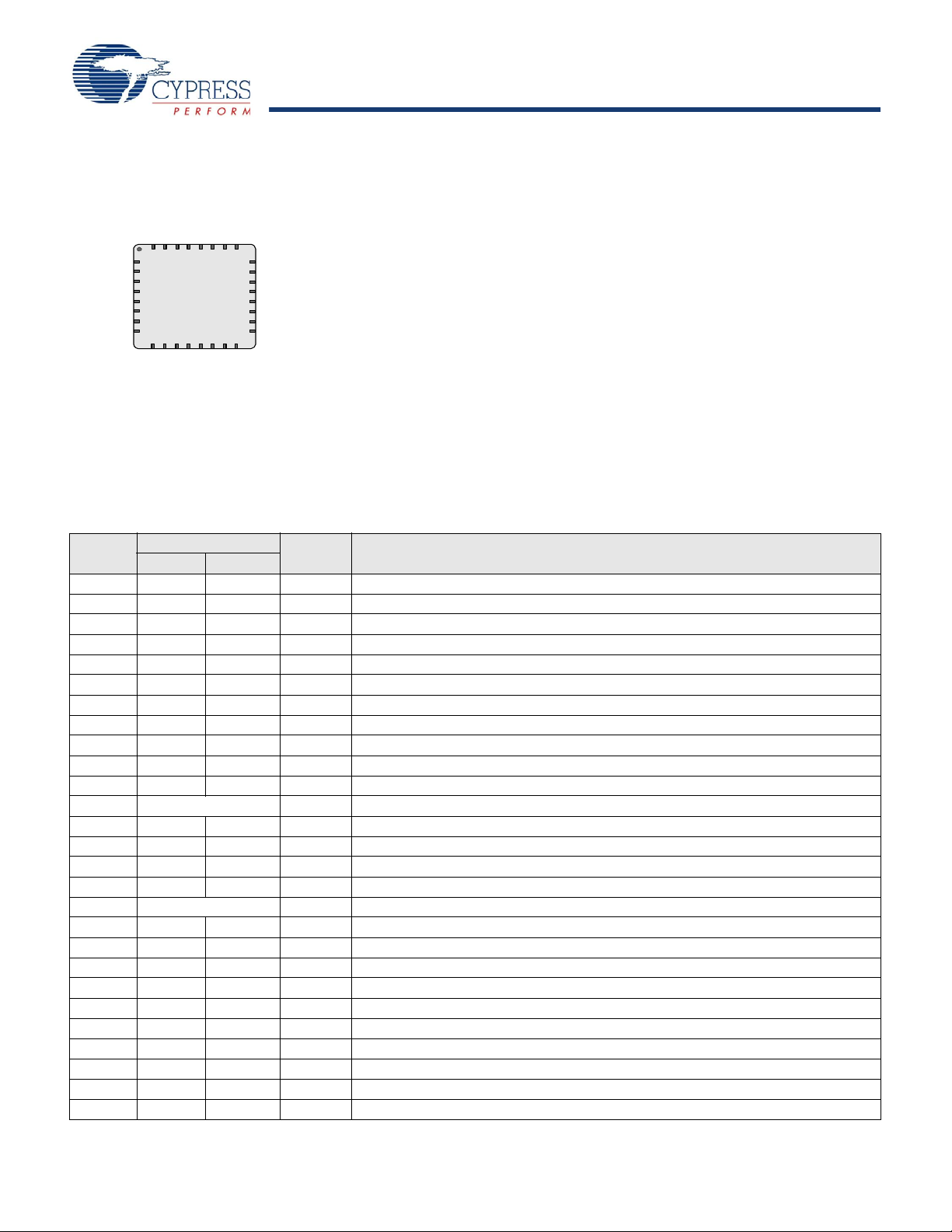
Logic Block Diagram
SRAM
512 Bytes
System Bus
Interrupt
Controller
6/12 MHz Internal Main Oscillator
Global Analog Interconnect
PSoC
CORE
CPU Cor e
(M8C)
SROM Flash 8K
SYSTEM RESOURCES
ANALOG
SYSTEM
Analog
Ref.
I2C Slave/SPI
Master-Slave
POR and LVD
System Re sets
Port 1 Port 0
Sleep and
Watchdog
Analog
Mux
Port 3 Port 2
CapSense
Block
Config LDO
■ Low Power CapSense Block
❐ Configurable Capacitive Sensing Elements
❐ Supports Combination of CapSense Buttons, Sliders, Touch-
pads, and Proximity Sensors
■ Powerful Harvard Architecture Processor
❐ M8C Processor Speeds Running up to 12 MHz
❐ Low Power at High Speed
❐ 2.4V to 5.25V Operating Voltage
❐ Industrial Temperature Range: -40°C to +85°C
■ Flexible On-Chip Memory
❐ 8K Flash Program Storage
50,000 Erase/Write Cycles
❐ 512 Bytes SRAM Data Storage
❐ Partial Flash Updates
❐ Flexible Protection Modes
❐ Interrupt Controller
❐ In-System Serial Programming (ISSP)
■ Complete Development Tools
❐ Free Development Tool (PSoC Designer™)
❐ Full Featured, In-Circuit Emulator, and
Programmer
❐ Full Speed Emulation
❐ Complex Breakpoint Structure
❐ 128K Trace Memory
■ Precision, Programmable Clocking
❐ Internal ±5.0% 6/12 MHz Main Oscillator
❐ Internal Low Speed Oscillator at 32 kHz for W atchdog and Sl eep
■ Programmable Pin Configurations
❐ Pull Up, High Z, Open Drain, and CMOS Drive Modes on All
GPIO
❐ Up to 28 Analog Inputs on GPIO
❐ Configurable Inputs on All GPIO
❐ Selectable, Regulated Digital IO on Po rt 1
• 3.0V, 20 mA Total Port 1 Source Current
• 5 mA Strong Drive Mode on Port 1 Versatile Analog Mux
❐ Common Internal Analog Bus
❐ Simultaneous Connection of IO Combinations
❐ Comparator Noise Immunity
❐ Low Dropout Voltage Regulator for the Analog Array
■ Additional System Resources
❐ Configurable Communication Speeds
•I2C: Selectable to 50 kHz, 100 kHz, or 400 kHz
• SPI: Configurable between 46.9 kHz and 3 MHz
2
❐ I
C™ Slave
❐ SPI Master and SPI Slave
❐ Watchdog and Sleep Timers
❐ Internal Voltage Reference
❐ Integrated Supervisory Circuit
Cypress Semiconductor Corporation • 198 Champion Court • San Jose, CA 95134-1709 • 408-943-2600
Document Number: 001-05356 Rev. *D Revised November 12, 2007
[+] Feedback
CY8C20534, CY8C20434
CY8C20334, CY8C20234
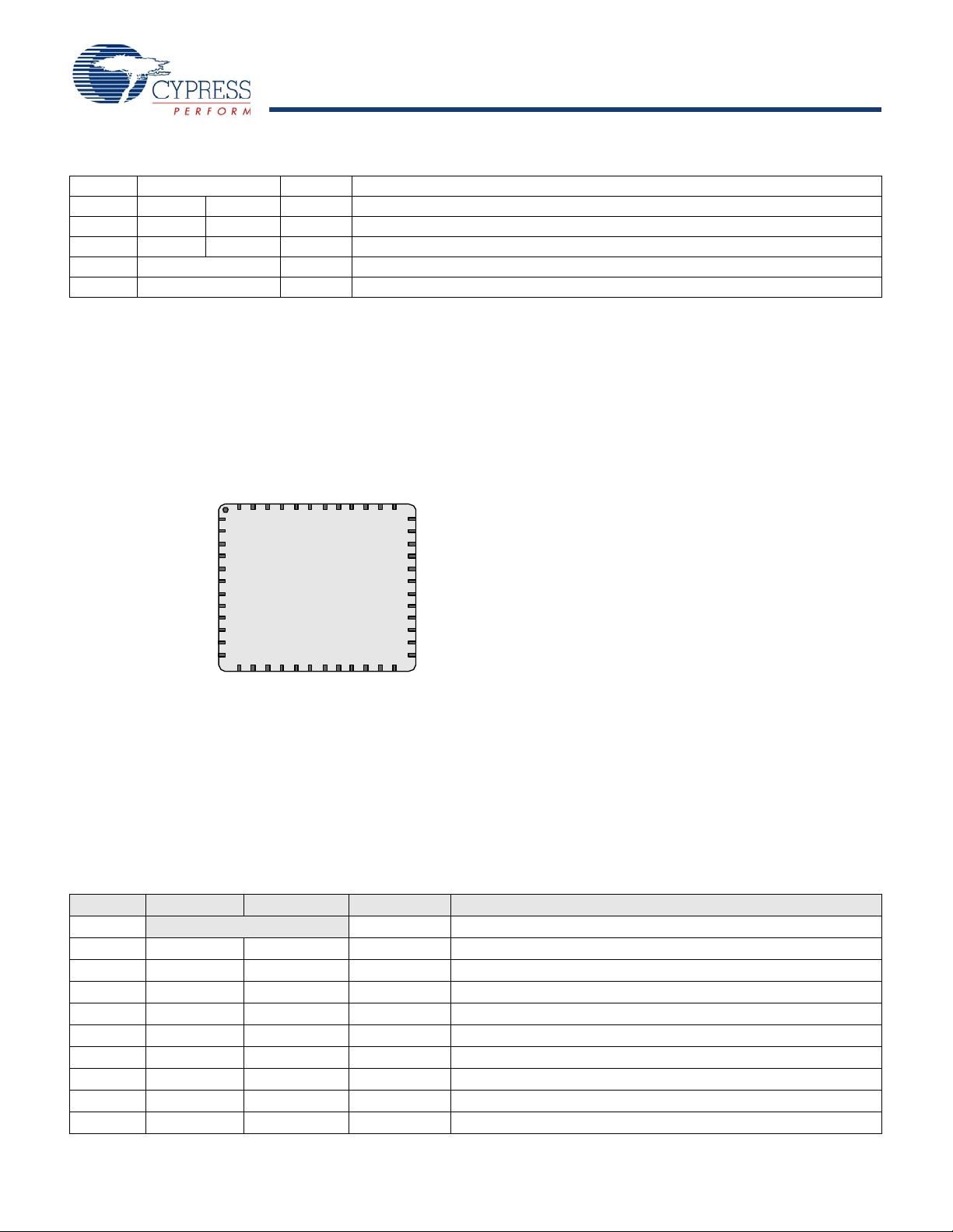
IDAC
Reference
Buffer
Vr
Cinternal
Analog Global Bus
Cap Sense Counters
Comparator
Mux
Mux
Refs
CapS ens e
Clock Select
Relaxation
Oscillator
(RO)
CSCLK
IMO
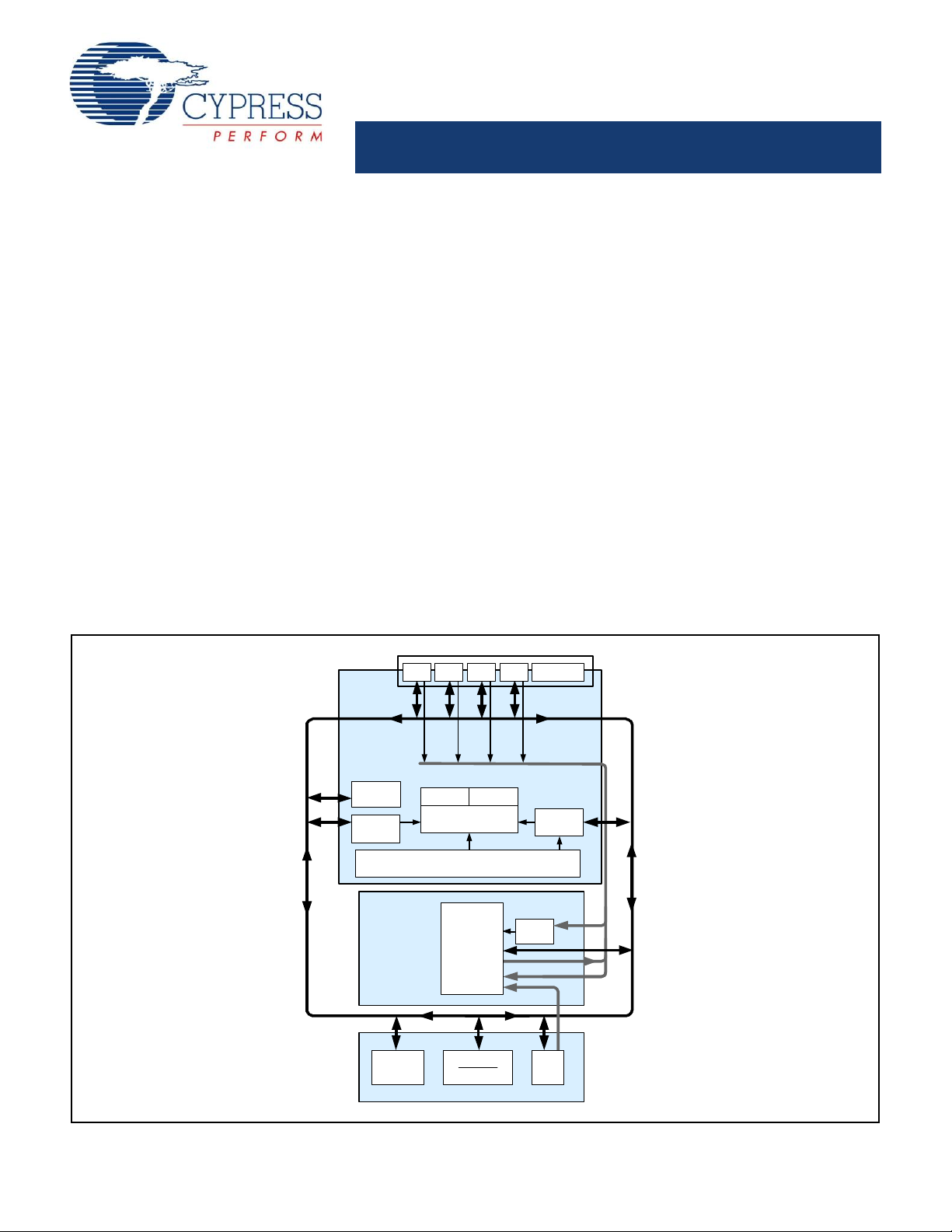
PSoC Functional Overview
The PSoC® family consists of many Mixed Signal Arrays with
On-Chip Controller devices. These devices are designed to
replace multiple traditional MCU based system components
with one low cost single chip programmable component. A
PSoC device includes configurable analog and digital blocks
and programmable interconnect. This architecture enables the
user to create customized peripheral configurations to match
the requirements of each individual application. Additionally, a
fast CPU, Flash program memory, SRAM data memory, and
configurable IO are included in a range of convenient pinouts.
The PSoC architecture for this device family, as shown in
Figure 1, is comprised of three main areas: the Core, the Sys-
tem Resources, and the CapSense Analog System. A common
versatile bus enables connection between IO and the analog
system. Each CY8C20x34 PSoC device includes a dedicated
CapSense block that provides sensing and scanning control cir
cuitry for capacitive sensing applications. Depending on the
PSoC package, up to 28 general purpose IO (GPIO) are also
included. The GPIO provide access to the MCU and analog
mux.
The PSoC Core
The PSoC Core is a powerful engine that supports a rich
instruction set. It encompasses SRAM for data storage, an
interrupt controller, sleep and watchdog timers, IMO (Internal
Main Oscillator), and ILO (Internal Low speed Oscillator). The
CPU core, called the M8C, is a powerful processor with sp eed s
up to 12 MHz. The M8C is a two MIPS, 8-bit Harvard architec
ture microprocessor.
System Resources provide additional capability such as a con figurable I2C slave or SPI master-slave communication inter-
face and various system resets supported by the M8C.
The Analog System is composed of the CapSense PSoC block
and an internal 1.8V analog reference. Together they supp ort
capacitive sensing of up to 28 inputs.
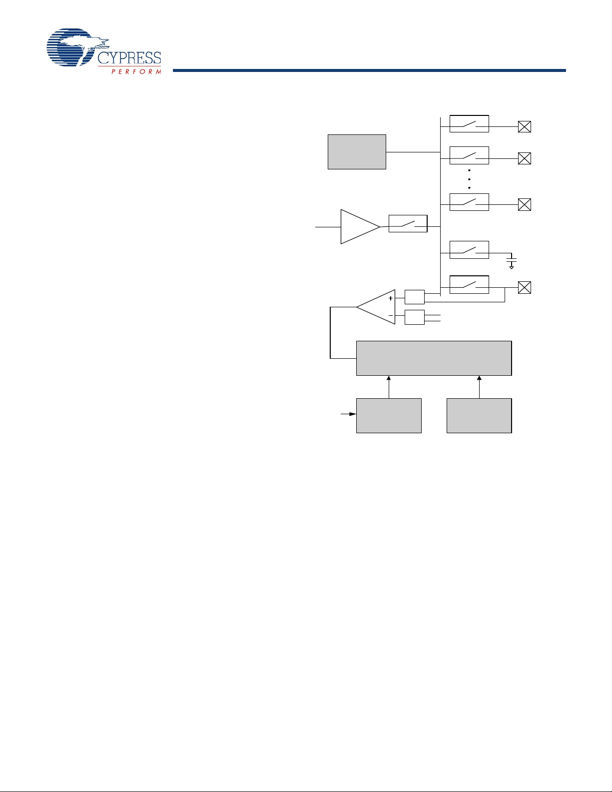
The CapSense Analog System
The Analog System contains the capacitive sensing hardware.
Several hardware algorithms are supported. This hardware per
forms capacitive sensing and scanning without requiring external components. Capacitive sensing is configurable on each
GPIO pin. Scanning of enabled CapSense pins is completed
quickly and easily across multiple ports.
Figure 1. Analog System Block Diagram
-
-
The Analog Multiplexer System
The Analog Mux Bus connects to every GPIO pin. Pins are connected to the bus individually or in any combination. Th e bus
also connects to the analog system for analysis with the
CapSense block comparator.
Switch control logic enables selected pins to precharge continuously under hardware control. This enables capacitive measurement for applications such as touch sensing. Other
multiplexer applications include:
■ Complex capacitive sensing interfaces such as sliders and
touch pads
-
■ Chip-wide mux that enables analog input from any IO pin
■ Crosspoint connection between any IO pin combinations
When designing capacitive sensing applications, refer to the latest signal-to-noise signal level requi rements Application Notes,
found under
http://www.cypress.com >> DESIGN
RESOURCES >> Application Notes. In general, unless otherwise noted in the relevant Application Notes, the minimum signal-to-noise ratio (SNR) requirement for CapSense applications
is 5:1.
Document Number: 001-05356 Rev. *D Page 2 of 34
[+] Feedback

CY8C20534, CY8C20434
CY8C20334, CY8C20234
Additional System Resources
Technical Training Modules
System Resources provide additional capability useful to complete systems. Additional resources include low voltage detection and power on reset. Brief statements describing the merits
of each system resource are presented below.
2
■ The I
■ Low Voltage Detection (LVD) interrupts signal the application
■ An internal 1.8V reference provides an absolute reference for
■ The 5V maximum input, 3V fixed output, low dropout regulator
C slave or SPI master-slave module provides 50/100/400
kHz communication over two wires. SPI communication over
three or four wires run at speeds of 46.9 kHz to 3 MHz (lower
for a slower system clock).
of falling voltage levels, while the advanced POR (Power On
Reset) circuit eliminates the need for a system supervisor.
capacitive sensing.
(LDO) provides regulation for IOs. A register controlled bypass
mode enables the user to disable the LDO.
Getting Started
To understand the PSoC silicon read this datasheet and use the
PSoC Designer Integrated Development Environment (IDE).
This datasheet is an overview of the PSoC integrated circuit
and presents specific pin, register, and electrical specifications.
For in depth information, along with detailed programming infor
mation, refer to the PSoC Mixed Signal Array Technical Refer-
ence Manual on the web at http://www.cypress.com/psoc.
For up to date Ordering, Packaging, and Electrical Specification
information, refer to the latest PSoC device datasheets on the
http://www.cypress.com.
web at
Free PSoC technical training modules are available for new
users to PSoC. Training modules cover designing, debugging,
advanced analog, and CapSense. Go to
http://www.cypress.com/techtrain.
Consultants
Certified PSoC Consultants offer everything from technical
assistance to completed PSoC designs. To contact or become a
PSoC Consultant go to
Support located on the left side of the web page and select
CYPros Consultants.
http://www.cypress.com, click on Design
Technical Support
PSoC application engineers take pride in fast and accurate
response. They are available with a four hour guaranteed
response at
http://www.cypress.com/support/login.cfm.
Application Notes
A long list of application notes assist you in every aspect of your
design effort. To view the PSoC application notes, go to the
http://www.cypress.com and select Application Notes under the
Design Resources list located in the center of the web page.
Application notes are sorted by date by default.
Development Tools
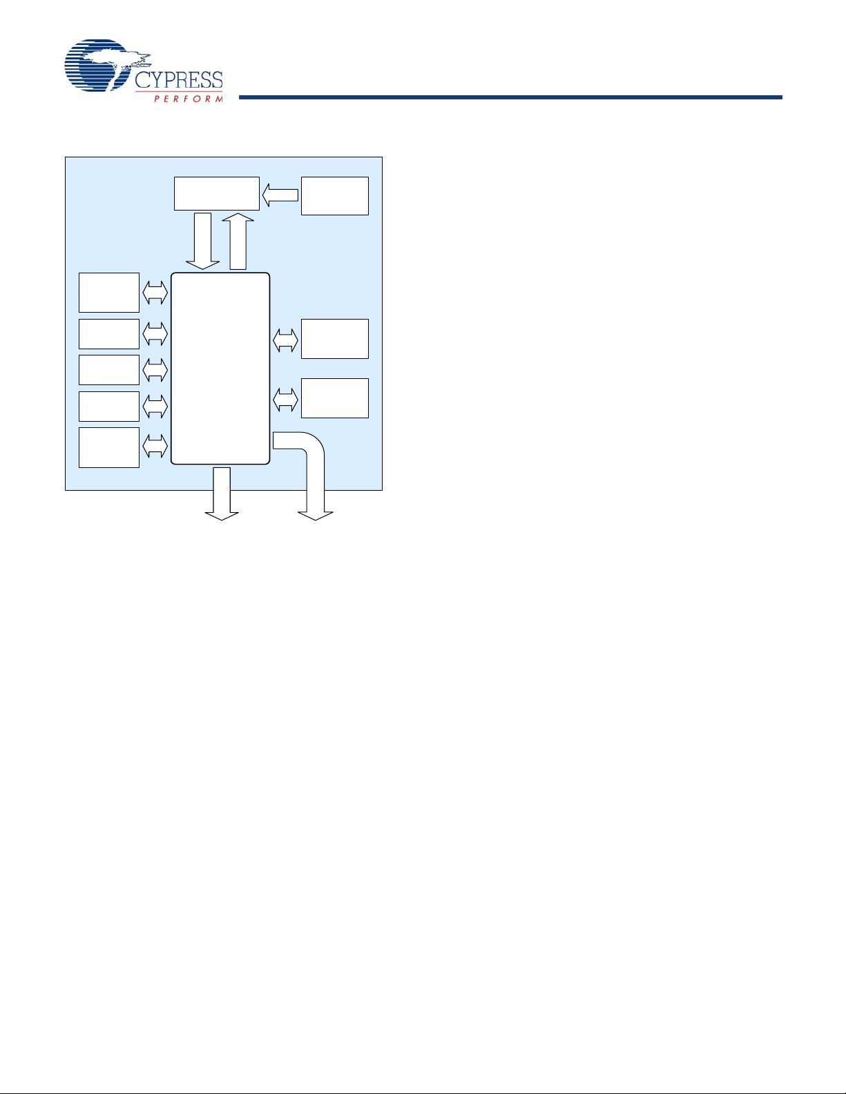
PSoC Designer is a Microsoft® Windows based, integrated
Development Kits
Development Kits are available from the following distributors:
Digi-Key, Avne t, Arrow, and Future. The Cypress Online Store
contains development kits, C compilers, and all accessories for
PSoC development. Go to the Cypress Online Store web site at
http://www.cypress.com, click the Online Store shopping cart
icon at the bottom of the web page and click PSoC (Program-
mable System-on-Chip) to view a current list of available items.
Document Number: 001-05356 Rev. *D Page 3 of 34
development environment for the Programmable System-on-Chip (PSoC) devices. The PSoC Designer IDE and
application runs on Windows NT 4.0, Windows 2000, Windows
Millennium (Me), or Windows XP. For more information, see
Figure 2 on page 4.
PSoC Designer helps the customer to select an operating configuration for the PSoC, write application code that uses the
PSoC, and debug the application. This system provides design
database management by project, an integrated debugger with
In-Circuit Emulator, in-system programming support, and the
CYASM macro assembler for the CPUs.
PSoC Designer also supports a high level C language compiler
developed specifically for the devices in the family.
[+] Feedback
CY8C20534, CY8C20434
CY8C20334, CY8C20234
Figure 2. PSoC Designer Subsystems
Commands
Results
PSoC
Designer
Core
Engine
PSoC
Configuration
Sheet
Manufacturing
Information
File
Device
Database
Importable
Design
Database
Graphical Designer
Interfac e
Context
Sensitive
Help
Project
Database
Application
Database
User
Modules
Library
PSoC
Designer
PSoC Designer Software Subsystems
Assembler
The macro assembler enables the assembly code for seamless
merging with C code. The link lib raries automatically use abso
lute addressing or are compiled in relative mode and linked with
other software modules to get absolute a ddr e ssing .
C Language Compiler
C language compiler supports the PSoC family of devices. It
quickly enables you to create complete C programs for the
PSoC family devices.
The embedded optimizing C compiler provides all the features
of C language tailored to the PSoC architecture. It comes com
plete with embedded libraries providing port and bus operations, standard keypad and display support, and extended math
functionality.
Debugger
The PSoC Designer Debugger subsystem provides hardware
in-circuit emulation, enabling the designer to test the program in
a physical system while providing an internal view of the PSoC
device. Debugger commands enable the designer to read the
program, read and write data memory, read and write IO regis
ters, read and write CPU registers, set and clear breakpoints,
and provide program run, halt, and step control. The debugger
also enables the designer to create a trace buffer of registers
and memory locations of interest.
-
-
-
Device Editor
The device editor subsystem enables the user to select different
on board analog and digital components called user modules
using the PSoC blocks. Examples of user modules are ADCs,
DACs, Amplifiers, and Filters.
The device editor also supports easy development of multiple
configurations and dynamic reconfiguration. Dynamic reconfiguration enables changing configurations at run time.
PSoC Designer sets up power on initialization tables for
selected PSoC block configurations and creates source code
for an application framework. The framework contains software
to operate the selected components. If the project uses more
than one operating configuration, then it contains routines to
switch between different sets of PSoC block configurations at
run time. PSoC Designer prints out a configuration sheet for a
given project configuration for use during application program
ming in conjunction with the device datasheet. Once the framework is generated, the user adds application specific code to
flesh out the framework. It is also possible to change the
selected components and regenerate the framework.
Application Editor
Application Editor edits C language and Assembly language
source code. It also assembles, compiles, links, and builds.
Online Help System
The online help system displays online and context sensitive
help for the user. Designed for procedural and quick reference,
each functional subsystem has its own context sensitive help.
This system also provides tutorials and links to FAQs and an
Online Support Forum to aid the designer to get started.
Hardware Tools
In-Circuit Emulator
A low cost, high functionality ICE (In-Circuit Emulator) is available for development support. This hardware has the capability
to program single devices.
The emulator consists of a base unit that connects to the PC by
-
way of a USB port. The base unit is universal and operates with
all PSoC devices. Emulation pods for each device family are
available separately. The emulation pod takes the place of the
PSoC device in the target board and performs full speed (24
MHz) operation.
Document Number: 001-05356 Rev. *D Page 4 of 34
[+] Feedback
CY8C20534, CY8C20434
CY8C20334, CY8C20234
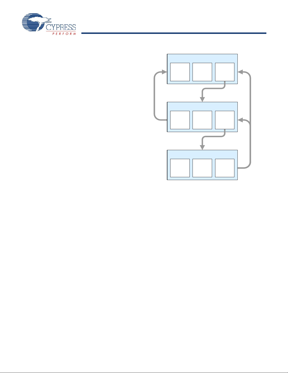
Designing with User Modules
Debugger
Interface
to ICE
Application Editor
Device Editor
Project
Manager
Source
Code
Editor
Storage
Inspector
User
Module
Selection
Placement
and
Parameter
-ization
Generate
Applic ation
Build
All
Event &
Breakpoint
Manager
Build
Manager
Source
Code
Generator
Figure 3. User Module and Source Code Development Flows
The development process for the PSoC device differs from that
of a traditional fixed function microprocessor. The configurable
analog and digital hardware blocks give the PSoC architecture
a unique flexibility. It pays dividends in managing specification
change during development and by lowering inventory costs.
These configurable resources are called PSoC Blocks. They
implement a wide variety of user selectable functions. Each
block has several registers to determine their function and con
-
nectivity to other blocks, multiplexers, buses, and to the IO pins.
Iterative development cycles permit you to adapt the hardware
and the software. This substantially lowers the risk of selecting
a different part to meet the final design requirements.
To speed the development process, the PSoC Design er Integrated Development Environment (IDE) provides a library of
pre-built and pre-tested hardware peripheral functions called as
User Modules. User modules make selecting and implementing
peripheral devices simple. They come in analog, digital, and
mixed signal varieties.
Each user module establishes the basic register settings to
implement the selected function. It also provides parameters to
tailor its precise configuration to a particular application. For
example, a Pulse Width Modulator user module configures one
or more digital PSoC blocks, one for each 8-bits of resolution.
The user module parameters permit you to establish the pulse
width and duty cycle. User modules also provide tested soft
ware to cut the development time. The user module application
programming interface (API) provides high level functions to
control and respond to hardware events at run time. The API
also provides optional interrupt service routines to adapt as
needed.
The API functions are documented in user module datasheets
that are viewed directly in the PSoC Designer IDE. These
datasheets explain the internal operation of the user module
and provide performance specifications. Each datasheet
describes the use of each user module parameter and docu
ments the setting of each register controlled by the user module.
The development process starts when you open a new project
and bring up the Device Editor, a graphical user interface (GUI)
for configuring the hardware. Select the user modules you need
for your project and map them on to the PSoC blocks with
point-and-click simplicity. Then, build signal chains by intercon
necting the user modules to each other and the IO pins. At this
stage, configure the clock source connections and enter parameter values directly or by selecting values from the drop down
menus. When the hardware configuration is ready for testing or
moves on to developing code for the project, perform the “Gen
erate Application” step. The PSoC Designer generates the
source code that automatically configures the device to your
specification and provides the high level user module API func
Now write the main program and any sub-routines using PSoC
Designer’s Application Editor subsystem. The Application Edi
tor includes a Project Manager that enables to open the project
source code files (including all generated code files) from a
hierarchal view. The source code editor provides syntax color
ing and advanced edit features for both C and assembly lan guage. File search capabilities include simple string searches
and recursive “grep-style” patterns. A single mouse click
invokes the Build Manager. It employs a professional strength
“makefile” system to automatically analyze all file dependencies
-
and run the compiler and assembler as necessary. Project level
options control optimization strategies used by the compiler and
linker. Syntax errors are displayed in a console window. Double
click the error message to show the offending line of source
code. When all is correct, the linker builds a HEX file image suit
able for programming.
The last step in the development process takes place inside the
-
PSoC Designer’s Debugger subsystem. The Debugger downloads the HEX image to the In-Circuit Emulator (ICE) where it
runs at full speed. Debugger capabilities rival those of systems
costing many times more. In addition to traditional single step,
run-to-breakpoint, and watch variable features, the Debugger
-
provides a large trace buffer. This enables to define complex
breakpoint events such as monitoring address and data bus
values, memory locations, and external signals.
-
tions.
Document Number: 001-05356 Rev. *D Page 5 of 34
-
-
-
[+] Feedback
CY8C20534, CY8C20434
CY8C20334, CY8C20234
Document Conventions
Acronyms Used
The following table lists the acronyms that are used in this document.
Acronym Description
AC alternating current
API application programming interface
CPU central processing unit
DC direct current
GPIO general purpose IO
GUI graphical user interface
ICE in-circuit emulator
ILO internal low speed oscillator
IMO internal main oscillator
IO input or output
LSb least significant bit
LVD low voltage detect
MSb most significant bit
POR power on reset
PPOR precision power on reset
PSoC® Programmable System-on-Chip™
SLIMO slow IMO
SRAM static random access memory
Units of Measure
A units of measure table is located in the Electrical Specifications section. Table 6 on page 13 lists all the abbreviations used
to measure the PSoC devices.
Numeric Naming
Hexadecimal numbers are represented with all letters in upper case with an appended lowercase ‘h’ (for example, ‘14h’ or
‘3Ah’). Hexadecimal numbers are also represented by a ‘0x’
prefix, the C coding convention. Binary numbers have an
appended lowercase ‘b’ (For example, 01010100b or
01000011b). Numbers not indicated by an ‘h’, ‘b’, or 0x are dec
imals.
-
Document Number: 001-05356 Rev. *D Page 6 of 34
[+] Feedback
CY8C20534, CY8C20434
CY8C20334, CY8C20234
Pinouts
QFN
(Top View)
AI, P2 [5 ]
AI, I2C SCL, SPI SS, P1[7]
AI, I2C SDA, SPI MISO, P1[5]
AI, SPI CLK, P1[3]
1
2
3
4
11
10
9
161514
13
P0[3], AI
P0[7], AI
Vdd
P0[4], AI
CLK, I2C SCL, SPI MOSI P1[1]
AI, DATA, I2C SDA, P1[0]
P1[2], AI
AI, P2 [1 ]
P1[4], AI, EXT CLK
XRES
P0[1], AI
Vss
12
567
8
Notes
1. These are the ISSP pins, that are not High Z at POR (Power On Reset). See the PSoC Mixed Signal Array Technical Reference Manual for details.
2. The center pad on the QFN package is connected to ground (Vss) for best mechanical, thermal, and electrical performance. If not conn ected to ground, it is electrically
floated and not connected to any other signal.
This section describes, lists, and illustrates the CY8C20234, CY8C20334, CY8C20434, and CY8C2053 4 PSoC device pins and
pinout configurations.
The CY8C20x34 PSoC device is available in a variety of packages that are listed a nd shown in the fol lowing tables. Every port pin
(labeled with a “P”) is capable of Digital IO and connection to the common analog bus. However, Vss, Vdd, and XRES are not capable of Digital IO.
16-Pin Part Pinout
Figure 4. CY8C20234 16-Pin PSoC Device
Table 1. 16-Pin Part Pinout (QFN
Pin No.
1 IO I P2[5]
2 IO I P2[1]
3 IOH I P1[7] I2C SCL, SPI SS.
4 IOH I P1[5] I2C SDA, SPI MISO.
5 IOH I P1[3] SPI CLK .
6 IOH I P1[1] CLK
7 Power Vss Ground connection.
8 IOH I P1[0] DATA
9 IOH I P1[2]
10 IOH I P1[4] Optional external clock input (EXTCLK).
11 Input XRES Active high external reset with internal pull down.
12 IO I P0[4]
13 Power Vdd Supply voltage.
14 IO I P0[7]
15 IO I P0[3] Integrating input.
16 IO I P0[1]
A = Analog, I = Input, O = Output, OH = 5 mA High Output Drive
Type
Digital Analog
[2]
)
Name Description
[1]
, I2C SCL, SPI MOSI.
[1]
, I2C SDA.
Document Number: 001-05356 Rev. *D Page 7 of 34
[+] Feedback
CY8C20534, CY8C20434
CY8C20334, CY8C20234
24-Pin Part Pinout
QFN
(Top View)
AI, P2[5]
AI, I2C SCL, SPI SS, P1[7]
AI, I2C SDA, SPI MISO, P1[5]
AI, SPI CLK, P1[3]
1
2
3
4
5
6
18
17
16
15
14
13
P0[2], A I
P0[0], A I
24
23
22
21
20
19
P0[3], AI
P0[5], AI
P0[7], AI
Vdd
P0[4], AI
7
8
9
10
11
12
SPI MOSI, P1[1]
AI, DATA*, I2C SDA, P1[0]
AI, P1[2]
AI, P2[3]
AI, P2[1]
NC
P1[6], AI
AI, EXTCLK, P1[4]
XRES
P2[0], AI
P0[6], AI
AI, CLK*, I2C SCL
P0[1], AI
Vss
Figure 5. CY8C20334 24-Pin PSoC Device
Table 2. 24-Pin Part Pinout (QFN
Pin No.
1 IO I P2[5]
2 IO I P2[3]
3 IO I P2[1]
4 IOH I P1[7] I2C SCL, SPI SS.
5 IOH I P1[5] I2C SDA, SPI MISO.
6 IOH I P1[3] SPI CLK.
7 IOH I P1[1] CLK
8 NC No connection.
9 Power Vss Ground connection.
10 IOH I P1[0] DATA
11 IOH I P1[2]
12 IOH I P1[4] Optional external clock input (EXTCLK).
13 IOH I P1[6]
14 Input XRES Active high external reset with internal pull down.
15 IO I P2[0]
16 IO I P0[0]
17 IO I P0[2]
18 IO I P0[4]
19 IO I P0[6] Analog bypass.
20 Power Vdd Supply voltage.
21 IO I P0[7]
22 IO I P0[5]
23 IO I P0[3] Integrating input.
24 IO I P0[1]
CP Power Vss Center pad is connected to ground.
A = Analog, I = Input, O = Output, OH = 5 mA High Output Drive
Document Number: 001-05356 Rev. *D Page 8 of 34
Type
Digital Analog
[2]
)
Name Description
[1]
, I2C SCL, SPI MOSI.
[1]
, I2C SDA.
[+] Feedback
CY8C20534, CY8C20434
CY8C20334, CY8C20234
28-Pin Part Pinout
A, I, M, P0[7]
A, I, M, P0[5]
A, I, M, P0[3]
A, I, M, P0[1]
M, P2[7]
M, P2[5]
M, P2[3]
M, P2[ 1]
Vss
M, I2C SCL, P1[7]
M, I2C SDA, P1[5]
M, P1[3]
M, I2C SCL, P1[1]
Vss
Vdd
P0[6], A, I, M
P0[4], A, I, M
P0[2], A, I, M
P0[0], A, I, M
P2[6], M
P2[4], M
P2[2], M
P2[0], M
XRES
P1[6], M
P1[4], EXTCLK, M
P1[2], M
P1[0], I2C SDA, M
SSOP
1
2
3
4
5
6
7
8
9
10
11
12
13
14
28
27
26
25
24
23
22
21
20
19
18
17
16
15
Figure 6. CY8C20534 28-Pin PSoC Device
Table 3. 28-Pin Part Pinout (SSOP )
Pin No.
1 IO I, M P0[7] Analog column mux input.
2 IO I, M P0[5] Analog column mux input and column output.
3 IO I, M P0[3] Analog column mux input and column output, integrating input.
4 IO I, M P0[1] Analog column mux input, integrating input.
5 IO M P2[7]
6 IO M P2[5]
7 IO I, M P2[3] Direct switched capacitor block input.
8 IO I, M P2[1] Direct switched capacitor block input.
9 Power Vss Ground connection.
10 IO M P1[7] I2C Serial Clock (SCL).
11 IO M P1[5] I2C Serial Data (SDA).
12 IO M P1[3]
13 IO M P1[1] I2C Serial Clock (SCL), ISSP-SCLK
14 Power Vss Ground connection.
15 IO M P1[0] I2C Serial Data (SDA), ISSP-SDATA
16 IO M P1[2]
17 IO M P1[4] Optional External Clock Input (EXTCLK).
18 IO M P1[6]
19 Input XRES Active high external reset with internal pull down.
20 IO I, M P2[0] Direct switched capacitor block input.
21 IO I, M P2[2] Direct switched capacitor block input.
22 IO M P2[4]
23 IO M P2[6]
24 IO I, M P0[0] Analog column mux input.
25 IO I, M P0[2] Analog column mux input.
26 IO I, M P0[4] Analog column mux input
27 IO I, M P0[6] Analog column mux input.
28 Power Vdd Supply voltage.
A = Analog, I = Input, O = Output, OH = 5 mA High Output Drive.
Document Number: 001-05356 Rev. *D Page 9 of 34
Type
Digital Analog
Name Description
[1]
.
[1]
.
[+] Feedback
CY8C20534, CY8C20434
CY8C20334, CY8C20234
32-Pin Part Pinout
AI, P0[1]
AI, P2[7]
AI, P2[5]
AI, P2[3]
AI, P2[1]
AI, P3[3]
QFN
(Top View)
9
101112
131415
16
1
2
3
4
5
6
7
8
24
23
22
21
20
19
18
17
32313029282726
25
Vss
P0[3], AI
P0[7], AI
Vdd
P0[6], AI
P0[4], AI
P0[2], AI
AI, P3[1]
SPI SS, P1[7]
P0[ 0 ], AI
P2[ 6 ], AI
P3[ 0 ], AI
XRES
AI, I2C SDA, SPI MISO, P1[5]
AI, SPI CLK, P1[3]
AI, CLK*, I2C SCL, SPI MOSI, P1[1]
Vss
AI, DATA*, I2C SDA, P1[0]
AI, P1[2]
AI, EXTCLK, P1[4]
AI, P1[6]
P2[ 4 ], AI
P2[ 2 ], AI
P2[ 0 ], AI
P3[ 2 ], AI
P0[5], AI
AI, I2C SCL
Figure 7. CY8C20434 32-Pin PSoC Device
Table 4. 32-Pin Part Pinout (QFN
Pin No.
Type
Digital Analog
[2]
)
Name Description
1 IO I P0[1]
2 IO I P2[7]
3 IO I P2[5]
4 IO I P2[3]
5 IO I P2[1]
6 IO I P3[3]
7 IO I P3[1]
8 IOH I P1[7] I2C SCL, SPI SS.
9 IOH I P1[5] I2C SDA, SPI MISO.
10 IOH I P1[3] SPI CLK.
11 IOH I P1[1] CLK
[1]
, I2C SCL, SPI MOSI.
12 Power Vss Ground connection.
13 IOH I P1[0] DATA
[1]
, I2C SDA.
14 IOH I P1[2]
15 IOH I P1[4] Optional external clock input (EXTCLK).
16 IOH I P1[6]
17 Input XRES Active high external reset with internal pull down.
18 IO I P3[0]
19 IO I P3[2]
20 IO I P2[0]
21 IO I P2[2]
22 IO I P2[4]
23 IO I P2[6]
24 IO I P0[0]
25 IO I P0[2]
26 IO I P0[4]
27 IO I P0[6] Analog bypass.
Document Number: 001-05356 Rev. *D Page 10 of 34
[+] Feedback
CY8C20534, CY8C20434
CY8C20334, CY8C20234
Table 4. 32-Pin Part Pinout (QFN
OCD
QFN
(Top View)
NC
Vss
P0[3], AI
P0[5], AI
P0[7], AI
OCDE
OCDO
Vdd
P0[6], AINCNC
NC
10
11
12
NC
AI, P0[1]
AI, P2[7]
AI, P2[5]
AI, P2[3]
AI, P2[1]
AI, P3[3]
AI, P3[1]
AI, I2C SCL, SPI SS, P1[7]
AI, I2C SDA, SPI MISO, P1[5]
NC
NC
35
34
33
32
31
30
29
28
27
26
25
36
4847464544434241403938
37
P0[2], AI
P0[0], AI
P2[6], AI
P2[4], AI
P2[2], AI
P2[0], AI
P3[2], AI
P3[0], AI
XRES
P1[6], AI
P1[4], EXTCLK, AI
P0[4], AI
1
2
3
4
5
6
7
8
9
13
14
151617181920212223
24
NC
NC
AI, SPI CLK, P1[3]
AI, CLK*, I2C SCL, SPI MOSI, P1[1]
Vss
CCLK
HCLK
AI, DATA*, I2C SDA, P1[0]
AI, P1[2]
NCNCNC
[2]
) (continued)
28 Power Vdd Supply voltage.
29 IO I P0[7]
30 IO I P0[5]
31 IO I P0[3] Integrating input.
32 Power Vss Ground connection.
CP Power Vss Center pad is connected to ground.
A = Analog, I = Input, O = Output, OH = 5 mA High Output Drive.
48-Pin OCD Part Pinout
The 48-Pin QFN part table and pin diagram is for the CY8C20000 On-Chip Debug (OCD) PSoC device. This part is only used for
in-circuit debugging. It is NOT available for production.
Figure 8. CY8C20000 OCD PSoC Device
Table 5. 48-Pin OCD Part Pinout (QFN
Pin No. Digital Analog Name Description
1 NC No connection.
2 IO I P0[1]
3 IO I P2[7]
4 IO I P2[5]
5 IO I P2[3]
6 IO I P2[1]
7 IO I P3[3]
8 IO I P3[1]
9 IOH I P1[7] I2C SCL, SPI SS.
10 IOH I P1[5] I2C SDA, SPI MISO.
Document Number: 001-05356 Rev. *D Page 11 of 34
[2]
)
[+] Feedback

CY8C20534, CY8C20434
CY8C20334, CY8C20234
Table 5. 48-Pin OCD Part Pinout (QFN
Pin No. Digital Analog Name Description
11 IO I P0[1]
12 NC No connection.
13 NC No connection.
14 NC No connection.
15 NC No connection.
16 IOH I P1[3] SPI CLK.
17 IOH I P1[1] CLK
18 Power Vss Ground connection.
19 CCLK OCD CPU clock output.
20 HCLK OCD high speed clock output.
21 IOH I P1[0] DATA
22 IOH I P1[2]
23 NC No connection.
24 NC No connection.
25 NC No connection.
26 IOH I P1[4] Optional external clock input (EXTCLK).
27 IOH I P1[6]
28 Input XRES Active high external reset with internal pull down.
29 IO I P3[0]
30 IO I P3[2]
31 IO I P2[0]
32 IO I P2[2]
33 IO I P2[4]
34 IO I P2[6]
35 IO I P0[0]
36 IO I P0[2]
37 NC No connection.
38 NC No connection.
39 NC No connection.
40 IO I P0[6] Analog bypass.
41 Power Vdd Supply voltage.
42 OCDO OCD odd data output.
43 OCDE OCD even data IO.
44 IO I P0[7]
45 IO I P0[5]
46 IO I P0[3] Integrating input.
47 Power Vss Ground connection.
48 NC No connection.
CP Power Vss Center pad is connected to ground.
A = Analog, I = Input, O = Output, NC = No Connection H = 5 mA High Output Drive.
[2]
) (continued)
[1]
, I2C SCL, SPI MOSI.
[1]
, I2C SDA.
Document Number: 001-05356 Rev. *D Page 12 of 34
[+] Feedback

CY8C20534, CY8C20434
CY8C20334, CY8C20234
Electrical Specifications
5.25
4.75
3.00
750 kHz
12 MHz
CPU Frequency
Vdd Voltage
5.25
4.75
3.00
750 kHz
6 MHz 12 MHz
IMO Frequency
Vdd Voltage
3.60
3 MHz
2.40
SLIMO
Mode=1
2.40
3 MHz
V
a
l
i
d
O
p
e
r
a
t
i
n
g
R
e
g
i
o
n
SLIMO
Mode=1
SLIMO
Mode=0
SLIMO
Mode=1
SLIMO
Mode=0
2.70
SLIMO
Mode=1
SLIMO
Mode=0
2.70
6 MHz
This section presents the DC and AC electrical specifications of the CY8C20234, CY8C20334, CY8C20434, and CY8C20534 PSoC
devices. For the latest electrical specifications, check the most recent datasheet by visiting the web at http://www.cypress.com/psoc.
Specifications are valid for -40oC ≤ TA ≤ 85oC and TJ ≤ 100oC as specified, except where mentioned.
Refer to Table 16 on page 19 for the electrical specifications on the internal main oscillator (IMO) using SLIMO mode.
Figure 9. Voltage versus CPU Frequency and IMO Frequency Trim Optio ns
Table 6 lists the units of measure that are used in this section.
Table 6. Units of Measure
Symbol Unit of Measure Symbol Unit of Measure
o
C degree Celsius μW microwatts
dB decibels mA milliampere
fF femto farad ms millisecond
Hz hertz mV millivolts
KB 1024 bytes nA nanoampere
Kbit 1024 bits ns nanosecond
kHz kilohertz nV nanovolts
kΩ kilohm W ohm
MHz megahertz pA picoampere
MΩ megaohm pF picofarad
μA microampere pp peak-to-peak
μF microfarad ppm parts per million
μH microhenry ps picosecond
μs microsecond sps samples per second
μV microvolts s sigma: one standard deviation
μVrms microvolts root-mean-square V volts
Document Number: 001-05356 Rev. *D Page 13 of 34
[+] Feedback

CY8C20534, CY8C20434
CY8C20334, CY8C20234
Absolute Maximum Ratings
Table 7. Absolute Maximum Ratings
Symbol Description Min Typ Max Units Notes
T
STG
Storage Temperature -55 25 +100
o
C Higher storage temperatures reduces
data retention time. Recommended
storage temperature is +25oC ± 25oC.
Extended duration storage tempera
tures above 65oC degrades reliability.
T
A
Ambient Temperature with Power Applied -40 – +85
o
C
Vdd Supply Voltage on Vdd Relative to Vss -0.5 – +6.0 V
V
V
I
MIO
IO
IOZ
DC Input Voltage Vss -
0.5
DC Voltage Applied to Tri-state Vss -
0.5
– Vdd +
0.5
– Vdd +
0.5
V
V
Maximum Current into any Port Pin -25 – +50 mA
ESD Electro Static Discharge Voltage 2000 – – V Human Body Model ESD.
LU Latch up Current – – 200 mA
Operating Temperature
Table 8. Operating Temperature
Symbol Description Min Typ Max Units Notes
T
A
T
J
Ambient Temperature -40 – +85
Junction Temperature -40 – +100
o
C
o
C The temperature rise from ambient to
junction is package specific. See
Table 14 on page 17. The user must
limit the power consumption to comply
with this requirement.
-
Document Number: 001-05356 Rev. *D Page 14 of 34
[+] Feedback

CY8C20534, CY8C20434
CY8C20334, CY8C20234
DC Electrical Characteristics
DC Chip Level Specifications
Table 9 lists guaranteed maximu m and minimum specifications for the voltage and temperature ranges: 4.75V to 5.25V and -40°C ≤
TA ≤ 85°C, 3.0V to 3.6V and -40°C ≤ TA ≤ 85°C, or 2.4V to 3.0V and -40°C ≤ TA ≤ 85°C, respectively. Typical parameters apply to 5V,
3.3V, or 2.7V at 25°C. These are for design guidance only.
Table 9. DC Chip Level Specifications
Sym-
bol
Description Min Typ Max Units Notes
Vdd Supply Voltage 2.40 – 5.25 V See Table 14 on page 17.
I
DD12
I
DD6
I
SB27
Supply Current, IMO = 12 MHz – 1.5 2.5 mA Conditions are Vdd = 3.0V , TA = 25oC,
CPU = 12 MHz.
Supply Current, IMO = 6 MHz – 1 1.5 mA Conditions are Vdd = 3.0V, TA = 25oC,
CPU = 6 MHz.
Sleep (Mode) Current with POR, LVD, Sleep
– 2.6 4. μA Vdd = 2.55V, 0oC ≤ TA ≤ 40oC.
Timer, WDT, and Internal Slow Oscillator
Active. Mid Temperature R ange.
I
SB
Sleep (Mode) Current with POR, LVD, Sleep
Timer, WDT, and Internal Slow Oscillator
– 2.8 5 μA Vdd = 3.3V, -40oC ≤ TA ≤ 85oC.
Active.
DC General Purpose IO Specifications
Unless otherwise noted, the Table 10 lists guaranteed maximum and minimum specifications for the voltage and temperature
ranges: 4.75V to 5.25V and -40°C ≤ TA ≤ 85°C, 3.0V to 3.6V and -40°C ≤ TA ≤ 85°C, or 2.4V to 3.0V and -40°C ≤ TA ≤ 85°C, respectively. Typical parameters apply to 5V, 3.3V, and 2.7V at 25°C. These are for design guidance only.
Table 10. 5V and 3.3V DC GPIO Specifications
Symbol Description Min Typ Max Units Notes
R
V
V
V
V
V
V
V
V
V
PU
OH1
OH2
OH3
OH4
OH5
OH6
OH7
OH8
OH9
Pull Up Resistor 4 5.6 8 kΩ
High Output Voltage
Port 0, 2, or 3 Pins
High Output Voltage
Port 0, 2, or 3 Pins
High Output Voltage
Port 1 Pins with LDO Regulator Disabled
High Output Voltage
Port 1 Pins with LDO Regulator Disabled
High Output Voltage
Vdd -
– – V IOH < 10 μA, Vdd > 3.0V, maximum of
0.2
Vdd -
– – V IOH = 1 mA, Vdd > 3.0V, maximum of
0.9
Vdd -
– – V IOH < 10 μA, Vdd > 3.0V, maximum of
0.2
Vdd -
– – V IOH = 5 mA, Vdd > 3.0V, maximum of
0.9
2.75 3.0 3.2 V IOH < 10 μA, Vdd > 3.1V, maximum of
Port 1 Pins with 3.0V LDO Regulator Enabled
High Output Voltage
2.2 – – V IOH = 5 mA, Vdd > 3.1V, maximum of
Port 1 Pins with 3.0V LDO Regulator Enabled
High Output Voltage
2.1 2.4 2.5 V IOH < 10 μA, Vdd > 3.0V, maximum of
Port 1 Pins with 2.4V LDO Regulator Enabled
High Output Voltage
2.0 – – V IOH < 200 μA, Vdd > 3.0V, maximum
Port 1 Pins with 2.4V LDO Regulator Enabled
High Output Voltage
1.6 1.8 1.95 V IOH < 10 μA.
Port 1 Pins with 1.8V LDO Regulator Enabled
20 mA source current in all IOs.
20 mA source current in all IOs.
10 mA source current in all IOs.
20 mA source current in all IOs.
4 IOs all sourcing 5 mA.
20 mA source current in all IOs.
20 mA source current in all IOs.
of 20 mA source current in all IOs.
3.0V ≤ Vdd ≤ 3.6V.
0oC ≤ TA ≤ 85oC.
Maximum of 20 mA source current in
all IOs.
Document Number: 001-05356 Rev. *D Page 15 of 34
[+] Feedback

CY8C20534, CY8C20434
CY8C20334, CY8C20234
Table 10. 5V and 3.3V DC GPIO Specifications (continued)
V
OH10
High Output Voltage
Port 1 Pins with 1.8V LDO Regulator Enabled
1.5 – – V IOH < 100 μA.
3.0V ≤ Vdd ≤ 3.6V.
0oC ≤ TA ≤ 85oC.
Maximum of 20 mA source current in
all IOs.
V
OL
Low Output Voltage – – 0.75 V IOL = 20 mA, Vdd > 3.0V , maximum of
60 mA sink current on even port pins
(for example, P0[2] and P1[4]) and 60
mA sink current on odd port pins (for
example, P0[3] and P1[5]).
V
V
V
I
C
C
IL
IH
H
IL
IN
OUT
Input Low Voltage – – 0.8 V 3.6V ≤ Vdd ≤ 5.25V.
Input High Voltage 2.0 – V 3.6V ≤ Vdd ≤ 5.25V.
Input Hysteresis Voltage – 140 – mV
Input Leakage (Absolute Value) – 1 – nA Gross tested to 1 μA.
Capacitive Load on Pins as Input 0.5 1.7 5 pF Package and pin dependent Temper-
ature = 25oC.
Capacitive Load on Pins as Output 0.5 1.7 5 pF Packa ge and pin dependent Temper-
ature = 25oC.
Table 11. 2.7V DC GPIO Specifications
Symbol Description Min Typ Max Units Notes
R
V
V
V
PU
OH1
OH2
OL
Pull Up Resistor 4 5.6 8 kΩ
High Output Voltage
Port 1 Pins with LDO Regulator Disabled
High Output Voltage
Port 1 Pins with LDO Regulator Disabled
Vdd -
0.2
Vdd -
0.5
– – V IOH < 10 μA, maximum of 10 mA
source current in all IOs.
– – V IOH = 2 mA, maximum of 10 mA source
current in all IOs.
Low Output Voltage – – 0.75 V IOL = 10 mA, maximum of 30 mA sink
current on even port pins (for example,
P0[2] and P1[4]) and 30 mA sink
current on odd port pins (for example,
P0[3] and P1[5]).
V
OLP1
Low Output Voltage Port 1 Pins – – 0.4 V IOL=5 mA
Maximum of 50 mA sink current on
even port pins (for example, P0[2] and
P3[4]) and 50 mA sink current on odd
port pins (for example, P0[3] and
P2[5]).
2.4V ≤ Vdd < 3.6V.
V
V
V
V
I
C
C
IL
IH1
IH2
H
IL
IN
OUT
Input Low Voltage – – 0.75 V 2.4V ≤ Vdd < 3.6V.
Input High Voltage 1.4 – – V 2.4V ≤ Vdd < 2.7V.
Input High Voltage 1.6 – – V 2.7V ≤ Vdd < 3.6V.
Input Hysteresis Voltage – 60 – mV
Input Leakage (Absolute Value) – 1 – nA Gross tested to 1 μA.
Capacitive Load on Pins as Input 0.5 1.7 5 pF Package and pin dependent Temper-
ature = 25oC.
Capacitive Load on Pins as Output 0.5 1.7 5 pF Package and pin dependent Temper-
ature = 25oC.
Document Number: 001-05356 Rev. *D Page 16 of 34
[+] Feedback

CY8C20534, CY8C20434
CY8C20334, CY8C20234
DC Analog Mux Bus Specifications
Notes
3. Always greater than 50 mV above V
PPOR
(PORLEV = 00) for falling supply.
4. Always greater than 50 mV above V
PPOR
(PORLEV = 01) for falling supply.
5. Always greater than 50 mV above V
PPOR
(PORLEV = 10) for falling supply.
Table 12 lists guaranteed maximum and minimum speci fications for the voltage and temperature ranges: 4.75V to 5.2 5V and -40 °C
≤ TA ≤ 85°C, 3.0V to 3.6V and -40°C ≤ TA ≤ 85°C, or 2.4V to 3.0V and -40°C ≤ TA ≤ 85°C, respectively. Typical parameters apply to
5V, 3.3V, or 2.7V at 25°C. These are for design guidance only.
Table 12. DC Analog Mux Bus Specifications
Symbol Description Min Typ Max Units Notes
R
SW
Switch Resistance to Common Analog Bus – – 400
800
W
W
Vdd ≥ 2.7V
2.4V ≤ Vdd ≤ 2.7V
DC Low Power Comparator Specifications
Table 13 lists guaranteed maximum and minimum speci fications for the voltage and temperature ranges: 4.75V to 5.2 5V and -40 °C
≤ TA ≤ 85°C, 3.0V to 3.6V and -40°C ≤ TA ≤ 85°C, or 2.4V to 3.0V and -40°C ≤ TA ≤ 85°C, respectively. Typical parameters apply to
5V at 25°C. These are for design guidance only.
Table 13. DC Low Power Comparator Specifications
Symbol Description Min Typ Max Units Notes
V
REFLPC
I
SLPC
V
OSLPC
Low power comparator (LPC) referenc e
0.2 – Vdd – 1 V
voltage range
LPC supply current – 10 40 μA
LPC voltage offset – 2.5 30 mV
DC POR and LVD Specifications
Table 14 lists guaranteed maximum and minimum speci fications for the voltage and temperature ranges: 4.75V to 5.2 5V and -40 °C
≤ TA ≤ 85°C, 3.0V to 3.6V and -40°C ≤ TA ≤ 85°C, or 2.4V to 3.0V and -40°C ≤ TA ≤ 85°C, respectively. Typical parameters apply to
5V, 3.3V, or 2.7V at 25°C. These are for design guidance only.
Table 14. DC POR and LVD Specifications
Symbol Description Min Typ Max Units Notes
V
PPOR0
V
PPOR1
V
PPOR2
V
LVD0
V
LVD1
V
LVD2
V
LVD3
V
LVD4
V
LVD5
V
LVD6
V
LVD7
Vdd Value for PPOR Trip
PORLEV[1:0] = 00b
PORLEV[1:0] = 01b
PORLEV[1:0] = 10b
Vdd Value for LVD Trip
VM[2:0] = 000b
VM[2:0] = 001b
VM[2:0] = 010b
VM[2:0] = 01 1b
VM[2:0] = 100b
VM[2:0] = 101b
VM[2:0] = 1 10b
VM[2:0] = 1 11b
–
–
–
2.39
2.54
2.75
2.85
2.96
–
–
4.52
2.36
2.60
2.82
2.45
2.71
2.92
3.02
3.13
–
–
4.73
2.40
2.65
2.95
2.51
2.78
2.99
3.09
3.20
–
–
4.83
V
V
V
[3]
V
[4]
V
[5]
V
Vdd is greater than or equal to 2.5V
during startup, reset from the XRES
pin, or reset from Watchdog.
V
V
V
V
V
Document Number: 001-05356 Rev. *D Page 17 of 34
[+] Feedback

CY8C20534, CY8C20434
CY8C20334, CY8C20234
DC Programming Specifications
Note
6. A maximum of 36 x 50,000 block endurance cycles is allowed. This is balanced between operations on 36x1 blocks of 50,000 maximum cycle s each , 36x2 blo cks of
25,000 maximum cycles each, or 36x4 blocks of 12,500 maximum cycles each (to limit the total number of cycles to 36x50,000 and that no single block ever sees
more than 50,000 cycles).
Table 15 lists guaranteed maximum and minimum speci fications for the voltage and temperature ranges: 4.75V to 5.2 5V and -40 °C
≤ TA ≤ 85°C, 3.0V to 3.6V and -40°C ≤ TA ≤ 85°C, or 2.4V to 3.0V and -40°C ≤ TA ≤ 85°C, respectively. Typical parameters apply to
5V, 3.3V, or 2.7V at 25°C. These are for design guidance only.
Table 15. DC Programming Specifications
Symbol Description Min Typ Max Units Notes
Vdd
I
DDP
V
ILP
V
IHP
I
ILP
I
IHP
V
OLV
V
OHV
Flash
Flash
IWRITE
Supply Voltage for Flash Write Operations 2.70 – – V
Supply Current During Programming or Verify – 5 25 mA
Input Low Voltage During Programming or
– – 0.8 V
Verify
Input High Voltage During Programming or
2.2 – – V
Verify
Input Current when Applying Vilp to P1[0] or
P1[1] During Programming or Verify
Input Current when Applying Vihp to P1[0] or
P1[1] During Programming or Verify
Output Low Voltage During Programming or
Verify
Output High Voltage During Programming or
Verify
Flash Endurance (per block) 50,000 – – – Erase/write cycles per block.
ENPB
Flash Endurance (total)
ENT
[6]
– – 0.2 mA Driving internal pull down
resistor.
– – 1.5 mA Driving internal pull down
resistor.
– – Vss +
V
0.75
Vdd
–1.0
– Vdd V
1,800,000– – – Erase/write cycles.
Flash
Flash Data Retention 10 – – Years
DR
Document Number: 001-05356 Rev. *D Page 18 of 34
[+] Feedback

CY8C20534, CY8C20434
CY8C20334, CY8C20234
AC Electrical Characteristics
Note
7.
0 to 70 °C ambient, Vdd = 3.3 V .
AC Chip Level Specifications
Table 16, Table 17, and Ta b l e 18 list guaranteed maximum and minimum specifi cations for the voltage and temperature ranges:
4.75V to 5.25V and -40°C ≤ TA ≤ 85°C, 3.0V to 3.6V and -40°C ≤ TA ≤ 85°C, or 2.4V to 3.0V and -40°C ≤ TA ≤ 85°C respectively . Typical parameters apply to 5V, 3.3V, or 2.7V at 25°C. These are for design guidance only.
Table 16. 5V and 3.3V AC Chip-Level Specifications
Symbol Description Min Typ Max Units Notes
F
CPU1
F
32K1
F
IMO12
F
IMO6
DC
IMO
T
RAMP
T
XRST
Table 17. 2.7V AC Chip Level Specifications
Symbol Description Min Typ Max Units Notes
F
CPU1
F
32K1
F
IMO12
F
IMO6
DC
IMO
T
RAMP
T
XRST
CPU Frequency (3.3V Nominal) 0.75 – 12.6 MHz 12 MHz only for SLIMO Mode = 0.
Internal Low Speed Oscillator Frequency 15 32 64 kHz
Internal Main Oscillator Stability for 12 MHz
(Commercial Temperature)
[7]
11.4 12 12.6 MHz Trimmed for 3.3V operation using
factory trim values.
See Figure 2-1b, SLIMO Mode = 0.
Internal Main Oscillator Stability for 6 MHz
(Commercial Temperature)
5.70 6.0 6.30 MHz Trimmed for 3.3V operation using
factory trim values.
See Figure 2-1b, SLIMO Mode = 1.
Duty Cycle of IMO 40 50 60 %
Supply Ramp Time 0 – – μs
External Reset Pulse Width 10 – – μs
CPU Frequency (2.7V Nominal) 0.75 – 3.25 MHz
Internal Low Speed Oscillator Frequency 8 32 96 kHz
Internal Main Oscillator Stability for 12
MHz
(Commercial Temperature)
[7]
Internal Main Oscillator Stability for 6 MHz
(Commercial Temperature)
11.0 12 12.9 MHz Trimmed for 2.7V operation using
factory trim values.
See Figure 2-1b, SLIMO Mode = 0.
5.60 6.0 6.40 MHz Trimmed for 2.7V operation using
factory trim values.
See Figure 2-1b, SLIMO Mode = 1.
Duty Cycle of IMO 40 50 60 %
Supply Ramp Time 0 – – μs
External Reset Pulse Width 10 – – μs
Table 18. 2.7V AC Chip Level Specifications
Symbol Description Min Typ Max Units Notes
F
CPU1
F
32K1
F
IMO12
Document Number: 001-05356 Rev. *D Page 19 of 34
CPU Frequency (2.7V Minimum) 0.75 – 6.3 MHz
Internal Low Speed Oscillator Frequency 8 32 96 kHz
Internal Main Oscillator Stability for 12 MHz
(Commercial Temperature)
[7]
11.0 12 12.9 MHz Trimmed for 2.7V operation using
factory trim values.
See Figure 2-1b, SLIMO Mode = 0.
[+] Feedback

CY8C20534, CY8C20434
CY8C20334, CY8C20234
Table 18. 2.7V AC Chip Level Specifications (continued)
TFall
TRise023
TRise1
90%
10%
GPIO
Pin
Output
Voltage
Symbol Description Min Typ Max Units Notes
F
IMO6
Internal Main Oscillator Stability for 6 MHz
(Commercial Temperature)
5.60 6.0 6.40 MHz Trimmed for 2.7V operation using
factory trim values.
See Figure 2-1b, SLIMO Mode = 1.
DC
T
RAMP
T
XRST
IMO
Duty Cycle of IMO 40 50 60 %
Supply Ramp Time 0 – – μs
External Reset Pulse Width 10 – – μs
AC General Purpose IO Specifications
Table 19 and Table 20 list guaranteed maximum and minimum specifications for the voltage and temperature ranges: 4.75V to 5.25V
and -40°C ≤ TA ≤ 85°C, 3.0V to 3.6V and -40°C ≤ TA ≤ 85°C, or 2.4V to 3.0V and -40°C ≤ TA ≤ 85°C respectively . Typical parameters
apply to 5V, 3.3V, or 2.7V at 25°C. These are for design guidance only.
Table 19. 5V and 3.3V AC GPIO Specifications
Symbol Description Min Typ Max Units Notes
F
GPIO
TRise023 Rise Time, Strong Mode, Cload = 50 pF
TRise1 Rise Time, Strong Mode, Cload = 50 pF
GPIO Operating Frequency 0 – 6 MHz Normal Strong Mode, Port 1.
15 – 80 ns Vdd = 3.0 to 3.6V and 4.75V to 5.25V,
Ports 0, 2, 3
10% - 90%
10 – 50 ns Vdd = 3.0 to 3.6V, 10% - 90%
Port 1
TFall Fall Time, Strong Mode, Cload = 50 pF
All Ports
10 – 50 ns Vdd = 3.0 to 3.6V and 4.75V to 5.25V,
10% - 90%
Table 20. 2.7V AC GPIO Specifications
Symbol Description Min Typ Max Units Notes
F
GPIO
TRise023 Rise Time, Strong Mode, Cload = 50 pF
GPIO Operating Frequency 0 – 1.5 MHz Normal Strong Mode, Port 1.
15 – 100 ns Vdd = 2.4 to 3.0V, 10% - 90 %
Ports 0, 2, 3
TRise1 Rise Time, Strong Mode, Cload = 50 pF
10 – 70 ns Vdd = 2.4 to 3.0V, 10% - 90%
Port 1
TFall Fall Time, Strong Mode, Cload = 50 pF
10 – 70 ns Vdd = 2.4 to 3.0V, 10% - 90%
All Ports
Figure 10. GPIO Timing Diagram
Document Number: 001-05356 Rev. *D Page 20 of 34
[+] Feedback

CY8C20534, CY8C20434
CY8C20334, CY8C20234
AC Comparator Amplifier Specifications
Table 21 lists guaranteed maximum and minimum speci fications for the voltage and temperature ranges: 4.75V to 5.2 5V and -40 °C
≤ TA ≤ 85°C, 3.0V to 3.6V and -40°C ≤ TA ≤ 85°C, or 2.4V to 3.0V and -40°C ≤ TA ≤ 85°C, respectively. Typical parameters apply to
5V, 3.3V, or 2.7V at 25°C. These are for design guidance only.
Table 21. AC Operational Amplifier Specifications
Symbol Description Min Typ Max Units Notes
T
COMP
Comparator Response Time, 50 mV Overdrive 100
200
ns
ns
Vdd ≥ 3.0V.
2.4V < Vcc < 3.0V.
AC Analog Mux Bus Specifications
Table 22 lists guaranteed maximum and minimum speci fications for the voltage and temperature ranges: 4.75V to 5.2 5V and -40 °C
≤ TA ≤ 85°C, 3.0V to 3.6V and -40°C ≤ TA ≤ 85°C, or 2.4V to 3.0V and -40°C ≤ TA ≤ 85°C respectively. Typical parameters apply to
5V, 3.3V, or 2.7V at 25°C. These are for design guidance only.
Table 22. AC Analog Mux Bus Specifications
Symbol Description Min Typ Max Units Notes
F
SW
Switch Rate – – 3.17 MHz
AC Low Power Comparator Specifications
Table 23 lists guaranteed maximum and minimum speci fications for the voltage and temperature ranges: 4.75V to 5.2 5V and -40 °C
≤ TA ≤ 85°C, 3.0V to 3.6V and -40°C ≤ TA ≤ 85°C, or 2.4V to 3.0V and -40°C ≤ TA ≤ 85°C, respectively. Typical parameters apply to
5V at 25°C. These are for design guidance only.
Table 23. AC Low Power Comparator Specifications
Symbol Description Min Typ Max Units Notes
T
RLPC
LPC response time – – 50 μs ≥ 50 mV overdrive comparator
reference set within V
REFLPC
.
AC External Clock Specifications
Table 24, Table 25, Table 26, and Table 27 list guaranteed maximum and minimum specifica tions for the voltage and temperature
ranges: 4.75V to 5.25V and -40°C ≤ TA ≤ 85°C, 3.0V to 3.6V and -40°C ≤ TA ≤ 85°C, or 2.4V to 3.0V and -40°C ≤ TA ≤ 85°C, respectively. Typical parameters apply to 5V, 3.3V, or 2.7V at 25°C. These are for design guidance only.
Table 24. 5V AC External Clock Specifications
Symbol Description Min Typ Max Units Notes
F
OSCEXT
Frequency 0.750 – 12.6 MHz
– High Period 38 – 5300 ns
– Low Period 38 – – ns
– Power Up IMO to Switch 150 – – μs
Document Number: 001-05356 Rev. *D Page 21 of 34
[+] Feedback

CY8C20534, CY8C20434
CY8C20334, CY8C20234
Table 25. 3.3V AC External Clock Specifications
Symbol Description Min Typ Max Units Notes
F
OSCEXT
Frequency with CPU Clock divide by 1 0.750 – 12.6 MHz Maximum CPU frequency is 12 MHz
at 3.3V. With the CPU clock divider
set to 1, the external clock must
adhere to the maximum frequency
and duty cycle requirements.
– High Period with CPU Clock divide by 1 41.7 – 5300 ns
– Low Period with CPU Clock divide by 1 41.7 – – ns
– Power Up IMO to Switch 150 – – μs
Table 26. 2.7V (Nominal) AC External Clock Specifications
Symbol Description Min Typ Max Units Notes
F
OSCEXT
Frequency with CPU Clock divide by 1 0.750 – 3.080MHz Maximum CPU frequency is 3 MHz at
2.7V. With the CPU clock divider set
to 1, the external clock must adhere to
the maximum frequency and duty
cycle requirements.
F
OSCEXT
Frequency with CPU Clock divide by 2 or
greater
0.15 – 6.35 MHz If the frequency of the external clock
is greater than 3 MHz, the CPU clock
divider is set to 2 or greater. In this
case, the CPU clock divider ensures
that the fifty percent duty cycle
requirement is met.
– High Period with CPU Clock divide by 1 160 – 5300 ns
– Low Period with CPU Clock divide by 1 160 – – ns
– Power Up IMO to Switch 150 – – μs
Table 27. 2.7V (Minimum) AC Extern al Clock Specifications
Symbol Description Min Typ Max Units Notes
F
OSCEXT
Frequency with CPU Clock divide by 1 0.750 – 6.3
0
MHz Maximum CPU frequency is 6 MHz at
2.7V. With the CPU clock divider set
to 1, the external clock must adhere to
the maximum frequency and duty
cycle requirements.
F
OSCEXT
Frequency with CPU Clock divide by 2 or
greater
0.15 – 12.6 MHz If the frequency of the external clock
is greater than 6 MHz, the CPU clock
divider is set to 2 or greater. In this
case, the CPU clock divider ensures
that the fifty percent duty cycle
requirement is met.
– High Period with CPU Clock divide by 1 160 – 5300 ns
– Low Period with CPU Clock divide by 1 160 – – ns
– Power Up IMO to Switch 150 – – μs
Document Number: 001-05356 Rev. *D Page 22 of 34
[+] Feedback

CY8C20534, CY8C20434
CY8C20334, CY8C20234
AC Programming Specifications
Table 28 lists guaranteed maximum and minimum speci fications for the voltage and temperature ranges: 4.75V to 5.2 5V and -40 °C
≤ TA ≤ 85°C, 3.0V to 3.6V and -40°C ≤ TA ≤ 85°C, or 2.4V to 3.0V and -40°C ≤ TA ≤ 85°C respectively. Typical parameters apply to
5V, 3.3V, or 2.7V at 25°C. These are for design guidance only.
Table 28. AC Programming Specifications
Symbol Description Min Typ Max Units Notes
T
RSCLK
T
FSCLK
T
SSCLK
T
HSCLK
F
SCLK
T
ERASEB
T
WRITE
T
DSCLK
T
DSCLK3
T
DSCLK2
Rise Time of SCLK 1 – 20 ns
Fall Time of SCLK 1 – 20 ns
Data Set up Time to Falling Edge of SCLK 40 – – ns
Data Hold Time from Falling Edge of SCLK 40 – – ns
Frequency of SCLK 0 – 8 MHz
Flash Erase Time (Bloc k ) – 15 – ms
Flash Block Write Time – 30 – ms
Data Out Delay from Falling Edge of SCLK – – 45 ns 3.6 < Vdd
Data Out Delay from Falling Edge of SCLK – – 50 ns 3.0 ≤ Vdd ≤ 3.6
Data Out Delay from Falling Edge of SCLK – – 70 ns 2.4 ≤ Vdd ≤ 3.0
AC SPI Specifications
Table 29 and Table 30 list guaranteed maximum and minimum specifications for the voltage and temperature ranges: 4.75V to 5.25V
and -40°C ≤ TA ≤ 85°C, 3.0V to 3.6V and -40°C ≤ TA ≤ 85°C, or 2.4V to 3.0V and -40°C ≤ TA ≤ 85°C, respectively . Typical parameters
apply to 5V, 3.3V, or 2.7V at 25°C. These are for design guidance only.
Table 29. 5V and 3.3V AC SPI Specifications
Symbol Description Min Typ Max Units Notes
F
F
T
SPIM
SPIS
SS
Maximum Input Clock Frequency Selection,
Master
Maximum Input Clock Frequency Selection,
Slave
Width of SS_ Negated Between Transmissions
– – 6.3 MHz Output clock frequency is half of input
clock rate
– – 2.05 MHz
50 – – ns
Table 30. 2.7V AC SPI Specifications
Symbol Description Min Typ Max Units Notes
F
F
T
SPIM
SPIS
SS
Maximum Input Clock Frequency Selection,
Master
Maximum Input Clock Frequency Selection,
Slave
Width of SS_ Negated Between Transmissions
– – 3.15 MHz Output clock frequency is half of input
clock rate
– – 1.025 MHz
50 – – ns
Document Number: 001-05356 Rev. *D Page 23 of 34
[+] Feedback

CY8C20534, CY8C20434
CY8C20334, CY8C20234
AC I2C Specifications
Note
8. A Fast Mode I
2
C bus device is used in a Standard Mode I2C bus system but the requirement tSU; DAT Š 250 ns is met. This automatically is the case if the device
does not stretch the LOW period of the SCL signal. If such d evice does stretch the LO W period of th e SCL signal, it must output the next dat a bit to the SDA lin e trmax
+ tSU; DAT = 1000 + 250 = 1250 ns (according to the Standard Mode I
2
C bus specification) before the SCL line is released.
Table 31 and Table 32 list guaranteed maximum and minimum specifications for the voltage and temperature ranges: 4.75V to 5.25V
and -40°C ≤ TA ≤ 85°C, 3.0V to 3.6V and -40°C ≤ TA ≤ 85°C, or 2.4V to 3.0V and -40°C ≤ TA ≤ 85°C respectively . Typical parameters
apply to 5V, 3.3V, or 2.7V at 25°C. These are for design guidance only.
Table 31. AC Characteristics of the I2C SDA and SCL Pins for Vdd ≥ 3.0V
Symbol Description
F
I2C SCL Clock Frequency 0 100 0 400 kHz
SCL
T
T
T
T
T
T
T
T
I2C Hold Time (repeated) ST ART Condition. After this
HDSTA
LOW
HIGH
SUSTA
HDDAT
SUDAT
SUSTO
BUF
period, the first clock pulse is generated
I2C LOW Period of the SCL Clock 4.7 – 1.3 – μs
I2C HIGH Period of the SCL Clock 4.0 – 0.6 – μs
I2C Setup Time for a Repeated START Condition 4.7 – 0.6 – μs
I2C Data Hold Time 0 – 0 – μs
I2C Data Setup Time 250 – 100
I2C Setup Time for STOP Condition 4.0 – 0.6 – μs
I2C Bus Free Time Between a STOP and START
Condition
TSPI2C Pulse Width of spikes are suppressed by the input
Standard Mode Fast Mode
Min Max Min Max
4.0 – 0.6 – μs
[8]
– ns
4.7 – 1.3 – μs
– – 0 50 ns
Units Notes
filter
Document Number: 001-05356 Rev. *D Page 24 of 34
[+] Feedback

CY8C20534, CY8C20434
CY8C20334, CY8C20234
Table 32. 2.7V AC Characteristics of the I2C SDA and SCL Pins (Fast Mode not Supported)
SDA
SCL
S
Sr SP
T
BUFI2C
T
SPI2C
T
HDSTAI2C
T
SUSTOI2C
T
SUSTAI2C
T
LOWI2C
T
HIGHI2C
T
HDDATI2C
T
HDSTAI2C
T
SUDATI2C
Symbol Description
F
I2C SCL Clock Frequency. 0 100 – – kHz
SCL
T
T
T
T
T
T
T
T
I2C Hold Time (repeated) ST AR T Condition. After
HDSTA
I2C LOW Period of the SCL Clock. 4.7 – – – μs
LOW
I2C HIGH Period of the SCL Clock 4.0 – – – μs
HIGH
SUSTA
HDDAT
SUDAT
SUSTO
I2C Bus Free Time Between a STOP and STAR T
BUF
this period, the first clock pulse is generated.
I2C Setup Time for a Repeated STAR T Condition. 4.7 – – – μs
I2C Data Hold Time. 0 – – – μs
I2C Data Setup Time. 250 – – – ns
I2C Setup Time for STOP Condition. 4.0 – – – μs
Condition.
TSPI2C Pulse Width of spikes are suppressed by the
Standard Mode Fast Mode
Min Max Min Max
4.0 – – – μs
4.7 – – – μs
– – – – ns
input filter.
Figure 11. Definition for Timing for Fast/Standard Mode on the I2C Bus
Units Notes
Document Number: 001-05356 Rev. *D Page 25 of 34
[+] Feedback

CY8C20534, CY8C20434
CY8C20334, CY8C20234
Packaging Dimensions
001-09116 *C
This section illustrates the packaging specifications for the CY8C20234, CY8C20334, CY8C20434, and CY8C20534 PSoC devices
along with the thermal impedances for each package.
It is important to note that emulation tools require a larger area on the target PCB than the chip’s footprint. For a detailed description
of the emulation tools’ dimensions, refer to the document titled PSoC Emulator Pod Dimensions at
http://www.cypress.com/design/MR10161.
Figure 12. 16-Pin (3x3 mm x 0.6 MAX) QFN
Document Number: 001-05356 Rev. *D Page 26 of 34
[+] Feedback

CY8C20534, CY8C20434
CY8C20334, CY8C20234
Figure 13. 24-Pin (4x4 x 0.6 mm) QFN
001-13937 *A
51-85079 *C
Figure 14. 28-Lead (210-Mil) SSOP
Document Number: 001-05356 Rev. *D Page 27 of 34
[+] Feedback

CY8C20534, CY8C20434
CY8C20334, CY8C20234
Figure 15. 32-Pin (5x5 mm 0.60 MAX) QFN
001-06392 *A
Document Number: 001-05356 Rev. *D Page 28 of 34
[+] Feedback

CY8C20534, CY8C20434
CY8C20334, CY8C20234
Figure 16. 48-Pin (7x7 mm) QFN
001-12919 *A
For information on the preferred dimensions for mounting the QFN packages, see the following Application Note at
http://www.amkor.com/products/notes_papers/MLFAppNote.pdf.
It is important to note that pinned vias for thermal conduction are not requi red for the low power 24-, 32-, and 48-pin QFN PSoC
devices.
Document Number: 001-05356 Rev. *D Page 29 of 34
[+] Feedback

CY8C20534, CY8C20434
CY8C20334, CY8C20234
Thermal Impedances
Notes
9. T
J
= TA + Power x θ
JA.
10.To achieve the thermal impedance specified for the ** package, the center thermal pad is soldered to the PCB ground plane.
11.Higher temperatures is required based on the solder melting point. Typical tempera tures for solder are 220 ± 5oC with Sn-Pb or 245 ± 5oC with Sn-Ag-Cu paste. Refer
to the solder manufacturer specifications.
Table 33. Thermal Impedances Per Package
Package Typical θJA
16 QFN 46 oC/W
24 QFN
28 SSOP
32 QFN
48 QFN
[10]
[10]
[10]
[10]
25 oC/W
96 oC/W
27 oC/W
28 oC/W
Solder Reflow Peak Temperature
line of code. Users work directly with application objects such
as LEDs, switches, sensors, and fans. PSoC Express is available free of charge at http://www.cypress.com/psocexpress.
[9]
PSoC Programmer
PSoC Programmer is flexible enough and is used on the bench
in development and also suitable for factory programming.
PSoC Programmer works either as a standalone programming
application or operates directly from PSoC Designer or PSoC
Express. PSoC Programmer software is compatible with both
PSoC ICE Cube In-Circuit Emulator and PSoC MiniProg. PSoC
programmer is available free of charge at
http://www.cypress.com/psocprogrammer.
Table 34 illustrates the minimum solder reflow peak tempera-
ture to achieve good solderability.
Table 34. Solder Reflow Peak Temperature
Package
Minimum Peak
T emperature
[11]
Maximum Peak
T emperature
16 QFN 240oC 260oC
24 QFN 240oC 260oC
28 SSOP 240oC 260oC
32 QFN 240oC 260oC
48 QFN 240oC 260oC
Development Tool Selection
Software
PSoC Designer™
At the core of the PSoC development software suite is PSoC
Designer. This is used by thousands of PSoC developers. This
robust software is facilitating PSoC designs for half a decade.
PSoC Designer is available free of charge at
http://www.cypress.com under DESIGN RESOURCES >> Soft-
ware and Drivers.
PSoC Express™
As the latest addition to the PSoC development software suite,
PSoC Express is the first visual embedded system design tool
that enables a user to create an entire PSoC project and gener
ate a schematic, BOM, and datasheet without writing a single
-
CY3202-C iMAGEcraft C Compiler
CY3202 is the optional upgrade to PSoC Designer that enables
the iMAGEcraft C compiler. It is available at the Cypress Online
Store. At http://www.cypress.com, click the Online Store shop-
ping cart icon at the bottom of the web page and click PSoC
(Programmable System-on-Chip) to view a current list o f available items.
Development Kits
All development kits are sold at the Cypress Online Store.
CY3215-DK Basic Development Kit
The CY3215-DK is for prototyping and development with PSoC
Designer. This kit supports in-circuit emulation and the software
interface enables users to run, halt, and single step the proces
sor and view the content of specific memory locati ons. PSoC
Designer supports the advance emulation features also. The kit
includes:
■ PSoC Designer Software CD
■ ICE-Cube In-Circuit Emulator
■ ICE Flex-Pod for CY8C29x66 Family
■ Cat-5 Adapter
■ Mini-Eval Programming Board
■ 110 ~ 240V Power Supply, Euro-Plug Adapter
■ iMAGEcraft C Compiler (Registration Required)
■ ISSP Cable
■ USB 2.0 Cable and Blue Cat-5 Cable
■ 2 CY8C29466-24PXI 28-PDIP Chip Samples
-
Document Number: 001-05356 Rev. *D Page 30 of 34
[+] Feedback

CY8C20534, CY8C20434
CY8C20334, CY8C20234
CY3210-ExpressDK PSoC Express Development Kit
The CY3210-ExpressDK is for advanced prototyping and development with PSoC Express (used with ICE-Cube In-Circuit
2
Emulator). It provides access to I
C buses, voltage reference,
switches, upgradeable modules, and more. The kit includes:
■ PSoC Express Software CD
■ Express Development Board
■ Four Fan Modules
■ Two Proto Modules
■ MiniProg In-System Serial Programmer
■ MiniEval PCB Evaluation Board
■ Jumper Wire Kit
■ USB 2.0 Cable
■ Serial Cable (DB9)
■ 110 ~ 240V Power Supply, Euro-Plug Adapter
■ 2 CY8C24423A-24PXI 28-PDIP Chip Samples
■ 2 CY8C27443-24PXI 28-PDIP Chip Samples
■ 2 CY8C29466-24PXI 28-PDIP Chip Samples
Evaluation Tools
All evaluation tools are sold at the Cypress Online Store.
CY3210-MiniProg1
The CY3210-MiniProg1 kit enables the user to program PSoC
devices via the MiniProg1 programming unit. The MiniProg is a
small, compact prototyping programmer that connects to the PC
via a provided USB 2.0 cable. The kit includes:
CY3210-PSoCEval1
The CY3210-PSoCEval1 kit features an evaluation board and
the MiniProg1 programming unit. The evaluation board includes
an LCD module, potentiometer, LEDs, and plenty of bread
boarding space to meet all of your evaluation needs. The kit
includes:
■ Evaluation Board with LCD Module
■ MiniProg Programming Unit
■ 28-Pin CY8C29466-24PXI PDIP PSoC Device Sample (2)
■ PSoC Designer Software CD
■ Getting Started Guide
■ USB 2.0 Cable
CY3214-PSoCEvalUSB
The CY3214-PSoCEvalUSB evaluation kit features a development board for the CY8C24794-24LFXI PSoC device. Special
features of the board include both USB and capacitive sensing
development and debugging support. This evaluation board
also includes an LCD module, potentiometer, LEDs, an enunci
ator and plenty of bread boarding space to meet all of your evaluation needs. The kit includes:
■ PSoCEvalUSB Board
■ LCD Module
■ MIniProg Programming Unit
■ Mini USB Cable
■ PSoC Designer and Example Projects CD
■ Getting Started Guide
■ Wire Pack
-
-
■ MiniProg Programming Unit
■ MiniEval Socket Programming and Evaluation Board
■ 28-Pin CY8C29466-24PXI PDIP PSoC Device Sample
■ 28-Pin CY8C27443-24PXI PDIP PSoC Device Sample
■ PSoC Designer Software CD
■ Getting Started Guide
■ USB 2.0 Cable
Device Programmers
All device programmers are purchased from the Cypress Online
Store.
CY3216 Modular Programmer
The CY3216 Modular Programmer kit features a modular programmer and the MiniProg1 programming unit. The modular
programmer includes three programming module cards and
supports multiple Cypress products. The kit includes:
■ Modular Programmer Base
■ 3 Programming Module Cards
■ MiniProg Programming Unit
■ PSoC Designer Software CD
■ Getting Started Guide
■ USB 2.0 Cable
Document Number: 001-05356 Rev. *D Page 31 of 34
[+] Feedback

CY8C20534, CY8C20434
CY8C20334, CY8C20234
CY3207ISSP In-System Serial Programmer (ISSP)
Notes
12.Flex-Pod kit includes a practice flex-pod and a practice PCB, in addit i on to two flex-pods.
13.Foot kit includes surface mount feet that is soldered to the target PCB.
14.Programming adapter converts non-DIP package to DIP footprint. Specific details and ordering information for each of the adapters is found at
http://www.emulation.com.
The CY3207ISSP is a production programmer. It includes protection circuitry and an industrial case that is more robust than
the MiniProg in a production programming environment.
Note that CY3207ISSP needs special software and is not compatible with PSoC Programmer. The kit includes:
■ CY3207 Programmer Unit
■ PSoC ISSP Software CD
■ 110 ~ 240V Power Supply, Euro-Plug Adapter
■ USB 2.0 Cable
Accessories (Emulation and Programming)
Table 35. Emulation and Programming Accessories
Part Number
Pin
Package
Flex-Pod Kit
[12]
Foot Kit
[13]
CY8C20234-12LKXI 16 SOIC - CY3250-16QFN-FK CY3210-0X34 CY8C20334-12LQXI 24 QFN CY3250-20334QFN CY3250-24QFN-FK CY3210-0X34 AS-24-28-01ML-6
CY8C20534-12PVXI 28 SSOP - CY3250-28SSOP-FK CY3210-0X34 CY8C20434-12LKXI 32 QFN CY3250-20434QFN CY3250-32QFN-FK CY3210-0X34 AS-32-28-03ML-6
Prototyping
Module
Adapter
[14]
Third Party Tools
Several tools are specially designed by the following third party
vendors to accompany PSoC devices during development and
production. Specific details of each of these tools are found at
http://www.cypress.com under DESIGN RESOURCES >> Eval-
uation Boards.
Build a PSoC Emulator into Your Board
For details on emulating the circuit before going to volume production using an on-chip debug (OCD) non-production PSoC
device, see Application Note “Debugging - Build a PSoC Emulator into Your Board - AN2323” at
http://www.cypress.com/design/AN2323.
Document Number: 001-05356 Rev. *D Page 32 of 34
[+] Feedback

CY8C20534, CY8C20434
CY8C20334, CY8C20234
Ordering Information
CY 8 C 20 xxx- 12 xx
Package Type: Thermal Rating:
PX = PDIP Pb-Free C = Commercial
SX = SOIC Pb-Free I = Industrial
PVX = SSOP Pb-Free E = Extended
LFX = QFN Pb-Free
LKX/LQX = QFN Pb-Free
AX = TQFP Pb-Free
Speed: 12 MHz
Part Number
Family Code
Technology Code: C = CMOS
Marketing Code: 8 = Cypress PSoC
Company ID: CY = Cypress
Notes
15.Dual function Digital IO Pins also connect to the common analog mux.
16.This part may be used for in-circuit debugging. It is NOT available for production.
Table 36 lists the CY8C20234, CY8C20334, CY8C20434, and CY8C20534 PSoC device’s key package features and ordering
codes.
Table 36. PSoC Device Key Features and Ordering Information
Package
16-Pin (3x3 mm 0.60
Ordering
Code
Flash
(Bytes)
SRAM
(Bytes)
Digital
Blocks
CapSense
Blocks
CY8C20234-12LKXI 8K 512 0 1 13 13
Digital
IO
Pins
MAX) QFN
16-Pin (3x3 mm 0.60
MAX) QFN
CY8C20234-12LKXIT 8K 512 0 1 13 13
(Tape and Reel)
24-Pin (4x4 mm 0.60
CY8C20334-12LQXI 8K 512 0 1 20 20
MAX) QFN
24-Pin (4x4 mm 0.60
MAX) QFN
CY8C20334-12LQXIT 8K 512 0 1 20 20
(Tape and Reel)
28-Pin (210-Mil) SSOP CY8C20534-PVXI 8K 512 0 1 24 24 0 Yes
28-Pin (210-Mil) SSOP
CY8C20534-PVXIT 8K 512 0 1 24 24 0 Yes
(Tape and Reel)
32-Pin (5x5 mm 0.60
CY8C20434-12LKXI 8K 512 0 1 28 28
MAX) QFN
32-Pin (5x5 mm 0.60
MAX) QFN
CY8C20434-12LKXIT 8K 512 0 1 28 28
(Tape and Reel)
48-Pin OCD QFN
[16]
CY8C20000-12LFXI 8K 512 0 1 28 28
Analog
Inputs
[15]
[15]
[15]
[15]
[15]
[15]
[15]
[15]
Analog
XRES
Outputs
0 Yes
0 Yes
0 Yes
0 Yes
0 Yes
0 Yes
0 Yes
Pin
Figure 17. Ordering Code Definitions
Document Number: 001-05356 Rev. *D Page 33 of 34
[+] Feedback

CY8C20534, CY8C20434
CY8C20334, CY8C20234
Document History Page
© Cypress Semiconductor Corporation, 2005-2007 . The informati on cont ained here in is subject to cha nge withou t notice. Cypr ess Semiconductor Corporat ion assum es no responsib ility for the us e of
any circuitry other than circuitry embodied in a Cypress product. Nor does it convey or imply any license under patent or other rights. Cypress products are not warranted nor intended to be used for
medical, life support, life saving, critical control or safety applications, unless pursuant to an ex pr ess wr it ten agreement with Cypress. Furthermo re, C ypr ess do es no t au tho riz e its products for use as
critical components in life-support systems where a malfunction or failure may reason ably be expected to result in significant injury to the user . The inclusion of Cypress product s in life-support systems
application implies that the manufacturer assumes all risk of such use and in doing so indemnifies Cypress against all charges.
Any Source Code (software and/or firmware) is owned by Cypress Semiconductor Corporation (Cypress) and is protected by and subject to worldw ide patent protection (United States and foreign),
United States cop yrig ht laws and i nternat io nal tre aty pro visio ns. Cypr ess her eby gr ant s to lic ensee a perso nal, non-excl usive, non-tra nsferable license to copy, use, modify, create derivative works of,
and compile the Cypress Source Code and de rivative works for the so le purpose of creati ng custom software and or firmware in sup port of licensee p roduct to be used only i n conjunction with a Cy press
integrated circuit as specified in the applicable agre ement. Any reprodu ction, modifica tion, translati on, compilati on, or represent ation of this So urce Code except as specified above is prohibited without
the express written permission of Cypress.
Disclaimer: CYPRESS MAKES NO WARRANTY OF ANY KIND, EXPRESS OR IMPLIED, WITH REGARD TO THIS MATERIAL, INCLUDING, BUT NOT LIMITED TO, THE IMPLIED WARRANTIES
OF MERCHANTABILITY AND FITNESS FOR A PARTICULAR PURPOSE. Cypress reserves the right to make changes without further notice to the materials describe d herein. Cypress do es not
assume any liability arising out of the application or use of any product or circuit described herein. Cypress does not authorize its products for use as critical components in life-support systems where
a malfunction or failure may reasonably be expected to result in significant injury to the user. The inclusion of Cypress’ product in a life-support systems application implies that the manufacturer
assumes all risk of such use and in doing so indemnifies Cypress against all charges.
Use may be limited by and subject to the applicable Cypress software license agreement.
Document Title: CY8C20234, CY8C20334, CY8C20434, CY8C20534 PSoC® Mixed-Signal Array
Document Number: 001-05356
Revision ECN
** 404571 HMT New silicon and document (Revision **).
*A 418513 HMT Updated Electrical Specifications, including Storage Temperature and Maximum Input Clock
*B 490071 HMT Made datasheet “Final”. Added new Development Tool section. Added OCD pinout and
*C 788177 HMT Added CapSense SNR requirement reference. Added Low Power Comparator (LPC) AC/DC
*D 1356805 HMT/SFVTMP
Orig. of
Change
3/HCL/SFV
Description of Change
Frequency. Updated Features and Analog System Overview. Modified 32-pin QFN E-PAD
dimensions. Added new 32-pin QFN. Add High Output Drive indicator to all P1[x] pinouts.
Updated trademarks.
package diagram. Added 16-pin QFN. Updated 24-pin and 32-pin QFN package diagrams to
0.60 MAX thickness. Changed from commercial to industrial temperature range. Updated
Storage T emperature specification and notes. Updated thermal resistance data. Added devel
opment tool kit part numbers. Finetuned features and electrical specifications.
electrical specifications tables. Added 2.7V minimum specifications. Updated figure
standards. Updated Technical Training paragraph. Added QFN package clarifications and
dimensions. Updated ECN-ed Amkor dimensioned QFN package diagram revisions.
Updated 24-pin QFN Theta JA. Added External Reset Pulse Width, TXRST, specification.
Fixed 48-pin QFN.vsd. Updated the table introduction and high output voltage description in
section two. The sentence: "Exceeding maximum ratings may shorten the battery life of the
device.” does not apply to all data sheets. Therefore, the word "battery" is changed to "useful.”
Took out tabs after table and figure numbers in titles and added two hard spaces. Updated
the section,
DC General Purpose IO Specifications on page 15 with new text. Updated VOH5
and VOH6 to say, ”High Output Voltage, Port 1 Pins with 3.0V LDO Regulator Enabled.”
Updated VOH7 and VOH8 with the text, “maximum of 20 mA source current in all IOs.”Added
28-pin SSOP part, pinout, package. Updated specs. Modified dev. tool part numbers.
-
Document Number: 001-05356 Rev. *D Revised November 12, 2007 Page 34 of 34
PSoC Designer™, Programmable System-on-Chip™, and PSoC Express™ are trademarks and PSoC® is a registered t rade mark of Cypress S em ic on duct or C orp. A ll other trademarks or registered
trademarks referenced h erein are pr operty of the respec tive corpor ations.Pur chase of I2C components from Cypress or one of its sublicensed Associated Companies conveys a license under the
Philips I2C Patent Rights to use these compo nents in an I2C system, provided that the system conforms to the I2C Standard Specification as defined by Philips.All products and company names
mentioned in this document may be the trademarks of their respective holders.
[+] Feedback
 Loading...