

Page 1

CY7C68300C/CY7C68301C
CY7C68320C/CY7C68321C
EZ-USB AT2LP™ USB 2.0 to ATA/ATAPI Bridge
Features
• Fixed-function mass storage device—requires no firmware
• Two power modes: Self-powered and USB bus-powered to
enable bus powered CF readers and truly portable USB
hard drives
• Certified compliant for USB 2.0 (TID# 40490119), the USB
Mass Storage Class, and the USB Mass Storage Class
Bulk-Only Transport (BOT) Specification
• Operates at high-speed (480 Mbps) or full-speed (12 Mbps)
USB
• Complies with ATA/ATAPI-6 specification
• Supports 48 bit addressing for large hard drives
• Supports ATA security features
• Supports any ATA command with the ATACB function
• Supports mode page 5 for BIOS boot support
• Supports A TAPI serial number VPD page retrieval for Digital
Rights Management (DRM) compatibility
• Supports PIO modes 0, 3, and 4, multiword DMA mode 2,
and UDMA modes 2, 3, and 4
• Uses one small external serial EEPROM for storage of USB
descriptors and device configuration data
• ATA interface IRQ signal support
• Supports one or two ATA/ATAPI devices
• Supports CompactFlash and one ATA/ATAPI device
• Supports board-level manufacturing test using the USB I/F
• Can place the ATA interface in high impedance (Hi-Z) to
allow sharing of the AT A bus with another controller (i.e., an
IEEE-1394 to ATA bridge chip or MP3 Decoder)
• Low-power 3.3V operation
• Fully compatible with native USB mass storage class drivers
• Cypress mass storage class drivers available for Windows
(98SE, ME, 2000, XP) and Mac OS X operating systems
Features (CY7C68320C/CY7C68321C only)
• Supports HID interface or custom GPIOs to enable features
such as single button backup, power-off, LED-based notification, etc.
• 56-pin QFN and 100-pin TQFP lead-free packages
• CY7C68321C is ideal for battery-powered designs
• CY7C68320C is ideal for self- and bus-powered designs
Features (CY7C68300C/CY7C68301C only)
• Pin-compatible with CY7C68300A (using Backward
Compatibility mode)
• 56-pin SSOP and 56-pin QFN lead-free packages
• CY7C68301C is ideal for battery-powered designs
• CY7C68300C is ideal for self- and bus-powered designs
Block Diagram
24
MHz
XTAL
VBUS
D+
D-
SCL
SDA
PLL
USB 2.0
Tranceiver
I2C Bus Master
Internal Control Logic
CY Smart USB
FS/HS Engine
Reset
4 kByte FIFO
Misc control signals and GPIO
ATA 3-state Control
Control
Data
ATA
Interface
Logic
Control Signals
16 Bit ATA DataUSB
ATA Interface
Cypress Semiconductor Corporation • 198 Champion Court • San Jose, CA 95134-1709 • 408-943-2600
Document 001-05809 Rev. *A Revised November 30, 2006
[+] Feedback
Page 2
CY7C68300C/CY7C68301C
CY7C68320C/CY7C68321C
Applications
The CY7C68300C/301C and CY7C68320C/321A implement
a USB 2.0 bridge for all ATA/ATAPI-6 compliant mass storage
devices, such as the following:
• Hard drives
• CD-ROM, CD-R/W
• DVD-ROM, DVD-RAM, DVD±R/W
• MP3 players
• Personal media players
• CompactFlash
• Microdrives
• Tape drives
• Personal video recorders
The CY7C68300C/301C and CY7C68320C/321A support one
or two devices in the following configurations:
• ATA/ATAPI master only
• ATA/ATAPI slave only
• ATA/ATAPI master and ATA/ATAPI slave
• CompactFlash only
• A TA/ATAPI slave and CompactFlash or other removable
IDE master
Additional Resources
• CY4615C EZ-USB AT2LP Reference Design Kit
• USB Specification version 2.0
• ATA Specification T13/1410D Rev 3B
• USB Mass Storage Class Bulk Only Transport Specification,
www.usb.org
data transfer rates by minimizing losses due to device seek
times. The ATA interface supports ATA PIO modes 0, 3, and 4,
multiword DMA mode 2, and Ultra DMA modes 2, 3, and 4.
The device initialization process is configurable, enabling the
AT2LP to initialize ATA/ATAPI devices without software intervention.
CY7C68300A Compatibility
As mentioned above, the CY7C68300C/301C contains a
backward compatibility mode that allows it to be used in
existing EZ-USB AT2 (CY7C68300A) designs. The backward
compatibility mode is enabled by programming the EEPROM
with the CY7C68300A signature.
During startup, the AT2LP checks the I
EEPROM with a valid signature in the first two bytes. If the
signature is 0x4D4D, the AT2LP configures it self for pin-to-pin
compatibility with the AT2 and begins normal mass storage
operation. If the signature is 0x534B, the AT2LP configures
itself with the AT2LP pinout and begins normal mass storage
operation.
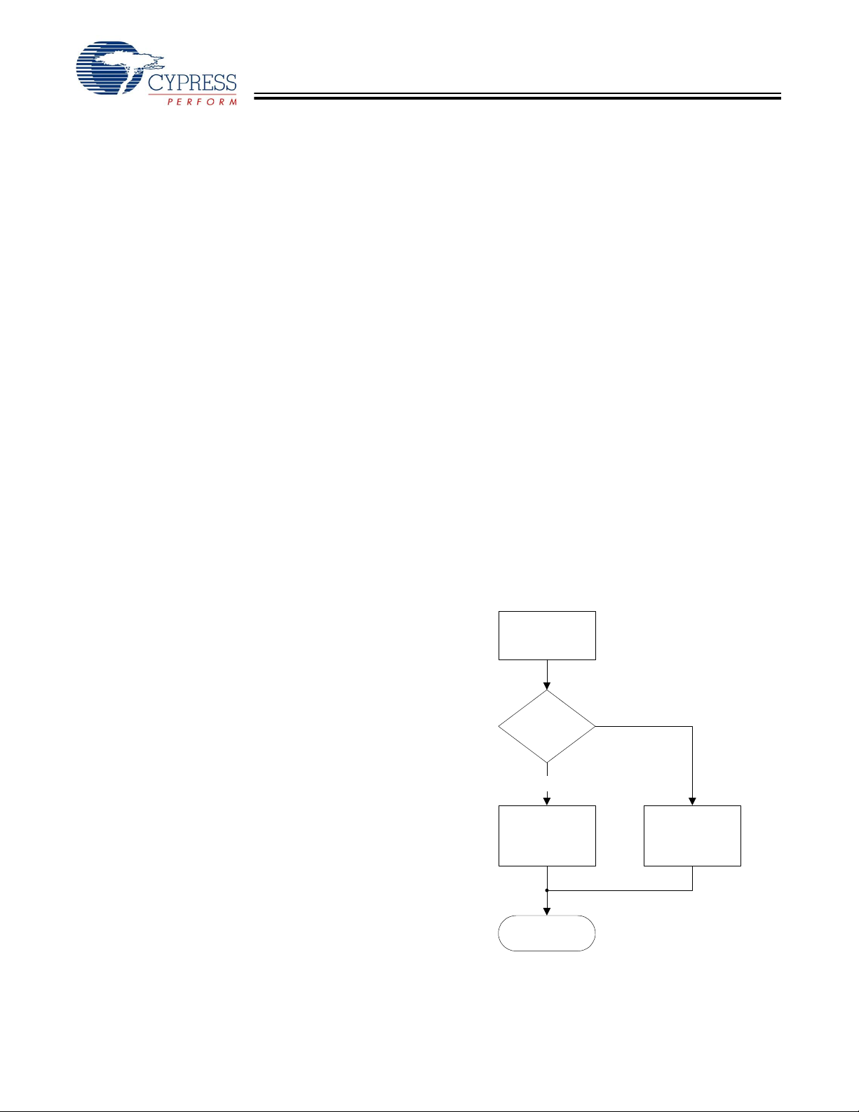
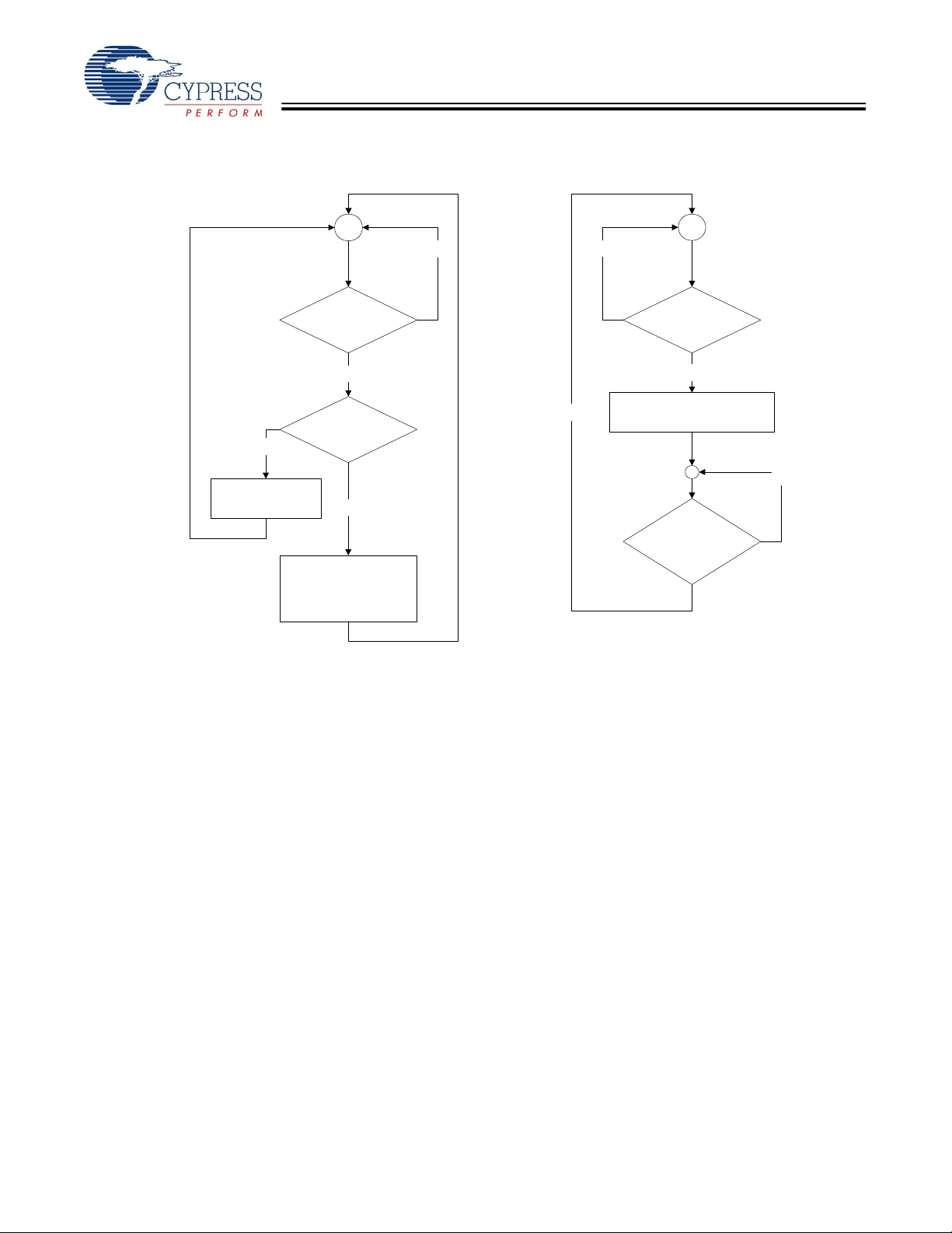
Refer to the logic flow in Figure 1 for more information on the
pinout selection process.
Most designs that use the AT2 can migrate to the AT2LP with
no changes to either the board layout or EEPROM data.
Cypress has published an application note focused on
migrating from the AT2 to the AT2LP to help expedite the
process. It can be downloaded from the Cypress website
(http://www.cypress.com) or obtained through a Cypress
representative.
Figure 1. Simplified Pinout Selection Flowchart
2
C™ bus for an
Introduction
The EZ-USB AT2LP™ (CY7C68300C/CY7C68301C and
CY7C68320C/CY7C68321C) implements a fixed-function
bridge between one USB port and one or two ATA- or
ATAPI-based mass storage device ports. This bridge adheres
to the Mass Storage Class Bulk-Only Transport Specification
(BOT) and is intended for bus- and self-powered devices.
The AT2LP is the latest addition to the Cypress USB mass
storage portfolio, and is an ideal cost- and power-reduction
path for designs that previously used Cypress’s ISD-300A1,
ISD-300LP, or EZ-USB AT2.
Specifically, the CY7C68300C/CY7C68301C includes a
mode that makes it pin-for-pin compatible with the
EZ-USB AT2 (CY7C68300A).
The USB port of the CY7C68300C/301C and
CY7C68320C/321A (AT2LP) are connected to a host
computer directly or with the downstream port of a USB hub.
Software on the USB host system issues commands and
sends data to the AT2LP and receives status and data from
the AT2LP using standard USB protocol.
The ATA/ATAPI port of the AT2LP is connected to one or two
mass storage devices. A 4 KB buffer maximizes ATA/ATAPI
Read EEPROM
EEPROM
Signature
0x4D4D?
Yes
Set
EZ-USB AT2
(CY7C68300A)
Pinout
Normal Operation
No
Set
EZ-USB AT2LP
(CY7C68300B)
Pinout
Document 001-05809 Rev. *A Page 2 of 42
[+] Feedback
Page 3
CY7C68300C/CY7C68301C
CY7C68320C/CY7C68321C
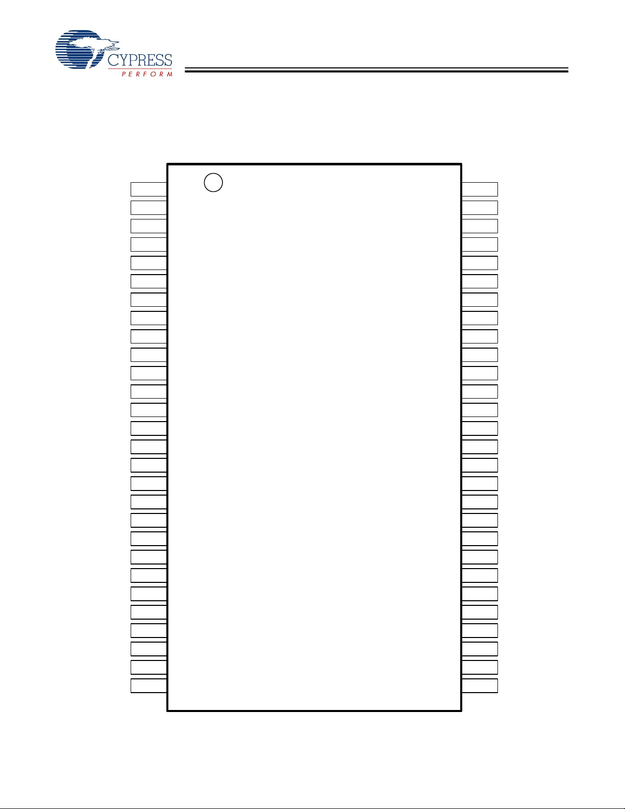
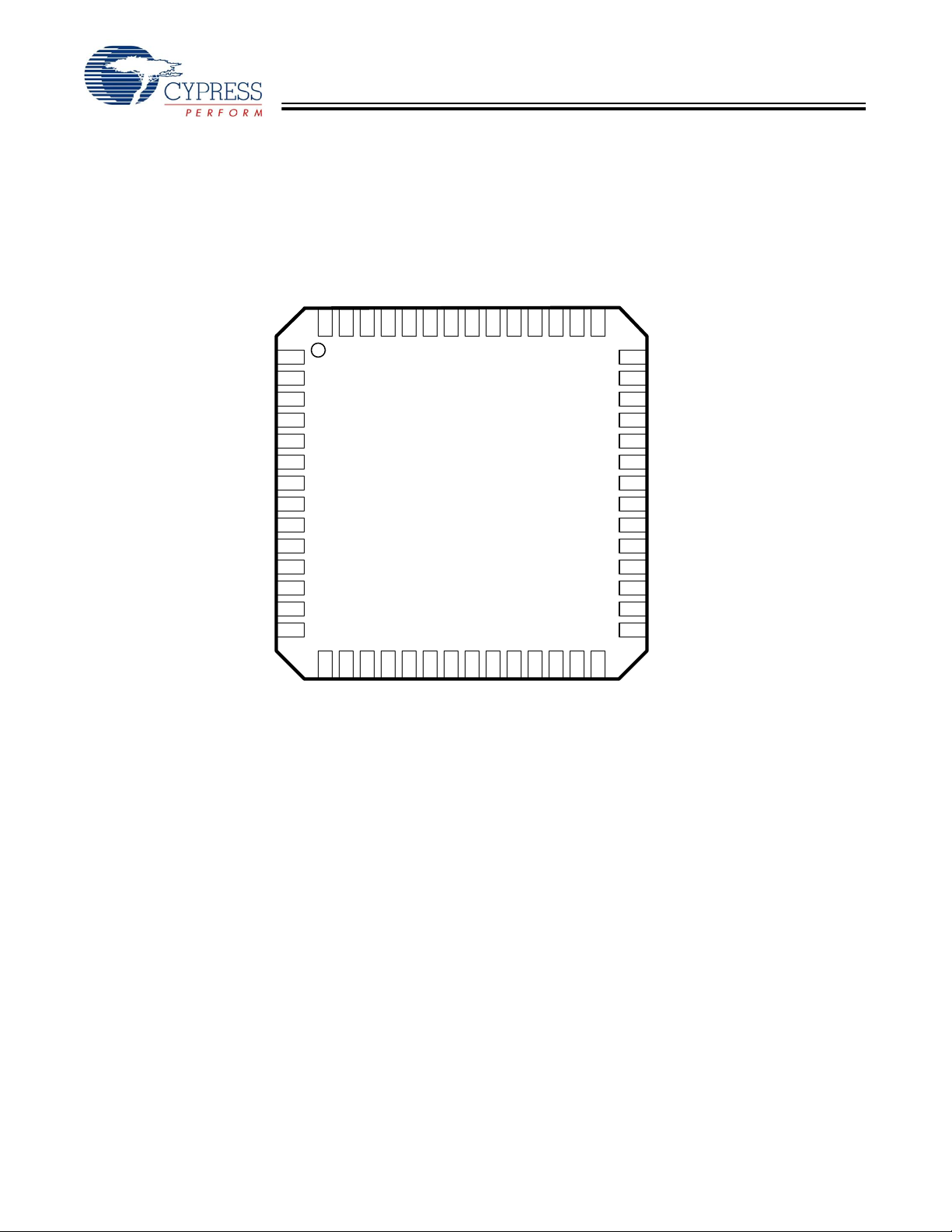
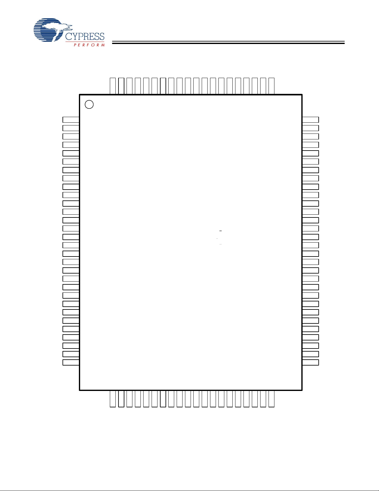
Pin Diagrams
The AT2LP is available in different package types to meet a variety of design needs. The CY7C68320C/321C is available in 56-pin
QFN and 100-pin TQFP packages to provide the greatest flexibility for new designs. The CY7C68300C/301C is available in 56-pin
SSOP and QFN package types to ensure backward compatibility with CY7C68300A designs.
Figure 2. 56-pin SSOP Pinout (CY7C68300C/CY7C68301C only)
1
DD13
2
DD14
3
DD15
4
GND
5
ATAPUEN (GND)
6
VCC
7
GND
8
IORDY
9
DMARQ
10
AVCC
11
XTALOUT
12
XTALIN
13
AGND
14
VCC
15
DPLUS
16
DMINUS
17
GND
18
VCC
19
GND
(ATA_EN) VBUS_ATA_ENABLE
(VBUS_PWR_VALID) DA2
(DA2) DRVPWRVLD
EZ-USB AT2LP
CY7C68300C
CY7C68301C
56-pin SSOP
DD12
DD11
DD10
DD9
DD8
VCC
RESET#
GND
ARESET#
CS1#
CS0#
DA1
DA0
INTRQ
VCC
DMACK#
56
55
54
53
52
51
50
49
48
47
46
45
44
43
42
41
40
39
38
20
PWR500# (PU 10K)
21
GND (Reserved)
22
SCL
23
SDA
24
VCC
25
DD0
26
DD1
27
DD2
28
DD3
Document 001-05809 Rev. *A Page 3 of 42
NOTE: Labels in italics denote pin functionality
during CY7C68300A compatibility mode.
DIOR#
DIOW#
GND
VCC
GND
DD7
DD6
DD5
DD4
37
36
35
34
33
32
31
30
29
[+] Feedback
Page 4
CY7C68300C/CY7C68301C
CY7C68320C/CY7C68321C
Figure 3. 56-pin QFN Pinout (CY7C68300C/CY7C68301C)
GND
VCC
ATAPUEN (NC)
GND
DD15
DD14
DD13
DD12
DD11
DD10
DD9
DD8
VBUS_ATA_ENABLE (ATA_EN)
VCC
IORDY
DMARQ
AVCC
XTALOUT
XTALIN
AGND
VCC
DPLUS
DMINUS
GND
VCC
GND
(PU10K) PWR500#
GND
56555453525150494847464544
1
2
3
4
5
6
7
8
9
10
11
12
NOTE: Italic labels denote pin functionality
13
14
EZ-USB AT2LP
CY7C68300C
CY7C68301C
56-pin QFN
during CY7C68300A compatibility mode.
1516171819
SCL
SDA
VCC
202122232425262728
DD0
DD1
DD2
DD3
DD4
DD5
DD6
DD7
GND
43
RESET#
42
GND
41
ARESET#
40
DA2 (VBUS_PWR_VALID)
39
CS1#
38
CS0#
37
DRVPWRVLD (DA2)
36
DA1
35
DA0
34
INTRQ
33
VCC
32
DMACK#
31
DIOR#
30
DIOW#
29
VCC
GND
Document 001-05809 Rev. *A Page 4 of 42
[+] Feedback
Page 5
CY7C68300C/CY7C68301C
CY7C68320C/CY7C68321C
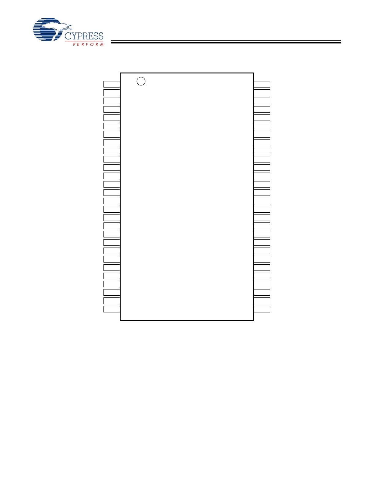
Figure 4. 56-pin SSOP Pinout (CY7C68320C/CY7C68321C)
1
2
3
4
5
6
7
8
9
10
11
12
13
14
15
16
17
18
19
20
21
22
23
24
25
26
27
28
DD13
DD14
DD15
GND
GPIO2
VCC
GND
IORDY
DMARQ
AVCC
XTALOUT
XTALIN
AGND
VCC
DPLUS
DMINUS
GND
VCC
GND
GPIO1
GND
SCL
SDA
VCC
DD0
DD1
DD2
DD3
VBUS_ATA_ENABLE
EZ-USB AT2LP
CY7C68320C
CY7C68321C
56-pin SSOP
DD12
DD11
DD10
DD9
DD8
VCC
RESET#
GND
ARESET#
DA2
CS1#
CS0#
GPIO0
DA1
DA0
INTRQ
VCC
DMACK#
DIOR#
DIOW#
GND
VCC
GND
DD7
DD6
DD5
DD4
56
55
54
53
52
51
50
49
48
47
46
45
44
43
42
41
40
39
38
37
36
35
34
33
32
31
30
29
Document 001-05809 Rev. *A Page 5 of 42
[+] Feedback
Page 6
CY7C68300C/CY7C68301C
CY7C68320C/CY7C68321C
Figure 5. 56-pin QFN Pinout (CY7C68320C/CY7C68321C)
GND
VCC
GPIO2
GND
DD15
DD14
DD13
DD12
DD11
DD10
DD9
DD8
VBUS_ATA_ENABLE
VCC
IORDY
DMARQ
AVCC
XTALOUT
XTALIN
AGND
VCC
DPLUS
DMINUS
GND
VCC
GND
GPIO1
GND
56555453525150494847464544
1
2
3
4
5
6
7
8
9
10
11
12
13
14
EZ-USB AT2LP
CY7C68320C
CY7C68321C
56-pin QFN
1516171819
SCL
SDA
VCC
202122232425262728
DD0
DD1
DD2
DD3
DD4
DD5
DD6
DD7
43
RESET#
42
GND
41
ARESET#
40
DA2
39
CS1#
38
CS0#
37
GPIO0
36
DA1
35
DA0
34
INTRQ
33
VCC
32
DMACK#
31
DIOR#
30
DIOW#
29
VCC
GND
GND
Document 001-05809 Rev. *A Page 6 of 42
[+] Feedback
Page 7
1
2
3
4
5
6
7
8
9
10
11
12
13
14
15
16
17
18
19
20
21
22
23
24
25
26
27
28
29
30
VCC
GND
IORDY
DMARQ
GND
GND
GND
GND
AVCC
XTALOUT
XTALIN
AGND
NC
NC
NC
VCC
DPLUS
DMINUS
GND
VCC
GND
SYSIRQ
GND
GND
GND
PWR500#
GND
NC
SCL
SDA
CY7C68300C/CY7C68301C
CY7C68320C/CY7C68321C
Figure 6. 100-pin TQFP Pinout (CY7C68320C/CY7C68321C only)
99989796959493929190898887868584838281
100
NC
NC
VCC
GND
DD11
DD10
VBUS_ATA_ENABLE
ATAPUEN
GND
DD15
DD14
DD13
GND
DD12
GPIO5
GPIO4
GPIO3
GPIO2
GPIO1
GPIO0
DRVPWRVLD
EZ-USB AT2LP
CY7C68320A
CY7C68321A
C
C
100-pin TQFP
VBUSPWRD
LOWPWR#
DD9
DD8
VCC
RESET#
NC
GND
ARESET#
DA2
CS1#
CS0#
DA1
DA0
INTRQ
VCC
GND
NC
NC
NC
NC
NC
NC
DMACK#
DIOR#
DIOW#
VCC
NC
NC
80
79
78
77
76
75
74
73
72
71
70
69
68
67
66
65
64
63
62
61
60
59
58
57
56
55
54
53
52
51
NCNCVCC
31323334353637383940414243444546474849
Document 001-05809 Rev. *A Page 7 of 42
DD0
DD1
DD2
DD3
VCC
GNDNCGNDNCGND
DD4
DD5
DD6
DD7
GND
VCC
GND
50
[+] Feedback
Page 8

CY7C68300C/CY7C68301C
CY7C68320C/CY7C68321C
Pin Descriptions
The following table lists the pinouts for the 56-pin SSOP , 56-pin
QFN and 100-pin TQFP package options for the AT2LP. Refer
to the “Pin Diagrams” on page 3 for differences between the
68300C/01C and 68320C/321C pinouts for the 56-pin
packages. For information on the CY7C68300A pinout, refer
to the CY7C68300A data sheet that is found in the ’EZ-USB
AT2’ folder of the CY4615C reference design kit CD.
Table 1. AT2LP Pin Descriptions
Note: (Italic pin names denote pin functionality during CY7C68300A compatibility mode)
100
TQFP
1 55 6 V
56
QFN
56
SSOP
Pin Name
CC
Pin
Type
Default State
at Startup
Pin Description
PWR VCC. Connect to 3.3V power source.
2 56 7 GND GND Ground.
3 1 8 IORDY I
4 2 9 DMARQ I
5
N/A N/A GND Ground.
[1]
[1]
Input ATA control. Apply a 1k pull up to 3.3V.
Input ATA control.
6
7
8
9 3 10 AV
CC
PWR Analog VCC. Connect to VCC through the shortest path
possible.
10 4 11 XTALOUT Xtal Xtal 24 MHz crystal output. (See “XTALIN, XTALOUT” on
page 11).
11 5 12 XTALIN Xtal Xtal 24 MHz crystal input. (See “XTALIN, XTALOUT” on
page 11).
12 6 13 AGND GND Analog ground. Connect to ground with as short a
path as possible.
13
N/A N/A NC No connect.
14
15
16 7 14 V
CC
PWR VCC. Connect to 3.3V power source.
17 8 15 DPLUS IO Hi-Z USB D+ signal (See “DPLUS, DMINUS” on page 11).
18 9 16 DMINUS IO Hi-Z USB D–signal (See “DPLUS, DMINUS” on page 11).
19 10 17 GND GND Ground.
20 11 18 V
CC
PWR VCC. Connect to 3.3V power source.
21 12 19 GND GND Ground.
22 N/A N/A SYSIRQ I Input USB interrupt request. (See “SYSIRQ” on page 12).
Active HIGH. Connect to GND if functionality is not
used.
23
N/A N/A GND GND Ground.
24
25
26
[3]
13
[3]
20 PWR500#
(PU 10K)
[2]
O bMaxPower request granted indicator. (See
“PWR500#” on page 14). Active LOW.
N/A for CY7C68320C/CY7C68321C 56-pin packages.
27 14 21 GND (RESERVED) Reserved. Tie to GND.
28 N/A N/A NC No connect.
29 15 22 SCL O Active for
several ms at
Clock signal for I2C interface. (See “SCL, SDA” on
page 11). Apply a 2.2k pu ll up resistor.
startup.
Notes
1. If byte 8, bit 4 of the EEPROM is set to ‘0’, the ATA interface pins are only active when VBUS_ATA_EN is asserted. See
page 14
2. A ‘#’ sign after the pin name indicates that it is active LOW.
.
“VBUS_ATA_ENABLE” on
Document 001-05809 Rev. *A Page 8 of 42
[+] Feedback
Page 9

CY7C68300C/CY7C68301C
CY7C68320C/CY7C68321C
Table 1. AT2LP Pin Descriptions
Note: (Italic pin names denote pin functionality during CY7C68300A compatibility mode) (continued)
100
TQFP
56
QFN
56
SSOP
Pin Name
Pin
Type
Default State
at Startup
Pin Description
30 16 23 SDA IO Data signal for I2C interface. (See “SCL, SDA” on
page 11).
Apply a 2.2k pull up resistor.
31
N/A N/A NC No connect.
32
33 17 24 V
CC
34 18 25 DD0 IO
35 19 26 DD1 IO
36 20 27 DD2 IO
37 21 28 DD3 IO
38 N/A N/A V
CC
PWR VCC. Connect to 3.3V power source.
[1]
[1]
[1]
[1]
Hi-Z ATA data bit 0.
Hi-Z ATA data bit 1.
Hi-Z ATA data bit 2.
Hi-Z ATA data bit 3.
PWR VCC. Connect to 3.3V power source.
39 N/A N/A GND GND Ground.
40 N/A N/A NC NC No connect.
41 N/A N/A GND Ground.
42 N/A N/A NC NC No connect.
43 N/A N/A GND Ground.
44 22 29 DD4 IO
45 23 30 DD5 IO
46 24 31 DD6 IO
47 25 32 DD7 IO
[1]
[1]
[1]
[1]
Hi-Z ATA data bit 4.
Hi-Z ATA data bit 5.
Hi-Z ATA data bit 6.
Hi-Z ATA data bit 7. Apply a 1k pull down to GND.
48 26 33 GND GND Ground.
49 27 34 V
CC
PWR VCC. Connect to 3.3V power source.
50 28 35 GND GND Ground.
51
N/A N/A NC NC No connect.
52
53 N/A N/A V
CC
54 29 36 DIOW#
[2]
PWR VCC. Connect to 3.3V power source.
[1]
O/Z
Driven HIGH
ATA control.
(CMOS)
55 30 37 DIOR# O/Z
[1]
Driven HIGH
ATA control.
(CMOS)
56 31 38 DMACK# O/Z
[1]
Driven HIGH
ATA control.
(CMOS)
57 N/A N/A NC NC No connect.
58 N/A N/A LOWPWR# O USB suspend indicator. (See “LOWPWR#” on
page 13).
59
N/A N/A NC NC No connect.
60
61
62 N/A N/A VBUSPWRD I Input Bus-powered mode selector. (See “VBUSPWRD” on
page 14).
63
N/A N/A NC NC No connect.
64
65 N/A N/A GND GND Ground.
66 32 39 V
CC
67 33 40 INTRQ I
PWR VCC. Connect to 3.3V power source.
[1]
Input ATA interrupt request.
Document 001-05809 Rev. *A Page 9 of 42
[+] Feedback
Page 10

CY7C68300C/CY7C68301C
CY7C68320C/CY7C68321C
Table 1. AT2LP Pin Descriptions
Note: (Italic pin names denote pin functionality during CY7C68300A compatibility mode) (continued)
100
TQFP
68 34 41 DA0 O/Z
56
QFN
56
SSOP
Pin Name
Pin
Type
[1]
Default State
at Startup
Driven HIGH
Pin Description
ATA address.
after 2 ms
delay
69 35 42 DA1 O/Z
[1]
Driven HIGH
ATA address.
after 2 ms
delay
70
[3]
36
[3]
43 DRVPWRVLD
(DA2)
I Input Device presence detect. (See “DRVPWRVLD” on
page 13). Configurable logical polarity is controlled by
EEPROM address 0x08. This pin must be pulled HIGH
if functionality is not utilized.
Alternate function. Input when the EEPROM configuration byte 8 has bit 7 set to one. The input value is
reported through EP1IN (byte 0, bit 0).
71 37 44 CS0# O/Z
[1]
Driven HIGH
ATA chip select.
after 2 ms
delay
72 38 45 CS1# O/Z
[1]
Driven HIGH
ATA chip select.
after 2 ms
delay
73 39 46 DA2
(VBUS_PWR_VALID)
O/Z
[1]
Driven HIGH
after 2 ms
ATA address.
delay
74 40 47 ARESET# O/Z
[1]
ATA reset.
75 41 48 GND GND Ground.
76 N/A N/A NC NC No connect.
77 42 49 RESET# I Input Chip reset (See “RESET#” on page 14).
78 43 50 V
CC
79 44 51 VBUS_ATA_ENABLE
(ATA_EN)
80 45 52 DD8 IO
81 46 53 DD9 IO
82 47 54 DD10 IO
83 48 55 DD11 IO
PWR VCC. Connect to 3.3V power source.
I Input VBUS detection (See “VBUS_ATA_ENABLE” on
page 14).
[1]
[1]
[1]
[1]
Hi-Z ATA data bit 8.
Hi-Z ATA data bit 9.
Hi-Z ATA data bit 10.
Hi-Z ATA data bit 11.
84 N/A N/A GND Ground.
85 N/A N/A V
86
N/A N/A NC NC No connect.
CC
PWR VCC. Connect to 3.3V power source.
87
88
89
90
91
92
93
36
13
54
[3]
N/A GPIO0
[3]
[3]
GPIO1
GPIO2
GPIO3
GPIO4
GPIO5
IO
[3]
General purpose IO pins (See “GPIO Pins” on
page 13). The GPIO pins must be tied to GND if
functionality is not used.
94 N/A N/A GND GND Ground.
95 49 56 DD12 IO
96 50 1 DD13 IO
97 51 2 DD14 IO
98 52 3 DD15 IO
[1]
[1]
[1]
[1]
Hi-Z ATA data bit 12.
Hi-Z ATA data bit 13.
Hi-Z ATA data bit 14.
Hi-Z ATA data bit 15.
99 53 4 GND GND Ground.
Document 001-05809 Rev. *A Page 10 of 42
[+] Feedback
Page 11
CY7C68300C/CY7C68301C
CY7C68320C/CY7C68321C
Table 1. AT2LP Pin Descriptions
Note: (Italic pin names denote pin functionality during CY7C68300A compatibility mode) (continued)
100
TQFP
100
56
QFN
[3]
54
56
SSOP
[3]
5 ATAPUEN
Pin Name
Pin
Default State
Type
IO Bus-powered ATA pull up voltage source (see
(NC)
Additional Pin Descriptions
The following sections provide additional pin information.
DPLUS, DMINUS
DPLUS and DMINUS are the USB signaling pins; they must
be tied to the D+ and D– pins of the USB connector. Because
they operate at high frequencies, the USB signals require
special consideration when designing the layout of the PCB.
See “General PCB Layout Recommendations For USB Mass
Storage Designs” on page 39 for PCB layout recommenda-
tions.
When RESET# is released, the assertion of the internal pull
up on D+ is gated by a combination of the state of the
VBUS_ATA_ENABLE pin, the value of configuration address
0x08 bit 0 (DRVPWRVLD Enable), and the detection of a
non-removable ATA/ATAPI drive on the IDE bus. See Table 2
for a description of this relationship.
at Startup
Pin Description
“ATAPUEN” on page 14).
Alternate function: General purpose input when the
EEPROM configuration byte 8 has bit 7 set to ‘1’. The
input value is reported through EP1IN (byte 0, bit 2).
pins must still be connected to pull up resistors. The SCL and
SDA pins are active for several milliseconds at startup.
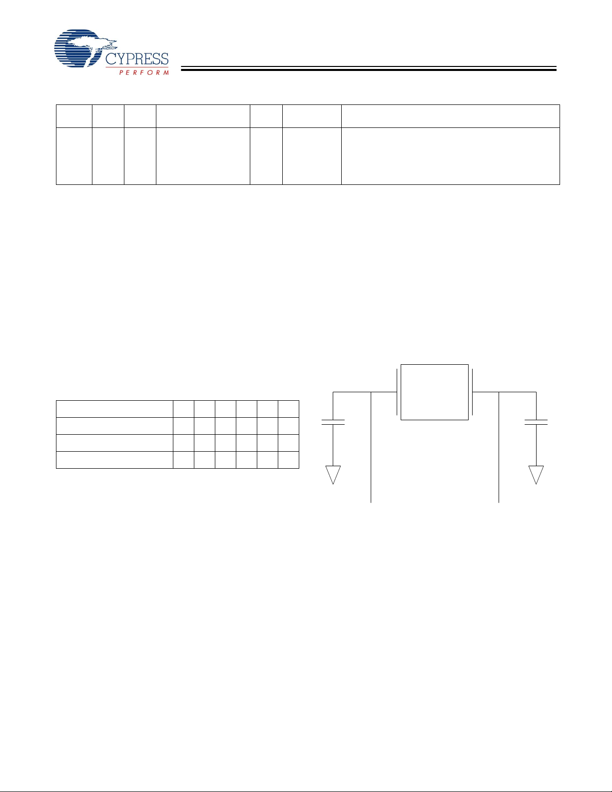
XTALIN, XTALOUT
The AT2LP requires a 24 MHz (
±100 ppm) signal to derive
internal timing. Typically, a 24 MHz (12 pF, 500 μW,
parallel-resonant, fundamental mode) crystal is used, but a 24
MHz square wave (3.3V, 50/50 duty cycle) from another
source can also be used. If a crystal is used, connect its pins
to XTALIN and XTALOUT, and also through 12 pF capacitors
to GND as shown in Figure 7. If an alternate clock source is
used, apply it to XTALIN and leave XTALOUT unconnected.
Figure 7. XTALIN/XTALOUT Diagram
Table 2. D+ Pull Up Assertion Dependencies
VBUS_ATA_EN111100
DRVPWRVLD Enable Bit110011
A TA/A TAPI Drive Detected
YesNoYesNoYesNo
State of D+ pull up111000
SCL, SDA
The clock and data pins for the I
2
C port must be connected to
the configuration EEPROM and to 2.2K pull up resistors tied
. If no EEPROM is used in the design, the SCL and SDA
to V
CC
24MHz Xtal
12pF
XTALIN XTALOUT
12pF
Document 001-05809 Rev. *A Page 11 of 42
[+] Feedback
Page 12
CY7C68300C/CY7C68301C
CY7C68320C/CY7C68321C
SYSIRQ
The SYSIRQ pin provides a way for systems to request service
from host software by using the USB Interrupt pipe on endpoint
1 (EP1). If the AT2LP has no pending interrupt data to return,
USB interrupt pipe data requests are NAKed. If pending data
is available, the AT2LP returns 16 bits of data. This data
indicates whether AT2LP is operating in high-speed or
full-speed, whether the AT2LP is reporting self-powered or
bus-powered operation, and the states of any GPIO pins that
are configured as inputs. GPIO pins can be individually set as
Table 3. Interrupt Data Bitmap
EP1 Data Byte 1 EP1 Data Byte 0
7654321076543210
RESERVED
RESERVED
RESERVED
RESERVED
RESERVED
RESERVED
USB High-Speed
inputs or outputs, with byte 0x09 of the configuration data. The
state of any GPIO pin that is not set as an input is reported as
‘0’ in the EP1 data.
Table 3 gives the bitmap for the data returned on the interrupt
pipe and Figure 8 depicts the latching algorithm incorporated
by the AT2LP .
The SYSIRQ pin must be pulled LOW if HID functionality is
used. Refer to “HID Functions for Button Controls” on page 15
for more details on HID functionality.
VBUS Powered
RESERVED
RESERVED
GPIO[5]
GPIO[4]
GPIO[3]
GPIO[2]
GPIO[1]
GPIO[0]
Document 001-05809 Rev. *A Page 12 of 42
[+] Feedback
Page 13
CY7C68300C/CY7C68301C
CY7C68320C/CY7C68321C
Figure 8. SYSIRQ Latching Algorithm
No
USB Interrupt
Pipe Polled?
Yes
Int_Data = 1?
No
NAK Request
Return Interrupt Data
Yes
Set Int_Data = 0
DRVPWRVLD
When this pin is enabled with bit 0 of configuration address
0x08 (DRVPWRVLD Enable), the A T2LP informs the host that
a removable device, such as a CF card, is present. The AT2LP
uses DRVPWRVLD to detect that the removable device is
present. Pin polarity is controlled by bit 1 of configuration
address 0x08. When DRVPWRVLD is deasserted, the AT2LP
reports a “no media present” status (ASC = 0x3A, ASQ = 0x00)
when queried by the host. When the media has been detected
again, the AT2LP reports a “media changed” status to the host
(ASC = 0x28, ASQ = 0x00) when queried.
When a removable device is used, it is always considered by
the AT2 LP to be the IDE master device. Only one removable
device may be attached to the AT2LP. If the system only
contains a removable device, bit 6 of configuration address
0x08 (Search AT A Bus) must be set to ‘0’ to disable A T A device
detection at startup. If a non-removable device is connected in
addition to a removable media device, the non-removable
device must be configured as IDE slave (device address 1).
GPIO Pins
The GPIO pins allow for a general purpose input an d output
interface. There are several different interfaces to the GPIO
pins:
• Configuration bytes 0x09 and 0x0A contain the default
settings for the GPIO pins upon initial AT2LP configuration.
No
SYSIRQ=1?
Yes
Yes
Latch State of IO Pins
Set Int_Data = 1
No
Int_Data = 0
and
SYSIRQ=0?
• The host can modify the settings of the GPIO pins during
operation. This is done with vendor-specific commands
described in “Programming the EEPROM” on page 33.
• The status of the GPIO pins is returned on the interrupt
endpoint (EP1) in response to a SYSIRQ. See “SYSIRQ”
on page 12 for SYSIRQ details.
LOWPWR#
LOWPWR# is an output pin that is driven to ‘0’ when the
AT2LP is not in suspend. LOWPWR# is placed in Hi-Z when
the AT2LP is in a suspend state. This pin only indicates the
state of the AT2LP and must not be used to determine the
status of the USB host because of variations in the behavior
of different hosts.
ATA Interface Pins
The ATA Interface pins must be connected to the corresponding pins on an IDE connector or mass storage device.
To allow sharing of the IDE bus with other master devices, the
AT2LP can place all ATA Interface Pins in a Hi-Z state
whenever VBUS_ATA_ENABLE is not asserted. Enabling this
feature is done by setting bit 4 of configuration address 0x08
to ‘1’. Otherwise, the ATA bus is driven by the AT2LP to a
default inactive state whenever VBUS_ATA_ENABLE is not
asserted.
Design practices for signal integrity as outlined in the
ATA/ATAPI-6 specification must be followed with systems that
utilize a ribbon cable interconnect between the AT2LP’s ATA
Document 001-05809 Rev. *A Page 13 of 42
[+] Feedback
Page 14

CY7C68300C/CY7C68301C
CY7C68320C/CY7C68321C
interface and the attached mass storage device, especia lly if
Ultra DMA Mode is used.
VBUS_ATA_ENABLE
VBUS_ATA_ENABLE is typically used to indicate to the
AT2LP that power is present on VBUS. This pin is polled by
the AT2LP at startup and then every 20 ms thereafter. If this
pin is ‘0’, the AT2LP releases the pull up on D+ as required by
the USB specification.
Also, if bit 4 of configuration address 0x08 is ‘1’, the ATA
interface pins are placed in a Hi-Z state when
VBUS_ATA_ENABLE is ‘0’. If bit 4 of configuration address
0x08 is ‘0’, the ATA interface pins are still driven when
VBUS_ATA_ENABLE is ‘0’.
ATAPUEN
This output can be used to control the required host pull up
resistors on the ATA interface in a bus-powered design to
minimize unnecessary power consumption when the AT2LP is
in suspend. ATAPUEN is driven to ‘0’ when the ATA bus is
inactive. ATAPUEN is driven to ‘1’ when the ATA bus is active.
ATAPUEN is set to a Hi-Z state along with all other ATA
interface pins if VBUS_ATA_ENABLE is deasserted and the
ATA_EN functionality (bit 4 of configuration address 0x08) is
enabled (0).
ATAPUEN can also be configured as a GPIO input. See “HID
Functions for Button Controls” on page 15 for more infor-
mation on HID functionality .
PWR500#
The AT2LP asserts PWR500 # to indicate that VBUS current
may be drawn up to the limit specified by the bMaxPower field
of the USB configuration descriptors. If the AT2LP enters a
low-power state, PWR500# is deasserted. When normal
operation is resumed, PWR500# is restored. The PWR500#
pin must never be used to control power sources for the
AT2LP. In the 56-pin package, PWR500# only functions during
bus-powered operation.
PWR500# can also be configured as a GPIO input. See “HID
Functions for Button Controls” on page 15 for more infor-
mation on HID functionality.
VBUSPWRD
VBUSPWRD is used to indicate self- or bus-powered
operation. Some designs require the ability to operate in either
self- or bus-powered modes. The VBUSPWRD input pin
enables these devices to switch between self-powered and
bus-powered modes by changing the contents of the
bMaxPower field and the self-powered bit in the reported
configuration descriptors (see Table 4).
Note that current USB host drivers do not poll the device for
this information, so the effect of this pin is only seen on a USB
or power on reset.
Table 4. Behavior of Descriptor Data that is Dependent Upon VBUSPWRD State
Pin VBUSPWRD = ‘1’ VBUSPWRD = ‘0’ VBUSPWRD N/A (56-pin)
bMaxPower
Reported Value
bmAttributes bit 6
Reported Value
RESET#
Asserting RESET# for 10 ms resets the entire AT2LP. In
self-powered designs, this pin is normally tied to V
a 100k resistor, and to GND through a 0.1 μF capacitor, as
shown in Figure 9.
Cypress does not recommend an RC reset circuit for
bus-powered devices because of the potential for VBUS
voltage drop, which may result in a startup time that exceeds
the USB limit. Refer to the application note titled EZ-USB
FX2™/AT2™/SX2™ Reset and Power Considerations, at
www.cypress.com, for more information.
While the AT2LP is in reset, all pins are held at their default
startup state.
0xFA
(500 mA)
‘0’
(bus-powered)
through
CC
0x01
(2 mA)
‘1’
(self-powered)
Figure 9. R/C Reset Circuit for Self-powered Designs
100KΩ
The value from configuration
address 0x34 is used.
‘0’ if bMaxPower > 0x01
‘1’ if bMaxPower ≤ 0x01
RESET#
0.1μF
Document 001-05809 Rev. *A Page 14 of 42
[+] Feedback
Page 15

CY7C68300C/CY7C68301C
CY7C68320C/CY7C68321C
HID Functions for Button Controls
Cypress’s CY7C68320C/CY7C68321C has the capability of
supporting Human Interface Device (HID) signaling to the
host.
If there is a HID descriptor in the configuration data, the GPIO
pins that are set as inputs are polled by the AT2LP logic
approximately every 17 ms (depending on other internal
interrupt routines). If a change is detected in the state of any
HID-enabled GPIO, an HID report is sent through EP1 to the
host. The report format for byte 0 and byte 1 are shown in
Table 5.
The ability to add buttons to a mass storage solution opens
new applications for data backup and other device-side notification to the host. The AT2LP Blaster soft ware, found in the
Table 5. HID Data Bitmap
USB Interrupt Data Byte 1 USB Interrupt Data Byte 0
7654321076543210
CY4615C files, provides an easy way to enable and modify the
HID features of the AT2LP.
GPIO pins can be individually set as inputs or outputs, with
byte 0x09 of the configuration data, allowing for a mix of HID
and general purpose outputs. GPIOs that are not configured
as inputs are reported with a value of ‘0’ in the HID data. The
RESERVED bits’ values must be ignored, and Cypress recommends using a bitmask in software to filter out unused HID
data.
Note that if using the 56-pin package, the reported GPIO[5:3]
values must be ignored because the pins are not actually
present.
RESERVED
RESERVED
RESERVED
RESERVED
RESERVED
RESERVED
USB High-Speed
Functional Overview
Chip functionally is described in the subsequent sections.
USB Signaling Speed
AT2LP operates at the following two rates defined in the USB
Specification Revision 2.0 dated April 27, 2000:
• Full-speed, with a signaling bit rate of 12 Mbits/sec.
• High-speed, with a signaling bit rate of 480 Mbits/sec.
AT2LP does not operate at the low-speed signaling rate of 1.5
Mbits/sec.
ATA Interface
The ATA/ATAPI port on the A T2LP is compatible with the Information Technology–AT Attachment with Packet Interface–6
(ATA/ATAPI-6) Specification, T13/1410D Rev 2a. The AT2LP
supports both ATAPI packet commands as well as ATA
commands (by use of ATA Command Blocks), as outlined in
“ATA Command Block (ATACB)” on page 15. Refer to the USB
Mass Storage Class (MSC) Bulk Only Transport (BOT) Specification for information on Command Block formatting.
VBUS Powered
RESERVED
Additionally, the AT2LP translates ATAPI SFF-8070i
commands to ATA commands for seamless integration of AT A
devices with generic Mass Storage Class BOT drivers.
ATA Command Block (ATACB)
The ATA Command Block (ATACB) functionality provides a
means of passing A TA commands and ATA register accesses
to the attached device for execution. ATACB commands are
transferred in the Command Block Wrapper Command Block
(CBWCB) portion of the Command Block Wrapper (CBW).
The ATACB is distinguished from other command blocks by
having the first two bytes of the command block match the
bVSCBSignature and bVSCBSubCommand values that are
defined in Table 6. Only command blocks that have a valid
bVSCBSignature and bVSCBSubCommand are interpreted
as ATA Command Blocks. All other fields of the CBW and
restrictions on the CBWCB remain as defined in the USB Mass
Storage Class Bulk-Only Transport Specification . The ATACB
must be 16 bytes in length. The following table and text defines
the fields of the ATACB.
RESERVED
GPIO[5]
GPIO[4]
GPIO[3]
GPIO[2]
GPIO[1]
GPIO[0]
Document 001-05809 Rev. *A Page 15 of 42
[+] Feedback
Page 16

CY7C68300C/CY7C68301C
CY7C68320C/CY7C68321C
Table 6. ATACB Field Descriptions
Byte Field Name Field Description
0 bVSCBSignature This field indicates to the CY7C68300C/CY7C68301C that the ATACB
contains a vendor-specific command block. This value of this field must match
the value in EEPROM address 0x04 for the command to be recognized as a
vendor-specific ATACB command.
1 bVSCBSubCommand This field must be set to 0x24 for ATACB commands.
2 bmA TACBActionSelect This field controls the execution of the ATACB according to the bitfield values:
Bit 7 IdentifyPacketDevice – This bit indicates that the data phase of the
command contains ATAPI (0xA1) or ATA (0xEC) IDENTIFY device data.
Setting IdentifyPacketDevice when the data phase does not contain IDENTIFY
device data results in unspecified device behavior.
0 = Data phase does not contain IDENTIFY device data
1 = Data phase contains ATAPI or ATA IDENTIFY device data
Bit 6 UDMACommand – This bit enables supported UDMA device transfers.
Setting this bit when a non-UDMA capable device is attached results in
undetermined behavior.
0 = Do not use UDMA device transfers (only use PIO mode)
1 = Use UDMA device transfers
Bit 5 DEVOverride – This bit determines whether the DEV bit value is taken
from the value assigned to the LUN during startup or from the ATACB.
0 = The DEV bit is taken from the value assigned to the LUN during startup
1 = The DEV bit is taken from the ATACB field 0x0B, bit 4
Bit 4 DErrorOverride – This bit controls the device error override feature. This
bit must not be set during a bmATACBActionSelect TaskFileRead.
0 = Data accesses are halted if a device error is detected
1 = Data accesses are not halted if a device error is detected
Bit 3 PErrorOverride – This bit controls the phase error override feature. This
bit must not be set during a bmATACBActionSelect TaskFileRead.
0 = Data accesses are halted if a phase error is detected
1 = Data accesses are not halted if a phase error is detected
Bit 2 PollAltStatOverride – This bit determines whether or not the Alternate
Status register is polled and the BSY bit is used to qualify the A TACB operation.
0 = The AltStat register is polled until BSY=0 before proceeding with the AT ACB
operation
1 = The ATACB operation is executed without polling the AltStat register.
Bit 1 DeviceSelectionOverride – This bit determines when the device selection
is performed in relation to the command register write accesses.
0 = Device selection is performed before command register write accesses
1 = Device selection is performed following command register write accesses
Bit 0 TaskFileRead – This bit determines whether or not the taskfile register
data selected in bmATACBRegisterSelect is returned. If this bit is set, the
dCBWDataTransferLength field must be set to 8.
0 = Execute ATACB command and data transfer (if any)
1 = Only read taskfile registers selected in bmAT ACBRegisterSelect and return
0x00h for all others. The format of the 8 bytes of returned data is as follows:
• Address offset 0x00 (0x3F6) – Alternate Status
• Address offset 0x01 (0x1F1) – Features/Error
• Address offset 0x02 (0x1F2) – Sector Count
• Address offset 0x03 (0x1F3) – Sector Number
• Address offset 0x04 (0x1F4) – Cylinder Low
• Address offset 0x05 (0x1F5) – Cylinder High
• Address offset 0x06 (0x1F6) – Device/Head
• Address offset 0x07 (0x1F7) – Command/Status
Document 001-05809 Rev. *A Page 16 of 42
[+] Feedback
Page 17

CY7C68300C/CY7C68301C
CY7C68320C/CY7C68321C
Table 6. ATACB Field Descriptions (continued)
Byte Field Name Field Description
3 bmATACBRegisterSelect This field controls which of the taskfile register read or write accesses occur.
4 bATACBTransferBlockCount This value indicates the maximum requested block size be in 512-byte incre-
5–12 bATACBTaskFileWriteData These bytes contain ATA register data used with ATA command or PIO write
13–15 Reserved These bytes must be set to 0x00 for ATACB commands.
T askfile read data is always 8 bytes in length, and unselected register data are
returned as 0x00. Register accesses occur in sequential order as outlined
below (0 to 7):
Bit 0 (0x3F6) Device Control/Alternate Status
Bit 1 (0x1F1) Features/Error
Bit 2 (0x1F2) Sector Count
Bit 3 (0x1F3) Sector Number
Bit 4 (0x1F4) Cylinder Low
Bit 5 (0x1F5) Cylinder High
Bit 6 (0x1F6) Device/Head
Bit 7 (0x1F7) Command/Status
ments. This value must be set to the last value used for the ’Sectors per block’
in the SET_MULTIPLE_MODE command. Legal values are 0, 1, 2, 4, 8, 16,
32, 64, and 128 where 0 indicates 256 sectors per block. A command failed
status is returned if an illegal value is used in the ATACB.
operations. Only registers selected in bmAT ACBRegisterSelect are required to
hold valid data when accessed. The registers are as follows.
ATACB Address Offset 0x05 (0x3F6) – Device Control
ATACB Address Offset 0x06 (0x1F1) – Features
ATACB Address Offset 0x07 (0x1F2) – Sector Count
ATACB Address Offset 0x08 (0x1F3) – Sector Number
ATACB Address Offset 0x09 (0x1F4) – Cylinder Low
ATACB Address Offset 0x0A (0x1F5) – Cylinder High
ATACB Address Offset 0x0B (0x1F6) – Device
ATACB Address Offset 0x0C (0x1F7) – Command
Document 001-05809 Rev. *A Page 17 of 42
[+] Feedback
Page 18

Operating Modes
The different modes of operation and EEPROM information
are presented in the following sections.
Operational Mode Selection Flow
During the power-up sequence, the AT2LP queries the I
for an EEPROM. The AT2LP then selects a pinout configuration as shown below, and checks to see if ARESET# is
configured for Board Manufacturing Test Mode.
• If no EEPROM is detected, the AT2LP uses the values in
the factory-programmable (fused) memory space. See
“Fused Memory Data” on page 19 for more information. This
Figure 10. Operational Mode Selection Flow
2
C bus
CY7C68300C/CY7C68301C
CY7C68320C/CY7C68321C
is not a valid mode of operation if no factory programming
has been done.
• If an EEPROM signature of 0x4D4D is found, the
CY7C68300C/CY7C68301C uses the same pinout and
EEPROM format as the CY7C68300A (EZ-USB AT2+).
• If an EEPROM signature of 0x534B is found, the AT2LP
uses the values stored in the EEPROM to configure the USB
descriptors for normal operation.
• If an EEPROM is detected, but an invalid signature is read,
the AT2LP defaults into Board Manufacturing Test Mode.
Check I2C Bus
Signature
0x534B?
Set
EZ-USB AT2LP
Pinout
No
VBUS_ATA_ENABLE
Pin HIGH?
Yes
ARESET#
Pin LOW?
Yes
EEPROM
Found?
Yes
Signature
0x4D4D?
YesYes
Set
EZ-USB AT2+
(CY7C68300A)
Pinout
No
Load Fused
Memory Data
(AT2LP Pinout)
No
No
DD7 Pin Set
HIGH
ARESET#
Pin HIGH?
Yes
Board Manufacturing
Test Mode
No
Normal Mass
Storage Mode
Document 001-05809 Rev. *A Page 18 of 42
[+] Feedback
Page 19

CY7C68300C/CY7C68301C
CY7C68320C/CY7C68321C
Fused Memory Data
When no EEPROM is detected at startup, the AT2LP
enumerates with the VID/PID/DID values that are stored in the
fused memory space. These values can be programmed into
the AT2LP during chip manufacturing for high volume applications to avoid the need for an external EEPROM in some
designs. Contact your local Cypress Semiconductor sales
office for more information on this feature.
If no factory programming has been done, the values returned
from the fused memory space would all be 0x00, which is not
a valid mode of operation. In this case the chip uses the
manufacturing mode and return the default descriptors
(VID/PID of 0x4B4/0x6830). An EEPROM must be used with
designs that do not use factory-programmed chips in order to
identify the device as your company’s product.
Normal Mass Storage Mode
In Normal Mass Storage Mode, the chip behaves as a USB 2.0
to ATA/ATAPI bridge. This includes all typical USB device
states (powered, configured, etc.). The USB descriptors are
returned according to the values stored in the external
EEPROM or fused memory space. A unique serial number is
required for Mass Storage Class Bulk-Only Transport
compliance, which is one reason why an EEPROM or
factory-programmed part is needed.
Board Manufacturing Test Mode
In Board Manufacturing Test Mode the AT2LP behaves as a
USB 2.0 device but the ATA/ATAPI interface is not fully active.
This mode must not be used for mass storage operation in a
finished design. In this mode, the AT2LP allows for reading
from and writing to the EEPROM, and for board level testing,
through vendor specific ATAPI commands utilizing the CBW
Command Block as described in the USB Mass Storage Class
Bulk-Only Transport Specification. There is a vendor-specific
ATAPI command for EEPROM accesses (CfgCB) and one for
board level testing (MfgCB), as described in the following
sections.
There is a convenient method available for starting the AT2LP
in Board Manufacturing Test Mode to allow reprogramming of
EEPROMs without a mass storage device attached. If the A T A
Reset (ARESET#) line is LOW on power up, the AT2LP enters
Board Manufacturing T est Mode. It is recommended that a 10k
resistor be used to pull ARESET# to LOW . An easy way to pull
the ARESET# line LOW is to short pins 1 and 3 on the 40-pin
ATA connector with a 10k resistor, that ties the ARESET# line
to the required pull down on DD7.
CfgCB
The cfg_load and cfg_read vendor-specific commands are
passed down through the bulk pipe in the CBWCB portion of
the CBW. The format of this CfgCB is shown below. Byte 0 is
a vendor-specific command designator whose value is configurable and set in the configuration data (address 0x04). Byte 1
must be set to 0x26 to identify it as a CfgCB command. Byte2
is reserved and must be set to zero. Byte 3 is used to
determine the memory source to write/read. For the AT2LP,
this byte must be set to 0x02, indicating the EEPROM is
present. Bytes 4 and 5 are used to determine the start
address, which must always be 0x0000. Bytes 6 through 15
are reserved and must be set to zero.
The data transferred to the EEPROM must be in the format
specified in Table 11 of this data sheet. Maximum data transf er
size is 255 bytes.
The data transfer length is determined by the CBW Data
Transfer Length specified in bytes 8 through 11
(dCBWDataTransferLength) of the CBW (refer to Table 7).
The type/direction of the command is determined by the
direction bit specified in byte 12, bit 7 (bmCBWFlags) of the
CBW (refer to Table 7).
Table 7. Command Block Wrapper
Bits
Offset76543210
0–3 DCBWSignature
4–7 dCBWTag
8–11 (08h–0Bh) dCBWDataTransferLength
12 (0Ch) bwCBWFLAGS
Dir Obsolete Reserved (0)
13 (0Dh) Reserved (0) bCBWLUN
14 (0Eh) Reserved (0) bCBWCBLength
15–30 (0Fh1Eh) CBWCB (CfgCB or MfgCB)
Document 001-05809 Rev. *A Page 19 of 42
[+] Feedback
Page 20

CY7C68300C/CY7C68301C
CY7C68320C/CY7C68321C
Table 8. Example CfgCB
Offset CfgCB Byte Descriptions Bits
76543210
0bVSCBSignature (set in configuration bytes) 00100100
1bVSCBSubCommand (must be 0x26) 00100110
2Reserved (must be set to zero) 00000000
3Data Source (must be set to 0x02) 00000010
4Start Address (LSB) (must be set to zero) 00000000
5Start Address (MSB) (must be set to zero) 00000000
6–15 Reserved (must be set to zero) 00000000
MfgCB
The mfg_load and mfg_read vendor-specific commands are
passed down through the bulk pipe in the CBWCB portion of
the CBW. The format of this MfgCB is shown as follows. Byte0
is a vendor-specific command designator whose value is
configurable and set in the AT2LP configuration data. Byte 1
must be 0x27 to identify a MfgCB. Bytes 2 through 15 are
reserved and must be set to zero.
The data transfer length is determined by the CBW Data
Transfer Length specified in bytes 8 through 11
(dCBWDataTransferLength) of the CBW. The type and
direction of the command is determined by the direction bit
specified in byte 12, bit 7 (bmCBWFlags) of the CBW.
Table 9. Example MfgCB
Offset MfgCB Byte Description Bits
76543210
0 0 bVSCBSignature
(set in configuration bytes)
1 1 bVSCBSubCommand
(hardcoded 0x27)
2–15 2–15 Reserved (must be zero) 0 0 0 0 0 0 0 0
Mfg_load
During a Mfg_load, the AT2LP enters into Manufacturing Test
Mode. Manufacturing Test Mode is provided as a means to
implement board or system level interconnect tests. During
Manufacturing Test Mode operation, all outputs not directly
associated with USB operation are controllable. Normal
control of the output pins are disabled. Control of the select
AT2LP IO pins and their tri-state controls are mapped to the
ATAPI data packet associated with this request. (See Table 10
for an explanation of the required Mfg_load data format.) Any
data length can be specified, but only bytes 0 through 3 are
mapped to pins, so a length of 4 bytes is recommended. To
exit Manufacturing Test Mode, a hard reset (toggle RESET#)
is required.
00100100
00100111
Mfg_read
This USB request returns a ’snapshot’ of select AT2LP input
pins. AT2LP input pins not directly associated with USB
operation can be sampled at any time during Manufacturing
Test Mode operation. See Table 10 for an explanation of the
Mfg_read data format. Any data length can be specified, but
only bytes 0 through 3 contain usable information, so a length
of 4 bytes is recommended.
Table 10.Mfg_read and Mfg_load Data Format
Byte Bits Read/Load Function
0 7 R/L ARESET#
6RDA2
5:4 R/L CS#[1:0]
3 R/L DRVPWRVLD
2:1 R/L DA[1:0]
0RINTRQ
1 7 L DD[15:0] High-Z Status
0 = Hi-Z all DD pins
1 = Drive DD pins
6RMFG_SEL
0 = Mass Storage Mode
1 = Manufacturing Mode
5 R VBUS_ATA_ENABLE
4RDMARQ
3 R IORDY
2R/LDMACK#
1R/LDIOR#
0R/LDIOW#
2 7:0 R/L DD[7:0]
3 7:0 R/L DD[15:8]
Document 001-05809 Rev. *A Page 20 of 42
[+] Feedback
Page 21

CY7C68300C/CY7C68301C
CY7C68320C/CY7C68321C
EEPROM Organization
The contents of the recommended 256-byte (2048-bit) I
EEPROM are arranged as follows. In Table 11, the column
labeled ‘Required Contents’ contains the values that must be
used for proper operation of the AT2LP. The column labeled
‘Variable Contents’ contains suggested entries and values that
may vary (like string lengths) according to the EEPROM data.
Some values, such as the Vendor ID, Product ID and device
serial number, must be customized to meet USB compliance.
The ‘AT2LP Blaster’ tool in the CY4615C kit can be used to
edit and program these values into an AT2LP-based product
(refer to Figure 11). The ‘AT2LP Primer’ tool can be used to
Figure 11. Snapshot of ‘AT2LP Blaster’ Utility
2
program AT2LP-based products in a manufacturing
environment and provides for serial number randomization.
C
See “Board Manufacturing Test Mode” on pa ge 19 for details
on how to use vendor-specific ATAPI commands to read and
program the EEPROM.
The address pins on the serial EEPROM must be set such that
the EEPROM is at physical address 2 (A0 = 0, A1 = 1, A2 = 0)
or address 4 (A0 = 0, A1 = 0, A2 = 1) for EEPROM devices
that are internally byte-addressed memories. It is recommended that the address pins be set this way even on
EEPROMs that may indicate that the address pins are internal
no-connects.
Document 001-05809 Rev. *A Page 21 of 42
[+] Feedback
Page 22

CY7C68300C/CY7C68301C
CY7C68320C/CY7C68321C
Table 11.Configuration Data Organization
Byte
Address
Note Devices running in Backward Compatibility (CY7C68300A) Mode must use the CY7C68300A EEPROM organization, and
not the format shown in this document. Refer to the CY7C68300A data sheet for the CY7C68300A EEPROM format.
AT2LP Configuration
0x00 EEPROM signature byte 0 I
0x01 EEPROM signature byte 1 I
0x02 APM Value ATA Device Automatic Power Management Value. If an
0x03 Reserved Must be set to 0x00. 0x00
0x04 bVSCBSignature Value Value in the first byte of the CBW CB field that designates
0x05 Reserved Bits 7:6 0x07
Configuration
Item Name
2
C EEPROM signature byte 0. This byte must be 0x53 for
proper AT2LP pin configuration.
2
C EEPROM signature byte 1. This byte must be 0x4B for
proper AT2LP pin configuration.
attached ATA device supports APM and this field contains
other than 0x00, the AT2LP issues a SET_FEATURES
command to Enable APM with this value during the drive
initialization process. Setting APM Value to 0x00 disables
this functionality. This value is ignored with ATAPI devices.
that the CB is to be decoded as vendor specific ATA
commands instead of the ATAPI command block. See
“Functional Overview” on page 15 for more detail on how
this byte is used.
Enable mode page 8 Bit 5
Enable the write caching mode page (page 8). If this page
is enabled, Windows disables write caching by default,
which limits write performance.
0= Disable mode page 8.
1= Enable mode page 8.
Disable wait for INTRQ Bit 4
BUSY Bit Delay Bit 3
Short Packet Before Stall Bit 2
Poll status register rather than waiting for INTRQ. Setting
this bit to 1 improves USB BOT test results but may
introduce compatibility problems with some devices.
0 = Wait for INTRQ.
1 = Poll status register instead of using INTRQ.
Enable a delay of up to 120 ms at each read of the DRQ bit
where the device data length does not match the host data
length. This allows the CY7C68300C/CY7C68301C to work
with most devices that incorrectly clear the BUSY bit before
a valid status is present.
0 = No BUSY bit delay.
1 = Use BUSY bit delay.
Determines if a short packet is sent before the STALL of an
IN endpoint. The USB Mass Storage Class Bulk-Only Speci-
fication allows a device to send a short or zero-length IN
packet before returning a STALL handshake for certain
cases. Certain host controller drivers may require a short
packet before STALL.
0 = Do not force a short packet before STALL.
1 = Force a short packet before STALL.
Configuration
Item Description
Required
Contents
0x53
0x4B
Variable
Contents
0x00
0x24
Document 001-05809 Rev. *A Page 22 of 42
[+] Feedback
Page 23

Table 11.Configuration Data Organization (co ntinued)
Byte
Address
0x06 ATA UDMA Enable B it 7
0x07 Reserved Bit s 7:3
Configuration
Item Name
SRST Enable Bit 1
Determines if the A T2LP is to do an SRST reset duri ng drive
initialization. At least one reset must be enabled. Do not set
SRST to 0 and Skip Pin Reset to 1 at the same time.
0 = Do not perform SRST during initialization.
1 = Perform SRST during initialization.
Skip Pin Reset Bit 0
Skip ARESET# assertion. When this bit is set, the AT2LP
bypasses ARESET# during any initialization other than
power up. Do not set SRST Enable to 0 and Skip Pin Reset
to 1 at the same time.
0 = Allow ARESET# assertion for all device resets.
1 = Disable ARESET# assertion except for chip reset cycles.
Enable Ultra DMA data transfer support for ATA devices. If
enabled, and if the AT A device reports UDMA support for the
indicated modes, the AT2LP uses UDMA data transfers at
the highest negotiated rate possible.
0 = Disable ATA device UDMA support.
1 = Enable ATA device UDMA support.
ATAPI UDMA Enable Bit 6
Enable Ultra DMA data transfer support for ATAPI devices.
If enabled, and if the ATAPI device reports UDMA support
for the indicated modes, the AT2LP uses UDMA data
transfers at the highest negotiated rate possible.
0 = Disable ATAPI device UDMA support.
1 = Enable ATAPI device UDMA support.
UDMA Modes Bits 5:0
These bits select which UDMA modes are enabled. The
AT2LP operates in the highest enabled UDMA mode
supported by the device. The AT2LP supports UDMA modes
2, 3, and 4 only.
Bit 5 = Reserved. Must be set to 0.
Bit 4 = Enable UDMA mode 4.
Bit 3 = Enable UDMA mode 3.
Bit 2 = Enable UDMA mode 2.
Bit 1 = Reserved. Must be set to 0.
Bit 0 = Reserved. Must be set to 0.
Must be set to 0.
Multi-word DMA mode Bit 2
This bit enables multi-word DMA support. If this bit is set and
the drive supports it, multi-word DMA is used.
PIO Modes Bits 1:0
These bits select which PIO modes are enabled. Setting to
‘1’ enables use of that mode with the attached drive, if the
drive supports it. Multiple bits may be set. The AT2LP
operates in the highest enabled PIO mode supported by the
device. The AT2LP supports PIO modes 0, 3, and 4 only.
PIO mode 0 is always enabled and has no corresponding
configuration bit.
Bit 1 = Enable PIO mode 4.
Bit 0 = Enable PIO mode 3.
Configuration
Item Description
CY7C68300C/CY7C68301C
CY7C68320C/CY7C68321C
Required
Contents
Variable
Contents
0xD4
0x07
Document 001-05809 Rev. *A Page 23 of 42
[+] Feedback
Page 24

Table 11.Configuration Data Organization (co ntinued)
Byte
Address
0x08 BUTTON_MODE Bit 7
0x09 Reserved
Configuration
Item Name
Button mode (100-pin package only). Sets ATAPUEN,
PWR500# and DRVPWRVLD to become button inputs
returned on bits 2, 1, and 0 of EP1IN. This bit must be set to
‘0’ if the 56-pin packages are used.
0 = Disable button mode.
1 = Enable button mode.
SEARCH_ATA_BUS Bit 6
Search A T A bus af ter RESET to detect non-removable A TA
and ATAPI devices. Systems with only a removable device
(like CF readers) must set this bit to ‘0’. Systems with at least
one non-removable device must set this bit to ‘1’.
0 = Do not search for ATA devices.
1 = Search for ATA devices.
BIG_PACKAGE Bit 5
ATA_EN Bit 4
Reserved Bit 3
Reserved Bit 2
Drive Power Valid Polarity Bit 1
Drive Power Valid Enable Bit 0
General Purpose IO Pin
Output Enable
Selects the 100- or 56-pin package pinout configuration.
Using the wrong pinout may result in unpredictable behavior.
0 = Use 56-pin package pinout.
1 = Use 100-pin package pinout.
Drive ATA bus when AT2LP is in suspend. For designs in
which the ATA bus is shared between the AT2LP and
another ATA master (such as an MP3 player), the AT2LP
can place the ATA interface pins in a Hi-Z state when it
enters suspend. For designs that do not share the ATA bus,
the ATA signals must be driven while the AT2LP is in
suspend to avoid floating signals.
0 = Drive ATA signals when AT2LP is in suspend.
1 = Set ATA signals to Hi-Z when AT2LP is in suspend.
Reserved. This bit must be set to ‘0’.
Reserved. This bit must be set to ‘0’
Configure the logical polarity of the DRVPWRVLD input pin.
0 = Active LOW (‘connector ground’ indication)
1 = Active HIGH (power indication from device)
Enable the DRVPWRVLD pin. When this pin is enabled, the
AT2LP enumerates a removable A TA device, like CompactFlash or MicroDrive, as the IDE master device. Enabling this
pin also affects other pins related to removable device
operation.
0 = Disable removable ATA device support.
1 = Enable removable ATA device support.
Bits 7:6
Reserved. Must be set to zero.
Bits 5:0
GPIO[5:0] Input and output control. GPIOs can be individually set as inputs or outputs using these bits.
0 = Hi-Z (pin is an input). The state of the signal connected
to GPIO input pins is reported in the SYSIRQ or HID data.
1 = Output enabled (pin is an output). The state of GPIO
output pins is controlled by the value in address 0x0A.
Configuration
Item Description
CY7C68300C/CY7C68301C
CY7C68320C/CY7C68321C
Required
Contents
Variable
Contents
0x78
0x00
Document 001-05809 Rev. *A Page 24 of 42
[+] Feedback
Page 25

CY7C68300C/CY7C68301C
CY7C68320C/CY7C68321C
Table 11.Configuration Data Organization (co ntinued)
Byte
Address
0x0A Reserved
0x0B LUN0 Identify String This byte is a pointer to the start of a 24 byte ASCII
0x0C LUN1 Identify String This byte is a pointer to the start of a 24 byte ASCII
0x0D Delay After Reset Number of 20-ms ticks to wait between AT2LP startup or
0x0E Reserved Bits 7:5
0x0F Reserved Must be set to 0x00 0x00
Device Descriptor
0x10 bLength Length of device descriptor in bytes 0x12
0x1 1 bDescriptor Type Descriptor type. 0x01
Configuration
Item Name
Bits 7:6
Reserved. Must be set to zero.
GPIO Output Pin State
Bus-Powered Flag Bit 4
CF UDMA Enable Bit 3
Fixed Number of Logical Bits 2:1
Search ATA on VBUS Bit 0
Bits 5:0
These bits select the value driven on the GPIO pins that are
configured as outputs in configuration address 0x09.
0 = Drive the GPIO pin LOW
1 = Drive the GPIO pin HIGH
(non-Unicode) string in the EEPROM that is used as the
LUN0 device identifier. This string is used by many operating
systems as the user-visible name for the drive. If this byte is
0x00, the Identify Device data from the drive is used instead.
(non-Unicode) string in the EEPROM that is used as the
LUN1 device identifier. This string is used by many operating
systems as the user-visible name for the drive. If this byte is
0x00, the Identify Device data from the drive is used instead.
reset, and the first attempt to access any drives.
Must be set to zero.
Enable bus-powered HDD support. This bit enables the use
of DRVPWRVLD features without reporting the LUN0 device
as removable media.
0 = LUN0 is removable media or DRVPWRVLD is disabled
1 = LUN0 device is bus-powered and non-removable
Enable UDMA transfers for removable devices. Some CF
devices interfere with UDMA transfers when more than one
drive is connected to the ATA bus.
0 = Do not use UDMA transfers with removable devices
(UDMA signals are not connected to the CF pins).
1 = Allow UDMA transfers to be used with removable
devices (UDMA signals are connected to the CF pins).
Assume the presence of devices and do not perform a
search of the ATA bus to discover the number of LUNs.
00 = Search ATA bus and determine number of LUNs
01 = Assume only LUN0 present; no ATA bus search
10 = Assume LUN0 and LUN1 present; no ATA bus search
11 = Assume LUN0 and LUN1 present; no ATA bus search
Search for A T A devices when VBUS returns. If this bit is set,
the ATA bus is searched for ATA devices every time
VBUS_ATA_ENABLE is asserted. This feature allows the
AT2LP to be used in designs where the drive may be physically removed (like docking stations or port replicators).
0 = Search ATA bus on VBUS_ATA_ENABLE assertion
1 = No ATA bus search on VBUS_ATA_ENABLE assertion
Configuration
Item Description
Required
Contents
Variable
Contents
0x00
0x00
0x00
0x00
0x00
Document 001-05809 Rev. *A Page 25 of 42
[+] Feedback
Page 26

CY7C68300C/CY7C68301C
CY7C68320C/CY7C68321C
Table 11.Configuration Data Organization (co ntinued)
Byte
Address
0x12 bcdUSB (LSB) USB Specification release number in BCD 0x00
0x13 bcdUSB (MSB) 0x02
0x14 bDeviceClass Device class 0x00
0x15 bDeviceSubClass Device subclass 0x00
0x16 bDeviceProtocol Device protocol 0x00
0x17 bMaxPacketSize0 USB packet size supported for default pipe 0x40
0x18 idVendor (LSB) Vendor ID. Cypress’ Vendor ID may only be used for evalu0x19 idVendor (MSB)
0x1A idProduct (LSB) Product ID Your
0x1B idProduct (MSB)
0x1C bcdDevice (LSB) Device release number in BCD LSB (product release
0x1D bcdDevice (MSB) Device release number in BCD MSB (silicon release
0x1E iManufacturer Index to manufacturer string. This entry must equal half of
0x1F iProduct Index to product string. This entry must equal half of the
0x20 iSerialNumber Index to serial number string. This entry must equal half of
0x21 bNumConfigurations Number of configurations supported
Device Qualifier
0x22 bLength Length of device descriptor in bytes 0x0A
0x23 bDescriptor Type Descriptor type 0x06
0x24 bcdUSB (LSB) USB Specification release number in BCD 0x00
0x25 bcdUSB (MSB) USB Specification release number in BCD 0x02
0x26 bDeviceClass Device class 0x00
0x27 bDeviceSubClass Device subclass 0x00
0x28 bDeviceProtocol Device protocol 0x00
0x29 bMaxPacketSize0 USB packet size supported for default pipe 0x40
0x2A bNumConfigurations Number of configurations supported 0x01
0x2B bReserved Reserved for future use. Must be set to zero 0x00
Configuration Descriptor
0x2C bLength Length of configuration descriptor in bytes 0x09
0x2D bDescriptorType Descriptor type 0x02
0x2E bT otalLength (LSB) Number of bytes returned in this configuration. This includes
0x2F bTotalLength (MSB) 0x00
0x30 bNumInterfaces Number of interfaces supported 0x01
0x31 bConfiguration Value The value to use as an argument to Set Configuration to
Configuration
Item Name
Configuration
Item Description
ation purposes, and not in released products.
number)
number)
the address value where the string starts or 0x00 if the string
does not exist.
address value where the string starts or 0x00 if the string
does not exist.
the address value where the string starts or 0x00 if the string
does not exist. The USB Mass Storage Class Bulk-Only
Tr ansport Specification requires a unique serial number (in
upper case, hexadecimal characters) for each device.
1 for mass storage: 2 for HID: 3 for CSM
the configuration descriptor plus all the interface and
endpoint descriptors.
select the configuration. This value must be set to 0x01.
Required
Contents
0x01
Variable
Contents
Your
Vendor ID
Product ID
Your
release
number
0x53
0x69
0x75
0x03
0x20
Document 001-05809 Rev. *A Page 26 of 42
[+] Feedback
Page 27

CY7C68300C/CY7C68301C
CY7C68320C/CY7C68321C
Table 11.Configuration Data Organization (co ntinued)
Byte
Address
0x32 iConfiguration Index to the configuration string. This entry must equal half
0x33 bmAttributes Device attributes for this configuration
0x34 bMaxPower Maximum power consumption for this configuration. Units
Interface and Endpoint Descriptors
Interface Descriptor
0x35 bLength Length of interface descriptor in bytes 0x09
0x36 bDescriptorType Descriptor type 0x04
0x37 bInterfaceNumber Interface number 0x00
0x38 bAlternateSetting Alternate setting 0x00
0x39 bNumEndpoints Number of endpoints 0x02
0x3A bInterfaceClass Interface class 0x08
0x3B bInterfaceSubClass Interface subclass 0x06
0x3C bInterfaceProtocol Interface protocol 0x50
0x3D iInterface Index to first interface string. This entry must equal half of
USB Bulk Out Endpoint
0x3E bLength Length of this descriptor in bytes 0x07
0x3F bDescriptorType Endpoint descriptor type 0x05
0x40 bEndpointAddress This is an Out endpoint, endpoint number 2. 0x02
0x41 bmAttributes This is a bulk endpoint. 0x02
0x42 wMaxPacketSize (LSB) Max data transfer size. To be set by speed (Full-speed
0x43 wMaxPacketSize (MSB) 0x02
0x44 bInterval High-speed interval for polling (maximum NAK rate) 0x0 0
USB Bulk In Endpoint
0x45 bLength Length of this descriptor in bytes 0x07
0x46 bDescriptorType Endpoint descriptor type 0x05
0x47 bEndpointAddress This is an In endpoint, endpoint number 6 0x86
0x48 bmAttributes This is a bulk endpoint 0x02
0x49 wMaxPacketSize (LSB) Max data transfer size. Automatically set by AT2 (Full-speed
0x4A wMaxPacketSize (MSB) 0x02
0x4B bInterval High-speed interval for polling (maximum NAK rate) 0x00
(Optional) HID Interface Descriptor
0x4C bLength Length of HID interface descriptor 0x09
0x4D bDescriptorTypes Interface descriptor type 0x04
0x4E bInterfaceNumber Number of interfaces (2) 0x02
Configuration
Item Name
Configuration
Item Description
of the address value where the string starts, or 0x00 if the
string does not exist.
Bit 7 Reserved. Must be set to 1
Bit 6 Self-powered. See Table 4 for reported value
Bit 5 Remote wakeup. Must be set to 0
Bits 4–0 Reserved. Must be set to 0
used are mA*2 (i.e., 0x31 = 98 mA, 0xF9 = 498 mA). The
value entered here is only used by the 56-pin packages and
affect the reported value of bit 6 of address 0x33 in that case.
See Table 4 on page 14 for a description of what value is
reported to the host by the AT2LP.
the address value where the string starts or 0x00 if the string
does not exist.
0x0040; High-speed 0x0200)
0x0040; High-speed 0x0200)
Required
Contents
Variable
Contents
0x00
0xC0
0x01
0x00
0x00
0x00
Document 001-05809 Rev. *A Page 27 of 42
[+] Feedback
Page 28

CY7C68300C/CY7C68301C
CY7C68320C/CY7C68321C
Table 11.Configuration Data Organization (co ntinued)
Byte
Address
0x4F bAlternateSetting Alternate setting 0x00
0x50 bNumEndpoints Number of endpoints used by this interface 0x01
0x51 bInterfaceClass Class code 0x03
0x52 bInterfaceSubClass Sub class 0x00
0x53 bInterfaceSubSubClass Sub Sub class 0x00
0x54 iInterface Index of string descriptor 0x00
USB Interrupt In Endpoint
0x5E bLength Length of this descriptor in bytes 0x07
0x5F bDescriptorType Endpoint descriptor type 0x05
0x60 bEndpointAddress This is an In endpoint, endpoint number 1 0x81
0x61 bmAttributes This is an interrupt endpoint 0x03
0x62 wMaxPacketSize (LSB) Max data transfer size 0x02
0x63 wMaxPacketSize (MSB) 0x00
0x64 bInterval Interval for polling (max. NAK rate) 0x10
(Optional) HID Descriptor
0x55 bLength Length of HID descriptor 0x09
0x56 bDescriptorType Descriptor T ype HID 0x21
0x57 bcdHID (LSB) HID Class Specification release number (1.10) 0x10
0x58 bcdHID (MSB) 0x01
0x59 bCountryCode Country Code 0x00
0x5A bNumDescriptors Number of class descriptors (1 report descriptor) 0x01
0x5B bDescriptorType Descriptor Type 0x22
0x5C wDescriptorLength (LSB) Length of HID report descriptor 0x22
0x5D wDescriptorLength (MSB) 0x00
Terminator Descriptors
0x65 Terminator 0x00
(Optional) HID Report Descriptor
0x66 Usage_Page Vendor defined 0x06
0x67 0xA0
0x68 0xFF
0x69 Usage Vendor defined 0x09
0x6A 0xA5
0x6B Collection Application 0xA1
0x6C 0x01
0x6D Usage Vendor defined 0x09
0x6E 0xA6
Input Report
0x6F Usage Vendor defined 0x09
0x70 0xA7
0x71 Logical_Minimum –128 0x15
0x72 0x80
0x73 Logical_Maximum 127 0x25
0x74 0x7F
Configuration
Item Name
Configuration
Item Description
Required
Contents
Variable
Contents
Document 001-05809 Rev. *A Page 28 of 42
[+] Feedback
Page 29

CY7C68300C/CY7C68301C
CY7C68320C/CY7C68321C
Table 11.Configuration Data Organization (co ntinued)
Byte
Address
0x75 Report_Size 8 bits 0x75
0x76 0x08
0x77 Report_Count 2 fields 0x95
0x78 0x02
0x79 Input Input (Data, Variable, Absolute) 0x81
0x7A 0x02
Output Report
0x7B Usage Usage - vendor defined 0x09
0x7C 0xA9
0x7D Logical_Minimum Logical Minimum (–128) 0x15
0x7E 0x80
0x7F Logical_Maximum Logical Maximum (127) 0x25
0x80 0x7F
0x81 Report_Size Report Size 8 bits 0x75
0x82 0x08
0x83 Report_Count Report Count 2 fields 0x95
0x84 0x02
0x85 Output Output (Data, Variable, Absolute) 0x91
0x86 0x02
0x87 End Collection 0xC0
(optional) Standard Content Security Interface Descriptor
0x88 bLength Byte length of this descriptor 0x09
0x89 bDescriptorType Interface Descriptor type 0x0D
0x8A bInterfaceNumber
0x8B bAlternateSetting Value used to select an alternate setting for the interface
0x8C bNumEndpoints Number of endpoints used by this interface (excluding
0x8D bInterfaceClass 0x0D
0x8E bInterfaceSubClass Must be set to zero 0x00
0x8F bInterfaceProtocol Must be set to zero 0x00
0x90 iInterface Index of a string descriptor that describes this Interface 0x00
Channel Descriptor
0x91 bLength Length of this descriptor in bytes 0x09
0x92 bDescriptorType Channel descriptor type 0x22
0x93 bChannelID Number of the channel, must be a zero based value that is
0x94 bmAttributes Bits7:5
Configuration
Item Name
Number of interface 0x02
Configuration
Item Description
identified in prior field
endpoint 0) that are CSM dependent
unique across the device
Reserved. Must be set to zero
Bits 4:0
Required
Contents
Variable
Contents
0x00
0x02
0x00
0x01
Document 001-05809 Rev. *A Page 29 of 42
[+] Feedback
Page 30

CY7C68300C/CY7C68301C
CY7C68320C/CY7C68321C
Table 11.Configuration Data Organization (co ntinued)
Byte
Address
0x95 bRecipient Identifier of the target recipient
0x96 bRecipientAlt alternate setting for the interface to which this channel
0x97 bRecipientLogicalUnit Recipient Logical Unit 0x00
0x98 bMethod Index of a class-specific CSM descriptor That describes one
0x99 bMethodVariant CSM Variant descriptor 0x00
CSM Descriptor
0x9A bLength Byte length of this descriptor 0x06
0x9B bDescriptorType CSM Descriptor type 0x23
0x9C bMethodID Index of a class-specific CSM descriptor that describes on
0x9D iCSMDescriptor Index of string descriptor that describes the Content Security
0x9E bcdVersion (LSB) CSM Descriptor Version number 0x10
0x9F bcsVersion (MSB) 0x02
0xA0 Terminator 0x00
USB String Descriptor–Index 0 (LANGID)
0xA1 bLength LANGID string descriptor length in bytes 0x04
0xA2 bDescriptorType Descriptor type 0x03
0xA3 LANGID (LSB) Language supported. The CY7C68300B supports one
0xA4 LANGID (MSB) 0x04
USB String Descriptor–Manufacturer
0xA5 bLength String descriptor length in bytes (including bLength) 0x2C
0xA6 bDescriptorType Descriptor type 0x03
0xA7 bString Unicode character LSB ’C’ 0x43
0xA8 bString Unicode character MSB 0x00
0xA9 bString Unicode character LSB ’y’ 0x79
0xAA bString Unicode character MSB 0x00
0xAB bString Unicode character LSB ’p’ 0x70
0xAC bString Unicode character MSB 0x00
0xAD bString Unicode character LSB ’r’ 0x72
0xAE bString Unicode character MSB 0x00
0xAF bString Unicode character LSB ’e’ 0x65
0xB0 bString Unicode character MSB 0x00
0xB1 bString Unicode character LSB ’ s’ 0x73
0xB2 bString Unicode character MSB 0x00
0xB3 bString Unicode character LSB ’ s’ 0x73
0xB4 bString Unicode character MSB 0x00
Configuration
Item Name
Configuration
Item Description
If Recipient type field of bmAttributes = 1 then
bRecipient field is the bInterfaceNumber
If Recipient type field of bmAttributes = 2 then
bRecipient field is an endpoint address, where:
D7: Direction (0 = Out, 1 = IN)
D6...D4: Reserved and set to zero
D3...D0: Endpoint number
applies
of the Content Security Methods (CSM) offered by the
device
of the Content Security Methods offered by the device
Method
LANGID value.
Required
Contents
Variable
Contents
0x00
0x00
0x01
0x01
0x00
0x09
Document 001-05809 Rev. *A Page 30 of 42
[+] Feedback
Page 31

CY7C68300C/CY7C68301C
CY7C68320C/CY7C68321C
Table 11.Configuration Data Organization (co ntinued)
Byte
Address
0xB5 bString Unicode character LSB ’ ’ 0x20
0xB6 bString Unicode character MSB 0x00
0xB7 bString Unicode character LSB ’S’ 0x53
0xB8 bString Unicode character MSB 0x00
0xB9 bString Unicode character LSB ’e’ 0x65
0xBA bString Unicode character MSB 0x00
0xBB bString Unicode character LSB ’m’ 0x6D
0xBC bString Unicode character MSB 0x00
0xBD bString Unicode character LSB ’i’ 0x69
0xBE bString Unicode character MSB 0x00
0xBF bString Unicode character LSB ’c’ 0x63
0xC0 bString Unicode character MSB 0x00
0xC1 bString Unicode character LSB ’o’ 0x6F
0xC2 bString Unicode character MSB 0x00
0xC3 bString Unicode character LSB ’n’ 0x6E
0xC4 bString Unicode character MSB 0x00
0xC5 bString Unicode character LSB ’d’ 0x64
0xC6 bString Unicode character MSB 0x00
0xC7 bString Unicode character LSB ’u’ 0x75
0xC8 bString Unicode character MSB 0x00
0xC9 bString Unicode character LSB ’c’ 0x63
0xCA bString Unicode character MSB 0x00
0xCB bString Unicode character LSB ’t’ 0x74
0xCC bString Unicode character MSB 0x00
0xCD bString Unicode character LSB ’o’ 0x6F
0xCE bString Unicode character MSB 0x00
0xCF bString Unicode character LSB ’r’ 0x72
0xD0 bString Unicode character MSB 0x00
USB String Descriptor–Product
0xD1 bLength String descriptor length in bytes (including bLength) 0x2C
0xD2 bDescriptorType Descriptor type. 0x03
0xD3 bString Unicode character LSB ’U’ 0x55
0xD4 bString Unicode character MSB 0x00
0xD5 bString Unicode character LSB ’S’ 0x53
0xD6 bString Unicode character MSB 0x00
0xD7 bString Unicode character LSB ’B’ 0x42
0xD8 bString Unicode character MSB 0x00
0xD9 bString Unicode character LSB ’2’ 0x32
0xDA bString Unicode character MSB 0x00
0xDB bString Unicode character LSB ’.’ 0x2E
0xDC bString Unicode character MSB 0x00
0xDD bString Unicode character LSB ’0’ 0x30
0xDE bString Unicode character MSB 0x00
Configuration
Item Name
Configuration
Item Description
Required
Contents
Variable
Contents
Document 001-05809 Rev. *A Page 31 of 42
[+] Feedback
Page 32

CY7C68300C/CY7C68301C
CY7C68320C/CY7C68321C
Table 11.Configuration Data Organization (co ntinued)
Byte
Address
0xDF bString Unicode character LSB ’ ’ 0x20
0xE0 bString Unicode character MSB 0x00
0xE1 bString Unicode character LSB ’D’ 0x53
0xE2 bString Unicode character MSB 0x00
0xE3 bString Unicode character LSB ’i’ 0x74
0xE4 bString Unicode character MSB 0x00
0xE5 bString Unicode character LSB ’s’ 0x6F
0xE6 bString Unicode character MSB 0x00
0xE7 bString Unicode character LSB ’k’ 0x72
0xE8 bString Unicode character MSB 0x00
USB String Descriptor–Serial Number (Note: The USB Mass Storage Class specification requires a unique serial number in
each device. If you do not provide a unique serial number, the operating system may crash. The serial number must be at least
12 characters, but some USB hosts only use the least significant 12 characters of the serial number as a unique identifier.
0xE9 bLength String descriptor length in bytes (including bLength). 0x22
0xEA bDescriptor Type Descriptor type. 0x03
0XEB bString Unicode character LSB ’1’ 0x31
0XEC bString Unicode character MSB 0x00
0XED bString Unicode character LSB ’2’ 0x32
0XEE bString Unicode character MSB 0x00
0XEF bString Unicode character LSB ’3’ 0x33
0XF0 bString Unicode character MSB 0x00
0xF1 bString Unicode character LSB ’4’ 0x34
0xF2 bString Unicode character MSB 0x00
0xF3 bString Unicode character LSB ’5’ 0x35
0xF4 bString Unicode character MSB 0x00
0xF5 bString Unicode character LSB ’6’ 0x36
0xF6 bString Unicode character MSB 0x00
0xF7 bString Unicode character LSB ’7’ 0x37
0xF8 bString Unicode character MSB 0x00
0xF9 bString Unicode character LSB ’8’ 0x38
0xFA bString Unicode character MSB 0x00
0xFB bString Unicode character LSB ’9’ 0x39
0xFC bString Unicode character MSB 0x00
0xFD bString Unicode character LSB ’0’ 0x30
0xFE bString Unicode character MSB 0x00
0xFF bString Unicode character LSB ’A’ 0x41
0Xxx bString Unicode character MSB 0x00
0Xxx bString Unicode character LSB ’B’ 0x42
0Xxx bString Unicode character MSB 0x00
Identify Device String (Note: This is not a Unicode string. It is the ASCII string returned by the device in the Identify Device
information. It is a fixed length (24 bytes). Changing this string may cause CD authoring software to incorrectly identify the device.)
0Xxx Device name byte 1 ASCII Character ’C’ 0x43
0Xxx Device name byte 2 ASCII Character ’y’ 0x79
0Xxx Device name byte 3 ASCII Character ’p’ 0x70
Configuration
Item Name
Configuration
Item Description
Required
Contents
Variable
Contents
Document 001-05809 Rev. *A Page 32 of 42
[+] Feedback
Page 33

CY7C68300C/CY7C68301C
CY7C68320C/CY7C68321C
Table 11.Configuration Data Organization (co ntinued)
Byte
Address
0Xxx Device name byte 4 ASCII Character ’r’ 0x72
0Xxx Device name byte 5 ASCII Character ’e’ 0x65
0Xxx Device name byte 6 ASCII Character ’s’ 0x73
0Xxx Device name byte 7 ASCII Character ’s’ 0x73
0Xxx Device name byte 8 ASCII Character ’ ’ 0x20
0Xxx Device name byte 9 ASCII Character ’C’ 0x43
0Xxx Device name byte 10 ASCII Character ’u’ 0x75
0Xxx Device name byte 11 ASCII Character ’s’ 0x73
0Xxx Device name byte 12 ASCII Character ’t’ 0x74
0Xxx Device name byte 13 ASCII Character ’o’ 0x6f
0Xxx Device name byte 14 ASCII Character ’m’ 0x6d
0Xxx Device name byte 15 ASCII Character ’ ’ 0x20
0Xxx Device name byte 16 ASCII Character ’N’ 0x4e
0Xxx Device name byte 17 ASCII Character ’a’ 0x61
0Xxx Device name byte 18 ASCII Character ’m’ 0x6d
0Xxx Device name byte 19 ASCII Character ’e’ 0x65
0Xxx Device name byte 20 ASCII Character ’ ’ 0x20
0Xxx Device name byte 21 ASCII Character ’L’ 0x4c
0Xxx Device name byte 22 ASCII Character ’U’ 0x55
0Xxx Device name byte 23 ASCII Character ’N’ 0x4e
0Xxx Device name byte 24 ASCII Character ’0’ 0x30
0Xxx Unused ROM Space Amount of unused ROM space varies depending on strings. 0xFF
Configuration
Item Name
Configuration
Item Description
Required
Contents
Variable
Contents
Note: More than 0X100 bytes of configuration are shown for exampl e only. The AT2 LP only supports addresses up to 0xFF.
Programming the EEPROM
There are three methods of programming the EEPROM:
• Stand-alone EEPROM programmer
• Vendor-specific USB commands, listed in Table 12
• In-system programming (for example, bed-of-nails tester)
Any vendor-specific USB write request to the Serial ROM device configuration space simultaneously update internal configuration
register values as well. If the I
nously reset (toggle RESET#) before configuration data is reloaded.
The AT 2LP supports a subset of the ’ slow mode’ specification (100 KHz) required for 24LCXXB EEPROM family device support.
Features such as ’Multi-Master,’ ’Clock Synchronization’ (the SCL pin is output only), ’10-bit addressing,’ and ’CBUS device
support’ are not supported. Vendor-specific USB commands allow the AT2LP to address up to 256 bytes of EEPROM data.
LOAD_CONFIG_DATA
This request enables writes to the AT2LP’s configuratio n data space. The wIndex field specifies the starting address and the
wLength field denotes the data length in bytes.
2
C device is programmed without vendor specific USB commands, the AT2LP must be synchro-
Document 001-05809 Rev. *A Page 33 of 42
[+] Feedback
Page 34

CY7C68300C/CY7C68301C
CY7C68320C/CY7C68321C
Legal values for wValue are as follows:
• 0x0000 Internal Config bytes, address range 0x2 – 0xF
• 0x0002 External I
Internal Config byte writes must be constrained to addresses 0x2 through 0xF, as shown in Table 12. Attempts to write outside
this address space result in undefined operation. Internal Config byte writes only overwrite AT2LP Configuration Byte registers,
the original data source (I
Table 12.EEPROM-r elated Vendor-specific Commands
Label bmRequestType bRequest wValue wIndex wLength Data
LOAD_CONFIG_DATA 0x40 0x01 0x0000 30x02 – 0x0F Data Length Configuration
READ_CONFIG_DATA 0xC0 0x02 Data Source Starting Address Data Length Configuration
READ_CONFIG_DATA
This USB request allows data retrieval from the data source specified by the wValue field. Data is retrieved beginning at the
address specified by the wIndex field (see Table 12). The wLength field denotes the length in bytes o f data requested from the
data source.
Legal values for wValue are as follows:
• 0x0000 Configuration bytes, addresses 0x0 – 0xF only
• 0x0002 External I
Illegal values for wValue result in an undefined operation. Attempted reads from an I
result in an undefined operation. Attempts to read configuration bytes with starting addresses greater than 0xF also, result in an
undefined operation.
2
C memory device
2
C memory device) remains unchanged.
2
C memory device
Data
Data
2
C memory device when none is connected
Document 001-05809 Rev. *A Page 34 of 42
[+] Feedback
Page 35

CY7C68300C/CY7C68301C
CY7C68320C/CY7C68321C
Absolute Maximum Ratings
Storage Temperature .............................................................. ... ...........................................................................–65°C to +150°C
Ambient Temperature with Power Supplied................................................................................................................0°C to +70°C
Supply Voltage to Ground Potential.............................................................................................................. ... ......–0.5 V to +4.0 V
DC Input Voltage to Any Input Pin ........................................................................................................................................ 5.25 V
DC Voltage Applied to Outputs in Hi-Z State................................................................................................. –0.5 V to V
Power Dissipation..............................................................................................................................................................300 mW
Static Disc harge Voltage................................... ................................................................................................................> 2000 V
Max Output Current Per IO Port (D0-D7, D8-15, ATA control)................. ... .. ........................................................................ 10 mA
Operating Conditions
TA (Ambient Temperature Under Bias)........................................................................................................................0°C to +70°C
Supply Voltage ..................................................................................................................... ................................+3.00V to +3.60V
Ground Voltage...........................................................................................................................................................................0V
F
(Oscillator or Crystal Frequency)................................................................................24 MHz ± 100 ppm, Parallel Resonant
osc
DC Characteristics
Parameter Description Conditions Min. Typ. Max. Unit
V
CC
V
Ramp Supply Ramp Up 0V to 3.3V 200 μs
CC
V
IH
V
IL
I
I
V
IH_X
V
IL_X
V
OH
V
OL
I
OH
I
OL
C
IN
I
SUSP
I
CC
I
UNCONFIG
T
RESET
Supply Voltage 3.00 3.3 3.60 V
Input High Voltage 2 5.25 V
Input Low Voltage –0.5 0.8 V
Input Leakage Current 0 < VIH < V
CC
±10 μA
Crystal Input HIGH Voltage 2 5.25 V
Crystal Input LOW Voltage –0.5 0.8 V
Output Voltage High I
Output Voltage Low I
= 4 mA 2.4 V
OUT
= –4 mA 0.4 V
OUT
Output Current High 4mA
Output Current Low 4mA
Input Pin Capacitance All but DPLUS/DMINUS 10 pF
DPLUS/DMINUS 15 pF
Suspend Current Connected 0.5 1.2 mA
CY7C68300C/CY7C68320C Disconnected 0.3 1.0 mA
Suspend Current Connected 300 380 μA
CY7C68301C/CY7C68321C Disconnected 100 150 μA
Supply Current USB High-Speed 50 85 mA
USB Full-Speed 35 65 mA
Unconfigured Current Current before device is granted full
43 mA
amount requested in bMaxPower
Reset Time After Valid Power VCC > 3.0V 5.0 ms
Pin Reset After Power Up 200 μs
CC
+ 0.5 V
Document 001-05809 Rev. *A Page 35 of 42
[+] Feedback
Page 36

AC Electrical Characteristics
CY7C68300C/CY7C68301C
CY7C68320C/CY7C68321C
ATA Timing Characteristics
The ATA interface supports ATA PIO modes 0, 3, and 4, Ultra
DMA modes 2, 3, and 4, and multi-word DMA mode 2, per the
ATA/ATAPI 6 Specification. The highest enabled transfer rate
common to both the AT2LP and the attached mass storage
device is used. The AT2LP automatically determines the
transfer rates during drive initialization based upon the values
in the AT2LP configuration space and the data reported by the
drives in response to an IDENTIFY DEVICE command.
USB Transceiver Characteristics
Complies with the USB 2.0 specification for full- and
high-speed modes of operation.
Ordering Information
Part Number Package Type GPIO Pins
CY7C68300C-56PVXC 56 SSOP Lead-free for self- and bus-powered designs –
CY7C68301C-56PVXC 56 SSOP Lead-free for battery-powered designs –
CY7C68300C-56LFXC 56 QFN Lead-free for self- and bus-powered designs –
CY7C68301C-56LFXC 56 QFN Lead-free for battery-powered designs –
CY7C68320C-56LFXC 56 QFN Lead-free for self- and bus-powered designs 3
CY7C68320C-56PVXC 56 SSOP Lead-free for self- and bus-powered designs 3
CY7C68321C-56LFXC 56 QFN Lead-free for battery-powered designs 3
CY7C68320C-100AXC 100 TQFP Lead-free for self- and bus-powered designs 6
CY7C68321C-100AXC 100 TQFP Lead-free for battery-powered designs 6
CY4615B EZ-USB AT2L P Reference Design Kit n/a
[4]
[4]
[4]
Note
4. The General Purpose inputs can be enabled on ATAPUEN, PWR500#, and DRVPWRVLD with EEPROM byte 8, bit 7 on CY7C68320C/CY7C68321C.
Document 001-05809 Rev. *A Page 36 of 42
[+] Feedback
Page 37

Package Diagrams
Figure 12. 100-Pin Thin Plastic Quad Flatpack (14 x 20 x 1.4 mm) A101
16.00±0.20
14.00±0.10
20.00±0.10
22.00±0.20
100
1
30
31 50
81
80
0.30±0.08
0.65
TYP.
51
CY7C68300C/CY7C68301C
CY7C68320C/CY7C68321C
1.40±0.05
12°±1°
(8X)
SEE DETAIL
0.20 MAX.
A
GAUGE PLANE
R 0.08 MIN.
0.20 MAX.
0.25
0°-7°
0.60±0.15
1.00 REF.
0° MIN.
R 0.08 MIN.
0.20 MIN.
0.20 MAX.
DETAIL
1.60 MAX.
0.10
51-85050-*B
STAND-OFF
0.05 MIN.
0.15 MAX.
SEATING PLANE
NOTE:
1. JEDEC STD REF MS-026
2. BODY LENGTH DIMENSION DOES NOT INCLUDE MOLD PROTRUSION/END FLASH
MOLD PROTRUSION/END FLASH SHALL NOT EXCEED 0.0098 in (0.25 mm) PER SIDE
BODY LENGTH DIMENSIONS ARE MAX PLASTIC BODY SIZE INCLUDING MOLD MISMATCH
3. DIMENSIONS IN MILLIMETERS
A
Document 001-05809 Rev. *A Page 37 of 42
[+] Feedback
Page 38

Package Diagrams (continued)
Figure 13. 56-lead Shrunk Small Outline Package 056
28
1
CY7C68300C/CY7C68301C
CY7C68320C/CY7C68321C
.020
0.395
0.420
0.292
0.299
DIMENSIONS IN INCHES MIN.
MAX.
0.088
0.092
29
0.720
0.730
0.025
BSC
0.008
0.0135
56
0.008
0.016
0.095
0.110
SEATING PLANE
0.110
GAUGE PLANE
.010
0.024
0°-8°
0.040
0.005
0.010
51-85062-*C
Document 001-05809 Rev. *A Page 38 of 42
[+] Feedback
Page 39

Package Diagrams (continued)
0.80[0.031]
7.70[0.303]
7.90[0.311]
A
C
1.00[0.039] MAX.
N
SEATING PLANE
N
2
0.18[0.007]
0.50[0.020]
1
1
0.08[0.003]
0.50[0.020]
0.05[0.002] MAX.
2
(4X)
C
0.24[0.009]
0.20[0.008] REF.
0.80[0.031] MAX.
PIN1 ID
0°-12°
6.45[0.254]
8.10[0.319]
7.80[0.307]
6.55[0.258]
0.45[0.018]
0.20[0.008] R.
8.10[0.319]
7.90[0.311]
7.80[0.307]
7.70[0.303]
DIA.
0.28[0.011]
0.30[0.012]
6.55[0.258]
6.45[0.254]
0.60[0.024]
N
1
2
TOP VIEW
BOTTOM VIEW
SIDE VIEW
E-PAD
(PAD SIZE VARY
BY DEVICE TYPE)
OPTION FOR CML - BOTTOM VIEW
NOTE:
DIMENSIONS ARE SAME WITH STD DWG ON UPPER RIGHT EXCEPT
FOR THE U-GROOVE ON THE PADDLE
.000
1.925
.000
2.375
2.325
R.250
(3X)
2.275
2.175
2.075
1.975
2.225
2.125
R.400
R.300
R.200
R.100
R.600
R.500
R.400
R.300
R.100
R.200
PIN #1 ID
.680
.240TYP
.680
U-GROOVE DIMENSION
E-PAD
(PAD SIZE VARY
BY DEVICE TYPE)
DIMENSIONS IN MM[INCHES] MIN.
MAX.
REFERENCE JEDEC MO-220
Figure 14. 56-Lead QFN 8 x 8 mm LF56A
CY7C68300C/CY7C68301C
CY7C68320C/CY7C68321C
General PCB Layout Recommendations For USB Mass Storage Designs
The following recommendations must be followed to ensure
reliable high-performance operation:
• Use at least a four-layer, impedance controlled board to
maintain signal quality.
• Specify specific impedance targets (ask your board vendor
what they can achieve).
• Maintain uniform trace widths and trace spacing to control
impedance.
• Minimize reflected signals by avoiding using stubs and vias.
• Connect the USB connector shell and signal ground as near
to the USB connector as possible.
• Use bypass/flyback capacitors on VBUS near the
connector.
Document 001-05809 Rev. *A Page 39 of 42
• Keep DPLUS and DMINUS trace lengths to within 2 mm of
• Maintain a solid ground plane under the DPLUS and
• Do not place vias on the DPLUS or DMINUS trace routing
• Isolate the DPLUS and DMINUS traces from all other signal
each other in length, with a preferred length of 20–30 mm.
DMINUS traces. Do not allow the plane to be split under
these traces.
51-85144 *F
for a more stable design.
traces by no less than 10 mm.
• Source for recommendations:
• EZ-USB FX2LP PCB Design Recommendations
http://www.cypress.com
• High-speed USB Platform Design Guidelines
http://www.usb.org
[+] Feedback
Page 40

Quad Flat Package No Leads (QFN) Package Design Notes
CY7C68300C/CY7C68301C
CY7C68320C/CY7C68321C
Electrical contact of the part to the Printed Circuit Board (PCB)
is made by soldering the leads on the bottom surface of the
package to the PCB. Hence, special attention is required to the
heat transfer area below the package to provide a good
thermal bond to the circuit board. A Copper (Cu) fill must be
designed into the PCB as a thermal pad under the package.
Heat is transferred from the AT2LP through the device’s metal
paddle on the bottom side of the package. Heat from here is
conducted to the PCB at the thermal pad. It is then conducted
from the thermal pad to the PCB inner ground plane by a 5 x
5 array of vias. A via is a plated through-hole in the PCB with
a finished diameter of 13 mil. The QFN’s metal die paddle must
be soldered to the PCB’s thermal pad. Solder mask is placed
on the board top side over each via to resist solder flow into
Figure 15. Cross-Section of the Area Under the QFN Package
Solder Mask
Cu Fill
PCB Material
Via hole for thermally connecting the
QFN to the circuit board ground plane.
the via. The mask on the top side also minimizes outgassing
during the solder reflow process.
For further information on this package design, refer to the
application note Surface Mount Assembly of AMKOR’s
MicroLeadFrame (MLF) Technology. The application note
provides detailed information on board mounting guideli nes,
soldering flow, rework process, etc.
Figure 15 displays a cross-sectional area underneath the
package. The cross section is of only one via. The solder paste
template needs to be designed to allow at least 50% solder
coverage. The thickness of the solder paste template must be
5 mil. It is recommended that ’No Clean,’ type 3 solder paste
is used for mounting the part. Nitrogen purge is recommended
during reflow.
0.017” dia
Cu Fill
0.013” dia
This figure only shows the top three layers of the
circuit board: Top Solder, PCB Dielectric, and
the Ground Plane
PCB Material
Figure 16 is a plot of solder mask pattern and Figure 17 displays an X-Ray image of assembly (darker areas indicate solder).
Figure 16. Plot of the Solder Mask (White Area) Figure 17. X-Ray Image of the Assembly
Other Design Considerations
Certain design considerations must be followed to ensure
proper operation of the CY7C68300C/CY7C68301C. The
following items must be taken into account when designing a
USB device with the CY7C68300C/CY7C68301C.
Proper Power Up Sequence
Power must be applied to the CY7C68300C/CY7C68301C
before, or at the same time as the ATA/ATAPI device. If power
is supplied to the drive first, the CY7C68300C/CY7C68301C
startup in an undefined state. Designs that utilize separate
power supplies for the CY7C68300C/CY7C68301C and the
A TA/ATAPI device are not recommende d.
Document 001-05809 Rev. *A Page 40 of 42
[+] Feedback
Page 41

CY7C68300C/CY7C68301C
CY7C68320C/CY7C68321C
IDE Removable Media Devices
The AT2LP does not fully support IDE removable media
devices. Changes in media state are not reported to the
operating system so users are unable to eject/reinsert media
properly. This may result in lost or corrupted data. Note that
standard ATAPI optical drives and ATA CompactFlash-type
devices are not part of this group.
Devices With Small Buffers
The size of the drive’s buffer can greatly affect the overall data
transfer performance. Care must be taken to ensure that
Disclaimers, Trademarks, and Copyrights
Purchase of I2C™ components from Cypress or one of its sublicensed Associated Companies conveys a license under the Philips
2
I
C Patent Rights to use these components in an I2C system provided that the system conforms to the I2C Standard S pecification
as defined by Philips. Microsoft and Windows are registered trademarks of Microsoft Corporation. Apple and Mac OS are registered
trademarks of Apple Computer, Inc. EZ-USB A T2LP, EZ-USB AT2, EZ-USB FX2 and EZ-USB TX2 are trademarks, and EZ-USB
is a registered trademark of Cypress Semiconductor Corporation. All p roduct a nd company names men tioned in this d ocument
are the trademarks of their respective holders.
drives have large enough buffers to handle the flow of data to
and from it. The exact buffer size needed depends on a
number of variables, but a good rule of thumb is:
(aprox min buffer) = (data rate) * (seek time + rotation time + other)
where ’other’ may include things like the time required to
switch heads, power up a laser, etc. Drives with buffers that
are too small to handle the extra data may perform considerably slower than expected.
Document 001-05809 Rev. *A Page 41 of 42
© Cypress Semiconductor Corporation, 2006. The information contained herein is subject to change without notice. Cy press Semiconductor Corporation assumes no responsibility for the use
of any circuitry other than circuitry embodied in a Cypress product. Nor does it convey or imply any license under patent or other rights. Cypress products are not warranted nor intended to be
used for medical, life support, life saving, critical control or safety applications, unless pursuant to an express written agreement with Cypress. Furthermore, Cypress do es not authori ze its
products for use as critical components in life-support systems where a malfunction or failure may reasonably be expected to result in sign ificant injury to the us er. The inclusion of Cypress
products in life-support systems application implies that the manufacturer assumes all risk of such use and in doing so indemnifies Cypress against all charges.
[+] Feedback
Page 42

CY7C68300C/CY7C68301C
CY7C68320C/CY7C68321C
Document History Paged
Description Title: CY7C68300C/CY7C68301C/CY7C68320C/CY7C68321C EZ-USB AT2LP™ USB 2.0 to ATA/ATAPI
Bridge
Document Number: 001-05809
REV. ECN NO. Issue Date
** 409321 See ECN GIR New data sheet.
*A 611658 See ECN ARI/KKU Implemented new template. Added part number CY7C68320C-56PVXC to
Orig. of
Change
Description of Change
the Ordering Information. Corrected part numbers on figure 5 and 6. Moved
figure titles to the top of each figure per new template requirements. Made
grammatical corrections. Changed the Fused Memory Data section. Added
new figure: 56-pin SSOP (CY7C68320C/CY7C68321C).
Changed figure 10 to reflect actual Flow for Operational Mode. Changes
made between “VBUS_ATA_ENABLE PIN HIGH?” and “Board Manufacturing Test Mode”. Formatted “0=”, “1=” lines in Configuration Data Organization to always show up in the same order. Re-worded 3rd bullet point in
the Operation Selection Flow section.
GPIO2_nHS function removed and corrected the sense of ATA_EN to allow
drive on ‘0’ and Hi-Z on ‘1’.
Document 001-05809 Rev. *A Page 42 of 42
[+] Feedback
 Loading...