

CY7C68300B/CY7C68301B
CY7C68320/CY7C68321
EZ-USB AT2LP™ USB 2.0 to ATA/ATAPI Bridge
1.0 Features (CY7C68300B/CY7C68301B and
CY7C68320/CY7C68321)
• Fixed-funct ion mass st orage devi ce—requires no firmware
code
• Two power modes: Self-powered and USB bus-powered to
enable bus powered CF readers and truly portabl e USB
hard drives
• Certified co mpliant for USB 2.0 ( TI D# 40460273 ), t he USB
Mass Storage Class, and the USB Mass Storage Cl ass
Bulk-Only Transport (BO T) Specification
• Operates at high (4 80-Mbps) or full (12 -Mbps) speed USB
• Complies with ATA/ATAPI-6 specif ication
• Supports 48-bit addressing fo r large hard drives
• Supports ATA security features
• Supports al l ATA commands via ATACB function
• Supports mode page 5 for BIOS boot support
• Supports A T API serial number VPD p age retrieval for Digi tal
Rights Management (DRM) compatibility
• Supports PIO modes 0, 3, 4, multiword DM A mo de 2, and
UDMA modes 2, 3, 4
• Uses one external serial EEPROM for storage of USB
descriptor s and device configuration data
• ATA interface IRQ signal support
• Support for one or two ATA/ATAPI devices
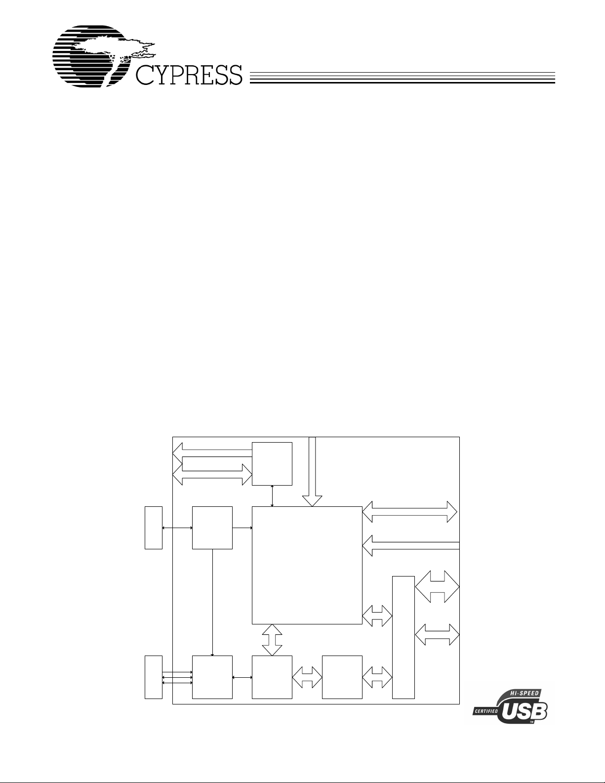
2.0 Block Diagram
• Support for Compact Flash and one ATA/ATAPI device
• Can place the ATA interface in high-impedance (Hi-Z) t o
allow sharing of the ATA bus with anothe r cont roller (e.g.,
an IEEE-1394 to ATA bridge chip or MP3 Decoder)
• Support for board-le vel manufacturing tes t vi a USB
interface
• Low-power 3.3V operation
• Fully compati ble with native USB mass storage class driver s
• Cypress mass s torage cl ass dri vers avai labl e for Windo ws
(98SE, ME, 2000, XP) and Mac OS X
1.1 Features (CY7C68320/CY7C68321 only)
• Supports HID interface or c ustom GPIOs to en able feature s
such as single butto n backup, power-off, L ED-based notification, etc.
• Lead-free 56-pin QF N and 100-pi n TQ FP packages
• CY7C68321 is ideal for bat tery-powered designs
• CY7C68320 is ideal for sel f- and bus-powered designs
1.2 Features (CY7C68300B/CY7C68301B only)
• Pin-compatible with CY7C68300A ( using Backward
Compat ibility mode)
• Lead-free 56-pin SSOP and 56-pi n Q FN packages
• CY7C68301B is ideal for bat tery-powered designs
• CY7C68300B is ideal for sel f- and bus-powered designs
24
MHz
XTAL
VBUS
D+
D-
SCL
SDA
PLL
USB 2.0 XCVR
I2C B us Controller
RESET
Internal Control Logic
CY Smar t US B
FS/HS Engine
4kByt e FIFO
Figure 2-1. Block Diagram
Control
Dat a
A
T
M isc control si gnal s
_
E
N
A
(
A
T
A
n
I
ATA
Interf ace
Logic
f
t
a
c
e
r
e
3
ATA Interf ace
Contro l Signals
16 Bit ATA Data
s
a
t
t
-
e
)
Cypress Semiconductor Corporation • 3901 North First Street • San Jose, CA 95134 • 408-943-2600
Document 38-08033 Rev. *C Revised February 14, 2005

CY7C68300B/CY7C68301B
CY7C68320/CY7C68321
3.0 Applications
The CY7C68300B/301B and CY7C68320/321 implement a
USB 2.0 bridge for all ATA/ATAPI-6 compliant mass storage
devices, such as the following.
• Hard drives
• CD-ROM, CD-R/W
• DVD-ROM, DVD-RAM, DVD+/–R/W
• MP3 players
• Personal media players
• CompactFlash
• Microdrives
• Tape drives
• Personal video recorders
The CY7C68300B/301 B and CY7C68320/321 support one or
two devices in the following configurations.
• ATA/ATAPI master only
• ATA/ATAPI slave only
• ATA/ATAPI master and slave
• CompactFl ash only
• A TA/ATAPI slave and CompactFlas h or ot her removable
IDE mast e r
3.1 Additional Resources
• CY4615B EZ-USB AT2LP Reference Design Kit
• USB Specification version 2.0
• ATA Specification T13/1410D Rev 3B
• USB Mass Storage Cl ass Bulk Only Transport Specification,
www.usb.org
4.0 Introduction
The EZ-USB AT2LP (CY7C68300B/CY7C68301B and
CY7C68320/CY7C68321) implements a fixed function bridge
between one USB port and one or two ATA- or ATAPI-based
mass storage device ports. This bridge adheres to the Mass
Storage Class Bulk-Only Transport Specification and is
intended for bus- and self-powered devices .
The AT2LP is the latest addition to t he Cypress USB mass
storage portfolio, and is an ideal cost - and power- reduct ion
path for designs that previously used the ISD-300A1, ISD300LP, or EZ-USB AT2.
Specifically, the CY7C68300B/CY7C68301B includes a
mode that makes it pin-for-pin compatible with the EZUSB AT2 (CY7C68300A).
The USB port of the CY7C68300B/30 1B and CY7C68320/321
(AT2LP) are connect ed to a host computer directly or via the
downstream port of a USB hub. Host software issues
commands and data to the AT2LP and receives status and
data from the AT2LP using standard USB protocol.
The ATA/ATAPI port of the AT2LP is connected to one or two
mass storage devi ces. A 4- Kbyte buf fer maximi zes A T A/ A T API
data transfer rates by minimizing losses due to device seek
times. The ATA i nter face s upport s A TA PIO modes 0, 3, a nd 4 ,
multiword DMA mode 2 and Ultra DMA modes 2, 3, and 4.
The device initialization process is configurable, enabling the
AT2LP to initialize ATA/ATAPI devices without software intervention.
5.0 68300A Compatibility
The CY7C68300B/301B a nd CY7 C68320/ 321 ar e avail able i n
three package t ypes that ar e pictured i n the followi ng sections .
As mentioned above, the CY7C68300B/301B contains a
backward compatibility mode that allows the
CY7C68300B/301B to be used in existing EZ-USB AT2
(CY7C68300A) designs. Please refer to the logic flow below
for more information on the pinout selection process.
Read EEPROM
EEPROM
Signature
0x4D4D?
Yes
Set
EZ-USB AT2
(CY7C68300A)
Pinout
Normal Operation
Figure 5-1. Simplifi ed Startup Flowchart (68300B only)
Document 38-08033 Rev. *C Page 2 of 36
No
Set
EZ-USB AT2LP
(CY7C68300B)
Pinout
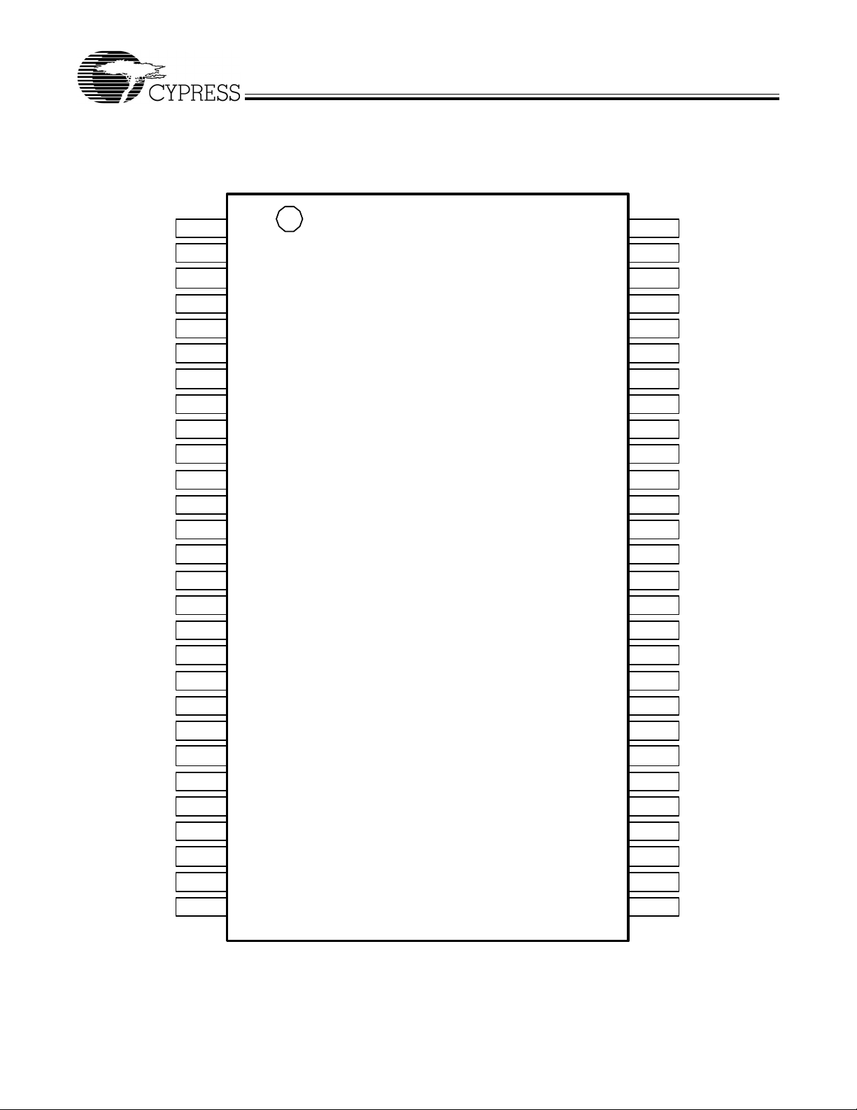
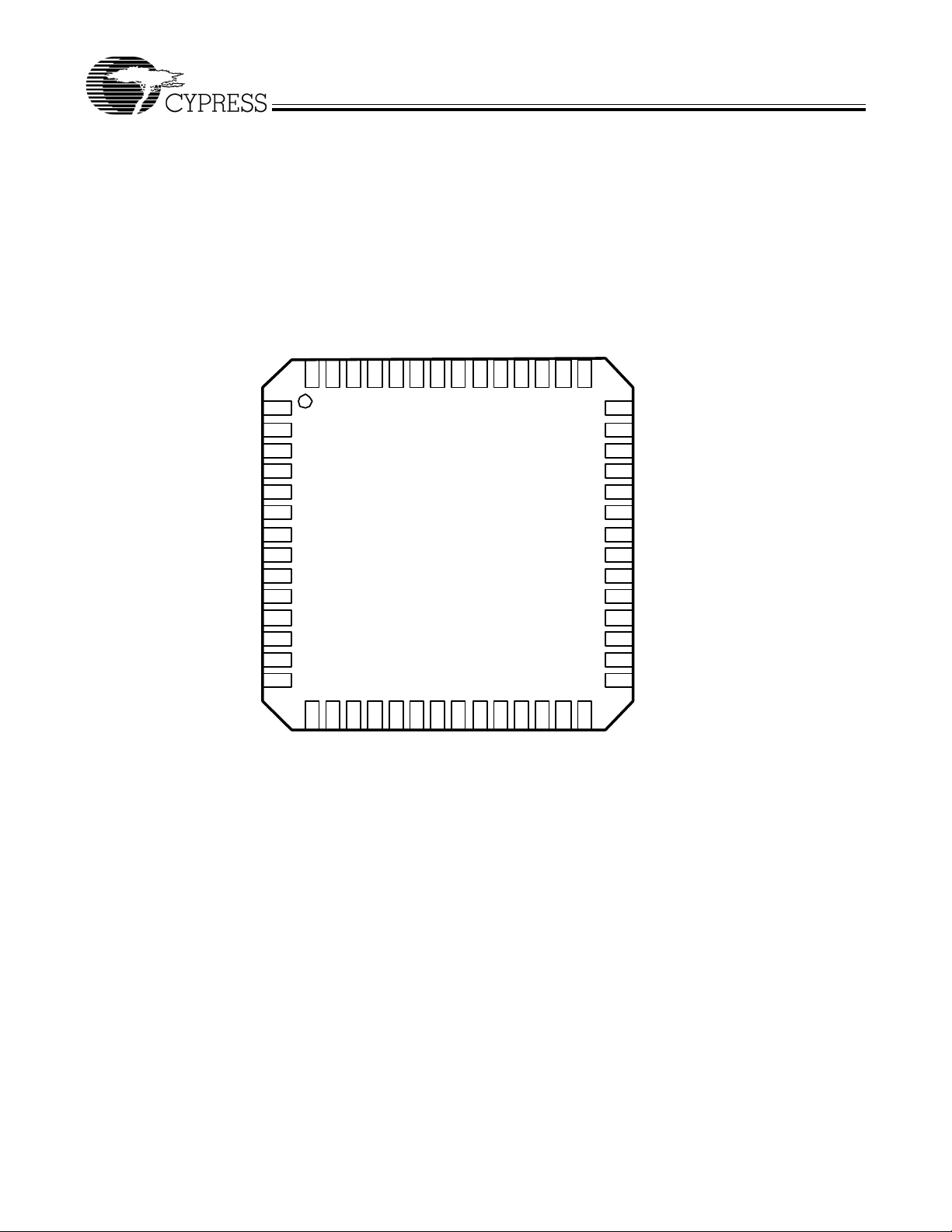
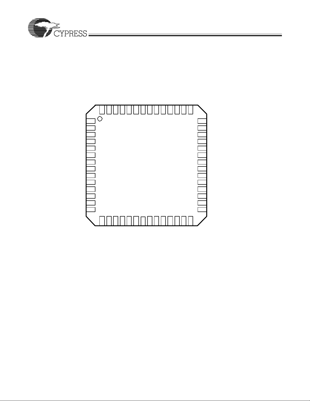
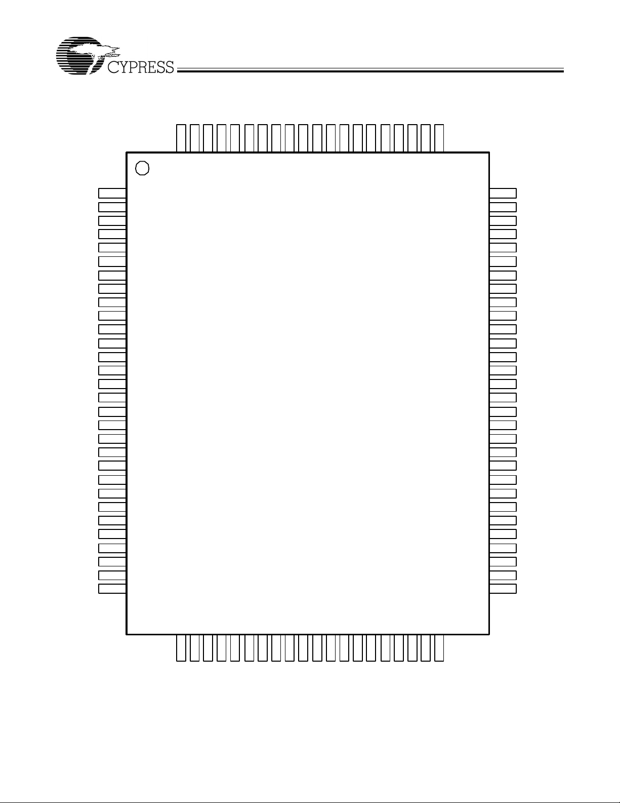
5.1 Pin Diagrams
CY7C68300B/CY7C68301B
CY7C68320/CY7C68321
1
DD13
2
DD14
3
DD15
4
GND
5
ATAPUEN (GND)
6
VCC
7
GND
8
IORDY
9
DMARQ
10
AVCC
11
XTALOUT
12
XTALIN
13
AGND
14
VCC
15
DPLUS
16
DMINUS
17
GND
18
VCC
19
GND
20
PWR500# ( PU 10K )
21
GND (Reserved)
(ATA_EN) V BUS_A TA _ENABLE
(VBUS_PWR_VALID ) DA2
(DA2) DRVPWRVLD
EZ-USB AT2LP
CY7C68300B
CY7C68301B
56-pin SSOP
DD12
DD11
DD10
DD9
DD8
VCC
RESET#
GND
ARESET#
CS1#
CS0#
DA1
DA0
INTRQ
VCC
DMACK#
DIOR#
DIOW#
56
55
54
53
52
51
50
49
48
47
46
45
44
43
42
41
40
39
38
37
36
22
SCL
23
SDA
24
VCC
25
DD0
26
DD1
27
DD2
28
DD3
Figure 5-2. 56-pin SSOP Pinout (CY7C6 8300B/CY7C68301B only)
Document 38-08033 Rev. *C Page 3 of 36
NOTE: Labels in italics denote pin functionality
during CY7C68300A compatibility mode.
GND
VCC
GND
DD7
DD6
DD5
DD4
35
34
33
32
31
30
29
GND
VCC
ATA PUE N (NC)
GND
DD15
DD14
DD13
DD12
DD11
DD10
DD9
DD8
VBUS_ATA_ENABLE (ATA_EN)
56555453525150494847464544
CY7C68300B/CY7C68301B
CY7C68320/CY7C68321
VCC
43
IORDY
DMARQ
AVCC
XTALOUT
XTALI N
AGND
VCC
DPL US
DMI NUS
GND
VCC
GND
(PU 10K) PWR500#
GND
RESET#
1
2
3
4
5
6
7
8
9
10
11
12
13
14
EZ-USB AT2LP
CY7C68300B
CY7C68301B
56-pin QFN
NOTE: Italic labels denote pin functionality
during CY7C68300A compatibility mode.
15161718192021222324252627
SCL
DD0
DD1
DD2
DD3
SDA
VCC
DD4
DD5
DD6
DD7
GND
42
GND
41
ARESET#
40
DA2 ( VBUS_PWR_VALID)
39
CS1#
38
CS0#
37
DRVPWRVLD (DA2)
36
DA1
35
DA0
34
INT RQ
33
VCC
32
DMACK#
31
DIOR#
30
DIOW#
29
28
VCC
GND
Figure 5-3. 56-pin QFN Pinout (CY7C68300B/CY7C68301B)
Document 38-08033 Rev. *C Page 4 of 36
GND
VCC
GPIO2
GND
DD15
DD14
DD13
DD12
DD11
DD10
DD9
DD8
VBUS_ATA_ENABLE
56555453525150494847464544
CY7C68300B/CY7C68301B
CY7C68320/CY7C68321
VCC
43
IORDY
DMAR Q
AVCC
XTALOUT
XTALI N
AGND
VCC
DP LUS
DM INUS
GND
VCC
GND
GPIO1
GND
1
2
3
4
5
6
7
8
9
10
11
12
13
14
EZ-USB AT2LP
CY7C68320
CY7C68321
56-pin QFN
15161718192021222324252627
SCL
DD0
DD1
DD2
DD3
SDA
VCC
DD4
DD5
DD6
DD7
GND
42
41
40
39
38
37
36
35
34
33
32
31
30
29
28
VCC
GND
Figure 5-4. 56-pin QFN Pinout (CY7 C68320/CY7C68321)
RESET#
GND
ARESET#
DA2
CS1#
CS0#
GPIO0
DA1
DA0
INT RQ
VCC
DMACK#
DIOR#
DIOW#
Document 38-08033 Rev. *C Page 5 of 36
1
2
3
4
5
6
7
8
9
10
11
12
13
14
15
16
17
18
19
20
21
22
23
24
25
26
27
28
29
30
VCC
GND
IORDY
DMARQ
GND
GND
GND
GND
AVCC
XTALOUT
XTALIN
AGND
NC
NC
NC
VCC
DPLUS
DMINUS
GND
VCC
GND
SYSIRQ
GND
GND
GND
PWR500#
GND
NC
SCL
SDA
CY7C68300B/CY7C68301B
CY7C68320/CY7C68321
99989796959493929190898887868584838281
100
NC
NC
GND
DD15
DD14
GND
DD13
DD12
GPIO5
GPIO4
GPIO3
GPIO2
GPIO1
GPIO0
ATAPUEN
VCC
GND
VBUS_ATA_ENABLE
EZ-USB AT2LP
CY7C68320B
CY7C68321B
100-pin T QFP
DD9
DD11
DD10
RESET#
ARESET#
DRVPWRVLD
INTRQ
VBUSPWRD
LOWPWR#
DMACK#
DIOR#
DIOW#
DD8
VCC
NC
GND
DA2
CS1#
CS0#
DA1
DA0
VCC
GND
NC
NC
NC
NC
NC
NC
VCC
NC
NC
80
79
78
77
76
75
74
73
72
71
70
69
68
67
66
65
64
63
62
61
60
59
58
57
56
55
54
53
52
51
NCNCVCC
31323334353637383940414243444546474849
Figure 5-5. 100-pin TQFP Pinout (CY7C68320/CY7C68321 only)
Document 38-08033 Rev. *C Page 6 of 36
DD0
DD1
DD2
DD3
VCC
GNDNCGND
NC
GND
DD4
DD5
DD6
DD7
GND
VCC
GND
50
CY7C68300B/CY7C68301B
CY7C68320/CY7C68321
5.2 Pin Descriptions
The following table lists the pinouts for the 56-pin SSOP, 56pin QFN and 100-pin TQFP package options for the AT2LP.
Please refer to the Pin Diagrams in section for differences
between the 68300B/01B and 68320/321 pinouts for the 56pin packages. For information on the CY7C68300A pinout,
please refer to the CY7C6 8300A data sheet that is foun d in the
“EZ-USB A T2” fol der of the CY4615 B refe rence d esign ki t CD.
T able 5-1. AT2LP Pin Descriptions
Note: (Italics pin names denote pin functionality during CY7C68300A-co mp atibility mode)
56
SSOP
56
QFN
100
TQFP Pin N ame
Pin
Type
1 50 96 DD13 I/O
2 51 97 DD14 I/O
3 52 98 DD15 I/O
Default St ate
at Start-up Pin Description
[1]
[1]
[1]
Hi-Z ATA Data bi t 13.
Hi-Z ATA Data bi t 14.
Hi-Z ATA Data bi t 15.
4 53 99 GND GND Ground.
5 54
[3]
100
[3]
ATAPUEN
(NC)
I/O ATA pull-up voltage source for bus-powered applica-
tions (see section 5.3.10).
Alternate Function: Input when the EEPROM config-
uration byte 8 has bit 7 set to one. The input value is
reported through EP1IN (byte 0, bit 2).
6 55 1 V
CC
PWR VCC. Connect to 3.3V power source.
7 56 2 GND GND Ground.
8 1 3 IORDY I
9 2 4 DMARQ I
N/A N/A 5
GND Ground.
[1]
[1]
Input ATA Control.
Input ATA Control.
6
7
8
10 3 9 AV
CC
PWR Anal og VCC. Connect to VCC through the shortest p ath
possible.
11 4 10 XTALOUT Xtal Xtal 24-MHz Crystal Output (see section ).
12 5 11 XTALIN Xtal Xtal 24-MHz Crystal Input (see section ).
13 6 12 AGND GND Analog Ground. Connect to ground with as shor t a
path as possi b l e .
N/A N/A 13
NC No Connect.
14
15
14 7 16 V
CC
PWR VCC. Connect to 3.3V power source.
15 8 17 DPLUS I/O Hi-Z USB D+ Signal (see section 5.3.1).
16 9 18 DMINUS I/O Hi-Z USB D– Signal (see section 5.3.1).
17 10 19 GND GND Gr ound.
18 11 20 V
CC
PWR VCC. Connect to 3.3V power source.
19 12 21 GND GND Gr ound.
N/A N/A 22 SYSIRQ I Input Active HIGH. USB interrup t req uest (see section
5.3.4). T ie to GND if functionali ty i s not used.
N/A N/A 23
GND GND Ground.
24
25
20 13
[3]
26
[3]
PWR500#
(PU 10K)
[2]
I/O Active LOW. VBUS power granted indicator used in
bus-powered designs (see section 5.3. 11).
Alternate Function for 68320.
21 14 27 GND (RESER VE D ) Reserved. Tie to GND.
Notes:
1. If byte 8, bit 4 of the EEPROM is set to ‘0’, the ATA interface pins are only active when VBUS_ATA_EN is asserted. See section 5.3.9.
2. A ‘#’ sign after the pin name indicates that it is active LOW.
3. The General Purpose inputs can be enabled on ATAPUEN, PWR500#, and DRVPWRVLD via EEPROM byte 8, bit 7 on CY7C68320/CY7C68321.
Document 38-08033 Rev. *C Page 7 of 36
CY7C68300B/CY7C68301B
CY7C68320/CY7C68321
T able 5-1. AT2LP Pin Descriptions
Note: (Italics pin names denote pin functionality during CY7C68300A-co mp atibility mode) (continued)
56
SSOP
N/A N/A 28 NC No Connect.
22 15 29 SCL O Active for
23 16 30 SDA I/O Data signal for I2C interface (see section 5.3.2).
N/A N/A 31
24 17 33 V
25 18 34 DD0 I/O
26 19 35 DD1 I/O
27 20 36 DD2 I/O
28 21 37 DD3 I/O
N/A N/A 38 V
N/A N/A 39 GND GND Ground.
N/A N/A 40 NC NC No Connect.
N/A N/A 41 GND Ground.
N/A N/A 42 NC NC No Connect.
N/A N/A 43 GND Ground.
29 22 44 DD4 I/O
30 23 45 DD5 I/O
31 24 46 DD6 I/O
32 25 47 DD7 I/O
33 26 48 GND GND Gr ound.
34 27 49 V
35 28 50 GND GND Gr ound.
N/A N/A 51
N/A N/A 53 V
36 29 54 DIOW#
37 30 55 DIOR# O/Z
38 31 56 DMACK# O/Z
N/A N/A 57 NC NC No Connect.
N/A N/A 58 LOWPWR# O USB suspend indicator (see section 5.3.7).
N/A N/A 59
N/A N/A 62 VBUSPWRD I Input Bus-powered operation selector. U s ed in sy st e m s
N/A N/A 63
N/A N/A 65 GND GND Ground.
56
QFN
100
TQFP Pin N ame
NC No Connect.
32
CC
CC
CC
NC NC No Connect.
52
CC
[2]
NC NC No Connect.
60
61
NC NC No Connect.
64
Pin
Default St ate
Type
at Start-up Pin Description
Clock signal for I2C interface (s ee section 5.3.2).
several ms at
start-up.
PWR VCC. Connect to 3.3V power source.
[1]
[1]
[1]
[1]
Hi-Z ATA Data bit 0.
Hi-Z ATA Data bit 1.
Hi-Z ATA Data bit 2.
Hi-Z ATA Data bit 3.
PWR VCC. Connect to 3.3V power source.
[1]
[1]
[1]
[1]
Hi-Z ATA Data bit 4.
Hi-Z ATA Data bit 5.
Hi-Z ATA Data bit 6.
Hi-Z ATA Data bit 7.
PWR VCC. Connect to 3.3V power source.
PWR VCC. Connect to 3.3V power source.
[1]
O/Z
Driven HIGH
ATA Control.
(CMOS)
[1]
Driven HIGH
ATA Control.
(CMOS)
[1]
Driven HIGH
ATA Control.
(CMOS)
‘0’ = Chip active. VBUS power draw gover ned by
PWR500# pin.
‘Hi-Z’ = Chip s uspen d. VBUS system cu rr ent li mited to
USB suspend mode value.
that are capabl e of bei ng bus or self-powered to
indicate the current power mode.
Document 38-08033 Rev. *C Page 8 of 36

CY7C68300B/CY7C68301B
CY7C68320/CY7C68321
T able 5-1. AT2LP Pin Descriptions
Note: (Italics pin names denote pin functionality during CY7C68300A-co mp atibility mode) (continued)
56
SSOP
39 32 66 V
40 33 67 INTRQ I
41 34 68 DA0 O/Z
42 35 69 DA1 O/Z
43 36
44 37 71 CS0# O/Z
45 38 72 CS1# O/Z
46 39 73 DA2
47 40 74 ARESET# O/Z
48 41 75 GND GND Gr ound.
N/A N/A 76 NC NC No Connect.
49 42 77 RESET# I Input Chip Reset (see section 5.3.13). This pin is normally
50 43 78 V
51 44 79 VBUS_ATA_ENABLE
52 45 80 DD8 I/O
53 46 81 DD9 I/O
54 47 82 DD10 I/O
55 48 83 DD11 I/O
N/A N/A 84 GND Ground.
N/A N/A 85 V
N/A N/A 86
N/A 36
N/A N/A 94 GND GND Ground.
56 49 95 DD12 I/O
56
QFN
[3]
[3]
[3]
13
[3]
54
100
TQFP Pin N ame
CC
[3]
70
DRVPWRVLD
(DA2)
(VBUS_PWR_VALID)
CC
(ATA_EN)
CC
NC NC No Connect.
87
88
89
90
91
92
93
GPIO0
GPIO1
GPIO2_nHS
GPIO3
GPIO4
GPIO5
Pin
Default St ate
Type
at Start-up Pin Description
PWR VCC. Connect to 3.3V power source.
[1]
[1]
Input ATA Interrupt request.
Driven HIGH
ATA Address.
after 2 ms
delay
[1]
Driven HIGH
ATA Address.
after 2 ms
delay
I Input Device Presence Detect (see section 5.3.5). Config-
urable polarity, controlled by EEPROM address 0x08.
This pin must be connect ed to GND if functionality is
not utilized.
Alternate Function: Input when the EEPROM configuration byte 8 has bit 7 set to one. The input value is
reported through EP1IN (byte 0, bit 0).
[1]
Driven HIGH
ATA Chip Select.
after 2 ms
delay
[1]
Driven HIGH
ATA Chip Select.
after 2 ms
delay
[1]
O/Z
Driven HIGH
ATA Address.
after 2 ms
delay
[1]
ATA Reset.
tied to V
through a 0.1-µF capac itor , supplying a 10-ms reset.
through a 100K resistor, and to GND
CC
PWR VCC. Connect to 3.3V power source.
I Input VBUS detection (see section 5.3.9). Indicates to the
CY7C68300B/CY7C68301B that VBUS power is
present.
[1]
[1]
[1]
[1]
Hi-Z ATA Data bit 8.
Hi-Z ATA Data bit 9.
Hi-Z ATA Data bi t 10.
Hi-Z ATA Data bit 11.
PWR VCC. Connect to 3.3V power source.
[3]
I/O
General purpose I/O pins (see section 5.3.6). The
GPIO pins must be tied to GND if funct ionality is not
utilized. If the hs_indicator conf ig bit is set, the
GPIO2_nHS pin will reflect the operating speed:
‘1’ = full-speed operation.
‘0’ = high-speed operation.
[1]
Hi-Z ATA Data bi t 12.
Document 38-08033 Rev. *C Page 9 of 36
CY7C68300B/CY7C68301B
CY7C68320/CY7C68321
5.3 Additional Pin Descriptions
5.3.1 DPLUS, DMINUS
DPLUS and DMINUS a re the USB signal ing pins; they should
be tied to the D+ and D– pins of the USB connector. Because
they operate at high frequencies, the USB signals require
special consideration when designing the layout of the PCB.
See section 15.0 for PCB layout recommendations. When
RESET# is released, the internal pull-up on D+ is controlled
by VBUS_ATA_ENABLE. When VBUS_ATA_ENABLE is
HIGH, D+ is pulled up.
5.3.2 SCL, SDA
The clock and data pins for the I
to the con figuration EEPROM and to 2 .2K pull -up resi stors t ied
to V
. The SCL and SDA pins are active for several milli-
CC
seconds at start-up.
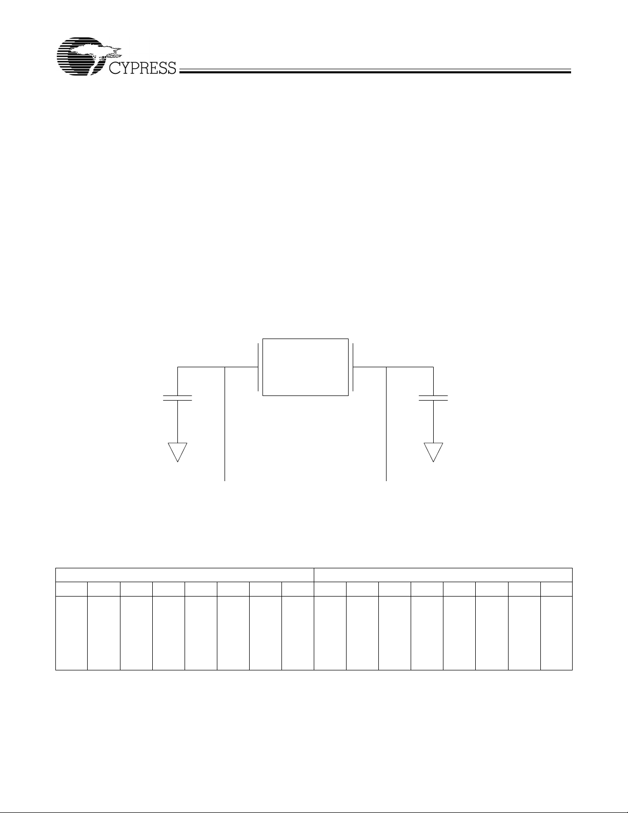
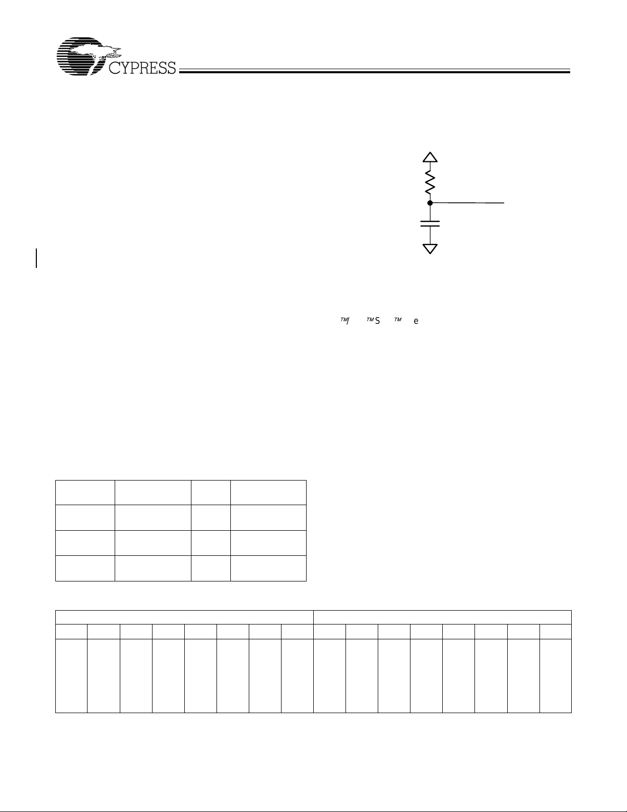
5.3.3 XTALIN, XTALOUT
The AT2LP requires a 24-MHz (
internal timing. Typically, a 24-MHz (20-pF, 500-µW, pa r a ll e l -
2
C port should be connected
±100ppm) signal to derive
24MHz Xtal
12pF
resonant fundamental mode) crystal is used, but a 24-MHz
square wave fr om another source can also be used. If a cryst al
is used, connect its pins to XTALIN and XTALOUT, and also
through 12-pF capac itors to GND as shown in Figure 5-6 . If an
alternate clock source is used, apply it to XTALIN and leave
XTALOUT open.
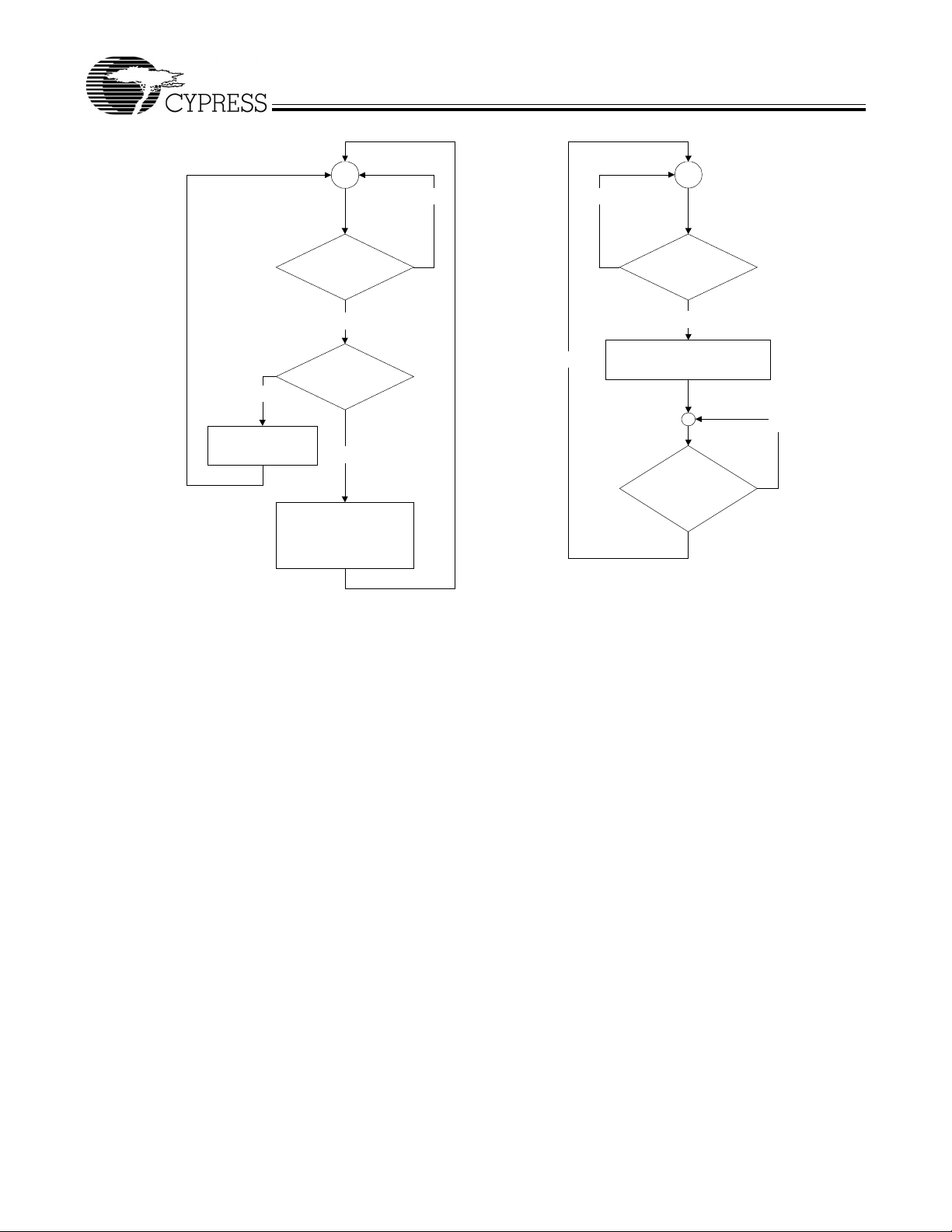
5.3.4 SYSI RQ
The SYSIRQ pin provides a way for systems to request service
from host software by using the USB Interrupt pipe. If the
AT2LP has no pending interrupt data to return, USB interrupt
pipe data req uests are NAKed. If pend ing data is a vailable , the
AT2LP returns 16 bits of data; this data indicates the
HS_MODE signal (that indicates whether AT2LP is operating
in high-speed or full-speed), the VBUSPWRD pin, and the
GPIO pin s . Table 5-2 gives the bi tmap for the data retur ned on
the interrupt pipe and Figur e 5 -7 depict s the latching algorithm
incorporated by AT2LP.
The SYSIRQ pin must be tied low if the HID function is used
(refer to Section 6.0).
12pF
XTALIN XTALOUT
Figure 5-6. XTALIN / XTALOUT Diagram
T able 5-2. USB Interrupt Pipe Data Bitmap
USB Interrupt Data Byte 1 USB Interrupt Data Byte 0
7654321076543210
RESERVED
Document 38-08033 Rev. *C Page 10 of 36
RESERVED
RESERVED
RESERVED
RESERVED
RESERVED
USB High-Speed
VBUSPWRD
RESERVED
RESERVED
GPIO[5]
GPIO[4]
GPIO[3]
GPIO[2]
GPIO[1]
GPIO[0]
CY7C68300B/CY7C68301B
CY7C68320/CY7C68321
No
USB Inte rrupt
Pipe Polled?
Yes
Int_Data = 1?
No
NAK Request
Return I n te rrupt Data
Yes
Set Int_Data = 0
Figure 5-7. SYSIRQ Latching Algorithm
5.3.5 DRVPWRVLD
When this pin is enable d via EEPROM byte 8, bit 0, the A T2 LP
will inform the host that a removable device, such as a CF
card, is present. The CY7C68300B/CY7C68301B will use
DRVPWRVLD to det ect that the removabl e device is present.
Pin polarit y is co ntrol led b y b it 1 of EEPROM addr ess 8. When
DRVPWRVLD is deasserted, the AT2LP will report a “no
media present” status ( ASC = 0x3A, ASQ = 0x00) to the host.
When the media has been detected again, the AT2LP will
report a “media changed” status to the host (ASC = 0x28,
ASQ = 0x00).
When a removable device is used, it is always the master
device. Only one removable device may be attached to the
AT2LP. If the system only contains a removable device,
EEPROM byte 8, bit 6 must be set to ‘0’ to dis able ATA device
detection at start-up. If a non-removable device is connected
in addition t o a remov able medi a devic e, it must be conf igure d
as a slave (device address 1).
DRVPWRVLD can also be configured as an input. See
Section 6.0 HID Functions fo r Button Controls.
5.3.6 GPIO Pins
The GPIO pins allow for a general purpose Input/Output
interface. There are several different interfaces to the GPIO
pins:
• Configuration bytes 0x09 and 0x0A cont a in the defaul t se ttings for the GPIO pins.
• The host can modify the settings of the GPIO pin s during
operation. This is done with vendor-spec ific commands described in Section 8.6.
No
SYSIRQ=1?
Yes
Yes
• The status of the GPIO pins is also ret urned on the interru pt
endpoint (EP1 ) i n response to a SYSIRQ. See section for
Latch State of IO Pins
Set Int_Data = 1
No
Int_Data = 0
and
SYSIRQ=0?
SYSIRQ details.
GPIO2_nHS also has an alter nate function. I f the “HS Indicator
Enable” configuration (bit 2 of EEPROM address 8) is set, the
GPIO2_nHS pin will reflect the operating speed of the device
(full- or high-speed USB).
5.3.7 LOWPWR#
LOWPWR# is an output pin that is driven to ‘0’ when the
AT 2LP is active. LOW PWR# is placed in Hi- Z when the A T2LP
is in a suspend state.
5.3.8 AT A Interface Pins
Design practices for signal integrity as outlined in the
ATA/ATAPI-6 Specification should be followed with systems
that utilize a ribbon cable interconnect between the
CY7C68300B/CY7C68301B’s ATA interface and the attached
ATA/ATAPI device, especially if Ul tr a DMA Mode is uti li zed.
5.3.9 VBUS_ATA_ENABLE
VBUS_ATA_ENABLE is typically used to indicate to the
AT2LP that power is present on VBUS. This pin is polled by
the AT2LP at start-up and then every 20ms thereafter. If this
pin is ‘1’, the inter nal 1.5K pull-up is att ached to D+. If this pin
is ‘0’, th e AT2LP will rel e as e th e pull-up on D+ as re quired by
the USB specification. Also, If EEPROM byte 8, bit 4 is ‘0’, t he
ATA interface pins will be placed in a hi gh impedance (Hi-Z)
state when VBUS_ATA_ENABLE is ‘0’. If EEPROM byte 8, bit
4 is ‘1’, the ATA interface pins will still be driven when
VBUS_A TA_ENABLE is ‘0’.
Document 38-08033 Rev. *C Page 1 1 of 36
CY7C68300B/CY7C68301B
CY7C68320/CY7C68321
5.3.10 ATAPUEN
This output controls the required host pull-up resistors on the
ATA interface. ATAPUEN is driven to ‘0’ when the ATA bus is
inactive. ATAPUEN is drive n to ‘1’ when the A TA bus is active.
ATAPUEN is set to a Hi-Z state along with all other ATA
interface pins if VBUS_ATA_ENABLE is deasserted and t he
ATA_EN functionality (EEPROM byte 8, bit 4) is enabled.
A T APUEN can al so be conf igured as an input. See Section 6.0
HID Functions for Button Controls
5.3.11 PWR500#
The AT2LP asserts PW R500# to indicate that VBUS current
may be drawn up to the l imit sp ecified by the bMax Power fi eld
of the USB conf iguration descriptors. In the 100-pin package,
PWR500# will only be asserted if VBUSPWRD and
DRVPWRVLD are also asserted. In the 56-pin package,
PWR500# only funct ions dur in g bus-power ed op eration. If the
AT2LP enters a low-power state, PWR500# is deasserted.
When normal operation is resumed, PWR500# is restored
accordingl y . Natural ly , the PWR500# pi n should n ever be used
to control power sources for the AT2LP. In the 68320 parts,
PWR500# can also be configured as an input. If the Drive
Power Valid Enable bit is set (EEPROM byte 8, bit 1),
PWR500# will ONLY be driven when Drive Power Valid is
active. See Section 6.0 HID Functions for Button Controls.
5.3.12 VBUSPWRD
Some devices have the ability to be either self-powered or
bus-powered. The VBUSPWRD input pin enables these
devices to change between self-powered to bus-powered
modes by changing the contents of the bMaxPower field and
the self-powe red bi t in the configurat ion descriptor.
Note that current host drivers do not poll the device for this
information, so this pin is only effective on a USB or power-up
reset.
T able 5-3. Bus-Power Descript ion
VBUSPWRD
value 1 0
PWR500# 1 when Confi g = 0
0 when Config = 1
bMaxPower 250 (500mA) 1 (2mA) EEPROM value
bmAttributes
bit 6
0 1 EEPROM value
1 1 when Config = 0
Not present
(56-pin)
0 when Confi g = 1
used
used
5.3.13 RESET#
Asserting RESET# for 1 0 ms wil l r eset t he enti re ch ip. T his pi n
is normally tied to V
through a 0.1-µF capacito r, as shown in the figure below.
Figure 5-8. Typical Reset Circuit
Cypress does not recommend an RC reset circuit for buspowered devices. See the application note EZ-USB
FX2
/AT2/SX2 Reset and Power Considerations at
www.cypress.com for more information.
through a 100k resistor, and to GND
CC
100KΩ
Ω
ΩΩ
RESET#
0.1µµµµF
6.0 HID Functions for Button Controls
Cypress’ CY7C68320/CY7C6 8321 introduces the capa bility to
support Human Int erface Devi ce (HID) si gnaling to the host for
such functions as but tons. The abili ty to add button s to a mass
storage solut ion opens new applications for backup and other
device-side notification to th e host.
Optional HID functions can be added to the EEPROM
descriptors by setti ng bit 7 of byte 8 of the EEPROM to a value
of ‘1’. When this bit is set, several pins adopt alternate
functions for the 56-pin package. This allows the pins to be
used as button inputs. If there is a HID descriptor in the
EEPROM, these pins are polled by the hardware approximately every 17 ms. If a c hange is det ected i n the pi n(s) s tate ,
a report is sent via EP1. The report format for byte 0 and byte
1 are shown in Ta ble 6-1 .
T able 6-1. EP1 Data Bitmap
EP1 Data Byte 1 EP1 Data Byt e 0
7654321076543210
RESERVED
Document 38-08033 Rev. *C Page 12 of 36
RESERVED
RESERVED
RESERVED
RESERVED
RESERVED
USB High-Speed
VBUSPWRD
DRVPWRVLD
GPIO[4]
GPIO[3]
GPIO[2]
GPIO[1]
GPIO[0]
ATAPUEN
PWR500#

CY7C68300B/CY7C68301B
CY7C68320/CY7C68321
7.0 Functional Overview
7.1 USB Signaling Speed
A T2L P operates at the follo wing two of t he three r ates define d
in the USB Specification Revision 2.0 dated April 27, 2000:
• Full-speed, wi th a signaling bit rate of 12 Mbits/ sec
• High-speed, wi th a si gnaling bit rate of 480 Mbits/sec.
AT2LP does not support the low-speed signaling rate of 1.5
Mbits/sec.
7.2 ATA Interface
The A T A/A T API port on the A T2LP is compa tible with the Information Technology–AT Attachment with Packet Interface–6
(ATA/ATAPI-6) Specification, T13/1410D Rev 2a. The AT2LP
supports both ATAPI packet commands as well as ATA
commands (by use of ATA Command Blocks), as outlined in
Section . Ref er to th e USB Mass Storage Class (MSC) Bulk
Only Transport (BOT) Specification for information on
Command Block formatting. Additio nally , t he A T2LP t ranslates
T able 7-1. A TACB Field Descriptions
Byte Field Name Field Description
0 bVSCBSignature This field i ndicates to the CY7C68300B/CY7C683 01B that th e A T ACB contain s
a vendor-specific comm and block. This value of this field must match the value
in EEPROM address 0x04 for this vendor -specific comm and to be recognized.
1 bVSCBSubCommand This field must be set to 0x24 for ATACB commands.
2 bmAT ACBActi onSelec t This field controls the execution of the ATACB according to the bitfi eld value s:
Bit 7 IdentifyPacketDevice – This bit indicates that the data phase of the
command will contain ATAPI (0x A1) or ATA (0xEC) IDENTI FY device data.
Setting Identif yPacketDevice when the data pha se does not cont ain IDENTIFY
device data will res ult in unspecifie d device behavior.
0 = Data phase does not contain IDENTIFY device dat a
1 = Data phase contains ATAPI or ATA IDENTIFY device data
Bit 6 UDMACommand – This bit enables supported UDM A device transfers.
Setting this bit when a non-UDMA capable device is attached will result in
undetermined behavior.
0 = Do not use UDMA device transfers (only use PIO mode)
1 = Use UDMA device transfers
Bit 5 DEVOverride – This bit determines whether the DEV bit value is taken
from the value assigned to t he LUN duri ng start-up or from the ATACB.
0 = The DEV bit will be t aken from the v alue assigned to th e LUN during start -up
1 = The DEV bit will be taken from the ATACB field 0x0B, bit 4
Bit 4 DErrorOverride – This bi t controls the device error over ride f eature. Thi s
bit should not be set during a bmATACBActionSelect TaskFileRead.
0 = Data accesses are halted if a device error is detected
1 = Data accesses are not halted if a device error is detected
Bit 3 PErrorOverride – This bit controls the phas e error override f eature. This
bit should not be set during a bmATACBActionSelect TaskFileRead.
0 = Data accesses are halted if a phase error is detected
1 = Data accesses are not halted if a phase error is detected
Bit 2 PollAltStatOverride – This bit determines whether or not the Alternate
Status r egister will be polled and t he BSY bit will be used to qua lify the ATACB
operation.
0 = The AltSta t register will be polled unt il BSY=0 before proceeding with the
ATACB operation
1 = The ATACB operati on will be executed without pol ling the AltStat register.
ATAPI SFF-8070i commands to ATA commands for seamless
integration of ATA devices with generic Mass Storage Class
BOT drivers.
7.2.1 AT A Com m and Block (ATACB)
The ATA Command Block (ATACB) functionality provides a
means of pass ing ATA commands and ATA r egister accesses
to the attached device for execution. ATACB commands are
transferred in the Command Block Wrapper Command Block
(CBWCB) portion of the Command Block Wrapper (CBW).
The ATACB is distinguished f rom other command blocks by
having the first two bytes of the command block match the
bVSCBSignature and bVSCBSubCommand values that are
defined in Table 7-1. Only command blocks that have a valid
bVSCBSignature and bVSCBSubCommand are interpreted
as ATA Command Blocks. All other fields of the CBW and
restrictions on the CBWCB remain as defined in the USB Mass
Storage Class Bulk-Only Transport S pecification . The ATACB
must be 16 bytes in length. The fol lowing table and text defi nes
the fi e lds of the ATA C B .
Document 38-08033 Rev. *C Page 13 of 36
CY7C68300B/CY7C68301B
CY7C68320/CY7C68321
T able 7-1. A TACB Field Descriptions (cont inued)
Byte Field Name Field Description
Bit 1 DeviceSelectionOverride – This bit determines when the device sel ection
will be perfor med in relation to the command register write accesses.
0 = Device selection will be perf ormed prior to command reg ister write
accesses
1 = Device selection will be perf ormed following command regi ster write
accesses
Bit 0 TaskFileRead – This bit deter mines whether or not the taskfi le register
data selected in bmATACBRegisterSelect is returned. If this bit is set, the
dCBWDataTr ansferLength fiel d m ust be set to 8.
0 = Execute ATACB command and data transfe r (i f any)
1 = Only read task file registers s elected in bmA T ACBRegister Select and return
0x00h for all others. The format of the 12 bytes of returned data is as follows :
• Address offset 0x00 (0x3F6 ) – Alternate St atus
• Address offset 0x01 (0x1F1) – Features / Error
• Address offset 0x02 (0x1F2 ) – Sect or Count
• Address offset 0x03 (0x1F3 ) – Sect or Number
• Address offset 0x04 (0x1F4 ) – Cylinder Low
• Address offset 0x05 (0x1F5) – Cyli nder High
• Address offset 0x06 (0x1F6 ) – Device / Head
• Address offset 0x07 (0x1F7 ) – Comman d / Status
3 bmAT ACBRegisterSelect This field controls which of the taskfile register read or write accesses occur.
T askfil e read data will always be 8 bytes in length, and unselec ted regist er dat a
will be retur ned as 0x00. Register accesses occur in sequential order as
outlined below (0 to 7).
Bit 0 (0x3F6) Device Control / Alternate Status
Bit 1 (0x1F1) Features / Error
Bit 2 (0x1F2) Sector Count
Bit 3 (0x1F3) Sector Number
Bit 4 (0x1F4) Cylinder Low
Bit 5 (0x1F5) Cylinder High
Bit 6 (0x1F6) Device / Head
Bit 7 (0x1F7) Command / Status
4 bATACBTransferBlockCount This value indicates the maximum requested block size in 512-byte incre-
5–12 bATACBTaskFileWriteData These bytes contain ATA register dat a used with ATA command or PIO write
13–15 Reserved These bytes must be set to 0x00 for ATACB co mmands.
ments. This val ue must be set t o the last value used fo r the “Sect ors per block”
in the SET_MULTIPLE_MODE command. Legal values are 0, 1, 2, 4, 8, 16,
32, 64, and 128 where 0 indicates 256 sectors per block. A command failed
status will be returned if an illegal val ue is used in the ATACB.
operations. Only r egisters select ed in bmA T ACBRegisterSelec t are required to
hold valid data when accessed. The registers are as follows.
ATACB Address Offset 0x05 (0x3F6) – Devi ce C o ntrol
ATACB Address Offset 0x06 (0x1F1) – Feat ures
ATACB Address Offset 0x07 (0x1F2) – Sector Count
ATACB Address Offset 0x08 (0x1F3) – Sector Number
ATACB Address Offset 0x09 (0x1F4) – Cylinder Low
ATACB Address Offset 0x0A (0x1F5) – Cylinder High
ATACB Address Offset 0x0B (0x1F6) – Device
ATACB Address Offset 0x0C (0x1F7) – Command
Document 38-08033 Rev. *C Page 14 of 36

8.0 Operating Modes
Read EEPROM
CY7C68300B/CY7C68301B
CY7C68320/CY7C68321
EEPROM
Found?
Yes
EEPROM
Signature
0x4D4D?
Set
EZ-USB AT2+
(CY7C68300A)
Pinout
ATA Enable
Pin HIGH?
No
EEPROM
Signature
0x534B?
EZ-U SB AT2LP
Pinout
No
No
YesYes
Set
"No EEPROM Detected"
Mode
No
Yes
No
ARESET#
LOW?
Yes
Normal Mass
Stora ge Mo de
Board Manufacturing
Test Mode
Figure 8-1. Operational Mode Selection
8.1 Operational Mode Sel ec tion Flow
During the po wer-up sequen ce, the AT2LP checks the I2C port
for an EEPROM and checks t o see if the ATA connector is
configured for Boar d Manufacturing Test Mode. AT2LP t hen
selects an operating mode as shown below.
• If an I
2
C EEPROM with a 0x4D4D signature is found, the
CY7C68300B/CY7C68301B u ses t he same pin out and EEPROM format as the CY7C68300A (EZ-USB AT2).
• If the first two bytes of the EEPROM contain 0x534B th e
AT 2LP uses the v alues stor ed in the EEPROM t o configure
the USB descriptors for normal operation.
• If no EEPROM is detected, the AT2LP uses a VID/PID of
0x00/0x00. This is not a val id mode of operation.
• If an invali d EEPROM signature is read, the AT 2LP defaults
into Board Manufacturing Test Mode.
There is an additional method availabl e to put the AT2LP into
Board Manufacturing Test Mode to allow reprogramming of
Document 38-08033 Rev. *C Page 15 of 36

CY7C68300B/CY7C68301B
CY7C68320/CY7C68321
EEPROMs without an ATA/ATAPI device attached. If the ATA
Reset (ARESET#) line is LOW on power-up, the AT2LP will
enter Board Manufacturing Test Mode. A convenient way to
pull the ARESET# lin e LOW is to short pins 1 and 3 on t he A T A
connector , which will tie the ARESET# line to the pull-down on
DD7.
8.2 “No EEPROM Detected” Mode
When no EEPROM is detected at start-up, the AT2LP will
enumerate with VID/ PID/DID val ues that are al l 0x0 0, which is
not a valid mode of operation. These values can be factory
programmed into the AT2LP for high-volume applications to
avoid the need for an external EEPROM in some designs.
Contact your local Cypress Semiconductor sales office for
details.
8.3 Normal Mass Storage Mode
In Normal Mass S t orage Mode , the chip beh aves as a USB 2.0
to ATA/ATAPI bridge. This includes all typical USB device
states (powered, configured, etc.). The USB descri ptors are
returned according to the values stored in the external
EEPROM. An external EEPROM is r equir ed for Mas s S to rage
Class Bulk-Only Transport compliance, since a unique serial
number is required for each device. Also, Cypress requires
customers to use their own Vendor and Product IDs f or final
products.
8.4 Board Manufacturing Test Mode
In Board Manufacturing Test Mode, the chip behaves as a
USB 2.0 device but the ATA/ATAPI inter face is not fully act ive.
In this mode, the AT2LP allows for reading from and wr iting to
the EEPROM, and for board level testing through vendor
specific ATAPI commands util iz ing the CBW Command Block
as described in the USB Mass Storage Class Bulk-Only
Transport Specification. There is a vendor-specific ATAPI
command for the EEPROM access (Cf gCB) and one for the
board level testing (MfgCB).
8.4.1 CfgCB
The cfg_load and cfg_read vendor-specific commands are
passed down through the bulk pipe in the CBWCB portion of
the CBW . The f ormat of t his Cf gCB is s hown b elow . By te 0 wi ll
be a vendor-specific command designator whose value is
configurable and set in the configuration data (EEPROM
address 0x04). Byte 1 must be set to 0x26 to identi fy CfgCB.
Byte 2 is reserved and must be set to zero. Byte 3 is used to
determine the memory source to write/read. For the
CY7C68300B/CY7C68301B, this byte must be set to 0x02,
indicating the EEPROM is present. Bytes 4 and 5 are used to
determine the start address. For the CY7C68300B/301B, this
must always be 0x0000. Bytes 6 through 15 are reser ved and
must be set to zero.
The data transferred to the EEPROM must be in the format
specified in Table 8-6 of this data sheet. Maximum data
transfer size is 255 bytes.
The data transfer length is determined by the CBW Data
Transfer Length specified in bytes 8 through 11
(dCBWDataTransferLength) of the CBW (refer to Table 8-1).
The type/directi on of the command will be determined by the
direction bit specified in byte 12, bit 7 (bmCBWFlags) of the
CBW (refer to Table 8-1).
T able 8-1. Command Block Wrapper
Bits
Offset76543210
0–3 DCBWSignature
4–7 dCBWTag
8–11 (08h–0Bh) dCBWDataTransferLength
12 (0Ch) bwCBWFLAGS
Dir Obsolete Reserved (0)
13 (0Dh) Reserved (0) bCBWLUN
14 (0Eh) Reserved (0) bCBWCBLength
15–30 (0Fh1Eh) CBWCB (CfgCB or MfgCB)
T able 8-2. Example CfgCB
Offset CfgCB Byte Descriptions Bits
76543210
0 bVSCBSignature (set in configurat ion bytes) 0 0 1 0 0 1 0 0
1 bVSCBSubCommand (must be 0x26) 0 0 1 0 0 1 1 0
2 Reserved (must be set to zero) 0 0 0 0 0 0 0 0
3 Data Source (must be set to 0x02) 0 0 0 0 0 0 1 0
4 Start Address (LSB) (must be set to zero) 0 0 0 0 0 0 0 0
5 Start Ad d re s s (M S B) (m u s t be se t to zero) 0 0 0 0 0 0 0 0
6–15 Reserved (must be set to zero) 0 0 0 0 0 0 0 0
Document 38-08033 Rev. *C Page 16 of 36

CY7C68300B/CY7C68301B
CY7C68320/CY7C68321
8.4.2 MfgCB
The mfg_load and mfg_read vendor-specific commands will
be passed down through the bulk pipe in the CBWCB portion
of the CBW. The format of this MFGCB is shown below. Byte
0 is a vendor-specific command designator whose value is
configurable and set in the configuration data. Byte 1 must be
0x27 to identify MfgCB. Byte 2–15 are reserved and must be
set to z e ro .
The data transfer length will be determined by the CBW Data
Transfer Length specified in bytes 8 through 11
(dCBWDataT rans ferLen gth) of the CBW. The type/direc tion of
the command is determined by the direction bit specified in
byte 12, bit 7 (bmCBWFlags) of the CBW.
T able 8-3. Example MfgCB
Offset MfgCB Byte Description Bits
76543210
0 0 bVSCBSignature
(set in configuration bytes)
1 1 bVSCBSubCommand
(hardcoded 0x27)
2–15 2–15 Reserved (must be ze ro) 0 0 0 0 0 0 0 0
8.4.2.1 Mfg_load
During a mfg_load, t he CY7C683 00B/CY7C68301 B goes int o
Manufacturing Test Mode. Manufacturing Test Mode is
provided as a means t o implement boar d or system leve l interconnect tests. During Manufacturing Test Mode operation, all
outputs no t direct ly associ ated with USB op eration a re control lable. Normal control of the output pins are disabled. Control
of the select AT2LP IO pins and their three- state controls are
mapped to the ATAPI data packet as sociated wi th this r equest.
(See Table 8-4 for an explanation of the required Mfg_load
data format.) This requires a write of seven bytes. To exit
Manufacturi ng Test Mode, a hard r eset (RESET#) is r equire d.
T able 8-4. Mfg_load Data Format
Byte Bit(s) Function
0 7 ARESET#
6 Reserved
5:4 CS#[1:0]
3:1 DA[2:0]
0 Reserved
1 7 DD[15:0] Three-state (0 = Hi-Z all DD pins,
1 = drive DD pins).
3:6 Reserved
2DMACK#
1DIOR#
0DIOW#
00100100
00100111
Table 8-4. Mfg_load Data Format (continued)
Byte Bit(s) Function
2 7:0 DD[7:0]
3 7:0 DD[15:8]
47:6Reserved
5:0 GPIO Output Enable [5:0]
57:6Reserved
5:0 GPIO Output Data [5:0]
67:0Reserved
8.4.2.2 Mfg_read
This USB request ret urns a “s napshot i n ti me” of s elect AT2LP
input pins. AT2LP input pins not directly associated with USB
operation, can be sampled at any time during Manufacturing
Test Mode operation. See Table 8-5 for an explanation of the
mfg_read data format. The data length shall always be eight
bytes.
T able 8-5. Mfg_read Dat a Form at
Byte Bit(s) Data
0 7 ARESET# (output value only)
6 VBUS_ATA_ENABLE
5:1 Reserved. This data should be ignored.
0 INTRQ
1 7 DD[15:0] Three-state
6 Reserved. This data should be ignored.
5 Reserved. This data should be ignored.
4DMARQ
1 3 IORDY
2:0 Reserved. This data should be ignored.
2 7:0 DD[7:0]
3 7:0 DD[15:8]
47:6Reserved
5:0 GPIO Output Enable [5:0]
57:6Reserved
5:0 GPIO Output Data [5:0]
6 7:0 Reserved. This data should be ignored.
7 7:0 Reserved. This data should be ignored.
Document 38-08033 Rev. *C Page 17 of 36

CY7C68300B/CY7C68301B
CY7C68320/CY7C68321
8.5 EEPROM Organization
The contents of the 256-byte (2048-bit) I2C EEPROM are
arranged as follows. In Table 8-6, the column labeled
“Required Con ten ts” cont ains t he values t hat must b e used f or
proper operation of the AT2LP. The column labeled
“Suggested Cont ents” c ontains suggest ed values f or the by tes
that are defined by the customer. Some values, such as the
Vendor ID, Product ID and device serial number, must be
customized to meet USB compliance. The “A T2LP blaster ” tool
on the CY4615B CD can be used to edit and program these
values into an A T2L P-ba sed product (ref er to Figure 8-2). The
“AT2LP primer” tool can be used to program AT2LP-based
products in a manufacturing environment. See section 8.4 for
details on how to use vendor-specific ATAPI commands to
read and program the EEPROM.
The address pins on the seri al EEPROM must be s et such tha t
the EEPROM is at address 2 (A0=0, A1=1, A2=0) or address
4 (A0=0, A1=0, A2=1) for memories that are internally byteaddressed memories.
Note: Devices running in Backward Compatibility Mode
should use the 68300A EEPROM organization, and not the
68300B/301B/320/321 format shown in this document.
Figure 8-2. “AT2LP Blaster” Tool Screen
Document 38-08033 Rev. *C Page 18 of 36

CY7C68300B/CY7C68301B
CY7C68320/CY7C68321
T able 8-6. EEPROM Organization
EEPROM
Address Field Name Field Description
AT2LP Configuration
0x00 I
0x01 I
0x02 APM Value ATA Device Automatic Power Management Value. If an
0x03 Unused 0x80
0x04 bVSCBSignature Value Value in the first byte of t he CBW CB field that designates
0x05 Reserved Bits (7:6) 0x07
2
C EEPROM signature byte 0 I2C EEPROM signature byte 0. This byte must be 0x53 . For
CY7C68300A compat ibility mode, these bytes should b e set
to 0x4D4D.
2
C EEPROM signature byte 1 I2C EEPROM signature byte 1. This byte must be 0x4B 0x4B
attached ATA device supports APM and this field contains
other than 0x00, the AT2LP will issue a SET_FEATURES
command to Enable APM with this value during the drive
initialization process. Setti ng APM Value to 0x00 disables
this functional it y. This value is ignored with ATAPI devic es.
that the CB is to be decoded as vendor spec ific A TA
commands instead of the ATAPI command block. See
section 7.0 for more detail on how this byte is used.
Enable mode page 8 Bit (5)
Set to 1 to enable the write caching mode page (page 8). If
this page is enabled, Windows wil l disab le write cach in g by
default which will limit write performance.
Disable wait for INTRQ Bit (4)
BUSY Bit Delay Bit (3)
Short Packet Before Stall Bit (2)
SRST Enable Bit (1)
Skip Pin Reset Bit (0)
Set to 1 to poll st atus re gister rathe r than waiti ng for INTRQ.
Setting this bit to 1 will improve USB BOT test results but
may introduce compatibility pr oblems with some devices .
Enables a delay of up to 120 ms at each read of the DRQ
bit where the device data length does not match the host
data length. Thi s allows the CY7C68300B/ CY7C683 01B to
work with most devices that incorrectly clear the BUSY bit
before a valid status is present.
Determines if a sh ort p ack et i s sent pr ior to t he ST A LL o f an
IN endpoint. Th e USB Mass S torage Class Bulk-Only Speci -
fication allows a device to send a short or zero-length IN
packet prior to returning a STALL handshake for certain
cases. Certai n host controller drivers may require a short
packet pr io r to S TALL.
1 = Force a short packet before STALL.
0 = Don’t force a short packet before STALL.
Determines if the A T2LP is to do an SRST reset during drive
initializati on. At l east o ne reset mus t be e nabl ed. Do not set
SRST to 0 and Skip Pin Reset to 1 at the same time.
1 = Perform SRST during initialization.
0 = Don’t perform SRST during initialization.
Skip ARESET# assertion. When this bit is set, the AT2LP
will bypass ARESET# during any ini ti alization other than
power up. Do not set SRST to 0 and Skip Pin Reset to 1 at
the same time.
0 = Allow ARESET# assertion for all resets.
1 = Disable ARESET# asse rt ion except for power-on reset
cycles.
Required
Contents
0x53
Suggested
Contents
0x00
0x24
Document 38-08033 Rev. *C Page 19 of 36

CY7C68300B/CY7C68301B
CY7C68320/CY7C68321
T able 8-6. EEPROM Organization (continued)
EEPROM
Address Field Name Field Description
0x06 ATA UDMA Enable Bit (7)
ATAPI UDMA Enable Bit (6)
UDMA Modes Bit (5:0)
0x07 Reserved
Multiword DMA mode
PIO Modes
0x08 Pin Configurations 0x78
BUTTON_MODE Bit (7)
SEARCH_ATA_BUS Bit (6)
BIG_PAC KAGE Bit (5)
Enable Ultra DMA da ta transfer s upport for ATAPI devi ces.
If enabled, and if the ATAPI device reports UDMA support
for the indicated modes, the AT2LP will utilize UDMA data
transfers at the highest negotiated rate possible.
0 = Disable ATA device UDMA support.
1 = Enable ATA device UDMA support.
Enable Ultra DMA da ta transfer s upport for ATAPI devi ces.
If enabled, and if the ATAPI device reports UDMA support
for the indicated modes, the AT2LP will utilize UDMA data
transfers at the highest negotiated rate possible.
0 = Disable ATAPI device UDMA support.
1 = Enable ATAPI device UDMA support.
These bits select which UDMA modes, if supported, are
enabled. Setting to 1 enable s. Mu ltiple bit s may be se t. The
AT2 LP wil l operate in the highest enabl ed UDM A mode
supported by the device. The AT2LP sup ports UDMA modes
2, 3, and 4 only.
Bit Descriptions
5 Reserved. Must be set to 0.
4 Enable UDMA mode 4.
3 Reserved. Must be set to 0.
2 Enable UDMA mode 2.
1 Reserved. Must be set to 0.
0 Reserved. Must be set to 0.
Bits(7:3)
Must be set to 0.
Bit (2)
This bit select s multi-word DMA. If this bit is se t and the drive
supports it, multi-word DMA is used.
Bits(1:0)
These bits select which PIO modes, if supporte d, are
enabled. Setting to 1 enable s. Mu ltiple bit s may be se t. The
AT2LP will operate in the highest enabled PIO mode
supported by the devic e. The AT2LP supports PIO modes
0, 3, and 4 only. PIO mode 0 is always enabled by internal
logic.
Bit Descriptions
1 Enable PIO mode 4.
0 Enable PIO mode 3.
Button mode. Set this bit to 1 to enable ATAPUEN,
PWR500# and DRVPWRVLD to become butt on inputs
returned on bits 2, 1, and 0 of EP1IN
Enables a search perform ed at RESET to detect nonremovable ATA and ATAPI devices. Systems wi th onl y a
removable device (like CF readers) will set this bit to 0.
Systems with one removabl e device and one nonremovable device will set this bit to 1.
Package Select. Set this bit to 1 when using t he 100-pin
device.
Required
Contents
Suggested
Contents
0xD4
0x07
Document 38-08033 Rev. *C Page 20 of 36

CY7C68300B/CY7C68301B
CY7C68320/CY7C68321
T able 8-6. EEPROM Organization (continued)
EEPROM
Address Field Name Field Description
ATA_EN Bit (4)
DISKRDY Polarity Bit (3)
HS Indicator Enable Bit (2)
Drive Power Valid Polarity Bit (1)
Drive Power Valid Enable Bit (0)
0x09 Reserved
General Purpose IO Pin
Output Enable
0x0A Reserved
General Purpose IO Pin Data
0x0B Identify Device String Pointer
LUN0
0x0C Identify Device String Pointer
LUN1
0x0D Delay after reset Numb er of 20-ms ticks to wait between RESET and
0x0E Reserved Bits (7:4) 0x00
Enable CF UDMA Bit (3)
Fixed number of logical
units = 2
ATA sharing enable. All ows A T A bus s haring with ot her host
devices. If ATA_EN=1 th e ATA interf ace will b e dri ven when
VBUS_A TA_ENABLE is LOW. If ATA_EN=0 the ATA
interf a ce w ill b e plac ed in to Hi -Z state w henever
VBUS_ATA_ENABLE is LOW.
‘0’ = ATA signals Hi-Z when VBUS_ATA_ENABLE is LOW.
‘1’ = A T A si gnals dr iven when VBUS_ATA_ENABLE is LOW .
DISKRDY active polarity.
‘0’ = Active LOW polarity.
‘1’ = Active HIGH polarity.
Enables GPIO2_nHS pin to indicate the current operating
speed of the device (if output is enabled).
‘0’ = Normal GPIO operation.
‘1’ = High-speed indicator enable.
Controls the polarity of DRVPWRVLD pin
‘0’ = Active LOW (“connector ground” indication)
‘1’ = Active HIGH (power indication from device)
Enable for the DR VPWR VLD pin. When this p in is enab le d,
the A T2LP will enumer ate a removabl e IDE device ( normally
CompactFlash) as the master device.
‘0’ = pin disabled (most systems)
‘1’ = pin enabled (CompactFlash systems)
Bits (7:6 )
Must be set to zero.
Bits (5:0 )
GPIO[5:0 ] Hi-Z control.
‘0’ = Output enabled (GPIO pin is an output).
‘1’ = Hi-Z (GPIO pin is an input).
Bits (7:6 )
Must be set to zero.
Bits (5:0 )
If the output enable bi t is set, these bits sel ect the value
driven on the GPIO pins.
If this value is 00, the Id entify Device dat a will be tak en from
the device. If thi s string is non- zero, it is used as a pointer t o
a 24 byte ASCII (non-Uni code) st ring in t he EEPROM. Th is
string will be used as the devi ce identifier . This strin g is used
by many operating s ystems as t he user-visi ble name for the
device.
attempting to access the drive.
‘1’ = Allow UDMA to be use d with removabl e-media d evices
‘0’ = UDMA will not be used with removable-media devices
Some CF devices will int erfere with UDMA if the UDMA lines
are connected to them. This bi t tells the A T2LP if the UDMA
lines are connected to the removable-media device.
Bit (2)
If bits 1 and 2 are both 0, the number of logical units wil l be
determined by sear ching the ATA and CF buse s for devices.
Required
Contents
Suggested
Contents
0x00
0x00
0x00
0x00
0x00
Document 38-08033 Rev. *C Page 21 of 36

CY7C68300B/CY7C68301B
CY7C68320/CY7C68321
T able 8-6. EEPROM Organization (continued)
EEPROM
Address Field Name Field Description
Fixed number of logical
units = 1
Search ATA on VBUS
removed
0x0F Reserved Must be set to 0x00. 0 x00
Device Descriptor
0x10 bLength Length of device descr iptor in bytes. 0x12
0x11 bDescriptor Type Descriptor type. 0x01
0x12 bcdUSB (LSB) USB Specification release number in BCD. 0x00
0x13 bcdUSB (MSB) 0x02
0x14 bDeviceClass Device class. 0x00
0x15 bDeviceSubClass Device subclass. 0x00
0x16 bDeviceProtocol Device protocol. 0x00
0x17 bMaxPacketSize0 USB packet si ze supported for default pipe. 0x40
0x18 idVend or (LSB) V endor ID. Cypress ’s V endor ID may only be used f or evalu0x19 idVend or (MSB)
0x1A idProduct (LSB) Product ID. Your
0x1B idProduct (MSB)
0x1C bcdDevice (LSB) Device release number in BCD LSB (product release
0x1D bcdDevice (MSB) Device release number in BCD MSB (silicon release
0x1E iManufacturer Index to manufacturer string. This entry must equal half of
0x1F iProduct Index to product string. This entry must equa l hal f of the
0x20 iSerialNumber Index to serial number string. This entry must equal half of
0x21 bNumConfigurations Number of configurations support ed.
Device Qualifier
0x22 bLength Length of device descr iptor in bytes. 0x 0A
0x23 bDescriptor Type Desc ri ptor type. 0x06
0x24 bcdUSB (LSB) USB Specification release number in BCD. 0x00
0x25 bcdUSB (MSB) USB Specification release number in BCD. 0x02
0x26 bDeviceClass Device class. 0x00
0x27 bDeviceSubClass Device subclass. 0x00
0x28 bDeviceProtocol Device protocol. 0x00
0x29 bMaxPacketSize0 USB packet si ze supported for default pipe. 0x40
0x2A bNumConfigurati ons Number of configurations supp orted. 0x01
Bit (1)
If bits 1 and 2 are both 0, the number of logical units wil l be
determined by sear ching the ATA and CF buse s for devices.
Bit (0)
Search for A T A d evices when VBUS returns. If thi s bit is set ,
the A TA bus will be searched for ATA devices every ti m e
AT2LP is plugged into a computer.
ation purposes, and not in released products .
number).
number).
the address value wher e the string star ts or 0x00 if the strin g
does not exist.
address value where the string starts or 0x00 if the string
does not exist.
the address value wher e the string star ts or 0x00 if the strin g
does not exist. The USB Mass Storage Class Bulk-Only
Transport Specification r equires a uniq ue serial number (in
upper case, hexadecimal characters) for each device.
1 for mass st orage: 2 for HID: 3 for CSM
Required
Contents
Suggested
Contents
Your
Vendor ID
Product ID
Your
release
number
0x53
0x69
0x75
0x03
Document 38-08033 Rev. *C Page 22 of 36

CY7C68300B/CY7C68301B
CY7C68320/CY7C68321
T able 8-6. EEPROM Organization (continued)
EEPROM
Address Field Name Field Description
0x2B bReserved Reserved for future use. Must be set to zero. 0x00
Configuration Descri ptor
0x2C bLength Length of configuration descriptor in byt e s. 0x09
0x2D bDescriptor Type Descriptor type. 0x02
0x2E bT otal Length (LSB) Number of bytes retu rned in this con figuration. Th is includes
0x2F bT otalLength (MSB) 0x00
0x30 bNumInterfaces Number of interfaces supported. 0x01
0x31 bConfiguration Value The value to use as an argument to Set Configuration to
0x32 iConfigurati on Index to the configuration string. This entry must equa l half
0x33 bmAttributes Device attributes for this configuration.
0x34 bMaxPower Maximum power consumption for this configuration. Units
the configuration descriptor plus all the interface and
endpoint descriptors.
select the configuration. This value mu st be set to 0x01.
of the address value where the string start s, or 0x00 if the
string does not exist.
Bit (7) R e se r ve d . Mu s t be se t to 1.
Bit (6) Self-powered. Must be set to 1.
Bit (5) R e mote wake-u p . M u st be se t to 0.
Bits (4–0) Reserved. Must be set to 0.
used are mA*2 (i.e., 0x31 = 98 mA, 0xF9 = 498 mA). 0x00
reported for self- powered devices.
Required
Contents
0x20
0x01
0xC0
Suggested
Contents
0x00
0x01
Note: A val ue of 0x 00 or 0x01 resul ts in the 56-p in p acka ge
configuring itself for self-powered mode, whereas a value
greater than 0x01 results in the 56-pin package reporting
itself as bus-powered. This is regard less of what address
0x33 is set to reflect in the 56-pin package.
Interface and Endpoint Descriptors
Interface Descripto r
0x35 bLength Length of interface descriptor in bytes. 0x09
0x36 bDescriptorType Descriptor type. 0x04
0x37 bInterfaceNumber Interface number. 0x00
0x38 bAlternateSetting Alternate set ting. 0x00
0x39 bNumEndpoints Number of endpoints. 0x02
0x3A bInterfaceClass Interface class. 0x08
0x3B bInterfaceSubClass Interface subclass. 0x06
0x3C bInterfaceProtocol Interface protocol. 0x50
0x3D iInterface Index to first interface string. This entry must equal half of
the address value wher e the string star ts or 0x00 if the strin g
does not exist.
USB Bulk Out Endpoint
0x3E bLength Length of this descriptor in bytes. 0x07
0x3F bDescriptorT ype Endp oint descriptor t ype. 0x05
0x40 bEndpointAddress This is an Out endpoi nt, endpoint number 2. 0x02
0x41 bmAttributes This is a bulk end point. 0x02
0x42 wMaxPacketSize (LSB) Max data transf er size. To be set by speed (Full speed
0x43 wMaxPacketSize (MSB) 0x02
0x44 bInterval High-speed interval for pol ling (max imum NAK rate). Set t o
0x0040; High speed 0x0200)
0x00
zero fo r fu ll sp ee d .
0x00
0x00
Document 38-08033 Rev. *C Page 23 of 36

CY7C68300B/CY7C68301B
CY7C68320/CY7C68321
T able 8-6. EEPROM Organization (continued)
EEPROM
Address Field Name Field Description
USB Bulk In Endpoint
0x45 bLength Length of this descriptor in byt es. 0x07
0x46 bDescriptorType Endpoint descriptor type. 0x05
0x47 bEndpointAddress This is an In endpoint, endpoi nt number 8. 0x88
0x48 bmAttributes This is a bulk end point. 0x02
0x49 wMaxPacketSize (LSB) Max data transf er size. Au tomatical ly set by A T2 ( Full spe ed
0x4A wMaxPacketSize (MSB) 0x02
0x4B bInterval High-speed inter val for pol ling (max imum NAK rate). Set t o
(Optional) HID Interface Descri ptor
0x4C bLength Length of HID interface descriptor 0x0 9
0x4D bDescriptorTypes Interface descriptor type 0x04
0x4E bInterfaceNumber Number of interfaces (2) 0x02
0x4F bAlternateSetting Alternate setting 0x00
0x50 bNumEndpoints Number of endpoints used by this interface 0x0 1
0x51 bInterfaceClass Class code 0x03
0x52 bInterfaceSubClass Sub class 0x00
0x53 bInterfaceSubSubClass sub sub class 0x00
0x54 iInterface Index of string descript or 0x00
USB Interrupt In Endpoint
0x5E bLength Length of this descriptor in bytes. 0x07
0x5F bDescriptorT ype Endp oint descriptor t ype. 0x05
0x60 bEndpointAddress This is an In endpoint, endpoi nt number 1. 0x81
0x61 bmAttributes This is an interr upt endpoint. 0x03
0x62 wMaxPacketSize (LSB) Max data transfer size. 0x02
0x63 wMaxPacketSize (MSB) 0x00
0x64 bInterval Interval for polling (max. NAK rate). 0x10
(Optional) HID Descriptor
0x55 bLength Length of HID descriptor 0x09
0x56 bDescriptorType Descriptor Type HID 0x21
0x57 bcdHID (LSB) HID Class Specification release number (1.10) 0x1 0
0x58 bcdHID (MSB) 0x01
0x59 bCountryCode Country Code 0x00
0x5A bNumDescriptors Number of class descriptors (1 report descriptor) 0x01
0x5B bDescriptorType Descriptor Type 0x22
0x5C wDescriptorLength (LSB) Length of HID repor t descriptor 0x22
0x5D wDescriptorLength (MSB) 0x00
Terminator Descriptors
0x65 Terminator 0x00
(Optional) HID Report Descriptor
0x66 Usage_Page Vendor defined - FFA0 0x06
0x67 0xA0
0x68 0xFF
0x0040; High speed 0x0200)
zero fo r fu ll sp ee d .
Required
Contents
0x00
Suggested
Contents
0x00
Document 38-08033 Rev. *C Page 24 of 36

CY7C68300B/CY7C68301B
CY7C68320/CY7C68321
T able 8-6. EEPROM Organization (continued)
EEPROM
Address Field Name Field Description
0x69 Usage Vendor defined 0x09
0x6A 0xA5
0x6B Collection Application 0xA1
0x6C 0x01
0x6D Usage Vendor def ined 0x09
0x6E 0xA6
Input Report
0x6F Usage Vendor defined 0x09
0x70 0xA7
0x71 Logical_Minimum –128 0x15
0x72 0x80
0x73 Logical_Maximum 127 0x25
0x74 0x7F
0x75 Report_Size 8 bits 0x75
0x76 0x08
0x77 Report_Count 2 fields 0x95
0x78 0x02
0x79 Input Input (Data, Variable, Absolute) 0x81
0x7A 0x02
Output Report
0x7B Usage Usage - vendor defined 0x09
0x7C 0xA9
0x7D Logical_Minimum Logical Minimum (-128) 0x15
0x7E 0x80
0x7F Logical_Maximum Logical Maximum (127) 0x25
0x80 0x7F
0x81 Report_Size Report Size 8 bits 0x75
0x82 0x08
0x83 Report_Count Report Count 2 fields 0x95
0x84 0x02
0x85 Output Output (Data, Variable, Absolute 0x91
0x86 0x02
0x87 End Collect ion 0xC0
(optional) Standard Content Security Interface Descript or
0x88 bLength Byte length of this descriptor 0x09
0x89 bDescriptorType I nterface Descriptor type 0x0D
0x8A bInterfaceNumber
0x8B bAlternateSe tting Value used to select an alt ernate setting for the interface
0x8C bNumEndpoints Number of endpoints used by this int erface (excluding
0x8D bInterfaceClass 0x0D
0x8E bInterfaceSubClass Must be set to zer o 0x00
0x8F bInterfaceProtocol Must be set to zero 0x00
0x90 iInterface Index of a string descriptor that describes thi s Int erface
Number of interface. 0x02
identified in prior field
endpoint 0) that are CSM dependent
Required
Contents
0x02
Suggested
Contents
Document 38-08033 Rev. *C Page 25 of 36

CY7C68300B/CY7C68301B
CY7C68320/CY7C68321
T able 8-6. EEPROM Organization (continued)
EEPROM
Address Field Name Field Description
Channel Descriptor
0x91 bLength Byte length of this descriptor 0x09
0x92 bDescriptorType channel descriptor type 0x22
0x93 bChannelID Number of the ch annel, must be a ze ro based value that is
unique across the devi ce
0x94 bmAttributes Bits(7:5)
Must be set to 0.
0x95 Bi t (4 :0 )
0 = Not used
1 = Interface
2 = Endpoint
3...31 = Reserved values
0x96 bRecipient Identif ier of the target recipient
0x97 bRecipientAlt alternate setting for the interface to which this channel
0x98 bRecipientLogic alUnit Recipient Logical Unit
0x99 bMethod Index of a class- specific CSM desc riptor That descr ibes one
0x9A bMethodVariant CSM Variant descriptor
CSM Descriptor
0x9B bLength Byte length of this descriptor 0x06
0x9C bDescriptorType CSM Descriptor type 0x23
0x9D bMethodID Index of a class-specific CSM descri ptor that describes on
0x9E iCSMDescriptor Index of string descript or that describes the Content Security
0x9F bcdVersion (LSB) CSM Descriptor Version number 0x10
0xA0 bcsVersion (MSB) 0x02
0xA1 Terminator 0x00
USB String Descriptor–Index 0 (LANGID)
0xA2 bLength LANGID string descriptor length in bytes. 0x04
0xA3 bDescriptorType Descriptor type. 0x03
0xA4 LANGID (LSB) Language supported. The CY7C68300B suppor ts one
0xA5 LANGID (MSB) 0x04
USB String Descriptor–Manufacturer
0xA6 bLength String descriptor length in by tes (including bLengt h). 0x2C
0xA7 bDescriptorType Descriptor type. 0x03
0xA8 bSt ri ng Unicode character LSB. “C” 0x43
0xA9 bSt ri ng Unicode character MSB. 0x00
0xAA bString Unicode character LSB. “y” 0x79
0xAB bString Unicode character MSB. 0x00
If Recipient type field of bmAttributes = 1 then
bRecipient field is the bInterfaceNumber
If Recipient type field of bmAttributes = 2 then
bRecipient field is an endpoint address, where:
D7: Direction (0 = Out, 1 = IN)
D6...D4: reserved and set to zero
D3...D0: Endpoint number
applies
of the Content Security Methods (CSM) offered by the
device
of the Content Security Methods offered by the device.
Method
LANGID value.
Required
Contents
0x00
0x01
Suggested
Contents
0x09
Document 38-08033 Rev. *C Page 26 of 36

CY7C68300B/CY7C68301B
CY7C68320/CY7C68321
T able 8-6. EEPROM Organization (continued)
EEPROM
Address Field Name Field Description
0xAC bString Unicode character LSB. “p” 0x70
0xAD bString Unicode character MSB. 0x00
0xAE bString Unicode character LSB. “r” 0x72
0xAF bString Unicode character MSB. 0x00
0xB0 bSt ri ng Unicode character LSB. “e” 0x65
0xB1 bSt ri ng Unicode character MSB. 0x00
0xB2 bSt ri ng Unicode character LSB. “s” 0x73
0xB3 bSt ri ng Unicode character MSB. 0x00
0xB4 bSt ri ng Unicode character LSB. “s” 0x73
0xB5 bSt ri ng Unicode character MSB. 0x00
0xB6 bSt ri ng Unicode character LSB. “ ” 0x20
0xB7 bSt ri ng Unicode character MSB. 0x00
0xB8 bSt ri ng Unicode character LSB. “S” 0x53
0xB9 bSt ri ng Unicode character MSB. 0x00
0xBA bString Unicode character LSB. “e” 0x65
0xBB bString Unicode character MSB. 0x00
0xBC bString Unicode character LSB. “m” 0x6D
0xBD bString Unicode character MSB. 0x00
0xBE bString Unicode character LSB. “i” 0x69
0xBF bString Unicode character MSB. 0x00
0xC0 bString Unicode character LSB. “c” 0x63
0xC1 bString Unicode character MSB. 0x00
0xC2 bString Unicode character LSB. “o” 0x6F
0xC3 bString Unicode character MSB. 0x00
0xC4 bString Unicode character LSB. “n” 0x6E
0xC5 bString Unicode character MSB. 0x00
0xC6 bString Unicode character LSB. “d” 0x64
0xC7 bString Unicode character MSB. 0x00
0xC8 bString Unicode character LSB. “u” 0x75
0xC9 bString Unicode character MSB. 0x00
0xCA bString Unicode character LSB. “c” 0x63
0xCB bString Unicode character MSB. 0x00
0xCC bString Unicode character LSB. “t” 0x74
0xCD bString Unicode character MSB. 0x00
0xCE bString Unicode character LSB. “o” 0x6F
0xCF bString Unicode character MSB. 0x00
0xD0 bString Unicode character LSB. “r” 0x72
0xD1 bString Unicode character MSB. 0x00
USB String Descriptor–Product
0xD2 bLength String descriptor length in bytes (including bLength). 0x2C
0xD3 bDescriptor Type Descriptor type. 0x03
0xD4 bString Unicode character LSB. “U” 0x55
0xD5 bString Unicode character MSB. 0x00
0xD6 bString Unicode character LSB. “S” 0x53
Required
Contents
Suggested
Contents
Document 38-08033 Rev. *C Page 27 of 36

CY7C68300B/CY7C68301B
CY7C68320/CY7C68321
T able 8-6. EEPROM Organization (continued)
EEPROM
Address Field Name Field Description
0xD7 bString Unicode character MSB. 0x00
0xD8 bString Unicode character LSB. “B” 0x42
0xD9 bString Unicode character MSB. 0x00
0xDA bString Unicode character LSB. “2” 0x32
0xDB bString Unicode character MSB. 0x00
0xDC bString Unicode character LSB. “ .” 0x2E
0xDD bString Unicode character MSB. 0x00
0xDE bString Unicode character LSB. “0” 0x30
0xDF bString Unicode character MSB. 0x00
0xE0 bSt ri ng Unicode character LSB. “ ” 0x20
0xE1 bSt ri ng Unicode character MSB. 0x00
0xE2 bSt ri ng Unicode character LSB. “D” 0x53
0xE3 bSt ri ng Unicode character MSB. 0x00
0xE4 bString Unicode character LSB. “i” 0x74
0xE5 bSt ri ng Unicode character MSB. 0x00
0xE6 bSt ri ng Unicode character LSB. “s” 0x6F
0xE7 bSt ri ng Unicode character MSB. 0x00
0xE8 bSt ri ng Unicode character LSB. “k” 0x72
0xE9 bSt ri ng Unicode character MSB. 0x00
USB String Descr iptor–Serial Numb er (Note: The USB Mass Sto rage Class specification re quires a uniq ue serial number in
each device. Not pr ovidi ng a unique ser ial number c an c ause the op erati ng s ystem t o c rash. The ser ia l number must be at leas t
12 characters, but some USB hosts will only treat the last 12 characters of t he serial number as unique.)
0xEA bLength String descriptor length in bytes (including bLength). 0x22
0XEB bDescriptor Type Descriptor type. 0x03
0XEC bString Unicode character LSB. “1” 0x31
0XED bString Unicode character MSB. 0x00
0XEE bString Unicode character LSB. “2” 0x32
0XEF bString Unicode character MSB. 0x00
0XF0 bString Unicode character LSB. “3” 0x33
0xF1 bString Unicode character MSB. 0x00
0xF2 bString Unicode character LSB. “4” 0x34
0xF3 bString Unicode character MSB. 0x00
0xF4 bString Unicode character LSB. “5” 0x35
0xF5 bString Unicode character MSB. 0x00
0xF6 bString Unicode character LSB. “6” 0x36
0xF7 bString Unicode character MSB. 0x00
0xF8 bString Unicode character LSB. “7” 0x37
0xF9 bString Unicode character MSB. 0x00
0xF A bString Unicode character LSB. “8” 0x38
0xFB bString Unicode character MSB. 0x00
0xFC bString Unicode character LSB. “9” 0x39
0xFD bString Unicode character MSB. 0x00
0xFE bString Unicode character LSB. “0” 0x30
0xFF bSt ri ng Unicode character MSB. 0x00
Required
Contents
Suggested
Contents
Document 38-08033 Rev. *C Page 28 of 36

CY7C68300B/CY7C68301B
CY7C68320/CY7C68321
T able 8-6. EEPROM Organization (continued)
EEPROM
Address Field Name Field Description
0X100 bString Unicode character LSB. “A” 0x41
0X101 bString Unicode character MSB. 0x00
0X102 bString Unicode character LSB. “B” 0x42
0X103 bString Unicode character MSB. 0x00
Identify Device String (Note: This is not a Unicode string. It is the ASCII string retur ned by the device in the Identify Device
information. I t is a fixed length (24 byt es). Changing this string may cause CD authori ng software to i ncorrectly identify the devic e.)
0X104 Device name byte 1 ASCII Character “C” 0x43
0X105 Device name byte 2 ASCII Character “y” 0x79
0X106 Device name byte 3 ASCII Character “p” 0x70
0X107 Device name byte 4 ASCII Character “r” 0x72
0X108 Device name byte 5 ASCII Character “e” 0x65
0X109 Device name byte 6 ASCII Character “s” 0x73
0X10A Device name byte 7 ASCII Character “s” 0x73
0X10B Device name byte 8 ASCII Character “ “ 0x20
0X10C Device name byte 9 ASCII Character “C” 0x43
0X10D Device name byte 10 ASCII Character “u” 0x75
0X10E Device name byte 11 ASCII Character “s” 0x73
0X10F Device name byt e 12 ASCI I Character “t” 0x74
0X110 Device name byte 13 ASCII Character “o” 0x6f
0X111 Device name byte 14 ASCI I Character “m” 0x6d
0X112 Device name byte 15 ASCII Character “ ” 0x20
0X113 Device name byte 16 ASCII Character “N“ 0x4e
0X114 Device name byte 17 ASCII Character “a“ 0x61
0X115 Device name byte 18 ASCII Character “m“ 0x6d
0X116 Device name byte 19 ASCII Character “e“ 0x65
0X117 Device name byte 20 ASCII Character “ ” 0x20
0X118 Device name byte 21 ASCII Character “L” 0x4c
0X119 Device name byte 22 ASCII Character “U” 0x55
0X11A Device name byte 23 ASCII Character “N” 0x4e
0X11B Device name byte 24 ASCII Character “0” 0x30
0x1 1C to
0x1FF
Unused ROM Space Amount of unused ROM space will vary dependi ng on
strings.
Required
Contents
Suggested
Contents
0xFF
Note: More than 0X100 byt es of configuration are shown for example only. AT2LP only sup ports 0X100 tot al bytes.
Document 38-08033 Rev. *C Page 29 of 36

CY7C68300B/CY7C68301B
CY7C68320/CY7C68321
Table 8-7. EEPROM-related Vendor-specific Commands
Label bmRequestType bRequest wValue wIndex wLength Data
LOAD_CONFIG_DATA 0x40 0x01 0x0000 30x02 – 0x0F Data Length Configuration
Data
READ_CONFIG_DATA 0xC0 0x02 Data Source S tarting Address Data Length Configuration
Data
8.6 Programming the EEPROM
There are three methods to program the EEPROM:
• External device programmer
• USB commands listed in Table 8-7
• In-system programming on a bed-of-nails tester.
Any vendor-specific USB write request to the Serial ROM
device confi gurat ion sp ace wi ll sim ult aneo usly upd ate int ernal
configuration register values as well. If the I
programmed without vendor specif ic USB commands, AT2LP
must be synchronously reset (RESET#) before configuration
data is reloaded.
The AT2LP supports a subset of the “slo w mode” specif icat ion
(100 KHz) required for 24LCXXB EEPROM family device
support. Features such as “Multi-Master,” “Clock Synchronization” (the SCL pin is output only), “10-bit addressing,” and
“CBUS device support” are not supported. Vendor-specific
USB commands allow the AT2LP to address up to 256 bytes
of data.
8.6.1 LOAD_CONFIG_DATA
This request enables configuration data wri tes to the AT2LP’s
configuration space. The wIndex field specifies the starting
address and the wLength field denotes the data length in
bytes.
Legal values for wValue are as follows:
• 0x0000 Configuration bytes, addr ess range 0x2 – 0xF
• 0x0002 External I
Configuration- byte wr ites must be constrained to addresses
0x2 through 0xF, as shown in Table 8-7. Attemp ts to write
outside this address space will result in undef ined operation.
Configuration-byte writes only overwrite AT2LP Configuration
Byte registers, the original data source (I
remains uncha nged.
8.6.2 READ_CONFIG_DATA
This USB request allows data retrieval from the data source
specified by the wV alue field. Data is retrieved beginning at the
2
C memory device
2
C device is
2
C memory device)
address specified by the wIndex field. The wLength field
denotes the length in bytes of data requested from the data
source.
Legal values for wValue are as follows:
• 0x0000 Configuration bytes, address es 0x0 – 0xF only
• 0x0002 External I
Illegal values for wValue will result in undefined operation.
Attempted reads from an I
connected will resul t in undefined operat ion. Attempts to r ead
configuration bytes with starting addresses greater than 0xF
will also result in undefined operation.
2
C memory device
2
C memory device when none is
9.0 Absolute Maximum Ratings
Storage Temperatur e........................ ..........–65°C to +150°C
Ambient Temperature with Pow er Supplied ..... 0°C to +70°C
Supply Voltage to Ground Potential .............–0.5 V to +4.0 V
DC Input Voltage to Any Input Pin...............................5.25 V
DC Voltage Applied to Outputs
in Hi-Z State......................................... –0.5 V to V
Power D is s ipa tion...... ......... .......... .......... ......... ... ...... 3 0 0 mW
St ati c Discharge Voltage.. .. .......... .. .......... .. .......... ....> 2000 V
Max Output Current Per I/O Port
(D0-D 7 , D8 -1 5 , ATA control).. ......... .......... .......... ......... 10 mA
CC
+ 0.5 V
10.0 O perating Conditions
TA (Ambient Temperature Under Bias)....... .. .. ..0°C to +70°C
Supply Voltage .................. .......... .......... .. ...+3.15V to +3.45V
Grou nd Voltage .................. ... ......... .......... .......... .......... ..... 0V
(Oscillator or Crystal Frequency).... 24 MHz ± 100 ppm,
F
osc
.................. .......... ..................... .................Parallel Resonant
Document 38-08033 Rev. *C Page 30 of 36

CY7C68300B/CY7C68301B
CY7C68320/CY7C68321
11.0
DC Characteristics
Parameter Description Conditions Min. Typ. Max. Unit
V
CC
Ramp Suppl y Ramp-up 0V to 3.3V 200 µs
V
CC
V
IH
V
IL
I
I
V
IH_X
V
IL_X
V
OH
V
OL
I
OH
I
OL
C
IN
Supply Voltage 3.15 3.3 3.45 V
Input High Voltage 2 5.25 V
Input Low Voltage –0.5 0.8 V
Input Leakage Curr ent 0 < VIH < V
CC
±10 µA
Crystal Input HIGH Voltage 2 5.25
Crystal Input LOW Vol tage -0.5 0.8
Output Voltage High I
Output Voltage Low I
= 4 mA 2.4 V
OUT
= –4 mA 0.4 V
OUT
Output Current High 4mA
Output Current Low 4mA
Input Pin Capa citanc e A ll but D+ /D – 10 pF
D+/D– 15 pF
I
SUSP
Suspend Current Connected: 300 380 µA
CY7C68300B/CY7C68320 Disconnected: 100 150 µA
Suspend Current Connected: 0.5 1.2 mA
CY7C68301B/CY7C68321 Disconnected: 0.3 1.0 mA
I
CC
Supply Current USB High Speed: 50 85 mA
USB Full Speed: 35 65 mA
I
UNCONFIG
T
RESET
Unconfigure d Current Current befor e device i s granted full
current requested in bMaxPower
Reset Time After Valid Power VCC > 3.0V 5.0 ms
43 mA
Pin Reset After Power -Up 200 µs
12.0 AC Elec tr i cal C h ar acteristi cs
12.2 ATA Timing
The ATA i nterface supports ATA PIO modes 0, 3, and 4, Ultra
12.1 USB Transceiver
Complies with the USB 2.0 specification.
DMA modes 2, 3, and 4, and multiword DMA mode 2 per the
ATA/ATAPI 6 Specification. The AT2LP will select the highest
common transfer rate.
13.0 Ordering Inf ormation
Part Number Package Type GPIO Pins
CY7C68300B-56PVXC 56 SSOP Lead-free for self- and bus-power ed designs –
CY7C68301B-56PVXC 56 SSOP Lead-free for battery-powered designs –
CY7C68300B-56LFXC 56 QFN Lead-free for self- and bus-powered designs –
CY7C68301B-56LFXC 56 QFN Lead-free for battery-power ed designs –
CY7C68320-56LFXC 56 QFN Lead-free for self- and bus-powered designs 3
CY7C68321-56LFXC 56 QFN Lead-free for battery-powered designs 3
CY7C68320-100AXC 100 TQFP Lead-free for self- and bus-powered designs 6
CY7C68321-100AXC 1 00 TQ FP Lead-free for battery-powered designs 6
CY4615B EZ-USB AT2LP Reference Design Kit n/a
Note:
4. The General Purpose inputs can be enabled on ATAPUEN, PWR500#, and DRVPWRVLD via EEPROM byte 8, bit 7 on CY7C68320/CY7C68321.
[4]
[4]
Document 38-08033 Rev. *C Page 31 of 36

14.0 Packag e Diagrams
CY7C68300B/CY7C68301B
CY7C68320/CY7C68321
Document 38-08033 Rev. *C Page 32 of 36

14.0 Packag e Diagrams (continued)
CY7C68300B/CY7C68301B
CY7C68320/CY7C68321
TOP VIEW
7.90[0.311]
8.10[0.319]
7.70[0.303]
N
7.80[0.307]
0.80[0.031]
A
1
2
DIA.
Dimensions are in millimeters
Figure 14-2. 56-lead Shrunk Small Outline Package 056
BOTTOM VIEW
E-PAD
(PAD SIZE VARY
BY DEVICE TYPE)
6.45[0.254]
6.55[0.258]
7.80[0.307]
7.70[0.303]
1.00[0.039] MAX.
0.80[0.031] MAX.
8.10[0.319]
7.90[0.311]
SIDE VIEW
0°-12°
C
0.08[0.003]
0.05[0.002] MAX.
0.20[0.008] REF.
0.30[0.012]
0.50[0.020]
SEATING
PLANE
C
Figure 14-3. 56-Lea d QFN 8 x 8 mm LF56A
0.18[0.007]
0.28[0.011]
0.50[0.020]
51-85062-*C
PIN1 ID
N
0.20[0.008] R.
1
2
0.45[0.018]
6.55[0.258]
6.45[0.254]
0.24[0.009]
(4X)
0.60[0.024]
51-85144-*D
Document 38-08033 Rev. *C Page 33 of 36

CY7C68300B/CY7C68301B
CY7C68320/CY7C68321
15.0 PCB Layout Recommendations
The following recommendations should be followed to ensure
reliable high-performance operation.
• At least a fo ur-layer impedance c ontrolled boa rd is required
to maintain signal quality.
• Spec ify impedance ta rgets (ask your boa rd vendor what
they can achieve).
• To control impedance, maintain uniform trace widths and
trace spacing.
• T o minimize r eflected signals, minimize the number of stubs.
• Connections between the USB connector shel l and signal
ground must be done near the USB connector.
• Use bypass/ flyback cap acitors on VBus near the connector .
• DPLUS and DMINUS trace lengths shoul d be kept to within
2 mm of each other in l ength, with preferred length of 20 –
30 mm.
• Maintain a solid ground plane under the DPLUS and DMINUS traces. Do not allow the plane to be split under these
traces.
• For a more stable design, do not place vi as on the DPLUS
or DMINUS trace routing.
• Isolate the DPLUS and DMINUS traces f rom all other s ignal
traces by no less th an 10 mm.
• Source for recommendations:
• EZ-USB FX2 PCB Design Recommendation s, ht tp:///www.cypress.com/cfuploads/support/app_notes/FX2_PCB.pdf.
• High-speed USB Platform Design Guidelines, http://www.usb.org/developers/data/hs_usb_pdg_r1_0.pdf.
16.0 Quad F l at Package N o Le ad s (QFN)
Package Design Notes
Electrical contac t of the part to t he Printed Circuit Board (PCB)
is made by soldering the leads on the bottom surface of the
package to the PCB. Hen ce, sp ecial att ention i s requir ed to t he
heat transfer area below the package to provide a good
thermal bond to the circuit board. A Copper (C u) fill is to be
designed into the PCB as a thermal pad under the package.
Heat is transferr ed from t he AT2LP through the device’ s met al
paddle on the bottom side of the package. Heat from here is
conducted to the PCB at the thermal pad. It is then conducted
from the thermal pad to the PCB inner ground plane by a 5 x
5 array of vias. A via is a plated through-hole in the PCB with
a finished diameter of 13 mil. The QFN’s metal die pa ddle must
be soldered to the PCB’s thermal pad. Solder mask is placed
on the board top side over each via to resist solder flow into
the via. The mask on the top side also minimizes outgassing
during the solder reflow process.
For further infor mation on this package design please refer to
the application note Surface Mount Assembly of AMKOR’s
MicroLeadFrame (MLF) Technology. The application note
provides detailed information on board mounting guidelines,
soldering flow, rework process, etc.
Figure 16-1 displays a cross-sectional area underneath the
package. The cross sect ion is of only one via. The solder past e
template needs to be designed to allow at least 50% solder
coverage. The thickness of the solder paste template should
be 5 mil. It is recommended that “ No Clean,” type 3 solder
paste is used for mounting t he part. Nitrogen purge is recommended during reflow.
Figure 16-2 is a plot of the solde r mask pat te rn and Figure 163 displays an X-Ray image of the assembly (darker areas
indi cate solder.)
0.017” dia
PCB Material
Via hole for thermally connecting the
QFN to the circuit board ground plane.
Solder Mask
Cu Fill
0.013” dia
Cu Fill
PCB Material
This figure only shows the top three layers of the
circuit board: Top Solder, PCB Dielectric, and
the Ground Plane
Figure 16-1. Cross-Section of the Area Under the QFN P ackage
Figure 16-2. Plot of the Sold er Mask (W hite Area)
Document 38-08033 Rev. *C Page 34 of 36

CY7C68300B/CY7C68301B
Figure 16-3. X-ray Image of the Assembly
CY7C68320/CY7C68321
17.0 Other Design Considerations
Certain design considerations must be followed to ensure
proper operation of the CY7C68300B/CY7C68301B. The
following items should be taken into account when designing
a USB device with the CY7C68300B/CY7C68301B.
17.1 Proper Power -up S equ ence
Power must be applied to the CY7C68300B/CY7C68301B
before, or at the same time as the ATA/ATAPI devic e. If power
is supplied to the drive first, the CY7C68300B/CY7C68301B
will start up in an undefi ned state. Desi gns that ut ilize sep arate
power supplies for the CY7C68300B/CY7C68301B and the
ATA/ATAPI device are not recommended.
17.2 IDE Removable Media Devices
The CY7C68300B/CY7C68301B does not fully support IDE
removable media devices. Changes in media state are not
reported to the operating system so users will be unable to
eject/reinsert media properly. This may result in lost or
corrupted dat a.
17.3 Devices With Small Buffers
The size of the ATA/ATAPI device’s buffer can greatly affect
the overal l da t a tr ansfer p erfor mance. Ca re should be ta ken to
ensure that devices have large enough buffers to handle the
flow of data to/from the drive. The exact buffer size needed
depends on a number o f variables, but a good rul e of thumb is :
(aprox min buffer) = (data rate) * (seek time + rotation time + other)
where other may include things like time to switch heads,
power-up a laser, etc. Devices with buffer s that are too small
to handle the extra dat a may perfor m consider ably slower than
expected.
18.0 Disclaime r s, Tradema r ks, and Copy -
rights
Purchase of I2C components from Cypress or one of its sublicensed Associated Companies conveys a license under the
Philips I
system provided that the system confor ms to the I
Specifi cation as defined by Philip s. Microsof t and Windows are
registered trademarks of Microsoft Corporation. Apple and
Mac OS are registered trademarks of Apple Computer, Inc.
EZ-USB AT2LP, EZ-USB AT2, EZ-USB FX2 and EZ-USB TX2
are trademarks, and EZ-USB is a registered trademark of
Cypress Semiconductor Corporation. All product and
company names mentioned in this document are the trademar k s of thei r respec t ive hol ders.
2
C Patent Rights to use these components in an I2C
2
C Standar d
Document 38-08033 Rev. *C Page 35 of 36
© Cypress Semiconductor Corporation, 2005. The information contained herein is subject to change without notice. Cypress Semiconductor Corporation assumes no responsibility for the use
of any circuitry other than circuitry embodied in a Cypress product. Nor does it convey or imply any license under patent or other rights. Cypress products are not warranted nor intended to be
used for medical, life support, life saving, critical control or safety applications, unless pursuant to an express written agreement with Cypress. Furthermore, Cypress does not authorize its
products for use as critical components in life-support systems where a malfunction or failure may reasonably be expected to result in significant injury to the user. The inclusion of Cypress

CY7C68300B/CY7C68301B
CY7C68320/CY7C68321
Document History Page
Description Tit le: CY7C68300B, CY7C68320 EZ-USB AT2LP™ USB 2.0 t o ATA/ATAPI Bridge
Document Number: 38-08033
REV. ECN NO. Issue Date
** 129739 12/04/03 GIR New data sheet
*A 215125 SEE ECN KKU Added HID descriptor, Content Security M ethods descriptor, alternate
*B 274109 SEE ECN ARI Incorporated CY7C68320 information . Updated graphics to reflect this
*C 318133 SEE ECN GIR Incor porated CY7C6 8301B and CY7C683 21 i nfor mation. Up dat ed g raphics
Orig. of
Change Descripti on of Change
functions on 3 pins, and al ternate EEPROM addressing
change
to reflect this change. Revised data for final release and posting to website.
Document 38-08033 Rev. *C Page 36 of 36

This datasheet has been download from:
www.datasheetcatalog.com
Datasheets for electronics components.
 Loading...