


A
CY7C68300
EZ-USB AT2™
USB 2.0 to ATA/ATAPI Bridge
Cypress Semiconductor Corporation • 3901 North First Street • San Jose, CA 95134 • 408-943-2600
Document #: 38-08031 Rev. *B Revised August 15, 2003

A
CY7C68300
TABLE OF CONTENTS
1.0 INTRODUCTION ..............................................................................................................................4
1.1 Features ................................. ...................... ...................... .........................................................4
2.0 PIN ASSIGNMENTS ............................................................................... .........................................6
2.1 Pin Diagram ................................................................................................................................6
2.2 Pin Descriptions ..........................................................................................................................8
2.3 Additional Pin Descriptions ......... ......................................................................... .......................9
2.3.1 DPLUS, DMINUS ..............................................................................................................................9
2.3.2 SCL, SDA ..........................................................................................................................................9
2.3.3 XTALIN, XTALOUT ...........................................................................................................................9
2.3.4 ATA_EN ..........................................................................................................................................10
2.3.5 ATA Interface Pins ..........................................................................................................................10
2.3.6 VBUS_PWR_VALID ........................................................................................................................10
2.3.7 RESET# ..........................................................................................................................................10
3.0 APPLICATIONS .............................................................................................................................11
3.1 Additional Resources .......................................................... ....................................... ...............11
4.0 FUNCTIONAL OVERVIEW ................................................. .... ...................................... .. .. .............11
4.1 USB Signaling Speed .......................................................................................... .. ...................11
4.2 ATA Interface ............................................................................................................................11
5.0 ENUMERATION .................... .. .................................................................... ...................................11
5.1 Board Manufacturing Test Mode ............................................................................................. ..11
5.1.1 CfgCB ..............................................................................................................................................11
5.1.2 MfgCB .............................................................................................................................................12
5.2 Normal Operation Mode ............................................................................................................13
5.3 EEPROM Organization ............................................ .. .. .. ........................... .. .. .. ..........................13
6.0 ABSOLUTE MAXIMUM RATINGS ................................................................................................22
7.0 OPERATING CONDITIONS
[6] ...................................................................................................................................................................22
8.0 DC CHARACTERISTICS ........................ .. .. .. .. .. ................................. ............................................22
9.0 AC ELECTRICAL CHARACTERISTICS ..................................... .. ...................... .. ...................... ..22
9.1 USB Transceiver .......................................................................................................................22
9.2 ATA Timing ...............................................................................................................................22
10.0 ORDERING INFORMATION ...................................... .............................................................. ....23
11.0 PACKAGE DIAGRAMS .............................................................................................................. 23
12.0 PCB LAYOUT RECOMMENDATIONS ....................... .. .. .. .. .. .................................. .. .. .. .. .............24
13.0 QUAD FLAT PACKAGE NO LEADS (QFN) PACKAGE DESIGN NOTES .......................... .. .. ..24
14.0 OTHER DESIGN CONSIDERATIONS ................. .. .. .. ..................................................................25
14.1 Proper Power-up Sequence ....................................................................................................25
14.2 IDE Removable Media Devices ..............................................................................................25
14.3 Devices With Small Buffers .....................................................................................................25
15.0 DISCLAIMERS, TRADEMARKS, AND COPYRIGHTS ............... .. ..............................................25
Document #: 38-08031 Rev. *B Page 2 of 26

A
CY7C68300
LIST OF FIGURES
Figure 1-1. Blo c k Di a gr a m .......................... .. ... ............. .. ............. .. ........................... .. .............................5
Figure 2-1. 56 -p in S S OP .... .. ............. .. .............. .. ............. .. ... ............. .. ............. ... .. ............. .. . .................6
Figure 2-2. 56 -p in Q F N........... ............. ... ............. .. ............. ... .. ............. .. .............. .. .. ...............................7
Figure 2-3. XT AL IN , XTALOUT Diag ram .. ............. .. .............. .. ............. .. .. .............. .. ............. .. ... ...........10
Figure 2-4. Ty p ic a l Re s e t C ir c u it .............. .. ............. ... .. ............. .. ............. ... .. ............. .. .........................10
Figure 11-1. 56-lead Shrunk Small Outline Package 056......................................................................23
Figure 11-2. 56-lead Quad Flatpack No Lead (8 x 8 mm) LF56............................................................23
Figure 13-1. Cross-Section of the Area Underneath the QFN Package................................................24
Figure 13-2. P lo t of th e S o ld e r Ma s k (White Area) ................ ............. .. ........................... .. ............. .. .....25
Figure 13-3. X -r a y Im a g e of th e As s e m b ly .............. ... ............. .. ............. .. ... ............. .. ............. ... .. .........25
LIST OF TABLES
Table 5-1. Command Block Wrapper ....................... ...................... .. ...................... .. ...................... ......12
Table 5-2. Example CfgCB .................. ..................... .. ........................ .. ........................ ........................12
Table 5-3. Example MfgCB .............................. .. .. .......................... .......................................................12
Table 5-4. Mfg_load Data Format ............... ........................................................................... ...............12
Table 5-5. Mfg_read Data Format ............................ .. .. .......................... .. ....................... .. .. .................13
Table 5-6. EEPROM Organization .................................. .. ..................................................... .. ............. 14
Document #: 38-08031 Rev. *B Page 3 of 26

A
CY7C68300
1.0 Introduction
The CY7C68300A implem ents a fix ed-function br idge between on e USB port and one ATA- or ATAPI-bas ed mass storage device
port. This bridge adheres to the Mass Storage Cla ss Bulk- Only Transport Specification a nd is inten ded fo r self -powe red de vices .
The USB port of the CY7C68300A is connected to a host computer directly or via the downstream port of a USB hub. Host
software issues commands and data to the CY7C68300A and receives status and data from the CY7C68300A using standard
USB protoc ol.
The ATA/ATAPI port of the CY7C68300A is connected to a mass storage device. A 4-Kbyte buffer maximizes ATA/ATAPI data
transfer rates by minimizi ng lo ss es due to dev ic e see k times . The ATA interfa ce supp ort s ATA PIO modes 0, 3, and 4, and Ultr a
DMA modes 2 and 4.
The device initialization process is configurable, enabling the CY7C68300A to initialize ATA/ATAPI devices without software
intervention.
1.1 Features
• Complies with USB-IF specifications for USB 2.0, the USB Mass Storage Class, and the USB Mass Storage Class
Bulk-Only Transport Specifica tion
• Operates at high (480-Mbps) or full (12-Mbps) speed
• Complies with T13’s ATA/ATAPI-6 Draft Specification
• Supports 48-bit addressing for large hard drives
• Supports PIO modes 0, 3, 4, and UDMA modes 2, 4
• Uses one external serial EEPROM con taining the USB devic e seria l nu mbe r, vendor an d p roduct ide ntific atio n d ata,
and device configuration data
• A TA interface IRQ sign al suppo rt
• Support for a single ATA/ATAPI device configured either as master or slave
• “ATA-Enable” input signal, which three-states all signals on the ATA interface in order to allow sharing of the bus
with another controller (e.g., an IEEE-1394 to ATA bridge chip)
• Support for board-level manufacturing test via USB interface
• 3.3V operation for self-powered devices
• 56-pin SSOP and 56-pin QFN packages.
Document #: 38-08031 Rev. *B Page 4 of 26
A
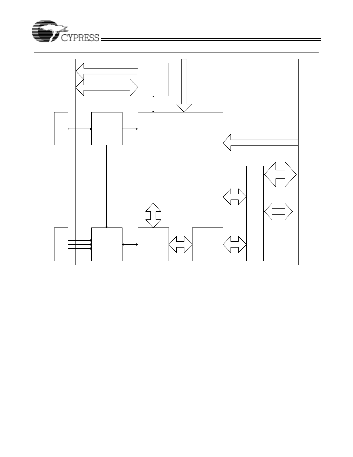
SCL
SDA
I2C-Compatible
Bus Controller
CY7C68300
T
E
S
E
R
24
MHz
XTAL
VBUS
D+
D-
PLL
USB 2.0 XCVR
AT2 Internal Logic
CY Smart USB
FS/HS Engine
Figure 1-1. Block Diagram
4kByte FIFO
A
Control
Data
I
3
t
(
T
A
N
n
E
A
_
T
A
ATA
Interface
Logic
e
e
r
f
a
c
-
s
t
ATA Interf ace
Control Signals
16 Bit ATA Data
a
t
)
e
Document #: 38-08031 Rev. *B Page 5 of 26
A
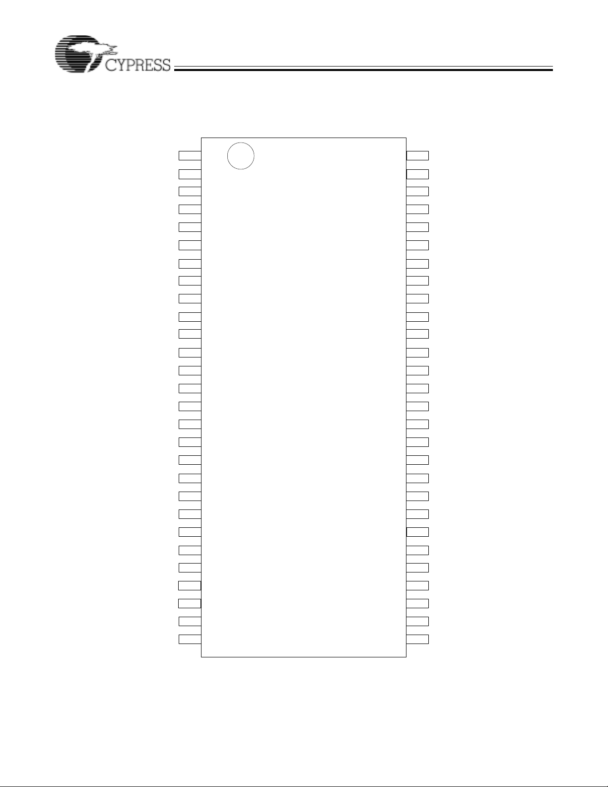
2.0 Pin Assignments
2.1 Pin Diagram
CY7C68300
1
2
3
4
5
6
7
8
9
10
11
12
13
14
15
16
17
DD13
DD14
DD15
GND
NC
Vcc
GND
IORDY
DMARQ
AVcc
XTALOUT
XTALIN
AGND
Vcc
DPLUS
DMINUS
GND
VBUS_PWR_VALID
EZ-USB AT2
CY7C68300A
56-pin SSOP
DD12
DD11
DD10
DD9
DD8
ATA_EN
Vcc
RESET#
GND
ARESET#
CS1#
CS0#
DA2
DA1
DA0
INTRQ
56
55
54
53
52
51
50
49
48
47
46
45
44
43
42
41
40
18
19
20
21
22
23
24
25
26
27
28
Vcc
GND
PU10K
RESERVED
SCL
SDA
Vcc
DD0
DD1
DD2
DD3
DMACK#
DIOR#
DIOW#
Vcc
GND
Vcc
GND
DD7
DD6
DD5
DD4
39
38
37
36
35
34
33
32
31
30
29
Figure 2-1. 56-pin SSOP
Document #: 38-08031 Rev. *B Page 6 of 26
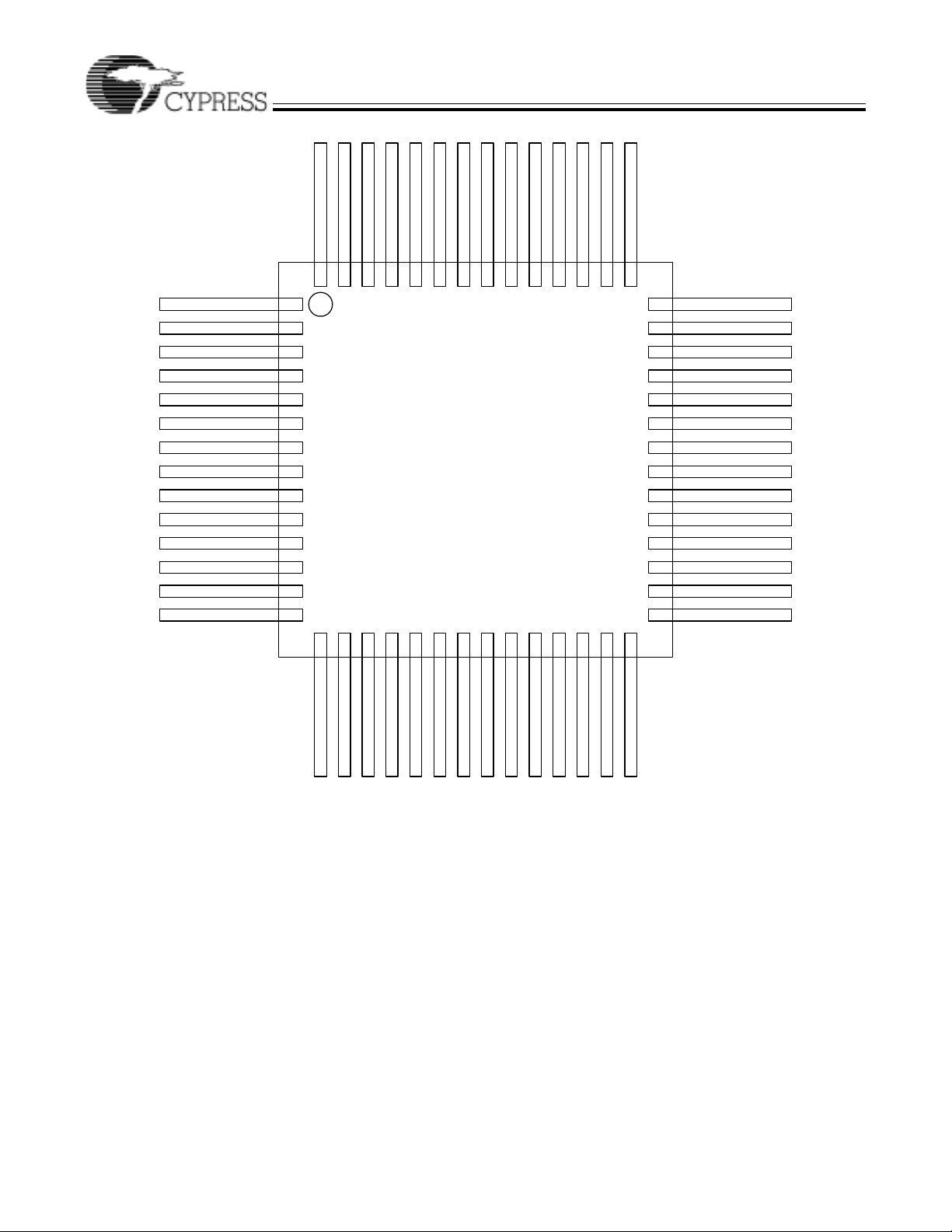
A
CY7C68300
IORDY
DMARQ
AVCC
XTALOUT
XTALIN
AGND
VCC
DPLUS
DMINUS
GND
VCC
GND
PU10K
RESERVED
GND
56
55
1
2
3
4
5
6
7
8
9
10
11
12
13
14
16
15
GND
DD15
DD14
DD13
54
53
52
51
50
EZ-USB AT2
CY7C68300A
56-pin QFN
21
20
19
18
17
DD12
DD11
49
48
23
22
NC
VCC
DD9
DD10
47
24
DD8
46
45
26
25
ATA_EN
44
27
VCC
4328
42
41
40
39
38
37
36
35
34
33
32
31
30
29
RESET#
GND
ARESET#
VBUS_PWR_VALID
CS1#
CS0#
DA2
DA1
DA0
INTRQ
VCC
DMACK#
DIOR#
DIOW#
SCL
SDA
DD0
DD1
DD2
DD3
DD4
DD5
DD6
VCC
DD7
GND
VCC
GND
Figure 2-2. 56-pin QFN
Document #: 38-08031 Rev. *B Page 7 of 26
A
CY7C68300
2.2 Pin Descriptions
SSOP
Note:
QFN
Pin
Pin Pin Name
1 50 DD13 I/O
2 51 DD14 I/O
3 52 DD15 I/O
Pin
T yp e Default Stat e at Start-up Pin Description
[1]
[1]
[1]
Hi-Z ATA Data bit 13.
Hi-Z ATA Data bit 14.
Hi-Z ATA Data bit 15.
4 53 GND GND Ground.
5 54 NC Hi-Z Reserved. This pin should remain a no-connect.
6 55 V
CC
PWR VCC. Connect to 3.3V power source.
7 56 GND GND Ground.
8 1 IORDY I
9 2 DMARQ I
10 3 AV
CC
[1]
[1]
I A TA Control.
I A TA Control.
PWR Analog VCC. Connect the VCC through the shortest path
possible.
11 4 XTALOUT Xtal Xtal 24-MHz Crystal Output (see section 2.3.3).
12 5 XTALIN Xtal Xtal 24-MHz Crystal Input (see section 2.3.3).
13 6 AGND GND Analog Ground. Connect to ground with as short a pa t h as
possible.
14 7 V
CC
15 8 DPLUS I/O Pulled high when Reset is
PWR VCC. Connect to 3.3V power source.
USB D+ Signal (see section 2.3.1).
active. When Reset is
released, the pull-up is
controlled by pin 46(SSOP)/
39(QFN). When VBUS_
PWR_V ALID is high, the line
is pulled up. VBUS_PWR
_VALID is polled at start-up
and then every 20 ms.
16 9 DMINUS I/O Hi-Z USB D- Signal (see section 2.3.1).
17 10 GND GND Ground.
18 11 V
CC
PWR VCC. Connect to 3.3V power source.
19 12 GND GND Ground.
20 13 PU10K Hi-Z Tied to 10k ± 5% pull-up resisto r.
21 14 RESERVED Reserved. Tie to GND.
22 15 SCL O SCL/SDA will be active for
23 16 SDA I/O Data signal for I2C-compatible interface (see section 2.3.2).
24 17 V
CC
several ms at start-up . Then
driven high.
PWR VCC. Connect to 3.3V power source.
Clock signal for I2C-compatible interface (see section 2.3.2).
25 18 DD0 I/O Hi-Z ATA Data bit 0.
26 19 DD1 I/O Hi-Z ATA Data bit 1.
27 20 DD2 I/O Hi-Z ATA Data bit 2.
28 21 DD3 I/O Hi-Z ATA Data bit 3.
29 22 DD4 I/O Hi-Z ATA Data bit 4.
30 23 DD5 I/O Hi-Z ATA Data bit 5.
31 24 DD6 I/O Hi-Z ATA Data bit 6.
32 25 DD7 I/O Hi-Z ATA Data bit 7.
33 26 GND GND Ground.
34 27 V
1. ATA interface pins are not active when ATA_EN is not asserted.
CC
PWR VCC. Connect to 3.3V power source.
Document #: 38-08031 Rev. *B Page 8 of 26

A
CY7C68300
2.2 Pin Descriptions (continued)
SSOP
QFN
Pin
Pin Pin Name
Pin
T yp e Default Stat e at Start-up Pin Description
35 28 GND GND Ground.
36 29 DIOW#
[2]
37 30 DIOR# O/Z
38 31 DMACK# O/Z
39 32 V
CC
40 33 INTRQ I
41 34 DA0 O/Z
42 35 DA1 O/Z
43 36 DA2 O/Z
44 37 CS0# O/Z
45 38 CS1# O/Z
46 39 VBUS_PW
R_VALID
47 40 ARESET# O/Z
[1]
O/Z
Driven high (CMOS) A TA Control.
[1]
Driven high (CMOS) A TA Control.
[1]
Driven high (CMOS) A TA Control.
PWR VCC. Connect to 3.3V power source.
[1]
Input IDE ATA Interrupt request.
[1]
Driven high after 2 ms delay ATA Address.
[1]
Driven high after 2 ms delay ATA Address.
[1]
Driven high after 2 ms delay ATA Address.
[1]
Driven high after 2 ms delay ATA Chip Select.
[1]
Driven high after 2 ms delay ATA Chip Select.
I Input VBUS detection. Indicates to the CY7C68300A that VBUS
power is present.
[1]
ATA Reset.
48 41 GND GND Ground.
49 42 RESET# I Active LOW Reset. R esets the entire chip . This pin is normally
tied to VCC through a 100K resistor, and to GND through a
0.1-µF capacitor, supplying a 10-ms reset.
50 43 V
CC
51 44 ATA_EN I Input – If CY7C68300A is not
PWR VCC. Connect to 3.3V power source.
Active HIGH. ATA interface enable. Allows ATA bus sharing
in mfg mode, polled every 20
ms after start-up. If LOW,
SSOP pins 36–38, 41–45
and 47 or QFN pins 29–31,
with other host devices. S etting ATA_EN=1 enables the ATA
interface for normal operation. Di sabling ATA_EN thre e-states
(High-Z) the ATA interface and halts the ATA interface state
machine logic.
34–38 and 40 are three-
stated.
52 45 DD8 I/O
53 46 DD9 I/O
54 47 DD10 I/O
55 48 DD11 I/O
56 49 DD12 I/O
[1]
Hi-Z ATA Data bit 8.
[1]
Hi-Z ATA Data bit 9.
[1]
Hi-Z ATA Data bit 10.
[1]
Hi-Z ATA Data bit 11.
[1]
Hi-Z ATA Data bit 12.
2.3 Additional Pin Descriptions
2.3.1 DPLUS, DMINUS
DPLUS and DMINUS are the USB sig naling pins, and they sh ould be tie d to the D+ a nd D– pins of the USB conn ector. Because
they operate at high frequencies, the USB signals require special consideration when designing the layout of the PCB.
2.3.2 SCL, SDA
2
The clock and data pins f or the I
C-compatible port s hould be connected to you r configurati on EEPROM an d to VCC through 2.2k
resistors.
2.3.3 XTALIN, XTALOUT
The CY7C68300A requires a 24-MHz signal to derive internal timing. Typically a 24-MHz parallel-resonant fundamental mode
crystal is u sed, but a 24-MHz square w ave from a nother sou rce can also be used. If a cryst al i s used, co nnect the pins to XTALIN
and XTALOUT, and als o through 20-p F capacitors t o GND. If an altern ate clock so urce is used, ap ply it to XTALIN and leave
XT ALO UT ope n.
Note:
2. A # sign after the signal name indicates that it is an active LOW signal.
Document #: 38-08031 Rev. *B Page 9 of 26

A
CY7C68300
24MH z crystal
20pF20pF
Figure 2-3. XTALIN, XTALOUT Diagram
2.3.4 ATA_EN
A TA_EN allows bus sharing with other h ost de vice s. Setti ng ATA_E N = 1 en ables the ATA int erface for norm al op eration . Settin g
A TA_EN = 0 disables (High-Z) the ATA interface pi ns a nd rem ov es the C Y7C 6 830 0A from the USB. Becau se the CY 7C6 830 0A
supports a true low-po wer USB suspend st ate, new functiona lity was added to en sure that transit ions of the A TA_EN signal could
be detected properly under all circumstances. The CY7C68300A will behave in the following manner:
• If A TA_EN transitions to '0' during norm al ope ration, t he CY7C6 8300A wil l disc onnec t from the U SB and drop to a low-po wer
mode.
• If A TA_EN transitions to '1' when in low-power mode and no othe r conditio n is causin g the low- power st ate, the C Y7C68300A
will return to a post-reset state and reconnect to the USB.
• If the CY7C68300A is already in suspend and ATA_EN transitions to '0', the CY7C68300A will resume only long enough to
stop driving the ATA interface (High-Z) and drop back to low-power again.
• If the CY7C68300A is already in suspend and ATA_EN transitions to '1', the CY7C68300A will resume only long enough to
start driving the ATA interface and drop to low-power again.
The A TA_EN pin is sampled at a rate o f 50 times pe r seco nd by the CY7 C68300A inte rnal logic . This pin should b e set to a HIG H
at start-up. Note that disabling the ATA bus with the ATA_EN pin during the middle of a data transfer will result in data loss and
can cause the operating system on the Host computer to crash.
2.3.5 ATA Interface Pins
If a cable is used to connect the CY7C68300A to a UD MA device, the cable must be an 80-pin ca ble as shown in the A T A-6 s pec,
Annex A.
2.3.6 VBUS_PWR_VALID
VBUS_PWR_VALID indicates to the CY7C68300A that power is present on VBUS. This pin is polled by the CY7C68300A at
start-up and t hen every 20ms thereafter . If this pin is ‘1’, the 1.5K pull-up is att a ch ed to D+. If this pin is ‘0’, the CY7 C 68 300A will
release the pullup on D+ as required by the USB specification.
2.3.7 RESET#
Asserting RESET# for 10 ms wil l reset the entire ch ip. This pin is norma lly tied to V
a 0.1-µF capacitor.
R8
100K
NRESET
C1
0.1 uFd
through a 100k resi stor , and to GND throug h
CC
Figure 2-4. Typical Reset Circuit
Document #: 38-08031 Rev. *B Page 10 of 26

A
CY7C68300
3.0 Applications
The CY7C68300A is a high-sp eed USB 2. 0 periphe ral devi ce that connec ts a single ATA or ATAPI storag e devic e to a USB host
using the USB Mass Storage Class protocol.
3.1 Additional Resources
• CY4615 EZ-USB AT2 Reference Design Kit
• USB Specification version 2.0
• ATA Specification T13/1410D Rev 3B
• USB Mass Storage Class Bulk Only Transport Specification, http://www.usb.org/developers/data/devclas s /
usbmassbulk_10.pdf.
4.0 Functional Overview
4.1 USB Signaling Speed
CY7C68300A operates at two of the three rates defined in the USB Specification Revision 2.0 dated April 27, 2000:
• Full speed, with a signaling bit rate of 12 Mbits/sec
• High speed, with a signaling bit rate of 480 Mbits/sec.
CY7C68300 A does not support the low-speed signaling rat e of 1.5 Mbits/sec.
4.2 ATA Interface
The ATA/ATAPI port on the CY7C68300A is compliant with the Information Technology AT Attachment with Packet Interface 6
(ATA/ATAPI-6) Specification, T13/1410D Rev 3B. The CY7C68300A supports ATAPI packet commands over USB. Additionally,
the CY7C68300A t ranslates A TAPI SFF-8070i comman ds to A T A c ommands for se amless inte gration of A TA devices with gen eric
Mass Storage Class Bulk Only Transport drivers.
5.0 Enumeration
During the power-up sequence, internal logic checks the I2C-compatible port for an EEPROM whose first two bytes are both
0x4D. If a valid signature is found, the CY7C68300A uses the values stored in the EEPROM to configure the USB descriptors
for normal operation. If an invalid EEPROM signa ture is read, or if no EEPROM is detected, the CY7C68300 A defaults into Board
Manufacturing Test Mode. The two modes of operation are described in subsections 5.1 and 5.2, below.
5.1 Board Manufacturing Test Mode
In Board Manufacturing Test Mode, the chip behaves as a USB 2.0 device but the ATA/ATAPI interface is not active. The
CY7C68300A allows for reading and writing an EEPROM and for board level testing through vendor specific ATAPI commands
utilizing the CBW Command Block as described in the USB Mass Storage Class Bulk-Only Transport Specification. There is a
vendor-specific ATAPI command for the EEPROM access (CfgCB) and one for the board level testing (MfgCB).
5.1.1 CfgCB
The cfg_load and cfg_ read vendor-spec ific commands are p assed down through the bulk pipe in the CB WCB portion of the CBW .
The format of this CfgCB is shown be low. Byte 0 will be a vendor-specific command designa tor whos e value is config urable and
set in the configuration d ata (EEPROM ad dress 0x04). Byte 1 must be set to 0x26 to identify CfgCB. By te 2 is reserv ed and must
be set to zero. Byte 3 i s used to de termine the m emory sourc e to write/rea d. For the CY7C6830 0A, this by te must be set to 0 x02,
meaning the EEPROM. Bytes 4 and 5 will be used to determine the start address. For the CY7C68300A, this must always be
0x0000. Bytes 6 through 15 are reserved and should be set to zero.
The data transferred to the EEPROM must be in the fo rmat specifie d in Table 5-6 of this data sheet. Maximum data transfer size
is 255 bytes.
The data transfer length is determined by the CBW Data Transfer Length specified in bytes 8 through 11 (dCBWDataTransferLength) of the CBW . The type/dire ction of the command will be de termined by the direct ion bit specified in byte 12 , bit 7 (bmCBWFlags) of the CBW.
Document #: 38-08031 Rev. *B P age 11 of 26

A
CY7C68300
Table 5-1. Command Block Wrapper
7 6 54321 0
0–3 DCBWSignature
4–7 dCBWTag
8–11 (08h-0Bh) dCBWDataTransferLength
12 (0Ch) bwCBWFLAGS
Dir Obsolete Reserved (0)
13 (0Dh) Reserved (0) bCBWLUN
14 (0Eh) Reserved (0) bCBWCBLength
15–30 (0Fh1Eh) CBWCB (CfgCB or MfgCB)
Table 5-2. Example CfgCB
CfgCB Byte Descriptions Bits
76543210
0 bVSCBSignature (set in configuration bytes) 00100100
1 bVSCBSubCommand (must be 0x26) 00100110
2 Reserved (must be set to zero) 00000000
3 Data Source (must be set to 0x02) 00000010
4 Start Address (LSB) (must be set to zero) 00000000
5 Start Address (MSB) (must be set to zero) 00000000
6–15 Reserved (must be set to zero) 00000000
5.1.2 MfgCB
The mfg_load and mfg_rea d vendo r-spec ific comm ands will be pas sed down thro ugh the bul k pipe in the CBWCB portion of the
CBW. The format of this MFGCB is shown below. Byte 0 is a vendor-specific command designator whose value is configurable
and set in the configuration data. Byte 1 must be 0x27 to identify MfgCB. Byte 2–15 are reserved and must be set to zero.
The data transfer len gth will be de termin ed by the CBW D ata T rans fer Lengt h speci fied in by tes 8 thro ugh 11 (dCBWDataTrans ferLength) of the CBW. The type/direction of the command is determined by th e directi on bit spe cifie d in byte 12 , bit 7 (bmCBWFlags) of the CBW.
Table 5-3. Example MfgCB
MfgCB Byte Description Bits
0 bVSCBSignature (set in configuration bytes) 00100100
1 bVSCBSubCommand (hardcoded 0x27) 00100111
2–15 Reserved (must be zero) 00000000
5.1.2.1 Mfg_load
During a mfg_load, the CY7C68300A goes into Manufacturing Test Mode. Manufacturing Test Mode is provided as a means to
implement board o r system lev el interconnect tests. Dur ing Manufacturi ng Test Mode operation, all outputs n ot directly associated
with USB operation are controllable. Normal control of the output pins are disabled. Control of the select CY7C68300A IO pins
and their three-state controls are mapped to the ATAPI data packet associated with this request. (See the following table for
explanation of the req uired m fg_loa d dat a for mat.) Thi s requir es a write o f seven bytes. To exit Manufactur ing Test Mode, a hard
reset (#RESET) is required.
Table 5-4. Mfg_load Data Format
Byte Bit(s) Test/Three-state Control Function
00Reserved
0 3:1 DA[2:0]
0 5:4 CS#[1:0]
06Reserved
0 7 ARESET#
1 0 NDIOW
Document #: 38-08031 Rev. *B Page 12 of 26

A
CY7C68300
Table 5-4. Mfg_load Data Format (continued)
Byte Bit(s) Test/Three-state Control Function
1 1 NDIOR
1 2 NDMACK
13:6Reserved
1 7 DD[15:0] Three-state (0 = three-state DD pins, 1 = enable DD pins).
2 7:0 DD[7:0]
3 7:0 DD[15:8]
47:0Reserved
57:0Reserved
67:0Reserved
5.1.2.2 Mfg_read
This USB request returns a “sn aps hot in ti me” of s elect CY 7C683 00A inpu t pins. The inpu t pin states are bit-wise mapped to the
A TAPI data associated with thi s req ues t. C Y7C68 300A input pins not directly associated with USB operation can be sa mpled at
any time during Manufa cturing Test Mode operation. See the fol lowi ng t able for a n expla nation of the mf g_read d ata format. Th e
data length shall always be eight bytes.
Table 5-5. Mfg_read Data Format
Byte Bit(s) Test/Three-state Control Function
00INTRQ
0 5:1 Reserved. This data should be ignored.
0 6 VBUS_PWR_VALID
0 7 ARESET# (output value only)
1 2:0 Reserved. This data should be ignored.
1 3 IORDY
14DMARQ
1 5 ATA_EN
1 6 Reserved. This data should be ignored.
1 7 DD[15:0] Three-state
2 7:0 DD[7:0]
3 7:0 DD[15:8]
4 7:0 Reserved. This data should be ignored.
5 7:0 Reserved. This data should be ignored.
6 7:0 Reserved. This data should be ignored.
7 7:0 Reserved. This data should be ignored.
5.2 Normal Operation Mode
In Normal Operation Mode, the chip behaves as a USB 2.0 to ATA/ATAPI bridge. This includes all typical USB device states
(powered, configured, etc.). The USB descriptors are returned according to the values stored in the external EEPROM. An
external EEPROM is required for Mass Storage Class Bulk-Only Transpor t complia nce, s ince a unique serial number is req uired
for each device. Also, Cypress requires customers to use their own Vendor and Product IDs for final products.
5.3 EEPROM Organization
The contents of the 256-byte (2048-bit) two-wire serial EEPROM are arranged as follows. The column labeled “Required
Contents” contains the values that must be used for proper operation of the CY7C68300A. The column labeled “Suggested
Contents” contains suggested values for the bytes that are defined by the manufacturer. Some values, such as the Vendor ID
and device and device serial number, must be customized to meet USB compliance. See section 5.1 for details on how to use
vendor-specific ATAPI com mands t o read and p rogram the EEP ROM. The seria l EEPROM mus t be hard-wired to addre ss 0 x04.
This means that A0 and A1 of the serial EEPROM must be tied to ground and that A2 must be tied to 3.3V.
Document #: 38-08031 Rev. *B Page 13 of 26

A
CY7C68300
Table 5-6. EEPROM Organization
EEPROM
Address Field Name Field Description
Configuration
0x00 I2C-compatible memory
device signature (LSB )
0x01 I
0x02 APM Value ATA Device Automatic Power Management Value. If an
0x03 ATA Initialization Timeout Time in 128-ms granularity before the CY7C68300A stops
0x04 AT A Command Designator V alue in the first byte of the CBW CB fi eld that designates that
0x05 Reserved Bits(7:4) Set to 0 0x07
Notes:
3. At least one reset must be enabled. Do not set SRST to 0 and Skip Pin Reset to 1at the same time.
4. SRST Enable must be set in conjunction with Skip Pin Reset. Setting this bit causes the CY7C68300A to bypass ARESET # during initialization. All reset events
except a power-on reset utilize SRST as the drive mechanism.
2
C-compatible memory
device signature (MSB)
BUSY Bit Delay Bit (3)
Short Packet Before Stall Bit (2)
SRST Enable Bit (1)
Skip Pin Reset Bit (0)
LSB I2C-compatible memory device signature byte. 0x4D
MSB I2C-compatible memory device signature byte. 0x4D
attached ATA device supports APM and this field contains
other than 0x00, the CY7C68300A will issue a
SET_FEATURES command to Enable APM with this value
during the drive initialization proc ess. Setting APM Value to
0x00 disables this functionality. This value is ignored with
ATAPI devices.
polling the AL T STAT regi ster for reset co mplete and res tarts
the reset process (0x80 = 16.4 seconds).
the CB is t o be decoded as v endor s pecific AT A command s
instead of the ATAPI command block. See section 4.0 for
more detail on how this byte is used.
Enables a delay of up to 120 m s at each rea d of the DRQ bit
where the device data length does not match the host data
length. This allows the CY7C68300A to work with most
devices that incorrectly clear the BUSY bit before a valid
status is present.
Determines if a short packet is sent prior to the STALL of an
IN endpoint. The USB Mass Storage Class Bulk-Only Speci-
fication allows a device to send a short or zero-length IN
packet prior to returning a STALL handshake for certain
cases. Certain host controller drivers may require a short
packet prio r to STALL.
1 = Force a short packet before STALL.
0 = Don’t force a short packet before STALL.
Determines if the CY7C 68300A is to do a SRST reset du ring
drive initialization.
1 = Perform SRST during initialization.
0 = Don’t perform SRST during initialization.
Skip ATA_NRESET assertion.
0 = Allow ARESET# assertion for all resets.
1 = Disable ARESET# assertion except for power-on reset
cycles.
[3]
[4]
Required
Contents
Suggested
Contents
0x00
0x80
0x24
Document #: 38-08031 Rev. *B Page 14 of 26

A
CY7C68300
Table 5-6. EEPROM Organization (continued)
EEPROM
Address Field Name Field Description
0x06 ATA UDMA Enable Bit (7)
ATAPI UDMA Enable Bit (6)
UDMA Modes Bit (5:0)
0x07 Reserved
PIO Modes
0x08 Reserved Must be set to 0x00. 0x00
0x09 Reserved Must be set to 0x00. 0x00
0x0A Reserved Must be set to 0x00. 0x00
0x0B Reserved Must be set to 0x00. 0x00
0x0C Reserved Must be set to 0x00. 0x00
0x0D Reserved Must be set to 0x00. 0x00
0x0E Reserved Must be set to 0x00. 0x00
0x0F Reserved Must be set to 0x00. 0x00
Device Descriptor
0x10 bLength Length of device descriptor in bytes. 0x12
0x11 bDescriptor Type Descriptor type. 0x01
0x12 bcdUSB (LSB) USB Specification release number in BCD. 0x00
0x13 bcdUSB (MSB) 0x02
0x14 bDeviceClass Device class. 0x00
0x15 bDeviceSubClass Device subclass. 0x00
Enable Ultra DMA data transfer supp ort for A TAPI devices. If
enabled, and if the ATAPI device reports UDMA support for
the indicated modes, the CY7 C68300A will utilize UDMA data
transfers at the highest negotiated rate possible.
0 = Disable ATA device UDMA support.
1 = Enable ATA device UDMA support.
Enable Ultra DMA data transfer supp ort for A TAPI devices. If
enabled, and if the ATAPI device reports UDMA support for
the indicated modes, the CY7 C68300A will utilize UDMA data
transfers at the highest negotiated rate possible.
0 = Disable ATAPI device UDMA support.
1 = Enable ATAPI device UDMA support.
These bits select which UDMA modes, if supported, are
enabled. Setting to 1 enables. Multiple bits may be set. The
CY7C68300A will operate in the highest enabled UDMA
mode supported by the device. The CY7C68 300 A supp orts
UDMA modes 2 and 4 only.
Bit Descriptions
5 Reserved. Must be set to 0.
4 Enable UDMA mode 4.
3 Reserved. Must be set to 0.
2 Enable UDMA mode 2.
1 Reserved. Must be set to 0.
0 Reserved. Must be set to 0.
Bits(7:2)
Bits(1:0)
These bits select which PIO modes, if supported, are
enabled. Setting to 1 enables. Multiple bits may be set. The
CY7C68300A will operate i n th e highest enabled PIO mod e
supported by the device. The CY7C68300A supports PIO
modes 0, 3, and 4 only. PIO mode 0 is always enabled by
internal logic.
Bit Descriptions
1 Enable PIO mode 4.
0 Enable PIO mode 3.
Required
Contents
Suggested
Contents
0xD4
0x03
Document #: 38-08031 Rev. *B Page 15 of 26

A
CY7C68300
Table 5-6. EEPROM Organization (continued)
EEPROM
Address Field Name Field Description
0x16 bDeviceProtocol Device protocol. 0x00
0x17 bMaxPacketSize0 USB packet size supported for default pipe. 0x40
0x18 idVendor (LSB) Vendor ID . Cypress’ s Vendor ID may only be used for evalu0x19 idVendor (MSB) 0x04
0x1A idProduct (LSB) Product ID. 0x30
0x1B idProduct (MSB) 0x68
0x1C bcdDevice (LSB) Device release number in BCD LSB (product release
0x1D bcdDevice (MSB) Device releas e num ber in BCD MSB (sil ic on rele as e
0x1E iMan ufacturer Index to manufacturer string. T his entry must equal ha lf of the
0x1F iProduct Index to product string. This entry must equal half of the
0x20 iSerialNumber Index to serial number string. This entry must equal half of
0x21 bNumConfigurations Number of configurations supported. 0x01
Device Qualifier
0x22 bLength Length of device descriptor in bytes. 0x0A
0x23 bDescriptor Type Descriptor type. 0x06
0x24 bcdUSB (LSB) USB Specification release number in BCD. 0x00
0x25 bcdUSB (MSB) USB Specification release number in BCD. 0x02
0x26 bDeviceClass Device class. 0x00
0x27 bDeviceSubClass Device subclass. 0x00
0x28 bDeviceProtocol Device protocol. 0x00
0x29 bMaxPacketSize0 USB packet size supported for default pipe. 0x40
0x2A bNumConfigurations Number of configurations supported. 0x01
0x2B bReserved Reserved for future use. Must be set to zero. 0x00
High-speed Configuration Descriptor
0x2C bLength Length of configuration descriptor in bytes. 0x09
0x2D bDescriptorType Descript or type. 0x02
0x2E bTotalLength (LSB) Number of bytes returned in this confi guration. Th is includes
0x2F bTotalLength (MSB) 0x00
0x30 bNumInterfaces Number of interfaces supported. 0x01
0x31 bConfiguration Value The value to use as an argument to Set Configuration to
0x32 iConfiguration Index to the configuration string. This entry must equal half
ation purposes, and not in released products.
number).
number).
address value where the strin g starts or 0x00 if the string does
not exist.
address value where the strin g starts or 0x00 if the string does
not exist.
the address value where the strin g start s or 0x00 if the string
does not exist. The USB Mass Storage C lass Bulk -O nly
Transport Specification requires a unique serial number (in
upper case, hexidecimal characters) for each device.
the configuration descriptor plus all the interface and
endpoint descriptors.
select the configuration. This value must be set to 0x01.
of the address value where the string starts or 0x00 if the
string does not exist.
Required
Contents
0x20
0x01
Suggested
Contents
0xB4
0x01
0x00
0x38
0x4E
0x64
0x00
Document #: 38-08031 Rev. *B Page 16 of 26

A
CY7C68300
Table 5-6. EEPROM Organization (continued)
EEPROM
Address Field Name Field Description
0x33 bmAttributes Device attributes for this configuration.
0x34 bMaxPower Maximum power consumption for this configuration. Units
High-speed Interface and Endpoint Descriptors
Interface Descriptor
0x35 bLength Length of interface descriptor in bytes . 0x09
0x36 bDescriptorType Descriptor type. 0x04
0x37 bInterfaceNumber Interface number. 0x00
0x38 bAlternateSetting Alternate setting. 0x00
0x39 bNumEndpoints Num ber of endpoints. 0x02
0x3A bInterfaceClass Interface class. 0x08
0x3B bInterfaceSubClass Interface subclass. 0x06
0x3C bInterfaceProtocol Interface protocol. 0x50
0x3D iInterface Index to first interface string. Thi s entry must equal half of the
USB Bulk In Endpoint
0x3E bLength Length of this descriptor in bytes. 0x07
0x3F bDescriptorType Endpoint descriptor type. 0x05
0x40 bEndpointAddress This is an In endpoint, endpoint number 8. 0x88
0x41 bmAttributes This is a bulk endpoint. 0x02
0x42 wMaxPacketSize (LSB) Max data transfer size. 0x00
0x43 wMaxPacketSize (MSB) 0x02
0x44 bInterval HS interval for polling (max. NAK rate). 0x00
USB Bulk Out Endpoint
0x45 bLength Length of this descriptor in bytes. 0x07
0x46 bDescriptorType Endpoint d escriptor type. 0x05
0x47 bEndpointAddress This is an Out endpoint, endpoint number 2. 0x02
0x48 bmAttributes This is a bulk endpoint. 0x02
0x49 wMaxPacketSize (LSB) Max data transfer size. 0x00
0x4A wMaxPacketSize (MSB) 0x02
0x4B bInterval HS interval for polling (max. NAK rate). 0x00
Full-speed Configuration Descriptor
0x4C bLength Length of configuration descriptor in bytes. 0x09
0x4D bDescriptorType Descript or type. 0x02
0x4E bTotalLength (LSB) Number of bytes returned in this confi guration. Th is includes
0x4F bTotalLength (MSB) 0x00
0x50 bNumInterfaces Number of interfaces supported. 0x01
0x51 bConfiguration Value The value to use as an argument to Set Configuration to
Bit Descriptions
7 Reserved. Must be set to 1.
6 Self-powered. Must be set to 1.
5 Remote wake-up. Must be set to 0.
4–0 Reserved. Must be set to 0.
used are mA*2 (i.e., 0x31 = 98 mA, 0xF9 = 498 mA). 0x00
reported for self-powered devices.
address value where the strin g starts or 0x00 if the string does
not exist.
the configuration descriptor plus all the interface and
endpoint descriptors.
select the configuration.
Required
Contents
0xC0
0x20
0x01
Suggested
Contents
0x00
0x00
Document #: 38-08031 Rev. *B Page 17 of 26

A
CY7C68300
Table 5-6. EEPROM Organization (continued)
EEPROM
Address Field Name Field Description
0x52 iConfiguration Index to configuration string. This entry must equal h alf of the
address value where the strin g starts or 0x00 if the string does
not exist.
0x53 bmAttributes Device attributes for this configuration.
Bit Descriptions
7 Reserved. Must be set to 1.
6 Self-powered. Must be set to 1.
5 Remote wake-up. Must be set to 0.
4–0 Reserved. Must be set to 0.
0x54 bMaxPower Maximum power consumption for the second configuration.
Units used are mA*2 (i.e., 0x31 = 98 mA, 0xF9 = 498 mA).
Full-speed Interface and Endpoint Descriptors
Interface Descriptor
0x55 bLength Length of interface descriptor in bytes . 0x09
0x56 bDescriptorType Descriptor type. 0x04
0x57 bInterfaceNumber Interface number. 0x00
0x58 bAlternateSettings Alternate settings. 0x00
0x59 bNumEndpoints Num ber of endpoints. 0x02
0x5A bInterfaceClass Interface class. 0x08
0x5B bInterfaceSubClass Interface subclass. 0x06
0x5C bInterfaceProtocol Interface protocol. 0x50
0x5D iInterface Index to first interface string. Thi s entry must equal half of the
address value where the strin g starts or 0x00 if the string does
not exist.
USB Bulk InEndpoint
0x5E bLength Length of this descriptor in bytes. 0x07
0x5F bDescriptorType Endpoint descriptor type. 0x05
0x60 bEndpointAddress This is an In endpoint, endpoint number 8. 0x88
0x61 bmAttributes This is a bulk endpoint. 0x02
0x62 wMaxPacketSize (LSB) Max data transfer size. 0x40
0x63 wMaxPacketSize (MSB) 0x00
0x64 bInterval Does not apply to FS bulk endpoints. Must be set to 0. 0x00
USB Bulk Out Endpoint
0x65 bLength Length of this descriptor in bytes. 0x07
0x66 bDescriptorType Endpoint d escriptor type. 0x05
0x67 bEndpointAddress This is an Out endpoint, endpoint number 2. 0x02
0x68 bmAttributes This is a bulk endpoint. 0x02
0x69 wMaxPacketSize (LSB) Max data transfer size. 0x40
0x6A wMaxPacketSize (MSB) 0x00
0x6B bInterval Does not apply to FS bulk endpoints. Must be set to 0. 0x00
String Descriptor Examples (Note: The values in these strings are given as examples only and should not be used in final
products. Designers are encouraged to modify the string values to reflect the final product, since they are what users will see
with their operating systems.)
USB String Descriptor–Index 0 (LANGID)
0x6C bLength LANGID string descriptor length in bytes. 0x04
0x6D bDescriptorType Descript or type. 0x03
Required
Contents
0xC0
0x00
Suggested
Contents
0x00
0x00
Document #: 38-08031 Rev. *B Page 18 of 26

A
CY7C68300
Table 5-6. EEPROM Organization (continued)
EEPROM
Address Field Name Field Description
0x6E LANGID (LSB) Language supported.
0x6F LANGID (MSB) 0x04
USB String Descriptor–Man ufac turer
0x70 bLength String descriptor length in bytes (including bLength). 0x2C
0x71 bDescriptorType Descriptor type. 0x03
0x72 bString Unicode character. “C” 0x43
0x73 bString (“NUL”) 0x00
0x74 bString Unicode character. “y” 0x79
0x75 bString (“NUL”) 0x00
0x76 bString Unicode character. “p” 0x70
0x77 bString (“NUL”) 0x00
0x78 bString Unicode character. “r” 0x72
0x79 bString (“NUL”) 0x00
0x7A bString Unicode character. “e” 0x65
0x7B bString (“NUL”) 0x00
0x7C bString Unicode character. “s” 0x73
0x7D bString (“NUL”) 0x00
0x7E bString Unicode character. “s” 0x73
0x7F bString (“NUL”) 0x00
0x80 bString Unicode character. “ ” 0x20
0x81 bString (“NUL”) 0x00
0x82 bString Unicode character. “S” 0x53
0x83 bString (“NUL”) 0x00
0x84 bString Unicode character. “e” 0x65
0x85 bString (“NUL”) 0x00
0x86 bString Unicode character. “m” 0x6D
0x87 bString (“NUL”) 0x00
0x88 bString Unicode character. “i” 0x69
0x89 bString (“NUL”) 0x00
0x8A bString Unicode character. “c” 0x63
0x8B bString (“NUL”) 0x00
0x8C bString Unicode character. “o” 0x6F
0x8D bString (“NUL”) 0x00
0x8E bString Unicode character. “n” 0x6E
0x8F bString (“NUL”) 0x00
0x90 bString Unicode character. “d” 0x64
0x91 bString (“NUL”) 0x00
0x92 bString Unicode character. “u” 0x75
0x93 bString (“NUL”) 0x00
0x94 bString Unicode character. “c” 0x63
0x95 bString (“NUL”) 0x00
0x96 bString Unicode character. “t” 0x74
0x97 bString (“NUL”) 0x00
Note:
5. See http://www.usb.org for LANGID documentation (the code for English is 0x0409).
[5]
Required
Contents
Suggested
Contents
0x09
Document #: 38-08031 Rev. *B Page 19 of 26

A
CY7C68300
Table 5-6. EEPROM Organization (continued)
EEPROM
Address Field Name Field Description
0x98 bString Unicode character. “o” 0x6F
0x99 bString (“NUL”) 0x00
0x9A bString Unicode character. “r” 0x72
0x9B bString (“NUL”) 0x00
USB String Descriptor–Product
0x9C bLength String descriptor length in bytes (including bLength). 0x2C
0x9D bDescriptorType Descript or type. 0x03
0x9E bString Unicode character. “U” 0x55
0x9F bString (“NUL”) 0x00
0xA0 bString Unicode character. “S” 0x53
0xA1 bString (“NUL”) 0x00
0xA2 bString Unicode character. “B” 0x42
0xA3 bString (“NUL”) 0x00
0xA4 bString Unicode character. “2” 0x32
0xA5 bString (“NUL”) 0x00
0xA6 bString Unicode character. “.” 0x2E
0xA7 bString (“NUL”) 0x00
0xA8 bString Unicode character. “0” 0x30
0xA9 bString (“NUL”) 0x00
0xAA bString Unicode character. “ ” 0x20
0xAB bString (“NUL”) 0x00
0xAC bString Unicode character. “S” 0x53
0xAD bString (“NUL”) 0x00
0xAE bString Unicode character. “t” 0x74
0xAF bString (“NUL”) 0x00
0xB0 bString Unicode character. “o” 0x6F
0xB1 bString (“NUL”) 0x00
0xB2 bString Unicode character. “r” 0x72
0xB3 bString (“NUL”) 0x00
0xB4 bString Unicode character. “a” 0x61
0xB5 bString (“NUL”) 0x00
0xB6 bString Unicode character. “g” 0x67
0xB7 bString (“NUL”) 0x00
0xB8 bString Unicode character. “e” 0x65
0xB9 bString (“NUL”) 0x00
0xBA bString Unicode character. “ ” 0x20
0xBB bString (“NUL”) 0x00
0xBC bString Unicode character. “D” 0x44
0xBD bString (“NUL”) 0x00
0xBE bString Unicode character. “e” 0x65
0xBF bString (“NUL”) 0x00
0xC0 bString Unicode character. “v” 0x76
0xC1 bString (“NUL”) 0x00
0xC2 bString Unicode character. “i” 0x69
Required
Contents
Suggested
Contents
Document #: 38-08031 Rev. *B Page 20 of 26

A
CY7C68300
Table 5-6. EEPROM Organization (continued)
EEPROM
Address Field Name Field Description
0xC3 bString (“NUL”) 0x00
0xC4 bString Unicode character. “c” 0x63
0xC5 bString (“NUL”) 0x00
0xC6 bString Unicode character. “e” 0x65
0xC7 bString (“NUL”) 0x00
USB String Descriptor–Se ri al Num ber (Note: The USB Mass Storage Class requires a unique serial num be r in eac h d ev ice .
Not providing a unique serial nu mb er will crash the operati ng syst em. The ser ial number mu st be at leas t a minimu m size of 12
characters. Some hosts will only treat the last 12 characters of the serial number as unique.)
0xC8 bLength String descriptor length in bytes (including bLength). 0x22
0xC9 bDescriptor Type Descriptor type. 0x03
0xCA bString Unicode character. “1” 0x31
0xCB bString (“NUL”) 0x00
0xCC bString Unicode character. “2” 0x32
0xCD bString (“NUL”) 0x00
0xCE bString Unicode character. “3” 0x33
0xCF bString (“NUL”) 0x00
0xD0 bString Unicode character. “4” 0x34
0xD1 bString (“NUL”) 0x00
0xD2 bString Unicode character. “5” 0x35
0xD3 bString (“NUL”) 0x00
0xD4 bString Unicode character. “6” 0x36
0xD5 bString (“NUL”) 0x00
0xD6 bString Unicode character. “7” 0x37
0xD7 bString (“NUL”) 0x00
0xD8 bString Unicode character. “8” 0x38
0xD9 bString (“NUL”) 0x00
0xDA bString Unicode character. “9” 0x39
0xDB bString (“NUL”) 0x00
0xDC bString Unicode character. “0” 0x30
0xDD bString (“NUL”) 0x00
0xDE bString Unicode character. “A” 0x41
0xDF bString (“NUL”) 0x00
0xE0 bString Unicode character. “B” 0x42
0xE1 bString (“NUL”) 0x00
0xE2 bString Unicode character. “C” 0x43
0xE3 bString (“NUL”) 0x00
0xE4 bString Unicode character. “D” 0x44
0xE5 bString (“NUL”) 0x00
0xE6 bString Unicode character. “E” 0x45
0xE7 bString (“NUL”) 0x00
0xE8 bString Unicode character. “F” 0x46
0xE9 bString (“NUL”) 0x00
0xEA to
0xFF
Unused ROM Space Amount of unused RO M space will vary de pending on strings. 0xFF
Required
Contents
Suggested
Contents
Document #: 38-08031 Rev. *B Page 21 of 26

A
CY7C68300
6.0 Absolute Maximum Ratings
Storage Temperature ............................................................................................................................................–65°C to +150°C
Ambient Temperature with power supplied.................................................................................................................0°C to +70°C
Supply Voltage to Ground Potential.........................................................................................................................–0.5V to +4.0V
DC Input Voltage to Any Input Pin......................................................................................................................................... 5.25V
DC Voltage Applied to Outputs in High-Z State ............................................................................................. –0.5V to V
Power Dissipation.............................................................................................................................................................. 936 mW
Static Discharge Voltage....................................................................................................................................................> 2000V
Max Output Current per IO port............................................................................................................................................ 10 mA
CC
+ 0.5V
7.0 Operating Conditions
[6]
TA (Ambient Temperature Under Bias).......................................................................................................................0°C to +70°C
Supply Voltage.........................................................................................................................................................+3.0V to +3.6V
Ground V oltage....................................... ...... ..... ...... ..... .............................................................................................................. 0V
(Oscillator or Crystal Frequency) .............................................................................................................. 24 MHz ± 100 ppm
F
osc
......................................................................................................................................... ...................................Parallel Resonant
8.0 DC Characteristics
Parameter Description Conditions Min. Typ. Max. Unit
V
CC
V
IH
V
IL
I
I
V
OH
V
OL
I
OH
I
OL
C
IN
I
CC
I
CC
I
SUSP
T
RESET
Supply Voltage 3.0 3.3 3.6 V
Input High Voltage 2 5.25 V
Input Low Voltage –0.5 0.8 V
Input Leakage Current 0 < VIN < V
Output Voltage High I
Output Voltage Low I
= 4 mA 2.4 V
OUT
= –4 mA 0.4 V
OUT
CC
+ 10 µA
Output Current High 4mA
Output Current Low 4mA
Input Pin Capacitance All but D+/D- 10 pF
Only D+/D- 15 pF
Supply Current USB High Speed 235 260 mA
Supply Current USB Full Speed 90 150 mA
Suspend Current Connected 250 400 µA
Disconnected 30 180 µA
Reset Time After Valid Power VCC min = 3.0V 1.91 ms
9.0 AC Electrical Characteristics
9.1 USB Transceiver
Complies with the USB 2.0 specification.
9.2 ATA Timing
The ATA interface supports ATA PIO modes 0, 3, and 4, and Ultra DMA modes 2 and 4 per the ATA Specification T13/1410D
Rev. 3B.
Note:
6. If an alternate clock source is input on XTALIN it must be supplied with standard 3.3V signaling characteristics and XTALOUT must be left floating.
Document #: 38-08031 Rev. *B Page 22 of 26

A
10.0 Ordering Information
Part Number Package Type
CY7C68300A-PVC 56 SSOP
CY7C68300A-LFC 56 QFN
CY4615A EZ-USB AT2 Reference Design Kit
11. 0 Package Diagrams
.020
28
1
0.395
0.420
0.292
0.299
DIMENSIONS IN INCHES MIN.
CY7C68300
MAX.
0.088
0.092
0.80[0.031]
29
0.720
0.730
0.025
BSC
0.008
0.0135
56
0.008
0.016
0.095
0.110
SEATING PLANE
0.110
GAUGE PLANE
.010
0.024
0°-8°
0.040
0.005
0.010
51-85062-*C
Figure 11-1. 56-lead Shrunk Small Outline Package 056
56-Lead QFN 8 x 8 MM LF56A
TOP VIEW
A
1
2
DIA.
7.90[0.311]
8.10[0.319]
7.70[0.303]
7.80[0.307]
N
7.80[0.307]
7.70[0.303]
1.00[0.039] MAX.
0.80[0.031] MAX.
8.10[0.319]
7.90[0.311]
SIDE VIEW
0.08[0.003]
0.05[0.002] MAX.
0.20[0.008] REF.
0.30[0.012]
0.50[0.020]
C
BOTTOM VIEW
E-PAD
(PAD SIZE VARY
BY DEVICE TYPE)
0.18[0.007]
0.28[0.011]
PIN1 ID
N
0.20[0.008] R.
1
2
0.45[0.018]
6.55[0.258]
6.45[0.254]
0.24[0.009]
0°-12°
0.50[0.020]
C
SEATING
PLANE
6.45[0.254]
6.55[0.258]
0.60[0.024]
(4X)
51-85144-*D
Figure 11-2. 56-lead Quad Flatpack No Lead (8 x 8 mm) LF56A
Document #: 38-08031 Rev. *B Page 23 of 26

A
CY7C68300
12.0 PCB Layout Recommendations
The following recommendations should be followed to ensure reliable high-performance operation.
• At least a four-layer impedance controlled boards are required to maintain signal quality.
• Specify impedance targets (ask your board vendor what they can achieve).
• To control impedance, maintain trace widths and trace spacing.
• Minimize stubs to minimize reflected signals.
• Connections between the USB connector shell and signal ground must be done near the USB connector.
• Bypass/flyback caps on VBus, near connector, are recommended.
• DPLUS and DMINUS trace lengths should be kept to within 2 mm of each other in length, with preferred length of 20-30mm.
• Maintain a solid ground plane under the DPLUS and DMINUS traces. Do not allow the plane to be split under these traces.
• It is preferred is to have no vias placed on the DPLUS or DMINUS trace routing.
• Isolate the DPLUS and DMINUS traces from all other signal traces by no less than 10 mm.
Source for recommendations:
• EZ-USB FX2 PCB Design Recommendations, http:///www.cypress.com/cfuploads/support/app_notes/FX2_PCB.pdf.
• High-speed USB Platform Design Guidelines, http://www.usb.org/developers/data/hs_usb_pdg_r1_0.pdf.
13.0 Quad Flat Package No Leads (QFN) Package Design Notes
Electrical contact of the part to the Printed Circuit Board (PCB) is made by soldering the leads on the bottom surface of the
package to the PCB. Henc e, s pec ia l atte nti on is requ ire d to the heat t rans fer a rea be low th e p ac ka ge to prov id e a goo d the rmal
bond to the circuit bo ard. A Copper (Cu) fil l is to be designed into the PCB as a the rmal pad under th e package. He at is transferred
from the CY7C68300A throug h the device ’s met al p add le on the bot tom side of the p ack age. Heat from here is c onduc ted to the
PCB at the thermal pad. It is then conducted from the thermal pad to the PCB inner ground plane by a 5 x 5 array of Via. A Via
is a plated throu gh-hole in th e PCB with a finish ed dia meter of 1 3 mil. The Q FN’ s met al die p addle must be soldered to the PC B’s
thermal pad. Solder mask is placed on the board top side over each Via to resist solder flow into the Via. The mask on the top
side also minimizes outgassing during the solder reflow process.
For further information on this package design please refer to the application note “Surface Mount Assembly of AMKOR’s
MicroLeadFrame (MLF) Technology.” This application note can be downloaded from AMKOR’s website from the following URL
http://www.amkor.com/products/notes_papers/MLF_AppNote_0301.pdf. The application note provides detailed information on
board mounting guidel ines, soldering flow, rework process, etc.
Figure 13-1 below di splay a cro ss-se ctiona l ar ea und erneath the p ack age. Th e cros s sec tion i s of o nly on e via . The s older p as te
template needs to b e designed to a llow at leas t 50% solder co verage. The thi ckness of the solder pas te templa te should be 5mil.
It is recommended that “No Clean,” type 3 solder paste is used for mounting the part. Nitrogen purge is recommended during
reflow.
0.017” dia
Solder Mask
Cu Fill
Cu Fill
PCB Material
Via hole for thermally connecting the
QFN to the circuit board ground plane.
0.013” dia
This figure only shows the top three layers of the
circuit board: Top Solder, PCB Dielectric, and
the Ground Plane
PCB Material
Figure 13-1. Cross-Section of the Area Underneath the QFN Package
Figure 13-2 is a plot of th e sold er mask pat tern and Figu re 13-3 displays an X-Ray image of the assembly (darker areas indicate
solder.)
Document #: 38-08031 Rev. *B Page 24 of 26

A
CY7C68300
Figure 13-2. Plot of the Solder Mask (White Area)
Figure 13-3. X-ray Image of the Assembly
14.0 Other Design Considerations
Certain design considerations must be followed to ensure proper operation of the CY7C68300A. The following items should be
taken into account when designing a USB device with the CY7C68300A.
14.1 Proper Power-up Sequence
Power must be applied to th e CY7C68300A bef ore, or at the same ti me as the A TA/A T API device. If po wer is suppl ied to the drive
first, the CY7C68300A will start up in an undefined state. Designs that utilize sep a rate power supplies for the CY7C68300A and
the ATA/ATAPI device are not recommended.
14.2 IDE Removable Media Devices
The CY7C68300A do es not fully support IDE re movable me dia device s. Changes i n media st ate are not reported to th e operating
system so users will be unable to eject/reinsert media properly. This may result in lost or corrupted data.
14.3 Devices With Small Buffers
The size of the A TA/AT A PI device’s buffer can gre atly affect the ov erall data tran sfer performance. Care should be t aken to ensure
that devices have large enough buffers to handle the flow of data to/from the drive. The exact buffer size needed depends on a
number of variables, but a good rule of thumb is:
(aprox min buffer size) = (data rate) * (seek time + rotation time + other)
where (other) may in clude thing s like time to switch head s, power-up a l aser , etc . Devices wi th buffers that are too small to h andle
the extra data may perform considerably slower than expected.
15.0 Disclaimers, Trademarks, and Copyrights
Purchase of I2C components from Cypress, o r one of its s ublicensed Associated Com panies, c onveys a lic ense under the Philips
2
C Patent Rights to use these component s in an I2C system, provided th at the system conforms to the I2C St andard S pecificatio n
I
as defined by Philip s. EZ-USB A T 2 is a trademark , and EZ-USB is a registe red tradema rk, of Cypress Se miconducto r . All product
and company names mentioned in this document are the trademarks of their respective holders.
Document #: 38-08031 Rev. *B Page 25 of 26
© Cypress Semiconductor Corporation, 2003. The information contained herein is subject to change without notice. Cypress Semiconductor Corporation assumes no responsibility for the use
of any circuitry other than cir cuitry embodi ed in a Cypress S emiconductor product . Nor does it convey or imply any license un der patent or other ri ghts. Cypre ss Semiconductor does not autho rize
its products for use as critical components in life-support systems where a malfunction or failure may reasonably be expected to result in significant injury to the user. The inclusion of Cypress
Semiconductor products in life-support systems application implies that the manufacturer assumes all risk of such use and in doing so indemnifies Cypress Semiconductor against all charges.

A
CY7C68300
Document History Page
Description Title: CY7C68300A EZ-USB AT2™ USB 2.0 to ATA/ATAPI Bridge
Document Number: 38-08031
REV. ECN NO.
** 124022 02/13/03 GIR New Data Sheet
*A 124857 06/06/03 GIR Updated overall language/layout for “Final” status
*B 129094 08/18/03 GIR Minor Change - Rework existing package drawing to improve clarity.
Issue
Date
Orig. of
Change Description of Change
Revised description of DPLUS pin in section 2.2
Revised text in sections 2.3.4, 2.3.5, and 2.3.6
Updated I
Updated Figure 11-2 to include new QFN package drawing number
Swapped In and Out bulk endpoints in section 5.3
SUSP
and T
values in section 8.0
RESET
Document #: 38-08031 Rev. *B Page 26 of 26
 Loading...