

Page 1
CY7C68033/CY7C68034
EZ-USB NX2LP-Flex™ Flexible USB NAND Flash Controller
CY7C68033/CY7C68034 Silicon Features
• Certified compliant for Bus- or Self-powered USB 2.0
operation (TID# 40490118)
• Single-chip, integrated USB 2.0 transceiver and smart SIE
• Ultra low power – 43 mA typical current draw in any mode
• Enhanced 8051 core
— Firmware runs from internal RAM, which is downloaded
from NAND flash at startup
— No external EEPR OM required
• 15 KBytes of on-chip Code/Data RAM
— Default NAND firmware ~8 kB
— Default free space ~7 kB
• Four programmable BULK/INTERRUPT/ISOCHRONOUS
endpoints
— Buffering options: double, triple, and quad
• Additional programmable (BULK/INTERRUPT) 64-byte
endpoint
• SmartMedia Standard Hardware ECC generation with 1-bit
correction and 2-bit detection
• GPIF (General Programmable Interface)
— Allows direct connection to most parallel interfaces
— Programmable waveform descriptors and configuration
registers to define waveforms
— Supports multiple Ready (RDY) inputs and Control (CTL)
outputs
• 12 fully-programmable GPIO pins
• Integrated, industry-standard enhanced 8051
— 48-MHz, 24-MHz, or 12-MHz CPU operation
— Four clocks per instruction cycle
— Three counter/timers
— Expanded interrupt system
— Two data pointers
• 3.3V operation with 5V tolerant inputs
• Vectored USB interrupts and GPIF/FIFO interrupt s
• Separate data buffers for the Set-up and Data portions of a
CONTROL transfer
2
• Integrated I
C™ controller, runs at 100 or 400 kHz
• Four integrated FIFOs
— Integrated glue logic and FIFOs lower system cost
— Automatic conversi on to and from 16-bit buses
— Master or slave operation
— Uses external clock or asynchronous strobes
— Easy interface to ASIC and DSP ICs
• Available in space saving, 56-pin QFN package
CY7C68034 Only Silicon Features:
• Ideal for battery powered applications
— Suspend current: 100 μA (typ.)
CY7C68033 Only Silicon Features:
• Ideal for non-battery powered applications
— Suspend current: 300 μA (typ.)
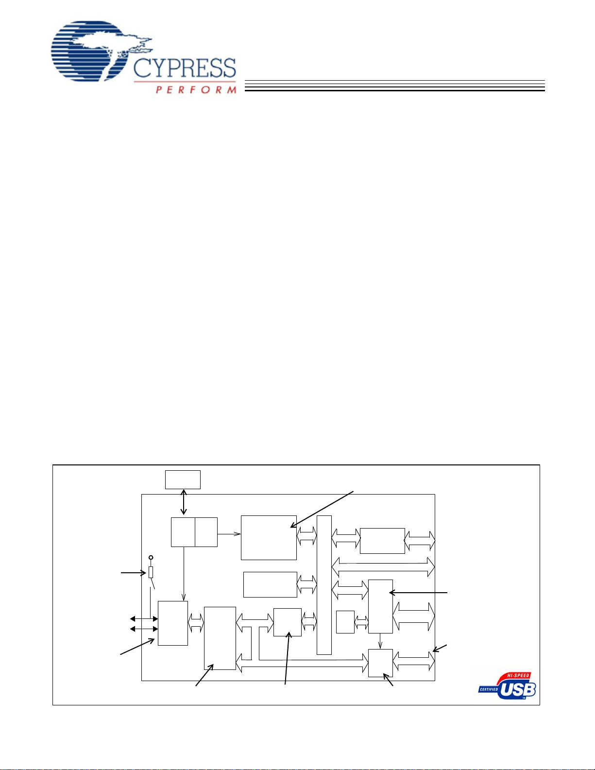
Block Diagram
24 MHz
Ext. Xtal
High-performance,
enhanced 8051 core
with low power options
NX2LP-Flex
/0.5
x20
/1.0
PLL
/2.0
CY
Smart
USB
1.1/2.0
Engine
Connected for
full-speed USB
Integrated full- and
high-speed XCVR
D+
D–
V
CC
1.5k
USB
2.0
XCVR
Enhanced USB core
simplifies 8051 code
Cypress Semiconductor Corporation • 198 Champion Court • San Jose, CA 95134-1709 • 408-943-2600
Document #: 001-04247 Rev. *D Revised September 21, 2006
8051 Core
12/24/48 MHz,
four clocks/cycle
NAND
Boot Logic
(ROM)
15 kB
RAM
‘Soft Configuration’ enables
easy firmware changes
I2C
Master
Additional I/Os
GPIF
ECC
Address (16)/Data Bus (8)
4 kB
FIFO
FIFO and USB endpoint memory
(master or slave modes)
RDY (2)
CTL (3)
8/16
General Programmable
I/F to ASIC/DSP or bus
standards such as 8-bit
NAND, EPP, etc.
Up to 96 MB/s burst rate
[+] Feedback
Page 2

CY7C68033/CY7C68034
Default NAND Firmware Features
Because the NX2LP-Flex™ is intended for NAND
Flash-based USB mass storage applications, a default
firmware image is included in the development kit with the
following features:
• High (480-Mbps) or full (12-Mbps) speed USB support
• Both common NAND page sizes supported
— 512 bytes for up to 1 Gb capacity
— 2K bytes for up to 8 Gb capacity
• 12 configurable general-purpose I/O (GPIO) pins
— 2 dedicated chip enable (CE#) pins
— 6 configurab le CE#/GPIO pins
• Up to 8 NAND Flash single-device (single-die) chips are
supported
• Up to 4 NAND Flash dual-device (dual-die) chips are
supported
• Compile option allows unused CE# pins to be configured as GPIOs
— 4 dedicated GPIO pins
• Industry standard ECC NAND Flash correction
— 1-bit per 256-bit correction
— 2-bit error detection
• Industry standard (SmartMedia) page management for
wear leveling algorithm, bad block handling, and Physical
to Logical management.
• 8-bit NAND Flash interface support
• Support for 30-ns, 50-ns, and 100-ns NAND Flash timing
• Complies with the USB Mass Storage Class Specification
revision 1.0
The default firmware image implements a USB 2.0 NAND
Flash controller. This controller adheres to the Mass Storage
Class Bulk-Only Transport Specification. The USB port of the
NX2LP-Flex is connected to a host computer directly or via the
downstream port of a USB hub. Host software issues
commands and data to the NX2LP-Flex and receives status
and data from the NX2LP-Flex using standard USB protocol.
The default firmware image supports industry leading 8-bit
NAND Flash interfaces and both common NAND page sizes
of 512 and 2k bytes. Up to eight chip enable p ins allow the
NX2LP-Flex to be connected to up to eight single- or four
dual-die NAND Flash chips.
Complete source code and documentation for the default
firmware image are included in the NX2LP-Flex development
kit to enable customization for meeting design requirements.
Additionally, compile options for the default firmware allow for
quick configuration of some features to decrease design effort
and increase time-to-market advantages.
Overview
Cypress Semiconductor Corporation’s (Cypress’s) EZ-USB
NX2LP-Flex (CY7C68033/CY7C68034) is a firmware-based,
programmable version of the EZ-USB NX2LP™
(CY7C68023/CY7C68024), which is a fixed-function,
low-power USB 2.0 NAND Flash controller. By integrating the
USB 2.0 transceiver, serial interface engine (SIE), enhanced
8051 microcontroller, and a programmable peripheral
interface in a single chip, Cypress has created a very
cost-effective solution that enables feature-rich NAND
Flash-based applications.
The ingenious architecture of NX2LP-Flex results in USB data
transfer rates of over 53 Mbytes per second, the
maximum-allowable USB 2.0 bandwidth, while still using a
low-cost 8051 microcontroller in a small 56-pin QFN package.
Because it incorporates the USB 2.0 transceiver, the
NX2LP-Flex is more economical, providing a smaller footprint
solution than external USB 2.0 SIE or transceiver implementations. With EZ-USB NX2LP-Flex, the Cypress Smart SIE
handles most of the USB 1.1 and 2.0 protocol, freeing the
embedded microcontroller for application-specific functions
and decreasing development time while ensuring USB
compatibility.
The General Programmable Interface (GPIF) and
Master/Slave Endpoint FIFO (8- or 16-bit data bus) provide an
easy and glueless interface to popular interfaces such as
UTOPIA, EPP, I
2
C, PCMCIA, and most DSP processors.
Applications
The NX2LP-Flex allows designers to add extra functionality to
basic NAND Flash mass storage designs, or to interface them
with other peripheral devices. Applications may include:
• NAND Flash-based GPS devices
• NAND Flash-based DVB video capture devices
• Wireless pointer/presenter tools with NAND Flash storage
• NAND Flash-based MPEG/TV conversion devices
• Legacy conversion devices with NAND Flash storage
• NAND Flash-based cameras
• NAND Flash mass storage device with biometric (e.g.,
fingerprint) security
• Home PNA devices with NAND Flash storage
• Wireless LAN with NAND Flash storage
• NAND Flash-based MP3 players
• LAN networking with NAND Flash storage
Document #: 001-04247 Rev. *D Page 2 of 33
[+] Feedback
Page 3

CY7C68033/CY7C68034
Figure 1. Example DVB Block Diagram
NAND-Based
DVB Unit
LCD
D+/-
Audio / Video I/O
Buttons
I/O
NX2LP-
Flex
DVB
Decoder
CTL
CE[7:0]
I/O I/O
NAND Bank(s)
I/O
Figure 2. Example GPS Block Diagram
NAND-Based
GPS Unit
LCD
D+/-
Buttons
I/O
NX2LP-
Flex
CTL
CE[7:0]
I/O I/O
NAND Bank(s)
I/O
8051 Microprocessor
The 8051 microprocessor embedded in the NX2LP-Flex has
256 bytes of register RAM, an expanded interrupt system and
three timer/counters.
8051 Clock Frequency
NX2LP-Flex has an on-chip oscillator circuit that uses an
external 24-MHz (±100-ppm) crystal with the following characteristics:
• Parallel resonant
• Fundamental mode
• 500-μW drive level
• 12-pF (5% tolerance) load capacitors.
An on-chip PLL multiplies the 24-MHz oscillator up to
480 MHz, as required by the transceiver/PHY, and internal
counters divide it down for use as the 8051 clock. The default
8051 clock frequency is 12 MHz. The clock frequency of the
8051 can be changed by the 8051 through the CPUCS
register, dynamically
Figure 3. Crystal Configuration.
24 MHz
C1
12 pf
C2
12 pf
20 × PLL
GPS
The “Reference Designs” section of the Cypress web site
provides additional tools for typical USB 2.0 applications. Each
reference design comes complete with firmware source and
object code, schematics, and documentation. Please visit
http://www.cypress.com for more information.
Functional Overview
USB Signaling Speed
NX2LP-Flex operates at two of the three rates defined in the
USB Specification Revision 2.0, dated April 27, 2000:
• Full speed, with a signaling bit rate of 12 Mbps
• High speed, with a signaling bit rate of 480 Mbps.
NX2LP-Flex does not support the low-speed signaling mode
of 1.5 Mbps.
12-pF capacitor values assumes a trace capacitance
of 3 pF per side on a four-layer FR4 PCA
Special Function Registers
Certain 8051 SFR addresses are populated to provide fast
access to critical NX2LP-Flex functions. These SFR additions
are shown in Table 1. Bold type indicates non-standard,
enhanced 8051 registers. The two SFR rows that end with ‘0’
and ‘8’ contain bit-addressable registers. The four I/O ports
A–D use the SFR addresses used in the standard 8051 for
ports 0–3, which are not implemented in NX2LP-Flex.
Because of the faster and more efficient SFR addressing, the
NX2LP-Flex I/O ports are not addressable in external RAM
space (using the MOVX instruction).
2
I
C Bus
2
NX2LP supports the I
SCL and SDA pins have open-drain outputs and hysteresis
inputs. These signals must be pulled up to 3.3V , even if no I
device is connected. The I
C bus as a master only at 100-/400-kHz.
2
2
C bus is disabled at startup and
only available for use after the initial NAND access.
C
Document #: 001-04247 Rev. *D Page 3 of 33
[+] Feedback
Page 4

CY7C68033/CY7C68034
Table 1. Special Function Registers
x8x 9x Ax Bx CxDxExFx
0
1SP EXIF INT2CLR IOE SBUF1
2DPL0 MPAGE
3DPH0
4 DPL1 OEC
5 DPH1
6 DPS
7PCON
8 TCON SCON0 IE IP T2CON EICON EIE EIP
9 TMOD SBUF0
ATL0AUTOPTRH1 EP2468STAT EP01STAT RCAP2L
BTL1AUTOPTRL1 EP24FIFOFLGS GPIFTRIG RCAP2H
CTH0RESERVED EP68FIFOFLGS TL2
DTH1AUTOPTRH2 GPIFSGLDATH TH2
E CKCON AUTOPTRL2 GPIFSGLDA TLX
F RESERVED AUTOPTRSET-UP GPIFSGLDATLNOX
IOA IOB IOC IOD SCON1 PSW ACC B
INT4CLR OEA
OEB
OED
OEE
Buses
The NX2LP-Flex features an 8- or 16-bit ‘FIFO’ bidirectional
data bus, multiplexed on I/O port s B and D.
The default firmware image implements an 8-bit data bus in
GPIF Master mode. It is recommended that additional interfaces added to the default firmware image use thi s 8-bit data
bus.
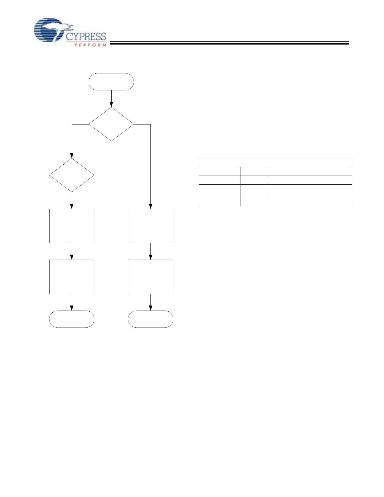
Enumeration
During the start-up sequence, internal logic checks for the
presence of NAND Flash with valid firmware. If valid firmware
is found, the NX2LP-Flex loads it and operates accord ing to
the firmware. If no NAND Flash is detected, or if no valid
firmware is found, the NX2LP-Flex uses the default values
from internal ROM space for manufacturing mode operation.
The two modes of operation are described in the section
”Normal Operation Mode” on page 5 and ”Manufacturing
Mode” on page 5.
Document #: 001-04247 Rev. *D Page 4 of 33
[+] Feedback
Page 5
CY7C68033/CY7C68034
Figure 4. NX2LP-Flex Enumeration Sequence
Start-up
Yes No
NAND Flash
Programmed?
Yes
Load Firmware
From NAND
NAND Flash
Present?
No
Load Default
Descriptors and
Configuration Data
values stored in ROM space. The default silicon ID values
should only be used for development purposes. Cypress
requires designers to use their own Vendor ID for final
products. A Vendor ID is obtained through registration with the
USB Implementor’s Forum (USB-IF). Also, if the NX2LP-Flex
is used as a mass storage class device, a unique USB serial
number is required for each device in order to comply with the
USB Mass Storage class specification.
Cypress provides all the software tools and drivers necessary
for properly programming and testing the NX2LP-Flex. Please
refer to the documentation in the development kit for more
information on these topics.
Table 2. Default Silicon ID Values
Default VID/PID/DID
Vendor ID 0x04B4 Cypress Semiconductor
Product ID 0x8613 EZ-USB
®
Default
Device release 0xAnnn Depends on chip revision
(nnn = chip revision, where first
silicon = 001)
ReNumeration™
Cypress’s ReNumeration™ feature is used in conjunction with
the NX2LP-Flex manufacturing software tools to enable
first-time NAND programming. It is only available when used
in conjunction with the NX2LP-Flex Manufacturing tools, and
is not enabled during normal operation.
Enumerate
According To
Firmware
Normal Operation
Mode
Enumerate As
Unprogrammed
NX2LP-Flex
Manufacturing
Mode
Normal Operation Mode
In Normal Operation Mode, the NX2LP-Flex behaves as a
USB 2.0 Mass Storage Class NAND Flash controller. This
includes all typical USB device states (powered, configured,
etc.). The USB descriptors are returned accordi n g to th e d ata
stored in the configuration data memory area. Normal read
and write access to the NAND Flash is available in this mode.
Manufacturing Mode
In Manufacturing Mode, the NX2LP-Flex enumerates using
the default descriptors and configuration data that are stored
in internal ROM space. This mode allows for first-time
programming of the configuration data memory area, as well
as board-level manufacturing tests.
Default Silicon ID Values
To facilitate proper USB enumeration when no programmed
NAND Flash is present, the NX2LP-Flex has default silicon ID
Bus-powered Applications
The NX2LP-Flex fully supports bus-powered designs by
enumerating with less than 100 mA, as required by the USB
2.0 specification.
Interrupt System
INT2 Interrupt Request and Enable Registers
NX2LP-Flex implements an autovector feature for INT2 and
INT4. There are 27 INT2 (USB) vectors, and 14 INT4
(FIFO/GPIF) vectors. See the EZ-USB Technical Reference
Manual (TRM) for more details.
USB-Interrupt Autovectors
The main USB interrupt is shared by 27 interrupt sources. To
save the code and processing time that normally would be
required to identify the individual USB interrupt source, the
NX2LP-Flex provides a second level of interrupt vectoring,
called Autovectoring. When a USB interrupt is asserted, the
NX2LP-Flex pushes the program counter onto its stack then
jumps to address 0x0500, where it expects to find a ‘jump’
instruction to the USB Interrupt service routin e .
Developers familiar with Cypress’s programmable USB
devices should note that these interrupt vector values differ
from those used in other EZ-USB microcontrollers. This is due
to the additional NAND boot logic that is present in the
NX2LP-Flex ROM space. Also, these values are fixed and
cannot be changed in the firmware.
Document #: 001-04247 Rev. *D Page 5 of 33
[+] Feedback
Page 6

CY7C68033/CY7C68034
Table 3. INT2 USB Interrupts
USB INTERRUPT TABLE FOR INT2
Priority INT2VEC Value Source Notes
1 0x500 SUDAV Setup Data Available
2 0x504 SOF Start of Frame (or microframe)
3 0x508 SUTOK Setup Token Received
4 0x50C SUSPEND USB Suspend request
5 0x510 USB RESET Bus reset
6 0x514 HISPEED Entered high speed operation
7 0x518 EP0ACK NX2LP ACK’d the CONTROL Handshake
8 0x51C Reserved
9 0x520 EP0-IN EP0-IN ready to be loaded with data
10 0x524 EP0-OUT EP0-OUT has USB data
11 0x528 EP1-IN EP1-IN ready to be loaded with data
12 0x52C EP1-OUT EP1-OUT has USB data
13 0x530 EP2 IN: buffer available. OUT: buffer has data
14 0x534 EP4 IN: buffer available. OUT: buffer has data
15 0x538 EP6 IN: buffer available. OUT: buffer has data
16 0x53C EP8 IN: buffer available. OUT: buffer has data
17 0x540 IBN IN-Bulk-NAK (any IN endpoint)
18 0x544 Reserved
19 0x548 EP0PING EP0 OUT was Pinged and it NAK’d
20 0x54C EP1PING EP1 OUT was Pinged and it NAK’d
21 0x550 EP2PING EP2 OUT was Pinged and it NAK’d
22 0x554 EP4PING EP4 OUT was Pinged and it NAK’d
23 0x558 EP6PING EP6 OUT was Pinged and it NAK’d
24 0x55C EP8PING EP8 OUT was Pinged and it NAK’d
25 0x560 ERRLIMIT Bus errors exceeded the programmed limit
26 0x564 Reserved
27 0x568 Reserved
28 0x56C Reserved
29 0x570 EP2ISOERR ISO EP2 OUT PID sequence error
30 0x574 EP4ISOERR ISO EP4 OUT PID sequence error
31 0x578 EP6ISOERR ISO EP6 OUT PID sequence error
32 0x57C EP8ISOERR ISO EP8 OUT PID sequence error
If Autovectoring is enabled (AV2EN = 1 in the INTSET-UP
register), the NX2LP-Flex substitutes its INT2VEC byte.
Therefore, if the high byte (‘page’) of a jump-table address is
preloaded at location 0x544, the automatically-inserted
INT2VEC byte at 0x545 will direct the jump to the correct
address out of the 27 addresses within the page.
Document #: 001-04247 Rev. *D Page 6 of 33
FIFO/GPIF Interrupt (INT4)
Just as the USB Interrupt is shared among 27 individual
USB-interrupt sources, the FIFO/GPIF interrupt is shared
among 14 individual FIFO/GPIF sources. The FIFO/GPIF
Interrupt, like the USB Interrupt, can employ autovectoring.
Table 4 shows the priority and INT4VEC values for the 14
FIFO/GPIF interrupt sources.
[+] Feedback
Page 7
CY7C68033/CY7C68034
Ta bl e 4. Individual FIFO/GPIF Interrupt Sources
Priority INT4VEC Value Source Notes
1 0x580 EP2PF Endpoint 2 Programmable Flag
2 0x584 EP4PF Endpoint 4 Programmable Flag
3 0x588 EP6PF Endpoint 6 Programmable Flag
4 0x58C EP8PF Endpoint 8 Programmable Flag
5 0x590 EP2EF Endpoint 2 Empty Flag
6 0x594 EP4EF Endpoint 4 Empty Flag
7 0x598 EP6EF Endpoint 6 Empty Flag
8 0x59C EP8EF Endpoint 8 Empty Flag
9 0x5A0 EP2FF Endpoint 2 Full Flag
10 0x5A4 EP4FF Endpoint 4 Full Flag
11 0x5A8 EP6FF Endpoint 6 Full Flag
12 0x5AC EP8FF Endpoint 8 Full Flag
13 0x5B0 GPIFDONE GPIF Operation Complete
14 0x5B4 GPIFWF GPIF Waveform
If Autovectoring is enabled (AV4EN = 1 in the INTSET-UP
register), the NX2LP-Flex substitutes its INT4VEC byte.
Therefore, if the high byte (‘page’) of a jump-table address is
preloaded at location 0x554, the automatically-inserted
INT4VEC byte at 0x555 will direct the jump to the correct
address out of the 14 addresses within the page. When the
ISR occurs, the NX2LP-Flex pushes the program counter onto
its stack then jumps to address 0x553, where it expects to find
a ‘jump’ instruction to the ISR Interrupt service routine.
Reset and Wakeup
Reset Pin
The input pin RESET#, will reset the NX2LP-Flex when
asserted. This pin has hysteresis and is active LOW. When a
crystal is used as the clock source for the NX2LP-Flex, the
Figure 5. Reset Timing Plots
RESET#
V
IL
3.3V
3.0V
V
CC
0V
T
RESET
Power-on Reset
reset period must allow for the stabilization of the crystal and
the PLL. This reset period should be approximately 5 ms after
V
has reached 3.0V. If the crystal input pin is driven by a
CC
clock signal, the internal PLL stabilizes in 200 μs after V
reached 3.0V
[1]
. Figure 5 shows a power-on reset condition
CC
and a reset applied during operation. A power-on reset is
defined as the time reset is asserted while power is being
applied to the circuit. A powered reset is defined to be when
the NX2LP-Flex has previously been powered on and
operating and the RESET# pin is asserted.
Cypress provides an application note which describes and
recommends power on reset implementation and can be found
on the Cypress web site. For more information on reset implementation for the EZ-USB family of products visit the
http://www.cypress.com website.
RESET#
V
IL
3.3V
V
CC
0V
T
RESET
Powered Reset
has
Note
1. If the external clock is powered at the same time as the CY7C68033/CY7C68034 and has a stabilization wait period, it must be added to the 200 μs.
Document #: 001-04247 Rev. *D Page 7 of 33
[+] Feedback
Page 8

CY7C68033/CY7C68034
Table 5. Reset Timing Values
Condition T
RESET
Power-on Reset with crystal 5 ms
Power-on Reset with external
200 μs + Clock stability time
clock source
Powered Reset 200 μs
Wakeup Pins
The 8051 puts itself and the rest of the chip into a power-down
mode by setting PCON.0 = 1. This stops the oscillator and
PLL. When WAKEUP is asserted by external logic, the oscillator restarts, after the PLL stabilizes, and then the 8051
receives a wakeup interrupt. This applies whether or not
NX2LP-Flex is connected to the USB.
The NX2LP-Flex exits the power-down (USB suspend) state
using one of the following methods:
• USB bus activity (if D+/D– lines are left floating, noise on
these lines may indicate activity to the NX 2L P-F l ex an d
initiate a wakeup).
• External logic asserts the WAKEUP pin
• External logic asserts the PA3/WU2 pin.
The second wakeup pin, WU2, can also be configured as a
general purpose I/O pin. This allows a simple external R-C
network to be used as a periodic wakeup source. Note that
WAKEUP is, by default, active LOW.
Figure 6. Internal Code Memory
FFFF
E200
E1FF
E000
*SUDPTR, USB download, NAND boot access
Register Addresses
Figure 7. Internal Register Addresses
7.5 kBytes
USB registers
and 4 kBytes
FIFO buffers
(RD#, WR#)
512 Bytes RAM Data
(RD#, WR#)*
3FFF
15 kBytes RAM
Code and Data
(PSEN#, RD#,
0500
1 kbyte ROM
0000
WR#)*
Program/Data RAM
Internal ROM/RAM Size
The NX2LP-Flex has 1 kBytes ROM and 15 kBytes of internal
program/data RAM, where PSEN#/RD# signals are internally
ORed to allow the 8051 to access it as both program and data
memory. No USB control registers appear in this space.
Internal Code Memory
This mode implements the internal block of RAM (starting at
0x0500) as combined code and data memory, as shown in
Figure 6, below.
Only the internal and scratch pad RAM spaces have the
following access:
• USB download (only supported by the Cypress Manufacturing Tool)
• Setup data pointer
• NAND boot access.
FFFF
F000
EFFF
E800
E7FF
E7C0
E7BF
E780
E77F
E740
E73F
E700
E6FF
E500
E4FF
E480
E47F
E400
E3FF
E200
E1FF
E000
4 KBytes EP2-EP8
(8 x 512)
2 KBytes RESERVED
64 Bytes EP1IN
64 Bytes EP1OUT
64 Bytes EP0 IN/OUT
64 Bytes RESERVED
8051 Addressable Registers
Reserved (128)
128 bytes GPIF Waveforms
Reserved (512)
512 bytes
8051 xdata RAM
buffers
(512)
Document #: 001-04247 Rev. *D Page 8 of 33
[+] Feedback
Page 9
CY7C68033/CY7C68034
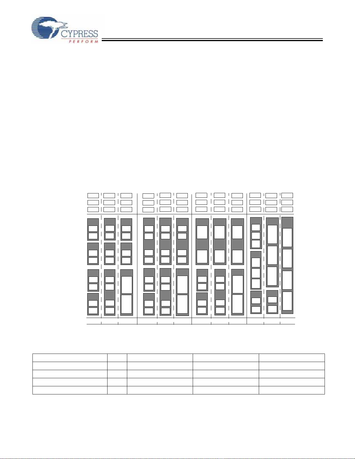
Endpoint RAM
Size
• 3 × 64 bytes (Endpoints 0 and 1)
• 8 × 512 bytes (Endpoints 2, 4, 6, 8)
Organization
• EP0
— Bidirectional endpoint zero, 64-byte buffer
• EP1IN, EP1OUT
— 64-byte buffers, bulk or interrupt
• EP2,4,6,8
— Eight 512-byte buffers, bulk, interrupt, or isochronous.
— EP4 and EP8 can be double buffered, while EP2 and 6
can be either double, triple, or quad buffered.
For high-speed endpoint configuration options, see Figure 8.
Figure 8. Endpoint Configuration
EP0 IN&OUT
EP1 IN
EP1 OUT
64
64
64
EP2
512
512
EP4
512
512
EP6
512
512
EP8
512
512
1
64
64
64
EP2
512
512
EP4
512
512
EP6
512
512
512
512
2
64
64
64
EP2
512
512
EP4
512
512
EP6
1024
1024
3
EP2
512
512
512
512
EP6
512
512
EP8
512
512
64
64
64
64
64
64
EP2
512
512
512
512
EP6
512
512
512
512
4
5
Setup Data Buffer
A separate 8-byte buffer at 0xE6B8-0xE6BF holds the setup
data from a CONTROL transfer.
Endpoint Configurations (High-speed Mode)
Endpoints 0 and 1 are the same for every configuration.
Endpoint 0 is the only CONTROL endpoint, and endpoint 1 can
be either BULK or INTERRUPT. The endpoint buffers can be
configured in any 1 of the 12 configurations shown in the
vertical columns. When operating in full-speed BULK mode,
only the first 64 bytes of each buffer are used. For example, in
high-speed the max packet size is 512 bytes, but in full-speed
it is 64 bytes. Even though a buffer is configured to be a 512
byte buffer, in full-speed only the first 64 bytes are used. The
unused endpoint buffer space is not available for other operations. An example endpoint configuration would be:
EP2–1024 double buffered; EP6–512 quad buffered
(column 8 in Figure 8).
64
64
64
EP2
512
512
512
512
EP6
1024
1024
6
64
64
64
EP2
1024
1024
EP6
512
512
EP8
512
512
64
64
64
EP2
1024
1024
EP6
512
512
512
512
7
64
64
64
EP2
1024
1024
EP6
1024
1024
8
64
64
64
EP2
512
512
512
EP6
512
512
512
EP8
512
512
10
9
64
64
64
EP2
1024
1024
1024
1024
EP8
512
512
11
64
64
64
EP2
1024
1024
1024
1024
12
Default Full-Speed Alternate Settings
Table 6. Default Full-Speed Alternate Settings
[2, 3]
Alternate Setting 0 1 2 3
ep0 64 64 64 64
ep1out 0 64 bulk 64 int 64 int
ep1in 0 64 bulk 64 int 64 int
ep2 0 64 bulk out (2×) 64 int out (2×) 64 iso out (2×)
Notes
2. ‘0’ means ‘not implemented.’
3. ‘2×’ means ‘double buffered.’
Document #: 001-04247 Rev. *D Page 9 of 33
[+] Feedback
Page 10

CY7C68033/CY7C68034
Table 6. Default Full-Speed Alternate Settings
[2, 3]
(continued)
ep4 0 64 bulk out (2×) 64 bulk out (2×) 64 bulk out (2×)
ep6 0 64 bulk in (2×) 64 int in (2×) 64 iso in (2×)
ep8 0 64 bulk in (2×) 64 bulk in (2×) 64 bulk in (2×)
Default High-Speed Alternate Settings
Table 7. Default High-Speed Alternate Settings
[2, 3]
Alternate Setting 0 1 2 3
ep0 64 64 64 64
ep1out 0 512 bulk
ep1in 0 512 bulk
[4]
[4]
64 int 64 int
64 int 64 int
ep2 0 512 bulk out (2×) 512 int out (2×) 512 iso out (2×)
ep4 0 512 bulk out (2×) 512 bulk out (2×) 512 bulk out (2×)
ep6 0 512 bulk in (2×) 512 int in (2×) 512 iso in (2×)
ep8 0 512 bulk in (2×) 512 bulk in (2×) 5 12 bulk in (2×)
External FIFO Interface
Architecture
The NX2LP-Flex slave FIFO architecture has eight 512-byte
blocks in the endpoint RAM that directly serve as FIFO
memories, and are controlled by FIFO control signals (such as
SLCS#, SLRD, SLWR, SLOE, PKTEND, and flags).
In operation, some of the eight RAM blocks fill or empty from
the SIE, while the others are connected to the I/O transfer
logic. The transfer logic takes two forms, the GPIF for internally
generated control signals, or the slave FIFO interface for
externally controlled transfers.
(IFCLK), at a rate that transfers data up to 96 Megabytes/s
(48-MHz IFCLK with 16-bit interface).
In Slave (S) mode, the NX2LP-Flex accepts an internally
derived clock (IFCLK, max. frequency 48 MHz) and SLCS#,
SLRD, SLWR, SLOE, PKTEND signals from external logic.
Each endpoint can individually be selected for byte or word
operation by an internal configuration bit, and a Slave F IFO
Output Enable signal SLOE enables data of the selected
width. External logic must ensure that the output enable signal
is inactive when writing data to a slave FIFO. The slave
interface must operate asynchronously, where the SLRD and
SLWR signals act directly as strobes, rather than a clock
qualifier as in a synchronous mode. The signals SLRD, SLWR,
Master/Slave Control Signals
The NX2LP-Flex endpoint FIFOS are implemented as eight
physically distinct 256x16 RAM blocks. The 8051/SIE can
switch any of the RAM blocks between two domains, the USB
(SIE) domain and the 8051-I/O Unit domain. This switching is
done virtually instantaneously, giving essentially zero transfer
time between ‘USB FIFOS’ and ‘Slave FIFOS.’ Since they are
physically the same memory, no bytes are actually transferred
between buffers.
At any given time, some RAM blocks are filling/emptying with
USB data under SIE control, while other RAM blocks are
available to the 8051 and/or the I/O control unit. The RAM
blocks operate as single-port in the USB domain, and
dual-port in the 8051-I/O domain. The blocks can be
configured as single, double, triple, or quad buffered as previously shown.
The I/O control unit implements either an internal-master (M
for master) or external-master (S for Slave) interface.
In Master (M) mode, the GPIF internally controls
FIFOADR[1:0] to select a FIFO. The two RDY pins can be
used as flag inputs from an external FIFO or other logic if
desired. The GPIF can be run from an internally derived clock
SLOE and PKTEND are gated by the signal SLCS#.
GPIF and FIFO Clock Rates
An 8051 register bit selects one of two frequencies for the
internally supplied interface clock: 30 MHz and 48 MHz. A bit
within the IFCONFIG register will invert the IFCLK signal.
The default NAND firmware image implements a 48-MHz
internally supplied interface clock. The NAND boot logic uses
the same configuration to implement 100-ns timing on the
NAND bus to support proper detection of all NAND Flash
types.
GPIF
The GPIF is a flexible 8- or 16-bit parallel interface driven by a
user-programmable finite state machine. It allows the
NX2LP-Flex to perform local bus mastering, and can
implement a wide variety of protocols such as 8-bit NAND
interface, printer parallel port, and Utopia. The default NAND
firmware and boot logic utilizes GPIF functionality to interface
with NAND Flash.
The GPIF on the NX2LP-Flex features three programmable
control outputs (CTL) and two general-purpose ready inputs
(RDY). The GPIF data bus width can be 8 or 16 bits. Because
Note
4. Even though these buffers are 64 bytes, they are reported as 512 for USB 2.0 compliance. The user must never transfer packets larger than 64 bytes to EP1.
Document #: 001-04247 Rev. *D Page 10 of 33
[+] Feedback
Page 11

CY7C68033/CY7C68034
the default NAND firmware image implements an 8-bit data
bus and up to 8 chip enable pins on the GPIF ports, it is recommended that designs based upon the default firmware image
use an 8-bit data bus as well.
Each GPIF vector defines the state of the control outputs, and
determines what state a ready input (or multiple inputs) must
be before proceeding. The GPIF vector can be programmed
to advance a FIFO to the next data value, advance an address,
etc. A sequence of the GPIF vectors make up a single
waveform that will be executed to perform the desired data
move between the NX2LP-Flex and the external device.
Three Control OUT Signals
The NX2LP-Flex exposes three control signals, CTL[2:0].
CTLx waveform edges can be programmed to make transitions as fast as once per clock (20.8 ns using a 48-MHz clock).
Two Ready IN Signals
The 8051 programs the GPIF unit to test the RDY pins for
GPIF branching. The 56-pin package brings out two signals,
RDY[1:0].
Long Transfer Mode
In GPIF Master mode, the 8051 appropriately sets GPIF transaction count registers (GPIFTCB3, GPIFTCB2, GPIFTCB1, or
GPIFTCB0) for unattended transfers of up to 2
32
transactions.
The GPIF automatically throttles data flow to prevent under- or
over-flow until the full number of requested transactions
complete. The GPIF decrements the value in these registers
to represent the current status of the transaction.
ECC Generation
[5]
The NX2LP-Flex can calculate ECCs (Error-Correcting
Codes) on data that passes across its GPIF or Slave FIFO
interfaces. There are two ECC configurations:
• Two ECCs, each calculated over 256 bytes (SmartMedia
Standard)
• One ECC calculated over 512 bytes.
The two ECC configurations described below are selected by
the ECCM bit. The ECC can correct any one-bit error or detect
any two-bit error.
ECCM = 0
Two 3-byte ECCs, each calculated over a 256-byte block of
data. This configuration conforms to the SmartMedia Standard
and is used by both the NAND boot logic and default NAND
firmware image.
When any value is written to ECCRESET and data is then
passed across the GPIF or Slave FIFO interface, the ECC for
the first 256 bytes of data will be calculated and stored in
ECC1. The ECC for the next 256 bytes of data will be stored
in ECC2. After the second ECC is calculated, the values in the
ECCx registers will not change until ECCRESET is written
again, even if more data is subsequently passed across the
interface.
ECCM = 1
One 3-byte ECC calculated over a 512-byte block of data.
When any value is written to ECCRESET and data is then
passed across the GPIF or Slave FIFO interface, the ECC for
the first 512 bytes of data will be calculated and stored in
ECC1; ECC2 is unused. After the ECC is calculated, the value
in ECC1 will not change until ECCRESET is written again,
even if more data is subsequently passed across the interface
Autopointer Access
NX2LP-Flex provides two identical autopointers. They are
similar to the internal 8051 data pointers, but with an additional
feature: they can optionally increment after every memory
access. Also, the autopointers can point to any NX2LP-Flex
register or endpoint buffer space.
2
I
C Controller
NX2LP has one I2C port that the 8051, once running uses to
control external I
mode only. The I
2
C devices. The I2C port operates in master
2
C post is disabled at startup and only
available for use after the initial NAND access.
2
I
C Port Pins
2
The I
C pins SCL and SDA must have external 2.2-kΩ pull-up
resistors even if no EEPROM is connected to the NX2LP.
2
I
C Interface General-Purpose Access
The 8051 can control peripherals connected to the I
using the I
master control only and is never an I
2
CTL and I2DATA registers. NX2LP provides I2C
2
C slave.
2
C bus
Note
5. T o use the ECC logic, the GPIF or Slave FIFO interface must be configured for byte-wide operation.
Document #: 001-04247 Rev. *D Page 11 of 33
[+] Feedback
Page 12

CY7C68033/CY7C68034
Pin Assignments
Figure 9 and Figure 10 identify all signals for the 56-pin
NX2LP-Flex package.
Three modes of operation are available for the NX2LP-Flex:
Port mode, GPIF Master mode, and Slave FIFO mode. These
modes define the signals on the right edge of each column in
Figure 9. The right-most column details the signal functionality
Figure 9. Port and Signal Mapping
Port GPIF Master Slave FIFO
↔ FD[15]
PD7
↔ FD[14]
PD6
↔ FD[13]
PD5
↔ FD[12]
PD4
↔ FD[11]
PD3
↔ FD[10]
PD2
↔ FD[9]
PD1
↔ FD[8]
PD0
↔ FD[7]
PB7
↔ FD[6]
PB6
↔ FD[5]
XTALIN
XTALOUT
RESET#
WAKEUP#
SCL
SDATA
DPLUS
DMINUS
PB5
PB4
PB3
PB2
PB1
PB0
PA7
PA6
PA5
PA4
WU2/PA3
PA2
INT1#/PA1
INTO#/PA0
GPIO8
GPIO9
↔ FD[4]
↔ FD[3]
↔ FD[2]
↔ FD[1]
↔ FD[0]
→ RDY0
→ RDY1
← CTL0
← CTL1
← CTL2
↔ PA7
↔ PA6
↔ PA5
↔ PA4
↔ PA3/WU2
↔ PA2
↔ PA1/INT1#
↔ PA0/INT0#
↔ GPIO8
← GPIO9
from the default NAND firmware image, which actually utilizes
GPIF Master mode. The signals on the left edge of the ‘Port’
column are common to all modes of the NX2LP-Flex. The
8051 selects the interface mode using the IFCONFIG[1:0]
register bits. Port mode is the power-on default configuration.
Figure 10 details the pinout of the 56-pin package and lists pin
names for all modes of operation. Pin names with an asterisk
(*) feature programmable polarity.
Default NAND
Firmware Use
↔ FD[15]
↔ FD[14]
↔ FD[13]
↔ FD[12]
↔ FD[11]
↔ FD[10]
↔ FD[9]
↔ FD[8]
↔ FD[7]
↔ FD[6]
↔ FD[5]
↔ FD[4]
↔ FD[3]
↔ FD[2]
↔ FD[1]
↔ FD[0]
→ SLRD
→ SLWR
← FLAGA
← FLAGB
← FLAGC
↔ FLAGD/SLCS#/PA7
↔ PKTEND
← FIFOADR1
↔ FIFOADR0
← PA3/WU2
← SLOE
← PA1/INT1#
↔ PA0/INT0#
↔ GPIO8
← GPIO9
↔ CE7#/GPIO7
↔ CE6#/GPIO6
↔ CE5#/GPIO5
↔ CE4#/GPIO4
↔ CE3#/GPIO3
↔ CE2#/GPIO2
↔ CE1#
↔ CE0#
↔ DD7
↔ DD6
↔ DD5
↔ DD4
↔ DD3
↔ DD2
↔ DD1
↔ DD0
→ R_B1#
→ R_B2#
← WE#
← RE0#
← RE1#
← GPIO1
← GPIO0
← WP_SW#
← WP_NF#
← LED2#
→ LED1#
↔ ALE
↔ CLE
↔ GPIO8
← GPIO9
Document #: 001-04247 Rev. *D Page 12 of 33
[+] Feedback
Page 13

CY7C68033/CY7C68034
Figure 10. CY7C68033/CY7C68034 56-pin QFN Pin Assignment
RDY0/*SLRD
RDY1/*SLWR
AVCC
XTALOUT
XTALIN
AGND
AVCC
DPLUS
DMINUS
AGND
VCC
GND
10
11
12
PD5/FD13
PD6/FD14
PD7/FD15
PD2/FD10
PD3/FD11
PD4/FD12
PD1/FD9
*WAKEUP
PD0/FD8
GPIO9
GND
VCC
55
56
1
2
3
4
5
6
7
8
9
GND
48
49
50
51
52
53
54
CY7C68033/CY7C68034
56-pin QFN
47
46
45
44
VCC
43
RESET#
42
GND
41
PA7/*FLAGD/SLCS#
40
PA6/*PKTEND
39
PA5/FIFOADR1
38
PA4/FIFOADR0
37
PA3/*WU2
36
PA2/*SLOE
35
PA1/INT1#
34
PA0/INT0#
33
VCC
32
CTL2/*FLAGC
31
GPIO8
RESERVED#
13
14
15
SCL
16
SDATA
17
VCC
19
18
PB1/FD1
PB0/FD0
21
20
PB3/FD3
PB2/FD2
23
22
PB5/FD5
PB4/FD4
25
24
PB7/FD7
PB6/FD6
26
GND
27
VCC
28
GND
CTL1/*FLAGB
30
29
CTL0/*FLAGA
Document #: 001-04247 Rev. *D Page 13 of 33
[+] Feedback
Page 14

n
CY7C68033/CY7C68034
Table 8. NX2LP-Flex Pin Descriptions
56 QFN
Pin
Number
Default Pin
Name
NAND
Firmware
Usage
[6]
Type
Pin
Default
State
Description
9 DMINUS N/A I/O/Z Z USB D– Signal. Connect to the USB D– signal.
8 DPLUS N/A I/O/Z Z USB D+ Signal. Connect to the USB D+ signal.
42 RESET# N/A Input N/A Active LOW Reset. Resets the entire chip. See section ”Reset and
Wakeup” on page 7 for more details.
5 XTALIN N/A Input N/A Crystal Input. Connect this signal to a 24-MHz parallel-resonant,
fundamental mode crystal and load capacitor to GND.
It is also correct to drive XTALIN with an external 24-MHz square
wave derived from another clock source. When driving from an
external source, the driving signal should be a 3.3V square wave.
4 XT ALOUT N/A Output N/A Crystal Output. Connect this signal to a 24-MHz parallel-resonant,
fundamental mode crystal and load capacitor to GND.
If an external clock is used to drive XTALIN, leave this pin open.
54 GPIO9 GPIO9 O/Z 12 MHz GPIO9 is a bidirectional IO port pin.
1 RDY0 or
SLRD
R_B1# Input N/A Multiplexed pin whose function is selected by IFCONFIG[1:0].
RDY0 is a GPIF input signal.
SLRD is the input-only read strobe with programmable polarity
(FIFOPINPOLAR[3]) for the slave FIFOs connected to FD[7:0] or
FD[15:0].
R_B1# is a NAND Ready/Busy input signal.
2 RDY1 or
SLWR
R_B2# Input N/A Multiplexed pin whose function is selected by IFCONFIG[1:0].
RDY1 is a GPIF input signal.
SLWR is the input-only write strobe with programmable polarity
(FIFOPINPOLAR[2]) for the slave FIFOs connected to FD[7:0] or
FD[15:0].
R_B2# is a NAND Ready/Busy input signal.
29 CTL0 or
FLAGA
WE# O/Z H Multiplexed pin whose function is selected by IFCONFIG[1:0].
CTL0 is a GPIF control output.
FLAGA is a programmable slave-FIFO output status flag signal.
Defaults to programmable for the FIFO selected by the
FIFOADR[1:0] pins.
WE# is the NAND write enable output signal.
30 CTL1 or
FLAGB
RE0# O/Z H Multiplexed pin whose function is selected by IFCONFIG[1:0].
CTL1 is a GPIF control output.
FLAGB is a programmable slave-FIFO output status flag signal.
Defaults to FULL for the FIFO selected by the FIFOADR[1:0] pins.
RE0# is a NAND read enable output signal.
31 CTL2 or
FLAGC
RE1# O/Z H Multiplexed pin whose function is selected by IFCONFIG[1:0].
CTL2 is a GPIF control output.
FLAGC is a programmable slave-FIFO output status flag signal.
Defaults to EMPTY for the FIFO selected by the FIFOADR[1:0] pins.
RE1# is a NAND read enable output signal.
Note
6. Unused inputs should not be left floating. Tie ei ther HIGH or LOW as app ropriate . Outp ut s should only be pull ed up or down to ensure signals at power-up and i
standby. Note also that no pins should be driven while the device is powered down.
Document #: 001-04247 Rev. *D Page 14 of 33
[+] Feedback
Page 15

CY7C68033/CY7C68034
Table 8. NX2LP-Flex Pin Descriptions (continued)
56 QFN
Number
Port A
Default Pin
Pin
13 GPIO8 GPIO8 I/O/Z I GPIO8: is a bidirectional IO port pin.
14 Reserved# N/A Input N/A Reserved. Connect to ground.
15 SCL N/A OD Z Clock for the I
16 SDA TA N/A OD Z Data for the I2C interface. Connect to VCC with a 2.2K resistor, even
44 WAKEUP Unused Input N/A USB Wakeup. If the 8051 is in suspend, asserting this pin starts up
33 PA0 or
34 PA1 or
35 PA2 or
36 PA3 or
37 PA4 or
38 PA5 or
Name
INT0#
INT1#
SLOE
WU2
FIFOADR0
FIFOADR1
NAND
Firmware
Usage
CLE I/O/Z I
ALE I/O/Z I
LED1# I/O/Z I
LED2# I/O/Z I
WP_NF# I/O/Z I
WP_SW# I/O/Z I
Pin
Type
[6]
Default
State
(PA0)
(PA1)
(PA2)
(PA3)
(PA4)
(PA5)
Description
2
C interface. Connect to VCC with a 2.2K resistor,
2
even if no I
if no I
the oscillator and interrupts the 8051 to allow it to exit the suspend
mode. Holding WAKEUP asserted inhibits the EZ-USB chip from
suspending. This pin has programmable polarity, controlled by
WAKEUP[4].
Multiplexed pin whose function is selected by PORTACFG[0]
PA0 is a bidirectional IO port pin.
INT0# is the active-LOW 8051 INT0 interrupt input signal, which is
either edge triggered (IT0 = 1) or level triggered (IT0 = 0).
CLE is the NAND Command Latch Enable signal.
Multiplexed pin whose function is selected by PORTACFG[1]
PA1 is a bidirectional IO port pin.
INT1# is the active-LOW 8051 INT1 interrupt input signal, which is
either edge triggered (IT1 = 1) or level triggered (IT1 = 0).
ALE is the NAND Address Latch Enable signal.
Multiplexed pin whose function is selected by IFCONFIG[1:0].
PA2 is a bidirectional IO port pin.
SLOE is an input-only output enable with programmable polarity
(FIFOPINPOLAR[4]) for the slave FIFOs connected to FD[7:0] or
FD[15:0].
LED1# is the data activity indicator LED sink pin.
Multiplexed pin whose function is selected by WAKEUP[7] and
OEA[3]
PA3 is a bidirectional I/O port pin.
WU2 is an alternate source for USB Wakeup, enabled by WU2EN
bit (WAKEUP[1]) and polarity set by WU2POL (WAKEUP[4]). If the
8051 is in suspend and WU2EN = 1, a transition on this pin starts
up the oscillator and interrupts the 8051 to allow it to exit the suspend
mode. Asserting this pin inhibits the chip from suspending, if
WU2EN = 1.
LED2# is the chip activity indicator LED sink pin.
Multiplexed pin whose function is selected by IFCONFIG[1:0].
PA4 is a bidirectional I/O port pin.
FIFOADR0 is an input-only address select for the slave FIFOs
connected to FD[7:0] or FD[15:0].
WP_NF# is the NAND write-protect control output signal.
Multiplexed pin whose function is selected by IFCONFIG[1:0].
PA5 is a bidirectional I/O port pin.
FIFOADR1 is an input-only address select for the slave FIFOs
connected to FD[7:0] or FD[15:0].
WP_SW# is the NAND write-protect switch input signal.
C peripheral is attached.
2
C peripheral is attached.
Document #: 001-04247 Rev. *D Page 15 of 33
[+] Feedback
Page 16

CY7C68033/CY7C68034
Table 8. NX2LP-Flex Pin Descriptions (continued)
56 QFN
Pin
Number
39 PA6 or
40 PA7 or
Port B
18 PB0 or
19 PB1 or
20 PB2 or
21 PB3 or
22 PB4 or
23 PB5 or
24 PB6 or
25 PB7 or
PORT D
45 PD0 or
Default Pin
Name
PKTEND
FLAGD or
SLCS#
FD[0]
FD[1]
FD[2]
FD[3]
FD[4]
FD[5]
FD[6]
FD[7]
FD[8]
NAND
Firmware
Usage
GPIO0
(Input)
GPIO1
(Input)
DD0 I/O/Z I
DD1 I/O/Z I
DD2 I/O/Z I
DD3 I/O/Z I
DD4 I/O/Z I
DD5 I/O/Z I
DD6 I/O/Z I
DD7 I/O/Z I
CE0# I/O/Z I
Pin
Type
I/O/Z I
I/O/Z I
[6]
Default
State
(PA6)
(PA7)
(PB0)
(PB1)
(PB2)
(PB3)
(PB4)
(PB5)
(PB6)
(PB7)
(PD0)
Description
Multiplexed pin whose function is selected by the IFCONFIG[1:0]
bits.
PA6 is a bidirectional I/O port pin.
PKTEND is an input used to commit the FIFO packet data to the
endpoint and whose polarity is programmable via FIFOPINPOLAR[5].
GPIO1 is a general purpose I/O signal.
Multiplexed pin whose function is selected by the IFCONFIG[1:0]
and PORTACFG[7] bits.
PA7 is a bidirectional I/O port pin.
FLAGD is a programmable slave-FIFO output status flag signal.
SLCS# gates all other slave FIFO enable/strobes
GPIO0 is a general purpose I/O signal.
Multiplexed pin whose function is selected by IFCONFIG[1:0].
PB0 is a bidirectional I/O port pin.
FD[0] is the bidirectional FIFO/GPIF data bus.
DD0 is a bidirectional NAND data bus signal.
Multiplexed pin whose function is selected by IFCONFIG[1:0].
PB1 is a bidirectional I/O port pin.
FD[1] is the bidirectional FIFO/GPIF data bus.
DD1 is a bidirectional NAND data bus signal.
Multiplexed pin whose function is selected by IFCONFIG[1:0].
PB2 is a bidirectional I/O port pin.
FD[2] is the bidirectional FIFO/GPIF data bus.
DD2 is a bidirectional NAND data bus signal.
Multiplexed pin whose function is selected by IFCONFIG[1:0].
PB3 is a bidirectional I/O port pin.
FD[3] is the bidirectional FIFO/GPIF data bus.
DD3 is a bidirectional NAND data bus signal.
Multiplexed pin whose function is selected by IFCONFIG[1:0].
PB4 is a bidirectional I/O port pin.
FD[4] is the bidirectional FIFO/GPIF data bus.
DD4 is a bidirectional NAND data bus signal.
Multiplexed pin whose function is selected by IFCONFIG[1:0].
PB5 is a bidirectional I/O port pin.
FD[5] is the bidirectional FIFO/GPIF data bus.
DD5 is a bidirectional NAND data bus signal.
Multiplexed pin whose function is selected by IFCONFIG[1:0].
PB6 is a bidirectional I/O port pin.
FD[6] is the bidirectional FIFO/GPIF data bus.
DD6 is a bidirectional NAND data bus signal.
Multiplexed pin whose function is selected by IFCONFIG[1:0].
PB7 is a bidirectional I/O port pin.
FD[7] is the bidirectional FIFO/GPIF data bus.
DD7 is a bidirectional NAND data bus signal.
Multiplexed pin whose function is selected by the IFCONFIG[1:0]
and EPxFIFOCFG.0 (wordwide) bits.
FD[8] is the bidirectional FIFO/GPIF data bus.
CE0# is a NAND chip enable output signal.
Document #: 001-04247 Rev. *D Page 16 of 33
[+] Feedback
Page 17

CY7C68033/CY7C68034
Table 8. NX2LP-Flex Pin Descriptions (continued)
56 QFN
Number
Power and Ground
Default Pin
Pin
46 PD1 or
47 PD2 or
48 PD3 or
49 PD4 or
50 PD5 or
51 PD6 or
52 PD7 or
3
7
6
10
11
17
27
32
43
55
12
26
28
41
53
56
Name
FD[9]
FD[10]
FD[11]
FD[12]
FD[13]
FD[14]
FD[15]
AVCC N/A Power N/A Analog V
AGND N/A Ground N/A Analog Ground. Connect to ground with as short a path as
VCC N/A Power N/A V
GND N/A Ground N/A Ground.
NAND
Firmware
Usage
CE1# I/O/Z I
CE2# or GPIO2 I/O/Z I
CE3# or GPIO3 I/O/Z I
CE4# or GPIO4 I/O/Z I
CE5# or GPIO5 I/O/Z I
CE6# or GPIO6 I/O/Z I
CE7# or GPIO7 I/O/Z I
Pin
Type
[6]
Default
State
(PD1)
(PD2)
(PD3)
(PD4)
(PD5)
(PD6)
(PD7)
Description
Multiplexed pin whose function is selected by the IFCONFIG[1:0]
and EPxFIFOCFG.0 (wordwide) bits.
FD[9] is the bidirectional FIFO/GPIF data bus.
CE1# is a NAND chip enable output signal.
Multiplexed pin whose function is selected by the IFCONFIG[1:0]
and EPxFIFOCFG.0 (wordwide) bits.
FD[10] is the bidirectional FIFO/GPIF dat a bus.
CE2# is a NAND chip enable output signal.
GPIO2 is a general purpose I/O signal.
Multiplexed pin whose function is selected by the IFCONFIG[1:0]
and EPxFIFOCFG.0 (wordwide) bits.
FD[11] is the bidirectional FIFO/GPIF data bus.
CE3# is a NAND chip enable output signal.
GPIO3 is a general purpose I/O signal.
Multiplexed pin whose function is selected by the IFCONFIG[1:0]
and EPxFIFOCFG.0 (wordwide) bits.
FD[12] is the bidirectional FIFO/GPIF dat a bus.
CE4# is a NAND chip enable output signal.
GPIO4 is a general purpose I/O signal.
Multiplexed pin whose function is selected by the IFCONFIG[1:0]
and EPxFIFOCFG.0 (wordwide) bits.
FD[13] is the bidirectional FIFO/GPIF dat a bus.
CE5# is a NAND chip enable output signal.
GPIO5 is a general purpose I/O signal.
Multiplexed pin whose function is selected by the IFCONFIG[1:0]
and EPxFIFOCFG.0 (wordwide) bits.
FD[14] is the bidirectional FIFO/GPIF dat a bus.
CE6# is a NAND chip enable output signal.
GPIO6 is a general purpose I/O signal.
Multiplexed pin whose function is selected by the IFCONFIG[1:0]
and EPxFIFOCFG.0 (wordwide) bits.
FD[15] is the bidirectional FIFO/GPIF dat a bus.
CE7# is a NAND chip enable output signal.
GPIO7 is a general purpose I/O signal.
. Connect this pin to 3.3V power source. This signal
provides power to the analog section of the chip.
possible.
CC
CC
. Connect to 3.3V power source.
Document #: 001-04247 Rev. *D Page 17 of 33
[+] Feedback
Page 18

CY7C68033/CY7C68034
Register Summary
NX2LP-Flex register bit definitions are described in the EZ-USB TRM in greater detail. Some registers that are listed here and in
the TRM do not apply to the NX2LP-Flex. They are kept here for consistency reasons only. Registers that do not apply to the
NX2LP-Flex should be left at their default power-up values.
Table 9. NX2LP-Flex Register Summary
Hex Size Name Description b7 b6 b5 b4 b3 b2 b1 b0 Default Access
E400 128 WAVEDATA GPIF Waveform
E480 128 reserved
E50D GPCR2 General Purpose ConfiguE600 1 CPUCS CPU Control & Status 0 0 PORTCSTB CLKSPD1 CLKSPD0 CLKINV CLKOE 8051RES 00000010 rrbbbbbr
E601 1 IFCONFIG Interface Configuration
E602 1 PINFLAGSAB
E603 1 PINFLAGSCD
E604 1 FIFORESET
E605 1 BREAKPT Breakpoint Control 0 0 0 0 BREAK BPPULSE BPEN 0 00000000 rrrrbbbr
E606 1 BPADDRH Breakpoint Address H A15 A14 A13 A12 A11 A10 A9 A8 xxxxxxxx RW
E607 1 BPADDRL Breakpoint Address L A7 A6 A5 A4 A3 A2 A1 A0 xxxxxxxx RW
E608 1 UART230 230 Kbaud internally
E609 1 FIFOPINPOLAR
E60A 1 REVID Chip Revision rv7 rv6 rv5 rv4 rv3 rv2 rv1 rv0 RevA
E60B 1 REVCTL
E60C 1 GPIFHOLDAMOUNT MSTB Hold Time
E610 1 EP1OUTCFG Endpoint 1-OUT
E611 1 EP1INCFG Endpoint 1-IN
E612 1 EP2CFG Endpoint 2 Configuration VALID DIR TYPE1 TYPE0 SIZE 0 BUF1 BUF0 10100010 bbbbbrbb
E613 1 EP4CFG Endpoint 4 Configuration VALID DIR TYPE1 TYPE0 0 0 0 0 10100000 bbbbrrrr
E614 1 EP6CFG Endpoint 6 Configuration VALID DIR TYPE1 TYPE0 SIZE 0 BUF1 BUF0 11100010 bbbbbrbb
E615 1 EP8CFG Endpoint 8 Configuration VALID DIR TYPE1 TYPE0 0 0 0 0 11100000 bbbbrrrr
E618 1 EP2FIFOCFG
E619 1 EP4FIFOCFG
E61A 1 EP6FIFOCFG
E61B 1 EP8FIFOCFG
E61C 4 reserved
E620 1 EP2AUTOINLENH[7 Endpoint 2 AUTOIN
E621 1 EP2AUTOINLENL
E622 1 EP4AUTOINLENH
E623 1 EP4AUTOINLENL
E624 1 EP6AUTOINLENH
E625 1 EP6AUTOINLENL
E626 1 EP8AUTOINLENH
E627 1 EP8AUTOINLENL
E628 1 ECCCFG ECC Configuration 0 0 0 0 0 0 0 ECCM 00000000 rrrrrrrb
GPIF Waveform Memories
GENERAL CONFIGURATION
UDMA
3 reserved
ENDPOINT CONFIGURATION
2 reserved
[7]
[7]
Slave FIFO FLAGC and
[7]
[7]
[7]
[7]
[7]
[7]
[7]
Descriptor 0, 1, 2, 3 data
ration Register 2
(Ports, GPIF , slave FIFOs)
Slave FIFO FLAGA and
FLAGB Pin Configuration
FLAGD Pin Configuration
Restore FIFOS to default
state
generated ref. clock
Slave FIFO Interface pins
polarity
Chip Revision Control 0 0 0 0 0 0 dyn_out enh_pkt 00000000 rrrrrrbb
(for UDMA)
Configuration
Configuration
Endpoint 2/slave FIFO
configuration
Endpoint 4/slave FIFO
configuration
Endpoint 6/slave FIFO
configuration
Endpoint 8/slave FIFO
configuration
Packet Length H
[7]
Endpoint 2 AUTOIN
Packet Length L
[7]
Endpoint 4 AUTOIN
Packet Length H
[7]
Endpoint 4 AUTOIN
Packet Length L
[7]
Endpoint 6 AUTOIN
Packet Length H
[7]
Endpoint 6 AUTOIN
Packet Length L
[7]
Endpoint 8 AUTOIN
Packet Length H
[7]
Endpoint 8 AUTOIN
Packet Length L
D7 D6 D5 D4 D3 D2 D1 D0 xxxxxxxx RW
reserved reserved reserved FULL_SPEE
1 3048MHZ 0 IFCLKPOL ASYNC GSTATE IFCFG1 IFCFG0 10000000 RW
FLAGB3 FLAGB2 FLAGB1 FLAGB0 FLAGA3 FLAGA2 FLAGA1 FLAGA0 00000000 RW
FLAGD3 FLAGD2 FLAGD1 FLAGD0 FLAGC3 FLAGC2 FLAGC1 FL AGC0 00000000 RW
NAKALL 0 0 0 EP3 EP2 EP1 EP0 xxxxxxxx W
0 0 0 0 0 0 230UART1 230UART0 00000000 rrrrrrbb
0 0 PKTEND SLOE SLRD SLWR EF FF 00000000 rrbbbbbb
0 0 0 0 0 0 HOLDTIME1 HOLDTIME0 00000000 rrrrrrbb
VALID 0 TYPE1 TYPE0 0 0 0 0 10100000 brbbrrrr
VALID 0 TYPE1 TYPE0 0 0 0 0 10100000 brbbrrrr
0 INFM1 OEP1 AUTOOUT AUTOIN ZEROLENIN 0 WORDWIDE 00000101 rbbbbbrb
0 INFM1 OEP1 AUTOOUT AUTOIN ZEROLENIN 0 WORDWIDE 00000101 rbbbbbrb
0 INFM1 OEP1 AUTOOUT AUTOIN ZEROLENIN 0 WORDWIDE 00000101 rbbbbbrb
0 INFM1 OEP1 AUTOOUT AUTOIN ZEROLENIN 0 WORDWIDE 00000101 rbbbbbrb
0 0 0 0 0 PL10 PL9 PL8 00000010 rrrrrbbb
PL7 PL6 PL5 PL4 PL3 PL2 PL1 PL0 00000000 RW
0 0 0 0 0 0 PL9 PL8 00000010 rrrrrrbb
PL7 PL6 PL5 PL4 PL3 PL2 PL1 PL0 00000000 RW
0 0 0 0 0 PL10 PL9 PL8 00000010 rrrrrbbb
PL7 PL6 PL5 PL4 PL3 PL2 PL1 PL0 00000000 RW
0 0 0 0 0 0 PL9 PL8 00000010 rrrrrrbb
PL7 PL6 PL5 PL4 PL3 PL2 PL1 PL0 00000000 RW
D_ONLY
reserved reserved reserved reserved 00000000 R
00000001
R
Note
7. Read and writes to these registers may require synchronization delay, see the Technical Reference Manual for “Synchronization Delay.”
Document #: 001-04247 Rev. *D Page 18 of 33
[+] Feedback
Page 19

CY7C68033/CY7C68034
Table 9. NX2LP-Flex Register Summary (continued)
Hex Size Name Description b7 b6 b5 b4 b3 b2 b1 b0 Default Access
E629 1 ECCRESET ECC Reset x x x x x x x x 00000000 W
E62A 1 ECC1B0 ECC1 Byte 0 Address LINE15 LINE14 LINE13 LINE12 LINE11 LINE10 LINE9 LINE8 00000000 R
E62B 1 ECC1B1 ECC1 Byte 1 Address LINE7 LINE6 LINE5 LINE4 LINE3 LINE2 LINE1 LINE0 00000000 R
E62C 1 ECC1B2 ECC1 Byte 2 Address COL5 COL4 COL3 COL2 COL1 COL0 LINE17 LINE16 00000000 R
E62D 1 ECC2B0 ECC2 Byte 0 Address LINE15 LINE14 LINE13 LINE12 LINE11 LINE10 LINE9 LINE8 00000000 R
E62E 1 ECC2B1 ECC2 Byte 1 Address LINE7 LINE6 LINE5 LINE4 LINE3 LINE2 LINE1 LINE0 00000000 R
E62F 1 ECC2B2 ECC2 Byte 2 Address COL5 COL4 COL3 COL2 COL1 COL0 0 0 00000000 R
E630
1 EP2FIFOPFH
H.S.
E630
F.S.
E631
H.S.
E631
F.S
E632
H.S.
E632
F.S
E633
H.S.
E633
F.S
E634
H.S.
E634
F.S
E635
H.S.
E635
F.S
E636
H.S.
E636
F.S
E637
H.S.
E637
F.S
1 EP2FIFOPFH
1 EP2FIFOPFL
1 EP2FIFOPFL
1 EP4FIFOPFH
1 EP4FIFOPFH
1 EP4FIFOPFL
1 EP4FIFOPFL
1 EP6FIFOPFH
1 EP6FIFOPFH
1 EP6FIFOPFL
1 EP6FIFOPFL
1 EP8FIFOPFH
1 EP8FIFOPFH
1 EP8FIFOPFL
1 EP8FIFOPFL
8 reserved
E640 1 EP2ISOINPKTS EP2 (if ISO) IN Packets
E641 1 EP4ISOINPKTS EP4 (if ISO) IN Packets
E642 1 EP6ISOINPKTS EP6 (if ISO) IN Packets
E643 1 EP8ISOINPKTS EP8 (if ISO) IN Packets
E644 4 reserved
E648 1 INPKTEND
E649 7 OUTPKTEND
INTERRUPTS
E650 1 EP2FIFOIE
E651 1 EP2FIFOIRQ
E652 1 EP4FIFOIE
E653 1 EP4FIFOIRQ
E654 1 EP6FIFOIE
E655 1 EP6FIFOIRQ
E656 1 EP8FIFOIE
E657 1 EP8FIFOIRQ
E658 1 IBNIE IN-BULK-NAK Interrupt
E659 1 IBNIRQ
E65A 1 NAKIE Endpoint Ping-NAK/IBN
[7]
Endpoint 2/slave FIFO
Programmable Flag H
[7]
Endpoint 2/slave FIFO
Programmable Flag H
[7]
Endpoint 2/slave FIFO
Programmable Flag L
[7]
Endpoint 2/slave FIFO
Programmable Flag L
[7]
Endpoint 4/slave FIFO
Programmable Flag H
[7]
Endpoint 4/slave FIFO
Programmable Flag H
[7]
Endpoint 4/slave FIFO
Programmable Flag L
[7]
Endpoint 4/slave FIFO
Programmable Flag L
[7]
Endpoint 6/slave FIFO
Programmable Flag H
[7]
Endpoint 6/slave FIFO
Programmable Flag H
[7]
Endpoint 6/slave FIFO
Programmable Flag L
[7]
Endpoint 6/slave FIFO
Programmable Flag L
[7]
Endpoint 8/slave FIFO
Programmable Flag H
[7]
Endpoint 8/slave FIFO
Programmable Flag H
[7]
Endpoint 8/slave FIFO
Programmable Flag L
[7]
Endpoint 8/slave FIFO
Programmable Flag L
per frame (1-3)
per frame (1-3)
per frame (1-3)
per frame (1-3)
[7]
Force IN Packet End Skip 0 0 0 EP3 EP2 EP1 EP0 xxxxxxxx W
[7]
Force OUT Packet End Skip 0 0 0 EP3 EP2 EP1 EP0 xxxxxxxx W
[7]
Endpoint 2 slave FIFO
Flag Interrupt Enable
[7,8]
Endpoint 2 slave FIFO
Flag Interrupt Request
[7]
Endpoint 4 slave FIFO
Flag Interrupt Enable
[7,8]
Endpoint 4 slave FIFO
Flag Interrupt Request
[7]
Endpoint 6 slave FIFO
Flag Interrupt Enable
[7,8]
Endpoint 6 slave FIFO
Flag Interrupt Request
[7]
Endpoint 8 slave FIFO
Flag Interrupt Enable
[7,8]
Endpoint 8 slave FIFO
Flag Interrupt Request
[8]
Enable
IN-BULK-NAK interrupt
Request
Interrupt Enable
DECIS PKTSTAT IN:PKTS[2]
OUT:PFC12
DECIS PKTSTAT OUT:PFC12 OUT:PFC11 OUT:PFC100 PFC9 IN:PKTS[2]
IN:PKTS[1]
OUT:PFC11
IN:PKTS[0]
OUT:PFC10
0 PFC9 PFC8 10001000 bbbbbrbb
OUT:PFC8
PFC7 PFC6 PFC5 PFC4 PFC3 PFC2 PFC1 PFC0 00000000 RW
IN:PKTS[1]
OUT:PFC7
DECIS PKTSTAT 0 IN: PKTS[1]
IN:PKTS[0]
OUT:PFC6
PFC5 PFC4 PFC3 PFC2 PFC1 PFC0 00000000 RW
OUT:PFC10
IN: PKTS[0]
OUT:PFC9
0 0 PFC8 10001000 bbrbbrrb
DECIS PKTSTAT 0 OUT:PFC10 OUT:PFC9 0 0 PFC8 10001000 bbrbbrrb
PFC7 PFC6 PFC5 PFC4 PFC3 PFC2 PFC1 PFC0 00000000 RW
IN: PKTS[1]
OUT:PFC7
DECIS PKTSTAT IN:PKTS[2]
DECIS PKTSTAT OUT:PFC12 OUT:PFC11 OUT:PFC100 PFC9 IN:PKTS[2]
IN: PKTS[0]
OUT:PFC6
PFC5 PFC4 PFC3 PFC2 PFC1 PFC0 00000000 RW
OUT:PFC12
IN:PKTS[1]
OUT:PFC11
IN:PKTS[0]
OUT:PFC10
0 PFC9 PFC8 00001000 bbbbbrbb
OUT:PFC8
PFC7 PFC6 PFC5 PFC4 PFC3 PFC2 PFC1 PFC0 00000000 RW
IN:PKTS[1]
OUT:PFC7
DECIS PKTSTAT 0 IN: PKTS[1]
IN:PKTS[0]
OUT:PFC6
PFC5 PFC4 PFC3 PFC2 PFC1 PFC0 00000000 RW
OUT:PFC10
IN: PKTS[0]
OUT:PFC9
0 0 PFC8 00001000 bbrbbrrb
DECIS PKTSTAT 0 OUT:PFC10 OUT:PFC9 0 0 PFC8 00001000 bbrbbrrb
PFC7 PFC6 PFC5 PFC4 PFC3 PFC2 PFC1 PFC0 00000000 RW
IN: PKTS[1]
OUT:PFC7
IN: PKTS[0]
OUT:PFC6
PFC5 PFC4 PFC3 PFC2 PFC1 PFC0 00000000 RW
AADJ 0 0 0 0 0 INPPF1 INPPF0 00000001 brrrrrbb
AADJ 0 0 0 0 0 INPPF1 INPPF0 00000001 brrrrrrr
AADJ 0 0 0 0 0 INPPF1 INPPF0 00000001 brrrrrbb
AADJ 0 0 0 0 0 INPPF1 INPPF0 00000001 brrrrrrr
0 0 0 0 EDGEPF PF EF FF 00000000 RW
0 0 0 0 0 PF EF FF 00000000 rrrrrbbb
0 0 0 0 EDGEPF PF EF FF 00000000 RW
0 0 0 0 0 PF EF FF 00000000 rrrrrbbb
0 0 0 0 EDGEPF PF EF FF 00000000 RW
0 0 0 0 0 PF EF FF 00000000 rrrrrbbb
0 0 0 0 EDGEPF PF EF FF 00000000 RW
0 0 0 0 0 PF EF FF 00000000 rrrrrbbb
0 0 EP8 EP6 EP4 EP2 EP1 EP0 00000000 RW
0 0 EP8 EP6 EP4 EP2 EP1 EP0 00xxxxxx rrbbbbbb
EP8 EP6 EP4 EP2 EP1 EP0 0 IBN 00000000 RW
10001000 bbbbbrbb
00001000 bbbbbrbb
Note
8. The register can only be reset, it cannot be set.
Document #: 001-04247 Rev. *D Page 19 of 33
[+] Feedback
Page 20

CY7C68033/CY7C68034
Table 9. NX2LP-Flex Register Summary (continued)
Hex Size Name Description b7 b6 b5 b4 b3 b2 b1 b0 Default Access
E65B 1 NAKIRQ
E65C 1 USBIE USB Int Enables 0 EP0ACK HSGRANT URES SUSP SUTOK SOF SUDAV 00000000 RW
E65D 1 USBIRQ
E65E 1 EPIE Endpoint Interrupt
E65F 1 EPIRQ
E660 1 GPIFIE
E661 1 GPIFIRQ
E662 1 USBERRIE USB Error Interrupt
E663 1 USBERRIRQ
E664 1 ERRCNTLIM USB Error counter and
E665 1 CLRERRCNT Clear Error Counter EC3:0 x x x x x x x x xxxxxxxx W
E666 1 INT2IVEC Interrupt 2 (USB)
E667 1 INT4IVEC Interrupt 4 (slave FIFO &
E668 1 INTSET-UP Interrupt 2&4 setup 0 0 0 0 AV2EN 0 INT4SRC AV4EN 00000000 RW
E669 7 reserved
E670 1 PORTACFG I/O PORTA Alternate
E671 1 PORTCCFG I/O PORTC Alternate
E672 1 PORTECFG I/O PORTE Alternate
E673 4 XTALINSRC XTALIN Clock Source 0 0 0 0 0 0 0 EXTCLK 00000000 rrrrrrrb
E677 1 reserved
E678 1 I2CS I2C Bus Control & Status START STOP LASTRD ID1 ID0 BERR ACK DONE 000xx000 bbbrrrrr
E679 1 I2DAT I2C Bus Data d7 d6 d5 d4 d3 d2 d1 d0 xxxxxxxx RW
E67A 1 I2CTL I2C Bus Control 0 0 0 0 0 0 STOPIE 400kHz 00000000 RW
E67B 1 XAUTODAT1 Autoptr1 MOVX access,
E67C 1 XAUTODAT2 Autoptr2 MOVX access,
E67D 1 UDMACRCH
E67E 1 UDMACRCL
E67F 1 UDMACRC-
E680 1 USBCS USB Control & Status HSM 0 0 0 DISCON NOSYNSOF RENUM SIGRSUME x0000000 rrrrbbbb
E681 1 SUSPEND Put chip into suspend x x x x x x x x xxxxxxxx W
E682 1 WAKEUPCS Wakeup Control & Status WU2 WU WU2POL WUPOL 0 DPEN WU2EN WUEN xx000101 bbbbrbbb
E683 1 TOGCTL Toggle Control Q S R IO EP3 EP2 EP1 EP0 x0000000 rrrbbbbb
E684 1 USBFRAMEH USB Frame count H 0 0 0 0 0 FC10 FC9 FC8 00000xxx R
E685 1 USBFRAMEL USB Frame count L FC7 FC6 FC5 FC4 FC3 FC2 FC1 FC0 xxxxxxxx R
E686 1 MICROFRAME Microframe count, 0-7 0 0 0 0 0 MF2 MF1 MF0 00000xxx R
E687 1 FNADDR USB Func tion address 0 FA6 FA5 FA4 FA3 FA2 FA1 FA0 0xxxxxxx R
E688 2 reserved
E68A 1 EP0BCH
E68B 1 EP0BCL
E68C 1 reserved
E68D 1 EP1OUTBC Endpoint 1 OUT Byte
E68E 1 reserved
E68F 1 EP1INBC Endpoint 1 IN Byte Count 0 BC6 BC5 BC4 BC3 BC2 BC1 BC0 0xxxxxxx RW
E690 1 EP2BCH
E691 1 EP2BCL
E692 2 reserved
E694 1 EP4BCH
E695 1 EP4BCL
E696 2 reserved
E698 1 EP6BCH
E699 1 EP6BCL
E69A 2 reserved
E69C 1 EP8BCH
E69D 1 EP8BCL
[8]
[8]
[8]
[7]
GPIF Interrupt Enable 0 0 0 0 0 0 GPIFWF GPIFDONE 00000000 RW
[7]
INPUT/OUTPUT
UDMA CRC
QUALIFIER
USB CONTROL
ENDPOINTS
[7]
[7]
[7]
[7]
[7]
[7]
[7]
[7]
[7]
[7]
Endpoint Ping-NAK/IBN
Interrupt Request
USB Interrupt Requests 0 EP0ACK HSGRANT URES SUSP SUTOK SOF SUDAV 0xxxxxxx rbbbbbbb
Enables
Endpoint Interrupt
Requests
GPIF Interrupt Request 0 0 0 0 0 0 GPIFWF GPIFDONE 000000xx RW
Enables
[8]
USB Error Interrupt
Requests
limit
Autovector
GPIF) Autovector
Configuration
Configuration
Configuration
when APTREN=1
when APTREN=1
[7]
UDMA CRC MSB CRC15 CRC14 CRC13 CRC12 CRC11 CRC10 CRC9 CRC8 01001010 RW
[7]
UDMA CRC LSB CRC7 CRC6 CRC5 CRC4 CRC3 CRC2 CRC1 CRC0 10111010 RW
UDMA CRC Qualifier QENABLE 0 0 0 QSTATE QSIGNAL2 QSIGNAL1 QSIGNAL0 00000000 brrrbbbb
Endpoint 0 Byte Count H (BC15) (BC14) (BC13) (BC12) (BC11) (BC10) (BC9) (BC8) xxxxxxxx RW
Endpoint 0 Byte Count L (BC7) BC6 BC5 BC4 BC3 BC2 BC1 BC0 xxxxxxxx RW
Count
Endpoint 2 Byte Count H 0 0 0 0 0 BC10 BC9 BC8 00000xxx RW
Endpoint 2 Byte Count L BC7/SKIP BC6 BC5 BC4 BC3 BC2 BC1 BC0 xxxxxxxx RW
Endpoint 4 Byte Count H 0 0 0 0 0 0 BC9 BC8 000000xx RW
Endpoint 4 Byte Count L BC7/SKIP BC6 BC5 BC4 BC3 BC2 BC1 BC0 xxxxxxxx RW
Endpoint 6 Byte Count H 0 0 0 0 0 BC10 BC9 BC8 00000xxx RW
Endpoint 6 Byte Count L BC7/SKIP BC6 BC5 BC4 BC3 BC2 BC1 BC0 xxxxxxxx RW
Endpoint 8 Byte Count H 0 0 0 0 0 0 BC9 BC8 000000xx RW
Endpoint 8 Byte Count L BC7/SKIP BC6 BC5 BC4 BC3 BC2 BC1 BC0 xxxxxxxx RW
EP8 EP6 EP4 EP2 EP1 EP0 0 IBN xxxxxx0x bbbbbbrb
EP8 EP6 EP4 EP2 EP1OUT EP1IN EP0OUT EP0IN 00000000 RW
EP8 EP6 EP4 EP2 EP1OUT EP1IN EP0OUT EP0IN 0 RW
ISOEP8 ISOEP6 ISOEP4 ISOEP2 0 0 0 ERRLIMIT 00000000 RW
ISOEP8 ISOEP6 ISOEP4 ISOEP2 0 0 0 ERRLIMIT 0000000x bbbbrrrb
EC3 EC2 EC1 EC0 LIMIT3 LIMIT2 LIMIT1 LIMIT0 xxxx0100 rrrrbbbb
0 I2V4 I2V3 I2V2 I2V1 I2V0 0 0 00000000 R
1 0 I4V3 I4V2 I4V1 I4V0 0 0 10000000 R
FLAGD SLCS 0 0 0 0 INT1 INT0 00000000 RW
GPIFA7 GPIFA6 GPIFA5 GPIFA4 GPIFA3 GPIFA2 GPIFA1 GPIFA0 00000000 RW
GPIFA8 T2EX INT6 RXD1OUT RXD0OUT T2OUT T1OUT T0OUT 00000000 RW
D7 D6 D5 D4 D3 D2 D1 D0 xxxxxxxx RW
D7 D6 D5 D4 D3 D2 D1 D0 xxxxxxxx RW
0 BC6 BC5 BC4 BC3 BC2 BC1 BC0 0xxxxxxx RW
Document #: 001-04247 Rev. *D Page 20 of 33
[+] Feedback
Page 21

CY7C68033/CY7C68034
Table 9. NX2LP-Flex Register Summary (continued)
Hex Size Name Description b7 b6 b5 b4 b3 b2 b1 b0 Default Access
E69E 2 reserved
E6A0 1 EP0CS Endpoint 0 Control and
E6A1 1 EP1OUTCS Endpoint 1 OUT Control
E6A2 1 EP1INCS Endpoint 1 IN Control and
E6A3 1 EP2CS Endpoint 2 Control and
E6A4 1 EP4CS Endpoint 4 Control and
E6A5 1 EP6CS Endpoint 6 Control and
E6A6 1 EP8CS Endpoint 8 Control and
E6A7 1 EP2FIFOFLGS Endpoint 2 slave FIFO
E6A8 1 EP4FIFOFLGS Endpoint 4 slave FIFO
E6A9 1 EP6FIFOFLGS Endpoint 6 slave FIFO
E6AA 1 EP8FIFOFLGS Endpoint 8 slave FIFO
E6AB 1 EP2FIFOBCH Endpoint 2 slave FIFO
E6AC 1 EP2FIFOBCL Endpoint 2 slave FIFO
E6AD 1 EP4FIFOBCH Endpoint 4 slave FIFO
E6AE 1 EP4FIFOBCL Endpoint 4 slave FIFO
E6AF 1 EP6FIFOBCH Endpoint 6 slave FIFO
E6B0 1 EP6FIFOBCL Endpoint 6 slave FIFO
E6B1 1 EP8FIFOBCH Endpoint 8 slave FIFO
E6B2 1 EP8FIFOBCL Endpoint 8 slave FIFO
E6B3 1 SUDPTRH Setup Data Pointer high
E6B4 1 SUDPTRL Setup Data Pointer low ad-
E6B5 1 SUDPTRCTL Setup Data Pointer Auto
2 reserved
E6B8 8 SET-UPDAT 8 bytes of setup data D7 D6 D5 D4 D3 D2 D1 D0 xxxxxxxx R
GPIF
E6C0 1 GPIFWFSELECT Waveform Selector SINGLEWR1 SINGLEWR0SINGLERD1 SINGLERD0 FIFOWR1 FIFOWR0 FIFORD1 FIFORD0 11100100 RW
E6C1 1 GPIFIDLECS GPIF Done, GPIF IDLE
E6C2 1 GPIFIDLECTL Inactive Bus, CTL states 0 0 CTL5 CTL4 CTL3 CTL2 CTL1 CTL0 11111111 RW
E6C3 1 GPIFCTLCFG CTL Drive Type TRICTL 0 CTL5 CTL4 CTL3 CTL2 CTL1 CTL0 00000000 RW
E6C4 1 GPIFADRH
E6C5 1 GPIFADRL
FLOWSTATE
E6C6 1 FLOWSTATE Flowstate Enable and
E6C7 1 FLOWLOGIC Flowstate Logic LFUNC1 LFUNC0 TERMA2 TERMA1 TERMA0 TERMB2 TERMB1 TERMB0 00000000 RW
E6C8 1 FLOWEQ0CTL CTL-Pin States in
E6C9 1 FLOWEQ1CTL CTL-Pin States in Flow-
E6CA 1 FLOWHOLDOFF Holdoff Configuration HOPERIOD3 HOPERIOD2 HOPERIOD1HOPERIOD0HOSTATE HOCTL2 HOCTL1 HOCTL0 00010010 RW
E6CB 1 FLOWSTB Flowstate Strobe
E6CC 1 FLOWSTBEDGE Flowstate Rising/Falling
Status
and Status
Status
Status
Status
Status
Status
Flags
Flags
Flags
Flags
total byte count H
total byte count L
total byte count H
total byte count L
total byte count H
total byte count L
total byte count H
total byte count L
address byte
dress byte
Mode
SET-UPDAT[0] =
bmRequestType
SET-UPDAT[1] =
bmRequest
SET-UPDAT[2:3] = wValue
SET-UPDAT[4:5] = wIndex
SET-UPDAT[6:7] =
wLength
drive mode
[7]
GPIF Address H 0 0 0 0 0 0 0 GPIFA8 00000000 RW
[7]
GPIF Address L GPIFA7 GPIFA6 GPIFA5 GPIFA4 GPIFA3 GPIFA2 GPIFA1 GPIFA0 00000000 RW
Selector
Flowstate
(when Logic = 0)
state (when Logic = 1)
Configuration
Edge Configuration
HSNAK 0 0 0 0 0 BUSY STALL 10000000 bbbbbbrb
0 0 0 0 0 0 BUSY STALL 00000000 bbbbbbrb
0 0 0 0 0 0 BUSY STALL 00000000 bbbbbbrb
0 NPAK2 NPAK1 NPAK0 FULL EMPTY 0 STALL 00101000 rrrrrrrb
0 0 NPAK1 NPAK0 FULL EMPTY 0 STALL 00101000 rrrrrrrb
0 NPAK2 NPAK1 NPAK0 FULL EMPTY 0 STALL 00000100 rrrrrrrb
0 0 NPAK1 NPAK0 FULL EMPTY 0 STALL 00000100 rrrrrrrb
0 0 0 0 0 PF EF FF 00000010 R
0 0 0 0 0 PF EF FF 00000010 R
0 0 0 0 0 PF EF FF 00000110 R
0 0 0 0 0 PF EF FF 00000110 R
0 0 0 BC12 BC11 BC10 BC9 BC8 00000000 R
BC7 BC6 BC5 BC4 BC3 BC2 BC1 BC0 00000000 R
0 0 0 0 0 BC10 BC9 BC8 00000000 R
BC7 BC6 BC5 BC4 BC3 BC2 BC1 BC0 00000000 R
0 0 0 0 BC11 BC10 BC9 BC8 00000000 R
BC7 BC6 BC5 BC4 BC3 BC2 BC1 BC0 00000000 R
0 0 0 0 0 BC10 BC9 BC8 00000000 R
BC7 BC6 BC5 BC4 BC3 BC2 BC1 BC0 00000000 R
A15 A14 A13 A12 A11 A10 A9 A8 xxxxxxxx RW
A7 A6 A5 A4 A3 A2 A1 0 xxxxxxx0 bbbbbbbr
0 0 0 0 0 0 0 SDPAUTO 00000001 RW
DONE 0 0 0 0 0 0 IDLEDRV 10000000 RW
FSE 0 0 0 0 FS2 FS1 FS0 00000000 brrrrbbb
CTL0E3 CTL0E2 CTL0E1/
CTL0E3 CTL0E2 CTL0E1/
SLAVE RDYASYNC CTLTOGL SUSTAIN 0 MSTB2 MSTB1 MSTB0 00100000 RW
0 0 0 0 0 0 FALLING RISING 00000001 rrrrrrbb
CTL5
CTL5
CTL0E0/
CTL4
CTL0E0/
CTL4
CTL3 CTL2 CTL1 CTL0 00000000 RW
CTL3 CTL2 CTL1 CTL0 00000000 RW
Document #: 001-04247 Rev. *D Page 21 of 33
[+] Feedback
Page 22

CY7C68033/CY7C68034
Table 9. NX2LP-Flex Register Summary (continued)
Hex Size Name Description b7 b6 b5 b4 b3 b2 b1 b0 Default Access
E6CD 1 FLOWSTBPERIOD Master-S trob e Half -Peri odD7 D6 D5 D4 D3 D2 D1 D0 00000010 RW
E6CE 1 GPIFTCB3
E6CF 1 GPIFTCB2
E6D0 1 GPIFTCB1
E6D1 1 GPIFTCB0
2 reserved 00000000 RW
E6D2 1 EP2GPIFFLGSEL
E6D3 1 EP2GPIFPFSTOP Endpoint 2 GPIF stop
E6D4 1 EP2GPIFTRIG
3 reserved
E6DA 1 EP4GPIFFLGSEL
E6DB 1 EP4GPIFPFSTOP Endpoint 4 GPIF stop
E6DC 1 EP4GPIFTRIG
3 reserved
E6E2 1 EP6GPIFFLGSEL
E6E3 1 EP6GPIFPFSTOP Endpoint 6 GPIF stop
E6E4 1 EP6GPIFTRIG
3 reserved
E6EA 1 EP8GPIFFLGSEL
E6EB 1 EP8GPIFPFSTOP Endpoint 8 GPIF stop
E6EC 1 EP8GPIFTRIG
3 reserved
E6F0 1 XGPIFSGLDATH GPIF Data H
E6F1 1 XGPIFSGLDATLX Read/Write GPIF Data L &
E6F2 1 XGPIFSGLDATLE6F3 1 GPIFREADYCFG Internal RDY, Sync/Async,
[7]
GPIF Transaction Count
Byte 3
[7]
GPIF Transaction Count
Byte 2
[7]
GPIF Transaction Count
Byte 1
[7]
GPIF Transaction Count
Byte 0
reserved
reserved 1
[7]
Endpoint 2 GPIF Flag
select
transaction on prog. flag
[7]
Endpoint 2 GPIF Trigger x x x x x x x x xxxxxxxx W
reserved
reserved
reserved
reserved
reserved
reserved
NOX
[7]
Endpoint 4 GPIF Flag
select
transaction on GPIF Flag
[7]
Endpoint 4 GPIF Trigger x x x x x x x x xxxxxxxx W
[7]
Endpoint 6 GPIF Flag
select
transaction on prog. flag
[7]
Endpoint 6 GPIF Trigger x x x x x x x x xxxxxxxx W
[7]
Endpoint 8 GPIF Flag
select
transaction on prog. flag
[7]
Endpoint 8 GPIF Trigger x x x x x x x x xxxxxxxx W
(16-bit mode only)
trigger transaction
Read GPIF Data L, no
transaction trigger
RDY pin states
TC31 TC30 TC29 TC28 TC27 TC26 TC25 TC24 00000000 RW
TC23 TC22 TC21 TC20 TC19 TC18 TC17 TC16 00000000 RW
TC15 TC14 TC13 TC12 TC11 TC10 TC9 TC8 00000000 RW
TC7 TC6 TC5 TC4 TC3 TC2 TC1 TC0 00000001 RW
0 0 0 0 0 0 FS1 FS0 00000000 RW
0 0 0 0 0 0 0 FIFO2FLAG 00000000 RW
0 0 0 0 0 0 FS1 FS0 00000000 RW
0 0 0 0 0 0 0 FIFO4FLAG 00000000 RW
0 0 0 0 0 0 FS1 FS0 00000000 RW
0 0 0 0 0 0 0 FIFO6FLAG 00000000 RW
0 0 0 0 0 0 FS1 FS0 00000000 RW
0 0 0 0 0 0 0 FIFO8FLAG 00000000 RW
D15 D14 D13 D12 D11 D10 D9 D8 xxxxxxxx RW
D7 D6 D5 D4 D3 D2 D1 D0 xxxxxxxx RW
D7 D6 D5 D4 D3 D2 D1 D0 xxxxxxxx R
INTRDY SAS TCXRDY5 0 0 0 0 0 00000000 bbbrrrrr
E6F4 1 GPIFREADYSTAT GPIF Ready Status 0 0 RDY5 RDY4 RDY3 RDY2 RDY1 RDY0 00xxxxxx R
E6F5 1 GPIFABORT Abort GPIF Waveforms x x x x x x x x xxxxxxxx W
E6F6 2 reserved
E740 64 EP0BUF EP0-IN/-OUT buffer D7 D6 D5 D4 D3 D2 D1 D0 xxxxxxxx RW
E780 64 EP10UTBUF EP1-OUT buffer D7 D6 D5 D4 D3 D2 D1 D0 xxxxxxxx RW
E7C0 64 EP1INBUF EP1-IN buffer D7 D6 D5 D4 D3 D2 D1 D0 xxxxxxxx RW
F000 1024EP2FIFOBUF 512/1024-byte EP 2/slave
F400 512 EP4FIFOBUF 512 byte EP 4/slave FIFO
F600 512 reserved
F800 1024EP6FIFOBUF 512/1024-byte EP 6/slave
FC00 512 EP8FIFOBUF 512 byte EP 8/slave FIFO
FE00 512 reserved
xxxx I²C Configuration Byte 0 DISCON 0 0 0 0 0 400KHZ xxxxxxxx
80 1 IOA
81 1 SP Stack Pointer D7 D6 D5 D4 D3 D2 D1 D0 00000111 RW
82 1 DPL0 Data Pointer 0 L A7 A6 A5 A4 A3 A2 A1 A0 00000000 RW
ENDPOINT BUFFERS
2048reserved RW
FIFO buffer (IN or OUT)
buffer (IN or OUT)
FIFO buffer (IN or OUT)
buffer (IN or OUT)
Special Function Registers (SFRs)
[9]
Port A (bit addressable) D7 D6 D5 D4 D3 D2 D1 D0 xxxxxxxx RW
D7 D6 D5 D4 D3 D2 D1 D0 xxxxxxxx RW
D7 D6 D5 D4 D3 D2 D1 D0 xxxxxxxx RW
D7 D6 D5 D4 D3 D2 D1 D0 xxxxxxxx RW
D7 D6 D5 D4 D3 D2 D1 D0 xxxxxxxx RW
[10]
n/a
Document #: 001-04247 Rev. *D Page 22 of 33
[+] Feedback
Page 23

CY7C68033/CY7C68034
Table 9. NX2LP-Flex Register Summary (continued)
Hex Size Name Description b7 b6 b5 b4 b3 b2 b1 b0 Default Access
83 1 DPH0 Data Pointer 0 H A15 A14 A13 A12 A11 A10 A9 A8 00000000 RW
84 1 DPL1
85 1 DPH1
86 1 DPS
87 1 PCON Power Co ntrol SMOD0 x 1 1 x x x IDLE 00110000 RW
88 1 TCON Timer/Counter Control
89 1 TMOD Timer/Counter Mode
8A 1 TL0 Timer 0 reload L D7 D6 D5 D4 D3 D2 D1 D0 00000000 RW
8B 1 TL1 Timer 1 reload L D7 D6 D5 D4 D3 D2 D1 D0 00000000 RW
8C 1 TH0 Timer 0 reload H D15 D14 D13 D12 D11 D10 D9 D8 00000000 RW
8D 1 TH1 Timer 1 reload H D15 D14 D13 D12 D11 D10 D9 D8 00000000 RW
8E 1 CKCON
8F 1 reserved
90 1 IOB
91 1 EXIF
92 1 MPAGE
93 5 reserved
98 1 SCON0 Serial Port 0 Control
99 1 SBUF0 Serial Port 0 Data Buffer D7 D6 D5 D4 D3 D2 D1 D0 00000000 RW
9A 1 AUTOPTRH1
9B 1 AUTOPTRL1
9C 1 reserved
9D 1 AUTOPTRH2
9E 1 AUTOPTRL2
9F 1 reserved
A0 1 IOC
A1 1 INT2CLR
A2 1 INT4CLR
A3 5 reserved
A8 1 IE Interrupt Enable
A9 1 reserved
AA 1 EP2468STAT
AB 1 EP24FIFOFLGS
AC 1 EP68FIFOFLGS
AD 2 reserved
AF 1 AUTOPTRSET-UP
B0 1 IOD
B1 1 IOE
B2 1 OEA
B3 1 OEB
B4 1 OEC
B5 1 OED
B6 1 OEE
B7 1 reserved
B8 1 IP Interrupt Priority (bit ad-
B9 1 reserved
BA 1 EP01STAT
BB 1 GPIFTRIG
BC 1 reserved
BD 1 GPIFSGLDATH
BE 1 GPIFSGLDATLX
[9]
[9]
[9]
[9]
[9]
[9]
[9]
[9]
[9]
[9]
[9]
[9]
[9]
[9]
[9]
[9]
[9]
[9]
[9]
Data Pointer 1 L A7 A6 A5 A4 A3 A2 A1 A0 00000000 RW
Data Pointer 1 H A15 A14 A13 A12 A11 A10 A9 A8 00000000 RW
Data Pointer 0/1 select 0 0 0 0 0 0 0 SEL 00000000 RW
(bit addressable)
Control
TF1 TR1 TF0 TR0 IE1 IT1 IE0 IT0 00000000 RW
GATE CT M1 M0 GATE CT M1 M0 00000000 RW
Clock Control x x T2M T1M T0M MD2 MD1 MD0 00000001 RW
Port B (bit addressable) D7 D6 D5 D4 D3 D2 D1 D0 xxxxxxxx RW
External Interrupt Flag(s) IE5 IE4 I²CINT USBNT 1 0 0 0 00001000 RW
Upper Addr Byte of MOVX
using @R0/@R1
(bit addressable)
[9]
Autopointer 1 Address H A15 A14 A13 A12 A11 A10 A9 A8 00000000 RW
[9]
Autopointer 1 Address L A7 A6 A5 A4 A3 A2 A1 A0 00000000 RW
[9]
Autopointer 2 Address H A15 A14 A13 A12 A11 A10 A9 A8 00000000 RW
[9]
Autopointer 2 Address L A7 A6 A5 A4 A3 A2 A1 A0 00000000 RW
A15 A14 A13 A12 A11 A10 A9 A8 00000000 RW
SM0_0 SM1_0 SM2_0 REN_0 TB8_0 RB8_0 TI_0 RI_0 00000000 RW
Port C (bit addressable) D7 D6 D5 D4 D3 D2 D1 D0 xxxxxxxx RW
Interrupt 2 clear x x x x x x x x xxxxxxxx W
Interrupt 4 clear x x x x x x x x xxxxxxxx W
(bit addressable)
[9]
Endpoint 2,4,6,8 status
flags
Endpoint 2,4 slave FIFO
status flags
Endpoint 6,8 slave FIFO
status flags
[9]
Autopointer 1&2 setup 0 0 0 0 0 APTR2INC APTR1INC APTREN 00000110 RW
EA ES1 ET2 ES0 ET1 EX1 ET0 EX0 00000000 RW
EP8F EP8E EP6F EP6E EP4F EP4E EP2F EP2E 01011010 R
0 EP4PF EP4EF EP4FF 0 EP2PF EP2EF EP2FF 00100010 R
0 EP8PF EP8EF EP8FF 0 EP6PF EP6EF EP6FF 01100110 R
Port D (bit addressable) D7 D6 D5 D4 D3 D2 D1 D0 xxxxxxxx RW
Port E
(NOT bit addressable)
D7 D6 D5 D4 D3 D2 D1 D0 xxxxxxxx RW
Port A Output Enable D7 D6 D5 D4 D3 D2 D1 D0 00000000 RW
Port B Output Enable D7 D6 D5 D4 D3 D2 D1 D0 00000000 RW
Port C Output Enable D7 D6 D5 D4 D3 D2 D1 D0 00000000 RW
Port D Output Enable D7 D6 D5 D4 D3 D2 D1 D0 00000000 RW
Port E Output Enable D7 D6 D5 D4 D3 D2 D1 D0 00000000 RW
dressable)
[9]
Endpoint 0&1 Status 0 0 0 0 0 EP1INBSY EP1OUTBSYEP0BSY 00000000 R
[9, 7]
Endpoint 2,4,6,8 GPIF
slave FIFO Trigger
[9]
GPIF Data H (16-bit mode
only)
[9]
GPIF Data L w/Trigger D7 D6 D5 D4 D3 D2 D1 D0 xxxxxxxx RW
1 PS1 PT2 PS0 PT1 PX1 PT0 PX0 10000000 RW
DONE 0 0 0 0 RW EP1 EP0 10000xxx brrrrbbb
D15 D14 D13 D12 D11 D10 D9 D8 xxxxxxxx RW
Notes
9. SFRs not part of the standard 8051 architecture.
10.If no NAND is detected by the SIE then the default is 00000000.
Document #: 001-04247 Rev. *D Page 23 of 33
[+] Feedback
Page 24

CY7C68033/CY7C68034
Table 9. NX2LP-Flex Register Summary (continued)
Hex Size Name Description b7 b6 b5 b4 b3 b2 b1 b0 Default Access
BF 1 GPIFSGLDAT
C0 1 SCON1
C1 1 SBUF1
C2 6 reserved
C8 1 T2CON Timer/Counter 2 Control
C9 1 reserved
CA 1 RCAP2L Capture for Timer 2, au-
CB 1 RCAP2H Capture for Timer 2, au-
CC 1 TL2 Timer 2 reload L D7 D6 D5 D4 D3 D2 D1 D0 00000000 RW
CD 1 TH2 Timer 2 reload H D15 D14 D13 D12 D11 D10 D9 D8 00000000 RW
CE 2 reserved
D0 1 PSW Program Status Word (bit
D1 7 reserved
D8 1 EICON
D9 7 reserved
E0 1 ACC Accumulator (bit address-
E1 7 reserved
E8 1 EIE
E9 7 reserved
F0 1 B B (bit addressable) D7 D6 D5 D4 D3 D2 D1 D0 00000000 RW
F1 7 reserved
F8 1 EIP
F9 7 reserved
LNOX
[9]
[9]
[9]
[9]
[9]
[9]
GPIF Data L w/No TriggerD7 D6 D5 D4 D3 D2 D1 D0 xxxxxxxx R
Serial Port 1 Control (bit
addressable)
Serial Port 1 Data Buffer D7 D6 D5 D4 D3 D2 D1 D0 00000000 RW
(bit addressable)
to-reload, up-counter
to-reload, up-counter
addressable)
External Interrupt Control SMOD1 1 ERESI RESI INT6 0 0 0 01000000 RW
able)
External Interrupt Enable(s)
External Interrupt Priority
Control
SM0_1 SM1_1 SM2_1 REN_1 TB8_1 RB8_1 TI_1 RI_1 00000000 RW
TF2 EXF2 RCLK TCLK EXEN2 TR2 CT2 CPRL2 00000000 RW
D7 D6 D5 D4 D3 D2 D1 D0 00000000 RW
D7 D6 D5 D4 D3 D2 D1 D0 00000000 RW
CY AC F0 RS1 RS0 OV F1 P 00000000 RW
D7 D6 D5 D4 D3 D2 D1 D0 00000000 RW
1 1 1 EX6 EX5 EX4 EI²C EUSB 11100000 RW
1 1 1 PX6 PX5 PX4 PI²C PUSB 11100000 RW
R = all bits read-only
W = all bits write-only
r = read-only bit
w = write-only bit
b = both read/write bit
Absolute Maximum Ratings
Storage Temperature..................................–65°C to +150°C
Ambient Temperature with Power Supplied...... 0°C to +70°C
Supply Voltage to Ground Potential...............–0.5V to +4.0V
CC
[11]
+ 0.5V
DC Input Voltage to Any Input Pin ........................ +5.25V
DC Voltage Applied to
Outputs in High Z State......................... –0.5V to V
Power Dissipation.....................................................300 mW
Note
11.Applying power to I/O pins when the chip is not powered is not recommended.
Static Discharge Voltage.......................... ... ... ...........> 2000V
Max Output Current, per I/O port.................................10 mA
Operating Conditions
TA (Ambient Temperature Under Bias)............. 0°C to +70°C
Supply Voltage............................................+3.00V to +3.60V
Ground Voltage..................................................................0V
F
(Oscillator or Crystal Frequency)....24 MHz ± 100 ppm
OSC
(Parallel Resonant)
Document #: 001-04247 Rev. *D Page 24 of 33
[+] Feedback
Page 25

CY7C68033/CY7C68034
DC Characteristics
Table 10.DC Characteristics
Parameter Description Conditions Min. Typ. Max. Unit
V
CC
VCC Ramp Up 0 to 3.3V 200 μs
V
IH
V
IL
V
IH_X
V
IL_X
I
I
V
OH
V
OL
I
OH
I
OL
C
IN
I
SUSP
I
CC
I
UNCONFIG
T
RESET
Supply Voltage 3.00 3.3 3.60 V
Input HIGH Voltage 2 5.25 V
Input LOW Voltage –0.5 0.8 V
Crystal Input HIGH Voltage 2 5.25 V
Crystal Input LOW Voltage –0.5 0.8 V
Input Leakage Current 0< VIN < V
Output Voltage HIGH I
Output LOW Voltage I
= 4 mA 2.4 V
OUT
= –4 mA 0.4 V
OUT
CC
±10 μA
Output Current HIGH 4mA
Output Current LOW 4mA
Input Pin Capacitance Except D+/D– 10 pF
D+/D– 15 pF
Suspend Current Connected 300 380
CY7C68034 Disconnected 100 150
Suspend Current Connected 0.5 1.2
CY7C68033 Disconnected 0.3 1.0
[12]
[12]
[12]
[12]
mA
mA
Supply Current 8051 running, connected to USB HS 43 mA
8051 running, connected to USB FS 35 mA
Unconfigured Current Before bMaxPower granted by host 43 mA
Reset Time After Valid Power VCC min = 3.0V 5.0 ms
Pin Reset After powered on 200 μs
μA
μA
USB Transceiver
USB 2.0-compliant in full- and high-speed modes.
AC Electrical Characteristics
USB Transceiver
USB 2.0-compliant in full- and high-speed modes.
Note
12.Measured at Max V
Document #: 001-04247 Rev. *D Page 25 of 33
CC
, 25°C.
[+] Feedback
Page 26

Slave FIFO Asynchronous Read
Figure 11. Slave FIFO Asynchronous Read Timing Diagram
CY7C68033/CY7C68034
[13]
t
RDpwh
SLRD
FLAGS
DATA
SLOE
t
OEon
N
Table 11.Slave FIFO Asynchronous Read Parameters
[15]
t
RDpwl
t
XFD
N+1
t
XFLG
t
OEoff
Parameter Description Min. Max. Unit
t
RDpwl
t
RDpwh
t
XFLG
t
XFD
t
OEon
t
OEoff
SLRD Pulse Width LOW 50 ns
SLRD Pulse Width HIGH 50 ns
SLRD to FLAGS Output Propagation Delay 70 ns
SLRD to FIFO Data Output Propagation Delay 15 ns
SLOE Turn-on to FIFO Data Valid 10.5 ns
SLOE Turn-off to FIFO Data Hold 10.5 ns
Slave FIFO Asynchronous Wri t e
Figure 12. Slave FIFO Asynchronous Write Timing Diagram
[13]
t
WRpwh
SLWR/SLCS#
DATA
FLAGS
Table 12.Slave FIFO Asynchronous Write Parameters with Internally Sourced IFCLK
t
WRpwl
t
FDH
t
SFD
t
XFD
[15]
Parameter Description Min. Max. Unit
t
WRpwl
t
WRpwh
t
SFD
t
FDH
t
XFD
Notes
13.Dashed lines denote signals with programmable polarity.
14.GPIF asynchronous RDY
15.Slave FIFO asynchronous parameter values use internal IFCLK setting at 48 MHz.
SLWR Pulse LOW 50 ns
SLWR Pulse HIGH 70 ns
SL W R to FIFO DATA Setup Time 10 ns
FIFO DATA to SLWR Hold Time 10 ns
SLWR to FLAGS Output Propagation Delay 70 ns
signals have a minimum setup time of 50 ns when using internal 48-MHz IFCLK.
x
Document #: 001-04247 Rev. *D Page 26 of 33
[+] Feedback
Page 27

Slave FIFO Asynchronous Packet End Strobe
Figure 13. Slave FIFO Asynchronous Packet End Strobe Timing Diagram
PKTEND
FLAGS
t
PEpwl
t
XFLG
t
PEpwh
CY7C68033/CY7C68034
[9]
Table 13.Slave FIFO Asynchronous Packet End Strobe Parameters
[15]
Parameter Description Min. Max. Unit
t
PEpwl
t
PWpwh
t
XFLG
PKTEND Pulse Width LOW 50 ns
PKTEND Pulse Width HIGH 50 ns
PKTEND to FLAGS Output Propagation Delay 115 ns
Slave FIFO Output Enable
[13]
Figure 14. Slave FIFO Output Enable Timing Diagram
SLOE
t
DATA
t
OEon
OEoff
Table 14.Slave FIFO Output Enable Parameters
Parameter Description Min. Max. Unit
t
OEon
t
OEoff
SLOE Assert to FIFO DATA Output 10.5 ns
SLOE Deassert to FIFO DATA Hold 10.5 ns
Slave FIFO Address to Flags/Data
Figure 15. Slave FIFO Address to Flags/Data Timing Diagram
[13]
FIFOADR [1.0]
t
XFLG
FLAGS
t
XFD
DATA
NN+1
Table 15.Slave FIFO Address to Flags/Data Parameters
Parameter Description Min. Max. Unit
t
XFLG
t
XFD
FIFOADR[1:0] to FLAGS Output Propagation Delay 10.7 ns
FIFOADR[1:0] to FIFODATA Output Propagation Delay 14.3 ns
Document #: 001-04247 Rev. *D Page 27 of 33
[+] Feedback
Page 28

Slave FIFO Asynchronous Address
Figure 16. Slave FIFO Asynchronous Address Timing Diagram
SLCS/FIFOADR [1:0]
SLRD/SLWR/PKTEND
CY7C68033/CY7C68034
[13]
t
t
SFA
FAH
Table 16.Slave FIFO Asynchronous Address Parameters
[15]
Parameter Description Min. Max. Unit
t
SFA
t
FAH
FIFOADR[1:0] to SLRD/SLWR/PKTEND Setup Time 10 ns
RD/WR/PKTEND to FIFOADR[1:0] Hold Time 10 ns
Sequence Diagram
Sequence Diagram of a Single and Burst Asynchronous Read
XFD
N+3
t
FAH
t
RDpwh
T=7
[13]
t
OEoff
t
XFLG
FIFOADR
SLRD
SLCS
FLAGS
DATA
SLOE
Figure 17. Slave FIFO Asynchronous Read Sequence and Timing Diagram
T=0
T=1
t
t
SFA
N
OEon
T=2
t
RDpwl
t
t
RDpwh
T=3
t
XFD
T=4
N+1
RDpwl
t
XFD
T=5
t
RDpwh
N+2
t
SFA
t=0
t=1
t=2
Data (X)
Driven
t
OEon
t
RDpwl
t
t=3
XFD
N
t
t=4
t
FAH
RDpwh
t
t
OEoff
XFLG
T=6
t
RDpwl
t
Figure 18. Slave FIFO Asynchronous Read Sequence of Events Diagram
SLOE SLRD
FIFO POINTER
NN
FIFO DATA BUS Not Driven Driven: X
SLRD
N
N Not Driven
N+1
N
SLOE
N+1
Not Driven
SLOE
N+1
N
SLRD
N+1
N+1
SLRD
SLRD
N+2
N+1
N+2
N+2
SLRD
N+3
SLOE
N+3
N+2
Document #: 001-04247 Rev. *D Page 28 of 33
[+] Feedback
Page 29

CY7C68033/CY7C68034
Figure 17 diagrams the timing relationship of the SLAVE FIFO
signals during an asynchronous FIFO read. It shows a single
read followed by a burst read.
• At t = 0 the FIFO address is stable and the SLCS signal is
asserted.
• At t = 1, SLOE is asserted. This results in the dat a bus being
driven. The data that is driven on to the bus is previous data,
it data that was in the FIFO from a prior read cycle.
• At t = 2, SLRD is asserted. The SLRD must meet the
minimum active pulse of t
pulse width of t
in asserted with SLRD or before SLRD is asserted (that is
. If SLCS is used then, SLCS must be
RDpwh
and minimum de-active
RDpwl
the SLCS and SLRD signals must both be asserted to start
a valid read condition).
Sequence Diagram of a Single and Burst Asynchronous Write
Figure 19. Slave FIFO Asynchronous Write Sequence and Timing Diagram
T=0
t
SFA
t
t
WRpwl
WRpwh
T=1
T=3
FIFOADR
SLWR
SLCS
t
SFA
t=0
t =1
t
WRpwl
t=3
t
WRpwh
t
FAH
• The data that will be driven, after asserting SLRD, is the
updated data from the FIFO. This data is valid after a propagation delay of t
Figure 17, data N is the first valid data read from the FIFO.
from the activating edge of SLRD. In
XFD
For data to appear on the data bus during the read cycle
(that is SLRD is asserted), SLOE MUST be in an asserted
state. SLRD and SLOE can also be tied together.
The same sequence of events is also shown for a burst read
marked with T = 0 through 5. Note: In burst read mode, during
SLOE is assertion, the data bus is in a driven state and outputs
the previous data. Once SLRD is asserted, the data from the
FIFO is driven on the data bus (SLOE must also be asserted)
and then the FIFO pointer is incremented.
[13]
t
FAH
t
WRpwl
T=9
t
WRpwh
T=4
t
WRpwl
T=6
t
WRpwh
T=7
t
XFLG
FLAGS
t
DATA
PKTEND
t
SFD
FDH
N
t=2
T=2
t
t
SFD
FDH
N+1
Figure 19 diagrams the timing relationship of the SLAVE FIFO
write in an asynchronous mode. The diagram shows a single
write followed by a burst write of 3 bytes and committing the
4-byte-short packet using PKTEND.
• At t = 0 the FIFO address is applied, insuring that it meets
the setup time of t
asserted (SLCS may be tied low in some applications).
. If SLCS is used, it must also be
SFA
• At t = 1 SLWR is asserted. SLWR must meet the minimum
active pulse of t
of t
SLWR or before SLWR is asserted.
. If the SLCS is used, it must be in asserted with
WRpwh
• At t = 2, data must be present on the bus t
deasserting edge of SLWR.
and minimum de-active pulse width
WRpwl
SFD
before the
• At t = 3, deasserting SLWR will cause the data to be written
from the data bus to the FIFO and then increments the FIFO
t
XFLG
t
t
SFD
FDH
N+2
T=5
pointer. The FIFO flag is also updated after t
deasserting edge of SLWR.
T=8
t
t
SFD
FDH
N+3
t
t
PEpwl
PEpwh
from the
XFLG
The same sequence of events are shown for a burst write and
is indicated by the timing marks of T = 0 through 5. Note: In
the burst write mode, once SLWR is deasserted, the data is
written to the FIFO and then the FIFO pointer is incremented
to the next byte in the FIFO. The FIFO pointer is post incremented.
In Figure 19 once the four bytes are written to the FIFO and
SLWR is deasserted, the short 4-byte packet can be
committed to the host using the PKTEND. The external device
should be designed to not assert SLWR and the PKTEND
signal at the same time. It should be designed to assert the
PKTEND after SLWR is deasserted and met the minimum
de-asserted pulse width. The FIFOADDR lines are to be held
constant during the PKTEND assertion.
Document #: 001-04247 Rev. *D Page 29 of 33
[+] Feedback
Page 30

DIMENSIONS IN MM[INCHES] MIN.
CY7C68033/CY7C68034
Ordering Information
Table 17.Ordering Information
Ordering Code Description
Silicon for battery-powered applications
CY7C68034-56LFXC 8x8 mm, 56 QFN – Lead-free
Silicon for non-battery-powered applications
CY7C68033-56LFXC 8x8 mm, 56 QFN – Lead-free
Development Kit
CY3686 EZ-USB NX2LP-Flex Development Kit
Package Diagram
Figure 20. 56-Lead QFN 8 x 8 mm LF56A
REFERENCE JEDEC MO-220
TOP VIEW
7.90[0.311]
8.10[0.319]
7.70[0.303]
N
7.80[0.307]
0.80[0.031]
A
1
2
DIA.
OPTION FOR CML - BOTTOM VIEW
N
E-PAD
(PAD SIZE VARY
BY DEVICE TYPE)
NOTE:
DIMENSIONS ARE SAME WITH STD DWG ON UPPER RIGHT EXCEPT
FOR THE U-GROOVE ON THE PADDLE
MAX.
SIDE VIEW
1.00[0.039] MAX.
0.80[0.031] MAX.
7.80[0.307]
7.70[0.303]
8.10[0.319]
7.90[0.311]
0°-12°
.240TYP
.680
.000
1
1.925
2
.000
.680
2.175
2.275
R.400
R.100
R.600
R.500
R.400
R.300
R.200
PIN #1 ID
R.300
R.100
R.200
0.08[0.003]
C
0.05[0.002] MAX.
0.20[0.008] REF.
0.30[0.012]
0.50[0.020]
C
SEATING PLANE
2.325
2.225
2.125
2.375
R.250
(3X)
1.975
2.075
BOTTOM VIEW
E-PAD
(PAD SIZE VARY
BY DEVICE TYPE)
6.45[0.254]
6.55[0.258]
0.18[0.007]
0.28[0.011]
0.50[0.020]
PIN1 ID
N
0.20[0.008] R.
1
2
0.45[0.018]
6.55[0.258]
6.45[0.254]
0.24[0.009]
(4X)
0.60[0.024]
U-GROOVE DIMENSION
51-85144*E
Document #: 001-04247 Rev. *D Page 30 of 33
[+] Feedback
Page 31

CY7C68033/CY7C68034
PCB Layout Recommendations
[16]
The following recommendations should be followed to ensure
reliable high-performance operation:
• At least a four-layer impedance controlled boards is recommended to maintain signal quality.
• Specify impedance targets (ask your board vendor what
they can achieve) to meet USB specifications.
• To control impedance, maintain trace widths and trace
spacing.
• Minimize any stubs to avoid reflected signals.
• Connections between the USB connector shell and signal
ground must be done near the USB connector.
• Bypass/flyback caps on VBUS, near connector, are recommended.
• DPLUS and DMINUS trace lengths should be kept to within
2 mm of each other in length, with preferred length of
20–30 mm.
• Maintain a solid ground plane under the DPLUS and
DMINUS traces. Do not allow the plane to be split under
these traces.
• No vias should be placed on the DPLUS or DMINUS trace
routing unless absolutely necessary.
• Isolate the DPLUS and DMINUS traces from all other signal
traces as much as possible.
Quad Flat Package No Leads (QFN) Package Design Notes
Electrical contact of the part to the Printed Circuit Board (PCB)
is made by soldering the leads on the bottom surface of the
package to the PCB. Hence, special attention is required to the
Figure 21. Cross-section of the Area Underneath the QFN Package.
Solder Mask
Cu Fill
heat transfer area below the package to provide a good
thermal bond to the circuit board. A Copper (Cu) fill is to be
designed into the PCB as a thermal pad under the package.
Heat is transferred from the NX2LP-Flex to the PCB th rough
the device’s metal paddle on the bottom side of the package.
It is then conducted from the PCB’s thermal pad to the inner
ground plane by a 5 x 5 array of vias. A via is a plated through
hole in the PCB with a finished diameter of 13 mil. The QFN’s
metal die paddle must be soldered to the PCB’s thermal pad.
Solder mask is placed on the board top side over each via to
resist solder flow into the via. The mask on the top side also
minimizes outgassing during the solder reflow process.
For further information on this package design please refer to
the application note Surface Mount Assembly of AMKOR’s
MicroLeadFrame (MLF) Technology. This application note can
be downloaded from AMKOR’s website from the following
URL:
http://www.amkor.com/products/notes_papers/
MLF_AppNote_0902.pdf
.
The application note provides detailed information on board
mounting guidelines, soldering flow, rework process, etc.
Figure 21 below displays a cross-sectional area underneath
the package. The cross section is of only one via. The solder
paste template needs to be designed to allow at least 50%
solder coverage. The thickness of the solder paste template
should be 5 mil. It is recommended that ‘No Clean’ type 3
solder paste is used for mounting the part. Nitrogen purge is
recommended during reflow.
Figure 22 is a plot of the solder mask pattern and Figure 23
displays an X-Ray image of the assembly (darker areas
indicate solder)
0.017” dia
Cu Fill
PCB Material
Via hole for thermally connecting the
QFN to the circuit board ground plane.
Note
16.Source for recommendations: EZ-USB FX2™PCB Design Recommendations, http://www.cypress.com/cfuploads/support/app_notes/FX2_PCB.pdf and High
Speed USB Platform Design Guidelines, http://www.usb.org/developers/docs/hs_usb_pdg_r1_0.pdf.
0.013” dia
This figure only shows the top three layers of the
circuit board: Top Solder, PCB Dielectric, and the Ground Plane.
PCB Material
Document #: 001-04247 Rev. *D Page 31 of 33
[+] Feedback
Page 32

Figure 22. Plot of the Solder Mask (White Area)
Figure 23. X-ray Image of the Assembly
CY7C68033/CY7C68034
2
Purchase of I
2
C Patent Rights to us e these component s in an I2C system, provided that the system conforms to the I2C Standard S pecification
I
C components from Cypress, or one of its sublicensed Associated Companies, conveys a license under the Philips
as defined by Philips. EZ-USB FX2LP, EZ-USB FX2 and ReNumeration are trademarks, and EZ-USB is a registered trademark,
of Cypress Semiconductor Corporation. All product and company names mentioned in this document are the trademarks of their
respective holders.
Document #: 001-04247 Rev. *D Page 32 of 33
© Cypress Semiconductor Corporation, 2006. The information contained herein is subject to ch an ge without notice. Cypress Semiconductor Corporation assumes no responsibility for the use
of any circuitry other than circuitry embodied in a Cypress product. Nor does it convey or imply any license under patent or other rights. Cypress products are not warranted nor intended to be
used for medical, life support, life saving, critical control or safety applications, unless pursuant to an express written agreement with Cypress. F urthermore, Cyp ress does not a uthorize its
products for use as critical components in life-support systems where a malfunction or failure may reasonably be expected to result in significant injury to the user. The inclusion of Cypress
products in life-support systems application implies that the manufacturer assumes all risk of such use and in doing so indemnifies Cypress against all charges.
[+] Feedback
Page 33

CY7C68033/CY7C68034
Document History Page
Document Title: CY7C68033/CY7C68034 EZ-USB NX2LP-Flex™ Flexible USB NAND Flash Controller
Document #: 001-04247 Rev. *D
REV. ECN NO. Issue Date
** 388499 See ECN GIR Preliminary draft
*A 394699 See ECN XUT Minor Change: Upload data sheet to external website. Publicly announcing the
*B 400518 See ECN GIR Took ‘Preliminary’ off the top of all pages. Corrected the first bulleted item.
*C 433952 See ECN RGL Added I
*D 498295 See ECN KKU Updated Data sheet format
Orig. of
Change
Description of Change
parts. No physical changes to document were made
Corrected Figure 3-2 caption. Added new logo
2
C functionality
Changed In/Output reference from I/O to IO
Changed set-up to setup
Changed IFCLK and CLKOUT pins to GPIO8 and GPIO9. Removed external
IFCLK
Document #: 001-04247 Rev. *D Page 33 of 33
[+] Feedback
 Loading...