

e
CY7C6800
1
EZ-USB SX2™ High-Speed USB Interface Devic
1.0 EZ-USB SX2™ Features
• USB 2.0-certified compliant
—On the USB-IF Integrators List: T est I D Number
40000713
• Operates at high (480 Mbps) or full (12 Mbps) speed
• Supports Control Endpoint 0:
—Used for handling USB device requests
• Supports four configurable endpoints that share a 4-
KB FIFO space
—Endpoints 2, 4, 6, 8 for appl ication-specific control
and data
• Standard 8- or 16-bit external master interface
—Glueless interface to most standard microproces-
sors DSPs, ASICs, and FPGAs
—Synchronous or Asynchronous interface
• Integrated phase-locked loop (PLL)
• 3.3V operation, 5V tolerant I/Os
• 56-pin SSOP and QFN package
• Complies with most device class specificati ons
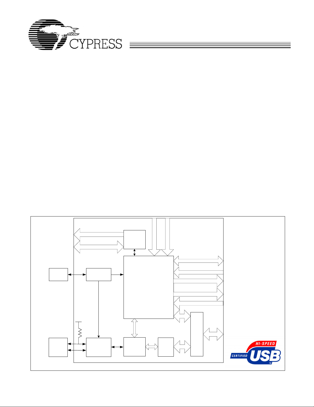
2.1 Block Diagram
2.0 Applications
• DSL modems
• AT A interface
• Memory card readers
• Legacy conversion devices
• Cameras
• Scanners
• Home PNA
• Wireless LAN
• MP3 players
•Networking
•Printers
The “Reference Designs” section of the Cypress web site
provides additional tools for typical USB applications. Each
reference design comes complete with firmware source code
and object code, schematic s, and documenta ti on. Please see
the Cypress web site at www.cypress. com .
24 MHz
XTAL
DPLUS
DMINUS
VCC
1.5K
USB 2.0 XCVR
SCL
SDA
PLL
I2C Bus
Controller
(Master On l y )
SX2 Internal Logic
CY Smart USB
FS/HS Engine
RESET#
WAKEUP*
4 KB
FIFO
Figure 2-1. Block Diagram
IFCLK*
Read*, Write*, OE*, PKTEND *, CS#
Interrupt#, Ready
Flags (3/4)
Address (3)
Control
FIFO
Data
8/16-Bit Data
Bus
Data
Cypress Semiconductor Corporation • 3901 North First Street • San Jose • CA 95134 • 408-943-2600
Document #: 38-08013 Rev. *E Revised July 13, 2004
1
FOR
FOR
CY7C6800
2.2 Introduction
The EZ-USB SX2™ USB interf ace device is designed to wo rk
with any external master, such as standard microprocessors,
DSPs, ASICs, and FPGAs to enable USB 2.0 support for any
peripheral design. SX2 has a built-in USB transceiver and
Serial Interface Engine (SIE), along with a command dec oder
for sending and receiving USB data. The controller has four
endpoints that share a 4-KB FIFO space for maximum flexibility and throughput, as well as Control Endpoint 0. SX2 has
three address pins and a selectable 8- or 16- bit data bus for
command and data input or out put.
2.3 System Diagram
Windows/USB Capable Host
USB Cable
USB Connection
Cypress
SX2
RAM/ROM
Device CPU Application
Figure 2-2. Example USB System Diagram
EEPROM
3.3 Boot Methods
During the power-up sequence, internal logic of the SX2
checks for the presence of an I
EEPROM, it will boot off the EEPROM. When the presence of
an EEPROM is detected, the SX2 checks the value of first
byte. If the first byte is found to be a 0xC4, the SX2 loads the
next two bytes into the IFCONFIG and POLAR registers,
respectively. If the fourth byte is also 0xC4, the SX2
enumerates using t he descriptor i n the EEPROM, then signal s
to the external master when enumeration is complete via an
ENUMOK interrupt (Section 3.4). If no EEPROM is detected,
the SX2 relies o n the extern al master f or the descr iptors. Once
this descriptor infor mation i s recei ve from the exte rnal mast er,
the SX2 will connect to the USB bus and enumerate.
3.3.1 EEPROM Organization
The valid sequence of bytes in the EEPROM are displayed
below
T able 3-1. Descriptor Lengt h Set to 0x06:
Default Enumeration
Byte Index Description
00xC4
1 IFCONFIG
2POLAR
30xC4
4 Descriptor Length (LSB):0x06
5 Descriptor Length (MSB): 0x00
6 VID (LSB)
7 VID (MSB)
8 PID (LSB)
9 PID (MSB)
10 DID (LSB)
1 1 DID (MSB)
2
C EEPROM.
[1,2]
If it finds an
3.0 Functional Overview
T able 3-2. Descriptor Length Not Set to 0x06
3.1 USB Signaling Speed
SX2 operates at two of the three rates def ined in the Universal
Serial Bus Specification Revision 2.0, dated April 27, 2000:
• Full-speed, with a signaling bit rate of 12 Mbits/s
• High-speed, with a signal ing bit rate of 480 Mbits/s.
SX2 does not support the low-speed signaling rate of 1.5
Mbits/s.
3.2 Buses
SX2 features:
• A selectable 8- or 16-bit bidirectional data bus
• An address bus for selecting the FIFO or Command Interface.
Notes:
1. Because there is no direct way to detect which EEPROM type (single or double address) is connected, SX2 uses the EEPROM address pins A2, A1, and A0
to determine whether to send out one or two bytes of address. Single-byte address EEPROMs (24LC01, etc.) should be strapped to address 000 and doublebyte EEPROMs (24LC64, etc.) should be strapped to address 001.
2. The SCL and SDA pins must be pulled up for this detection method to work properly, even if an EEPROM is not connected. Typical pull-up values are 2.2K – 10K
Ohms.
Document #: 38-08013 Rev. *E Page 2 of 42
Byte Index Description
00xC4
1IFCONFIG
2POLAR
30xC4
4 Descriptor Length (L SB)
5 Descriptor Length (MSB
6 Descriptor[0]
7 Descriptor[1]
8 Descriptor[2]

1
FOR
FOR
CY7C6800
• 0xC4: This initial byte tells the SX2 that this is a valid EEPROM with configuration information.
• IFCONFIG: The IFCONFIG byte contains the settings for
the IFCONFIG regi ster . The IFCONFI G register bi ts are defined in Section 7. 1. If the external master requires an interface configu ration different from the def ault, that interface
can be specified by this byte.
• POLAR: The Polar byte contains the polarity of the FIFO
flag pin signals. The POLAR register bits are defined in
Section 7.3. If th e external master requires signal polarity
differ ent from the default, the polari ty can be specified by
this byte.
• Descriptor: The Descriptor byte determines if the SX2
loads the desc riptor from the EEPROM. If this byt e = 0xC4,
the SX2 will l oad the descript or starting with the next byte.
If this byte does not equal 0xC4, the SX2 will wait for descriptor information from the external master.
• Descriptor Length: The Descriptor l ength is within the next
two bytes and i ndicate the length o f the descriptor con tained
within the EEPROM. The l ength is loaded least significant
byte (LSB) first, then most significant byte (MSB).
• Byte 7 Starts Descri ptor Inform ation: The descript or can
be a maximum of 500 bytes.
3.3.2 Default Enumeration
An optional d efault descr iptor can be used t o si mplif y enumeration. Onl y the V endor ID (VID), Product ID (PID), and Device
ID (DID) need t o b e loaded b y the SX2 f or i t to en umerate wi th
this default set-up. This information is either loaded from an
EEPROM in the case when the presence of an EEPROM
(Table 3-1) is detected, or the ext ernal master m ay simply l oad
a VID, PID, and DID when no EEPROM is present. In this
default enumeration, the SX2 uses the in-built default
descriptor (refer to Section 12.0).
If the descript or length loaded from the EEPROM is 6, SX2 will
load a VID, PID, and DID from the EEPROM and enumerate.
The VID, PID, and DID are loaded LSB, then MSB. For
example, if the VID, PID, and DID are 0x0547, 0x1002, and
0x0001, respectively, then the bytes should be stored as:
• 0x47, 0x05, 0x02, 0x10, 0x01, 0x00.
If there is no EEPROM, SX2 will wait for the external master
to provide the descriptor information. To use the default
descriptor, the external master must write to the appropriate
register (0x30) with descriptor length equal to 6 followed by the
VID, PID, and DID. Refer to Secti on 4.2 for fur ther info rmatio n
on how the external mast er may load the values.
The default descriptor enumerates four endpoints as listed in
the following page:
• Endpoint 2: Bulk out, 512 bytes in high-speed mode, 64
bytes in full-s peed m ode
• Endpoint 4: Bulk out, 512 bytes in high-speed mode, 64
bytes in full-s peed m ode
• Endpoint 6: Bulk in, 512 byt es in high-speed mode, 64 bytes
in full-speed mode
• Endpoint 8: Bulk in, 512 byt es in high-speed mode, 64 bytes
in full-speed mode.
The entire default descriptor is listed in Section 12.0 of this
data sheet.
3.4 Interrupt System
3.4.1 Architecture
The SX2 provides an output signal that indicates to the
external mast er t hat the SX2 has an inter rupt condi tion, or that
the data from a register re ad reques t is avail able. The SX2 has
six interrupt sources: SETUP, EP0BUF, FLAGS, ENUMOK,
BUSACTIVITY, and READY . Eac h interrup t can be enab led or
disabled by setting or clearing the corresponding bit in the
INTENABLE register.
When an interrupt occurs, the INT# pin will be asserted, and
the corresponding bit will be set in the Interrupt Status Byte.
The external master reads the Interrupt Status Byte by
strobing SLRD/SLOE. This presents the Interrupt Status Byte
on the lower portion of the data bus (FD[7:0]). Reading the
Interrupt Status Byte automatically clears the interrupt. Only
one interrupt request will occur at a time; the SX2 buffers
multiple pending interrupts.
If the ext ernal master has initiated a register read request, the
SX2 will buffer inte rrupts unt il the external master has read the
data. This insures that after a read sequence has begun, the
next interrupt that is received from the SX2 will indicate that
the corresponding data is available. Followi ng is a description
of this INTENABLE register.
3.4.2 INTENABLE Register Bit Definition
Bit 7: SETUP
If this interrupt is enabled, and the SX2 receives a set-up
packet from the USB host, the SX2 asserts the INT# pin and
sets bit 7 in the Int errupt St atus Byte. Th is inter rupt onl y occurs
if the set-up request is not one that the SX2 automatically
handles. For complete details on how to handle the SETUP
interr up t , re fe r to S ec ti o n 5 .0 of this data sheet .
Bit 6: EP0BUF
If this interrupt is enabl ed, and the Endpoi nt 0 buff er becomes
available to the external master for read or write operations,
the SX2 asserts the INT# pin and sets bit 6 in the Interrupt
Status Byte. This in terrupt i s used for handlin g the data ph ase
of a set-up req uest. Fo r comple te de tails on h ow to handle t he
EP0BUF interrupt, refer t o Secti on 5.0 of this data sheet.
Bit 5: FLAGS
If this int errupt is e nabled, and any O UT endpoi nt FIF O’ s stat e
changes from empty to not-empty, the SX2 asserts the INT#
pin and sets bit 5 in the Interrupt Status Byte. This is an
alternate way to monitor the status of OUT endpoint FIFOs
instead of using the FLAGA-FLAGD pins, and can be used to
indicate when an OUT packet has been received from the
host.
Bit 2: ENUMOK
If this interrupt is enabled and the SX2 receives a
SET_CONFIGURATION request from the USB host, the SX2
asserts the I NT# pin and sets bi t 2 i n the Int errup t Stat us Byte .
This event signals the completion of the SX2 enumeration
process.
Bit 1: BUSACTIVITY
If this interrupt is enabled, and the SX2 detects either an
absence or resumption of activity on the USB bus, the SX2
asserts the I NT# pin and sets bi t 1 i n the Int errup t Stat us Byte .
This usually indicates that the USB host is either suspending
Document #: 38-08013 Rev. *E Page 3 of 42

1
FOR
FOR
CY7C6800
or resuming or that a self-powered device has been plugged
in or unplugged. If the SX2 is bus-powered, the external
master must put the SX2 into a low-power mode after
detecting a USB suspend condition to be USB-compliant.
Bit 0: READY
If this interrupt is enabled, bit 0 in the Interrupt Status Byte is
set when the SX2 has powered up and performed a self-test.
The external master should always wait for this interrupt
before trying to read or write to the SX2, unless an external
EEPROM with a valid descriptor is present. If an external
EEPROM with a valid descriptor is present, the ENUMOK
interrupt will occur instead of the READY interrupt after power
up. A READY interrupt will also occur if the SX2 is awakened
from a low-power mode via the WAKEUP pin. This READY
interrupt i ndicates that the SX2 is ready for commands or data.
Although it is true that all interrupts will be buffered once a
command read request has been initiated, in very rare conditions, there might be a situation when there is a pending
interrupt already, when a read request is initiated by the
external master. In this case it is the interrupt status byte that
will be output when the external master asserts the SLRD. So,
a condition exists wher e the Int errup t Statu s Data Byt e can be
mistaken for t he resul t of a command re gister read requ est . In
order to get around this possible race condition, the first thing
that the external master must do on getting an interrupt from
the SX2 is check the status of the READY pin. If the READY
is low at the time the INT# was asserted, the data that will be
output when the external master strobes the SLRD is the
interrupt status byte (not the actual data requested). If the
READY pin is high at the time when the interrupt is asserted,
the data output on strobing the SLRD is the actual data byte
requested by the external master. So it is important that the
state of the READY pin be checked at the time the INT# is
asserted to ascertain the cause of the interrupt.
3.5 Resets and Wakeup
3.5.1 Reset
An input pi n (RESET#) reset s the chi p. The i nternal PLL s tabilizes af ter V
network (R = 100 K Ohms, C = 0.1 uf) is used to provide the
has reached 3.3V. Typically, an external RC
CC
RESET# signal. Th e Clock must be in a st able sta te for at l east
200 us before the RESET is released.
3.5.2 USB Reset When the SX2 detect s a USB Reset condi tion on the USB bus,
SX2 handles it like any other enumeration sequence. This
means that SX2 will enumerate again and assert the
ENUMOK interrupt to let the external master know that it has
enumerated. The external master will then be responsible for
configuring the SX2 for the application. The external master
should also check whether SX2 enumerated at High or Full
speed in order to adjust the EPxPKTLENH/L register values
accordingly. The last initialization task is for the external
master to flush all of the SX2 FIFOs .
3.5.3 Wakeup
The SX2 exits its low-power state when one of the following
events occur:
• USB bus signals a res um e. The SX2 will assert a BUSACTIVITY interrupt.
• The external master asserts the W AKEUP pin. The SX2 wi ll
assert a READY interrupt
[3]
.
3.6 Endpoint RAM
3.6.1 Size
• Control endpoint: 64 Bytes: 1 × 64 bytes (Endpoint 0).
• FIFO Endpoints: 409 6 Bytes: 8 × 51 2 by tes (E ndpoi nt 2, 4,
6, 8).
3.6.2 Organization
• EP0–Bidirectional Endpoint 0, 64-byte buff er.
• EP2, 4, 6, 8–Eight 512-byte buffers, bulk, interrupt, or isochronous. EP2 and EP6 can be either double-, triple-, or
quad-buffer ed. EP4 and EP8 c an only be do ubl e-buf fere d.
For high-speed endpoint configuration options, see
Figure 3-1.
Note:
3. if the descriptor loaded is set for remote wakeup enabled and the host does a set feature remote wakeup enabled, then the SX2 logic will perform RESUME
signalling after a WAKEUP interrupt.
Document #: 38-08013 Rev. *E Page 4 of 42
1
FOR
FOR
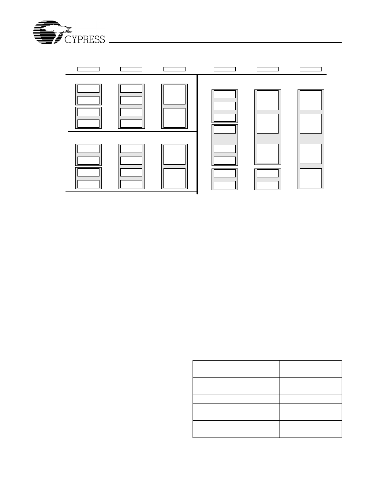
3.6.3 Endpoi nt Configurations (Hig h-speed Mode)
EP0 IN&OUT 64 64 64 64 64 64
CY7C6800
Group A
EP2
EP4
512
512
EP2
512
512
512
1024
512
EP2
512
1024
512
Group B
512
EP6
512
EP6
512
EP8
512
512
1024
512
EP6
512
1024
512
Figure 3-1. Endpoint Configuration
Endpoint 0 is the same for every configuration as it serves as
the CONTROL end point. For Endpoints 2, 4, 6, and 8, refer to
Figure 3-1. Endpoints 2, 4, 6, and 8 may be configured by
choosing eith er:
• One configuration from Group A and one from Group B
• One configuration from Group C.
Some example endpoi nt configurations are as foll ows.
• EP2: 1024 bytes double-buffered, EP6: 512 bytes quadbuffered.
• EP2: 512 bytes double-buffered, EP4: 512 bytes doublebuffered , EP6: 512 bytes doubl e-buf fere d, EP8: 512 bytes
double buffered.
• EP2: 1024 bytes quad-buf fered.
3.6.4 Default Endpoint Memory Configuration
At power-on-reset, the endpoint memories are configured as
follows:
• EP2: Bulk OUT, 512 bytes/packet, 2x buffered.
• EP4: Bulk OUT, 512 bytes/packet, 2x buffered.
• EP6: Bulk IN, 512 bytes/packet, 2x buffered.
• EP8: Bulk IN, 512 bytes/packet, 2x buffered.
3.7 External Interface
The SX2 presents two interfaces to the external master.
1. A FIFO interface thr ough which EP2, 4, 6, an d 8 data flows.
2. A command interf ace, which is used to set up the SX2, read
status, load descriptors, and access Endpoint 0.
Group C
EP2
EP6
EP8
512
512
512
EP2
512
512
512
512
EP8
512
1024
1024
1024
512
512
1024
1024
EP2
1024
1024
3.7.1 Architecture
The SX2 slave FIFO archit ecture has eight 512-byte blocks in
the endpoint RAM that directly serve as FIFO memories and
are controlled by FIFO control signals (IFCLK, CS#, SLRD,
SL WR, SLOE, PKTEND, and FIFOADR[2 :0]).
The SX2 command interface is used to set up the SX2, read
status, load descriptors, and access Endpoint 0. The
command interface has its own READY signal for gating
writes, and an INT# signa l to ind icate that the SX2 has data to
be read, or that an inter rupt event has occurred. The command
interface uses the same control signals (IFCLK, CS#, SLRD,
SLWR, SLOE, and FIFOADR[2:0]) as the FIFO interface,
except for PKTEND.
3.7.2 Control Signals
3.7.2.1 FIFOADDR Lines
The SX2 has three address pins that are used to select either
the FIFOs or the command interface. The addresses correspond to the following table.
Table 3-3. FIFO Address Lines Setting
Address/Selection FIFOADR2 FIFOADR1 FIFOADR0
FIFO2 0 0 0
FIFO4 0 0 1
FIFO6 0 1 0
FIFO8 0 1 1
COMMAND 1 0 0
RESERVED 1 0 1
RESERVED 1 1 0
RESERVED 1 1 1
Document #: 38-08013 Rev. *E Page 5 of 42

1
FOR
FOR
CY7C6800
The SX2 accepts either an internally derived clock (30 or 48
MHz) or externally supplied clock (IFCLK, 5-50 MHz), and
SLRD, SLWR, SLOE, PKTEND, CS#, FIFOADR[2:0] signals
from an external master. The interface can be selected for 8or 16- bit operation by an internal configuration bit, and an
Output Enable si gnal SLOE enabl es the dat a bus dr iver of th e
selected width. The external master must ensure that the
output enable signal is inactive when writing data to the SX2.
The interface can operate either asynchronously where the
SLRD and SLWR signals act directly as strobes, or synchronously where the SLRD and SL W R act as clock quali fiers. The
optional CS# sig nal wi ll trista te t he d ata bu s a nd ign ore SLRD,
SL W R, PKTEND.
The external master reads from OUT endpoints and writes to
IN endpoints, and reads from or writes to the command
interface.
3.7.2.2 Read: SLOE and SLRD
In synchronous mode, the FIFO pointer is incremented on
each rising edge of IFCLK while SLRD is asserted. In
asynchronous mo de, the FIFO pointer i s incremented on each
asserted-to-deasserted transit ion of SLRD.
SLOE is a d ata bus dr iver enable. When SLOE i s asserte d, the
data bus is driven by the SX2.
3.7.2.3 Write: SLWR
In synchronous mode, data on the FD bus is written to the
FIFO (and the FIFO pointer is incremented) on each rising
edge of IFCLK while SLWR is asserted. In asynchronous
mode, data on t he FD bus i s writ ten t o the F IFO (and th e FIFO
pointer is incremented) on each asserted-to-deasserted
transition of SLWR.
3.7.2.4 PKTEND
PKTEND commits the current buffer to USB. To send a short
IN packet (one which has not been filled to max packet size
determined by the value of PL[X:0] in EPxPKTLENH/L), the
external maste r st robes the PKTEND pin.
All these interface signals have a default polarity of low. In
order to change the polarity of PKTEND pin, the master may
write to the POLAR register anytime. In order to switch the
polarity of the SLWR/SLRD/SLOE, the master must set the
appropriate bit s 2, 3 and 4 respectively in th e FIFOPINPOLAR
register locat ed at XDATA space 0xE609. Please note that the
SX2 powers up with the polarities set to low. Section 7.3
provides further information on how to access this register
located at XDATA space.
3.7.3 IFCLK
The IFCLK pin can be c onfigured to be either an i nput (def ault)
or an output interface clock. Bits IFCONFIG[7:4] define the
behavior of the interface clock. To use the SX2’s intern allyderived 30- or 48-MHz clock, set IFCONFIG.7 to 1 and set
IFCONFIG.6 to 0 (30 MHz) or to 1 (48 MHz). T o use an externally supplied clock, set IFCONFIG.7=0 and drive the IFCLK
pin (5 MHz – 50 MHz). The input or output IFCLK signal can
be inverted by setting IFCONFIG.4=1.
3.7.4 FIFO Access
An external master can access the slave FIFOs either
asynchronously or synchronously :
• Asynchronous–SLRD, SLWR, and PKTEND pins are
strobes.
• Synchronous–SLRD, SLWR, and PKTEND pins are enables for the IFCLK clock pi n.
An external master accesses the FIFOs throu gh the data bus,
FD [15:0]. This bus can be either 8- or 16-bits wide; the width
is selected via the WORDWIDE bit in the EPxPKTLENH/L
registers. The data bus is bidirectional, with its output drivers
controlled by the SLOE pin. The FIFOADR[2:0] pins select
which of the four FIFOs is connected to the FD [15:0] bus, or
if the command interface is selected.
3.7.5 FIFO Flag Pins Configurat ion
The FIFO flags are FLAGA, FLAGB, FLAGC, and FLAGD.
These FLAGx pins report the status of the FIFO selected by
the FIFOADR[2:0] pins. At reset , the se pins are configured to
report the status of the following:
• FLAGA reports the stat us of the programmable flag.
• FLAGB reports the stat us of the full flag.
• FLAGC reports the status of the empty flag.
• FLAGD defaults to the CS# function.
The FIFO flags can either be indexed or fixed. Fixed flags
report the status of a particular FIFO regardless of the value
on the FIFOADR [2:0] pins. Indexed flags report the status of
the FIFO selected by the FIFOADR [2:0] pins.
[4]
3.7.6 Default FIFO Programmab le Fl ag Set- up
By default, FLAGA is the Programmable Flag (PF) for the
endpoint being pointed to by the FIFOADR[2:0] pins. For EP2
and EP4, the default endpoint configuration is BULK, OUT,
512, 2x, and the PF pin asserts when the entire FIFO has
greater than/equal to 512 b yte s. For EP6 a nd EP8, the defaul t
endpoint configuration is BULK, IN, 512, 2x, and the PF pin
asserts when t he entir e FIFO has less than /equal t o 512 by tes.
In other words, EP6/8 report a half-empty state, and EP2/4
report a half-full state. The polarity of the programmable flag
is set to active low and cannot be altered.
3.7.7 FIFO Programmable Flag (PF) Set-up
Each FIFO’s programmable-level flag (PF) asserts when the
FIFO reaches a user-defined fullness threshold. That
threshold is configured as follows:
1. For OUT packets: The thres hold i s sto red in PFC12 :0. Th e
PF is asserted when the number o f bytes i n the entire FI FO
is less than/equal to (DECIS = 0) or greater than/equal to
(DECIS = 1) the threshold.
2. For IN packets, with PKTSTAT = 1: The th reshol d is st ored
in PFC9:0. The PF is asserted when the number of bytes
written into the current packet in the FIFO i s less than/equa l
to (DECIS = 0) or greater than/equal to ( D ECIS = 1) the
threshold.
3. For IN packets, with PKTSTAT = 0: The th reshol d is st ored
in two parts: PKTS2:0 holds the numbe r of committed packets, and PFC9:0 holds the number of bytes in the current
packet. The PF is asserted when the FIFO is at or less full
than (DECIS = 0), or at or more full than (DE C IS = 1), the
threshold.
Document #: 38-08013 Rev. *E Page 6 of 42
1
FOR
FOR
CY7C6800
3.7.8 Command Protocol
An address of [1 0 0] on FIFOADR [2:0] will select the
command interface. The command interface is used to write
to and read from the SX2 registers and the Endpoint 0 buffer,
as well a s the des criptor RAM. Command read and write t ransactions occur over FD[7:0] only. Each byte written to the SX2
is either an address or a data byte, as determined by bit7. If
bit7 = 1, then the byte i s considered an address byte. If bit7 =
0, then the byte is considered a data byte. If bit7 = 1, then bit6
determines whether the address byte is a read request or a
write request. If bit6 = 1, then the byte is considered a read
request. If bit 6 = 0 then the byte is co nsider ed a write r equest.
Bits [5:0] hold the register address of the request. The format
of the command addre ss byte is shown in Table 3-4.
T able 3-4. Command Address Byte
Address/
Data#
Bit 7 Bit 6 Bit 5 Bit 4 Bit 3 Bit 2 Bit 1 Bit 0
Read/
Write# A5 A4 A3 A2 A1 A0
Each Write request is followed by two or more data bytes. If
another address byte is received before both data bytes are
received, t he SX2 ignores the first addr ess and any incompl ete
data transfers. The format for the data bytes is shown in
Table 3-5 and Table 3-6. Some registers take a series of byt es.
Each byte is transferred using the same protocol.
T able 3-5. Command Data Byte One
Bit 7 Bit 6 Bit 5 Bit 4 Bit 3 Bit 2 Bit 1 Bit 0
0 X X X D7 D6 D5 D4
T able 3-6. Command Data Byte T wo
Bit 7 Bit 6 Bit 5 Bit 4 Bit 3 Bit 2 Bit 1 Bit 0
0 X X X D3 D2 D1 D0
The first com mand data byt e contain s the upper nibble of data,
and the second command byte contains the lower nibble of
data.
3.7.8.1 Write Reques t Example
Prior to writing to a register, two conditions must be met:
FIFOADR[2:0] must hold [1 0 0], and the Ready line must be
HIGH. The external master should not initiate a command if
the READY pin is not in a HIgh state.
Example: to write the byte <10110000> into the IFCONFIG
register (0x01) , first send a command address byte as fol lows.
T able 3-7. Command Address Write Byte
Address/
Data#
Read/
Write# A5 A4 A3 A2 A1 A0
1 0000001
• The next six bits represent the register address (000001
binary = 0x01 hex).
Once the byte has been received the SX2 pulls the REA DY
pin low to inform the external master not to send any more
information. When the SX2 is ready to receive the next byte,
the SX2 pulls the READY pin high again. This next byte, the
upper nibble o f the d ata byt e, is writ ten to the SX2 as follows.
Table 3-8. Command Data Write Byte One
Address/
Data#
Don’t
Don’t
Care
0 XXX1011
Don’t
Care
Care D7 D6 D5 D4
• The first bit signifies that this is a data trans fer.
• The next three are don’t care bits.
• The next four bits hold th e upper nibble of the transferred
byte.
Once the byte has been received the SX2 pulls the REA DY
pin low to inform the external master not to send any more
information. When the SX2 is ready to receive the next byte,
the SX2 pulls the READY pin high again. This next byte, the
lower nibble of the data byte is written to the SX2.
Table 3-9. Command Data Write Byte Two
Address/
Data#
Don’t
Don’t
Care
0 XXX0000
Don’t
Care
Care D3 D2 D1 D0
At this point the entire byte <101 10000> has been transferred
to register 0x01 and the write sequence is complete.
3.7.8.2 Read Request Example
The Read cycle is simpler t han the write cycle. Th e Read cycl e
consists of a read reques t from the external master to t he SX2.
For example, to read the contents of register 0x01, a
command address byte is written to the SX2 as follows.
Table 3-10. Command Address Read Byte
Address/
Data#
Read/
Write# A5 A4 A3 A2 A1 A0
1 1000001
When the data is ready to be read, the SX2 asserts the INT#
pin to tell the external master that the data it requested is
waiting on FD[7:0].
[5]
• The first bit signifies an address transfer.
• The second bit signifie s that this is a write command.
Note:
4. In indexed mode, the value of the FLAGx pins is indeterminate except when addressing a FIFO (FIFOADR[2:0]={000,001,010,011}).
5. An important note: Once the SX2 receives a Read request, the SX2 allocates the interrupt line solely for the read request. If one of the six interrupt sources
described in Section 3.4 is asserted, the SX2 will buffer that interrupt until the read request completes.
Document #: 38-08013 Rev. *E Page 7 of 42

1
FOR
FOR
CY7C6800
4.0 Enumeration
The SX2 has two modes of enumeration. The first mode is
automatic through EEPROM boot load, as described in
Section 3.3. The second method is a manual load of the
descriptor or VID, PID, and DID as described below.
4.1 Standard Enumeratio n
The SX2 has 500 bytes of descriptor RAM into which the
external master may write its descriptor. The descriptor RAM
is accessed through register 0x30. To load a descriptor, the
external maste r does the following:
• Initiate a Write Request to register 0x30.
• Write two bytes (four command data transf ers) that define
the length of the entire descriptor about to be transferred.
The LSB is written first , fo llowed by the MSB.
• Write the descriptor, one byte at a time until complete.
Note: the register address is only written once .
After the entire descriptor has been transferred, the SX2 will
float the pull-up resistor connected to D+, and parse through
the descriptor to locate the individual descriptors. After the
SX2 has parsed the e ntir e desc ript or , the SX2 wi ll con nect th e
pull-up resistor and enumerate automatically. When enumeration is complete, the SX2 will notify the external master with
an ENUMOK interrupt.
The format and order of the descriptor should be as follows
(see Section 12.0 for an example):
• Device.
• Device qualifier.
• High-speed configuration, high-speed interface, highspeed endpoints.
• Full-speed configuration, full-speed interface, full-speed
endpoints.
• String.
4.2 Default Enumeration
The external master may si mply l oad a VI D, PID, and DID an d
use the defau lt des cript or bui lt i nto t he SX2. To use the default
descriptor, the descriptor length described above must equal
6. After the external master has written the length, the VID,
PID, and DID must be written LSB, t hen MSB. For example, if
the VID, PID, and DID are 0x04B4, 0x1002, and 0x0001
respectively, then the external master does the following:
• Initiates a Writ e Request to register 0x30.
• Writes two byte s (four command d ata transf ers) that define
the length of the entire descriptor about to be transferred.
In this case, the length is always six.
• Writes the V ID, PID, and DID bytes: 0xB4, 0x04, 0x02, 0x10,
0x01, 0x00 (in nibble format per the command protocol).
The default descriptor is listed in Section 12.0. The default
descriptor can be used as a starting point for a custom
descriptor.
Note:
6. These and all other data bytes must conform to the command protocol.
[6]
[6]
5.0 Endpoint 0
The SX2 wi ll automatica lly respon d to USB chapter 9 request s
without any external master intervention. If the SX2 receives
a request to which it cannot respond automatically, the SX2
will notify the external master. The external master then has
the choice of respond ing to the request or stalling.
After the SX2 receives a set-up packet to which it cannot
respond automatically, the SX2 will assert a SETUP interrupt.
After the external master reads the Interrupt Status Byte to
determine that the interrupt source was the SETUP interrupt,
it can initiate a read request to the SETUP register, 0x32.
When the SX2 sees a read request for the SETUP register, it
will present the first byte of set- up data to the external mast er.
Each additional read request will present the next byte of setup data, until all eight bytes have been read.
The external master can stall this request at this or any other
time. To stall a request, the external master initiates a write
request for the SETUP regi ster , 0x32, an d writes any non-zer o
value to the register.
If this set-up request has a data phase, the SX2 will then
interrupt the external master with an EP0BUF interrupt when
the buffer becomes available. The SX2 determines the
direction of the set -up request and interrupts when either:
• IN: the Endpoint 0 buff er becomes available to write to, or
• OUT : the Endpoint 0 buf fer r eceives a pac ket from the USB
host.
For an IN set-u p transaction, the external master can write up
to 64 bytes at a time for the data phase. The steps to write a
packet are as follows:
1. Wait for a n EP0BUF inte rrupt , indicat ing t hat the b uff er is
available.
2. Initiate a write request for register 0x31.
3. Write one data byte .
4. Repeat steps 2 and 3 until either all the data or 64 bytes
have been written, whichever is less.
5. Write the numbe r of byt es i n thi s packet to the b yt e count
register, 0x33.
T o se nd more than 64 byt es, the pr ocess is rep eated. The SX2
internally stores the length of the data phase that was
specified in the wLength field (bytes 6,7) of the set-up packet .
To send less than the requested amount of data, the external
master writes a packet that is less than 64 bytes, or if a multi ple
of 64, the external master follows the data with a zero-length
packet. When the SX2 sees a short or zero-length packet, it
will complete the set-up transfer by automatically completing
the handshake phase. The SX2 will not allow more data than
the wLength field specified in the set-up packet. Note: the
PKTEND pin does not apply to Endpoint 0. The only way to
send a short or zero length packet is by writing to the byte
count register with the appropriate value.
Document #: 38-08013 Rev. *E Page 8 of 42

1
FOR
FOR
CY7C6800
For an OUT set-up transaction, the external master can read
each packet received from the USB host during the data
phase. The steps to re ad a packet are as follows:
1. Wait f or an EP0BUF inte rrupt, indicati ng that a pac ket was
received from the US B host i nto the buffer.
2. Initiate a read re quest for the byte count regis ter, 0x33.
This indicates the amount of data received from the host.
3. Initiate a read re quest for register 0x31.
4. Read one byte.
5. Repeat steps 3 and 4 until the number of b ytes specified
in the byte count register has been read.
To receive more than 64 bytes, the process is repeated. The
SX2 internally stores the length of the data phase that was
specified in the wLength field of the set-up packet (bytes 6,7 ).
When the SX2 sees that the specified number of bytes have
been received, it will complete the set-up transfer by automatically comple ting the handshake phase. If the external master
does not wish to receive the entire transfer, it can stall the
transfer.
If the SX2 receives another set-up packet before the current
transfer has complet ed, it will int errupt the external master wi th
another SETUP in te rrupt. If the SX2 receives a set-up packet
with no data phase, the externa l master can accept the packet
and complete the handshak e pha se b y writ ing z ero t o the b yt e
count register.
The SX2 auto maticall y responds to all USB standard requests
covered in chapter 9 of the
USB 2.0 specification except the
Set/Clear F eature Endpoint r equests. When the host issues a
Set Feature or a Clear feature request, the SX2 will trigger a
SETUP interrupt to the external master. The USB spec
requires that the device respond to the Set endpoint feature
request by doing the fol lowing:
• Set the STALL condition on that endpoin t.
The USB spec requires that the device respond to the Clear
endpoint feature request by doing the following:
• Reset the Data Toggle for that endpoint
• Clear the STALL condition of that end point.
The register that is used to reset the data toggle TOGCTL
(located at XDATA location 0xE683) is not an index register
that can be addressed by the command protocol presented in
Section 3.7.8. The following section provides further information on this register bits and how to reset the data toggle
accordingly using a different set of command protocol
sequence.
5.1 Resetting Data Toggle
Following is the bi t def inition of the TOGCTL regis ter:
TOGCTL
Bit #
Bit Name Q S R I/O EP3 EP2 EP1 EP0
Read/Write R W W R/W R/W R/W R/W R/W
Default 00110010
7 6 5 4 3 2 1 0
Bit 7: Q, Data Toggle Value
Q=0 indicates DATA0 and Q=1 indicates DATA1, for the
endpoint sele cted by the I/O and EP3:0 bit s. Write the endpoi nt
select bits (IO and EP3: 0), before reading this value.
0xE683
Bit 6: S, Set Data Toggle to DATA1
After selecting the desired endpoint by writing the endpoint
select bits (IO and EP3:0), set S=1 to set the data toggle to
DATA1. The endpoint selection bits should not be changed
while thi s bit is wr itt e n.
Bit 5: R, Set Data Toggle to DATA0
Set R=1 to set the data toggle to DATA0. The endpoint
selection bits should not be changed while this bit is written.
Bit 4: IO , Select IN or OUT Endpoint
Set this bit to sel ect an endpoint direction prior to sett ing its R
or S bit. IO=0 selects an OUT endpoint, IO = 1 selects an IN
endpoint.
Bit 3-0: EP3:0, Select Endpoint
Set these bits to select an endpoint prior to setting its R or S
bit. Valid values are 0, 1, 2, , 6, and 8.
A two-step process is employed to clear an endpoint data
toggle bit to 0. First, write to the TOGCTL register with an
endpoint address (EP3 :EP0) plus a dire ction bit (IO ). Keeping
the endpoint and direction bits the same, write a “1” to the R
(reset) bit. For example, to clear the data toggle for EP6
configured as an “IN” endpoint, write the following values
sequentially to TOGCTL:
00010110b
00110110b
Following is the sequence of events that the master should
perform to set this register to 0x16:
(1) Send Low Byte of the Register (0x83)
• Command address write of address 0x3A
• Command data writ e of upper nibble of the Low Byte of
Register Address (0x08)
• Command data writ e of l ower nibble of the Low Byte of
Register Address (0x03)
(2) Send High Byte of the Register (0xE6)
• Command address write of address 0x3B
• Command data writ e of upper nibble of the High Byte of
Register Address (0x0E)
• Command data write of l ower nibble of the High Byte of
Register Address (0x06)
(3) Send the actual value to write to the register Register (in
this case 0x16)
• Command address write of address0x3C
• Command data writ e of upper nibble of the High Byte of
Register Address (0x01)
• Command data writ e of l ower nibble of the High Byte of
Register Address (0x06)
The same command sequence needs to be followed to set
TOGCTL register to 0x36. The same command protocol
sequence can be used to reset the data toggle for the other
endpoints. In order to read the status of this register, the
external master must do the following sequence of event s:
(1) Send Low Byte of the Register (0x83)
• Command address write of 0x3A
Document #: 38-08013 Rev. *E Page 9 of 42
1
FOR
FOR
• Command data write of upper nibble of the Low Byte of
Register Address (0x08)
• Command data write of lower nibble of the Low Byte of
Register Address (0x03)
(2) Send High Byte of the Register (0xE6)
• Command address writ e of address 0x3B
• Command data write of upper nibble of the High Byte of
Register Address (0x0E)
• Command data write of lowe r ni bble of the High Byte of
Register Address (0x06)
(3) Get the actual value from the TOGCTL regist er (0x16)
• Command address READ of 0x3C
6.0 Pin Assignments
6.1 56-pin SSOP
CY7C6800
1
FD13
2
FD14
3
FD15
4
GND
5
NC
6
VCC
7
GND
8
*SLRD
9
*SLWR
10
AVCC
11
XTALOUT
12
XTALIN
13
AGND
14
VCC
15
DPLUS
16
DMINUS
17
GND
18
VCC
19
GND
20
*IFCLK
21
RESERVED
22
SCL
23
SDA
24
VCC
25
FD0
26
FD1
27
FD2
28
FD3
*WAKEUP
*FLAGD/CS#
FIFOADR1
FIFOADR0
FIFOADR2
CY7C68001
56-pin SSOP
FD12
FD11
FD10
FD9
FD8
VCC
RESET#
GND
*PKTEND
*SLOE
INT#
READY
VCC
*FLAGC
*FLAGB
*FLAGA
GND
VCC
GND
FD7
FD6
FD5
FD4
56
55
54
53
52
51
50
49
48
47
46
45
44
43
42
41
40
39
38
37
36
35
34
33
32
31
30
29
Figure 6-1. CY7C68001 56-pin SSOP Pin Assignment
Note:
7. A * denotes programmable polarity.
Document #: 38-08013 Rev. *E Page 10 of 42
[7]

1
6.2 56-pin QFN
GND
56
VCC
55
FOR
FOR
CY7C6800
*
WAKEUP
FD15
FD14
FD13
FD12
FD11
NC
54
GND
53
52
51
50
49
FD10
484547
FD9
46
44
VCC
43
FD8
SLRD
*
SLW R
*
AVCC
XTAL O U T
XTAL IN
AGND
VCC
DPLUS
DMINUS
GND
VCC
GND
IFCLK
*
RESERVED
10
11
12
13
14
1
2
3
4
5
6
7
8
9
17
15
SCL
16
SDA
18
VCC
FD0
CY7C68001
56-pin Q FN
19
202721
FD1
FD2
FD3
22
FD4
23
FD5
24
FD6
25
FD7
26
GND
28
VCC
GND
42
41
40
39
38
37
36
35
34
33
32
31
30
29
RESET#
GND
FLAGD/CS#
*
PKTEND
*
FIFOAD R1
FIFOAD R0
FIFOAD R2
SLOE
*
INT#
READY
VCC
FLAGC
*
FLAGB
*
FLAGA
*
Figure 6-2. CY7C68001 56-pi n QF N Assignment
Document #: 38-08013 Rev. *E Page 11 of 42
[7]

1
FOR
FOR
CY7C6800
6.3 CY7C68001 Pin Definitions
T able 6-1. SX2 Pin Definitions
QFN
SSOP
Pin
Pin Name Type Default Description
3 10 AVCC Power N/A Analog V
6 13 AGND Power N/A Analog Ground. Connect to ground with as short a path as possible.
9 16 DMINUS I/O/Z Z USB D– Signal. Connect to the USB D– signal.
815DPLUSI/O/Z ZUSB D+ Signal. Connect to the USB D+ signal.
42 49 RESET# Input N/A Active LOW Reset. Rese ts the entire chip. This pin is normally tied to V
through a 100K resi stor, and to GND through a 0.1-µF capacitor.
5 12 XTALIN Input N/A Crystal Input. Connect this signal to a 24-MHz parallel-resonant, fundamental
mode crys tal and 20-pF capacitor to GND. It is also correct to drive XTALIN with
an external 24- MHz square wave derived from anothe r cl ock source.
4 11 XTALOUT Output N/A Crystal Output. Conn ect this signa l to a 24 -MHz parall el-reso nant , fun dament al
mode crystal and 20- pF capacitor to GND. If an external clock is used to drive
XTALIN, leave this pin open.
54 5 NC Output O No Connect. This pin must be left unconnected.
. This signal provi des power to the analog section of the chip.
CC
CC
33 40 READY Output L READY is an output-only ready that gates external command reads and writes.
Active High.
34 41 INT# Output H INT# is an output-only external interrupt signal. Active Low.
35 42 SLOE Input I SLOE is an input-onl y output enable with programmable polarity (POLAR.4) for
the slave FIFOs connected to FD[7:0] or FD[15:0].
36 43 FIFOADR2 Input I FIFOADR2 is an input-only address select for the slav e FIFOs connected to
FD[7:0] o r FD [ 1 5: 0 ].
37 44 FIFOADR0 Input I FIFOADR0 is an input-only address select for the slav e FIFOs connected to
FD[7:0] o r FD [ 1 5: 0 ].
38 45 FIFOADR1 Input I FIFOADR1 is an input-only address select for the slav e FIFOs connected to
FD[7:0] o r FD [ 1 5: 0 ].
39 46 PKTEND Input I PKTEND is an input-only packet end with programmable polari ty (POLAR.5) for
the slave FIFOs connected to FD[7:0] or FD[15:0].
40 47 FLAGD/CS#CS#:I
FLAGD:O
I FLAGD is a programmable slave- FIFO output status f lag signal. CS# is a mast er
chip select (default).
18 25 FD[0] I/O/Z I FD[0] is the bidirectional FIFO/Command data bus.
19 26 FD[1] I/O/Z I FD[1] is the bidirectional FIFO/Command data bus.
20 27 FD[2] I/O/Z I FD[2] is the bidirectional FIFO/Command data bus.
21 28 FD[3] I/O/Z I FD[3] is the bidirectional FIFO/Command data bus.
22 29 FD[4] I/O/Z I FD[4] is the bidirectional FIFO/Command data bus.
23 30 FD[5] I/O/Z I FD[5] is the bidirectional FIFO/Command data bus.
24 31 FD[6] I/O/Z I FD[6] is the bidirectional FIFO/Command data bus.
25 32 FD[7] I/O/Z I FD[7] is the bidirectional FIFO/Command data bus.
45 52 FD[8] I/O/Z I FD[8] is the bidirectional FIFO data bus.
46 53 FD[9] I/O/Z I FD[9] is the bidirectional FIFO data bus.
47 54 FD[10] I/O/Z I FD[10] is the bidir ectional FIFO data bus.
48 55 FD[11] I/O/Z I FD[11] is the bidirectional FIFO data bus.
49 56 FD[12] I/O/Z I FD[12] is the bidir ectional FIFO data bus.
50 1 FD[13] I/O/Z I FD[13] is the bidirectional FIFO data bus.
51 2 FD[14] I/O/Z I FD[14] is the bidirectional FIFO data bus.
52 3 FD[15] I/O/Z I FD[15] is the bidirectional FIFO data bus.
Document #: 38-08013 Rev. *E Page 12 of 42

1
FOR
FOR
CY7C6800
T able 6-1. SX2 Pin Definitions (continued)
QFN
SSOP
Pin
Pin Name Type Default Description
1 8 SLRD Input N/A SLRD is the input-only re ad strobe with programmable polari ty (POLAR.3) for the
slave FIFOs connected to FD[7:0] or FD[15:0].
2 9 SLWR Input N/A SLWR is the input-only write strobe with programmable polarity (POLAR.2) for
the slave FIFOs connected to FD[7:0] or FD[15:0].
29 36 FLAGA Output H FLAGA is a programmable slave-FIFO output status flag signal.
Defaults to PF for the FIFO se lected by th e FIFOADR [2:0] pins.
30 37 FLAGB Output H FLAGB is a programmable slave-FIFO output status flag signal.
Defaults to FULL for the FIFO selected by the FIFOADR[2:0] pins.
31 38 FLAGC Output H FLAGC is a programmable slave-FIFO output status flag signal.
Defaults to EMPTY for the FIFO selected by the FIFOADR[2:0] pins.
13 20 IFCLK I/O/Z Z Interface Clock, used for synchronously clocking data into or out of the slave
FIFOs. IFCLK al so serves as a tim ing referenc e for all slave FI FO control signals.
When using the internal clock reference (IFCONFIG.7=1) the IFCLK pin can be
configured to outp ut 30/48 MHz by setting bits IFCONFIG.5 and IFCONFIG.6.
IFCLK may be inver ted by se ttin g the bit IFCONFIG. 4=1. Pro grammable po lari ty.
14 21 Reserved Input N/A Reserved. Must be connected to ground.
44 51 WAKEUP Input N/A USB Wakeup. If th e SX2 is in suspend, asserting thi s pin starts up the oscill ator
15 22 SCL OD Z I
16 23 SDA OD Z I
and interrup ts t he SX2 to al low i t to exit the suspend mode. During normal
operation, ho lding W AKEUP asserted inhi bits the SX2 chip fro m suspending. This
pin has programmable polarity (POLAR.7).
2
C Clock. Connec t to V
EEPROM is attached.
2
C Data. Connect to V
is attached.
with a 2.2K-10 K Ohms resistor, even if no I2C
CC
with a 2. 2K-10 K Ohms res istor , even if no I2C EEPROM
CC
55 6 V
714 V
11 18 V
17 24 V
27 34 V
32 39 V
43 50 V
CC
CC
CC
CC
CC
CC
CC
Power N/A VCC. Connect to 3.3V power source.
Power N/A VCC. Connect to 3.3V power source.
Power N/A VCC. Connect to 3.3V power source.
Power N/A VCC. Connect to 3.3V power source.
Power N/A VCC. Connect to 3.3V power source.
Power N/A VCC. Connect to 3.3V power source.
Power N/A VCC. Connect to 3.3V power source.
53 4 GND Ground N/A Connect to ground.
56 7 GND Ground N/A Connect to ground.
10 17 GND Ground N/A Connect to ground.
12 19 GND Ground N/A Connect to ground.
26 33 GND Ground N/A Connect to ground.
28 35 GND Ground N/A Connect to ground.
41 48 GND Ground N/A Connect to ground.
Document #: 38-08013 Rev. *E Page 13 of 42

1
FOR
FOR
CY7C6800
7.0 Register Summary
T able 7-1. SX2 Register Summary
Hex Size Name Description D7 D6 D5 D4 D3 D2 D1 D0 Default Access
General Configuration
01 1 IFCONFIG Interface Configuration IFCLKSRC 3048MHZ IFCLKOE IFCLKPOL ASYNC STANDBY FLAGD/CS# DISCON 11001001 bbbbbbbb
02 1 FLAGSAB FIFO FLAGA and FLAGB Assign-
03 1 FLAGSCD FIFO FLAGC and FLAGD Assign04 1 POLAR FIFO polarities WUPOL 0 PKTEND SLOE SLRD SLWR EF FF 00000000 bbbrrrbb
05 1 REVID Chip Revision Major Major Major Major minor minor minor minor xxxxxxxx rrrrrrrr
Endpoint Configuration
06 1 EP2CFG Endpoint 2 Configuration VALID dir TYPE1 TYPE0 SIZE STALL BUF1 BUF0 10100010 bbbbbbbb
07 1 EP4CFG Endpoint 4 Configuration VALID dir TYPE1 TYPE0 0 STALL 0 0 10100000 bbbbrbrr
08 1 EP6CFG Endpoint 6 Configuration VALID dir TYPE1 TYPE0 SIZE STALL BUF1 BUF0 11100010 bbbbbbbb
09 1 EP8CFG Endpoint 8 Configuration VALID dir TYPE1 TYPE0 0 STALL 0 0 11100000 bbbbrbrr
0A 1 EP2PKTLENH E ndpoint 2 Packet Length H INFM1 OEP1 ZEROLEN WORD-
0B 1 EP2PKTLENL Endpoint 2 Packet Length L (IN only) PL7 PL6 PL5 PL4 PL3 PL2 PL1 PL0 00000000 bbbbbbbb
0C 1 EP4PKTLENH Endpoint 4 Packet Length H INFM1 OEP1 ZEROLEN WORD-
0D 1 EP4PKTLENL Endpoint 4 Packet Length L (IN only) PL7 PL6 PL5 PL4 PL3 PL2 PL1 PL0 00000000 bbbbbbbb
0E 1 EP6PKTLENH Endpoint 6 Packet Length H INFM1 OEP1 ZEROLEN WORD-
0F 1 EP6PKTLENL Endpoint 6 Packet Length L (IN only) PL7 PL6 PL5 PL4 PL3 PL2 PL1 PL0 00000000 bbbbbbbb
10 1 EP8PKTLENH Endpoint 8 Packet Length H INFM1 OEP1 ZEROLEN WORD-
11 1 EP8PKTLENL Endpoint 8 Packet Length L (IN only) PL7 PL6 PL5 PL4 PL3 PL2 PL1 PL0 00000000 bbbbbbbb
12 1 EP2PFH EP2 Programmable Flag H DECIS PKTSTAT IN: PKTS[2]
13 1 EP2PFL EP2 Programmable Flag L PFC7 PFC6 PFC5 PFC4 PFC3 PFC2 PFC1 PFC0 00000000 bbbbbbbb
14 1 EP4PFH EP4 Programmable Flag H DECIS PKTSTAT 0 IN: PKTS[1]
15 1 EP4PFL EP4 Programmable Flag L PFC7 PFC6 PFC5 PFC4 PFC3 PFC2 PFC1 PFC0 00000000 bbbbbbbb
16 1 EP6PFH EP6 Programmable Flag H DECIS PKTSTAT IN: PKTS[2]
17 1 EP6PFL EP6 Programmable Flag L PFC7 PFC6 PFC5 PFC4 PFC3 PFC2 PFC1 PFC0 00000000 bbbbbbbb
18 1 EP8PFH EP8 Programmable Flag H DECIS PKTSTAT 0 IN: PKTS[1]
19 1 EP8PFL EP8 Programmable Flag L PFC7 PFC6 PFC5 PFC4 PFC3 PFC2 PFC1 PFC0 00000000 bbbbbbbb
1A 1 EP2ISOINPKTS EP2 (if ISO) IN P ackets per frame (1-3) 0 0 0 0 0 0 INPPF1 INPPF0 00000001 bbbbbbb b
1B 1 EP4ISOINPKTS EP4 (if ISO) IN P ackets per frame (1-3) 0 0 0 0 0 0 INPPF1 INPPF0 00000001 bbbbbbb b
1C 1 EP6ISOINPKTS EP6 (if ISO) IN Packets per frame (1-3) 0 0 0 0 0 0 INPPF1 INPPF0 00000001 bbbbbbb b
1D 1 EP8ISOINPKTS EP8 (if ISO) IN Packets per frame (1-3) 0 0 0 0 0 0 INPPF1 INPPF0 00000001 bbbbbbb b
FLAGS
1E 1 EP24FLAGS Endpoints 2,4 FIFO Flags 0 EP4PF EP4EF EP4FF 0 EP2PF EP2EF EP2FF 00100010 rrrrrrrr
1F 1 EP68FLAGS Endpoints 6,8 FIFO Flags 0 EP8PF EP8EF EP8FF 0 EP6PF EP6EF EP6FF 01100110 rrrrrrrr
INPKTEND/FLUSH
20 1 INPK-
TEND/FLUSH
USB Configuration
2A 1 USBFRAMEH USB Frame count H 0 0 0 0 0 FC10 FC9 FC8 xxxxxxxx rrrrrrrr
2B 1 USBFRAMEL USB Frame count L FC7 FC6 FC5 FC4 FC3 FC2 FC1 FC0 xxxxxxxx rrrrrrrr
2C 1 MICROFRAME Microframe count, 0-7 0 0 0 0 0 MF2 MF1 MF0 xxxxxxxx rrrrrrrr
2D 1 FNADDR USB Function address HSGRANT FA6 FA5 FA4 FA3 FA2 FA1 FA0 00000000 rrrrrrrr
Interrupts
2E 1 INTENABLE Interrupt Enable SETUP EP0BUF FLAGS 1 1 ENUMOK BUSACTIVITY READY 11111111 bbbbbbbb
Descriptor
30 500 DESC Descriptor RAM d7 d6 d5 d4 d3 d2 d1 d0 xxxxxxxx wwwwww-
Endpoint 0
31 64 EP0BUF Endpoint 0 Buffer d7 d6 d5 d4 d3 d2 d1 d0 xxxxxxxx bbbbbbbb
32 8/1 SETUP Endpoint 0 Set-up Data / Stall d7 d6 d5 d4 d3 d2 d1 d0 xxxxxxxx bbbbbbbb
33 1 EP0BC Endpoint 0 Byte Count d7 d6 d5 d4 d3 d2 d1 d0 xxxxxxxx bbbbbbbb
Un-Indexed Register control
3A 1 Un-Indexed Register Low Byte pointer a7 a6 a5 a4 a3 a2 a1 a0
3B 1 Un-Indexed Register High Byte point-era7 a6 a5 a4 a3 a2 a1 a0
3C 1 Un-Indexed Register Data d7 d6 d5 d4 d3 d2 d1 d0
Address Un-I ndexed Registers in XDATA Space
0xE609 FIFOPINPOLAR FIFO Interface Pins Polarity 0 0 PKTEND SLOE SLRD SLWR EF FF 00000000 rrbbbbbb
0xE683 TOGCTL Data Toggle Control Q S R IO EP3 EP2 EP1 EP0 xxxxxxxx rbbbbbbb
ments
ments
[8]
[9]
Force Packet End / Flush FIFOs FIFO8 FIFO6 FIFO4 FIFO2 EP3 EP2 EP1 EP0 00000000 wwwwww-
Notes:
8. Please note that the SX2 was not designed to support dynamic modification of these endpoint configuration registers. If your applications need the ability to
change endpoint configurations after the device has already enumerated with a specific configuration, please expect some delay in being able to access the
FIFOs after changing the configuration. For example, after writing to EP2PKTLENH, you must wait for at least 35 us measured from the time the READY signal
is asserted before writing to the FIFO. This delay time varies for different registers and is not characterized, because the SX2 was not designed for this dynamic
change of endpoint configuration registers.
9. Please note that the SX2 was not designed to support dynamic modification of the INPKTEND/FLUSH register. If your applications need the ability to
endpoint configurations or access the INPKTEND register after the device has already enumerated with a specific configuration, please expect some delay in
being able to access the FIFOs after changing this register. After writing to INPKTEND/FLUSH, you must wait for at least 85 us measured from the time the
READY signal is asserted before writing to the FIFO. This delay time varies for different registers and is not characterized, because the SX2 was not designed
for this dynamic change of endpoint configuration registers
FLAGB3 FLAGB2 FLAGB1 FLAGB0 FLAGA3 FLAGA2 FLAGA1 FLAGA0 00000000 bbbbbbbb
FLAGD3 FLAGD2 FLAGD1 FLAGD0 FLAGC3 FLAGC2 FLAGC1 FLAGC0 00000000 bbbbbbbb
0 PL10 PL9 PL8 00110010 bbbbbbbb
0 0 PL9 PL8 00110010 bbbbbbbb
0 PL10 PL9 PL8 00110010 bbbbbbbb
0 0 PL9 PL8 00110010 bbbbbbbb
IN: PKTS[0]
OUT:PFC10
IN: PKTS[0]
OUT:PFC9
IN: PKTS[0]
OUT:PFC10
IN: PKTS[0]
OUT:PFC9
0 PFC9 PFC8 10001000 bbbbbbbb
0 0 PFC8 10001000 bbbbbbbb
0 PFC9 PFC8 00001000 bbbbbbbb
0 0 PFC8 00001000 bbbbbbbb
ww
ww
change
OUT:PFC12
OUT:PFC12
WIDE
WIDE
WIDE
WIDE
IN: PKTS[ 1]
OUT:PFC11
OUT:PFC10
IN: PKTS[ 1]
OUT:PFC11
OUT:PFC10
Document #: 38-08013 Rev. *E Page 14 of 42

1
7.1 IFCONFIG Register 0x01
FOR
FOR
CY7C6800
IFCONFIG
Bit #
Bit Name IFCLKSRC 3048MHZ IFCLKOE IFCLKPOL ASYNC STANDBY FLAGD/CS# DISCON
Read/Write R/W R/W R/W R/W R/W R/W R/W R/W
Default 11001001
7.1.1 Bit 7: IFCLKSRC
This bit selects the clock source for the FIFOs. If IFCLKSRC
= 0, the external clock on the IFCLK pin is selected. If
IFCL KSRC = 1 (def ault), an internal 30 or 48 MH z clock is
used.
7.1.2 Bit 6: 3048MHZ
This bit select s the int ernal FIFO clock frequenc y. If 3048MHZ
= 0, the internal clock frequency is 30 MHz. If 3048MHZ = 1
(default), the internal clock frequency is 48 MHz.
7.1.3 Bit 5: IFCLKOE
This bit selects if the IFCLK pin is driven. If IFCLKOE = 0
(default), t he IFCLK pi n is floated. If IFCLKOE = 1, the IFCLK
7 6 5 4 3 2 1 0
When ASYNC = 1 (default), the FIFOs operate asynchronously. No clock signal input to IFCLK is required, and the
FIFO control signals function directly as read and write
strobes.
7.1.6 Bit 2: ST ANDBY
This bit instructs the SX2 to enter a low-power mode. When
ST ANDBY=1, the SX2 will enter a low-power m ode by turning
off its oscillator. The external master shou ld wr it e this bit after
it receives a bus activity interrupt (indicating that the host has
signaled a USB suspend condition). If SX2 is disconnected
from the USB bus, the e xternal master can writ e this bit at any
time to save power. Once suspended, the SX2 is awakened
either by resumption of USB bus activity or by assertion of its
WAKEUP pin.
0x01
pin is driven.
7.1.7 Bit 1: FLAGD/CS#
7.1.4 Bit 4: IFCLKPOL
This bit control s the polarity of the IFCLK signal.
• When IFCLKPOL=0, the clock has the polari ty shown in all
This bit controls the function of the FLAGD/CS# pin. When
FLAGD/CS# = 0 (default), the pin operates as a slave chip
select. If FLAGD/CS# = 1, the pin oper ates as FLAGD.
the timing diagrams in this data sheet (rising edge is the
activating edge).
• When IFCLKPOL=1, the clock is inverted (in some cases
may help w ith sati s fying data set-up times).
7.1.5 Bit 3: ASYNC
This bit control s whether the FIFO int erface i s synchro nous or
asynchronous. When ASYNC = 0, the FIFOs ope rate synchr onously. In synchronous mode, a clock is supplied either internally or externally on the IFCLK pin, and the FIFO control
signals fu nction as read and write enable signal s for the clock
7.1.8 Bit 0: DISCON
This bit controls whether the internal pull-up resistor
connected to D+ is pu ll ed high or floating. Whe n DISCON = 1
(default), the pull-up resistor is floating simulating a USB
unplug. When DISCON=0, the pull-up resistor is pulled high
signaling a USB connection.
7.2 FLAGSA B/FLAG SCD Register s 0x02/0x03
The SX2 has four FIFO flags output pins: FLAGA, FLAGB,
FLAGC, FLAGD.
signal.
FLAGSAB
Bit #
Bit Name FLAGB3 FLAGB2 FLAGB1 FLAGB0 FLAGA3 FLAGA2 FLAGA1 FLAGA0
Read/Write R/W R/W R/W R/W R/W R/W R/W R/W
Default 00000000
7 6 5 4 3 2 1 0
0x02
FLAGSCD
Bit #
Bit Name FLAGD3 FLAGD2 FLAGD1 FLAGD0 FLAGC3 FLAGC2 FLAGC1 FLAGC0
Read/Write R/W R/W R/W R/W R/W R/W R/W R/W
Default 00000000
Document #: 38-08013 Rev. *E Page 15 of 42
7 6 5 4 3 2 1 0
0x03

1
FOR
FOR
CY7C6800
These flags can be programmed to represent various FIFO
flags using four select bits for each FIFO. The 4-bit codi ng for
all four flags is the same, as shown in the following table
.
T able 7-2. FIFO Flag 4-bit Coding
FLAGx3 FLAGx2 FLAGx1 FLAGx0 Pin Function
0 0 0 0 FLAGA = PF ,
FLAGB = FF,
FLAGC = EF,
FLAGD = CS#
(actual FIFO is
selected by
FIFOADR[2:0]
pins)
0001Reserved
0010Reserved
0011Reserved
0 1 0 0 EP2 PF
0 1 0 1 EP4 PF
0 1 1 0 EP6 PF
0 1 1 1 EP8 PF
1 0 0 0 EP2 EF
1 0 0 1 EP4 EF
1 0 1 0 EP6 EF
1 0 1 1 EP8 EF
1100EP2 FF
1101EP4 FF
1110EP6 FF
1111EP8 FF
For the default (0000) selection, the four FIFO flags are fixedfunction as shown in the first table entry; the input pins
FIFOADR[2:0] select to which of the four FIFOs the flags
correspond. These pins are decoded as shown in Table 3-3.
The other (non- zero) values of FLAGx[3:0] allow the designer
to independently configure the four flag outputs FLAGAFLAGD to correspond to any flag-Programmable, Full, or
Empty-from any of the four endpoint FIFOs. This allows each
flag to be assigned to any of the four FIFOs, including those
not currently selected by the FIFOADR [2:0] pins. For
example, the external master could be filling the EP2IN FIFO
with data while also checking the empty flag for the EP4OUT
FIFO.
7.3 POLAR Register 0x04
This register cont rols the polariti es of FIFO pin signals and the
WAKEUP pin.
POLAR
Bit #
Bit
Name
Read/W
rite
Default 0 0 0 0 0 000
7 6 5 4 3 2 1 0
WUPOL 0 PKTEND SLOE SLRD SLWR EF FF
R/W R/W R/W R R R R/W R/W
0x04
7.3.1 Bit 7: WUPOL
This flag sets the polarity of the WAKEUP pin. If WUPOL = 0
(default), t he polarity is acti ve LOW. If WUPOL=1, the polar it y
is active HIGH.
7.3.2 Bit 5: PKTEND
This flag selects the pol arit y of the PKTEND pin. If PKTEND =
0 (default), the polarity is active LOW. If PKTEND = 1, the
polarity is active HIGH.
7.3.3 Bit 4: SLOE
This flag selects the polarity of the SLOE pin. If SLOE = 0
(default), the polarity is active LOW. If SLOE = 1, the polarity
is active HIGH. This bit can only be changed by using the
EEPROM configuration load.
7.3.4 Bit 3: SLRD
This flag selects the polarity of the SLRD pin. If SLRD = 0
(default), the polarity is active LOW. If SLRD = 1, the polarity
is active HIGH. This bit can only be changed by using the
EEPROM configuration load.
7.3.5 S LWR Bit 2
This flag selects the polarity of the SLWR pin. If SLWR = 0
(default), the polarity is active LOW. If SLWR = 1, the polarity
is active HIGH. This bit can only be changed by using the
EEPROM configuration load.
7.3.6 EF Bit 1
This flag selects the polarity of the EF pin (FLAGA/B/C/D). If
EF = 0 (default), the EF pin is pulled low when the FIFO is
empty. If EF = 1, the EF pin is pulled HIGH when the FIFO is
empty.
7.3.7 FF Bit 0
This flag selects the polarity of the FF pin (FLAGA/B/C/D). If
FF = 0 (default), the FF pin is pulled low when the FIFO is full.
If FF = 1, the FF pin is pulled HIGH when the FIFO is full.
Note that bits 2(SLWR), 3(SLRD) and 4 (SLOE) are READ
only bits and cannot be set by the external master or the
EEPROM. On power-up, these bits are set to active low
polarity. In order to change the polarity after the device is
powered-up, the external master must access the previously
undocumented (un-indexed) SX2 register located at XDATA
space at 0xE609. This register has exact same bit definition
as the POLAR register except that bits 2, 3 and 4 defined as
SLWR, SLRD and SLOE respectively are Read/Write bits.
Following is the sequence of events that the master should
perform for s etting thi s register to 0x1C (set ting bi ts 4,3,and 2) :
1) Send Low Byte of the Register (0x09)
• Command address write of address 0x3A
• Command data write of upper nibble of the Low Byte of
Register Address (0x00)
• Command data write of lower nibble of the Low Byte of
Register Address (0x09)
Document #: 38-08013 Rev. *E Page 16 of 42

1
FOR
FOR
CY7C6800
(2) Send High Byte of the Register (0xE6)
• Command address write of address 0x3B
• Command data write of upper nibble of the High Byt e of
Register Address (0x0E)
• Command data write of lower nibble of th e High Byt e of
Register Address (0x06)
(3) Send the actual value to write to the register Register (in
this case 0x1C)
• Command address write of address 0x3C
• Command data write of upper nibble of the High Byt e of
Register Address (0x01)
• Command data write of lower nibble of th e High Byt e of
Register Address (0x0C)
In order t o avoid alter ing any other b its o f the F IFOPINPOLAR
register (0xE6 09) i nadver tentl y, the external m aster must do a
read (from POLAR register), modify the value to set/clear
appropriate bits and write the modified value to FIFOPINPOLAR register. The external master may read from the
POLAR register using the command read protocol as stated in
Section 3.7.8. Modify the value with the appropriate bit set to
change the polar ity as needed and wr i te this modi fied value t o
the FIFOPINPOLAR register.
7.4 REVID Register 0x05
These register bit s define the silicon revision.
REVID
Bit #
Bit
Name
Read/
Write
Default XXXXXXXX
7 6 5 4 3 2 1 0
Major Major Major Major Minor Minor Minor Minor
R/W R/W R/W R/W R/W R/W R/W R/W
0x05
The upper nibble is the maj or revision. The lower nibble is the
minor revision. For example: if REVID = 0x1 1, then the sili con
revision i s 1.1.
7.5 EPxCFG Register 0x06–0x09
These registers configure the large, data-handling SX2
endpoints, EP2, 4, 6, and 8. Figure 3-1 shows the configuration choices for these endpoints. Shaded blocks group
endpoint buffers for double-, triple-, or quad-buffering. The
endpoint direction is set independently—any shaded block
can have any direction.
EPxCFG
Bit #
Bit
Name
Read/
Write
Default 10100010
7 6 5 4 3 2 1 0
VALID DIR TYPE1 TYPE0 SIZE STALL BUF1 BUF0
R/W R/W R/W R/W R/W R/W R/W R/W
0x06, 0x08
.
EPxCFG
Bit #
Bit
Name
Read/W
rite
Default 10100010
7 6 5 4 3 2 1 0
VALID DIR TYPE1 TYPE0 SIZE STALL BUF1 BUF0
R/W R/W R/W R/W R R/W R R
0x07, 0x09
7.5.1 Bit 7: VALI D
The external master sets VALI D = 1 to activate an endpoint,
and VALID = 0 to deactivate it. All SX2 endpoints default to
valid. An endpoint whose VALID bit is 0 does not respond to
any USB traffic.
7.5.2 Bit 6: DIR
0 = OUT, 1 = IN. Defaults for EP2/4 a re DI R = 0, OUT, and fo r
EP6/8 are DIR = 1, IN.
7.5.3 Bit [5,4]: TYPE1, TYPE0
These bits define the endpoint type, as shown in Table 7-3.
The TYPE bits apply to all of the endpoint configuration
regist ers . A ll SX2 endpoints except EP0 default to BULK.
Table 7-3. Endpoint Type
TYPE1 TYPE0 Endpoint Type
00 Invalid
0 1 Isochronous
1 0 Bulk (Default)
1 1 Interrupt
7.5.4 Bit 3: SIZE
0 = 512 bytes (default), 1 = 1024 bytes.
Endpoints 4 and 8 can only be 512 bytes and is a read only
bit. The size of endpoin ts 2 and 6 is selectable.
7.5.5 Bit 2: STALL
Each bulk endpoint (IN or OUT) has a STALL bit (bit 2). If the
external master sets this bit, any requests to the endpoint
return a ST ALL handshake rather than ACK or NAK. The Get
Status-Endpoint Request returns the STALL state for the
endpoint indicated in byte 4 of the request. Note that bit 7 of
the endpoint number EP (byte 4) specifies directi on.
7.5.6 Bit [1,0]: BUF1, BUF0
For EP2 and EP6 the depth of endpoint buf fering is selected
via BUF1:0, as shown in Table 7-4. For EP4 and EP8 the
buffer is inter nally set to double buff ered and are read only bits .
Table 7-4. Endpoint Buffering
BUF1 BUF0 Buffering
00 Quad
01Invalid
[10]
1 0 Double
1 1 Triple
Notes:
10. Setting the endpoint buffering to invalid causes improper buffer allocation
Document #: 38-08013 Rev. *E Page 17 of 42

1
FOR
FOR
CY7C6800
7.6 EPxPKTLENH/L Registers 0x0A–0x11
The external master can use these registers to set smaller
packet sizes than the physical buffer size (refer to the previously de scrib ed EPxC FG regi st ers). T he defa ult packe t si ze is
512 bytes for all endpoints. Note that EP2 and EP6 can have
maximum sizes of 1024 bytes, and EP4 and EP8 can have
maximum sizes of 512 bytes, to be consistent with the
endpoint structure.
In addition, the EPxPKT LENH r egist er has four ot her e ndpoint
configuration bits.
EPxPKTLENL
Bit #
Bit Name PL7 PL6 PL5 PL4 PL3 PL2 PL1 PL0
Read/Write R/W R/W R/W R/W R/W R/W R/W R/W
Default 00000000
EP2PKTLENH,
EP6PKTLENH
Bit #
Bit Name INFM1 OEP1 ZERO
Read/Write R/W R/W R/W R/W R/W R/W R/W R/W
Default 0011 0010
EP4PKTLENH,
EP8PKTLENH
Bit #
Bit Name INFM1 OEP1 ZERO
Read/Write R/W R/W R/W R/W R/W R/W R/W R/W
Default 00110010
7 6 5 4 3 2 1 0
7 6 5 4 3 2 1 0
WORD
LEN
WIDE
7 6 5 4 3 2 1 0
WORD
LEN
WIDE
0 PL10 PL9 PL8
00 PL9PL8
7.6.1 Bit 7: INFM1 EPxPKTLENH.7
When the ext ernal mast er sets I NFM = 1 in an e ndpoint co nfiguration re gister, the FIFO flags for that endpoint become valid
one sample e arl ier than when the full condition occurs. These
bits take effect only when the FIFOs are operating synchronously according to an internally or externally supplied clock.
Having the FIFO flag indications one sample early simplifies
some synchronous interfaces. This applies only to IN
endpoints. Default is INFM1 = 0.
7.6.2 Bit 6: OEP1 EPxPKTLENH.6
When the external master sets an OEP = 1 in an endpoint
configuratio n register , t he FIFO flags for that endpoint become
valid one sample earlier than when the empty condition
occurs. These bits take effect only when the FIFOs are
operating synchronously according to an internally or externally supplied clock. Having the FIFO flag indications one
sample early simplifies some synchronous interfaces. This
applies only to OUT endpoints. Default is OEP1 = 0.
7.6.3 Bit 5: ZEROLEN EPxPKTLENH.5
When ZEROLEN = 1 (default), a zero length packet will be
sent when th e PKTEND pin i s asser ted an d t here ar e n o bytes
in the current packet. If ZEROLEN = 0, then a zero length
packet will not be sent under these conditions.
0x0B, 0x0D,
0x0F, 0x11
0x0A, 0x0E
0x0C, 0x10
7.6.4 Bit 4: WORDWIDE EPxPKTLENH.4
This bit controls whether the data interfa ce is 8 or 16 bits wide.
If WORDWIDE = 0, the data interface is eight bits wide, and
FD[15:8] have no function. If WORDWIDE = 1 (default), the
data interface is 16 bits wide.
7.6.5 Bit [2..0]: PL[X:0] Packet Length Bits
The default packet size is 512 bytes for all endpoints.
7.7 EPxPFH/L Register s 0x12–0x1 9
The Programmable Flag registers control when the PF goes
active for each of the four endpoint FIFOs: EP2, EP4, EP6,
and EP8. The EPxPFH/L fields are interpreted differently for
the high speed o peration and full speed operat ion and for OUT
and IN endpoints.
Following is the register bit definition f or high speed operation
and for full speed operation (when endpoint is configured as
an isochronous endpoi nt).
Full Speed ISO and High Speed Mode: EP2PFL,
EP4PFL, EP6PFL, EP8PFL
Bit #
Bit Name PFC7 PFC6 PFC5 PFC4 PFC3 PFC2 PFC1 PFC0
Read/Write R/W R/W R/W R/W R/W R/W R/W R/W
Default 00000000
Full Speed ISO and Hi gh Speed Mode:
EP4PFH, EP8PFH
Bit #
Bit Name DECIS PKTSTAT 0 IN:
Read/Write R/W R/W R/W R/W R/W R/W R/W R/W
Default 00001000
Full Speed ISO and High Speed Mode:
EP2PFH, EP6PFH
Bit #
Bit Name DECIS PKTSTAT IN:
Read/Write R/W R/W R/W R/W R/W R/W R/W R/W
Default 10001000
7 6 5 4 3 2 1 0
7 6 5 4 3 2 1 0
IN:
OUT:
IN:
PKTS[0]
OUT:
PFC9
IN:
PKTS[0]
OUT:
PFC10
PKTS[1]
OUT:
PFC10
7 6 5 4 3 2 1 0
PKTS[2]
PKTS[1]
OUT:
PFC12
PFC11
Following is the bit definition for the same register when the
device is operating at full speed and the endpoint is not
configured as isochronous endpoint.
Full Speed Non-ISO Mode: EP2PFL,
EP4PFL, EP6PFL, EP8PFL
Bit #
Bit Name IN:
Read/Write R/W R/W R/W R/W R/W R/W R/W R/W
Default 0 0 000000
7 6 5 4 3 2 1 0
IN:
PKTS[1]
OUT:
PFC7
PKTS[0]
PFC5 PFC4 PFC3 PFC2 PFC1 PFC0
OUT:
PFC6
0x13, 0x15,
0x17, 0x19
0x14, 0x18
0 0PFC8
0x12, 0x16
0 PFC9 PFC8
0x13, 0x15,
0x17, 0x19
Document #: 38-08013 Rev. *E Page 18 of 42

1
FOR
FOR
CY7C6800
Full Speed Non-ISO Mode:
EP2PFH, EP6PFH
Bit # 7 6 5 4 3 2 1 0
Bit Name DECIS PKTSTAT OUT:
Read/Write R/W R/W R/W R/W R/W R/W R/W R/W
Default 1 0 00100 0
Full Speed Non-ISO Mode:
EP4PFH, EP8PFH
Bit #
Bit Name DECIS PKT-
Read/Write R/W R/W R/W R/W R/W R/W R/W R/W
Default 0 0 0 0 1000
7 6 5 4 3 2 1 0
STAT
OUT:
PFC12
PFC11
0OUT:
PFC10
OUT:
PFC10
OUT:
PFC9
0x12, 0x16
0PFC9 IN:
PKTS[2]
OUT:
PFC8
0x14, 0x18
0 0PFC8
7.7.1 DECIS: EPxPFH.7
If DECIS = 0, t hen PF g oes hi gh whe n the b yte co unt i i s equal
to or less than what is defined in the PF registers. If DECIS =
1 (default), t hen PF goes high when the byte co unt equal to or
greater t han wh at i s set in th e PF regis ter. For OUT e ndpoi nts,
the byte count is the total number of b ytes i n the FIFO t hat ar e
available to the external master. For IN endpoints, the byte
count is determined by the PKSTAT bit.
7.7.2 PKSTAT: EPxPFH.6
For IN endpoints, the PF can apply to either the entire FIFO,
comprising multiple packets, or only to the current packet
being filled. If PKTST AT = 0 (def ault), the PF refers t o the entire
IN endpoint FIFO. If PKTST A T = 1, t he PF re fers to the number
of bytes in the current packet.
EPnPFH:L
PKTSTAT PF appli es to
0 Number of committed
format
PKTS[] and PFC[]
packe ts + cur rent packet
bytes
1 Curren t packet byt es only P F C[ ]
7.7.3 IN: PKTS(2:0)/ OUT: PFC[12:10]: EPxPFH[5:3]
These three bits have a different meaning, depending on
whether this is an IN or OUT endpoint.
7.7.3.1 IN Endpoints
If IN endpoint, the meaning of this EPxPFH[5:3] bits depend
on the PKTSTAT bit s etti ng. W hen PKTSTAT = 0 (def ault) , t he
PF considers wh en there ar e PKTS packets p lus PFC bytes in
the FIFO. PKTS[2:0] determines how many packets are
considered, according to the following table.
T able 7-5. PKTS Bits
PKTS2 PKTS1 PKTS0 Number of Packets
000 0
001 1
010 2
011 3
Table 7-5. PKTS Bits (continued)
PKTS2 PKTS1 PKTS0 Number of Packets
100 4
When PKTSTAT = 1, the PF consi ders when there are PFC
bytes in the FIFO, no matter how many packets are in the
FIFO. The PKTS[2:0] bits are ignored.
7.7.3.2 OUT Endpoints
The PF considers when there are PFC bytes in the FIFO
regardless of the PKTSTAT bit setting.
7.8 EPxISOINPKTS Registers 0x1A–0x1D
EP2ISOINOKTS, EP4ISOINPKTS,
EP6ISOINPKTS, EP8ISOINPKTS
Bit #
Bit Name 00000INPPF2INPPF1INPPF0
Read/Write R/W R/W R/W R/W R/W R/W R/W R/W
Default 00000 0 0 1
7 6 5 4 3 2 1 0
For ISOCHRONOUS IN endpoints only, these registers
determine the number of packets per frame (only one per
frame for full-speed mode) or microframe (up to three per
microframe for high-speed mode), according to the following
table.
Table 7-6. EPxISOINPKTS
INPPF1 INPPF0 Packets
0 0 Invalid
0 1 1 (default)
10 2
11 3
0x1A, 0x1B,
0x1C, 0x1D
7.9 EPxxFLAGS Registers 0x1E–0x1F
The EPxxFLAGS provide an alternate way of checking the
status of the endpoint FIFO flags. If enabled, the SX2 can
interrupt the external master when a flag is asserted, and the
external master can read t hese two registers to determ ine the
state of the FIFO fl ags. If the INF M1 and/ or OEP1 bit s are set ,
then the EPxEF and EPxFF bi ts are a ctually e mpty +1 and full
–1.
EP24FLAGS
Bit #
Bit Name 0 EP4PF EP4EF EP4FF 0 EP2PF EP4EF EP4FF
Read/Write R/W R/W R/W R/W R/W R/W R/W R/W
Default 00100010
EP68FLAGS
Bit #
Bit Name 0 EP8PF EP8EF EP8FF 0 EP6PF EP6EF EP6FF
Read/Write R/W R/W R/W R/W R/W R/W R/W R/W
Default 00100010
7 6 5 4 3 2 1 0
7 6 5 4 3 2 1 0
7.9.1 EPxPF Bit 6, Bit 2
This bit is the curr ent state of end poi nt x’ s programmabl e f lag.
0x1E
0x1F
Document #: 38-08013 Rev. *E Page 19 of 42

1
FOR
FOR
CY7C6800
7.9.2 EPxEF Bit 5, Bit 1
This bit is the current state of endpoint x’s empty flag. EPxEF
= 1 if the endpoint is empty.
7.9.3 EPxFF Bit 4, Bit 0
This bit is the current state of endpoint x’s f ull flag. EPxFF = 1
if the endpoint is full.
7.10 INPKT EN D /FLUS H Register 0x20
This register allows the external master to duplicate the
function of the PKTEND pin. The register also allows the
external master to selectively flush endpoint FIFO buffers.
INPKTEND/FLUSH
Bit #
Bit Name FIFO8 FIFO6 FIFO4 FIFO2 EP3 EP2 EP1 EP0
Read/Write WWWWWWWW
Default 0 0 0 00000
7 6 5 4 3 2 1 0
0x20
Bit [4..7 ]: FIF O x
These bits allows the external master to selectively flush any
or all of the endpoint FIFOs. By writing the desired endpoint
FIFO bit, SX2 logic flushes the selected FIFO. For example
setting bit 7 flushes endpoint 8 FIFO.
Bit [3..0]: EPx
These bits are is used only for IN transfers. By writing the
desired endpoint number (2,4,6 or 8), SX2 logic automatically
commits an IN buffer to the USB host. For example, for
committing a packet through endpoint 6, set the lower nibble
to 6: set bits 1 and 2 high.
7.11 USBFRAMEH/L Registers 0x2A, 0x2B
Every millisecond, the USB host sends an SOF token
indicating “Start Of Frame,” along with an 11-bit incrementing
frame count. The SX2 copies the frame count into these
registers at ever y SO F.
USBFRAMEH
Bit #
Bit Name 00000FC10FC9FC8
Read/Write RRRRRRRR
Default XXXXXXXx
USBFRAMEL
Bit #
Bit Name FC7 FC6 FC5 FC4 FC3 FC2 FC1 FC0
Read/Write RRRRRRRR
Default XXXXXXXX
7 6 5 4 3 2 1 0
7 6 5 4 3 2 1 0
One use of the frame count is to respond to the USB
SYNC_FRAME Request. If the SX2 detects a missing or
garbled SOF, the SX2 generates an internal SOF and increments USBFRAMEL–USBRAMEH.
0x2A
0x2B
7.12 MICROFRAME Registers 0x2C
MICROFRAME
Bit #
Bit Name 00000MF2MF1MF0
Read/Write RRRRRRRR
Default XXXXXXXx
7 6 5 4 3 2 1 0
MICROFRAME contains a count 0–7 that indicates which of
the 125 microsecond microframes last occurred.
This register is active only when SX2 is operating in highspeed mode (480 Mbits/sec).
0x2C
7.13 FNADDR Register 0x2D
During the USB enumera tion proce ss, the host sends a devi ce
a unique 7-bit address that the SX2 copies into this register.
There is normally no reason for the external master to know
its USB device address because the SX2 automatically
responds only to its assigned address.
FNADDR
Bit #
Bit Name HSGRANT FA6 FA5 FA4 FA3 FA2 FA1 FA0
Read/Write R RRRRRRR
Default 0 0000000
7 6 5 4 3 2 1 0
0x2D
Bit 7: HSGRANT, Set to 1 if the SX2 enumerated at high
speed. Set to 0 if the SX2 enumerated at full speed.
Bit[6..0]: Address set by the host.
7.14 INTENABLE Register 0x2E
This register is used to enable/disable the various interrupt
sources, and by defaul t all interrupts are enabled.
INTENABLE
Bit #
Bit Name SETUP EP0
Read/Write R/W R/W R/W R/W R/W R/W R/W R/W
Default 111111 1 1
7 6 5 4 3 2 1 0
FLAGS 1 1 ENUMOK BUS
BUF
ACTIVITY
7.14.1 SETUP Bit 7
Setting this bit to a 1 enables an inter rupt when a set-up packet
is received from the USB host.
7.14.2 EP0BUF Bit 6
Setting this bit to a 1 enables an interrupt when the Endpoint
0 buffer becomes available.
7.14.3 FLAGS Bit 5
Setting this bit to a 1 enables an interrupt when an OUT
endpoint FIFO’ s state transitions from em pty to not-empty.
7.14.4 ENUMOK Bit 2
Setting this bit to a 1 enables an interrupt when SX2 enumeration is co m ple te .
0x2E
READY
7.14.5 BUSACTIVITY Bit 1
Setting this bit to a 1 enables an interrupt when the SX2
detects an absence or pr esence of bus activity.
Document #: 38-08013 Rev. *E Page 20 of 42

1
FOR
FOR
CY7C6800
7.14.6 READY Bit 0
Setting this bit to a 1 enables an interrupt when the SX2 has
powered on and performed an internal self-test.
7.15 DESC Reg ister 0x30
This register address is used to write the 500-byte descriptor
RAM. The external master writes two bytes (four command
data transfers) to this address corresponding to the length of
the descrip tor or VID/PID/DID data to be written. The ext ernal
master then co nsecu tivel y wri tes th at num ber of b ytes i nto th e
descriptor RAM in nibble format. For complete details, refer to
Section 4.0.
7.16 E P0B UF Register 0x31
This register address is used to access the 64-byte Endpoint
0 buffer. The external master can read or write to this register
to complete Endpoint 0 data transfers. For complete details,
refer to Se c ti on 5. 0 .
7.17 SETUP Register 0x32
This register address is used to access the 8-byte set-up
packet received from the USB host. If the external master
writ es to thi s registe r, it ca n stall En dpoint 0. For com plete
details, refer to Sect ion 5.0.
7.18 EP0BC Register 0x33
This register address is used to access the byte count of
Endpoint 0. For Endpo int 0 OUT transfer s, the external master
can read this register to get the number of bytes transferred
from the USB host. For Endpoint 0 IN transfers, the external
master writes the number of bytes in the Endpoint 0 buffer to
transfer the bytes to the USB host . For complete det ail s, refer
to Section 5.0.
Document #: 38-08013 Rev. *E Page 21 of 42

1
FOR
FOR
CY7C6800
8.0 Absolute M aximum R atings
Storage Temperature .............. ........... .......................... ............................................... .........................................–65°C to +150°C
Ambient T emperature with Power Supplied............................................................................................... .. ... ....... .. ...0 ° C to +70 ° C
Supply Voltage to Ground Potential.........................................................................................................................–0.5V to +4.0V
DC Input Vol tage to Any Pin .......... .. .. ............... .. ............. .. .. ............................. ............... ..................................................... 5.25V
DC Voltage Applied to
Outputs i n Hig h -Z S ta te ...... .. .. ........ .. ............... .. ... ....... .. ............... .. ... ....... ... .. ....... ... ...................................... –0.5V to V
Power Dissipation .............................................................................................................................. .. ............ .. ............ ... 936 mW
Static Di s c harge Voltage.. ... .. ....... ... .............. ... .. ........ .. .. ........ .. ............... .. ... ....... .. ............... .................... ............... .......... > 2000V
9.0 Operating Conditions
TA (Ambi ent Tempera tu re U n der Bias) ......... ... .............. ... .. ........ .. .. ........ .. ............... .. ... ....... .. ...................... ... ............0°C to +70 ° C
Suppl y Voltage... .. .. ........ .. ... ....... .. ... ....... ... .............. ... .. ....... ... .. ....... ... .............. ... .. ........ .. .........................................+3.0V to +3.6V
Ground Voltage.......... ............ .. ........... ............ .. ............ .. ............................................................................................................ 0V
(Oscillator or Crystal Frequency ) .......................... ...................... ............ ...................... ................ ... ....... ... .............. . 24 MHz
F
OSC
± 100-ppm Parall el Resonant
+ 0.5V
CC
10.0 DC Electrical Characteristics
T able 10-1. DC Characteristics
Parameter Description Conditions
V
CC
V
IH
V
IL
I
I
V
OH
V
OL
I
OH
I
OL
C
IN
I
SUSP
I
SUSP
I
CC
T
RESET
Note:
11. Specific conditions for I
Supply Voltage 3.0 3.3 3.6 V
Input High Voltage 2 5.25 V
Input Low Voltage –0.5 0.8 V
Input Leakage Curr ent 0< VIN < V
Output Voltage High I
Output Voltage Low I
OUT
OUT
CC
= 4 mA 2.4 V
= –4 mA 0.4 V
Output Current High 4mA
Output Current Low 4mA
Input Pin Capacitance Except D+/D- 10 pF
D+/D- 15 pF
Suspend Current includes 1.5k integrated pull-up 250 400 µA
Suspend Current excluding 1.5k integrated pull-up 30 180 µA
Supply Current Connected to USB at high speed 200 260 mA
Connected to USB at full speed 90 150 mA
RESET Time after val id power Vcc min = 3.0V 1.91 mS
measurements: HS typical 3.3V, 25°C, 48 MHz; FS typical 3.3V, 25°C, 48 MHz.
CC
[11]
Min. Typ. Max. Unit
±10 µA
Document #: 38-08013 Rev. *E Page 22 of 42

1
FOR
t
FOR
11.0 AC Electrical Characteristics
11. 1 USB Transceiver
USB 2.0-certified compliant in full and high speed.
11.2 Command Interface
11.2.1 Command Synchronous Read
CY7C6800
IFCLK
IFCLK
SLRD
INT#
DATA
t
OEon
SLOE
Figure 11- 1. Comm and Synchronous Read Timing Diagram
t
SRD
t
RDH
t
INT
N
t
OEoff
[12]
T able 11-1. Command Synchronous Read Parameters with Internally Sourced IFCLK
Parameter Description Min. Max. Unit
t
IFCLK
t
SRD
t
RDH
t
OEon
t
OEoff
t
INT
T able 11-2. Command Synchronous Read with Externally Sourced IFCLK
IFCLK period 20.83 ns
SLRD to Clock Set-up Time 18.7 ns
Clock to SLRD Hold Time 0 ns
SLOE Turn-on to FIFO Data Valid 10.5 ns
SLOE Turn- off to FI F O Dat a H o ld 10.5 n s
Clock to INT# Output Propagat ion Delay 9.5 ns
[13]
Parameter Description Min. Max. Unit
t
IFCLK
t
SRD
t
RDH
t
OEon
t
OEoff
t
INT
Notes:
12. Dashed lines denote signals with programmable polarity.
13. Externally sourced IFCLK must not exceed 50 MHz.
IFCLK Period 20 200 ns
SLRD to Clock Set-up Time 12.7 ns
Clock to SLRD Hold Time 3.7 ns
SLOE Turn-on to FIFO Data Val id 10.5 ns
SLOE Turn-off to FIFO Data Hold 10.5 ns
Clock to INT# Output Propagation Delay 13.5 ns
Document #: 38-08013 Rev. *E Page 23 of 42

1
FOR
t
FOR
11.2.2 Command Synchronous Write
IFCLK
CY7C6800
IFCLK
t
SLWR
DATA
READY
SWR
Figure 11- 2. Comm and Synchronous Write Timing Diagram
t
SFD
t
WRH
t
FDH
N
t
NRDY
t
NRDY
[12]
Table 11-3. Command Synchronous Write Parameters with Internally Sourced IFCLK
Parameter Description Min. Max. Unit
t
IFCLK
t
SWR
t
WRH
t
SFD
t
FDH
t
NRDY
T able 11-4. Command Synchronous Write Parameters with Externally Sourced IFCLK
IFCLK Period 20.83 ns
SLWR to Clock Set-up Time 18.1 ns
Clock to SLWR Hold Time 0 ns
Command Data to Clock Set-up Time 9.2 ns
Clock to Command Data Hold Time 0 ns
Clock to READY Output Propagation Time 9.5 ns
[13]
Parameter Description Min. Max. Unit
t
IFCLK
t
SWR
t
WRH
t
SFD
t
FDH
t
NRDY
IFCLK Period 20 200 ns
SLWR to Clock Set-up Time 12.1 ns
Clock to SLWR Hold Time 3.6 ns
Command Data to Clock Set-up Time 3.2 ns
Clock to Command Data Hold Time 4.5 ns
Clock to READY Output Propagation Time 13.5 ns
Document #: 38-08013 Rev. *E Page 24 of 42

1
FOR
t
FOR
11.2.3 Command Asynchronous Read
CY7C6800
RDpwh
SLRD
t
INT#
DATA
SLOE
IRD
t
OEon
Figure 11- 3. Command Asynchronous Read Timing Diagram
t
RDpwl
t
XINT
N
t
OEoff
[12]
T able 11-5. Command Read Parameters
Parameter Description Min. Max. Unit
t
RDpwl
t
RDpwh
t
IRD
t
XINT
t
OEon
t
OEoff
SLRD Pulse Width LOW 50 ns
SLRD Pulse Width HIGH 50 ns
INTERR UPT to SLRD 0 ns
SLRD to INTERRUPT 70 ns
SLOE Turn-on to FIFO Data Valid 10.5 ns
SLOE Turn- off to FI F O Dat a H o ld 10.5 n s
11.2.4 Command Asynchronous Write
t
FDH
t
WRpwh
SLWR
DATA
t
WRpwl
t
SFD
READY
t
RDYWR
Figure 11-4. Command Asynchronous Write Timing Diagram
t
RDY
t
NRDY
[12]
T able 11-6. Command Write Parameters
Parameter Description Min. Max. Unit
t
WRpwl
t
WRpwh
t
SFD
t
FDH
t
RDYWR
t
RDY
SL W R Pulse LOW 50 ns
SL W R Pulse HI GH 70 ns
SL W R to Command DATA Set-up Time 10 ns
Command DATA to SLWR Hold Time 10 ns
READY to SLWR Time 0 ns
SL W R to READY 70 ns
Document #: 38-08013 Rev. *E Page 25 of 42

1
FOR
t
FOR
11.3 FIFO Interface
11.3.1 Slave FIFO Synchronous Read
CY7C6800
IFCLK
IFCLK
SLRD
FLAGS
DATA
SLOE
t
OEon
N
Figure 11- 5. Sl ave FIFO Synchronous Read Timing Diagram
T able 11-7. Slave FIFO Synchronous Read with Internally Sourced IFCLK
t
SRD
t
RDH
t
XFLG
t
XFD
N+1
[13]
t
OEoff
[12]
Parameter Description Min. Max. Unit
t
IFCLK
t
SRD
t
RDH
t
OEon
t
OEoff
t
XFLG
t
XFD
Table 11-8. Slave FIFO Synchronous Read with Externally Sourced IFCLK
IFCLK Period 20.83 ns
SLRD to Clock Set-up Time 18.7 ns
Clock to SLRD Hold Time 0 ns
SLOE Turn-on to FIFO Data Valid 10.5 ns
SLOE Turn- off to FI F O Dat a H o ld 10.5 n s
Clock to FLAGS Output Propagati on Delay 9.5 ns
Clock to FIFO Data Output Propagation Delay 11 ns
[13]
Parameter Description Min. Max. Unit
t
IFCLK
t
SRD
t
RDH
t
OEon
t
OEoff
t
XFLG
t
XFD
IFCLK Period 20 200 ns
SLRD to Clock Set-up Time 12.7 ns
Clock to SLRD Hold Time 3.7 ns
SLOE Turn-on to FIFO Data Val id 10.5 ns
SLOE Turn-off to FIFO Data Hold 10.5 ns
Clock to FLAGS Output Propagation Delay 13.5 ns
Clock to FIFO Data Output Prop agation Delay 15 ns
Document #: 38-08013 Rev. *E Page 26 of 42

1
FOR
FOR
11.3.2 Slave FIFO Synchronous Write
IFCLK
t
IFCLK
CY7C6800
SLWR
DATA
FLAGS
Figure 11-6. Slave FIFO Synchronous Writ e Timing Diagram
T able 11-9. Slave FIFO Synchronous Write Parameters with Inter nally Sourced IFCLK
t
SWR
t
WRH
N
t
SFDtFDH
t
XFLG
[12]
[13]
Parameter Description Min. Max. Unit
t
IFCLK
t
SWR
t
WRH
t
SFD
t
FDH
t
XFLG
T able 11-10. Slave FIFO Synchronous Write Parameters with Extern all y Sourced IFCLK
IFCLK Period 20.83 ns
SLWR to Clock Set-up Time 18.1 ns
Clock to SLWR Hold Time 0 ns
FIFO Data to Clock Set-up Time 9.2 ns
Clock to FIFO Data Hold Ti m e 0 ns
Clock to FLAGS Output Propagati on Time 9.5 ns
[13]
Parameter Description Min. Max. Unit
t
IFCLK
t
SWR
t
WRH
t
SFD
t
FDH
t
XFLG
IFCLK Period 20 ns
SLWR to Clock Set-up Time 12.1 ns
Clock to SLWR Hold Time 3.6 ns
FIFO Data to Clock Set-up Time 3.2 ns
Clock to FIFO Data Hold Ti m e 4 .5 ns
Clock to FLAGS Output Propagati on Time 13.5 ns
Document #: 38-08013 Rev. *E Page 27 of 42

1
FOR
FOR
11.3.3 Slave FIFO Synchronous Packet End Strobe
IFCLK
PKTEND
FLAGS
Figure 11-7. Slave FIFO Synchronous Packet End Strobe Timing Diagram
t
SPE
t
PEH
t
XFLG
CY7C6800
[12]
T able 11-11. Slave FIFO Synchronous Packet End Str obe Parameters, Internally Sourced IFCLK
[13]
Parameter Description Min. Max. Unit
t
IFCLK
t
SPE
t
PEH
t
XFLG
T able 11-12. Slave FIFO Synchronous Packet End Strobe Parameters, Externally Sourced IFCLK
IFCLK Period 20.83 ns
PKTEND to Clock Set-up Time 14.6 ns
Clock to PKTEND Hold Time 0 ns
Clock to FLAGS Output Propagati on Delay 9.5 ns
[13]
Parameter Description Min. Max. Unit
t
IFCLK
t
SPE
t
PEH
t
XFLG
IFCLK Period 20 200 ns
PKTEND to Clock Set-up Time 8.6 ns
Clock to PKTEND Hold Time 2.5 ns
Clock to FLAGS Output Propagati on Delay 13.5 ns
11.3.4 Slave FIFO Synchronous Address
IFCLK
SLCS#/FIFOADR[2:0]
t
SFAtFAH
Figure 11-8. Slave FIFO Synchronous Address Timing Diagram
T able 11-13. Slave FIFO Synchronous Address Parameters
[13]
Parameter Description Min. Max. Unit
t
IFCLK
t
SFA
t
FAH
Document #: 38-08013 Rev. *E Page 28 of 42
Interface Clock Peri od 20 200 ns
FIFOADR[2:0] to Clock Set-up Time 25 ns
Clock to FIFOADR[2:0] Hold Time 10 ns

1
FOR
FOR
11.3.5 Slave FIFO Asynchronous Read
t
RDpwh
CY7C6800
SLRD
FLAGS
DATA
SLOE
t
OEon
N
Figure 11-9. Slave FIFO Asynchronous Read Timi ng Diagram
T able 11-14. Slave FIFO Asynchronous Read Parameters
t
RDpwl
t
XFD
[14]
N+1
t
XFLG
t
OEoff
[12]
Parameter Description Min. Max. Unit
t
RDpwl
t
RDpwh
t
XFLG
t
XFD
t
OEon
t
OEoff
SLRD Pulse Width Low 50 ns
SLRD Pulse Width HIGH 50 ns
SLRD to FLAGS Output Propagation Delay 70 ns
SLRD to FIFO Data Output Propagation Dela y 15 ns
SLOE Turn-on to FIFO Data Valid 10.5 ns
SLOE Turn- off to FI F O Dat a H o ld 10.5 n s
11.3.6 Slave FIFO Asynchronous Write
t
WRpwh
SLWR/SLCS#
t
WRpwl
t
SFD
t
FDH
DATA
t
FLAGS
Figure 11-10. Slave FIFO Asynchronous Wri te Timing Diagram
T able 11-15. Slave FIFO Asynchronous Write Parameter s with Internally Sourced IFCLK
XFD
[12]
[14]
Parameter Description Min. Max. Unit
t
WRpwl
t
WRpwh
t
SFD
t
FDH
t
XFD
Note:
14. Slave FIFO asynchronous parameter values are using internal IFCLK setting at 48 MHz.
SL W R Pulse LOW 50 ns
SL W R Pulse HI GH 70 ns
SLWR to FIFO DATA Set-up Time 10 ns
FIFO DATA to SLWR Hold Time 10 ns
SLWR to FLAGS Output Propagation Delay 70 ns
Document #: 38-08013 Rev. *E Page 29 of 42

1
FOR
FOR
11.3.7 Slave FIFO Asynchronous Packet End Strob e
PKTEND
FLAGS
Figure 11-11. Sla ve FIFO Asynchronous Packet End Strobe Timing Diagram
t
PEpwl
t
XFLG
t
PEpwh
CY7C6800
T able 11-16. Slave FIFO Asynchronous Packet End Strobe Parameters
[14]
Parameter Description Min. Max. Unit
t
PEpwl
t
PWpwh
t
XFLG
PKTEND Pulse Width LOW 50 ns
PKTEND Pulse Width HIGH 50 ns
PKTEND to FLAGS Output Propagation Delay 110 ns
11.3.8 Slave FIFO Asynchronous Address
SLCS/FIFOADR[2:0]
t
t
SLRD/SLWR/PKTEND
SFA
Figure 11-12. Slave FIFO Asynchronous Address Ti m ing Dia gram
T able 11-17. Slave FIFO Asynchronous Address Parameters
[14]
FAH
[12]
Parameter Description Min. Max. Unit
t
SFA
t
FAH
t
FAH
11.4 Slave FIFO Address to Flags/Data
FIFOADR[2:0] to RD/WR/PKTEND Set-up Time 10 ns
SLRD/PKTEND to FIFOADR[2:0] Hold Time 20 ns
SL W R to FIFOADR[ 2:0] Hold Time 70 ns
Following timing is applicable to synchronous and asynchronous int erfaces.
FIFOADR [2.0]
t
XFLG
FLAGS
t
XFD
DATA
Figure 11-13. Slave FIFO Address to Flags/Data Timing Diagram
NN+1
[11]
T able 11-18. Slave FIFO Address to Flags/Data Parameters
Parameter Description Min. Max. Unit
t
XFLG
t
XFD
Document #: 38-08013 Rev. *E Page 30 of 42
FIFOADR[2:0] to FLAGS Output Propagation Delay 10.7 ns
FIFOADR[2:0] to FIFODATA Output Propagation Delay 14.3 ns

1
FOR
FOR
11.5 S lave FIFO Outp ut Enable
Following timings are applicable to synchronous and asynchronous interfaces.
SLOE
t
DATA
t
OEon
OEoff
CY7C6800
Figure 11-14. Slave FIFO Output Enable Timing Di agram
[11]
T able 11-19. Slave FIFO Output Enable Parameters
Parameter Description Min. Max. Unit
t
OEon
t
OEoff
SLOE assert to FIFO DATA Output 10.5 ns
SLOE deassert to FIFO DATA Hold 10.5 ns
11.6 Sequ ence Diagr am
1 1.6.1 Single and Burst Synchronous Read Example
t
IFCLK
IFCLK
t
T=0
SFA
T=2
>= t
SRD
>= t
RDH
FIFOADR
SLRD
SLCS
FLAGS
t
SFA
t=0
t
SRD
t=2
t
FAH
t
RDH
t=3
t
XFLG
T=3
t
FAH
DATA
Data Driven: N
t
OEon
N+1
t
XFD
N+2
t
XFD
t
XFD
N+1
t
t
OEoff
OEon
N+3
t
XFD
N+4
t
OEoff
SLOE
t=1
t=4
T=1
T=4
Figure 11-15. Slave FIFO Synchronous Read Sequence and Timing Diagram
FIFO POINTER
FIFO DATA BUS
IFCLK
NNN+1 N+2
SLOE
Not Driven Driven: N
IFCLK IFCLK IFCLK IFCLK
SLRD
SLOE
SLRD
N+1 N+2 N+3 Not Driven
N+1
Not Driven
SLOE
N+1
SLRD
N+1
N+3
IFCLK
N+4
N+4
SLRD
IFCLK IFCLKIFCLK IFCLK
N+4
N+4
N+4
SLOE
Figure 11-16. Slave FIFO Synchronous Sequence of Events Diagram
Document #: 38-08013 Rev. *E Page 31 of 42

1
FOR
FOR
CY7C6800
Figure 11-15 shows th e t iming rel ations hip o f th e SL A VE FI FO
signals during a synchronous FIFO read using IFCLK as the
synchronizing clock. The diagram illustrates a single read
followed by a burst read.
• At t = 0 the FIFO addr ess is stable and the signal SLCS is
asserted (SLCS may be tied low in some applications).
Note: t
IFCLK is running at 48 MHz, the FIFO address setup time
has a minimum of 25 nsec. This means when
SFA
is more than one IFCLK cycle.
• At = 1, SLOE is asserted. SLOE is an output enable only,
whose sole function is to dri ve the data bus. The dat a that
is driven on the bus is the data that the interna l FIFO pointer
is currently pointing to. In this example it is the first data
value in the FIFO. Not e: the data is pre-fetche d and is driven
on the bus when SLOE is asserted .
• At t = 2, SLRD is asserte d. SLRD must meet the set up time
of t
(time from asserting the SLRD signal to the rising
SRD
edge of the IFCLK) and maintai n a minimum hold time of
t
(time from the IFCLK edge to the deassertion of the
RDH
SLRD signal). I f the SLCS signal is u sed, it must be as serted
with SLRD, or before SLRD is ass erted ( i.e. the SLCS and
t
IFCLK
IFCLK
t
FIFOADR
SLWR
SFA
t=0
t
SWR
t=2
t=3
t
WRH
t
FAH
T=0
SLRD signals must both be asserted to start a valid read
condition).
• The FIFO pointer is up dated on the rising e dge of the IFCLK,
while SLRD is asserte d. This st arts the propaga tion of dat a
from the newly ad dressed location to t he data bus. After a
propagation delay of t
of IFCLK) the ne w data value is present. N is the fir st data
(measured from the rising edge
XFD
value read from t he FIFO. In order to have data on the FIFO
data bus, SLOE MUST also be asserted.
The same sequence of events are shown for a burst read and
are marked with the time indicators of T = 0 through 5. Note:
For the burst mode, the SLRD and SLOE are left asserted
during the entire dur ation of the read. In the burst read mode,
when SLOE is asserted, data indexed by the FIFO pointer is
on the data bus. During t he first read cycle, on the rising edge
of the clock the FIFO pointer is updated and increments to
point to address N+1. For each subsequent rising edge of
IFCLK, while the SLRD is asserted, the FIFO pointer is incremented and the next data value is placed on the data bus.
11.6.2 Single and Burst Synchronous Write
t
SFA
>= t
SWR
T=2 T=5
>= t
WRH
t
FAH
SLCS
t
XFLG
FLAGS
t
t
FDH
SFD
DATA
PKTEND
N
t=1
Figure 11-17. Slave FIFO Synchronous Writ e Sequence and Timing Diagram
Figure 11-17 shows th e t iming rel ations hip o f th e SL A VE FI FO
signals during a synchronous write using IFCLK as the
synchronizing clock. The diagram illustrates a single write
followed b y burs t write o f 3 b ytes and committ ing al l 4 by tes as
a short packet using the PKTEND pin.
• At t = 0 the FIFO addr ess is stable and the signal SLCS is
asserted. (SL CS may be tied low in some applications)
Note: t
is running at 48 MH z, t he F IFO addre ss s etup t ime is more
has a minimum of 25 ns. This means when IFCLK
SFA
than one IFCLK cycle.
t
XFLG
T=1
FDH
T=3
t
t
SFD
FDH
N+2
T=4
t
t
SFD
N+1
t
t
FDH
SFD
N+3
t
SPE
t
PEH
[12]
• At t = 1, the external master/peripheral must outputs the
data value onto the data bus with a mini mum set up time of
t
before the rising edge of IFCLK.
SFD
• At t = 2, SL WR i s assert ed. The SLWR must meet the setu p
time of t
rising edge of IFCLK) an d maintain a minim um hold time of
t
WRH
SL WR si gnal). If SLCS signal is used, it must be asserted
(time from asserting the SLWR signal to the
SWR
(time from the IFCLK edge to the de-assertion of the
with SL WR or before SLWR is asserted. (i.e. the SLCS and
SL WR si gnals must both be asserted to star t a valid write
condition).
Document #: 38-08013 Rev. *E Page 32 of 42

1
FOR
n
FOR
CY7C6800
• While the SL WR is asserted, data is writt en to the FIFO and
on the rising edge of the I FCLK, t he FIFO pointer is incremented. The FI FO f lag wi ll also be u pdated a fter a delay of
t
from the rising edge of the clock.
XFLG
The same seq uence of ev ents ar e a lso sh own f or a burs t writ e
and are marked with the time indicators of T=0 through 5.
Note: For the burst mode, SLWR and SLCS are left asserted
for the entir e durat ion of writi ng all the req uired d ata val ues. I n
this burst writ e mode, once t he SLWR is asserted, th e data on
the FIFO data bus is written to the FIFO on every rising edge
of IFCLK. The FIFO po inter is updated on each ri sing edge of
IFCLK. In Figure 11-17, once the four bytes are written to the
FIFO, SLWR is de-asserted. The short 4-byte packet can be
committed to the host by asserting the PKTEND signal.
T=0
t
SFA
T=2 T=3
FIFOADR
SLRD
SLCS
FLAGS
t
SFA
t=0
t
t=2
RDpwl
t
FAH
t
RDpwh
t=3
t
XFLG
There is no specific timing requirement that needs to be met
for asserting PKTEND signal with regards to asserting the
SLWR signal. PKTEND can be asserted with the last data
value or thereafter. The only consideration is the setup time
t
and the hold time t
SPE
Figure 11-17, the number of data values committed includes
must be met. In the scenario of
PEH
the last value written to the FIFO. In this example, both the
data value and the PKTEND signal are clocked on the same
rising edge of IF CLK. PKTEND can be a sserted in subs equent
clock cycles. The FIFOADDR lines should be held constant
during the PKTEND assertion.
1 1.6.3 Sequence Diagram of a Single and Burst Asynchronous Read
t
FAH
t
RDpwl
t
RDpwh
T=4
t
RDpwl
T=5
t
RDpwh
T=6
t
RDpwl
t
RDpwh
t
XFLG
DATA
SLOE
t
OEon
XFD
N
t
OEoff
t=4
T=1 T=7
Data (X )
Driven
t
t=1
t
OEon
t
XFD
N
N+1
t
XFD
N+2
t
XFD
N+3
t
OEoff
Figure 11-18. Slave FIFO Asynchronous Read Sequence and Timing Diagram
SLOE SLRD
FIFO POINTER
FIFO DATA BUS Not Driven Driven: X N Not Drive
NN
SLRD
N
N+1
N
SLOE
SLOE
N+1
Not Driven
N+1
N
SLRD
N+1
N+1
SLRD
N+2
N+1
SLRD
N+2
N+2
SLRD
N+3
SLOE
N+3
N+2
Figure 11- 19. Slave FIFO Asynchronous Read Sequence of Events Diagr am
Figure 11-18 diagrams the timing relationship of the SLAVE
FIFO signals during an asynchronous FIFO read. It shows a
single read foll owed by a burst read.
• At t = 0 the FIFO addr ess is stable and the SLCS signal is
asserted.
• At t = 1, SLOE is a sserted. This r esults in t he data bus being
driven. T he data that is driven on to the bus is previou s data,
it data that was in the FIFO fro m a prior read cycle.
• At t = 2, SLRD is asserted. The SLRD must meet the
minimum active pulse of t
pulse width of t
in asserted wit h SLRD or before SL RD is asserted. ( i.e. the
. If SLCS is u sed t hen, SL CS must be
RDpwh
and minimum de-active
RDpwl
SLCS and SLRD signals must both be asserted to start a
valid read condition.)
• The data that will be driven, after ass ert ing SLRD, is the
updated data from the FIFO. This d ata is valid after a propagation delay of t
Figure 11-18, data N is the first valid data read from the
from the activati ng edge of SLRD. In
XFD
FIFO. For data to appear on the data bus during the read
cycle (i.e. SLRD is asserte d), SLOE MUST be in an asserted
state. SLRD and SLOE can also be tied together.
The same sequence of events is also shown for a burst read
marked with T = 0 through 5. Not e: In bur st read mode, duri ng
SLOE is asserti on, the data bus i s in a dri ven stat e and output s
the previous data. Once SLRD is asserted, the data from the
Document #: 38-08013 Rev. *E Page 33 of 42

1
FOR
FOR
FIFO is driven on the data bus (SLOE must also be asserted)
and then the FIFO pointer i s incremented.
11.6.4 Sequence Diagram of a Single and Burst Asynchronous Write
T=0
t
SFA
T=1
t
WRpwl
T=2
t
T=3
t
t
SFD
FDH
N+1
WRpwh
T=4
t
WRpwl
T=5
t
FIFOADR
SLWR
SLCS
FLAGS
DATA
PKTEND
t
SFA
t=0
t =1
t
WRpwl
t=2
t
FAH
t
WRpwh
t=3
t
XFLG
t
t
SFD
FDH
N
T=7
t
WRpwl
T=8
t
WRpwh
T=6 T=9
t
SFD
FDH
N+2
CY7C6800
t
FAH
t
WRpwh
t
XFLG
t
t
SFD
FDH
N+3
t
t
PEpwl
PEpwh
Figure 11-20. Slave FIFO Asynchrono us W rite Sequence and Timing Diagram
Figure 11-20 diagrams the timing relationship of the SLAVE
FIFO write in an asynchronous mode. The diagram shows a
single write fo llowed by a burst writ e of 3 bytes and committ ing
the 4-byte-short packet using PKTEND.
·At t = 0 the FIFO address is applied, insuring that i t meets the
setu p time of t
(SLCS may be tied low in some applications).
. If SLCS is used, it must also be asserted
SFA
·..At t = 1 SLWR is asserted. SLWR must meet the minimum
active pulse of t
t
. If the SLCS is used, it must be in assert ed with SLWR
WRpwh
or before SLWR is asserted.
·At t = 2, data must be present on t he bus t
asserting edge of SLWR.
and minimum de-active pulse width of
WRpwl
before the de-
SFD
·At t = 3, de-asserting SLWR will cause the data to be written
from the data bus to the FIFO and then increments the FIFO
[12]
pointer. The FIFO flag is a lso updated after t
asserting edge of SLWR.
from the de-
XFLG
The same sequence of event s ar e shown for a bu rst writ e and
is indicated by the timing marks of T = 0 through 5. Note: In
the burst write mode, once SLWR is de-asserted, the data is
written to the FIFO and then the FIFO pointer is incremented
to the next byte in the FIFO. The FIFO pointer is post incremented.
In Figure 11-20 once the four byt es are writ ten to the FIFO and
SLWR is deasserted, the short 4-byte packet can be
committed to the host using the PKTEND. The external devi ce
should be designed to not assert SLWR and the PKTEND
signal at the same time. It should be designed to assert the
PKTEND after SL WR is deassert ed and met the minim um deasserted pulse width. The FIFOADDR lines are to be held
constant during the PKTEND asser tion.
Document #: 38-08013 Rev. *E Page 34 of 42

1
12.0 Default Descriptor
//Device Descriptor
18, //Descriptor length
1, //Descriptor type
00,02, //Specification Version (BCD)
00, //Device class
00, //Device sub-class
00, //Device sub-sub-class
64, //Maximum packet size
LSB(VID),MSB(VID),//Vendor ID
LSB(PID),MSB(PID),//Product ID
LSB(DID),MSB(DID),//Device ID
1, //Manufacturer string index
2, //Product string index
0, //Serial number string index
1, //Number of configurations
//DeviceQualDscr
10, //Descriptor length
6, //Descriptor type
0x00,0x02, //Specification Version (BCD)
00, //Device class
00, //Device sub-class
00, //Device sub-sub-class
64, //Maximum packet size
1, //Number of configurations
0, //Reserved
FOR
FOR
CY7C6800
//HighSpeedConfigDscr
9, //Descriptor length
2, //Descriptor type
46, //Total Length (LSB)
0, //Total Length (MSB)
1, //Number of interfaces
1, //Configuration number
0, //Configuration string
0xA0, //Attributes (b7 - buspwr, b6 - selfpwr, b5 - rwu)
50, //Power requirement (div 2 ma)
//Interface Descriptor
9, //Descriptor length
4, //Descriptor type
0, //Zero-based index of this interface
0, //Alternate setting
4, //Number of end points
0xFF, //Interface class
0x00, //Interface sub class
0x00, //Interface sub sub class
0, //Interface descriptor string index
//Endpoint Descriptor
7, //Descriptor length
5, //Descriptor type
0x02, //Endpoint number, and direction
2, //Endpoint type
0x00, //Maximum packet size (LSB)
0x02, //Max packet size (MSB)
0x00, //Polling interval
Document #: 38-08013 Rev. *E Page 35 of 42

1
FOR
FOR
//Endpoint Descriptor
7, //Descriptor length
5, //Descriptor type
0x04, //Endpoint number, and direction
2, //Endpoint type
0x00, //Maximum packet size (LSB)
0x02, //Max packet size (MSB)
0x00, //Polling interval
//Endpoint Descriptor
7, //Descriptor length
5, //Descriptor type
0x86, //Endpoint number, and direction
2, //Endpoint type
0x00, //Maximum packet size (LSB)
0x02, //Max packet size (MSB)
0x00, //Polling interval
//Endpoint Descriptor
7, //Descriptor length
5, //Descriptor type
0x88, //Endpoint number, and direction
2, //Endpoint type
0x00, //Maximum packet size (LSB)
0x02, //Max packet size (MSB)
0x00, //Polling interval
CY7C6800
//FullSpeedConfigDscr
9, //Descriptor length
2, //Descriptor type
46, //Total Length (LSB)
0, //Total Length (MSB)
1, //Number of interfaces
1, //Configuration number
0, //Configuration string
0xA0, //Attributes (b7 - buspwr, b6 - selfpwr, b5 - rwu)
50, //Power requirement (div 2 ma)
//Interface Descriptor
9, //Descriptor length
4, //Descriptor type
0, //Zero-based index of this interface
0, //Alternate setting
4, //Number of end points
0xFF, //Interface class
0x00, //Interface sub class
0x00, //Interface sub sub class
0, //Interface descriptor string index
//Endpoint Descriptor
7, //Descriptor length
5, //Descriptor type
0x02, //Endpoint number, and direction
2, //Endpoint type
0x40, //Maximum packet size (LSB)
0x00, //Max packet size (MSB)
0x00, //Polling interval
Document #: 38-08013 Rev. *E Page 36 of 42

1
FOR
FOR
//Endpoint Descriptor
7, //Descriptor length
5, //Descriptor type
0x04, //Endpoint number, and direction
2, //Endpoint type
0x40, //Maximum packet size (LSB)
0x00, //Max packet size (MSB)
0x00, //Polling interval
//Endpoint Descriptor
7, //Descriptor length
5, //Descriptor type
0x86, //Endpoint number, and direction
2, //Endpoint type
0x40, //Maximum packet size (LSB)
0x00, //Max packet size (MSB)
0x00, //Polling interval
//Endpoint Descriptor
7, //Descriptor length
5, //Descriptor type
0x88, //Endpoint number, and direction
2, //Endpoint type
0x40, //Maximum packet size (LSB)
0x00, //Max packet size (MSB)
0x00, //Polling interval
CY7C6800
//StringDscr
//StringDscr0
4, //String descriptor length
3, //String Descriptor
0x09,0x04, //US LANGID Code
//StringDscr1
16, //String descriptor length
3, //String Descriptor
'C',00,
'y',00,
'p',00,
'r',00,
'e',00,
's',00,
's',00,
//StringDscr2
20, //String descriptor length
3, //String Descriptor
'C',00,
'Y',00,
'7',00,
'C',00,
'6',00,
'8',00,
'0',00,
'0',00,
'1',00,
Document #: 38-08013 Rev. *E Page 37 of 42

1
FOR
FOR
CY7C6800
13.0 General PCB Layout Guidelines
[15]
The following recommendations should be followed to ensure reliable high-performance operation.
• At least a four-layer impedance controlled boar ds are required to maintain signal quality.
• Specify impedance targets (ask your board vendor what
they can achieve).
• T o control impedance, maintain trace widths an d trace spacing.
• Minimize stubs to minimize reflected signals.
• Connections between t he USB connector shell and signal
ground must be done near the USB connector.
• Bypass/flyback caps on VBus, near connector, are recommended.
• DPLUS and DMINUS trace lengths should be kept to withi n
2 mm of each oth er in length, with pr eferred length of 20–30
mm.
• Maintain a solid ground pl ane under the DPLUS and DMINUS traces. Do not allow the plane to be spl it under these
traces.
• It is preferred to have no vi as placed on the DPLUS or DMINUS trace routing.
• Isolate the DPLUS and DMI NUS traces from all other signal
traces by no less th an 10 mm.
14.0 Quad Flat Package No Leads (QFN) Package Design N o tes
Electrical co ntact of the part to t he Printed Circ uit Board (PCB)
is made by soldering the leads on the bottom surface of the
package to the PCB. He nce, s pecial attention is requi red to the
thermal bond to the circuit board. A Copper (Cu) fill is to be
designed into the PCB as a thermal pad under the package.
Heat is transferred from the SX2 through the device’s metal
paddle on the bottom side of the package. Heat from here, is
conducted to the PCB at the thermal pad. I t is then conducted
from the thermal pad to the PCB inner ground plane by a 5 x
5 array of via. A vi a is a plated through hole in the PCB with a
finished diame ter of 13 mil. The QFN’s metal die paddle must
be soldered to the PCB’s thermal pad. Solder mask is placed
on the board top side over each via to resist solder flow into
the via. The mask on the top side also minimizes outgassing
during the solder reflow process.
For further information on this package design please refer to
the application note “Surface Mount Assembly of AMKOR’s
MicroLeadFrame (MLF) Technology.” This application note
can be downloaded f rom AMKOR’ s web site fr om the foll owing
URL
http://www.amkor.com/products/notes_papers/MLF_AppNote
_0902.pdf. The appl ication note provide s detailed informati on
on board mountin g guidel ines, so lderi ng fl ow , rework pro cess,
etc.
Figure 14-1 below display a cross-sectional area underneath
the package. The cross section is of only one via. The solder
paste template needs to be designed to allow at least 50%
solder coverage. The thickness of the solder paste template
should be 5 m il. It is recommended that “No Clean” type 3
solder paste is used for mounting the part. Nitrogen purge is
recommended during ref low.
heat transfer area below the package to provide a good
0.017” dia
PCB Material
Via hole for thermally connecting the
QFN to the circuit board ground plane.
Solder Mask
Cu Fill
0.013” dia
Cu Fill
PCB Material
This figure only shows the top three layers of the
circuit board: Top Solder, PCB Dielectric, and the Ground Plane.
Figure 14-1. Cross section of the Area Underneath the QFN P ackage
Figure 14-2a is a plot of the so lder mask pattern and Figure 14-2b displays an X-Ray image of the assembly ( darker ar eas indi cate
solder.
Figure 14-2. (a) Plot of the Solder M ask (White Area)
Note:
15. Source for recommendations: High-Speed USB Platform Design Guidelines, http://www.usb.org/developers/data/hs_usb_pdg_r1_0.pdf.
Figure 14-2(b) X-ray Image of the Assembly
Document #: 38-08013 Rev. *E Page 38 of 42

1
FOR
56-pin Shrunk Small Outline Package 056
FOR
15.0 Ordering Information
T able 15-1. Ordering Informati on
Ordering Code Package Type
CY7C68001-56PVC 56 SSOP
CY7C68001-56LFC 56 QFN
CY7C68001-56PVXC 56 SSOP, Lead-free
CY7C68001-56LFXC 56 QFN, Lead-free
CY3682 EZ-USB SX2 Development Kit
16.0 Package Diagrams
16.1 56-pin S SOP Package
CY7C6800
51-85062-*C
Figure 16-1. 56-lead Shrunk Small Outline Package
Note:
16. Slave FIFO asynchronous parameter values are using internal IFCLK setting at 48 MHz.
Document #: 38-08013 Rev. *E Page 39 of 42

1
products for use as critical components in life-support systems where a malfunction or failure may reasonably be expected to res
ult in significant injury to the user. The inclusion of Cypress
16.2 56-pin QF N Pac kage
CY7C6800
56-Lead QFN 8 x 8 MM LF56A
A
N
1
0.80[0.031]
2
DIA.
Dimensions in millimeters
TOP VIEW
7.90[0.311]
8.10[0.319]
7.70[0.303]
7.80[0.307]
7.80[0.307]
7.70[0.303]
1.00[0.039] MAX.
0.80[0.031] MAX.
8.10[0.319]
7.90[0.311]
SIDE VIEW
0°-12°
C
0.08[0.003]
0.05[0.002] MAX.
0.20[0.008] REF.
0.30[0.012]
0.50[0.020]
SEATING
PLANE
C
BOTTOM VIEW
E-PAD
(PAD SIZE VARY
BY DEVICE TYPE)
6.45[0.254]
6.55[0.258]
0.18[0.007]
0.28[0.011]
0.50[0.020]
PIN1 ID
N
0.20[0.008] R.
1
2
0.45[0.018]
6.55[0.258]
6.45[0.254]
0.24[0.009]
(4X)
0.60[0.024]
51-85144-*D
Figure 16-2. LF56A 56-pin QFN Package
Purchase of I2C components from Cyp ress , o r one of it s su bli censed Assoc iated Compani es, con v e ys a lic ense under t he Phil ips
2
I
C Pat ent Rights to us e these compo nents in an I2C system, pro vided that the system conf orms to the I2C Standard Specifica tion
as defined b y Philips . EZ-USB SX2 is a t rademark of Cypres s Semiconduc to r . All produc t and company nam es me ntione d in this
document are the tr ademarks of their respective holders.
Document #: 38-08013 Rev. *E Page 40 of 42
© Cypress Semiconductor Corporation, 2004. The information contained herein is subject to change without notice. Cypress Semiconductor Corporation assumes no responsibility for the use
of any circuitry other than circuitry embodied in a Cypress product. Nor does it convey or imply any license under patent or other rights. Cypress products are not warranted nor intended to be
used for medical, life support, life saving, critical control or safety applications, unless pursuant to an express written agreement with Cypress. Furthermore, Cypress does not authorize its

1
FOR
FOR
CY7C6800
17.0 Docum en t Revisio n H is to r y
Description Title: CY7C68001 EZ-USB SX2™ High-Speed USB Interface Devi ce
Document Number: 38-08013
REV. ECN No. Issue Date
** 111807 06/07/02 BHA New Data Sheet
*A 123155 02/07/03 BHA Minor clean-up and clarification
*B 126324 07/02/03 MON Default state of registers specified in section where the register bits are defined
*C 129463 10/07/03 MON Added Test ID for the USB Compliance Test
Origin of
Change Description of Change
Removed references to IRQ Register and replaced them wit h references to
Interrupt Status Byte
Modified pin-out description for XTALIN and XTALOUT
Added CS# timing to Figure 11-10, Figure 11-8, and Figure 11-12
Changed Command Protocol example to IFCONFIG (0x01)
Edited PCB Layout Recommendations
Added AR#10691
Added USB high-speed log o
Reorganized tim ing diagram presentation: First all timing related to synchronous
interfac e, f ollowed by timing related to asynchronous interface, followed by timing
diagrams common t o both i nterfaces
Provided further information in section 3.3 regarding boot methods
Provided ti ming diagram tha t encapsulates ALL r elevant si gnals for a syn chronous
and asynchronous slave read and write inter face
Added section on (QFN) Package Design Note s
FIFOADR[2:0] Hold Time (t
as follows: SLRD/PKTEND to FIFOADR[2:0] Hold Time: 20 ns; SLW R to
for Asynchronous FIFO Inter face has been updated
FAH)
FIFOADR[2:0] Hold Time:70 ns (recommended)
Added information on the polarity of the programm able flag
Fixed the Command Synchronous Write Timing Diagram
Fixed the Command Asyn chronous Write Ti m ing Diagram
Added informat ion on the delay requi red when endpoi nt configur ation regist ers are
changed after SX2 has already enumerated
Added information on the fact that the SX2 does not automatically respond to
Set/Clear Feature Endpoint (Stall) request , external master intervention required
Added informat ion on acces sing undocum ented regist er which ar e not inde xed (for
resetting data toggle)
Added information on requirement of clock stability before releasing reset
Added information on configuration of PF regi ster for full speed
Updated confirmed timing on FIFOADR[2:0] Hold Time (t
FIFO Interface has been updated
Corrected the default bit settings of EPxxFLAG S regi ster
Added information on how to change SLW R /SLRD/ SLO E polarities
Added further information on bufferi ng interrupt on initiat ion of a command read
request
Change the default state of the FNADDR to 0x00
Added further label s on the sequence diag ram for synchron ous and asynchronous
read and write in singl e and burst mode
Added information on the maximum delay allowed betwe en each descriptor byte
write once a command write request to register 0x30 has been initiated by the
external master
)for Asynchronous
FAH
Document #: 38-08013 Rev. *E Page 41 of 42

1
FOR
FOR
CY7C6800
Description Title: CY7C68001 EZ-USB SX2™ High-Speed USB Interface Devi ce
Document Number: 38-08013
*D 130447 12/17/03 KKU Replaced package diagram i n Figure 16-2 spec number 5 1-85144 with cle ar image
Fixed last history entry for rev *C
Change reference in section 2.7.2.4 from XXXXXXX to 7.3
Removed the word “compati ble” in section 3.3
Change the text in secti on 5.0, last paragraph fro m 0xE6 FB to 0xE683
Changed label “Reset” to “Default” in sections 5.1 and 7.2 through 7.14
Reformatted Figure 6-2
Added entries 3A, 3B, 3C, 0xE609, and 0xE683 to Figure 7-1
Change access on hex values 07 and 09 from bbbbbbbb to bbbbrbrr
Removed t
Corrected tim ing diagrams, figures 11-1,11-2, 11-6
Changed Figure 11-15 through Figure 11-20 for clarity, text which followed had
reference to t3 which should be t2, added refere nce of t3 for deasserti ng SLWR and
reworded section 11.6
Updated I
*E 243316 See ECN KKU Reformated data sheet to latest format
Added Lead-free par ts numbers
Updated default value for address 0x07 and 0x09
Added Footnote 3.
Removed requirement of less then 360 nsec period bet ween nibble writes in
command
Changed PKTEND to FLAGS output propagation delay in table 11-16 from a max
value of 70 ns to 110 ns
from Figure 11-1 and Figure 11-3 and tables 11-1,2, and 5
XFD
typical and maximum values
CC
Document #: 38-08013 Rev. *E Page 42 of 42
 Loading...