

Page 1
CY7C68000A
MoBL-USB™ TX2 USB 2.0 UTMI
Transceiver
MoBL-USB™ TX2 Features
Tri_state
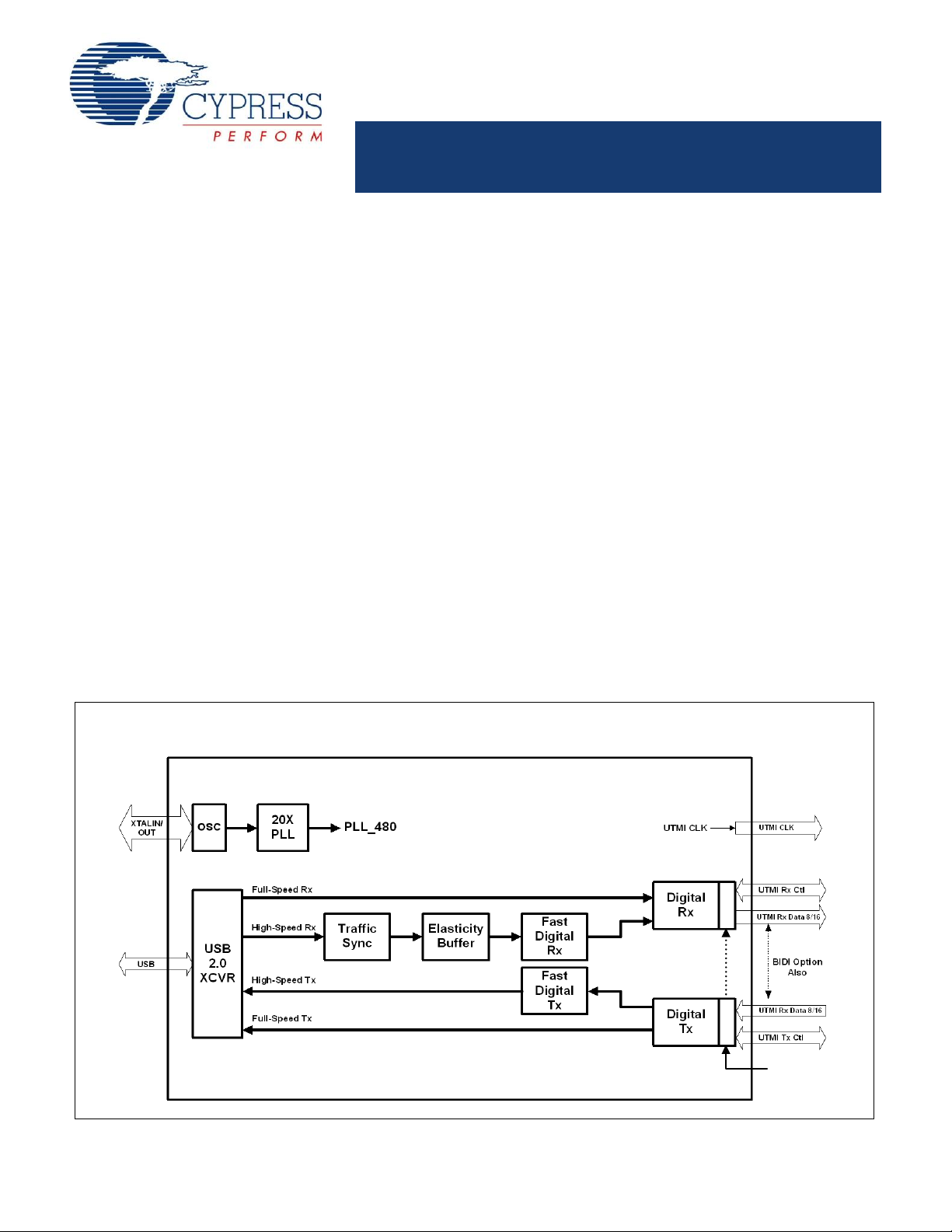
Logic Block Diagram
■ UTMI-compliant and USB 2.0 certified for device operation
■ Operates in both USB 2.0 High Speed (HS), 480 Mbits/second,
and Full Speed (FS), 12 Mbits/second
■ Optimized for Seamless Interface with Intel
cations Processors
■ Tri-state Mode enables sharing of UTMI Bus with other devices
■ Serial-to-Parallel and Parallel-to-Serial Conversions
■ 8-bit Unidirectional, 8-bit Bidirectional, or 16-bit Bidirectional
External Data Interface
■ Synchronous Field and EOP Detection on Receive Packets
■ Synchronous Field and EOP Generation on Transmit Packets
■ Data and Clock Recovery from the USB Serial Stream
■ Bit stuffing and unstuffing; Bit Stuff Error Detection
■ Staging Register to manage Data Rate variation due to Bit
stuffing and unstuffing
■ 16-bit 30 MHz and 8-bit 60 MHz Parallel Interface
■ Ability to switch between FS and HS terminations and signaling
■ Supports detection of USB Reset, Suspend, and Resume
■ Supports HS identification and detection as defined by the USB
2.0 Specification
®
Monahans Appli-
■ Supports transmission of Resume Signaling
■ 3.3V Operation
■ Two package options: 56-pin QFN and 56-pin VFBGA
■ All required terminations, including 1.5 Kohm pull up on
DPLUS, are internal to chip
■ Supports USB 2.0 Test Modes
The Cypress MoBL-USB TX2 is a Universal Serial Bus (USB)
specification revision 2.0 transceiver, serial and deserializer, to a
parallel interface of either 16 bits at 30 MHz or eight bits at 60
MHz. The MoBL-USB TX2 provides a high speed physical layer
interface that operates at the maximum allowable USB 2.0
bandwidth. This enables the system designer to keep the
complex high speed analog USB components external to the
digital ASIC. This decreases development time and associated
risk. A standard USB 2.0-certified interface is provided and is
compliant with Transceiver Macrocell Interface (UTMI) specification version 1.05 dated 3/29/2001.
This product is also optimized to seamlessly interface with
Monahans -P & -L applications processors. It has been characterized by Intel and is recommended as the USB 2.0 UTMI transceiver of choice for its Monahans processors. It is also capable
of tri-stating the UTMI bus, while suspended, to enable the bus
to be shared with other devices.
Two packages are defined for the family: 56-pin QFN and 56-pin
VFBGA.
The functional block diagram follows.
Cypress Semiconductor Corporation • 198 Champion Court • San Jose, CA 95134-1709 • 408-943-2600
Document #: 38-08052 Rev. *G Revised October 5, 2008
[+] Feedback
Page 2

CY7C68000A
Applications
Mobile Applications
■ Smart Phones
■ PDA Phones
■ Gaming Phones
■ MP3 players
■ Portable Media Players (PMP)
■ GPS Tracking Devices
Consumer Applications
■ Cameras
■ Scanners
■ DSL Modems
■ Memory Card Readers
Non-Consumer Applications
■ Networking
■ Wireless LAN
■ Home PNA
Functional Overview
The functionality of this chip is described in the following
sections:
USB Signaling Speed
The MoBL-USB TX2 operates at two of the rates defined in the
USB Specification 2.0, dated 4/27/2000.
■ Full speed, with a signaling bit rate of 12 Mbps
■ High speed, with a signaling bit rate of 480 Mbps
The MoBL-USB TX2 does not support the LS signaling rate of
1.5 Mbps.
Transceiver Clock Frequency
The MoBL-USB TX2 has an on-chip oscillator circuit that uses
an external 24 MHz (±100 ppm) crystal with the following characteristics:
■ Parallel resonant
■ Fundamental mode
■ 500 μW drive level
■ 27 to 33 pF (5% tolerance) load capacitors
An on-chip phase-locked loop (PLL) multiplies the 24 MHz oscillator up to 30 or 60 MHz, as required by the transceiver parallel
data bus. The default UTMI interface clock (CLK) frequency is
determined by the DataBus16_8 pin.
Buses
The two packages enable a 8- or 16-bit bidirectional data bus for
data transfers to a controlling unit.
Suspend and Tri-state Modes
When the MoBL-USB TX2 is not in use, the processor reduces
power consumption by putting it into Suspend mode using the
Suspend pin.
While in Suspend mode, Tri-state mode may be enabled, which
tri-states all outputs and IOs, enabling the UTMI interface pins to
be shared with other devices. This is valuable in mobile handset
applications, where GPIOs are at a premium. The outputs and
IOs are tri-stated ~50ns when Tri-state mode is enabled, and are
driven ~50ns when Tri-state mode is disabled. All inputs must not
be left floating while in Tri-state mode.
When resuming after a suspend, the PLL stabilizes approximately 200 μs after the suspend pin goes high.
Reset Pin
An input pin (Reset) resets the chip. This pin has hysteresis and
is active HIGH according to the UTMI specification. The internal
PLL stabilizes approximately 200 μs after V
has reached 3.3V.
CC
Line State
The Line State output pins LineState[1:0] are driven by combinational logic and may be toggling between the ‘J’ and the ‘K’
states. They are synchronized to the CLK signal for a valid
signal. On the CLK edge, the state of these lines reflect the state
of the USB data lines. Upon the clock edge the ‘0’ bit of the
LineState pins is the state of the DPLUS line and the ‘1’ bit of
LineState is the DMINUS line. When synchronized, the setup
and hold timing of the LineState is identical to the parallel data
bus.
Full-speed versus High-speed Select
The FS versus HS is done through the use of both XcvrSelect
and the TermSelect input signals. The TermSelect signal enables
the 1.5 Kohm pull up on to the DPLUS pin. When TermSelect is
driven LOW, a SE0 is asserted on the USB providing the HS
termination and generating the HS Idle state on the bus. The
XcvrSelect signal is the control that selects either the FS transceivers or the HS transceivers. By setting this pin to a ‘0’ the HS
transceivers are selected and by setting this bit to a’1’ the FS
transceivers are selected.
Document #: 38-08052 Rev. *G Page 2 of 15
[+] Feedback
Page 3
CY7C68000A
Operational Modes
The operational modes are controlled by the OpMode signals.
The OpMode signals are capable of inhibiting normal operation
of the transceiver and evoking special test
take effect immediately and take precedence over any pending
data operations. The transmission data rate when in OpMode
depends on the state of the XcvrSelect input.
OpMode[1:0] Mode Description
00 0 Normal operation
01 1 Non-driving
10 2 Disable Bit Stuffing and NRZI
encoding
11 3 Reserved
modes. These modes
Mode 0 enables the transceiver to operate with normal USB data
decoding and encoding.
Mode 1 enables the transceiver logic to support a soft disconnect
feature that tri-states both the HS and FS transmitters, and
removes any termination from the USB, making it appear to an
upstream port that the device is disconnected from the bus.
Mode 2 disables Bit Stuff and NRZI encoding logic so ‘1’s loaded
from the data bus becomes ‘J’s on the DPLUS/DMINUS lines
and ‘0’s become ‘K’s.
DPLUS/DMINUS Impedance Termination
The CY7C68000A does not require external resistors for USB
data line impedance termination or an external pull up resistor on
the DPLUS line. These resistors are incorporated into the part.
They are factory trimmed to meet the requirements of USB 2.0.
Incorporating these resistors also reduces the pin count on the
part.
Document #: 38-08052 Rev. *G Page 3 of 15
[+] Feedback
Page 4
CY7C68000A
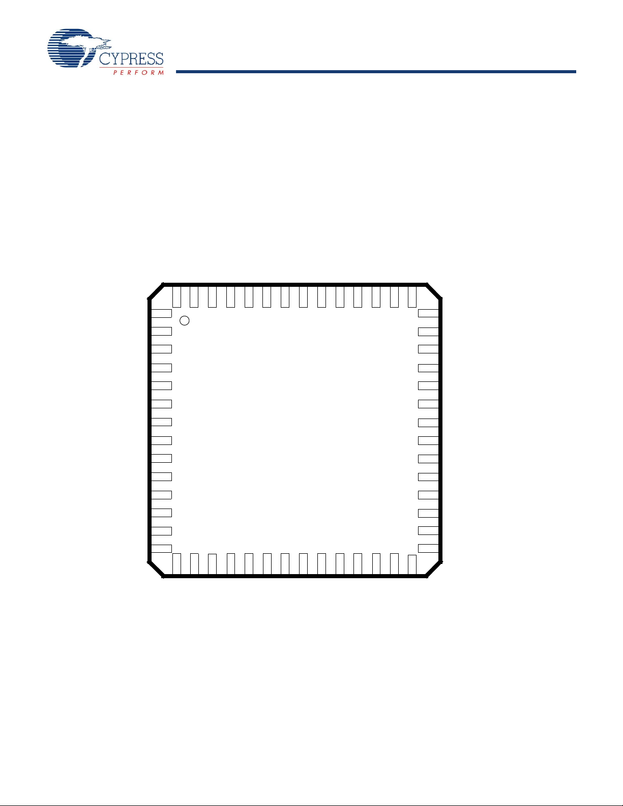
Pin Configurations
D4
D3
V
CC
D2
Reserved
D1
D0
CLK
DataBus16_8
Uni_bidi
GND
TXValid
V
CC
ValidH
28
27
26
25
24
23
22
21
20
19
18
17
16
15
43
44
45
46
47
48
49
50
51
52
53
54
55
56
1
2
3
4
5
6
7
8
9
10
11
12
13
14
42
41
40
39
38
37
36
35
34
33
32
31
30
29
GND
D5
Reserved
D6
D7
D8
D9
Reserved
D10
D11
V
CC
D12
GND
D13
TXReady
Suspend
Reset
AV
CC
XTALOUT
XTALIN
AGND
AV
CC
DPLUS
DMINUS
AGND
XcvrSelect
TermSelect
OpMode0
V
CC
D14
D15
Reserved
Tri_state
RXError
RXActive
RXValid
GND
LineState1
LineState0
V
CC
GND
OpMode1
CY7C68000A
56-pin QFN
The following pages illustrate the individual pin diagrams that are available in the 56-pin QFN and 56-pin VFBGA packages.
The packages offered use either an 8-bit (60 MHz) or 16-bit (30 MHz) bus interface.
Figure 1. CY7C68000A 56-pin QFN Pin Assignment
Document #: 38-08052 Rev. *G Page 4 of 15
[+] Feedback
Page 5
CY7C68000A
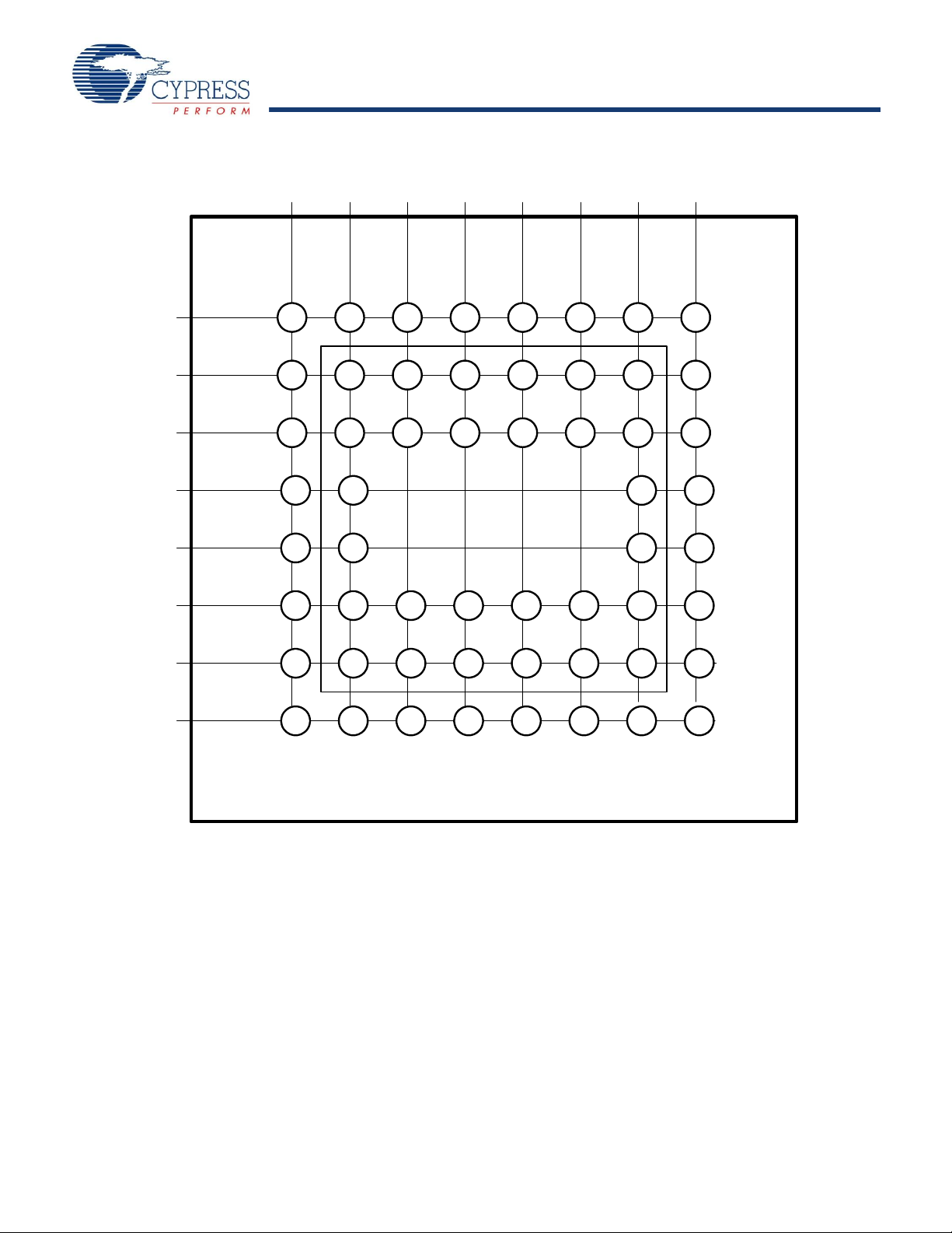
Figure 2. CY7C68000A 56-pin VFBGA Pin Assignment
12345678
A
B
C
D
E
F
G
H
1A 2A 3A 4A 5A 6A 7A 8A
1B 2B 3B 4B 5B 6B 7B 8B
1C 2C 3C 4C 5C 6C 7C 8C
1D 2D 7D 8D
1E 2E 7E 8E
1F 2F 3F 4F 5F 6F 7F 8F
1G 2G 3G 4G 5G 6G 7G 8G
1H 2H 3H 4H 5H 6H 7H 8H
Document #: 38-08052 Rev. *G Page 5 of 15
[+] Feedback
Page 6

CY7C68000A
Pin Descriptions
Note
1. Unused inputs should not be left floating. Tie either HIGH or LOW as appropriate. Outputs that are three-statable should only be pulled up or down to ensure
signals at power-up and in standby.
Table 1. Pin Descriptions
QFN VFBGA Name Type Default Description
4H1AVCC PowerN/AAnalog V
This signal provides power to the analog section of the chip.
CC
8H5AVCC PowerN/AAnalog VCC This signal provides power to the analog section of the chip.
7H4AGND PowerN/AAnalog Ground Connect to ground with as short a path as possible.
11 H8 AGND Power N/A Analog Ground Connect to ground with as short a path as possible.
9 H6 DPLUS I/O/Z Z USB DPLUS Signal Connect to the USB DPLUS signal.
10 H7 DMINUS I/O/Z Z USB DMINUS Signal Connect to the USB DMINUS signal.
49 G8 D0 I/O Bidirectional Data Bus This bidirectional bus is used as the entire data
48 G7 D1 I/O
46 G5 D2 I/O
bus in the 8-bit bidirectional mode or the least significant eight bits in the
16-bit mode. Under the 8-bit unidirectional mode, these bits are used as
inputs for data, selected by the RxValid signal.
44 G3 D3 I/O
43 G2 D4 I/O
41 F8 D5 I/O
39 F6 D6 I/O
38 F5 D7 I/O
37 F4 D8 I/O Bidirectional Data Bus This bidirectional bus is used as the upper eight
36 F3 D9 I/O
34 F1 D10 I/O
bits of the data bus when in the 16-bit mode, and not used when in the
8-bit bidirectional mode. Under the 8-bit unidirectional mode these bits
are used as outputs for data, selected by the TxValid signal.
33 G4 D11 I/O
31 E1 D12 I/O
29 D8 D13 I/O
27 G1 D14 I/O
26 E2 D15 I/O
50 A1 CLK Output Clock This output is used for clocking the receive and transmit parallel
data on the D[15:0] bus.
3 B2 Reset Input N/A Active HIGH Reset Resets the entire chip. This pin can be tied to V
through a 0.1-μF capacitor and to GND through a 100 K resistor for a
10-ms RC time constant.
12 B3 XcvrSelect Input N/A Transceiver Select This signal selects between the Full Speed (FS) and
the High Speed (HS) transceivers:
0: HS transceiver enabled
1: FS transceiver enabled
13 B4 TermSelect Input N/A Termination Select This signal selects between the Full Speed (FS) and
the High Speed (HS) terminations:
0: HS termination
1: FS termination
2 B1 Suspend Input N/A Suspend Places the CY7C68000A in a mode that draws minimal power
from supplies. Shuts down all blocks not necessary for Suspend/Resume
operations. While suspended, TermSelect must always be in FS mode
to ensure that the 1.5 Kohm pull up on DPLUS remains powered.
0: CY7C68000A circuitry drawing suspend current
1: CY7C68000A circuitry drawing normal current
[1]
CC
Document #: 38-08052 Rev. *G Page 6 of 15
[+] Feedback
Page 7

CY7C68000A
Table 1. Pin Descriptions (continued)
QFN VFBGA Name Type Default Description
24 B8 Tri_state Input Tri-state Mode Enable Places the CY7C68000A into Tri-state mode
which tri-states all outputs and IOs. Tri-state Mode can only be enabled
while suspended.
0: Disables Tri-state Mode
1: Enables Tri-state Mode
19 C2 LineState1 Output Line State These signals reflect the current state of the single-ended
receivers. They are combinatorial until a “usable” CLK is available then
they are synchronized to CLK. They directly reflect the current state of the
DPLUS (LineState0) and DMINUS (LineState1).
D– D+ Description
0 0 0: SE0
0 1 1: ‘J’ State
1 0 2: ‘K’ State
1 1 3: SE1
18 C1 LineState0 Output Line State These signals reflect the current state of the single-ended
receivers. They are combinatorial until a ‘usable’ CLK is available then
they are synchronized to CLK. They directly reflect the current state of the
DPLUS (LineState0) and DMINUS (LineState1).
D– D+ Description
00–0: SE0
01–1: ‘J’ State
10–2: ‘K’ State
11–3: SE1
15 B6 OpMode1 Input Operational Mode These signals select among various operational
modes.
10 Description
00–0: Normal Operation
01–1: Non-driving
10–2: Disable Bit Stuffing and NRZI encoding
11–3: Reserved
14 B5 OpMode0 Input Operational Mode These signals select among various operational
modes.
10 Description
00–0: Normal Operation
01–1: Non-driving
10–2: Disable Bit Stuffing and NRZI encoding
11–3: Reserved
54 A5 TXValid Input Transmit Valid This signal indicates that the data bus is valid. The asser-
tion of Transmit Valid initiates SYNC on the USB. The negation of Transmit Valid initiates EOP on the USB. The start of SYNC must be initiated
on the USB no less than one or no more that two CLKs after the assertion
of TXValid.
In HS (XcvrSelect = 0) mode, the SYNC pattern must be asserted on the
USB between 8- and 16-bit times after the assertion of TXValid is detected
by the Transmit State Machine.
In FS (Xcvr = 1), the SYNC pattern must be asserted on the USB no less
than one or more than two CLKs after the assertion of TXValid is detected
by the Transmit State Machine.
1 A8 TXReady Output Transmit Data Ready If TXValid is asserted, the SIE must always have
data available for clocking in to the TX Holding Register on the rising edge
of CLK. If TXValid is TRUE and TXReady is asserted at the rising edge
of CLK, the CY7C68000A loads the data on the data bus into the TX
Holding Register on the next rising edge of CLK. At that time, the SIE
should immediately present the data for the next transfer on the data bus
[1]
(continued)
.
Document #: 38-08052 Rev. *G Page 7 of 15
[+] Feedback
Page 8

CY7C68000A
Table 1. Pin Descriptions (continued)
QFN VFBGA Name Type Default Description
[1]
(continued)
21 A4 RXValid Output Receive Data Valid This signal indicates that the DataOut bus has valid
data. The Receive Data Holding Register is full and ready to be unloaded.
The SIE is expected to latch the DataOut bus on the clock edge.
22 B7 RXActive Output Receive Active This signal indicates that the receive state machine has
detected SYNC and is active.
RXActive is negated after a bit stuff error or an EOP is detected.
23 A6 RXError Output Receive Error
0 Indicates no error.
1 Indicates that a receive error has been detected.
56 A7 ValidH I/O ValidH This signal indicates that the high-order eight bits of a 16-bit data
word presented on the Data bus are valid. When DataBus16_8 = 1 and
TXValid = 0, Valid H is an output, indicating that the high-order receive
data byte on the Data bus is valid. When DataBus16_8 = 1 and TXValid
= 1, ValidH is an input and indicates that the high-order transmit data byte,
presented on the Data bus by the transceiver, is valid. When
DataBus16_8 = 0, ValidH is undefined. The status of the receive
low-order data byte is determined by RXValid and are present on D0–D7.
51 A2 DataBus16_8 Input Data Bus 16_8 This signal selects between 8- and 16-bit data transfers.
1–16-bit data path operation enabled. CLK = 30 MHz.
0–8-bit data path operation enabled. When Uni_Bidi = 0, D[8:15] are undefined. When Uni_Bidi =1, D[0:7] are valid on TxValid and D[8:15] are
valid on RxValid. CLK = 60 MHz
Note: DataBus16_8 is static after Power-on Reset (POR) and is only
sampled at the end of Reset.
6 H3 XTALIN Input N/A Crystal Input Connect this signal to a 24 MHz parallel-resonant, funda-
mental mode crystal and 30 pF capacitor to GND.
It is also correct to drive XTALIN with an external 24 MHz square wave
derived from another clock source.
5 H2 XTALOUT Output N/A Crystal Output Connect this signal to a 24 MHz parallel-resonant, funda-
mental mode crystal and 30 pF (nominal) capacitor to GND. If an external
clock is used to drive XTALIN, leave this pin open.
52 A3 Uni_Bidi Input Driving this pin HIGH enables the unidirectional mode when the 8-bit
interface is selected. Uni_Bidi is static after power-on reset (POR).
55 C6 V
17 C7 V
28 D7 V
32 E7 V
45 E8 V
CC
CC
CC
CC
CC
Power VCC. Connect to 3.3V power source.
Power N/A VCC. Connect to 3.3V power source.
Power N/A VCC. Connect to 3.3V power source.
Power N/A VCC. Connect to 3.3V power source.
Power N/A VCC. Connect to 3.3V power source.
53 C4 GND Ground N/A Ground.
16 C5 GND Ground N/A Ground.
20 C3 GND Ground N/A Ground.
30 D1 GND Ground N/A Ground.
42 D2 GND Ground N/A Ground.
47 G6 Reserved INPUT Connect pin to Ground.
40 F7 Reserved INPUT Connect pin to Ground.
35 F2 Reserved INPUT Connect pin to Ground.
25 C8 Reserved INPUT Connect pin to Ground.
Document #: 38-08052 Rev. *G Page 8 of 15
[+] Feedback
Page 9

CY7C68000A
Absolute Maximum Ratings
Note
2. Connected to the USB includes 1.5 Kohm internal pull up. Disconnected has the 1.5 Kohm internal pull up excluded.
Operating Conditions
Storage Temperature ................................. –65°C to +150°C
Ambient Temperature with Power Supplied ..... 0°C to +70°C
Supply Voltage to Ground Potential ...............–0.5V to +4.0V
DC Input Voltage to Any Input Pin ............................. 5.25 V
DC Voltage Applied to Outputs
in High-Z State ..................................... –0.5V to V
CC
+ 0.5V
TA (Ambient Temperature Under Bias) ............ 0°C to +70°C
Supply Voltage ...............................................+3.0V to +3.6V
Ground Voltage .................................................................0V
F
(Oscillator or Crystal Frequency) ... 24 MHz ± 100 ppm
OSC
...................................................................Parallel Resonant
Power Dissipation ....................................................630 mW
Static Discharge Voltage .......................................... > 2000V
Max Output Current, per IO pin ................................... 4 mA
Max Output Current, all 21–IO pins ............................84 mA
DC Characteristics
Table 2. DC Characteristics
Parameter Description Conditions Min Ty p Max Unit
V
CC
V
IH
V
IL
I
I
V
OH
V
OL
I
OH
I
OL
C
IN
C
LOAD
I
SUSP
I
CC
I
CC
t
RESET
Supply Voltage 3.0 3.3 3.6 V
Input High Voltage 2 5.25 V
Input Low Voltage –0.5 0.8 V
Input Leakage Current 0< VIN < V
Output Voltage High I
Output Low Voltage I
= 4 mA 2.4 V
OUT
= –4 mA 0.4 V
OUT
CC
±10 μA
Output Current High 4mA
Output Current Low 4mA
Input Pin Capacitance Except DPLUS/DMINUS/CLK 10 pF
DPLUS/DMINUS/CLK 15 pF
Maximum Output Capacitance Output pins 30 pF
Suspend Current Connected
Disconnected
[2]
[2]
228 273 μA
835μA
Supply Current HS Mode Normal operation OPMOD[1:0] = 00 175 mA
Supply Current FS Mode Normal operation OPMOD[1:0] = 00 90 mA
Minimum Reset time 1.9 ms
Document #: 38-08052 Rev. *G Page 9 of 15
[+] Feedback
Page 10
CY7C68000A
AC Electrical Characteristics
TCSU_MIN
TCH_MIN
TDSU_MIN
TDH_MIN
TCDO
TCCO
DataIn
DataOut
Control_Out
Control_In
CLK
USB 2.0 Transceiver
USB 2.0-compliant in FS and HS modes.
Timing Diagram
HS/FS Interface Timing - 60 MHz
Figure 3. 60 MHz Interface Timing Constraints
Table 3. 60 MHz Interface Timing Constraints Parameters
Parameter Description Min Typ Max Unit Notes
T
CSU_MIN
T
CH_MIN
T
DSU_MIN
T
DH_MIN
T
CCO
T
CDO
Minimum setup time for TXValid 4 ns
Minimum hold time for TXValid 1 ns
Minimum setup time for Data (transmit direction) 4 ns
Minimum hold time for Data (transmit direction) 1 ns
Clock to Control out time for TXReady, RXValid,
18ns
RXActive and RXError
Clock to Data out time (Receive direction) 1 8 ns
Document #: 38-08052 Rev. *G Page 10 of 15
[+] Feedback
Page 11

CY7C68000A
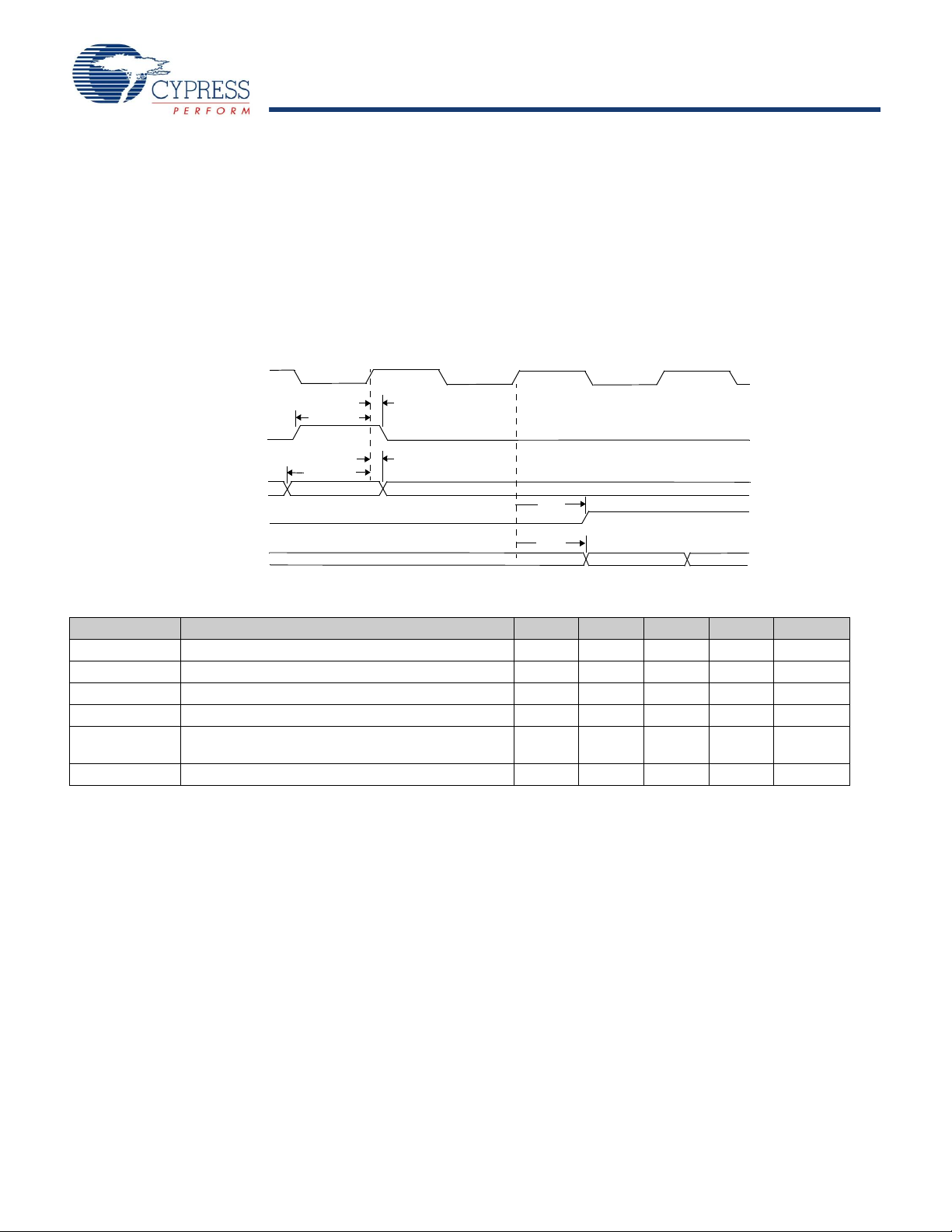
HS/FS Interface Timing - 30 MHz
TCSU_MIN
TCH_MIN
TDSU_MIN
TDH_MIN
TCVO
TCCO
DataIn
DataOut
Control_Out
Control_In
CLK
TCDO
TVSU_MIN
TVH_MIN
Ttssu Ttspd
Ttspd
Suspend
Tri-state
Output / IO XXXX Hi-Z
Figure 4. 30 MHz Timing Interface Timing Constraints
Table 4. 30 MHz Timing Interface Timing Constraints Parameters
Parameter Description Min Typ Max Unit Notes
T
CSU_MIN
T
CH_MIN
T
DSU_MIN
T
DH_MIN
T
CCO
T
CDO
T
VSU_MIN
T
VH_MIN
T
CVO
Minimum setup time for TXValid 16 ns
Minimum hold time for TXValid 1 ns
Minimum setup time for Data (Transmit direction) 16 ns
Minimum hold time for Data (Transmit direction) 1 ns
Clock to Control Out time for TXReady, RXValid,
120ns
RXActive and RXError
Clock to Data out time (Receive direction) 1 20 ns
Minimum setup time for ValidH (transmit Direction) 16 ns
Minimum hold time for ValidH (Transmit direction) 1 ns
Clock to ValidH out time (Receive direction) 1 20 ns
Figure 5. Tri-state Mode Timing Constraints
Table 5. Tri-state Mode Timing Constraints Parameters
Parameter Description Min Typ Max Unit Notes
T
tssu
T
tspd
Document #: 38-08052 Rev. *G Page 11 of 15
Minimum setup time for Tri-state 0 ns
Propagation Delay for Tri-State mode 50 ns
[+] Feedback
Page 12

CY7C68000A
Ordering Information
51-85187 *C
Ordering Code Package Type
CY7C68000A-56LFXC 56 QFN
CY7C68000A-56BAXC 56 VFBGA
CY3683 MoBL-USB TX2 Development Board
Package Diagrams
The MoBL-USB TX2 is available in two packages:
■ 56-pin QFN
■ 56-pin VFBGA
Figure 6. 56-Pin Quad Flatpack No Lead Package 8 x 8 mm (Sawn Version) LS56B
Document #: 38-08052 Rev. *G Page 12 of 15
[+] Feedback
Page 13

CY7C68000A
Package Diagrams (continued)
TOP VIEW
PIN A1 CORNER
0.50
3.50
5.00±0.10
BOTTOM VIEW
0.10(4X)
3.50
5.00±0.10
0.50
Ø0.15 M C A B
Ø0.05 M C
Ø0.30±0.05(56X)
A1 CORNER
-B-
-A-
1.0 max
0.160 ~0.260
0.080 C
0.45
SEATING PLANE
0.21
0.10 C
-C-
SIDE VIEW
5.00±0.10
5.00±0.10
REFERENCE JEDEC: MO-195C
PACKAGE WEIGHT: 0.02 grams
E
G
H
F
D
C
B
A
13265486
7856 2341
E
G
H
F
D
C
B
A
001-03901-*B
Note
3. Source for recommendations: EZ-USB FX2™ PCB Design Recommendations, http:///www.cypress.com/cfuploads/support/app_notes/FX2_PCB.pdf
High-Speed USB Platform Design Guidelines, http://www.usb.org/developers/docs/hs_usb_pdg_r1_0.pdf.
Figure 7. 56 VFBGA (5 x 5 x 1.0 mm) 0.50 Pitch, 0.30 Ball BZ56
PCB Layout Recommendations
Follow these recommendations to ensure reliable, high-performance operation
■ A four-layer impedance controlled board is required to maintain
[3]
.
signal quality
■ Specify impedance targets (ask your board vendor what they
can achieve)
■ To control impedance, maintain trace widths and trace spacing
to within written specifications
■ Minimize stubs to minimize reflected signals
■ Connections between the USB connector shell and signal
ground must be done near the USB connector
■ Bypass and flyback capacitors on VBus, near the connector,
are recommended
■ Keep DPLUS and DMINUS trace lengths within 2 mm of each
other in length, with preferred length of 20 to 30 mm
■ Maintain a solid ground plane under the DPLUS and DMINUS
traces. Do not split the plane under these traces
■ Do not place vias on the DPLUS or DMINUS trace routing
■ Isolate the DPLUS and DMINUS traces from all other signal
traces by no less than 10 mm
Document #: 38-08052 Rev. *G Page 13 of 15
[+] Feedback
Page 14

CY7C68000A
Quad Flat Package No Leads (QFN) Package
0.017” dia
Solder Mask
Cu Fill
Cu Fill
PCB Material
PCB Material
0.013” dia
Via hole for thermally connecting the
QFN to the circuit board ground plane.
This figure only shows the top three layers of the
circuit board: Top Solder, PCB Dielectric, and
the Ground Plane
Design Notes
Electrical contact of the part to the Printed Circuit Board (PCB)
is made by soldering the leads on the bottom surface of the
package to the PCB. Hence, special attention is required to the
heat transfer area below the package to provide a good thermal
bond to the circuit board. A Copper (Cu) fill is to be designed into
the PCB as a thermal pad under the package. Heat is transferred
from the MoBL-USB TX2 through the device’s metal paddle on
the package bottom. From here, heat is conducted to the PCB at
the thermal pad. It is then conducted from the thermal pad to the
PCB inner ground plane by an array of via. A via is a plated
through-hole in the PCB with a finished diameter of 13 mil. The
QFN’s metal die paddle must be soldered to the PCB’s thermal
pad. Solder mask is placed on the board top, over each via, to
resist solder flow into the via. The mask on the top side also
minimizes outgassing during the solder reflow process.
Figure 8. Cross section of the Area Underneath the QFN Package
For further information on this package design, refer to the application note “Surface Mount Assembly of AMKOR’s MicroLeadFrame (MLF) Technology.” Download this application note from
AMKOR’s website, by following this link:
http://www.amkor.com/products/notes_papers/MLFApp
Note.pdf. The application note provides detailed information on
board mounting guidelines, soldering flow, and rework process.
Figure 8 displays a cross-sectional area under the package. The
cross section is of only one via. The solder paste template needs
to be designed to enable at least 50 percent solder coverage.
The thickness of the solder paste template should be 5 mil. It is
recommended that ‘No Clean’, type 3 solder paste be used for
mounting the part. Nitrogen purge is recommended during
reflow.
Figure 9 is a plot of the solder mask pattern image of the
assembly (darker areas indicate solder).
Figure 9. Plot of the Solder Mask (White Area)
Document #: 38-08052 Rev. *G Page 14 of 15
[+] Feedback
Page 15

CY7C68000A
Document History Page
Document Title: CY7C68000A MoBL-USB™ TX2 USB 2.0 UTMI Transceiver
Document Number: 38-08052
REV. ECN NO.
Orig. of
Change
Submission
Date
Description of Change
** 285592 KKU See ECN New data sheet
*A 427959 TEH See ECN Addition of VFBGA Package information and Pinout, Removal of SSOP
Package. Edited text and moved figure titles to the top per new template
*B 470121 TEH See ECN Change from preliminary to final data sheet. Grammatical and formatting
changes
*C 476107 TEH See ECN This data sheet needs to be posted to the web site under NDA
*D 491668 TEH See ECN Addition of Tri-state Mode
*E 498415 TEH See ECN Update power consumption numbers
*F 567869 TEH See ECN Remove NDA requirement
*G 2587010 KKU/PYRS 10/13/08 Update Pin 6 description on Page 8
Update template
Sales, Solutions, and Legal Information
Worldwide Sales and Design Support
Cypress maintains a worldwide network of offices, solution centers, manufacturer’s representatives, and distributors. To find the office
closest to you, visit us at cypress.com/sales.
Products
PSoC psoc.cypress.com
Clocks & Buffers clocks.cypress.com
Wireless wireless.cypress.com
Memories memory.cypress.com
Image Sensors image.cypress.com
PSoC Solutions
General psoc.cypress.com/solutions
Low Power/Low Voltage psoc.cypress.com/low-power
Precision Analog psoc.cypress.com/precision-analog
LCD Drive psoc.cypress.com/lcd-drive
CAN 2.0b psoc.cypress.com/can
USB psoc.cypress.com/usb
© Cypress Semiconductor Corporation, 2004-2008. The information contained herein is subject to change without notice. Cypress Semiconductor Corporation assumes no responsibility for the use of
any circuitry other than circuitry embodied in a Cypress product. Nor does it convey or imply any license under patent or other rights. Cypress products are not warranted nor intended to be used for
medical, life support, life saving, critical control or safety applications, unless pursuant to an express written agreement with Cypress. Furthermore, Cypress does not authorize its products for use as
critical components in life-support systems where a malfunction or failure may reasonably be expected to result in significant injury to the user. The inclusion of Cypress products in life-support systems
application implies that the manufacturer assumes all risk of such use and in doing so indemnifies Cypress against all charges.
Any Source Code (software and/or firmware) is owned by Cypress Semiconductor Corporation (Cypress) and is protected by and subject to worldwide patent protection (United States and foreign),
United States copyright laws and international treaty provisions. Cypress hereby grants to licensee a personal, non-exclusive, non-transferable license to copy, use, modify, create derivative works of,
and compile the Cypress Sou rce Code and derivative works for the sole purpose of cr eating custom software and or firmware in support of licensee product to be used only in conjunction with a Cypress
integrated circuit as specified in the applicable agreement. Any reproduction, modification, translation, compilation, or representation of this Source Code except as specified above is prohibited without
the express written permission of Cypress.
Disclaimer: CYPRESS MAKES NO WARRANTY OF ANY KIND, EXPRESS OR IMPLIED, WITH REGARD TO THIS MATERIAL, INCLUDING, BUT NOT LIMITED TO, THE IMPLIED WARRANTIES
OF MERCHANTABILITY AND FITNESS FOR A PARTICULAR PURPOSE. Cypress reserves the right to make changes without further notice to the materials described herein. Cypress does not
assume any liability arising out of the application or use of any product or circuit described herein. Cypress does not authorize its products for use as critical components in life-support systems where
a malfunction or failure may reasonably be expected to result in significant injury to the user. The inclusion of Cypress’ product in a life-support systems application implies that the manufacturer
assumes all risk of such use and in doing so indemnifies Cypress against all charges.
Use may be limited by and subject to the applicable Cypress software license agreement.
Document #: 38-08052 Rev. *G Revised October 5, 2008 Page 15 of 15
MoBL-USB TX2 is a trademark of Cypress Semiconductor Corporation. Intel is a registered trademark of Intel Corporation. All product and company names mentioned in
this document are the trademarks of their respective holders.
All products and company names mentioned in this document may be the trademarks of their respective holders.
[+] Feedback
 Loading...