

Page 1
CY7C67300
EZ-Host™ Programmable Embedded USB Host and
Peripheral Controller with Automotive AEC Grade Support
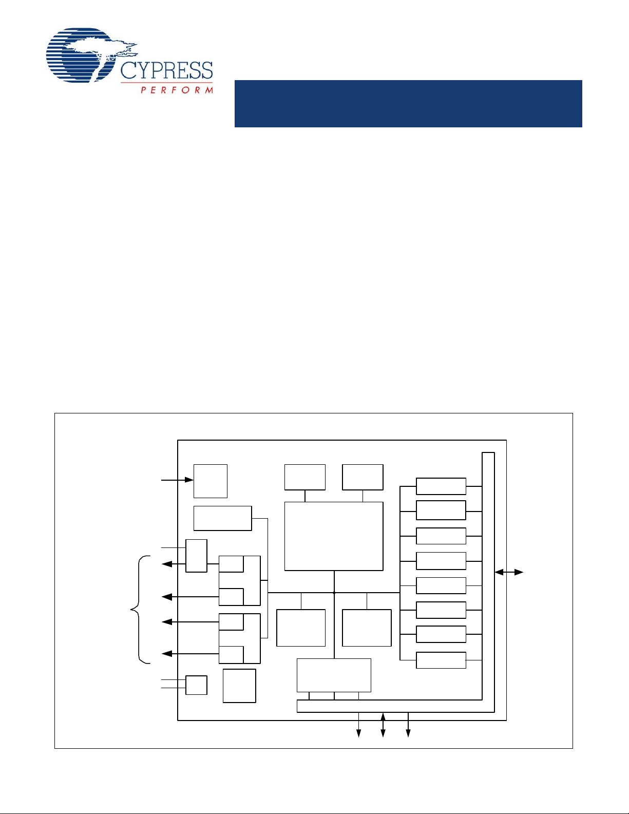
EZ-Host Features
Timer 0 Timer 1
Watchdog
Control
4Kx16
ROM BIOS
8Kx16
RAM
CY16
16-bit RISC CORE
External MEM I/F
(SRAM/ROM)
SIE1
USB-A
USB-B
SIE2
USB-A
USB-B
OTG
Host/
Peripheral
USB Ports
D+,D-
D+,D-
D+,D-
D+,D-
UART I/F
PWM
HSS I/F
I2C
EEPROM I/F
HPI I/F
IDE I/F
SPI I/F
nRESET
A[15:0]
D[15:0] CTRL[9:0]
CY7C67300
GPIO [31:0]
PLL
X1
X2
GPIO
SHARED INPUT/OUTPUT PINS
SHARED INPUT/OUTPUT PINS
Vbus, ID
Mobile
Power
Booster
CY7C67300 Block Diagram
■ Single chip programmable USB dual-role (Host/Peripheral)
controller with two configurable Serial Interface Engines (SIEs)
and four USB ports
■ Support for USB On-The-Go (OTG) protocol
■ On-chip 48 MHz 16-bit processor with dynamically switchable
clock speed
■ Configurable IO block supporting a variety of IO options or up
to 32 bits of General Purpose IO (GPIO)
■ 4K x 16 internal masked ROM containing built in BIOS that
supports a communication ready state with access to I
2
C™
EEPROM Interface, external ROM, UART, or USB
■ 8K x 16 internal RAM for code and data buffering
■ Extended memory interface port for external SRAM and ROM
■ 16-bit parallel Host Port Interface (HPI) with a DMA/mailbox
data path for an external processor to directly access all of the
on-chip memory and control on-chip SIEs
■ Fast serial port supports from 9600 baud to 2.0M baud
■ SPI support in both master and slave
■ On-chip 16-bit DMA/mailbox data path interface
■ Supports 12 MHz external crystal or clock
■ 3.3V operation
■ Automotive AEC grade option (–40°C to 85°C)
■ Package option—100-pin TQFP
Typical Applications
EZ-Host is a very powerful and flexible dual rol e USB co ntroller
that supports a wide variety of applications. It is primarily
intended to enable host capability in applications such as:
■ Set top boxes
■ Printers
■ KVM switches
■ Kiosks
■ Automotive applications
■ Wireless access points
Cypress Semiconductor Corporation • 198 Champion Court • San Jose, CA 95134-1709 • 408-943-2600
Document #: 38-08015 Rev. *J Revised July 28, 2008
[+] Feedback
Page 2

CY7C67300
Introduction
Note
1. Default interface location.
EZ-Host™ (CY7C67300) is Cypress Semiconductor’s first
full-speed, low cost multiport host/peripheral controller. EZ-Host
is designed to easily interface to most high performance CPUs
to add USB host functionality. EZ-Host has its own 16-bit RISC
processor to act as a coprocessor or operate in standalone
mode. EZ-Host also has a programmable IO interface block
allowing a wide range of interface options.
Functional Overview
An overview of the processor core components are presented in
this section.
Processor Core
EZ-Host has a general purpose 16-bit embedded RISC
processor that runs at 48 MHz.
Clocking
EZ-Host requires a 12 MHz source for clocking. Either an
external crystal or TTL level oscillator may be used. EZ-Host has
an internal PLL that produces a 48 MHz internal clock from the
12 MHz source.
Memory
EZ-Host has a built in 4K × 16 masked ROM and an 8K × 16
internal RAM. The masked ROM contains the EZ-Host BIOS.
The internal RAM can be used for program code or data.
Table 1. Interface Options for GPIO Pins
GPIO Pins HPI IDE PWM HSS SPI UART I2C OTG
GPIO31 SCL/SDA
GPIO30 SCL/SDA
GPIO29 OTGID
GPIO28 TX
GPIO27 RX
GPIO26 PWM3 CTS
GPIO25
GPIO24 INT IOREADY
GPIO23 nRD IOR
GPIO22 nWR IOW
GPIO21 nCS
GPIO20 A1 CS1
GPIO19 A0 CS0
GPIO18 A2 PWM2 RTS
GPIO17 A1 PWM1 RXD
GPIO16 A0 PWM0 TXD
GPIO15 D15 D15
GPIO14 D14 D14
GPIO13 D13 D13
GPIO12 D12 D12
GPIO11 D11 D11 MOSI
Interrupts
EZ-Host provides 128 interrupt vectors. The first 48 vectors are
hardware interrupts and the following 80 vectors are software
interrupts.
General Timers and Watchdog Timer
EZ-Host has two built in programmable timers and a Watchdog
timer. All three timers can generate an interrupt to the EZ-Host.
Power Management
EZ-Host has one main power saving mode, Sleep. Sleep mode
pauses all operations and provides the lowest power state.
Interface Descriptions
EZ-Host has a wide variety of interface options for connectivity.
With several interface options available, EZ-Host can act as a
seamless data transport between many different types of
devices.
See Table 1 and T able 2 on page 3 to understand how the inter-
faces share pins and which can coexist. Note that some interfaces have more then one possible port location selectable
through the GPIO control register [0xC006]. General guidelines
for interfaces are as follows:
■ HPI and IDE interfaces are mutually exclusive.
■ If 16-bit external memory is required, then HSS and SPI default
locations must be used.
2
■ I
C EEPROM and OTG do not conflict with any interfaces.
[1]
[1]
[1]
[1]
[1]
Document #: 38-08015 Rev. *J Page 2 of 99
[+] Feedback
Page 3

CY7C67300
Table 1. Interface Options for GPIO Pins (continued)
Note
2. Alternate interface location.
GPIO Pins HPI IDE PWM HSS SPI UART I2C OTG
GPIO10 D10 D10 SCK
GPIO9 D9 D9 nSSI
GPIO8 D8 D8 MISO
[1]
[1]
[1]
GPIO7 D7 D7
GPIO6 D6 D6
GPIO5 D5 D5
GPIO4 D4 D4
GPIO3 D3 D3
GPIO2 D2 D2
GPIO1 D1 D1
GPIO0 D0 D0
Table 2. Interface Options for External Memory Bus Pin s
MEM Pins HPI IDE PWM HSS SPI UART I2C OTG
D15 CTS
D14 RTS
D13 RXD
D12 TXD
D11 MOSI
D10 SCK
D9 nSSI
D8 MISO
[2]
[2]
[2]
[2]
[2]
[2]
[2]
[2]
D[7:0]
A[18:0]
CONTROL
USB Interface
EZ-Host has two built in Host/Peripheral SIEs and four USB transceivers that meet the USB 2.0 specification requirements for full and
low speed (high speed is not supported). In Host mode, EZ-Host supports four downstream ports, each support control, interrupt, bulk,
and isochronous transfers. In Peripheral mode, EZ-Host supports one peripheral port wi th eight endpoints for each of the two SI Es.
Endpoint 0 is dedicated as the control endpoint and only supports control transfers. Endpoints 1 though 7 support interrupt, bulk (up
to 64 bytes/packet), or isochronous transfers (up to 1023 Bytes/packet size). EZ-Host also supports a combination of Host and
Peripheral ports simultaneously as shown in Table 3.
Table 3. USB Port Configuration Options
Port Configurations Port 1A Port 1B Port 2A Port 2B
OTG OTG – – –
OTG + 2 Hosts OTG – Host Host
OTG + 1 Host OTG – Host –
OTG + 1 Host OTG – – Host
OTG + 1 Peripheral OTG – Peripheral –
OTG + 1 Peripheral OTG – – Peripheral
4 Hosts Host Host Host Host
3 Hosts Any Combination of Ports
2 Hosts Any Combination of Ports
1 Host Any Port
Document #: 38-08015 Rev. *J Page 3 of 99
[+] Feedback
Page 4

CY7C67300
Table 3. USB Port Configuration Options (continued)
Port Configurations Port 1A Port 1B Port 2A Port 2B
2 Hosts + 1 Peripheral Host Host Peripheral –
2 Hosts + 1 Peripheral Host Host – Peripheral
2 Hosts + 1 Peripheral Peripheral – Host Host
2 Hosts + 1 Peripheral – Peripheral Host Host
1 Host + 1 Peripheral Host – Peripheral –
1 Host + 1 Peripheral Host – – Peripheral
1 Host + 1 Peripheral – Host – Peripheral
1 Host + 1 Peripheral – Host Peri pheral –
1 Host + 1 Peripheral Peripheral – Host –
1 Host + 1 Peripheral Peripheral – – Host
1 Host + 1 Peripheral – Peripheral – Host
1 Host + 1 Peripheral – Peripheral Host –
2 Peripherals Peripheral – Peripheral –
2 Peripherals Peripheral – – Peripheral
2 Peripherals – Peripheral – Peripheral
2 Peripherals – Peripheral Peripheral –
1 Peripheral Any Port
USB Features
■ USB 2.0-compliant for full and low speed
■ Up to four downstream USB host ports
■ Up to two upstream USB peripheral ports
■ Configurable endpoint buffers (pointer and length), must reside
in internal RAM
■ Up to eight available peripheral endpoints (one control
endpoint)
■ Supports control, interrupt, bulk, and isochronous transfers
■ Internal DMA channels for each endpoint
■ Internal pull up and pull down resistors
■ Internal series termination resistors on USB data lines
USB Pins
Table 4. USB Interface Pins
Pin Name Pin Number
DM1A 22
DP1A 23
DM1B 18
DP1B 19
DM2A 9
DP2A 10
DM2B 4
DP2B 5
OTG Interface
EZ-Host has one USB port that is compatible with the USB
On-The-Go supplement to the USB 2.0 specification. The USB
OTG port has a various hardware features to support Session
Request Protocol (SRP) and Host Negotiation Protocol (HNP).
OTG is only supported on USB PORT 1A.
OTG Features
■ Internal charge pump to supply and control VBUS
■ VBUS valid status (above 4.4V)
■ VBUS status for 2.4V< VBUS <0.8V
■ ID pin status
■ Switchable 2K ohm internal discharge resistor on VBUS
■ Switchable 500 ohm internal pull up resistor on VBUS
■ Individually switchable internal pull up and pull down resistors
on the USB data lines
OTG Pins
Table 5. OTG Interface Pins
Pin Name Pin Number
DM1A 22
DP1A 23
OTGVBUS 11
OTGID 41
CSwitchA 13
CSwitchB 12
Document #: 38-08015 Rev. *J Page 4 of 99
[+] Feedback
Page 5

CY7C67300
External Memory Interface
0000 + PC[14:0]
1
0
PAGEx Register[5:0] + PC[12:0]
nXMEMSEL Pin
A[18:0]
PC = Program Counter
x = 1 or 2
A = CPU Address Bus
Where:
PAGE 1 Register Active Range = 8000h to 9FFFh
PAGE 2 Register Active Range = A000h to BFFFh
Note:
nXMEMSEL Pin Active Range = 8000h to BFFFh
EZ-Host provides a robust interface to a wide variety of external
memory arrays. All available external memory array locations
can contain either code or data. The CY16 RISC processor
directly addresses a flat memory space from 0x0000 to 0xFFFF.
External Memory Interface Features
■ Supports 8-bit or 16-bit SRAM or ROM
■ SRAM or ROM can be used for code or data space
■ Direct addressing of SRAM or ROM
■ Two external memory mapped page registers
External Memory Access Strobes
Access to external memory is sampled asynchronously on the
rising edge of strobes with a minimum of one wait state cycle. Up
to seven wait state cycles may be inserted for external memory
access. Each additional wait state cycle stretches the external
memory access time by 21 ns (you must be running in internal
memory when changing wait states). An external memory device
with 12 ns access time is necessary to support 48 MHz code
execution.
Page Registers
EZ-Host allows extended data or program code to be stored in
external SRAM, or ROM. The total size of extended memory can
be up to 512K bytes. The CY16 processor can access extended
memory via two address regions of 0x8000-0x9FFF and
0xA000-0xBFFF. The page register 0xC018 can be used to
control the address region 0x8000-0x9FFF and the page register
0xC01A controls the address region of 0xA000-0xBFFF.
Figure 1 illustrates that when the nXMEMSEL pin is asserted the
upper CPU address pins are driven by the contents of the Page
x registers.
Figure 1. Page n Registers External Address Pins Logic
Merge Mode
Merge modes enabled through the External Memory Control
register [0xC03A] allow combining of external memory regions in
accordance with the following:
■ nXMEMSEL is active from 0x8000 to 0xBFFF
■ nXRAMSEL is active from 0x4000 to 0x7FFF when RAM Merge
is disabled; nXRAMSEL is active from 0x4000 to 0xBFFF when
RAM Merge is enabled
■ nXROMSEL is active from 0xC100 to 0xDFFF when ROM
Merge is disabled; nXROMSEL is active from 0x8000 to
0xDFFF (excluding the 0xC000 to 0xC0FF area) when ROM
Merge is enabled
Program Memory Hole Description
Code residing in the 0xC000-0xC0FF address space is not
accessible by the CPU.
DMA to External Memory Prohibited
EZ-Host supports an internal DMA engine to rapidly move data
between different functional blocks within the chip. This DMA
engine is used for SIE1, SIE2, HPI, SPI, HSS, and IDE but it can
only transfer data between the specified block and internal RAM
or ROM. Setting up the DMA engine to transfer to or from an
external memory space might result in internal RAM data
corruption because the hardware (for example,
HSS/HPI/SIE1/SIE2/IDE) does not explicitly check the address
range. For example, setting up a DMA transfer to external
address 0x8000 might result in a DMA transfer into address
0x0000.
External Memory Related Resource Considerations:
■ By default A[18:15] are not available for general addressing
and are driven high on power up. The Upper Address Enable
register must be written appropriately to enable A[18:15] for
general addressing purposes.
■ 47K ohm external pull up on pin A15 for 12 MHz crystal
operation.
■ During the 3 ms BIOS boot procedure the CPU external
memory bus is active.
■ ROM boot load value 0xC3B6 located at 0xC100.
■ HPI, HSS, SPI, SIE1, SIE2, and IDE cannot DMA to external
memory arrays.
■ Page 1 banking is always enabled and is in effect from 0x8000
to 0x9FFF.
■ Page 2 banking is always enabled and is in effect from 0xA000
to 0xBFFF .
■ CPU memory bus strobes may wiggle when chip selects are
inactive.
Document #: 38-08015 Rev. *J Page 5 of 99
[+] Feedback
Page 6
CY7C67300
External Memory Interface Pins
EZ-Host
CY7C67300
External Memory Array
64K x 8
A[15:0]
nWR
nRD
nXRAMSEL
A[15:0]
WE
OE
CE
D[7:0] D[7:0]
Interfacing to 64K x 8 External Memory Array
EZ-Host
CY7C67300
External Memory Array
Up to 256k x 16
A[18:1]
nBEL
nBEH
nWR
nRD
nXMEMSEL
A[17:0]
BLE
WE
OE
CE
D[15:0] D[15:0]
Up to 256k x 16 External Code/Data (Page Mode)
BHE
Table 6. External Memory Interf ace Pins
Pin Name Pin Number
nWR 64
nRD 62
nXMEMSEL (optional nCS) 34
nXROMSEL (ROM nCS) 35
nXRAMSEL (RAM nCS) 36
A18 95
A17 96
A16 97
A15 38
A14 33
A13 32
A12 31
A11 30
A10 27
A9 25
A8 24
A7 20
A6 17
A5 8
A4 7
A3 3
A2 2
A1 1
nBEL/A0 99
nBEH 98
D15 67
D14 68
D13 69
D12 70
D11 71
D10 72
D9 73
D8 74
D7 76
D6 77
D5 78
D4 79
Table 6. External Memory Interface Pins (continued)
Pin Name Pin Number
D3 80
D2 81
D1 82
D0 83
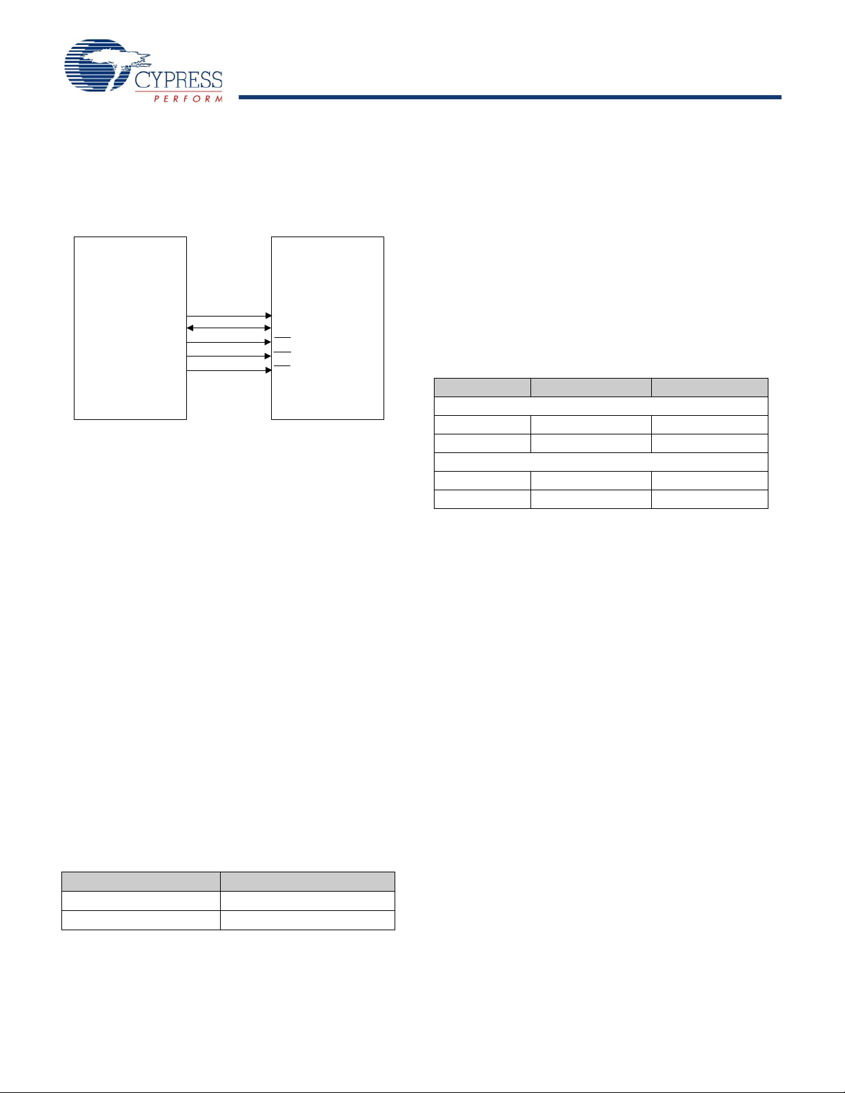
External Memory Interface Block Diagrams
Figure 2 illustrates how to connect a 64k × 8 memory array
(SRAM/ROM) to the EZ-Host external memory interface.
Figure 2. Interfacing to 64k × 8 Memory Array
Figure 3 illustrates the interface for connecting a 16-bit ROM or
16-bit RAM to the EZ-Host external memory interface. In 16-bit
mode, up to 256K words of external ROM or RAM are supported.
Note that the address lines do not map directly.
Figure 3. Interfacing up to 256k × 16 for External Code/Data
Document #: 38-08015 Rev. *J Page 6 of 99
[+] Feedback
Page 7
CY7C67300
Figure 4 illustrates the interface for connecting an 8-bit ROM or
EZ-Host
CY7C67300
External Memory Array
Up to 512k x8
A[18:0]
nWR
nRD
nXMEMSEL
A[18:0]
WE
OE
CE
D[7:0] D[7:0]
Up to 512k x 8 External Code/Data (Page Mode)
8-bit RAM to the EZ-Host external memory interface. In 8-bit
mode, up to 512K bytes of external ROM or RAM are supported.
Figure 4. Interfacing up to 512k × 8 for External Code/Data
General Purpose IO Interface (GPIO)
EZ-Host has up to 32 GPIO signals available. Several other
optional interfaces use GPIO pins as well and may reduce the
overall number of available GPIOs.
GPIO Description
All Inputs are sampled asynchronously with state changes
occurring at a rate of up to two 48 MHz clock cycles. GPIO pins
are latched directly into registers, a single flip-flop.
Unused Pin Descriptions
Ensure to tristate unused USB pins with the D+ line pulled high
through the internal pull up resistor and the D– line pu lled low
through the internal pull down resistor.
Configure unused GPIO pins as outputs so they are driven low.
UART Interface
EZ-Host has a built in UART interface. The UART interface
supports data rates from 900 to 115.2K baud. It can be used as
a development port or for other interface requirements. The
UART interface is exposed through GPIO pins.
UART Features
■ Supports baud rates of 900 to 115.2K
■ 8-N-1
UART Pins.
Table 7. UART Interface Pins
Pin Name Pin Number
TX 42
RX 43
I2C EEPROM Interface
EZ-Host provides a master-only I2C interface for external serial
EEPROMs. The serial EEPROM can be used to store application
specific code and data. Use the I
of EEPROM, it is not a general I
2
C interface for loading code out
2
C interface. The I2C EEPROM
interface is a BIOS implementation and is exposed through
GPIO pins. Refer to the BIOS documentation for additional
details on this interface.
I2C EEPROM Features
■ Supports EEPROMs up to 64 KB (512K bit)
■ Auto-detection of EEPROM size
I2C EEPROM Pins
Table 8. I2C EEPROM Interface Pins
Pin Name Pin Number GPIO Number
SMALL EEPROM
SCK 39 GPIO31
SDA 40 GPIO30
LARGE EEPROM
SCK 40 GPIO30
SDA 39 GPIO31
Serial Peripheral Interface
EZ-Host provides a SPI interface for added connectivity. EZ-Host
may be configured as either an SPI master or SPI slave. The SPI
interface can be exposed through GPIO pins or the External
Memory port.
SPI Features
■ Master or slave mode operation
■ DMA block transfer and PIO byte transfer modes
■ Full duplex or half duplex data communication
■ 8-byte receive FIFO and 8-byte transmit FIFO
■ Selectable master SPI clock rates from 250 kHz to 12 MHz
■ Selectable master SPI clock phase and polarity
■ Slave SPI signaling synchronization and filtering
■ Slave SPI clock rates up to 2 MHz
■ Maskable interrupts for block and byte transfer modes
■ Individual bit transfer for non-byte aligned seria l communi-
cation in PIO mode
■ Programmable delay timing for the active/inactive master SPI
clock
■ Auto or manual control for master mode slave select signal
■ Complete access to internal memory
Document #: 38-08015 Rev. *J Page 7 of 99
[+] Feedback
Page 8

CY7C67300
SPI Pins
The SPI port has a few different pin location options as shown in
Table 9. The port location is selectable via the GPIO control
register [0xC006].
Table 9. SPI Interface Pins
Pin Name Pin Number
Default Location
nSSI 56 or 65
SCK 61
MOSI 60
MISO 66
Alternate Location
nSSI 73
SCK 72
MOSI 71
MISO 74
HSS Pins
The HSS port has a few different pin location options as shown
in Table 10. The port location is selectable via the GPIO control
register [0xC006].
Ta bl e 10. HSS Interface Pin s
Pin Name Pin Number
Default Location
CTS 44
RTS 53
RXD 54
TXD 55
Alternate Location
CTS 67
RTS 68
RXD 69
TXD 70
High-Speed Serial Interface
EZ-Host provides an HSS interface. The HSS interface is a
programmable serial connection with baud rate from 9600 baud
to 2.0M baud. The HSS interface supports both byte and block
mode operations and also hardware and software handshaking.
Complete control of EZ-Host can be accomplished through this
interface via an extensible API and communication protocol. The
HSS interface can be exposed through GPIO pins or the External
Memory port.
HSS Features
■ 8 bits, no parity code
■ Programmable baud rate from 9600 baud to 2M baud
■ Selectable 1- or 2-stop bit on transmit
■ Programmable inter-character gap timing for Block Transmit
■ 8-byte receive FIFO
■ Glitch filter on receive
■ Block mode transfer directly to/from EZ-Host internal memory
(DMA transfer)
■ Selectable CTS/RTS hardware signal handshake protocol
■ Selectable XON/XOFF software handshake protocol
■ Programmable Receive interrupt, Block Transfer Done inter-
rupts
■ Complete access to internal memory
Programmable Pulse/PWM Interface
EZ-Host has four built in PWM output channels. Ea ch channel
provides a programmable timing generator sequence that can be
used to interface to various image sensors or other applications.
The PWM interface is exposed through GPIO pins.
Programmable Pulse/PWM Features
■ Four independent programmable waveform generators
■ Programmable predefined frequencies ranging from 5.90 KHz
to 48 MHz
■ Configurable polarity
■ Continuous and one-shot mode available
Programmable Pulse/PWM Pins.
Table 11. PWM Interface Pins
Pin Name Pin Number
PWM3 44
PWM2 53
PWM1 54
PWM0 55
Document #: 38-08015 Rev. *J Page 8 of 99
[+] Feedback
Page 9

CY7C67300
Host Port Interface
Notes
3. HPI_INT is for the Outgoing Mailbox interrupt.
4. HPI strobes are negative logic sampled on rising edge.
EZ-Host has an HPI interface. The HPI interface provides DMA
access to the EZ-Host internal memory by an external host, plus
a bidirectional mailbox register for supporting high level communication protocols. This port is designed to be the primary
high-speed connection to a host processor. Complete control of
EZ-Host can be accomplished through this interface via an
extensible API and communication protocol. Other than the
hardware communication protocols, a host processor has
identical control over EZ-Host whether connecting to the HPI o r
HSS port. The HPI interface is exposed through GPIO pins.
HPI Features
■ 16-bit data bus interface
■ 16 MB/s throughput
■ Auto-increment of address pointer for fast block mode transfers
■ Direct memory access (DMA) to internal memory
■ Bidirectional Mailbox register
■ Byte swapping
■ Complete access to internal memory
■ Complete control of SIEs through HPI
■ Dedicated HPI status register
HPI Pins
Table 12. HPI Interface Pins
Pin Name Pin Number
INT 46
nRD 47
nWR 48
nCS 49
A1 50
A0 52
D15 56
D14 57
D13 58
D12 59
[3, 4]
Ta bl e 12. HPI Interface Pin s (continued)
[3, 4]
D11 60
D10 61
D9 65
D8 66
D7 86
D6 87
D5 89
D4 90
D3 91
D2 92
D1 93
D0 94
The two HPI address pins are used to address one of four
possible HPI port registers as shown in Table 13.
Table 13. HPI Addressing
HPI A[1:0] A1 A0
HPI Data 0 0
HPI Mailbox 0 1
HPI Address 1 0
HPI Status 1 1
IDE Interface
EZ-Host has an IDE interface. The IDE interface supports PIO
mode 0-4 as specified in the Information Technology-AT
Attachment–4 with Packet Interface Extension (ATA/ATAPI-4)
Specification, T13/1153D Rev 18. There is no need for firmware
to use programmable wait states. The CPU read/write cycle is
automatically extended as needed for direct CPU to IDE
read/write accesses.
The EZ-Host IDE interface also has a BLOCK transfer mode that
allows EZ-Host to read/write large blocks of data to/from the IDE
data register and move it to/from the EZ-Host on-chip memory
directly without intervention of the CPU. The IDE interface is
exposed through GPIO pins. Table 14 on page 10 lists the
achieved throughput for maximum block mode data transfer rate
(with IDE_IORDY true) for the various IDE PIO modes.
Document #: 38-08015 Rev. *J Page 9 of 99
[+] Feedback
Page 10
CY7C67300
Table 14. IDE Throughput
VBUS
D1
D2
C1
C2
CSWITCHA
CSWITCHB
OTGVBUS
CY7C67300
Mode
ATA/ATAPI-4
Min Cycle Time
Actual
Min Cycle Time
ATA/ATPI-4
Max Transfer Rate
PIO Mode 0 600 ns 30T = 625 ns 3.33 MB/s 3.2 MB/s
PIO Mode 1 383 ns 20T = 416.7 ns 5.22 MB/s 4.8 MB/s
PIO Mode 2 240 13T = 270.8 ns 8.33 MB/s 7.38 MB/s
PIO Mode 3 180 ns 10T = 208.3 ns 11.11 MB/s 9.6 MB/s
PIO Mode 4 120 ns 8T = 166.7 ns 16.67 MB/s 12.0 MB/s
T = System clock period = 1/48 MHz.
Actual
Max Transfer Rate
IDE Features
■ Programmable IO mode 0–4
■ Block mode transfers
■ Direct memory access to/from internal memory through the IDE
data register
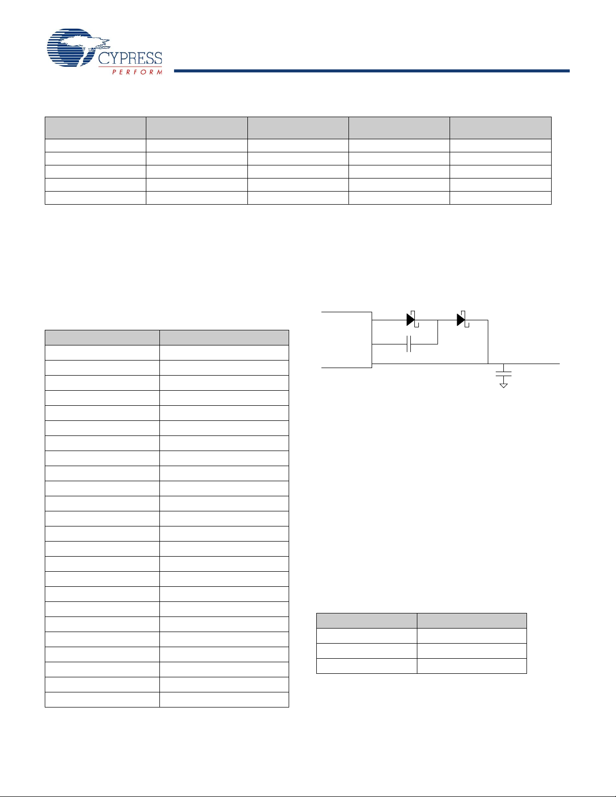
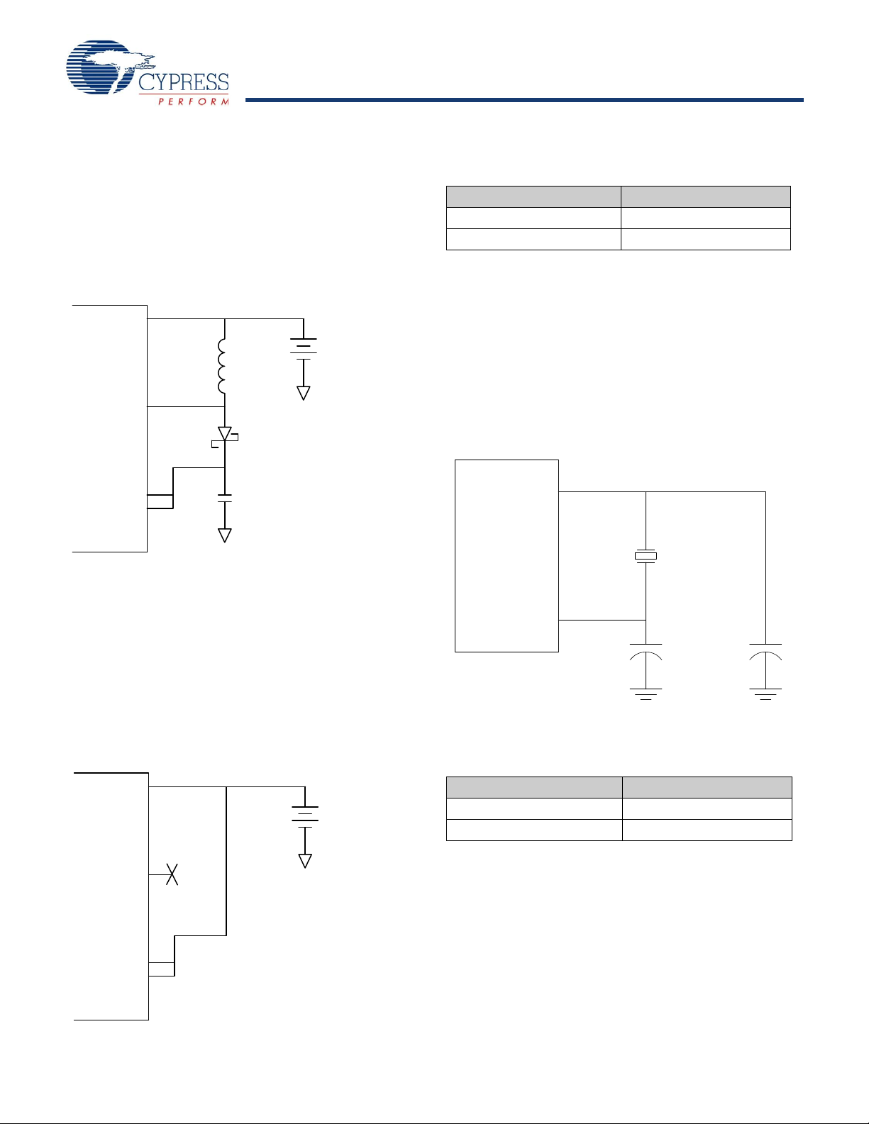
Charge Pump Interface
VBUS for the USB OTG port can be produced by EZ-Host using
its built in charge pump and some external components. Ensure
the circuit connections look similar to the following diagram.
Figure 5. Charge Pump
IDE Pins
Table 15. IDE Interface Pins
Pin Name Pin Number
IORDY 46
IOR 47
IOW 48
CS1 50
CS0 52
A2 53
A1 54
A0 55
D15 56
D14 57
D13 58
D12 59
Component details:
■ D1 and D2: Schottky diodes with a current rating greater than
60 mA
■ C1: Ceramic capacitor with a capacitance of 0.1 µF
■ C2: Make capacitor value no more that 6.5 µF since that is the
maximum capacitance allowed by the USB OTG specifications
for a dual role device. The minimum value of C2 is 1 µF. There
are no restrictions on the type of capacitor for C2.
If the VBUS charge pump circuit is not to be used, CSWITCHA,
CSWITCHB, and OTGVBUS can be left unconnected.
D11 60
D10 61
D9 65
D8 66
D7 86
D6 87
D5 89
D4 90
D3 91
D2 92
Charge Pump Features
■ Meets OTG Supplement Requirements, see Table 134, DC
Characteristics: Charge Pump on page 84 for details.
Charge Pump Pins
Table 16. Charge Pump Interface Pins
Pin Name Pin Number
OTGVBUS 1 1
CSwitchA 13
CSwitchB 12
D1 93
D0 94
Document #: 38-08015 Rev. *J Page 10 of 99
[+] Feedback
Page 11
CY7C67300
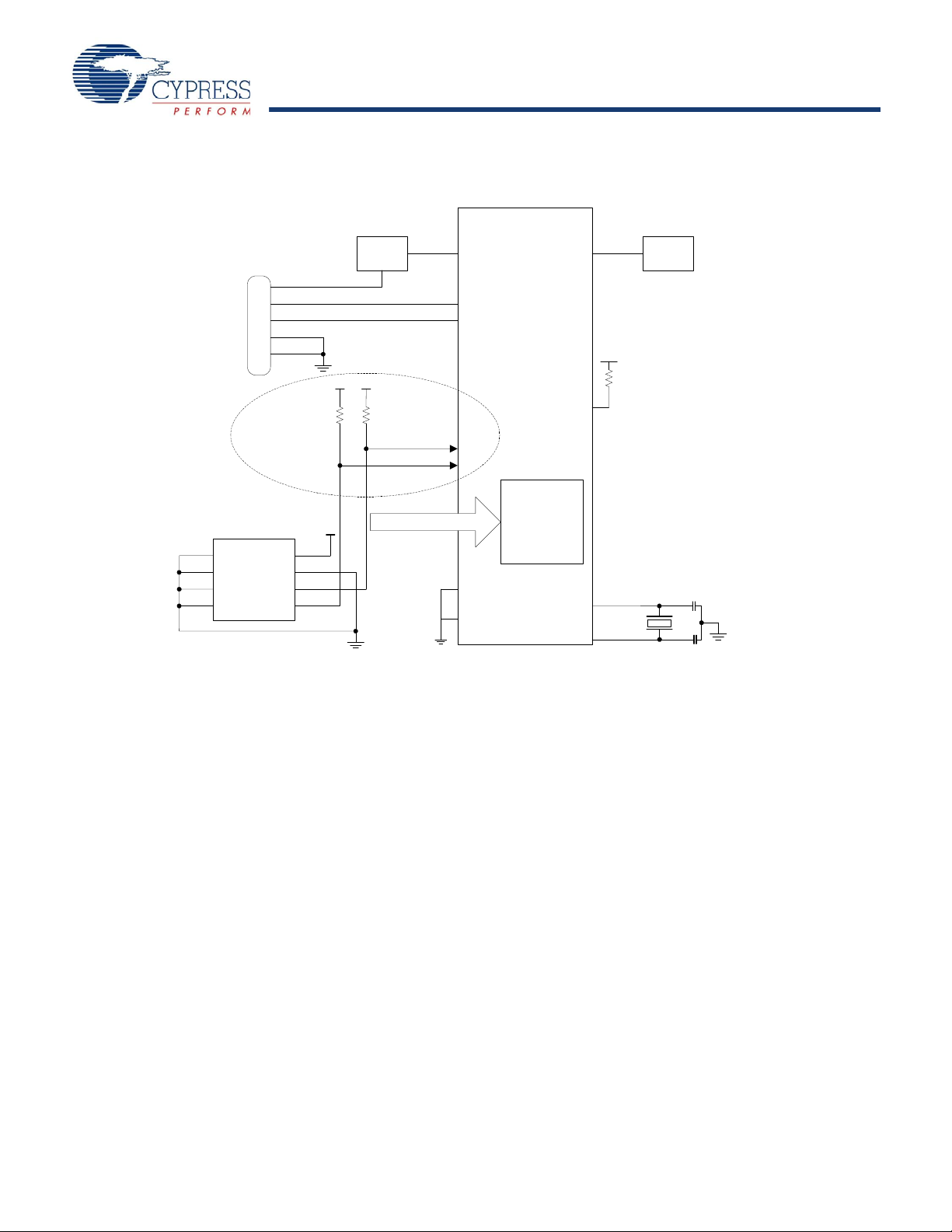
Booster Interface
BOOSTVcc
VSWITCH
VCC
AVCC
C1
D1
L1
3.3V
2.7V to 3.6V
Power Supply
BOOSTVcc
VSWITCH
VCC
AVCC
3.0V to 3.6V
Power Supply
Y1
C1 = 22 pF
C2 = 22 pF
CY7C67300
XTALIN
XTALOUT
12MHz
Parallel Resonant
Fundamental Mode
500uW
20-33pf ±5%
EZ-Host has an on chip power booster circuit for use with power
supplies that range between 2.7V and 3.6 V. The booster circuit
boosts the power to 3.3V nominal to supply power for the entire
chip. The booster circuit requires an external inductor, diode, and
capacitor. During power down mode, the circuit is disabled to
save power. Figure 6 shows how to connect the booster circuit.
Booster Pins
Table 17. Charge Pump Interface Pins
Pin Name Pin Number
BOOSTVcc 16
VSWITCH 14
Figure 6. Power Supply Connection With Booster
Component details:
■ L1: Inductor with inductance of 10 µH and a current rating of at
least 250 mA
■ D1: Schottky diode with a current rating of at least 250 mA
■ C1: Tant alum or ceramic capacitor with a capacitance of at least
2.2 µF
Figure 7 shows how to connect the power supply when the
booster circuit is not being used.
Crystal Interface
The recommended crystal circuit to be used with EZ-Host is
shown in Figure 8 If an oscillator is used instead of a crystal
circuit, connect it to XTALIN and leave XTALOUT unconnected.
For further information about the crystal requirements, see Table
132, Crystal Requirements on page 83.
Noted that the CLKSEL pin (pin 38) is sampled after reset to
determine what crystal or clock source frequency is used. For
normal operation, 12 MHz is required so the CLKSEL pin must
have a 47K ohm pull up resistor to V
Figure 8. Crystal Interface
CC.
.
Figure 7. Power Supply Connection Without Booster
Crystal Pins
Table 18. Crystal Pins
Pin Name Pin Number
XT ALIN 29
XT ALOUT 28
Document #: 38-08015 Rev. *J Page 11 of 99
[+] Feedback
Page 12

CY7C67300
Boot Configuration Interface
EZ-Host can boot into any one of four modes. The mode it boots
into is determined by the TTL voltage level of GPIO[31:30] at the
time nRESET is deasserted. Table 19 shows the different boot
pin combinations possible. After a reset pin event occurs, the
BIOS bootup procedure executes for up to 3 ms. GPIO[31:30]
are sampled by the BIOS during bootup only. Af ter bootup these
pins are available to the application as GPIOs.
Table 19. Boot Configuration Interface
GPIO31
(Pin 39)
0 0 Host Port Interface (HPI)
0 1 High-Speed Serial (HSS)
1 0 Serial Peripheral Interface (SPI,
11I
Ensure that GPIO[31:30] is pulled high or low as needed using
resistors tied to V
ohms and 15K ohms. Do not tie GPIO[31:30] directly to V
GND. Note that in standalone mode, the pull ups on those two
pins are used for the serial I2C EEPROM (if implemented). Make
sure that the resistors used for these pull ups conform to the
serial EEPROM manufacturer's requirements.
If any mode other then standalone is chosen, EZ-Host is in
coprocessor mode. The device powers up with the appropria te
communication interface enabled according to i ts boot p ins and
waits idle until a coprocessor communicates with it. See the
BIOS documentation for greater detail of the boot process.
GPIO30
(Pin 40)
CC
Boot Mode
slave mode)
2
C EEPROM (Standalone Mode)
or GND with resistor values between 5K
or
CC
Operational Modes
The operational modes are discussed in the following sections.
Coprocessor Mode
EZ-Host can act as a coprocessor to an external host processor.
In this mode, an external host processor drives EZ-Host and is
the main processor rather then EZ-Host’s own 16-bit internal
CPU. An external host processor may interface to EZ-Host
through one of the following three interfaces in coprocessor
mode:
■ HPI mode, a 16 bit parallel interface with up to 16 MB transfer
rate
■ HSS mode, a serial interface with up to 2M baud transfer rate
■ SPI mode, a serial interface with up to 2 Mb/s transfer rate
At bootup GPIO[31:30] determine which of these three interfaces
are used for coprocessor mode. See Table 19 for details.
Bootloading begins from the selected interface after POR + 3 ms
of BIOS bootup.
Standalone Mode
In standalone mode, there is no external processor connected to
EZ-Host. Instead, EZ-Host’s own internal 16-bit CPU is the main
processor and firmware is typically downloaded from an
EEPROM. Optionally, firmware may also be downloaded via
USB. See Table 19 for booting into standalone mode.
After booting into standalone mode (GPIO[31:30] = ‘11’), the
following pins are affected:
■ GPIO[31:30] are configured as output pins to examine the
EEPROM contents
■ GPIO[28:27] are enabled for debug UART mode
■ GPIO[29] is configured for as OTGID for OTG applications on
PORT1A
❐ If OTGID is logic 1 then PORT1A (OTG) is configured as a
USB peripheral
❐ If OTGID is logic 0 then PORT1A (OTG) is configured as a
USB host
■ Ports 1B, 2A, and 2B default as USB peripheral ports
■ All other pins remain INPUT pins.
Document #: 38-08015 Rev. *J Page 12 of 99
[+] Feedback
Page 13
CY7C67300
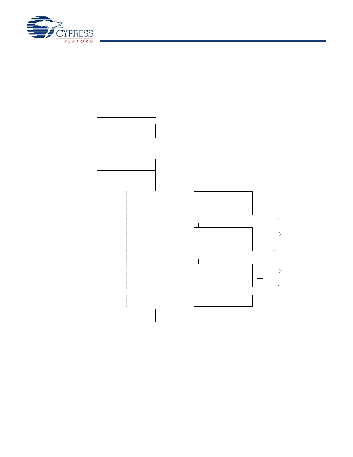
Minimum Hardware Requirements for Standalone Mode – Peripheral Only
EZ-Host
CY7C67300
GPIO[30]
GPIO[31]
SCL*
SDA*
10k
Bootstrap Options
Bootloading Firmware
*Bootloading begins after POR + 3ms BIOS bootup
Vcc
10k
Vcc
A2
GND
A0
A1
SCL
SDA
VCC
WP
VCC
Up to 64k x8
EEPROM
*GPIO[31:30] 31 30
Up to 2k x8 SCL SDA
>2k x8 to 64k x8 SDA SCL
Int. 16k x8
Code / Data
XOUT
XIN
12MHz
22pf
22pf
nRESET
Reset
Logic
*
Parallel Resonant
Fundamental Mode
500uW
20-33pf ±5%
VCC, AVCC,
BoostVCC
VReg
DMinus
DPlus
Standard-B
or Mini-B
D+
VBus
GND
D-
SHIELD
Reserved
GND, AGND,
BoostGND
Pin 38
VCC
47Kohm
Figure 9. Minimum Standalone Hardware Configuration – Peripheral Only
Power Savings and Reset Description
This sections describes the different modes for resetting the chip
and ways to save power.
Power Saving Mode Description
EZ-Host has one main power saving mode, Sleep. For detailed
information about Sleep mode, see the Sleep section that
follows.
Sleep mode is used for USB applications to support USB
suspend and non USB applications as the main chip power down
mode.
In addition, EZ-Host is capable of slowing down the CPU clock
speed through the CPU Speed register [0xC008] without
affecting other peripheral timing. Reducing the CPU clock speed
from 48 MHz to 24 MHz reduces the overall current draw by
around 8 mA while reducing it from 48 MHz to 3 MHz reduces
the overall current draw by approximately 15 mA.
Document #: 38-08015 Rev. *J Page 13 of 99
Sleep
– (2 schottky
CC
Sleep mode is the main chip power down mode and is also used
for USB suspend. Sleep mode is entered by sett ing the Sleep
Enable (bit 1) of the Power control register [0xC00A]. During
Sleep mode (USB Suspend) the following events and states are
true:
■ GPIO pins maintain their configuration during sleep (in
suspend)
■ External Memory address pins are driven low
■ XTALOUT is turned off
■ Internal PLL is turned off
■ Ensure that firmware disables the charge pump (OTG Control
register [0xC098]) thereby causing OTGVBUS to drop below
0.2V. Otherwise OTGVBUS only drops to V
diode drops).
■ Booster circuit is turned off
■ USB transceivers is turned off
■ CPU goes into suspend mode until a programmable wakeup
event
[+] Feedback
Page 14

CY7C67300
External (Remote) Wakeup Source
Notes
5. Read data is discarded (dummy data).
6. HPI_INT asserts on a USB Resume.
There are several possible events available to wake EZ-Host
from Sleep mode as shown in Table 20. These may also be used
as remote wakeup options for USB applications. See the Power
Control Register [0xC00A] [R/W] on page 19 for details.
Upon wakeup, code begins executing withi n 200 µs, the time it
takes the PLL to stabilize.
Table 20. Wakeup Sources
Wakeup Source
(if enabled)
USB Resume D+/D– Signaling
OTGVBUS Level
OTGID Any Edge
HPI Read
HSS Read
SPI Read
IRQ1 (GPIO 25) Any Edge
IRQ0 (GPIO 24) Any Edge
[5, 6]
Event
Power-On-Reset Description
The length of the power-on-reset event can be defined by (V
ramp to valid) + (Crystal startup). A typical application might use
a 12 ms power-on-reset event = ~7 ms + ~5 ms, respectively.
CC
Reset Pin
The Reset pin is active low and requires a minimum pulse
duration of sixteen 12 MHz clock cycles (1.3 µs). A reset event
restores all registers to their default POR settings. Code
execution then begins 200 µs later at 0xFF00 with an immediate
jump to 0xE000, the start of BIOS. Refer to BIOS documentation
for additional details.
USB Reset
A USB Reset affects registers 0xC090 and 0xC0B0, all other
registers remain unchanged.
Memory Map
The memory map is discussed in the following sections.
Mapping
The total memory space directly addressable by the CY16
processor is 64K (0x0000-0xFFFF). Program, data, and IO are
contained within this 64K space. This memory space is byte
addressable. Figure 10 on page 15 shows the various memory
region address locations.
Internal Memory
Of the internal memory, 15K bytes are allocated for user's
program and data. The lower memory space from 0x0000 to
0x04A2 is reserved for interrupt vectors, general purpose
registers, USB control registers, stack, and other BIOS variables.
The upper internal memory space contains EZ-Host control
registers from 0xC000 to 0xC0FF and the BIOS ROM itself from
0xE000 to 0xFFFF. For more information about the reserved
lower memory or the BIOS ROM, refer to the Programmer’s
documentation and/or the BIOS documentation.
During development with the EZ-Host toolset, leave th e lower
area of user's space (0x04A4 to 0x1000) available to load t he
GDB stub. The GDB stub is required to allow the toolset debug
access into EZ-Host.
The chip select pins are not active during accesses to internal
memory.
External Memor y
Up to 32 KB of external memory from 0x4000 - 0xBFFF is
available via one chip select line (nXRAMSEL) with RAM Merge
enabled (BIOS default). Additionally, another 8 KB region from
0xC100 - 0xDFFF is available via a second chip select line
(nXROMSEL) giving 40 KB of total available external memory.
Together with the internal 15 KB, this gives a total of either ~48
KB (one chip select) or ~56 KB (two chip selects) of available
memory for either code or data.
Note that the memory map and pin names
(nXRAMSEL/nXROMSEL) define specific memory regions for
RAM vs. ROM. This allows the BIOS to look in the upper external
memory space at 0xC100 for SCAN vectors (enabling code to be
loaded/executed from ROM). If no SCAN vectors are required in
the design (external memory is used exclusively for data), then
all external memory regions can be used for RAM. Similarly, the
external memory can be used exclusively for code space (ROM).
If more external memory is required, EZ-Host has enough
address lines to support up to 512 KB. However, this requires
complex code banking/paging schemes via the Extended Page
registers.
For further information about setting up the external memory, see
the External Memory Interface on page 5.
Document #: 38-08015 Rev. *J Page 14 of 99
[+] Feedback
Page 15
CY7C67300
HW INT's
SW INT's
0x0000 - 0x00FF
Primary Registers
Swap Registers
USB Registers
HPI Int / Mailbox
Slave Setup Packet
BIOS
USER SPACE
~15K
Internal Memory
External Memory
Control Registers
USER SPACE
16K
USER SPACE ~8K
01
Extended Page 1
USER SPACE
Up to 64 8K Banks
01
Extended Page 2
USER SPACE
Up to 64 8K Banks
Bank
Selected
by
0xC018
Bank
Selected
by
0xC01A
0x0100 - 0x011F
0x0120 - 0x013F
0x0140 - 0x0148
0x014A - 0x01FF
0x0200 - 0x02FF
LCP Variables
0x0300 - 0x030F
BIOS Stack0x0310 - 0x03FF
USB Slave & OTG0x0400 - 0x04A2
0x04A4 - 0x3FFF
0x4000 - 0x7FFF
0x8000 - 0x9FFF
0xA000 - 0xBFFF
0xC100 - 0xDFF F
0xC000 - 0xC0FF
0xE000 - 0xFFFF
Figure 10. Memory Map
Document #: 38-08015 Rev. *J Page 15 of 99
[+] Feedback
Page 16
CY7C67300
Registers
Some registers have different functions for a read vs. a write
access or USB host vs. USB device mode. Therefore, register s
of this type have multiple definitions for the same address.
The default register values listed in this data sheet may be
altered to some other value during the BIOS initiali zati on. Re fe r
to the BIOS documentation for register initialization information.
Processor Control Registers
There are nine registers dedicated to general processor control.
Each of these registers are covered in this section and are
summarized in Table 21.
Table 21. Processor Control Registers
Register Name Address R/W
CPU Flags Register 0xC000 R
Register Bank Register 0xC002 R/W
Hardware Revision Register 0xC004 R
CPU Speed Register 0xC008 R/W
Power Control Register 0xC00A R/W
Interrupt Enable Register 0xC00E R/W
Breakpoint Register 0xC014 R/W
USB Diagnostic Register 0xC03C W
Memory Diagnostic Register 0xC03E W
CPU Flags Register [0xC000] [R]
Table 22. CPU Flags Register
Bit # 15 14 13 12 11 10 9 8
Field Reserved...
Read/Write - - - - - - - Default 0 0 0 0 0 0 0 0
Bit # 7 6 5 4 3 2 1 0
...Reserved Global
Field
Read/Write - - - R R R R R
Default 0 0 0 X X X X X
Interrupt
Enable
Negative
Flag
Overflow
Flag
Carry
Flag
Zero
Flag
Register Description
The CPU Flags register is a read only register that gives
processor flags status.
Global Interrupt Enable (Bit 4)
The Global Interrupt Enable bit indicat es if t he Glo bal Interrupts
are enabled.
1: Enabled
0: Disabled
Negative Flag (Bit 3)
The Negative Flag bit indicates if an arithmetic operation results
in a negative answer.
1: MS result bit is ‘1’
0: MS result bit is not ‘1’
Overflow Flag (Bit 2)
The Overflow Flag bit indicates if an ov erflow condition occurred.
An overflow condition can occur if an arithmetic result was either
larger than the destination operand size (for addition) or smaller
than the destination operand must allow for subtraction.
1: Overflow occurred
0: Overflow did not occur
Carry Flag (Bit 1)
The Carry Flag bit indicates if an arithmetic operation resulted in
a Carry for addition, or Borrow for subtraction.
1: Carry/Borrow occurred
0: Carry/Borrow did not occur
Zero Flag (Bit 0)
The Zero Flag bit indicates if an instruction execution resulted in
a ‘0’.
1: Zero occurred
0: Zero did not occur
Document #: 38-08015 Rev. *J Page 16 of 99
[+] Feedback
Page 17
CY7C67300
Bank Register [0xC002] [R/W]
Table 23. Bank Register
Bit # 15 14 13 12 11 10 9 8
Field Address...
Read/Write R/W R/W R/W R/W R/W R/W R/W R/W
Default 0 0 0 0 0 0 0 1
Bit # 7 6 5 4 3 2 1 0
Field ...Address Reserved
Read/Write R/W R/W R/W - - - - -
Default 0 0 0 X X X X X
Register Description
The Bank register maps registers R0–R15 into RAM. The eleven MSBs of this register are used as a base address for reg isters
R0–R15. A register address is automatically generated by:
1. Shifting the four LSBs of the register address left by 1.
2. ORing the four shifted bits of the register address with the twelve MSBs of the Bank register.
3. Forcing the LSB to zero.
For example, if the Bank register is left at its default value of 0x0100, and R2 is read, then the physical address 0x0102 is read. Refer
to Table 24 for details.
Table 24. Bank Register Example
Register Hex Value Binary Value
Bank 0x0100 0000 0001 0000 0000
R14 0x000E << 1 = 0x001C 0000 0000 0001 1100
RAM Location 0x011C 0000 0001 0001 1100
Address (Bits [15:4])
The Address field is used as a base address for all register addresses to start from.
Reserved
Write all reserved bits with ’0’.
Hardware Revision Register [0xC004] [R]
Table 25. Revision Register
Bit # 15 14 13 12 11 10 9 8
Field Revision...
Read/Write R R R R R R R R
Default X X X X X X X X
Bit # 7 6 5 4 3 2 1 0
Field ...Revision
Read/Write R R R R R R R R
Default X X X X X X X X
Register Description
The Hardware Revision register is a read only register that indicates the silicon revision number. The first silicon revision is represented
by 0x0101. This number is increased by one for each new silicon revision.
Revision (Bits [15:0])
The Revision field contains the silicon revision number.
Document #: 38-08015 Rev. *J Page 17 of 99
[+] Feedback
Page 18
CY7C67300
CPU Speed Register [0xC008] [R/W]
Table 26. CPU Speed Register
Bit # 15 14 13 12 11 10 9 8
Field Reserved...
Read/Write - - - - - - - Default 0 0 0 0 0 0 0 0
Bit # 7 6 5 4 3 2 1 0
Field ...Reserved CPU Speed
Read/Write - - - - R/W R/W R/W R/W
Default 0 0 0 0 1 1 1 1
Register Description
The CPU Speed register allows the processor to operate at a user selected speed. This register only affects the CPU, all other
peripheral timing is still based on the 48 MHz system clock (unless otherwise noted).
CPU Speed (Bits[3:0])
The CPU Speed field is a divisor that selects the operating speed of the processor as defined in Table 27.
Table 27. CPU Speed Definition
CPU Speed [3:0] Processor Speed
0000 48 MHz/1
0001 48 MHz/2
0010 48 MHz/3
0011 48 MHz/4
0100 48 MHz/5
0101 48 MHz/6
0110 48 MHz/7
0111 48 MHz/8
1000 48 MHz/9
1001 48 MHz/10
1010 48 MHz/11
1011 48 MHz/12
1 100 48 MHz/13
1 101 48 MHz/14
1110 48 MHz/15
1111 48 MHz/16
Reserved
Write all reserved bits with ’0’.
Document #: 38-08015 Rev. *J Page 18 of 99
[+] Feedback
Page 19

CY7C67300
Power Control Register [0xC00A] [R/W]
Table 28. Power Control Register
Bit # 15 14 13 12 11 10 9 8
Host/Device
2B
Field
Read/Write R/W R/W R/W R/W R/W - R/W R/W
Default 0 0 0 0 0 0 0 0
Bit # 7 6 5 4 3 2 1 0
Field
Read/Write R/W - - R/W - R R/W R/W
Default 0 0 0 0 0 0 0 0
Wake
Enable
HPI
Wake
Enable
Host/Device
2A
Wake
Enable
Reserved GPI
Host/Device
1B
Wake
Enable
Host/Device
1A
Wake
Enable
Wake
Enable
OTG
Wake
Enable
Reserved Boost 3V
Reserved HSS
OK
Wake
Enable
Sleep
Enable
SPI
Wake
Enable
Halt
Enable
Register Description
The Power Control register controls the power down and wakeup
options. Either the sleep mode or the halt mode option s can be
selected. All other writable bits in this register can be used as a
wakeup source while in sleep mode.
Host/Device 2B Wake Enable (Bit 15)
The Host/Device 2B Wake Enable bit enables or disables a
wakeup condition to occur on a Host/Device 2 B transiti on. This
wakeup from the SIE port does not cause an interrupt to the
on-chip CPU.
1: Enable wakeup on Host/Device 2B transition
0: Disable wakeup on Host/Device 2B transition
Host/Device 2A Wake Enable (Bit 14)
The Host/Device 2A Wake Enable bit enables or disables a
wakeup condition to occur on an Host/Device 2A transition. This
wakeup from the SIE port does not cause an interrupt to the
on-chip CPU.
1: Enable wakeup on Host/Device 2A transition
0: Disable wakeup on Host/Device 2A transition
Host/Device 1B Wake Enable (Bit 13)
The Host/Device 1B Wake Enable bit enables or disables a
wakeup condition to occur on an Host/Device 1B transition. This
wakeup from the SIE port does not cause an interrupt to the
on-chip CPU.
1: Enable wakeup on Host/Device 1B transition
0: Disable wakeup on Host/Device 1B transition
Host/Device 1A Wake Enable (Bit 12)
The Host/Device 1A Wake Enable bit enables or disables a
wakeup condition to occur on an Host/Device 1A transition. This
wakeup from the SIE port does not cause an interrupt to the
on-chip CPU.
1: Enable wakeup on Host/Device 1A transition
0: Disable wakeup on Host/Device 1A transition
OTG Wake Enable (Bit 11)
The OTG Wake Enable bit enables or disables a wakeup
condition to occur on either an OTG VBUS_Valid or OTG ID
transition (IRQ20).
1: Enable wakeup on OTG VBUS valid or OTG ID transition
0: Disable wakeup on OTG VBUS valid or OTG ID transition
HSS Wake Enable (Bit 9)
The HSS Wake Enable bit enables or disables a wakeup
condition to occur on an HSS Rx serial input transition. The
processor may take several hundreds of microseconds before
being operational after wakeup. Therefore, the incoming data
byte that causes the wakeup is discarded.
1: Enable wakeup on HSS Rx serial input transition
0: Disable wakeup on HSS Rx serial input transition
SPI Wake Enable (Bit 8)
The SPI Wake Enable bit enables or disables a wakeup condition
to occur on a falling SPI_nSS input transition. The processor
may take several hundreds of microseconds before being operational after wakeup. Therefore, the incoming data byte that
causes the wakeup is discarded.
1: Enable wakeup on falling SPI nSS input transition
0: Disable SPI_nSS interrupt
HPI Wake Enable (Bit 7)
The HPI Wake Enable bit enables or disables a wakeup
condition to occur on an HPI interface read.
1: Enable wakeup on HPI interface read
0: Disable wakeup on HPI interface read
GPI Wake Enable (Bit 4)
The GPI Wake Enable bit enables or disables a wakeup
condition to occur on a GPIO(25:24) transition.
1: Enable wakeup on GPIO(25:24) transition
0: Disable wakeup on GPIO(25:24) transition
Document #: 38-08015 Rev. *J Page 19 of 99
[+] Feedback
Page 20

CY7C67300
Boost 3V OK (Bit 2)
The Boost 3V OK bit is a read only bit that return s the status of
the OTG Boost circuit.
1: Boost circuit not ok and internal voltage rails are below 3.0V
0: Boost circuit ok and internal voltage rails are at or above 3.0V
Sleep Enable (Bit 1)
Setting this bit to ‘1’ immediately initiates SLEEP mode. While in
SLEEP mode, the entire chip is paused, achieving the lowest
standby power state. All operations are paused, the internal
clock is stopped, the booster circuit and OTG VBUS charge
pump are all powered down, and the USB transceivers are
powered down. All counters and timers are paused but retain
their values; enabled PWM outputs freeze in their current states.
Halt Enable (Bit 0)
Setting this bit to ‘1’ immediately initiat es HALT mode. While in
HALT mode, only the CPU is stopped. The internal clock still runs
and all peripherals still operate, including the USB engines. The
power saving using HALT in most cases is minimal, but in applications that are very CPU intensive the incremental savings may
provide some benefit.
The HALT st ate is exited when any enabled interrupt is triggered.
Upon exiting the HALT state, one or two instructions immediately
following the HALT instruction may be executed before the
waking interrupt is serviced (you may want to follow the HALT
instruction with two NOPs).
1: Enable Halt mode
0: No function
SLEEP mode exits by any activity selected in this register . When
SLEEP mode ends, instruction execution resumes within 0.5 ms.
1: Enable Sleep mode
Reserved
Write all reserved bits with ’0’.
0: No function
Interrupt Enable Register [0xC00E] [R/W]
Table 29. Interrupt Enable Register
Bit # 15 14 13 12 11 10 9 8
Reserved OTG
Field
Read/Write - - - R/W R/W - R/W R/W
Default 0 0 0 0 0 0 0 0
Interrupt
Enable
SPI
Interrupt
Enable
Reserved Host/Device 2
Interrupt
Enable
Host/Device 1
Interrupt
Enable
Bit # 7 6 5 4 3 2 1 0
HSS
Field
Read/Write R/W R/W R/W - R/W R/W R/W R/W
Default 0 0 0 1 0 0 0 0
Interrupt
Enable
Register Description
The Interrupt Enable register allows control of the hardware
interrupt vectors.
In Mailbox
Interrupt
Enable
Out Mailbox
Interrupt
Enable
Reserved UART
Interrupt
Enable
Host/Device 2 Interrupt Enable (Bit 9)
The Host/Device 2 Interrupt Enable bit enables or disables all of
the following Host/Device 2 hardware interrupts: Host 2 USB
GPIO
Interrupt
Enable
Tim er 1
Interrupt
Enable
Tim er 0
Interrupt
Enable
Done, Host 2 USB SOF/EOP, Host 2 Wakeup/Insert/Remove,
OTG Interrupt Enable (Bit 12)
The OTG Interrupt Enable bit enables or disables the OTG
ID/OTG4.4V Valid hardware interrupt.
1: Enable OTG interrupt
0: Disable OTG interrupt
SPI Interrupt Enable (Bit 11)
The SPI Interrupt Enable bit enables or disables the following
three SPI hardware interrupts: SPI TX, SPI RX, and SPI DMA
Block Done.
1: Enable SPI interrupt
0: Disable SPI interrupt
Device 2 Reset, Device 2 SOF/EOP or WakeUp from USB,
Device 2 Endpoint n.
1: Enable Host 2 and Device 2 interrupt
0: Disable Host 2 and Device 2 interrupt
Host/Device 1 Interrupt Enable (Bit 8)
The Host/Device 1 Interrupt Enable bit enables or disables all of
the following Host/Device 1 hardware interrupts: Host 1 USB
Done, Host 1 USB SOF/EOP, Host 1 Wakeup/Insert/Remove,
Device 1 Reset, Device 1 SOF/EOP or WakeUp from USB,
Device 1Endpoint n.
1: Enable Host 1 and Device 1 interrupt
0: Disable Host 1 and Device 1 interrupt
Document #: 38-08015 Rev. *J Page 20 of 99
[+] Feedback
Page 21

CY7C67300
HSS Interrupt Enable (Bit 7)
The HSS Interrupt Enable bit enables or di sables the following
High-speed Serial Interface hardware interrupts: HSS Block
Done and HSS RX Full.
1: Enable HSS interrupt
0: Disable HSS interrupt
In Mailbox Interrupt Enable (Bit 6)
The In Mailbox Interrupt Enable bit enables or disables the HPI:
Incoming Mailbox hardware interru p t.
1: Enable MBXI interrupt
0: Disable MBXI interrupt
Out Mailbox Interrupt Enable (Bit 5)
The Out Mailbox Interrupt Enable bit enables or disables the HPI:
Outgoing Mailbox hardware interrupt.
1: Enable MBXO interrupt
0: Disable MBXO interrupt
UART Interrupt Enable (Bit 3)
The UART Interrupt Enable bit enables or disables the following
UART hardware interrupts: UART TX, and UART RX.
1: Enable UART interrupt
0: Disable UART interrupt
GPIO Interrupt Enable (Bit 2)
The GPIO Interrupt Enable bit enables or disables the Ge neral
Purpose IO pins interrupt (see the GPIO Control Register
[0xC006] [R/W] on page 50).
When the GPIO bit is reset, all
pending GPIO interrupts are also cleared
1: Enable GPIO interrupt
0: Disable GPIO interrupt
Timer 1 Interrupt Enable (Bit 1)
The Timer 1 Interrupt Enable bit enables or disables the TImer1
Interrupt Enable. When this bit is reset, all pending Timer 1 interrupts are cleared.
1: Enable TM1 interrupt
0: Disable TM1 interrupt
Timer 0 Interrupt Enable (Bit 0)
The Timer 0 Interrupt Enable bit enables or disables the TImer0
Interrupt Enable. When this bit is reset, all pending Timer 0 interrupts are cleared.
1: Enable TM0 interrupt
0: Disable TM0 interrupt
Reserved
Write all reserved bits with ’0’.
Breakpoint Register [0xC014] [R/W]
Table 30. Breakpoint Register
Bit # 15 14 13 12 11 10 9 8
Field Address...
Read/Write R/W R/W R/W R/W R/W R/W R/W R/W
Default 0 0 0 0 0 0 0 0
Bit # 7 6 5 4 3 2 1 0
Field ...Address
Read/Write R/W R/W R/W R/W R/W R/W R/W R/W
Default 0 0 0 0 0 0 0 0
Register Description
The Breakpoint register holds the breakpoint address. When the
program counter matches this address, the INT127 interrupt
Address (Bits [15:0])
The Address field is a 16-bit field containing the breakpoint
address.
occurs. To clear this interrupt, write a zero value to this register.
Document #: 38-08015 Rev. *J Page 21 of 99
[+] Feedback
Page 22
CY7C67300
USB Diagnostic Register [0xC03C] [R/W]
Table 31. USB Diagnostic Register
Bit # 15 14 13 12 11 10 9 8
Port 2B
Field
Read/Write R/W R/W R/W R/W - - - -
Default 0 0 0 0 0 0 0 0
Bit # 7 6 5 4 3 2 1 0
Field
Read/Write - R/W R/W R/W - R/W R/W R/W
Default 0 0 0 0 0 0 0 0
Diagnostic
Enable
...Reserved Pull-down
Port 2A
Diagnostic
Enable
Enable
Port 1B
Diagnostic
Enable
LS Pull-up
Enable
Port 1A
Diagnostic
Enable
FS Pull-up
Enable
Reserved...
Reserved Force Select
Register Description
The USB Diagnostic register provides control of diagnostic
modes. It is intended for use by device characterization tests, not
for normal operations. This register is read/write by the on-chip
CPU but is write-only via the HPI port.
Port 2B Diagnostic Enable (Bit 15)
The Port 2B Diagnostic Enable bit enables or disables Port 2B
for the test conditions selected in this register.
1: Apply any of the following enabled test conditions: J/K, DCK,
SE0, RSF, RSL, PRD
0: Do not apply test conditions
Port 2A Diagnostic Enable (Bit 14)
The Port 2A Diagnostic Enable bit enables or disables Port 2A
for the test conditions selected in this register.
1: Apply any of the following enabled test conditions: J/K, DCK,
SE0, RSF, RSL, PRD
0: Do not apply test conditions
Port 1B Diagnostic Enable (Bit 13)
The Port 1B Diagnostic Enable bit enables or disables Port 1B
for the test conditions selected in this register.
1: Apply any of the following enabled test conditions: J/K, DCK,
SE0, RSF, RSL, PRD
0: Do not apply test conditions
Port 1A Diagnostic Enable (Bit 12)
The Port 1A Diagnostic Enable bit enables or disables Port 1A
for the test conditions selected in this register.
1: Apply any of the following enabled test conditions: J/K, DCK,
SE0, RSF, RSL, PRD
0: Do not apply test conditions
Pull-down Enable (Bit 6)
The Pull-down Enable bit enables or disables full-speed pull
down resistors (pull down on both D+ and D–) for testing.
1: Enable pull down resistors on both D+ and D–
0: Disable pull down resistors on both D+ and D–
LS Pull-up Enable (Bit 5)
The LS Pull-up Enable bit enables or disabl es a low-speed pull
up resistor (pull up on D–) for testing.
1: Enable low-speed pull up resistor on D–
0: Pull-up resistor is not connected on D–
FS Pull-up Enable (Bit 4)
The FS Pull-up Enable bit enables or disabl es a full-speed pull
up resistor (pull up on D+) for testing.
1: Enable full-speed pull up resistor on D+
0: Pull up resistor is not connected on D+
Force Select (Bits [2:0])
The Force Select field bit selects several different test condition
states on the data lines (D+/D–). Refer to Table 32 for details.
Ta ble 32. Force Select Definition
Force Select [2:0] Data Line State
1xx Assert SE0
01x Toggle JK
001 Assert J
000 Assert K
Reserved
Write all reserved bits with ’0’.
Document #: 38-08015 Rev. *J Page 22 of 99
[+] Feedback
Page 23
CY7C67300
Memory Diagnostic Register [0xC03E] [W]
Table 33. Memory Diagnostic Register
Bit # 15 14 13 12 11 10 9 8
Reserved Memory
Field
Read/Write - - - - - W W W
Default 0 0 0 0 0 0 0 0
Bit # 7 6 5 4 3 2 1 0
Field
Read/Write - - - - - - - W
Default 0 0 0 0 0 0 0 0
Reserved Monitor
Arbitration
Select
Enable
Register Description
The Memory Diagnostic register provides control of diagnosti c
modes.
Memory Arbitration Select (Bits[10:8])
The Memory Arbitration Select field is defined in Table 34.
Table 34. Memory Arbitration Select
Memory Arbitration
Select [3:0]
Memory Arbitration Timing
111 1/8, 7 of every 8 cycles dead
110 2/8, 6 of every 8 cycles dead
101 3/8, 5 of every 8 cycles dead
100 4/8, 4 of every 8 cycles dead
011 5/8, 3 of every 8 cycles dead
010 6/8, 2 of every 8 cycles dead
001 7/8, 1 of every 8 cycles dead
000 8/8, all cycles available
Monitor Enable (Bit 0)
The Monitor Enable bit enables or disables monitor mode . In
monitor mode the internal address bus is echoed to the external
address pins.
1: Enable monitor mode
0: Disable monitor mode
Reserved
Write all reserved bits with ’0’.
External Memory Registers
There are four registers dedicated to controlling the external
memory interface. Each of these registers are covered in this
section and are summarized in Table35.
Table 35. External Memory Control Registers
Register Name Address R/W
Extended Page 1 Map Register 0xC018 R/W
Extended Page 2 Map Register 0xC01A R/W
Upper Address Enable Register 0xC038 R/W
External Memory Control Register 0xC03A R/W
Document #: 38-08015 Rev. *J Page 23 of 99
[+] Feedback
Page 24
CY7C67300
Extended Page n Map Register [R/W]
■ Extended Page 1 Map Register 0xC018
■ Extended Page 2 Map Register 0xC01A
Table 36. Extended Page n Map Register
Bit # 15 14 13 12 11 10 9 8
Field Address...
Read/Write R/W R/W R/W R/W R/W R/W R/W R/W
Default 0 0 0 0 0 0 0 0
Bit # 7 6 5 4 3 2 1 0
Field ...Address
Read/Write R/W R/W R/W R/W R/W R/W R/W R/W
Default 0 0 0 0 0 0 0 0
Register Description
The Extended Page n Map register contains the Page n
high-order address bits. These bits are always appended to
accesses to the Page n Memory mapped space.
reflect the content of this register when the CPU accesses t he
address 0x8000-0x9FFF. For the SRAM mode, the address pin
on [4:0] (Page n address [17:13]) is used.
Set bit [8] (Page n address [21]) to ‘0’, so that Page n
reads/writes access external areas (SRAM, ROM or periph-
Address (Bits [15:0])
erals). nXMEMSEL is the external chip select for this space .
The Address field contains the high-order bits 28 to 13 of the
Page n address. The address pins [8:0] (Page n address [21:13])
Upper Address Enable Register [0xC038] [R/W]
Table 37. External Memory Control Register
Bit # 15 14 13 12 11 10 9 8
Field Reserved
Read/Write - - - - - - - Default X X X X X X X X
Bit # 7 6 5 4 3 2 1 0
Reserved Upper
Field
Read/Write - - - - R/W
Default X X X X 0 X X X
Register Description
The Upper Address Enable register enables/disables the four
most significant bits of the external address A[18:15]. This
register defaults to having the Upper Address disabled. Note that
on power up, pins A[18:15] are driven high.
Address
Enable
Upper Address Enable (Bit 3)
The Upper Address Enable bit enables/disables the four most
significant bits of the external address A[18:15].
1: Enable A[18:15] of the external memory interface for general
addressing.
Reserved
0: Disable A[18:15], not available.
Reserved
Write all reserved bits with ’0’.
Document #: 38-08015 Rev. *J Page 24 of 99
[+] Feedback
Page 25
CY7C67300
External Memory Control Register [0xC03A] [R/W]
Table 38. External Memory Control Register
Bit # 15 14 13 12 11 10 9 8
Field
Read/Write - - R/W R/W R/W R/W R/W R/W
Default X X X X X X X X
Bit # 7 6 5 4 3 2 1 0
Field
Read/Write R/W R/W R/W R/W R/W R/W R/W R/W
Default X X X X X X X X
XROM Width
Reserved XRAM Merge
Select
Enable
XROM Wait
Select
XROM Merge
Enable
XMEM Width
Select
XRAM Width
Select
XMEM Wait
Select
XRAM Wait
Select
Register Description
The External Memory Control register provides control of Wait
States for the external SRAM or ROM. All wait states are based
off of 48 MHz.
XRAM Merge Enable (Bit 13)
The XRAM Merge Enable bit enables or disables the RAM merge
feature. When the RAM merge feature is enabled, the
nXRAMSEL is active whenever the nXMEMSEL is active.
1: Enable RAM merge
0: Disable RAM merge
XROM Merge Enable (Bit 12)
The XROM Merge Enable bit enables or disables the ROM
merge feature. When the ROM merge feature is enabled, the
nXROMSEL is active whenever the nXMEMSEL is active.
1: Enable ROM merge
0: Disable ROM merge
XMEM Width Select (Bit 11)
The XMEM Width Select bit selects the extended memory width.
1: Extended memory = 8
0: Extended memory = 16
XMEM Wait Select (Bits [10:8])
The XMEM Wait Select field selects the extended memory wait
state from 0 to 7.
XROM Wait Select (Bits[6:4])
The XROM Wait Select field se lects the external RO M wait state
from 0 to 7.
XRAM Width Select (Bit 3)
The XRAM Width Select bit selects the external RAM width.
1: External memory = 8
0: External memory = 16
XRAM Wait Select (Bits[2:0])
The XRAM Wait Select field selects the external RAM wait state
from 0 to 7.
Reserved
Write all reserved bits with ’0’.
Timer Registers
There are three registers dedicated to timer operations. Each of
these registers are discussed in this section and are summarized
in Table 39.
Table 39. Timer Registers
Register Name Address R/W
Watchdog Timer Register 0xC00C R/W
Timer 0 Register 0xC010 R/W
Timer 1 Register 0xC012 R/W
XROM Width Select (Bit 7)
The XROM Width Select bit selects the external ROM width.
1: External memory = 8
0: External memory = 16
Document #: 38-08015 Rev. *J Page 25 of 99
[+] Feedback
Page 26
CY7C67300
Watchdog Timer Register [0xC00C] [R/W]
Table 40. Watchdog Timer Register
Bit # 15 14 13 12 11 10 9 8
Field Reserved...
Read/Write R/W R/W R/W R/W R/W R/W R/W R/W
Default 0 0 0 0 0 0 0 0
Bit # 7 6 5 4 3 2 1 0
Field
Read/Write R/W R/W R/W R/W R/W R/W R/W W
Default 0 0 0 0 0 0 0 0
...Reserved Timeout
Flag
Period
Select
Lock
Enable
WDT
Enable
Reset
Strobe
Register Description
The Watchdog Timer register provides status and control over
the Watchdog timer. The Watchdog timer can also int errupt the
processor.
Timeout Flag (Bit 5)
The Timeout Flag bit indicates if the Watchdog timer expired. The
processor can read this bit after exiting a reset to determine if a
Watchdog timeout occurred. This bit is cleared on the next
external hardware reset.
1: Watchdog timer expired.
0: Watchdog timer did not expire.
Period Select (Bits [4:3])
The Period Select field is defined in Table 41. If this time expires
before the Reset Strobe bit is set, the internal processor is reset.
Table 41. Period Select Definition
Period Select[4:3] WDT Period Value
00 1.4 ms
01 5.5 ms
10 22.0 ms
11 66.0 ms
Lock Enable (Bit 2)
The Lock Enable bit does not allow any writes to this register until
a reset. In doing so the Watchdog timer can be set up and
enabled permanently so that it can only be cleared on reset (the
WDT Enable bit is ignored).
1: Watchdog timer permanently set
0: Watchdog timer not permanently set
WDT Enable (Bit 1)
The WDT Enable bit enables or disables the Watchdog timer.
1: Enable Watchdog timer operation
0: Disable Watchdog timer operation
Reset Strobe (Bit 0)
The Reset Strobe is a write-only bit that resets the Watchdog
timer count. Set this bit to ‘1’ before the count expires to avoid a
Watchdog trigger
1: Reset Count
Reserved
Write all reserved bits with ’0’.
Document #: 38-08015 Rev. *J Page 26 of 99
[+] Feedback
Page 27
CY7C67300
Timer n Register [R/W]
■ Timer 0 Register 0xC010
■ Timer 1 Register 0xC012
Table 42. Timer n Register
Bit # 15 14 13 12 11 10 9 8
Field Count...
Read/Write R/W R/W R/W R/W R/W R/W R/W R/W
Default 1 1 1 1 1 1 1 1
Bit # 7 6 5 4 3 2 1 0
Field ...Count
Read/Write R/W R/W R/W R/W R/W R/W R/W R/W
Default 1 1 1 1 1 1 1 1
Register Description
The Timer n Register sets the Timer n count. Both Timer 0 and
Timer 1 decrement by one every 1 µs clock tick. Each can
provide an interrupt to the CPU when the timer reaches zero.
Count (Bits [15:0])
The Count field sets the Timer count.
General USB Registers
functions for both USB host and USB peripheral options and is
covered in this section and summarized in Table 43. USB Host
only registers are covered in UART Interface on page 7, and USB
device only registers are covered in External Memory Registers
on page 23.
Ta bl e 43. Gene ral USB Registers
Register Name Address (SIE1/SIE2) R/W
USB n Control Register 0xC08A/0xC0AA R/W
There is one set of registers dedicated to general USB control.
This set consists of two identical registers: one for Host/Device
Port 1 and one for Host/Device Port 2. This register set has
USB n Control Register [R/W]
■ USB 1 Control Register 0xC08A
■ USB 2 Control Register 0xC0AA
Table 44. USB n Control Register
Bit # 15 14 13 12 11 10 9 8
Port B
Field
Read/Write R R R R R/W R/W R/W R/W
Default X X X X 0 0 0 0
D+
Status
Port B
D–
Status
Port A
D+
Status
Port A
D–
Status
LOB LOA Mode
Select
Port B
Resistors
Enable
Bit # 7 6 5 4 3 2 1 0
Port A
Field
Read/Write R/W R/W R/W R/W R/W R/W R/W R/W
Default 0 0 0 0 0 0 0 0
Resistors
Enable
Register Description
The USB n Control register is used in both host and device mode.
It monitors and controls the SIE and the data lines of the USB
ports. This register can be accessed by the HPI interface.
Port B
Force D±
State
Port A
Force D±
State
Suspend
Enable
Port B
SOF/EOP
Enable
Port A
SOF/EOP
Enable
Port B D+ Status (Bit 15)
The Port B D+ Status bit is a read only bit that indicates the value
of DATA+ on Port B.
1: D+ is HIGH
0: D+ is LOW
Document #: 38-08015 Rev. *J Page 27 of 99
[+] Feedback
Page 28

CY7C67300
Port B D– Status (Bit 14)
The Port B D– Status bit is a read only bit that indicates the value
of DATA– on Port B.
1: D– is HIGH
0: D– is LOW
Port A D+ Status (Bit 13)
The Port A D+ Status bit is a read only bit that indicates the value
of DATA+ on Port A.
1: D+ is HIGH
0: D+ is LOW
Port A D– Status (Bit 12)
The Port A D– Status bit is a read only bit that indicates the value
of DATA– on Port A.
1: D– is HIGH
0: D– is LOW
LOB (Bit 1 1)
The LOB bit selects the speed of Port B.
1: Port B is set to low-speed mode
0: Port B is set to full-speed mode
LOA (Bit 10)
The LOA bit selects the speed of Port A.
1: Port A is set to low-speed mode
0: Port A is set to full-speed mode
Mode Select (Bit 9)
The Mode Select bit sets the SIE for host or device operation.
When set for device operation only one USB port is suppo rted.
The active port is selected by the Port Select b it in the Host n
Count register.
1: Host mode
0: Device mode
Port B Resistors Enable (Bit 8)
The Port B Resistors Enable bit enables or disables the pull
up/pull down resistors on Port B. When enabled, the Mode
Select bit and LOB bit of this register set the pull up/pul l down
resistors appropriately. When the Mode Select is set for Host
mode, the pull down resistors on the data lines (D+ and D–) are
enabled. When the Mode Select is set for Device mode, a single
pull up resistor on either D+ or D–, determined by the LOB bit, is
enabled. See T able45 for details.
1: Enable pull up/pull down resistors
0: Disable pull up/pull down resistors
Port A Resistors Enable (Bit 7)
The Port A Resistors Enable bit enables or disables the pull
up/pull down resistors on Port A. When enabled, the Mode
Select bit and LOA bit of this register set the pull up/pul l down
resistors appropriately. When the Mode Select is set for Host
mode, the pull down resistors on the data lines (D+ and D–) are
enabled. When the Mode Select is set for Device mode, a single
pull up resistor on either D+ or D–, determined by the LOA bit, is
enabled. See Table 45 for details.
1: Enable pull up/pull down resistors
0: Disable pull up/pull down resistors
Table 45. USB Data Line Pull Up and Pull Down Resistors
L0A/
L0B
Port B Force D± State (Bits [6:5])
The Port B Force D± State field controls the forcing state of the
D+ D– data lines for Port B. This field forces the state of the Port
B data lines independent of the Port Select bit setting. See
Table 46 for details.
Port A Force D± State (Bits [4:3])
The Port A Force D± State field controls the forcing state of the
D+ D– data lines for Port A. This field forces the state of the Port
A data lines independent of the Port Select bit setting. See
Table 46 for details.
Table 46. Port A/B Force D± State
Port A/B Force D± State Function
Suspend Enable (Bit 2)
The Suspend Enable bit enables or disables the suspend feature
on both ports. When suspend is enabled the USB transceivers
are powered down and cannot transmit or received USB packets
but can still monitor for a wakeup condition.
1: Enable suspend
0: Disable suspend
Port B SOF/EOP Enable (Bit 1)
The Port B SOF/EOP Enable bit is only applicable in host mode.
In device mode, this bit must be written as ‘0’. In host mode this
bit enables or disables SOFs or EOPs for Port B. Either SOFs or
EOPs are generated depending on the LOB bit in the USB n
Control register when Port B is active.
1: Enable SOFs or EOPs
0: Disable SOFs or EOPs
Mode
Select
X X 0 Pull up/Pull down on D+ and
X 1 1 Pull down on D+ and
1 0 1 Pull up on USB D– Enabled
0 0 1 Pull up on USB D+ Enabled
MSb LSb
0 0 Normal Operation
1 0 Force USB Reset, SE0 State
0 1 Force J-State
1 1 Force K-State
Port n
Resistors
Enable
Function
D– Disabled
D– Enabled
Document #: 38-08015 Rev. *J Page 28 of 99
[+] Feedback
Page 29
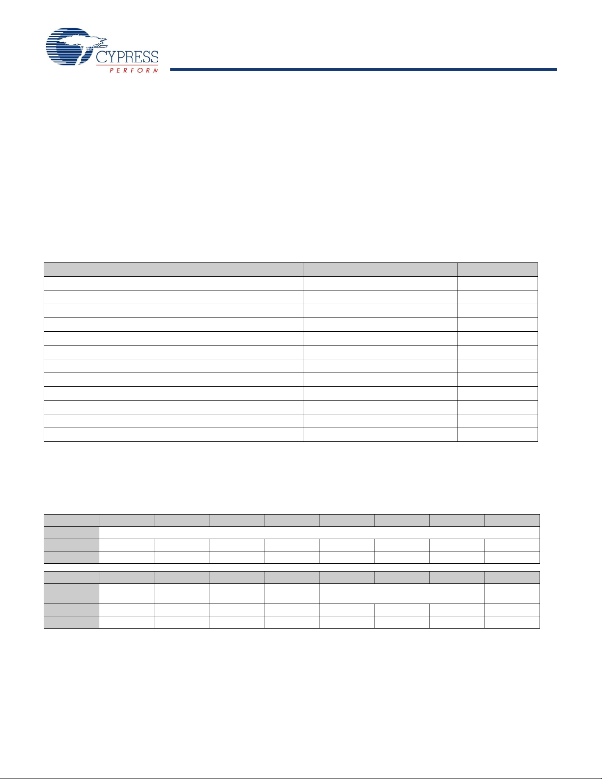
CY7C67300
Port A SOF/EOP Enable (Bit 0)
The Port A SOF/EOP Enable bit is only applicable in host mode.
Reserved
Write all reserved bits with ’0’.
In device mode this bit must be written as ‘0’. In host mode this
bit enables or disables SOFs or EOPs for Port A. Either SOFs or
EOPs are generated depending on the LOA bit in the USB n
Control register when Port A is active.
1: Enable SOFs or EOPs
0: Disable SOFs or EOPs
USB Host Only Registers
There are twelve sets of dedicated registers for USB host only operation. Each set consists of two identical registers (unless otherwise
noted), one for Host Port 1 and one for Host Port 2. These register sets are covered in this section and summarized in Table 47.
Table 47. USB Host Only Register
Register Name Address (Host 1/Host 2) R/W
Host n Control Register 0xC080/0xC0A0 R/W
Host n Address Register 0xC082/0xC0A2 R/W
Host n Count Register 0xC084/0xC0A4 R/W
Host n Endpoint Status Register 0xC086/0xC0A6 R
Host n PID Register 0xC086/0xC0A6 W
Host n Count Result Register 0xC088/0xC0A8 R
Host n Device Address Register 0xC088/0xC0A8 W
Host n Interrupt Enable Register 0xC08C/0xC0AC R/W
Host n Status Register 0xC090/0xC0B0 R/W
Host n SOF/EOP Count Register 0xC092/0xC0B2 R/W
Host n SOF/EOP Counter Register 0xC094/0xC0B4 R
Host n Frame Register 0xC096/0xC0B6 R
Host n Control Register [R/W]
■ Host 1 Control Register 0xC080
■ Host 2 Control Register 0xC0A0
Table 48. Host n Control Register
Bit # 15 14 13 12 11 10 9 8
Field Reserved
Read/Write - - - - - - - Default 0 0 0 0 0 0 0 0
Bit # 7 6 5 4 3 2 1 0
Field
Read/Write R/W R/W R/W R/W - - - R/W
Default 0 0 0 0 0 0 0 0
Preamble
Enable
Register Description
The Host n Control register allows high level USB transaction
control.
Sequence
Select
Sync
Enable
ISO
Enable
Reserved Arm
Enable
Preamble Enable (Bit 7)
The Preamble Enable bit enables or disables the transmission of
a preamble packet before all low-speed packets. Set this bit only
when communicating with a low-speed device.
1: Enable Preamble packet
0: Disable Preamble packet
Document #: 38-08015 Rev. *J Page 29 of 99
[+] Feedback
Page 30
CY7C67300
Sequence Select (Bit 6)
The Sequence Select bit sets the data toggle for the next packet.
This bit has no effect on receiving data packets; sequence
checking must be handled in firmware.
1: Send DATA1
ISO Enable (Bit 4)
The ISO Enable bit enables or disables an isochronous trans-
action.
1: Enable isochronous transaction
0: Disable isochronous transaction
0: Send DATA0
Arm Enable (Bit 0)
Sync Enable (Bit 5)
The Sync Enable bit synchronizes the transfer with the SOF
packet in full-speed mode and the EOP packet in low-speed
mode.
1: The next enabled packet is transferred after the SOF or EOP
packet is transmitted
0: The next enabled packet is transferred as soon as the SIE is
free
The Arm Enable bit arms an endpoint and starts a transaction.
This bit is automatically cleared to ‘0’ when a transaction is
complete.
1: Arm endpoint and begin transaction
0: Endpoint disarmed
Reserved
Write all reserved bits with ’0’.
Host n Address Register [R/W]
■ Host 1 Address Register 0xC082
■ Host 2 Address Register 0xC0A2
Table 49. Host n Address Register
Bit # 15 14 13 12 11 10 9 8
Field Address...
Read/Write R/W R/W R/W R/W R/W R/W R/W R/W
Default 0 0 0 0 0 0 0 0
Bit # 7 6 5 4 3 2 1 0
Field ...Address
Read/Write R/W R/W R/W R/W R/W R/W R/W R/W
Default 0 0 0 0 0 0 0 0
Register Description
The Host n Address register is used as the base pointer into
memory space for the current host tran sa ctions.
Address (Bits [15:0])
The Address field sets the address pointer into internal RAM or
ROM.
Host n Count Register [R/W]
■ Host 1 Count Register 0xC084.
■ Host 2 Count Register 0xC0A4.
Table 50. Host n Count Register
Bit # 15 14 13 12 11 10 9 8
Field
Read/Write - R/W - - - - R/W R/W
Default 0 0 0 0 0 0 0 0
Bit # 7 6 5 4 3 2 1 0
Field ...Count
Read/Write R/W R/W R/W R/W R/W R/W R/W R/W
Default 0 0 0 0 0 0 0 0
Reserved Port
Select
Reserved Count...
Document #: 38-08015 Rev. *J Page 30 of 99
[+] Feedback
Page 31

CY7C67300
Register Description
The Host n Count register is used to hold the number of bytes
(packet length) for the current transaction. The maximum packet
length is 1023 bytes in ISO mode. The Host Count value is used
to determine how many bytes to transmit, or the maximum
number of bytes to receive. If the number of received bytes is
Table 51. Port Select Definition
Port Select
Host/Device 1
Active Port
0AA
1BB
Host/Device 2
Active Port
greater then the Host Count value then an overflow condition is
flagged by the Overflow bit in the Host n Endpoint Status register.
Port Select (Bit 14)
The Port Select bit selects which of the two active ports is
selected and is summarized in Table 51.
1: Port 1B or Port 2B is enabled
0: Port 1A or Port 2A is enabled
Count (Bits [9:0])
The Count field sets the value for the current transaction data
packet length. This value is retained when switching between
host and device mode, and back again.
Reserved
Write all reserved bits with ’0’.
Host n Endpoint Status Register [R]
■ Host 1 Endpoint Status Register 0xC086
■ Host 2 Endpoint St atu s Re giste r 0xC 0 A6
Table 52. Host n Endpoint Status Register
Bit # 15 14 13 12 11 10 9 8
Field
Read/Write - - - - R R - Default 0 0 0 0 0 0 0 0
Reserved Overflow
Flag
Underflow
Flag
Reserved
Bit # 7 6 5 4 3 2 1 0
Stall
Field
Read/Write R R R - R R R R
Default 0 0 0 0 0 0 0 0
Flag
Register Description
The Host n Endpoint Status register is a read only register that
provides status for the last USB transaction.
Overflow Flag (Bit 11)
The Overflow Flag bit indicates that the received data in the last
data transaction exceeded the maximum length specified in the
Host n Count register. The Overflow Flag must be checked in
response to a Length Exception signified by the Length
Exception Flag set to ‘1’.
1: Overflow condition occurred
0: Overflow condition did not occur
Underflow Flag (Bit 10)
The Underflow Flag bit indicates that the received data in the last
data transaction was less than the maximum length specified in
the Host n Count register. The Underflow Flag must be checked
in response to a Length Exception signified by the Length
Exception Flag set to ‘1’.
1: Underflow condition occurred
0: Underflow condition did not occur
NAK
Flag
Length
Exception
Flag
Reserved Sequence
Status
Stall Flag (Bit 7)
The Stall Flag bit indicates that the peripheral device replied with
a Stall in the last tran sa ction.
1: Device returned Stall
0: Device did not return Stall
NAK Flag (Bit 6)
The NAK Flag bit indicates that the peripheral device replied with
a NAK in the last transaction.
1: Device returned NAK
0: Device did not return NAK
Length Exception Flag (Bit 5)
The Length Exception Flag bit indicates that the received data in
the data stage of the last transaction does not equal the
maximum Host Count specified in the Host n C ount register. A
Length Exception can either mean an overflow or underflow and
the Overflow and Underflow flags (bits 11 and 10, respectively)
must be checked to determine which event occurred.
1: An overflow or underflow condition occurred
0: An overflow or underflow condition did not occur
Timeout
Flag
Error
Flag
ACK
Flag
Document #: 38-08015 Rev. *J Page 31 of 99
[+] Feedback
Page 32

CY7C67300
Sequence Status (Bit 3)
The Sequence Status bit indicates the state of the last received
data toggle from the device. Firmware is responsible for
monitoring and handling the sequence status. The Sequence bit
is only valid if the ACK bit is set to ‘1’. The Sequence bit is set to
a STALL. Overflow and Underflow are not considered errors and
do not affect this bit. CRC5 and CRC16 errors result in an Error
flag along with receiving incorrect packet types.
1: Error detected
0: No error detected
‘0’ when an error is detected in the transa ctio n a nd t he Error b it
is set.
1: DATA1
0: DATA0
Timeout Flag (Bit 2)
The Timeout Flag bit indicates if a timeout condition occurred for
the last transaction. A timeout condition can occur when a device
either takes too long to respond to a USB host request or takes
too long to respond with a handshake.
1: Timeout occurred
0: Timeout did not occur
ACK Flag (Bit 0)
The ACK Flag bit indicates two different conditions depending on
the transfer type. For non-isochronous transfers, this bit repre-
sents a transaction ending by receiving or sending an ACK
packet. For isochronous transfers, this bit represents a
successful transaction that is not represented by an ACK packet.
1: For non-isochronous transfers, the transaction was ACKed.
For isochronous transfers, the transaction was completed
successfully
0: For non-isochronous transfers, the transaction was not
ACKed. For isochronous transfers, the transaction did not
complete successfully
Error Flag (Bit 1)
The Error Flag bit indicates a transaction failed for any re ason
other than the following: timeout, receiving a NAK, or recei ving
Host n PID Register [W]
■ Host 1 PID Register 0xC086
■ Host 2 PID Register 0xC0A6
Table 53. Host n PID Register
Bit # 15 14 13 12 11 10 9 8
Field Reserved
Read/Write - - - - - - - Default 0 0 0 0 0 0 0 0
Bit # 7 6 5 4 3 2 1 0
Field PID Select Endpoint Select
Read/Write W W W W W W W W
Default 0 0 0 0 0 0 0 0
Document #: 38-08015 Rev. *J Page 32 of 99
[+] Feedback
Page 33

CY7C67300
Register Description
The Host n PID register is a write only register that provides the
PID and Endpoint information to the USB SIE to be used in the
Endpoint Select (Bits [3:0])
The Endpoint field allows addressing of up to 16 different
endpoints.
next transaction.
Reserved
PID Select (Bits [7:4])
Write all reserved bits with ’0’.
The PID Select field is defined in T able54. ACK and NAK tokens
are automatically sent based on settings in the Host n Control
register and do not need to be written in this register.
Table 54. PID Select Definition
PID TYPE PID Select [7:4]
SETUP 1101 (D Hex)
IN 1001 (9 Hex)
OUT 0001 (1 Hex)
SOF 0101 (5 Hex)
PREAMBLE 1100 (C Hex)
NAK 1010 (A Hex)
STALL 1110 (E Hex)
DATA0 0011 (3 Hex)
DATA1 1011 (B Hex)
Host n Count Result Register [R]
■ Host 1 Count Result Register 0xC088
■ Host 2 Count Result Register 0xC0A8
Table 55. Host n Count Result Register
Bit # 15 14 13 12 11 10 9 8
Field Result...
Read/Write R R R R R R R R
Default 0 0 0 0 0 0 0 0
Bit # 7 6 5 4 3 2 1 0
Field ...Result
Read/Write R R R R R R R R
Default 0 0 0 0 0 0 0 0
Register Description
The Host n Count Result register is a read only register that
contains the size difference in bytes between the Host Count
Value specified in the Host n Count register and the last packet
received. If an overflow or underflow condition occurs, that is the
received packet length differs from the value specified in the Host
n Count register, the Length Exception Flag bit in the Host n
Endpoint Status register is set. The value in this register is only
value when the Length Exception Flag bit is set and the Error
Flag bit is not set, both bits are in the Host n Endpoint Status
register.
Result (Bits [15:0])
The Result field contains the differences in bytes between the
received packet and the value specified in the Host n Count
register. If an overflow condition occurs, Result [15:10] is set to
‘ 111111 ’, a 2 ’ s co m p l e me n t v a l u e i n d i c a t in g t h e a dd i t i o n a l b y t e
count of the received packet. If an underflow condition occurs,
Result [15:0] indicates the excess bytes count (number of bytes
not used).
Reserved
Write all reserved bits with ’0’.
Document #: 38-08015 Rev. *J Page 33 of 99
[+] Feedback
Page 34

CY7C67300
Host n Device Address Register [W]
■ Host 1 Device Address Register 0xC088
■ Host 2 Device Address Register 0xC0A8
Table 56. Host n Device Address Register
Bit # 15 14 13 12 11 10 9 8
Field Reserved...
Read/Write - - - - - - - Default 0 0 0 0 0 0 0 0
Bit # 7 6 5 4 3 2 1 0
Field ...Reserved Address
Read/Write - W W W W W W W
Default 0 0 0 0 0 0 0 0
Register Description
The Host n Device Address register is a write only register that
contains the USB Device Address that the host wants to communicate with.
Address (Bits [6:0])
The Address field contains the value of the USB address for the
next device that the host is going to communicate with. This
value must be written by firmware.
Reserved
Write all reserved bits with ’0’.
Host n Interrupt Enable Register [R/W]
■ Host 1 Interrupt Enable Register 0xC08C
■ Host 2 Interrupt Enable Register 0xC0AC
Table 57. Host n Interrupt Enable Register
Bit # 15 14 13 12 11 10 9 8
VBUS
Field
Read/Write R/W R/W - - - - R/W -
Default 0 0 0 0 0 0 0 0
Bit # 7 6 5 4 3 2 1 0
Field
Read/Write R/W R/W R/W R/W - - - R/W
Default 0 0 0 0 0 0 0 0
Interrupt
Enable
Port B
Wake Interrupt
Enable
ID Interrupt
Enable
Port A
Wake Interrupt
Enable
Port B Connect
Change
Interrupt
Enable
Reserved SOF/EOP
Port A Connect
Change
Interrupt
Enable
Interrupt
Enable
Reserved Done
Reserved
Interrupt
Enable
Register Description
The Host n Interrupt Enable register enables control over host
related interrupts.
In this register a bit set to ‘1’ enables the corresponding interrupt
while ‘0’ disables the interrupt.
VBUS Interrupt Enable (Bit 15)
The VBUS Interrupt Enable bit enables or disables the OTG
VBUS interrupt. When enabled this interrupt triggers on both the
rising and falling edge of VBUS at the 4.4V status (only
supported in Port 1A). This bit is only available for Host 1 and is
1: Enable VBUS interrupt
0: Disable VBUS interrupt
ID Interrupt Enable (Bit 14)
The ID Interrupt Enable bit enables or disables the OTG ID
interrupt. When enabled this interrupt triggers on both the rising
and falling edge of the OTG ID pin (only supported in Port 1A).
This bit is only available for Host 1 and is a reserved bit in Host 2.
1: Enable ID interrupt
0: Disable ID interrupt
a reserved bit in Host 2.
Document #: 38-08015 Rev. *J Page 34 of 99
[+] Feedback
Page 35

CY7C67300
SOF/EOP Interrupt Enable (Bit 9)
The SOF/EOP Interrupt Enable bit enables or disables the
SOF/EOP timer interrupt
1: Enable SOF/EOP timer interrupt
0: Disable SOF/EOP timer interrupt
Port B Wake Interrupt Enable (Bit 7)
The Port B Wake Interrupt Enable bit enables or disables the
remote wakeup interrupt for Port B
1: Enable remote wakeup interrupt for Port B
0: Disable remote wakeup interrupt for Port B
Port A Wake Interrupt Enable (Bit 6)
The Port A Wake Interrupt Enable bit enables or disables the
remote wakeup interrupt for Port A
1: Enable remote wakeup interrupt for Port A
0: Disable remote wakeup interrupt for Port A
Port B Connect Change Interrupt Enable (Bit 5)
The Port B Connect Change Interrupt Enable bit enables or
disables the Port B Connect Change interrupt on Port B. Thi s
1: Enable Connect Change interrupt
0: Disable Connect Change interrupt
Port A Connect Change Interrupt Enable (Bit 4)
The Port A Connect Change Interrupt Enable bit enables or
disables the Connect Change interrupt on Port A. This inte rrupt
triggers when either a device is inserted (SE0 state to J state) or
a device is removed (J state to SE0 state).
1: Enable Connect Change interrupt
0: Disable Connect Change interrupt
Done Interrupt Enable (Bit 0)
The Done Interrupt Enable bit enables or disables the USB
Transfer Done interrupt. The USB Transfer Done triggers when
either the host responds with an ACK, or a device responds with
any of the following: ACK, NAK, STALL, or Timeout. This
interrupt is used for both Port A and Port B.
1: Enable USB Transfer Done interrupt
0: Disable USB Transfer Done interrupt
Reserved
Write all reserved bits with ’0’.
interrupt triggers when either a device is inserted (SE0 state to J
state) or a device is removed (J state to SE0 state).
Host n Status Register [R/W]
■ Host 1 Status Register 0xC090
■ Host 2 Status Register 0xC0B0
Table 58. Host n Status Register
Bit # 15 14 13 12 11 10 9 8
Field
Read/Write R/W R/W - - - - R/W -
Default X X X X X X X X
VBUS Interrupt
Flag
ID Interrupt
Flag
Reserved SOF/EOP
Interrupt Flag
Reserved
Bit # 7 6 5 4 3 2 1 0
Port B
Field
Read/Write R/W R/W R/W R/W R/W R/W - R/W
Default X X X X X X X X
Wake Interrupt
Flag
Register Description
The Host n Status register provides status information for host
operation. Pending interrupts can be cleared by writing a ‘ 1’ to
the corresponding bit. This register can be accessed by the HPI
interface.
VBUS Interrupt Flag (Bit 15)
The VBUS Interrupt Flag bit indicates the status of the OTG
VBUS interrupt (only for Port 1A). When enabled this interrupt
triggers on both the rising and falling edge of VBUS at 4.4V. This
bit is only available for Host 1 and is a reserved bit in Host 2.
Port A
Wake Interrupt
Flag
Port B Connect
Change
Interrupt Flag
Port A Connect
Change Interrupt
Flag
Port B
SE0
Status
Port A
SE0
Status
Reserved Done Interrupt
1: Interrupt triggered
0: Interrupt did not trigger
ID Interrupt Flag (Bit 14)
The ID Interrupt Flag bit indicates the status of the OTG ID
interrupt (only for Port 1A). When enabled this interrupt triggers
on both the rising and falling edge of the OTG ID pin. This bi t i s
only available for Host 1 and is a reserved bit in Host 2.
1: Interrupt triggered
0: Interrupt did not trigger
Flag
Document #: 38-08015 Rev. *J Page 35 of 99
[+] Feedback
Page 36

CY7C67300
SOF/EOP Interrupt Flag (Bit 9)
The SOF/EOP Interrupt Flag bit indicates the status of the
SOF/EOP Timer interrupt. This bit triggers ‘1’ when the
SOF/EOP timer expires.
1: Interrupt triggered
0: Interrupt did not trigger
Port B Wake Interrupt Flag (Bit 7)
The Port B Wake Interrupt Flag bit indicates remote wakeup on
PortB.
1: Interrupt triggered
0: Interrupt did not trigger
Port A Wake Interrupt Flag (Bit 6)
The Port A Wake Interrupt Flag bit indicates remote wakeup on
PortA.
1: Interrupt triggered
0: Interrupt did not trigger
Port B Connect Change Interrupt Flag (Bit 5)
The Port B Connect Change Interrupt Flag bit indicates the
status of the Connect Change interrupt on Port B. This bit
triggers ‘1’ on either a rising edge or falling edge of a USB Reset
condition (device inserted or removed). Together with the Port B
SE0 Status bit, it can be determined whether a device was
inserted or removed.
1: Interrupt triggered
0: Interrupt did not trigger
Port A Connect Change Interrupt Flag (Bit 4)
The Port A Connect Change Interrupt Flag bit indicates the
status of the Connect Change interrupt on Port A. This bit
triggers ‘1’ on either a rising edge or falling edge of a USB Reset
condition (device inserted or removed). Together with the Port A
SE0 Status bit, it can be determined whether a device was
inserted or removed.
1: Interrupt triggered
0: Interrupt did not trigger
Port B SE0 Status (Bit 3)
The Port B SE0 Status bit indicates if Port B is in a SE0 state or
not. Together with the Port B Connect Change Interrupt Flag bit,
it can be determined whether a device was inserted (non-SE0
condition) or removed (SE0 condition).
1: SE0 condition
0: Non-SE0 condition
Port A SE0 Status (Bit 2)
The Port A SE0 Status bit indicates if Port A is in a SE0 state or
not. Together with the Port A Connect change Interrupt Flag bit,
it can be determined whether a device was inserted (non-SE0
condition) or removed (SE0 condition).
1: SE0 condition
0: Non-SE0 condition
Done Interrupt Flag (Bit 0)
The Done Interrupt Flag bit indicates the status of the USB
Transfer Done interrupt. The USB Transfer Done triggers when
either the host responds with an ACK, or a device responds with
any of the following: ACK, NAK, STALL, or Timeout. This
interrupt is used for both Port A and Port B.
1: Interrupt triggered
0: Interrupt did not trigger
Host n SOF/EOP Count Register [R/W]
■ Host 1 SOF/EOP Count Register 0xC092
■ Host 2 SOF/EOP Count Register 0xC0B2
Table 59. Host n SOF/EOP Count Register
Bit # 15 14 13 12 11 10 9 8
Field Reserved Count...
Read/Write - - R/W R/W R/W R/W R/W R/W
Default 0 0 1 0 1 1 1 0
Bit # 7 6 5 4 3 2 1 0
Field ...Count
Read/Write R/W R/W R/W R/W R/W R/W R/W R/W
Default 1 1 1 0 0 0 0 0
Register Description
The Host n SOF/EOP Count register contains the SOF/EOP
Count Value that is loaded into the SOF/EOP counter. This value
is loaded each time the SOF/EOP counter counts down to zero.
The default value set in this register at power up is 0x2EE0 which
generates a 1 ms time frame. The SOF/EOP counter i s a d own
counter decremented at a 12 MHz rate. When this register is
read, the value returned is the programmed SOF/EOP count
value.
Count (Bits [13:0])
The Count field sets the SOF/EOP counter duration.
Reserved
Write all reserved bits with ’0’.
Document #: 38-08015 Rev. *J Page 36 of 99
[+] Feedback
Page 37

CY7C67300
Host n SOF/EOP Counter Register [R]
■ Host 1 SOF/EOP Counter Register 0xC094
■ Host 2 SOF/EOP Counter Register 0xC0B4
Table 60. Host n SOF/EOP Counter Register
Bit # 15 14 13 12 11 10 9 8
Field Reserved Counter...
Read/Write - - R R R R R R
Default X X X X X X X X
Bit # 7 6 5 4 3 2 1 0
Field ...Counter
Read/Write R R R R R R R R
Default X X X X X X X X
Register Description
The Host n SOF/EOP Counter register contains the current value
of the SOF/EOP down counter. This value can be used to
Counter (Bits [13:0])
The Counter field contains the current value of the SOF/EOP
down counter.
determine the time remaining in the current frame.
Host n Frame Register [R]
■ Host 1 Frame Register 0xC096
■ Host 2 Frame Register 0xC0B6
Table 61. Host n Frame Register
Bit # 15 14 13 12 11 10 9 8
Field Reserved Frame...
Read/Write - - - - - R R R
Default 0 0 0 0 0 0 0 0
Bit # 7 6 5 4 3 2 1 0
Field ...Frame
Read/Write R R R R R R R R
Default 0 0 0 0 0 0 0 0
Register Description
The Host n Frame register maintains the next frame number to
be transmitted (current frame number + 1). This value is updated
Frame (Bits [10:0])
The Frame field contains the next frame number to be trans-
mitted.
after each SOF transmission. This register resets to 0x0000 after
each CPU write to the Host n SOF/EOP Count register (Host 1:
0xC092 Host 2: 0xC0B2).
Reserved
Write all reserved bits with ’0’.
Document #: 38-08015 Rev. *J Page 37 of 99
[+] Feedback
Page 38

CY7C67300
USB Device Only Registers
There are eleven sets of USB Device Only registers. All sets consist of at least two registers, one for Device Port 1 and one for Device
Port 2. In addition, each Device port has eight possible endpoints. This gives each endpoint register set eight registers for each Device
Port for a total of sixteen registers per set. The USB Device Only registers are covered in this section and summarized in Table 62.
Table 62. USB Device Only Registers
Register Name Address (Device 1/Device 2) R/W
Device n Endpoint n Control Register 0x02n0 R/W
Device n Endpoint n Address Register 0x02n2 R/W
Device n Endpoint n Count Register 0x02n4 R/W
Device n Endpoint n Status Register 0x02n6 R/W
Device n Endpoint n Count Result Register 0x02n8 R/W
Device n Port Select Register 0xC084/0xC0A4 R/W
Device n Interrupt Enable Register 0xC08C/0xC0AC R/W
Device n Address Register 0xC08E/0xC0AE R/W
Device n Status Register 0xC090/0xCB0 R/W
Device n Frame Number Register 0xC092/0xC0B2 R
Device n SOF/EOP Count Register 0xC094/0xC0B4 W
Device n Endpoint n Control Register [R/W]
■ Device n Endpoint 0 Control Register [Device 1: 0x0200 Device 2: 0x0280]
■ Device n Endpoint 1 Control Register [Device 1: 0x0210 Device 2: 0x0290]
■ Device n Endpoint 2 Control Register [Device 1: 0x0220 Device 2: 0x02A0]
■ Device n Endpoint 3 Control Register [Device 1: 0x0230 Device 2: 0x02B0]
■ Device n Endpoint 4 Control Register [Device 1: 0x0240 Device 2: 0x02C0]
■ Device n Endpoint 5 Control Register [Device 1: 0x0250 Device 2: 0x02D0]
■ Device n Endpoint 6 Control Register [Device 1: 0x0260 Device 2: 0x02E0]
■ Device n Endpoint 7 Control Register [Device 1: 0x0270 Device 2: 0x02F0]
Table 63. Device n Endpoint n Control Register
Bit # 15 14 13 12 11 10 9 8
Field Reserved
Read/Write - - - - - - - Default X X X X X X X X
Bit # 7 6 5 4 3 2 1 0
IN/OUT
Field
Read/Write R/W R/W R/W R/W R/W R/W R/W R/W
Default X X X X X X X X
Ignore
Enable
Register Description
The Device n Endpoint n Contro l register provides contro l over a
single EP in device mode. There are a total of eight endpoints for
each of the two ports. All endpoints have the same definition for
their Device n Endpoint n Control register.
Sequence
Select
Stall
Enable
ISO
Enable
NAK
Interrupt
Enable
Direction
Select
Enable Arm
Enable
IN/OUT Ignore Enable (Bit 7)
The IN/OUT Ignore Enable bit forces endpoint 0 (EP0) to ignore
all IN and OUT requests. Set this bit so that EP0 onl y accepts
Setup packets at the start of each transfer. Clear this bit to accept
IN/OUT transactions. This bit only applies to EP0.
1: Ignore IN/OUT requests
0: Do not ignore IN/OUT requests
Document #: 38-08015 Rev. *J Page 38 of 99
[+] Feedback
Page 39

CY7C67300
Sequence Select (Bit 6)
The Sequence Select bit determines whether a DATA0 or a
DATA1 is sent for the next data toggle. This bit has no effect on
receiving data packets; sequence checking must be handled in
firmware.
1: Send a DATA1
0: Send a DATA0
Stall Enable (Bit 5)
The Stall Enable bit sends a St all in response to the next request
(unless it is a setup request, which are always ACKed). This is a
sticky bit and continues to respond with Stalls until cleared by
firmware.
1: Send Stall
0: Do not send Stall
ISO Enable (Bit 4)
The ISO Enable bit enables and disables an isochronous transaction. This bit is only valid for EPs 1–7 and has no function for
EP0.
1: Enable isochronous transaction
0: Disable isochronous transaction
NAK Interrupt Enable (Bit 3)
The NAK Interrupt Enable bit enables and disables t he generation of an Endpoint n interrupt when the device responds to the
host with a NAK. The Endpoint n Interrupt Enable bit in the
Device n Interrupt Enable register must also be set. W hen a NAK
is sent to the host, the corresponding EP Interrupt Flag in the
Device n Status register is set. In addition, the NAK Flag in the
Device n Endpoint n Status register is set.
1: Enable NAK interrupt
0: Disable NAK interrupt
Direction Select (Bit 2)
The Direction Select bit needs to be set according to the
expected direction of the next data stage in the next transaction.
If the data stage direction is different from what is set in this bit,
it gets NAKed and either the IN Exception Flag or the OUT
Exception Flag is set in the Device n Endpoint n Status register.
If a setup packet is received and the Direction Select bit is set
incorrectly, the setup is ACKed and the Setup Status Flag is set
(refer to the setup bit of the Device n Endpoint n Status Register
[R/W] on page 41 for details).
1: OUT transfer (host to device)
0: IN transfer (device to host)
Enable (Bit 1)
Set the Enable bit to allow transfers to the endpoint. If Enable is
set to ‘0’ then all USB traffic to this endpoint is ignored. If Enable
is set ‘1’ and Arm Enable (bit 0) is set ‘0’ then NAKs are automat-
ically returned from this endpoint (except setup packets which
are always ACKed as long as the Enable bit is set).
1: Enable transfers to an endpoint
0: Do not allow transfers to an endp oin t
Arm Enable (Bit 0)
The Arm Enable bit arms the endpoint to transfer or receive a
packet. This bit is cleared to ‘0’ when a transaction is complete.
1: Arm endpoint
0: Endpoint disarmed
Reserved
Write all reserved bits with ’0’.
Device n Endpoint n Address Register [R/W]
■ Device n Endpoint 0 Address Register [Device 1: 0x0202 Device 2: 0x0282]
■ Device n Endpoint 1 Address Register [Device 1: 0x0212 Device 2: 0x0292]
■ Device n Endpoint 2 Address Register [Device 1: 0x0222 Device 2: 0x02A2]
■ Device n Endpoint 3 Address Register [Device 1: 0x0232 Device 2: 0x02B2]
■ Device n Endpoint 4 Address Register [Device 1: 0x0242 Device 2: 0x02C2]
■ Device n Endpoint 5 Address Register [Device 1: 0x0252 Device 2: 0x02D2]
■ Device n Endpoint 6 Address Register [Device 1: 0x0262 Device 2: 0x02E2]
■ Device n Endpoint 7 Address Register [Device 1: 0x0272 Device 2: 0x02F2]
Table 64. Device n Endpoint n Address Register
Bit # 15 14 13 12 11 10 9 8
Field Address...
Read/Write R/W R/W R/W R/W R/W R/W R/W R/W
Default X X X X X X X X
Bit # 7 6 5 4 3 2 1 0
Field ...Address
Read/Write R/W R/W R/W R/W R/W R/W R/W R/W
Default X X X X X X X X
Document #: 38-08015 Rev. *J Page 39 of 99
[+] Feedback
Page 40

CY7C67300
Register Description
The Device n Endpoint n Address register is used as the base
pointer into memory space for the current Endpoint transaction.
Address (Bits [15:0])
The Address field sets the base address for the current trans-
action on a signal endpoint.
There are a total of eight endpoints for each of the two ports. All
endpoints have the same definition for their Device n Endpoint n
Address register.
Device n Endpoint n Count Register [R/W]
■ Device n Endpoint 0 Count Register [Device 1: 0x0204 Device 2: 0x0284]
■ Device n Endpoint 1 Count Register [Device 1: 0x0214 Device 2: 0x0294]
■ Device n Endpoint 2 Count Register [Device 1: 0x0224 Device 2: 0x02A4]
■ Device n Endpoint 3 Count Register [Device 1: 0x0234 Device 2: 0x02B4]
■ Device n Endpoint 4 Count Register [Device 1: 0x0244 Device 2: 0x02C4]
■ Device n Endpoint 5 Count Register [Device 1: 0x0254 Device 2: 0x02D4]
■ Device n Endpoint 6 Count Register [Device 1: 0x0264 Device 2: 0x02E4]
■ Device n Endpoint 7 Count Register [Device 1: 0x0274 Device 2: 0x02F4]
Table 65. Device n Endpoint n Count Register
Bit # 15 14 13 12 11 10 9 8
Field Reserved Count...
Read/Write - - - - - - R/W R/W
Default X X X X X X X X
Bit # 7 6 5 4 3 2 1 0
Field ...Count
Read/Write R/W R/W R/W R/W R/W R/W R/W R/W
Default X X X X X X X X
Register Description
The Device n Endpoint n Count register designates the
maximum packet size that can be received from the host for OUT
Count (Bits [9:0])
The Count field sets the current transaction packet length for a
single endpoint.
transfers for a single endpoint. This register also designates the
packet size to be sent to the host in response to the next IN token
for a single endpoint. The maximum packet length is 1023 bytes
in ISO mode. There are a total of eight endpoints for each of the
Reserved
Write all reserved bits with ’0’.
two ports. All endpoint s have the same d efinition for their Device
n Endpoint n Count register.
Document #: 38-08015 Rev. *J Page 40 of 99
[+] Feedback
Page 41

CY7C67300
Device n Endpoint n Status Register [R/W]
■ Device n Endpoint 0 Status Register [Device 1: 0x0206 Device 2: 0x0286]
■ Device n Endpoint 1 Status Register [Device 1: 0x0216 Device 2: 0x0296]
■ Device n Endpoint 2 Status Register [Device 1: 0x0226 Device 2: 0x02A6]
■ Device n Endpoint 3 Status Register [Device 1: 0x0236 Device 2: 0x02B6]
■ Device n Endpoint 4 Status Register [Device 1: 0x0246 Device 2: 0x02C6]
■ Device n Endpoint 5 Status Register [Device 1: 0x0256 Device 2: 0x02D6]
■ Device n Endpoint 6 Status Register [Device 1: 0x0266 Device 2: 0x02E6]
■ Device n Endpoint 7 Status Register [Device 1: 0x0276 Device 2: 0x02F6]
Table 66. Device n Endpoint n Status Register
Bit # 15 14 13 12 11 10 9 8
Field
Read/Write - - - - R/W R/W R/W R/W
Default X X X X X X X X
Bit # 7 6 5 4 3 2 1 0
Field
Read/Write R/W R/W R/W R/W R/W R/W R/W R/W
Default X X X X X X X X
Stall
Flag
Reserved Overflow
NAK
Flag
Length
Exception Flag
Setup
Flag
Flag
Sequence
Flag
Underflow
Flag
Timeout
Flag
OUT
Exception FlagINException Flag
Error
Flag
ACK
Flag
Register Description
The Device n Endpoint n Status register provides packet status
information for the last transaction received or transmitted. This
register is updated in hardware and does not need to be cleared
by firmware. There are a total of eight endpoints for each of the
two ports. All endpoint s have the same d efinition for their Device
n Endpoint n Status register.
The Device n Endpoint n Status register is a memory based
register that must be initialized to 0x0000 before USB Device
operations are initiated. After initialization, do not write to thi s
register again.
Overflow Flag (Bit 11)
The Overflow Flag bit indicates that the received data in the last
data transaction exceeded the maximum length specified in the
Device n Endpoint n Count register. The Overflow Flag must be
checked in response to a Length Exception signified by the
Length Exception Flag set to ‘1’.
1: Overflow condition occurred
0: Overflow condition did not occur
Underflow Flag (Bit 10)
The Underflow Flag bit indicates that the received data in the last
data transaction was less then the maximum length specified in
the Device n Endpoint n Count register. The Underflow Flag must
be checked in response to a Length Exception signified by the
Length Exception Flag set to ‘1’.
1: Underflow condition occurred
0: Underflow condition did not occur
OUT Exception Flag (Bit 9)
The OUT Exception Flag bit indicates when the device received
an OUT packet when armed for an IN.
1: Received OUT when armed for IN
0: Received IN when armed for IN
IN Exception Flag (Bit 8)
The IN Exception Flag bit indicates when the device rece ived an
IN packet when armed for an OUT.
1: Received IN when armed for OUT
0: Received OUT when armed for OUT
Stall Flag (Bit 7)
The Stall Flag bit indicates that a Stall packet was sent to the
host.
1: Stall packet was sent to the host
0: Stall packet was not sent
NAK Flag (Bit 6)
The NAK Flag bit indicates that a NAK packet was sent to the
host.
1: NAK packet was sent to the host
0: NAK packet was not sent
Length Exception Flag (Bit 5)
The Length Exception Flag bit indicates the received data in the
data stage of the last transaction does not equal the maximum
Endpoint Count specified in the Device n Endpoint n Count
register. A Length Exception can either mean an overflow or
Document #: 38-08015 Rev. *J Page 41 of 99
[+] Feedback
Page 42

CY7C67300
underflow and the Overflow and Underflow flags (bits 11 and 10
respectively) must be checked to determine which event
occurred.
1: An overflow or underflow condition occurred
0: An overflow or underflow condition did not occur
Setup Flag (Bit 4)
The Setup Flag bit indicates that a setup packet was received.
In device mode setup packets are stored at memory location
Timeout Flag (Bit 2)
The Timeout Flag bit indicates whether a timeout condition
occurred on the last transaction. On t he device side, a timeout
can occur if the device sends a data packet in response to an IN
request but then does not receive a handshake packet in a
predetermined time. It can also occur if the device does not
receive the data stage of an OUT transfer in time.
1: Timeout occurred
0: Timeout condition did not occur
0x0300 for Device 1 and 0x0308 for Device 2. Setup packets are
always accepted regardless of the Direction Select and Arm
Enable bit settings as long as the Device n EP n Control register
Enable bit is set.
1: Setup packet was received
0: Setup packet was not received
Sequence Flag (Bit 3)
The Sequence Flag bit indicates whether the last data toggle
received was a DATA1 or a DATA0. This bit has no effect on
receiving data packets; sequence checking must be handled in
firmware.
1: DATA1 was received
0: DATA0 was received
Error Flag (Bit 2)
The Error Flag bit is set if a CRC5 and CRC16 error occurs, or if
an incorrect packet type is received. Overflow and underflow are
not considered errors and do not affect this bit.
1: Error occurred
0: Error did not occur
ACK Flag (Bit 0)
The ACK Flag bit indicates whether the last transaction was
ACKed.
1: ACK occurred
0: ACK did not occur
Device n Endpoint n Count Result Register [R/W]
■ Device n Endpoint 0 Count Result Register [Device 1: 0x0208 Device 2: 0x0288]
■ Device n Endpoint 1 Count Result Register [Device 1: 0x0218 Device 2: 0x0298]
■ Device n Endpoint 2 Count Result Register [Device 1: 0x0228 Device 2: 0x02A8]
■ Device n Endpoint 3 Count Result Register [Device 1: 0x0238 Device 2: 0x02B8]
■ Device n Endpoint 4 Count Result Register [Device 1: 0x0248 Device 2: 0x02C8]
■ Device n Endpoint 5 Count Result Register [Device 1: 0x0258 Device 2: 0x02D8]
■ Device n Endpoint 6 Count Result Register [Device 1: 0x0268 Device 2: 0x02E8]
■ Device n Endpoint 7 Count Result Register [Device 1: 0x0278 Device 2: 0x02F8]
Table 67. Device n Endpoint n Count Result Register
Bit # 15 14 13 12 11 10 9 8
Field Result...
Read/Write R/W R/W R/W R/W R/W R/W R/W R/W
Default X X X X X X X X
Bit # 7 6 5 4 3 2 1 0
Field ...Result
Read/Write R/W R/W R/W R/W R/W R/W R/W R/W
Default X X X X X X X X
Register Description
The Device n Endpoint n Count Result register contains the size
difference in bytes between the Endpoint Count specified in t he
Device n Endpoint n Count register and the last packet received.
If an overflow or underflow condition occurs, that is, the received
Endpoint n Count register, the Length Exception Flag bit in the
Device n Endpoint n Status register is set. The value in this
register is only valued when the Length Exception Flag bit is set
and the Error Flag bit is not set; both bits are in the Device n
Endpoint n S tatus register.
packet length differs from the value specified in the Device n
Document #: 38-08015 Rev. *J Page 42 of 99
[+] Feedback
Page 43

CY7C67300
The Device n Endpoint n Count Result register is a
memory-based register that must be initialized to 0x0000 before
USB Device operations are initiated. After initialization, do n ot
write to this register again.
Result (Bits [15:0])
additional byte count of the received packet. If an underflow
condition occurs, Result [15:0] indicates the excess bytes count
(number of bytes not used).
Reserved
Write all reserved bits with ‘0’.
The Result field contains the differences in bytes between the
received packet and the value specified in the Device n Endpoint
n Count register. If an overflow condition occurs, Result [15:10]
is set to ‘111111’, a 2’s complement value indicating the
Device n Port Select Register [R/W]
■ Device n Port Select Register 0xC084
■ Device n Port Select Register 0xC0A4
Table 68. Device n Port Select Register
Bit # 15 14 13 12 11 10 9 8
Field
Read/Write - R/W - - - - - Default 0 0 0 0 0 0 0 0
Bit # 7 6 5 4 3 2 1 0
Field ...Reserved
Read/Write - - - - - - - Default 0 0 0 0 0 0 0 0
Reserved Port
Select
Reserved...
Register Description
The Device n Port Select register selects either port A or port B
for the static device port.
Port Select (Bit 14)
The Port Select bit selects which of the two ports is enabled.
1: Port 1B or Port 2B is enabled
0: Port 1A or Port 2A is enabled
Device n Interrupt Enable Register [R/W]
■ Device 1 Interrupt Enable Register 0xC08C
■ Device 2 Interrupt Enable Register 0xC0AC
Table 69. Device n Interrupt Enable Register
Bit # 15 14 13 12 11 10 9 8
VBUS
Interrupt
Field
Read/Write R/W R/W - - R/W - R/W R/W
Default 0 0 0 0 0 0 0 0
Bit # 7 6 5 4 3 2 1 0
Field
Read/Write R/W R/W R/W R/W R/W R/W R/W R/W
Default 0 0 0 0 0 0 0 0
Enable
EP7 Interrupt
Enable
Register Description
The Device n Interrupt Enable register provides control over
device related interrupts including eight different en dpoint interrupts.
ID Interrupt
Enable
EP6 Interrupt
Enable
Reserved SOF/EOP
EP5 Interrupt
Enable
EP4 Interrupt
Enable
Timeout
Interrupt
Enable
EP3 Interrupt
Enable
Reserved SOF/EOP
EP2 Interrupt
Enable
Interrupt
Enable
EP1 Interrupt
Enable
Reset
Interrupt
Enable
EP0 Interrupt
Enable
VBUS Interrupt Enable (Bit 15)
The VBUS Interrupt Enable bit enables or disables the OTG
VBUS interrupt. When enabled, this interrupt triggers on both the
rising and falling edge of VBUS at the 4.4V status (only
Document #: 38-08015 Rev. *J Page 43 of 99
[+] Feedback
Page 44

CY7C67300
supported in Port 1A). This bit is only available for Device 1 and
is a reserved bit in Device 2.
1: Enable VBUS interrupt
0: Disable VBUS interrupt
Enable bit in the Device n Endpoint Control register can also be
set so that NAK responses trigger this interrupt.
1: Enable EP6 Transaction Done interrupt
0: Disable EP6 Transaction Done interrupt
ID Interrupt Enable (Bit 14)
The ID Interrupt Enable bit enables or disables the OTG ID
interrupt. When enabled, this interrupt triggers on both the rising
and falling edge of the OTG ID pin (only supported in Port 1A).
This bit is only available for Device 1 and is a reserved bit in
Device 2.
1: Enable ID interrupt
0: Disable ID interrupt
SOF/EOP Timeout Interrupt Enable (Bit 11)
The SOF/EOP Timeout Interrupt Enable bit enables or disables
the SOF/EOP Timeout Interrupt. When enabled this interrupt
triggers when the USB host fails to send a SOF or EOP packet
within the time period specified in the Device n SOF/EOP Count
register. In addition, the Device n Frame register counts the
number of times the SOF/EOP Timeout Interrupt triggers
between receiving SOF/EOPs.
1: SOF/EOP timeout occurred
0: SOF/EOP timeout did not occur
SOF/EOP Interrupt Enable (Bit 9)
The SOF/EOP Interrupt Enable bit enables or disables the
SOF/EOP received interrupt.
1: Enable SOF/EOP received interrupt
0: Disable SOF/EOP received interrupt
Reset Interrupt Enable (Bit 8)
The Reset Interrupt Enable bit enables or disables the USB
Reset Detected interrupt
1: Enable USB Reset Detected interrupt
0: Disable USB Reset Detected interrupt
EP7 Interrupt Enable (Bit 7)
The EP7 Interrupt Enable bit enables or disables endpoint seven
(EP7) Transaction Done interrupt. An EPx Transaction Done
interrupt triggers when any of the following responses or events
occur in a transaction for the device’s supplied Endpoint:
send/receive ACK, send STALL, Timeout occurs, IN Except ion
Error, or OUT Exception Error. In addition, the NAK Interrupt
Enable bit in the Device n Endpoint Control register can also be
set so that NAK responses trigger this interrupt.
1: Enable EP7 Transaction Done interrupt
0: Disable EP7 Transaction Done interrupt
EP6 Interrupt Enable (Bit 6)
The EP6 Interrupt Enable bit enables or disabl es endpoint six
(EP6) Transaction Done interrupt. An EPx Transaction Done
interrupt triggers when any of the following responses or events
occur in a transaction for the device’s supplied Endpoint:
send/receive ACK, send STALL, Timeout occurs, IN Except ion
Error, or OUT Exception Error. In addition, the NAK Interrupt
EP5 Interrupt Enable (Bit 5)
The EP5 Interrupt Enable bit enables or disables endpoint five
(EP5) Transaction Done interrupt. An EPx Transaction Done
interrupt triggers when any of the following responses or events
occur in a transaction for the device’s supplied Endpoint:
send/receive ACK, send STALL, Timeout occurs, IN Exception
Error, or OUT Exception Error. In addition, the NAK Interrupt
Enable bit in the Device n Endpoint Control register can also be
set so that NAK responses trigger this interrupt.
1: Enable EP5 Transaction Done interrupt
0: Disable EP5 Transaction Done interrupt
EP4 Interrupt Enable (Bit 4)
The EP4 Interrupt Enable bit enables or disables endpoint four
(EP4) Transaction Done interrupt. An EPx Transaction Done
interrupt triggers when any of the following responses or events
occur in a transaction for the device’s supplied Endpoint:
send/receive ACK, send STALL, Timeout occurs, IN Exception
Error, or OUT Exception Error. In addition, the NAK Interrupt
Enable bit in the Device n Endpoint Control register can also be
set so that NAK responses trigger this interrupt.
1: Enable EP4 Transaction Done interrupt
0: Disable EP4 Transaction Done interrupt
EP3 Interrupt Enable (Bit 3)
The EP3 Interrupt Enable bit enables or disables endpoint three
(EP3) Transaction Done interrupt. An EPx Transaction Done
interrupt triggers when any of the following responses or events
occur in a transaction for the device’s supplied Endpoint:
send/receive ACK, send STALL, Timeout occurs, IN Exception
Error, or OUT Exception Error. In addition, the NAK Interrupt
Enable bit in the Device n Endpoint Control register can also be
set so that NAK responses trigger this interrupt.
1: Enable EP3 Transaction Done interrupt
0: Disable EP3 Transaction Done interrupt
EP2 Interrupt Enable (Bit 2)
The EP2 Interrupt Enable bit enables or disables endpoint two
(EP2) Transaction Done interrupt. An EPx Transaction Done
interrupt triggers when any of the following responses or events
occur in a transaction for the device’s supplied Endpoint:
send/receive ACK, send STALL, Timeout occurs, IN Exception
Error, or OUT Exception Error. In addition, the NAK Interrupt
Enable bit in the Device n Endpoint Control register can also be
set so that NAK responses trigger this interrupt.
1: Enable EP2 Transaction Done interrupt
0: Disable EP2 Transaction Done interrupt
EP1 Interrupt Enable (Bit 1)
The EP1 Interrupt Enable bit enables or disables endpoint one
(EP1) Transaction Done interrupt. An EPx Transaction Done
interrupt triggers when any of the following responses or events
occur in a transaction for the device’s supplied Endpoint:
send/receive ACK, send STALL, Timeout occurs, IN Exception
Document #: 38-08015 Rev. *J Page 44 of 99
[+] Feedback
Page 45
CY7C67300
Error, or OUT Exception Error. In addition, the NAK Interrupt
Enable bit in the Device n Endpoint Control register can also be
set so that NAK responses trigger this interrupt.
1: Enable EP1 Transaction Done interrupt
0: Disable EP1 Transaction Done interrupt
EP0 Interrupt Enable (Bit 0)
The EP0 Interrupt Enable bit enables or disable s endpoint zero
(EP0) Transaction Done interrupt. An EPx Transaction Done
interrupt triggers when any of the following responses or events
send/receive ACK, send STALL, Timeout occurs, IN Exception
Error, or OUT Exception Error. In addition, the NAK Interrupt
Enable bit in the Device n Endpoint Control register can also be
set so that NAK responses trigger this interrupt.
1: Enable EP0 Transaction Done interrupt
0: Disable EP0 Transaction Done interrupt
Reserved
Write all reserved bits with ’0’.
occur in a transaction for the device’s supplied Endpoint:
Device n Address Register [W]
■ Device 1 Address Register 0xC08E
■ Device 2 Address Register 0xC0AE
Table 70. Device n Address Register
Bit # 15 14 13 12 11 10 9 8
Field Reserved...
Read/Write - - - - - - - Default 0 0 0 0 0 0 0 0
Bit # 7 6 5 4 3 2 1 0
Field ...Reserved Address
Read/Write - W W W W W W W
Default 0 0 0 0 0 0 0 0
Register Description
The Device n Address register holds the device address
assigned by the host. This register initializes to the default
address 0 at reset but must be updated by f irmware when the
host assigns a new address. Only USB data sent to the address
contained in this register gets a respond—all others are ignored.
Address (Bits [6:0])
The Address field contains the USB address of the device
assigned by the host.
Reserved
Write all reserved bits with ’0’.
Device n Status Register [R/W]
■ Device 1 Status Register 0xC090
■ Device 2 Status Register 0xC0B0
Table 71. Device n Status Register
Bit # 15 14 13 12 11 10 9 8
VBUS Inter-
Field
Read/Write R/W R/W - - - - R/W R/W
Default X X X X X X X X
Bit # 7 6 5 4 3 2 1 0
Field
Read/Write R/W R/W R/W R/W R/W R/W R/W R/W
Default X X X X X X X X
rupt
Flag
EP7 Interrupt
Flag
ID Interrupt
Flag
EP6 Interrupt
Flag
EP5 Interrupt
Flag
Reserved SOF/EOP
EP4 Interrupt
Flag
EP3 Interrupt
Flag
EP2 Interrupt
Flag
Interrupt Flag
EP1 Interrupt
Flag
Reset Interrupt
Flag
EP0 Interrupt
Flag
Document #: 38-08015 Rev. *J Page 45 of 99
[+] Feedback
Page 46

CY7C67300
Register Description
The Device n Status register provides status information for
device operation. Pending interrupts can be cleared by writing a
‘1’ to the corresponding bit. This register can be accessed by the
HPI interface.
VBUS Interrupt Flag (Bit 15)
The VBUS Interrupt Flag bit indicates the status of the OTG
VBUS interrupt (only for Port 1A). When enabled this interrupt
triggers on both the rising and falling edge of VBUS at 4.4V. This
bit is only available for Device 1 and is a reserved bit in Device 2.
1: Interrupt triggered
0: Interrupt did not trigger
ID Interrupt Flag (Bit 14)
The ID Interrupt Flag bit indicates the status of the OTG ID
interrupt (only for Port 1A). When enabled this interrupt triggers
on both the rising and falling edge of the OTG ID pin. This bit is
only available for Device 1 and is a reserved bit in Device 2.
1: Interrupt triggered
0: Interrupt did not trigger
SOF/EOP Interrupt Flag (Bit 9)
The SOF/EOP Interrupt Flag bit indicates if the SOF/EOP
received interrupt triggered.
1: Interrupt triggered
0: Interrupt did not trigger
Reset Interrupt Flag (Bit 8)
The Reset Interrupt Flag bit indicates if the USB Reset Detected
interrupt triggered.
1: Interrupt triggered
0: Interrupt did not trigger
EP7 Interrupt Flag (Bit 7)
The EP7 Interrupt Flag bit indicates if the endpoint seven (EP7)
Transaction Done interrupt triggered. An EPx Transaction Done
interrupt triggers when any of the following responses or events
occur in a transaction for the device ’s supp lied EP: send/re ceive
ACK, send STALL, Timeout occurs, IN Exception Error, or OUT
Exception Error. In addition, if the NAK Interrupt Enable bit in the
Device n Endpoint Control register is set, this interrupt also
triggers when the device NAKs host requests.
1: Interrupt triggered
0: Interrupt did not trigger
EP6 Interrupt Flag (Bit 6)
The EP6 Interrupt Flag bit indicates if the endpoint six (EP6)
Transaction Done interrupt triggered. An EPx Transaction Done
interrupt triggers when any of the following responses or events
occur in a transaction for the device’s supplied EP: send/receive
ACK, send STALL, Timeout occurs, IN Exception Error, or OUT
Exception Error. In addition, if the NAK Interrupt Enable bit in the
Device n Endpoint Control register is set, this interrupt also
triggers when the device NAKs host requests.
1: Interrupt triggered
0: Interrupt did not trigger
EP5 Interrupt Flag (Bit 5)
The EP5 Interrupt Flag bit indicates if the endpoint five (EP5)
Transaction Done interrupt triggered. An EPx Transaction Done
interrupt triggers when any of the following responses or events
occur in a transaction for the device’s supplied EP: send/receive
ACK, send STALL, Timeout occurs, IN Exception Error, or OUT
Exception Error. In addition, if the NAK Interrupt Enable bit in the
Device n Endpoint Control register is set, this interrupt also
triggers when the device NAKs host requests.
1: Interrupt triggered
0: Interrupt did not trigger
EP4 Interrupt Flag (Bit 4)
The EP4 Interrupt Flag bit indicates if the endpoint four (EP4)
Transaction Done interrupt triggered. An EPx Transaction Done
interrupt triggers when any of the following responses or events
occur in a transaction for the device’s supplied EP: send/receive
ACK, send STALL, Timeout occurs, IN Exception Error, or OUT
Exception Error. In addition, if the NAK Interrupt Enable bit in the
Device n Endpoint Control register is set, this interrupt also
triggers when the device NAKs host requests.
1: Interrupt triggered
0: Interrupt did not trigger
EP3 Interrupt Flag (Bit 3)
The EP3 Interrupt Flag bit indicates if the endpoint three (EP3)
Transaction Done interrupt triggered. An EPx Transaction Done
interrupt triggers when any of the following responses or events
occur in a transaction for the device’s supplied EP: send/receive
ACK, send STALL, Timeout occurs, IN Exception Error, or OUT
Exception Error. In addition, if the NAK Interrupt Enable bit in the
Device n Endpoint Control register is set, this interrupt also
triggers when the device NAKs host requests.
1: Interrupt triggered
0: Interrupt did not trigger
Document #: 38-08015 Rev. *J Page 46 of 99
[+] Feedback
Page 47

CY7C67300
EP2 Interrupt Flag (Bit 2)
The EP2 Interrupt Flag bit indicates if the endpoint two (EP2 )
Transaction Done interrupt triggered. An EPx Transaction Done
interrupt triggers when any of the following responses or events
occur in a transaction for the device ’s supp lied EP: send/re ceive
ACK, send STALL, Timeout occurs, IN Exception Error, or OUT
Exception Error. In addition, if the NAK Interrupt Enable bit in the
Device n Endpoint Control register is set, this interrupt also
triggers when the device NAKs host requests.
1: Interrupt triggered
0: Interrupt did not trigger
EP1 Interrupt Flag (Bit 1)
The EP1 Interrupt Flag bit indicates if t he endpoint one (EP1)
Transaction Done interrupt triggered. An EPx Transaction Done
interrupt triggers when any of the following responses or events
occur in a transaction for the device ’s supp lied EP: send/re ceive
ACK, send STALL, Timeout occurs, IN Exception Error, or OUT
Exception Error. In addition, if the NAK Interrupt Enable bit in the
Device n Endpoint Control register is set, this interrupt also
triggers when the device NAKs host requests.
1: Interrupt triggered
0: Interrupt did not trigger
EP0 Interrupt Flag (Bit 0)
The EP0 Interrupt Flag bit indicate s if the endpoint zero (EP0)
Transaction Done interrupt triggered. An EPx Transaction Done
interrupt triggers when any of the following responses or events
occur in a transaction for the device’s supplied EP: send/receive
ACK, send STALL, Timeout occurs, IN Exception Error, or OUT
Exception Error. In addition, if the NAK Interrupt Enable bit in the
Device n Endpoint Control register is set, this interrupt also
triggers when the device NAKs host requests.
1: Interrupt triggered
0: Interrupt did not trigger
Reserved
Write all reserved bits with ’0’.
Device n Frame Number Register [R]
■ Device 1 Frame Number Register 0xC092
■ Device 2 Frame Number Register 0xC0B2
Table 72. Device n Frame Number Register
Bit # 15 14 13 12 11 10 9 8
Field
Read/Write R R R R - R R R
Default 0 0 0 0 0 0 0 0
SOF/EOP
Timeout Flag
SOF/EOP
Timeout Interrupt Counter
Reserved Frame...
Bit # 7 6 5 4 3 2 1 0
Field ...Frame
Read/Write R R R R R R R R
Default 0 0 0 0 0 0 0 0
Register Description
The Device n Frame Number register is a read only register that
contains the Frame number of the last SOF packet received. This
register also contains a count of SOF/EOP Timeout occurrences.
SOF/EOP Timeout Interrupt Counter (Bits [14:12])
The SOF/EOP Timeout Interrupt Counter field increments by 1
from 0 to 7 for each SOF/EOP Timeout Interrupt. This field resets
to 0 when a SOF/EOP is received. This field is only updated
when the SOF/EOP Timeout Interrupt Enable bit in the Device n
SOF/EOP Timeout Flag (Bit 15)
The SOF/EOP Timeout Flag bit indicates when an SOF/EOP
Timeout Interrupt occurs.
1: An SOF/EOP Timeout interrupt occurred
0: An SOF/EOP Timeout interrupt did not occur
Interrupt Enable register is set.
Frame (Bits [10:0])
The Frame field contains the frame number from the last
received SOF packet in full-speed mode. This field no function
for low-speed mode. If a SOF Timeout occurs, this field contains
the last received Frame number.
Document #: 38-08015 Rev. *J Page 47 of 99
[+] Feedback
Page 48
CY7C67300
Device n SOF/EOP Count Register [W]
■ Device 1 SOF/EOP Count Register 0xC094
■ Device 2 SOF/EOP Count Register 0xC0B4
Table 73. Device n SOF/EOP Count Register
Bit # 15 14 13 12 11 10 9 8
Field Reserved Count...
Read/Write - - R R R R R R
Default 0 0 1 0 1 1 1 0
Bit # 7 6 5 4 3 2 1 0
Field ...Count
Read/Write R R R R R R R R
Default 1 1 1 0 0 0 0 0
Register Description
The Device n SOF/EOP Count register is written with the time
Reserved
Write all reserved bits with ’0’.
expected between receiving a SOF/EOP. If the SOF/EOP
counter expires before an SOF/EOP is received, a n SOF/EOP
Timeout Interrupt can be generated. The SOF/EOP Timeout
Interrupt Enable and SOF/EOP Timeout Interrupt Flag are
located in the Device n Interrupt Enable and Status registers
respectively.
Set the SOF/EOP count slightly greater than the expected
SOF/EOP interval. The SOF/EOP counter decrements at a
12 MHz rate. Therefore, in the case of an expected 1 ms
OTG Control Registers
There is one register dedicated for On-The-Go operation. Thi s
register is covered in this section and summarized in Table 74.
Table 74. OTG Register
Register Name Address R/W
OTG Control Register C098H R/W
SOF/EOP interval, the SOF/EOP count is set slightly greater
than 0x2EE0.
Count (Bits [13:0])
The Count field contains the current value of the SOF/EOP down
counter. At power up and reset, this value is set to 0x2EE0 and
for expected 1 ms SOF/EOP intervals, this SOF/EOP count is
increased slightly.
OTG Control Register [0xC098] [R/W]
Table 75. OTG Control Register
Bit # 15 14 13 12 11 10 9 8
Field
Read/Write - - R/W R/W R/W R/W R/W R/W
Default 0 0 0 0 0 0 0 0
Reserved VBUS
Pull-up Enable
Receive
Disable
Charge Pump
Enable
VBUS
Discharge EnableD+Pull-up EnableD–Pull-up Enable
Bit # 7 6 5 4 3 2 1 0
Field
Read/Write R/W R/W - - - R R R
Default 0 0 0 0 0 X X X
D+
Pull-down EnableD–Pull-down Enable
Register Description
The OTG Control register allows control and monitoring over the
OTG port on Port1A. Note that the D± pull up and pull down bits
override the setting in the USB 0 Control register for this port.
Reserved OTG Data
Status
ID
Status
VBUS Valid
Flag
VBUS Pull-up Enable (Bit 13)
The VBUS Pull-up Enable bit enables or disables a 500 ohm pull
up resistor onto OTG VBus.
1: 500 ohm pull up resistor enabled
0: 500 ohm pull up resistor disabled
Document #: 38-08015 Rev. *J Page 48 of 99
[+] Feedback
Page 49

CY7C67300
Receive Disable (Bit 12)
The Receive Disable bit enables or powers down (disables) the
OTG receiver section.
1: OTG receiver powered down and disabled
0: OTG receiver enabled
OTG Data Status (Bit 2)
The OTG Data Status bit is a read only bit and indicates the TTL
logic state of the OTG VBus pin.
1: OTG VBus is greater then 2.4V
0: OTG VBus is less then 0.8V
Charge Pump Enable (Bit 11)
The Charge Pump Enable bit enables or disables the OTG VBus
charge pump.
1: OTG VBus charge pump enabled
0: OTG VBus charge pump disabled
VBUS Discharge Enable (Bit 10)
The VBUS Discharge Enable bit enables or disables a 2K ohm
discharge pull down resistor onto OTG VBus.
1: 2K ohm pull down resistor enabled
0: 2K ohm pull down resistor disabled
D+ Pull-up Enable (Bit 9)
The D+ Pull-up Enable bit enables or disables a pull up re si sto r
on the OTG D+ data line.
1: OTG D+ dataline pull up resistor enabled
0: OTG D+ dataline pull up resistor disabled
D– Pull-up Enable (Bit 8)
The D– Pull-up Enable bit enables or disables a pull up resistor
on the OTG D– data line.
1: OTG D– dataline pull up resistor enabled
0: OTG D– dataline pull up resistor disabled
D+ Pull-down Enable (Bit 7)
The D+ Pull-down Enable bit enables or disables a pull down
resistor on the OTG D+ data line.
1: OTG D+ dataline pull down resistor enabled
0: OTG D+ dataline pull down resistor disabled
D– Pull-down Enable (Bit 6)
The D– Pull-down Enable bit enables or disables a pull down
resistor on the OTG D– data line.
1: OTG D– dataline pull down resistor enabled
0: OTG D– dataline pull down resistor disabled
ID Status (Bit 1)
The ID Status bit is a read only bit that indicates the state of the
OTG ID pin on Port A.
1: OTG ID Pin is not connected directly to ground (>10K ohm)
0: OTG ID Pin is connected directly ground (< 10 ohm)
VBUS Valid Flag (Bit 0)
The VBUS Valid Flag bit indicates whether OTG VBus is greater
then 4.4V. Af ter turning on VBUS, firmware must wait at least 10
µs before this reading this bit.
1: OTG VBus is greater then 4.4V
0: OTG VBus is less then 4.4V
Reserved
Write all reserved bits with ’0’.
GPIO Registers
There are seven registers dedicated for GPIO operations. These
seven registers are covered in this section and summarized in
Table 76.
Ta bl e 76. GPIO Registers
Register Name Address R/W
GPIO Control Register 0xC006 R/W
GPIO0 Output Data Register 0xC01E R/W
GPIO0 Input Data Reg iste r 0xC020 R
GPIO0 Direction Register 0xC022 R/W
GPIO1 Output Data Register 0xC024 R/W
GPIO1 Input Data Reg iste r 0xC026 R
GPIO1 Direction Register 0xC028 R/W
Document #: 38-08015 Rev. *J Page 49 of 99
[+] Feedback
Page 50

CY7C67300
GPIO Control Register [0xC006] [R/W]
Table 77. GPIO Control Register
Bit # 15 14 13 12 11 10 9 8
Field
Read/Write R/W R/W - - R/W R/W R/W R/W
Default 0 0 0 0 0 0 0 0
Bit # 7 6 5 4 3 2 1 0
Field
Read/Write R/W R/W R/W R/W R/W R/W R/W R/W
Default 0 0 0 0 0 0 0 0
Write Protect
Enable
HSS
Enable
UD Reserved SAS
HSS XD
Enable
SPI
Enable
SPI XD
Enable
Interrupt 1
Polarity Select
Enable
Interrupt 1
Enable
Mode
Select
Interrupt 0
Polarity Select
Interrupt 0
Enable
Register Description
The GPIO Control register configures the GPIO pins for various
interface options. It also controls the polarity of the GPIO
interrupt on IRQ1 (GPIO25) and IRQ0 (GPIO24).
Write Protect Enable (Bit 15)
The Write Protect Enable bit enables or disables the GPIO write
protect. When Write Protect is enabled, the GPIO Mode Select
[15:8] field is read only until a chip reset.
1: Enable Write Protect
0: Disable Write Protect
UD (Bit 14)
The UD bit routes the Host/Device 1A Port’s transmitter enable
status to GPIO[30]. This is for use with an external ESD
protection circuit when needed.
1: Route the signal to GPIO[30]
0: Do not route the signal to GPIO[30]
SAS Enable (Bit 11)
The SAS Enable bit, when in SPI mode, reroutes the SPI port
SPI_nSSI pin to GPIO[15] rather then GPIO[9] or XD[9] (per
SG/SX).
1: Reroute SPI_nss to GPIO[30]
0: Leave SPI_nss on GPIO[9]
Mode Select (Bits [10:8])
The Mode Select field selects how GPIO[15:0] and GPIO[24:19]
are used as defined in Table 78.
Table 78. Mode Select Definition
Mode Select
[10:8]
GPIO Configuration
111 Reserved
110 SCAN — (HW) Scan diagnostic. For produc-
tion test only. Not for normal operation
101 HPI — Host Port Interface
100 IDE — Integrated Drive Electronics or
011 Reserved
010 Reserved
001 Reserved
000 GPIO — General Purpose Input Output
HSS Enable (Bit 7)
The HSS Enable bit routes HSS to GPIO[26, 18:16]. If the HSS
XD Enable bit is set, it overrides this bit and HSS is routed to
XD[15:12].
1: HSS is routed to GPIO
0: HSS is not routed to GPIOs. GPIO[26, 18:16] are free for other
purposes
HSS XD Enable (Bit 6)
The HSS XD Enable bit routes HSS to XD[15:12] (external
memory data bus). This bit overrides the HSS Enable bit.
1: HSS is routed to XD[15:12]
0: HSS is not routed to XD[15:12]
SPI Enable (Bit 5)
The SPI Enable bit routes SPI to GPIO[11:8]. If the SAS Enable
bit is set, it overrides the SPI Enable and routes SPI_nSSI to
GPIO15. If the SPI XD Enable bit is set, it overrides both bits and
the SPI is routed to XD[11:8] (external memory data bus).
1: SPI is routed to GPIO[11:8]
0: SPI is not routed to GPIO[11:8]. GPIO[11:8] are free for ot h er
purposes
SPI XD Enable (Bit 4)
The SPI XD Enable bit routes SPI to XD[11:8] (external memory
data bus). This bit overrides the SPI Enable bit.
1: SPI is routed to XD[11:8]
0: SPI is not routed to XD[11:8]
Interrupt 1 Polarity Select (Bit 3)
The Interrupt 1 Polarity Select bit selects the polarity for IRQ1.
1: Sets IRQ1 to rising edge
0: Sets IRQ1 to falling edge
Interrupt 1 Enable (Bit 2)
The Interrupt 1 Enable bit enables or disabl es IRQ1. The GPIO
bit on the interrupt Enable register must a lso be set in order fo r
this for this interrupt to be enabled.
1: Enable IRQ1
0: Disable IRQ1
Document #: 38-08015 Rev. *J Page 50 of 99
[+] Feedback
Page 51

CY7C67300
Interrupt 0 Polarity Select (Bit 1)
The Interrupt 0 Polarity Select bit selects the polarity for IRQ0.
Reserved
Write all reserved bits with ’0’.
1: Sets IRQ0 to rising edge
0: Sets IRQ0 to falling edge
Interrupt 0 Enable (Bit 0)
The Interrupt 0 Enable bit enables or disables IRQ0. The GPIO
bit on the interrupt Enable register must al so be set in order fo r
this for this interrupt to be enabled.
1: Enable IRQ0
0: Disable IRQ0
GPIO n Output Data Register [R/W]
■ GPIO 0 Output Data Register 0xC01E
■ GPIO 1 Output Data Register 0xC024
Table 79. GPIO n Output Data Register
Bit # 31/15 30/14 29/13 28/12 27/11 26/10 25/9 24/8
Field Data...
Read/Write R/W R/W R/W R/W R/W R/W R/W R/W
Default 0 0 0 0 0 0 0 0
Bit # 23/7 22/6 21/5 20/4 19/3 18/2 17/1 16/0
Field ...Data
Read/Write R/W R/W R/W R/W R/W R/W R/W R/W
Default 0 0 0 0 0 0 0 0
Register Description
The GPIO n Output Data register controls the output data of the
GPIO pins. The GPIO 0 Output Data register controls GPIO15 to
Data (Bits [15:0])
The Data field[15:0] writes to the corresponding GPIO 15–0 or
GPIO31–16 pins as output data.
GPIO0 while the GPIO 1 Output Data register controls GPIO31
to GPIO16. When read, this register reads back the last data
written, not the data on pins configured as inputs (see Input Data
Register).
GPIO n Input Data Register [R]
■ GPIO 0 Input Data Register 0xC020
■ GPIO 1 Input Data Register 0xC026
Table 80. GPIO n Input Data Register
Bit # 31/15 30/14 29/13 28/12 27/11 26/10 25/9 24/8
Field Data...
Read/Write R R R R R R R R
Default 0 0 0 0 0 0 0 0
Bit # 23/7 22/6 21//5 20/4 19/3 18/2 17/1 16/0
Field ...Data
Read/Write R R R R R R R R
Default 0 0 0 0 0 0 0 0
Register Description
The GPIO n Input Data register reads the input data of the GPIO
pins. The GPIO 0 Input Data register reads from GPIO15 to
Data (Bits [15:0])
The Data field[15:0] contains the voltage values on the corre-
sponding GPIO15–0 or GPIO31–16 input pins.
GPIO0 while the GPIO 1 Input Data register reads from GPIO31
to GPIO16.
Document #: 38-08015 Rev. *J Page 51 of 99
[+] Feedback
Page 52

CY7C67300
GPIO n Direction Register [R/W]
■ GPIO 0 Direction Register 0xC022
■ GPIO 1 Direction Register 0xC028
Table 81. GPIO n Direction Register
Bit # 31/15 30/14 29/13 28/12 27/11 26/10 25/9 24/8
Field Direction Select...
Read/Write R/W R/W R/W R/W R/W R/W R/W R/W
Default 0 0 0 0 0 0 0 0
Bit # 23/7 22/6 21/5 20/4 19/3 18/2 17/1 16/0
Field ...Direction Select
Read/Write R/W R/W R/W R/W R/W R/W R/W R/W
Default 0 0 0 0 0 0 0 0
Register Description
The GPIO n Direction register controls the direction of the GPIO
data pins (input/output). The GPIO 0 Direction regi ster controls
GPIO15 to GPIO0 while the GPIO 1 Direction register controls
GPIO31 to GPIO16.
Direction Select (Bits [15:0])
The Direction Select field[15:0] configures the corresponding
GPIO15–0 or GPIO31–16 pins as either input or output. When
any bit of this register is set to ‘1’, the corresponding GPIO data
pin becomes an output. When any bit of this register is set to ‘0’,
the corresponding GPIO data pin becomes an input.
IDE Registers
In addition to the standard IDE PIO Port registers, there are four
registers dedicated to IDE operation. These registers are
covered in this section and summarized in T able 82.
Ta ble 82. IDE Registers
Register Name Address R/W
IDE Mode Register 0xC048 R/W
IDE Start Address Register 0xC04A R/W
IDE Stop Address Register 0xC04C R/W
IDE Control Register 0xC04E R/W
IDE PIO Port Registers 0xC050-0xC06F R/W
IDE Mode Register [0xC048] [R/ W]
Table 83. IDE Mode Register
Bit # 15 14 13 12 11 10 9 8
Field Reserved...
Read/Write - - - - - - - Default 0 0 0 0 0 0 0 0
Bit # 7 6 5 4 3 2 1 0
Field ...Reserved Mode Select
Read/Write - - - - R/W R/W R/W R/W
Default 0 0 0 0 0 0 0 0
Register Description
The IDE Mode register allows the selection of IDE PIO Modes 0,
1, 2, 3, or 4. The default setting is zero which means I DE PIO
Mode Select (Bits [2:0])
The Mode Select field sets PIO Mode 0 to 4 in IDE mode. Refer
to Table 84 on page 53 for a definition of this field.
Mode 0.
Document #: 38-08015 Rev. *J Page 52 of 99
[+] Feedback
Page 53

CY7C67300
Table 84. Mode Select Definition
Mode Select [2:0] Mode
000 IDE PIO Mode 0
001 IDE PIO Mode 1
010 IDE PIO Mode 2
011 IDE PIO Mode 3
100 IDE PIO Mode 4
101 Reserved
110 Reserved
111 Disable IDE port operations
Reserved
Write all reserved bits with ’0’.
IDE Start Address Register [0xC04A] [R/W]
Table 85. IDE Start Address Register
Bit # 15 14 13 12 11 10 9 8
Field Address...
Read/Write R/W R/W R/W R/W R/W R/W R/W R/W
Default 0 0 0 0 0 0 0 0
Bit # 7 6 5 4 3 2 1 0
Field ...Address
Read/Write R/W R/W R/W R/W R/W R/W R/W R/W
Default 0 0 0 0 0 0 0 0
Register Description
The IDE Start Address register holds the start address for an IDE
block transfer. This register is byte addressed and IDE block
transfers are 16-bit words, therefore the LSB of the start address
is ignored. Block transfers begin at IDE Start Address and end
with the final word at IDE Stop Address. When IDE Start Address
equals IDE Stop Address, the block transfer moves one word of
data.
The hardware keeps an internal memory address counter. The
two MSBs of the addresses are not modified by the address
counter. Therefore, the IDE St art Address and IDE S top Address
must reside within the same 16K byte block.
Address (Bits [15:0])
The Address field sets the start address for an IDE block transfer.
Document #: 38-08015 Rev. *J Page 53 of 99
[+] Feedback
Page 54

CY7C67300
IDE Stop Address Register [0xC04C] [R/W]
Table 86. IDE Stop Address Register
Bit # 15 14 13 12 11 10 9 8
Field Address...
Read/Write R/W R/W R/W R/W R/W R/W R/W R/W
Default 0 0 0 0 0 0 0 0
Bit # 7 6 5 4 3 2 1 0
Field ...Address
Read/Write R/W R/W R/W R/W R/W R/W R/W R/W
Default 0 0 0 0 0 0 0 0
Register Description
The IDE Stop Address register holds the stop address for an IDE
block transfer. This register is byte addressed and IDE block
transfers are 16-bit words, therefore the LSB of the stop address
is ignored. Block transfers begin at IDE Start Address and end
with the final word at IDE Stop Address. When IDE Start Address
equals IDE Stop Address, the block transfer moves one word of
The hardware keeps an internal memory address counter. The
two MSBs of the addresses are not modified by the address
counter. Therefore the IDE Start Address and IDE S top Address
must reside within the same 16K byte block.
Address (Bits [15:0])
The Address field sets the stop addre ss for an IDE block transfer.
data.
IDE Control Register [0xC04E] [R/W]
Table 87. IDE Control Register
Bit # 15 14 13 12 11 10 9 8
Field Reserved...
Read/Write - - - - - - - Default 0 0 0 0 0 0 0 0
Bit # 7 6 5 4 3 2 1 0
...Reserved Direction
Field
Read/Write - - - - R/W R/W R/W R/W
Default 0 0 0 0 0 0 0 0
Register Description
The IDE Control register controls block transfers in IDE mode.
Direction Select (Bit 3)
The Direction Select bit sets the block mode transfer direction.
1: Data is written to the external device
0: Data is read from the external device
IDE Interrupt Enable (Bit 2)
The IDE Interrupt Enable bit enables or disables the block
transfer done interrupt. When enabled, the Done Flag is se nt to
the CPU as cpuide_intr interrupt. When disabled, the cpuide_intr
is set LOW.
1: Enable block transfer done interrupt
0: Disable block transfer done interrupt
Select
Done Flag (Bit 1)
The Done Flag bit is automatically set to ‘1’ by hardware when a
block transfer is complete. The CPU clears this bit by writing a
‘0’ to it. When IDE Interrupt Enable i s set this bi t generates the
signal for the cpuide_intr interrupt.
1: Block transfer is complete
0: Clears IDE Done Flag
IDE Enable (Bit 0)
The IDE Enable bit starts a block transfer. It is reset to ‘0’ when
the block transfer is complete
1: Start block transfer
0: Block transfer complete
Reserved
IDE
Interrupt
Enable
Done
Flag
IDE
Enable
Write all reserved bits with ’0’.
Document #: 38-08015 Rev. *J Page 54 of 99
[+] Feedback
Page 55

CY7C67300
IDE PIO Port Registers [0xC050 - 0xC06F] [R/W]
All IDE PIO Port registers [0xC050 - 0xC06F] in Table 88 are defined in detail in the Information Technology-AT Attachment -4 with
Packet Interface Extension (ATA/ATAPI-4) Specification, T13/1153D Rev 18. The table Address column denotes the CY7C67300
register address for the corresponding ATA/ATAPI register. The IDE_nCS[1:0] field defines the ATA interface CS addressing bits and
the IDE_A[2:0] field define the ATA interface address bits. The combination of IDE_n CS and IDE_A are the ATA interface register
address.
Table 88. IDE PIO Port Registers
Address ATA/ATAPI Register IDE_nCS[1:0] IDE_A[2:0]
0xC050 DATA Register ‘10’ ‘000’
0xC052 Read: Error Register
Write: Feature Register
0xC054 Sector Count Register ‘10’ ‘010’
0xC056 Sector Number Register ‘10’ ‘011’
0xC058 Cylinder Low Register ‘10’ ‘100’
0xC05A Cylinder High Register ‘10’ ‘101’
0xC05C Device/Head Register ‘10’ ‘110’
0xC05E Read: Status Register
Write: Command Register
0xC060 Not Defined ‘01’ ‘000’
0xC062 Not Defined ‘01’ ‘001’
0xC064 Not Defined ‘01’ ‘010’
0xC066 Not Defined ‘01’ ‘011’
0xC068 Not Defined ‘01’ ‘100’
0xC06A Not Defined ‘01’ ‘101’
0xC06C Read: Alternate Status Register
Write: Device Control Register
0xC06E Not Defined ‘01’ ‘111’
‘10’ ‘001’
‘10’ ‘111’
‘01’ ‘110’
HSS Registers
There are eight registers dedicated to HSS operation. Each of these registers are covered in this section and summarized in Table 89.
Table 89. HSS Registers
Register Name Address R/W
HSS Control Register 0xC070 R/W
HSS Baud Rate Register 0xC072 R/W
HSS Transmit Gap Register 0xC074 R/W
HSS Data Register 0xC076 R/W
HSS Receive Address Register 0xC078 R/W
HSS Receive Length Register 0xC07A R/W
HSS Transmit Address Register 0xC07C R/W
HSS Transmit Length Register 0xC07E R/W
Document #: 38-08015 Rev. *J Page 55 of 99
[+] Feedback
Page 56

CY7C67300
HSS Control Register [0xC070] [R/W]
Table 90. HSS Control Register
Bit # 15 14 13 12 11 10 9 8
HSS
Field
Read/Write R/W R/W R/W R R/W R/W R/W R/W
Default 0 0 0 0 0 0 0 0
Bit # 7 6 5 4 3 2 1 0
Field
Read/Write R/W R/W R/W R R/W R/W R R
Default 0 0 0 0 0 0 0 0
Enable
Transmit
Done Interrupt
Enable
RTS
Polarity
Select
Receive
Done Interrupt
Enable
CTS
Polarity
Select
One
Stop Bit
XOFF XOFF
Transmit
Ready
Enable
Packet
Mode
Select
CTS
Enable
Receive
Overflow
Flag
Receive
Interrupt
Enable
Receive
Packet Ready
Flag
Done
Interrupt
Enable
Receive
Ready
Flag
Register Description
The HSS Control register provides high level status and control
over the HSS port.
HSS Enable (Bit 15)
The HSS Enable bit enables or disables HSS operation.
1: Enables HSS operation
0: Disables HSS operation
RTS Polarity Select (Bit 14)
The RTS Polarity Select bit selects the polarity of RTS.
1: RTS is true when LOW
0: RTS is true when HIGH
CTS Polarity Select (Bit 13)
The CTS Polarity Select bit selects the polarity of CTS.
1: CTS is true when LOW
0: CTS is true when HIGH
XOFF (Bit 12)
The XOFF bit is a read only bit that indicates if an XOFF was
received. This bit is automatically cleared when an XON is
received.
1: XOFF received
0: XON received
XOFF Enable (Bit 11)
The XOFF Enable bit enables or disables XON/XOFF software
handshaking.
1: Enable XON/XOFF software handshaking
0: Disable XON/XOFF software handshaking
CTS Enable (Bit 10)
The CTS Enable bit enables or disables CTS/RTS hardware
handshaking.
1: Enable CTS/RTS hardware handshaking
0: Disable CTS/RTS hardware handshaking
Receive Interrupt Enable (Bit 9)
The Receive Interrupt Enable bit enables or disables the Receive
Ready and Receive Packet Ready interrupts.
1: Enable the Receive Ready and Receive Packet Ready inter-
rupts
0: Disable the Receive Ready and Receive Packet Ready inter-
rupts
Done Interrupt Enable (Bit 8)
The Done Interrupt Enable bit enables or disables the Transmit
Done and Receive Done interrupts.
1: Enable the Transmit Done and Receive Done interrupts
0: Disable the Transmit Done and Receive Done interrupts
Transmit Done Interrupt Flag (Bit 7)
The Transmit Done Interrupt Flag bit indicates the status of the
Transmit Done Inte rrupt. It sets when a block tr ansmit is finished.
To clear the interrupt, write a ‘1’ to this bit.
1: Interrupt triggered
0: Interrupt did not trigger
Receive Done Interrupt Flag (Bit 6)
The Receive Done Interrupt Flag bit indicates the status of the
Receive Done Interrupt. It sets when a block transmit is finished.
To clear the interrupt, write a ‘1’ to this bit.
1: Interrupt triggered
0: Interrupt did not trigger
One Stop Bit (Bit 5)
The One Stop Bit bit selects between one and two stop bits for
transmit byte mode. In receive mode, the number of stop bits
may vary and does not need to be fixed.
1: One stop bit
0: Two stop bits
Document #: 38-08015 Rev. *J Page 56 of 99
[+] Feedback
Page 57

CY7C67300
Transmit Ready (Bit 4)
The Transmit Ready bit is a read only bit that indicates if the HSS
Transmit FIFO is ready for the CPU to load new data for transmission.
1: HSS transmit FIFO ready for loading
0: HSS transmit FIFO not ready for loading
Packet Mode Select (Bit 3)
The Packet Mode Select bit selects between Receive Packet
Ready and Receive Ready as the interrupt source for the RxIntr
interrupt.
1: Selects Receive Packet Ready as the source
0: Selects Receive Ready as the source
Receive Overflow Flag (Bit 2)
1: Overflow occurred
0: Overflow did not occur
Receive Packet Ready Flag (Bit 1)
The Receive Packet Ready Flag bit is a read only bit that
indicates if the HSS receive FIFO is full with eight bytes or not.
1: HSS receive FIFO is full
0: HSS receive FIFO is not full
Receive Ready Flag (Bit 0)
The Receive Ready Flag is a read only bit that indicates if the
HSS receive FIFO is empty or not.
1: HSS receive FIFO is not empty (one or more bytes is reading
for reading)
0: HSS receive FIFO is empty
The Receive Overflow Flag bit indicates if the Receive FIFO
overflowed when set. This flag can be cleared by writing a ‘1’ to
this bit.
HSS Baud Rate Register [0xC072] [R/W]
Table 91. HSS Baud Rate Register
Bit # 15 14 13 12 11 10 9 8
Field Reserved Baud...
Read/Write - - - R/W R/W R/W R/W R/W
Default 0 0 0 0 0 0 0 0
Bit # 7 6 5 4 3 2 1 0
Field ...Baud
Read/Write R/W R/W R/W R/W R/W R/W R/W R/W
Default 0 0 0 1 0 1 1 1
Register Description
The HSS Baud Rate register sets the HSS Baud Rate. At reset,
Reserved
Write all reserved bits with ’0’.
the default value is 0x0017 which sets the baud rate to 2.0 MHz.
Baud (Bits [12:0])
The Baud field is the baud rate divisor minus one, in units of 1/48
MHz. Therefore the Baud Rate = 48 MHz/(Baud + 1). This puts
a constraint on the Baud Value as follows:
(24 – 1)
≤ Baud ≥ (5000 – 1)
Document #: 38-08015 Rev. *J Page 57 of 99
[+] Feedback
Page 58

CY7C67300
HSS Transmit Gap Register [0xC074] [R/W]
Table 92. HSS Transmit Gap Register
Bit # 15 14 13 12 11 10 9 8
Field Reserved
Read/Write - - - - - - - Default 0 0 0 0 0 0 0 0
Bit # 7 6 5 4 3 2 1 0
Field Transmit Gap Select
Read/Write R/W R/W R/W R/W R/W R/W R/W R/W
Default 0 0 0 0 1 0 0 1
Register Description
The HSS Transmit Gap register is only valid in block transmit
Reserved
Write all reserved bits with ’0’.
mode. It allows for a programmable number of stop bits to be
inserted, thus overwriting the One Stop Bit in the HSS Control
register. The default reset value of this register is 0x0009, equivalent to two stop bits.
Transmit Gap Select (Bits [7:0 ])
The Transmit Gap Select field sets the inactive time between
transmitted bytes. The inactive time = (Transmit Gap Select –7)
* bit time. Therefore a Transmit Gap Select Value of 8 is equal to
having one Stop bit.
HSS Data Register [0xC076] [R/W]
Table 93. HSS Data Register
Bit # 15 14 13 12 11 10 9 8
Field Reserved
Read/Write - - - - - - - Default X X X X X X X X
Bit # 7 6 5 4 3 2 1 0
Field Data
Read/Write R/W R/W R/W R/W R/W R/W R/W R/W
Default X X X X X X X X
Register Description
The HSS Data register contains data received on the HSS port
(not for block receive mode) when read. This receive data is valid
when the Receive Ready bit of the HSS Control register is set to
‘1’. Writing to this register initiates a sing le byt e tra n sfe r of da ta.
The Transmit Ready Flag in the HSS Control register must read
‘1’ before writing to this register (this avoids disrupting the
Data (Bits [7:0])
The Data field conta ins the data received or to be tra nsmitted on
the HSS port.
Reserved
Write all reserved bits with ’0’.
previous/current transmission).
Document #: 38-08015 Rev. *J Page 58 of 99
[+] Feedback
Page 59

CY7C67300
HSS Receive Address Register [0xC078] [R/W]
Table 94. HSS Receive Address Register
Bit # 15 14 13 12 11 10 9 8
Field Address...
Read/Write R/W R/W R/W R/W R/W R/W R/W R/W
Default 0 0 0 0 0 0 0 0
Bit # 7 6 5 4 3 2 1 0
Field ...Address
Read/Write R/W R/W R/W R/W R/W R/W R/W R/W
Default 0 0 0 0 0 0 0 0
Register Description
The HSS Receive Address register is used as the base pointer
address for the next HSS block receive transfer.
Address (Bits [15:0])
The Address field sets the base pointer address for the next HSS
block receive transfer.
HSS Receive Counter Register [0xC07A] [R/W]
Table 95. HSS Receive Counter Register
Bit # 15 14 13 12 11 10 9 8
Field Reserved Counter...
Read/Write - - - - - - R/W R/W
Default 0 0 0 0 0 0 0 0
Bit # 7 6 5 4 3 2 1 0
Field ...Counter
Read/Write R/W R/W R/W R/W R/W R/W R/W R/W
Default 0 0 0 0 0 0 0 0
Register Description
The HSS Receive Counter register designates the block by te
length for the next HSS receive transfer. Load this register with
the word count minus one to start the block receive transfer. As
each byte is received this register value is decremented. When
read, this register indicates the remaining length of the transfer.
Counter (Bits [9:0])
The Counter field value is equal to the word count minus one
giving a maximum value of 0x03FF (1023) or 2048 bytes. When
the transfer is complete this register returns 0x03FF until
reloaded.
Reserved
Write all reserved bits with ’0’.
Document #: 38-08015 Rev. *J Page 59 of 99
[+] Feedback
Page 60

CY7C67300
HSS Transmit Address Register [0xC07C] [R/W]
Table 96. HSS Transmit Address Register
Bit # 15 14 13 12 11 10 9 8
Field Address...
Read/Write R/W R/W R/W R/W R/W R/W R/W R/W
Default 0 0 0 0 0 0 0 0
Bit # 7 6 5 4 3 2 1 0
Field ...Address
Read/Write R/W R/W R/W R/W R/W R/W R/W R/W
Default 0 0 0 0 0 0 0 0
Register Description
The HSS Transmit Address register is used as the base pointer
address for the next HSS block transmit transfer.
Address (Bits [15:0])
The Address field sets the base pointer address for the next HSS
block transmit transfer.
HSS Transmit Counter Register [0xC07E] [R/W]
Table 97. HSS Transmit Counter Register
Bit # 15 14 13 12 11 10 9 8
Field Reserved Counter...
Read/Write - - - - - - R/W R/W
Default 0 0 0 0 0 0 0 0
Bit # 7 6 5 4 3 2 1 0
Field ...Counter
Read/Write R/W R/W R/W R/W R/W R/W R/W R/W
Default 0 0 0 0 0 0 0 0
Register Description
The HSS Transmit Counter register designates the block byte
length for the next HSS transmit transfer. Load this register with
the word count minus one to start the block transmit transfer. As
each byte is transmitted this register value is decremented.
When read, this register indicates the remaining length of the
transfer.
Counter (Bits [9:0])
The Counter field value is equal to the word count minus one
giving a maximum value of 0x03FF (1023) or 2048 bytes. When
the transfer is complete this register returns 0x03FF until
reloaded.
Reserved
Write all reserved bits with ’0’.
Document #: 38-08015 Rev. *J Page 60 of 99
[+] Feedback
Page 61
CY7C67300
HPI Registers
There are five registers dedicated to HPI operation. In addition,
there is an HPI status port which can be addressed over HPI.
Each of these registers is covered in this section and are summarized in Table 98.
Ta bl e 98. HPI Registers
Register Name Address R/W
HPI Breakpoint Register 0x0140 R
Interrupt Routing Register 0x0142 R
SIE1msg Register 0x0144 W
SIE2msg Register 0x0148 W
HPI Mailbox Register 0xC0C6 R/W
HPI Breakpoint Register [0x0140] [R]
Table 99. HPI Breakpoint Register
Bit # 15 14 13 12 11 10 9 8
Field Address...
Read/Write R R R R R R R R
Default 0 0 0 0 0 0 0 0
Bit # 7 6 5 4 3 2 1 0
Field ...Address
Read/Write R R R R R R R R
Default 0 0 0 0 0 0 0 0
Register Description
The HPI Breakpoint register is a special on-chip memory location
that the external processor can access using normal HPI
memory read/write cycles. This register is read only by the CPU
but is read/write by the HPI port. The contents of this register
have the same effect as the Breakpoint register [0xC014]. This
special Breakpoint register is used by software debuggers th at
When the program counter matches the Breakpoint Address, the
INT127 interrupt triggers. To clear this interrupt, write a zero a to
this register .
Address (Bits [15:0])
The Address field is a 16-bit field containing the breakpoint
address.
interface through the HPI port instead of the serial port.
Interrupt Routing Register [0x0142] [R]
Table 100. Interrupt Routing Register
Bit # 15 14 13 12 11 10 9 8
Field
Read/Write - - - - - - - Default 0 0 0 1 0 1 0 0
Bit # 7 6 5 4 3 2 1 0
Field
Read/Write - - - - - - - Default 0 0 0 0 0 0 0 0
VBUS to HPI
Enable
Resume2 to
HPI Enable
Register Description
The Interrupt Routing register allows the HPI port to take over
some or all of the SIE interrupts that usually go to the on-chip
CPU. This register is read only by the CPU but is read/write by
the HPI port. By setting the appropriate bit to ‘1’, the SIE interrupt
is routed to the HPI port to become the HPI_INTR signal and also
readable in the HPI Status register. The bits in this register select
ID to HPI
Enable
Resume1 to
HPI Enable
SOF/EOP2 to
HPI Enable
Reserved Done2 to HPI
SOF/EOP2 to
CPU Enable
where the interrupts are routed. The individual interrupt enable
is handled in the SIE interrupt enable register.
VBUS to HPI Enable (Bit 15)
The VBUS to HPI Enable bit routes the OTG VBUS interrupt to
the HPI port instead of the on-chip CPU.
1: Route signal to HPI port
SOF/EOP1 to
HPI Enable
Enable
SOF/EOP1 to
CPU Enable
Done1 to HPI
Enable
Reset2 to HPI
Enable
Reset1 to HPI
Enable
HPI Swap 1
Enable
HPI Swap 0
Enable
0: Do not route signal to HPI port
Document #: 38-08015 Rev. *J Page 61 of 99
[+] Feedback
Page 62

CY7C67300
ID to HPI Enable (Bit 14)
The ID to HPI Enable bit routes the OTG ID interrupt to the HPI
port instead of the on-chip CPU.
1: Route signal to HPI port
0: Do not route signal to HPI port
SOF/EOP2 to HPI Enable (Bit 13)
The SOF/EOP2 to HPI Enable bit routes the SOF/EOP2 interrupt
to the HPI port.
1: Route signal to HPI port
0: Do not route signal to HPI port
SOF/EOP2 to CPU Enable (Bit 12)
The SOF/EOP2 to CPU Enable bit routes the SOF/EOP2
interrupt to the on-chip CPU. Since the SOF/EOP2 interrupt can
be routed to both the on-chip CPU and the HPI port, the firmware
must ensure only one of the two (CPU, HPI) resets the interrupt.
1: Route signal to CPU
0: Do not route signal to CPU
Resume2 to HPI Enable (Bit 7)
The Resume2 to HPI Enable bit routes the USB Resume
interrupt that occurs on Host 2 to the HPI port instead o f the
on-chip CPU.
1: Route signal to HPI port
0: Do not route signal to HPI port
Resume1 to HPI Enable (Bit 6)
The Resume1 to HPI Enable bit routes the USB Resume
interrupt that occurs on Host 1 to the HPI port instead o f the
on-chip CPU.
1: Route signal to HPI port
0: Do not route signal to HPI port
Done2 to HPI Enable (Bit 3)
The Done2 to HPI Enable bit routes the Done interrupt for
Host/Device 2 to the HPI port instead of the on-chip CPU.
1: Route signal to HPI port
0: Do not route signal to HPI port
SOF/EOP1 to HPI Enable (Bit 11)
The SOF/EOP1 to HPI Enable bit routes the SOF/EOP1 interrupt
to the HPI port.
1: Route signal to HPI port
0: Do not route signal to HPI port
SOF/EOP1 to CPU Enable (Bit 10)
The SOF/EOP1 to CPU Enable bit routes the SOF/EOP1
interrupt to the on-chip CPU. Since the SOF/EOP1 interrupt can
be routed to both the on-chip CPU and the HPI port, the firmware
must ensure only one of the two (CPU, HPI) resets the interrupt.
1: Route signal to CPU
0: Do not route signal to CPU
Reset2 to HPI Enable (Bit 9)
The Reset2 to HPI Enable bit routes the USB Reset interrupt that
occurs on Device 2 to the HPI port instead of the on-chip CPU.
1: Route signal to HPI port
0: Do not route signal to HPI port
HPI Swap 1 Enable (Bit 8)
Both HPI Swap bits (bit s 8 and 0) must b e set to identical value s.
When set to ‘00’, the most significant data byte goes to
HPI_D[15:8] and the least significant byte goes to HPI_D[7: 0].
This is the default setting. By setting to ‘11’, the most significant
data byte goes to HPI_D[7:0] and the least significant byte goes
to HPI_D[15:8].
Done1 to HPI Enable (Bit 2)
The Done1 to HPI Enable bit routes the Done interrupt for
Host/Device 1 to the HPI port instead of the on-chip CPU.
1: Route signal to HPI port
0: Do not route signal to HPI port
Reset1 to HPI Enable (Bit 1)
The Reset1 to HPI Enable bit routes the U SB Reset interrupt that
occurs on Device 1 to the HPI port instead of the on-chip CPU.
1: Route signal to HPI port
0: Do not route signal to HPI port
HPI Swap 0 Enable (Bit 0)
Both HPI Swap bits (bits 8 and 0) must be set to identical values.
When set to ‘00’, the most significant data byte goes to
HPI_D[15:8] and the least significan t byte goes to HPI_D[7:0].
This is the default setting. By set ting to ‘11’, the most significant
data byte goes to HPI_D[7:0] and the least significant byte goes
to HPI_D[15:8].
Document #: 38-08015 Rev. *J Page 62 of 99
[+] Feedback
Page 63

CY7C67300
SIEXmsg Register [W]
■ SIE1msg Register 0x0144
■ SIE2msg Register 0x0148
Table 101. SIEXmsg Register
Bit # 15 14 13 12 11 10 9 8
Field Data...
Read/Write W W W W W W W W
Default X X X X X X X X
Bit # 7 6 5 4 3 2 1 0
Field ...Data
Read/Write W W W W W W W W
Default X X X X X X X X
Register Description
The SIEXmsg register allows an interrupt to be generated on the
HPI port. Any write to this register causes the SIEXmsg flag in
Data (Bits [15:0])
The Data field[15:0] simply needs to have any value written to it
to cause SIExmsg flag in the HPI Status Port to go high.
the HPI Status Port to go high and also causes an interrupt on
the HPI_INTR pin. The SIEXmsg flag is automatically cleared
when the HPI port reads from this register.
HPI Mailbox Register [0xC0C6] [R/W]
Table 102. HPI Mailbox Register
Bit # 15 14 13 12 11 10 9 8
Field Message...
Read/Write R/W R/W R/W R/W R/W R/W R/W R/W
Default 0 0 0 0 0 0 0 0
Bit # 7 6 5 4 3 2 1 0
Field ...Message
Read/Write R/W R/W R/W R/W R/W R/W R/W R/W
Default 0 0 0 0 0 0 0 0
Register Description
The HPI Mailbox register provides a common mailbox between
the CY7C67300 and the external host processor.
If enabled, the HPI Mailbox RX Full interrupt triggers when the
In addition, when the CY7C67300 writes to this register, the
HPI_INTR signal on the HPI port asserts, signaling t he ext ernal
processor that there is data in the mailbox to read. The
HPI_INTR signal deasserts when the external host processor
reads from this register.
external host processor writes to this register. When the
CY7C67300 reads this register the HPI Mailbox RX Full interrupt
is automatically cleared.
If enabled, the HPI Mailbox TX Empty interrupt triggers when the
Message (Bits [15:0])
The Message field contains the message that the host processor
wrote to the HPI Mailbox register.
external host processor reads from this register. The HPI Mailbox
TX Empty interrupt automatically clears when the CY7C67300
writes to this register.
Document #: 38-08015 Rev. *J Page 63 of 99
[+] Feedback
Page 64

CY7C67300
HPI Status Port [] [HPI: R]
Table 103. HPI Status Port
Bit # 15 14 13 12 11 10 9 8
Field
Read/Write R R - R - R R R
Default X X X X X X X X
Bit # 7 6 5 4 3 2 1 0
Field
Read/Write R R R R R R R R
Default X X X X X X X X
VBUS
Flag
Resume2
Flag
ID
Flag
Resume1
Flag
Reserved SOF/EOP2
SIE2msg SIE1msg Done2
Flag
Reserved SOF/EOP1
Flag
Flag
Done1
Flag
Reset2
Flag
Reset1
Flag
Mailbox In
Mailbox Out
Flag
Flag
Register Description
The HPI Status Port provides the external host processor with
the MailBox status bits plus several SIE status bits. This register
is not accessible from the on-chip CPU. The additional SIE status
bits are provided to aid external device driver firmware development, and are not recommended for appli cations that do n ot
have an intimate relationship with the on-chip BIOS.
Reading from the HPI Status Port does not result in a CPU HPI
interface memory access cycle. The external host may continuously poll this register without degrading the CPU or DMA performance.
VBUS Flag (Bit 15)
The VBUS Flag bit is a read only bit that indicates whether OTG
VBus is greater than 4.4V . Af ter turning on VBUS, firmware must
wait at least 10 µs before this reading this bit.
1: OTG VBus is greater than 4.4V
0: OTG VBus is less than 4.4V
ID Flag (Bit 14)
The ID Flag bit is a read only bit that indica tes the state of the
OTG ID pin.
SOF/EOP2 Flag (Bit 12)
The SOF/EOP2 Flag bit is a read only bit that indicates if a
SOF/EOP interrupt occurs on either Host/Device 2.
1: Interrupt triggered
0: Interrupt did not trigger
SOF/EOP1 Flag (Bit 10)
The SOF/EOP1 Flag bit is a read only bit that indicates if a
SOF/EOP interrupt occurs on either Host/Device 1.
1: Interrupt triggered
0: Interrupt did not trigger
Reset2 Flag (Bit 9)
The Reset2 Flag bit is a read only bit that indicates if a USB
Reset interrupt occurs on either Host/Device 2.
1: Interrupt triggered
0: Interrupt did not trigger
Mailbox In Flag (Bit 8)
The Mailbox In Flag bit is a read only bit that indicates if a
message is ready in the incoming mailbox. This interrupt clears
when the on-chip CPU reads from the HPI Mailbox register.
1: Interrupt triggered
0: Interrupt did not trigger
Resume2 Flag (Bit 7)
The Resume2 Flag bit is a read only bit that indicates if a USB
resume interrupt occurs on either Host/Device 2.
1: Interrupt triggered
0: Interrupt did not trigger
Resume1 Flag (Bit 6)
The Resume1 Flag bit is a read only bit that indicates if a USB
resume interrupt occurs on either Host/Device 1.
1: Interrupt triggered
0: Interrupt did not trigger
SIE2msg (Bit 5)
The SIE2msg Flag bit is a read only bit that indicates if the
CY7C67300 CPU wrote to the SIE2msg register. This bit is
cleared on an HPI read.
1: The SIE2msg register was written by the CY7C67300 CPU
0: The SIE2msg register was not written by the CY7C67300 CPU
SIE1msg (Bit 4)
The SIE1msg Flag bit is a read only bit that indicates if the
CY7C67300 CPU wrote to the SIE1msg register. This bit is
cleared on an HPI read.
1: The SIE1msg register was written by the CY7C67300 CPU
0: The SIE1msg register was not written by the CY7C67300 CPU
Done2 Flag (Bit 3)
In host mode the Done2 Flag bit is a read only bit that indicate s
if a host packet done interrupt occurs on Host 2. In device mode
this read only bit indicates if an any of the endpoint interrupts
occur on Device 2. Firmware needs to determine which endpoint
interrupt occurred.
1: Interrupt triggered
0: Interrupt did not trigger
Document #: 38-08015 Rev. *J Page 64 of 99
[+] Feedback
Page 65

CY7C67300
Done1 Flag (Bit 2)
In host mode the Done 1 Flag bit is a read only bit that indicates
if a host packet done interrupt occurs on Host 1. In device mode
this read only bit indicates if an any of t he endpoint interrupts
occur on Device 1. Firmware needs to determine which endpoint
interrupt occurred.
1: Interrupt triggered
0: Interrupt did not trigger
Reset1 Flag (Bit 1)
The Reset1 Flag bit is a read only bit that indicates if a USB
Reset interrupt occurs on either Host/Device 1.
1: Interrupt triggered
0: Interrupt did not trigger
Mailbox Out Flag (Bit 0)
The Mailbox Out Flag bit is a read only bit that indicates if a
message is ready in the outgoing mailbox. This interrupt clears
when the external host reads from the HPI Mailbox register.
1: Interrupt triggered
0: Interrupt did not trigger
SPI Registers
There are twelve registers dedicated to SPI operation. Each of these registers is covered in this section and summarized in Table 104.
Table 104. SPI Registers
Register Name Address R/W
SPI Configuration Register 0xC0C8 R/W
SPI Control Register 0xC0CA R/W
SPI Interrupt Enable Register 0xC0CC R/W
SPI Status Register 0xC0CE R
SPI Interrupt Clear Register 0xC0D0 W
SPI CRC Control Register 0xC0D2 R/W
SPI CRC Value 0xC0D4 R/W
SPI Data Register 0xC0D6 R/W
SPI Transmit Address Register 0xC0D8 R/W
SPI Transmit Count Register 0xC0DA R/W
SPI Receive Address Register 0xC0DC R/W
SPI Receive Count Register 0xC0DE R/W
Document #: 38-08015 Rev. *J Page 65 of 99
[+] Feedback
Page 66
CY7C67300
SPI Configuration Register [0xC0C8] [R/W]
Table 105. SPI Configuration Register
Bit # 15 14 13 12 11 10 9 8
Field
Read/Write R/W R/W R/W R/W R/W R/W R/W -
Default 1 0 0 0 0 0 0 0
Bit # 7 6 5 4 3 2 1 0
Field
Read/Write R R/W R/W R/W R/W R/W R/W R/W
Default 0 0 0 1 1 1 1 1
3Wire
Enable
Master
Active
Enable
Phase
Select
Master
Enable
SCK Polarity
Select
SS
Enable
Scale Select Reserved
SS Delay Select
Register Description
The SPI Configuration register controls the SPI port. Fields apply
to both master and slave mode unless otherwise noted.
3Wire Enable (Bit 15)
The 3Wire Enable bit indicates if the MISO and MOSI data lines
are tied together allowing only half duplex operation.
1: MISO and MOSI data lines are tied together
0: Normal MISO and MOSI Full Duplex operation (not tied
together)
Phase Select (Bit 14)
The Phase Select bit selects advanced or delayed SCK phase.
This field only applies to master mode.
1: Advanced SCK phase
0: Delayed SCK phase
SCK Polarity Select (Bit 13)
This SCK Polarity Select bit selects the polarity of SCK.
1: Positive SCK polarity
0: Negative SCK polarity
Scale Select (Bits [12:9])
The Scale Select field provides control over the SCK frequency,
based on 48 MHz. Refer to Table 106 for a definition of this field.
This field only applies to master mode.
Table 106. Scale Select Field Definition for SCK Frequency
Scale Select [12:9] SCK Frequency
0000 12 MHz
0001 8 MHz
0010 6 MHz
0011 4 MHz
0100 3 MHz
0101 2 MHz
0110 1.5 MHz
0111 1 MHz
1000 750 KHz
Table 106. Scale Select Field Definition for SCK Frequency
Scale Select [12:9] SCK Frequency
1001 500 KHz
1010 375 KHz
1011 250 KHz
1100 375 KHz
1101 250 KHz
1110 375 KHz
1111 250 KHz
Master Active Enable (Bit 7)
The Master Active Enable bit is a read only bit that indicates if
the master state machine is active or idle. Th is field only applies
to master mode.
1: Master state machine is active
0: Master state machine is idle
Master Enable (Bit 6)
The Master Enable bit sets the SPI interface to master or slave.
This bit is only writable when the Master Active Enable bit reads
‘0’, otherwise the value does not change.
1: Master SPI interface
0: Slave SPI interface
SS Enable (Bit 5)
The SS Enable bit enables or disables the master SS output.
1: Enable master SS output
0: Disable master SS output (three state master SS output, for
single SS line in slave mode)
SS Delay Select (Bits [4:0])
When the SS Delay Select field is set to ‘00000’ this indicates
manual mode. In manual mode SS is controlled by the SS
Manual bit of the SPI Control register. When the SS Delay Select
field is set between ‘00001’ to ‘11111’, this value indicates the
count in half bit times of auto transf er delay for: SS lo w to SCK
active, SCK inactive to SS high, SS high time. This field only
applies to master mode.
Document #: 38-08015 Rev. *J Page 66 of 99
[+] Feedback
Page 67

CY7C67300
SPI Control Register [0xC0CA] [R/W]
Table 107. SPI Control Register
Bit # 15 14 13 12 11 10 9 8
SCK
Field
Read/Write W W R/W R/W R/W R/W R R
Default 0 0 0 0 0 0 0 1
Bit # 7 6 5 4 3 2 1 0
Field
Read/Write R R R/W R/W R/W R/W R/W R/W
Default 1 0 0 0 0 0 0 0
Strobe
Transmit
Empty
FIFO
Init
Receive
Full
Byte
Mode
Full Duplex SS
Manual
Transmit Bit Length Receive Bit Length
Read
Enable
Transmit
Ready
Receive
Data
Ready
Register Description
The SPI Control register controls the SPI port. Fie lds apply to
both master and slave mode unless otherwise noted.
SCK Strobe (Bit 15)
The SCK Strobe bit starts the SCK strobe at the selected
frequency and polarity (set in the SPI Configuration register), but
not phase. This bit feature can only be enabled when in master
mode and must be during a period of inactivity. This bit is self
clearing.
1: SCK Strobe Enable
0: No Function
FIFO Init (Bit 14)
The FIFO Init bit initializes the FIFO a nd clears the FIFO Error
Status bit. This bit is self clearing.
1: FIFO Init Enable
0: No Function
Byte Mode (Bit 13)
The Byte Mode bit selects between PIO (byte mode) and DMA
(block mode) operation.
1: Set PIO (byte mode) operation
0: Set DMA (block mode) operation
Full Duplex (Bit 12)
The Full Duplex bit selects between full duplex and half du plex
operation.
1: Enable full duplex. Full duplex is not allowed and does not set
if the 3Wire Enable bit of the SPI Configuration register is set to
‘1’
0: Enable half duplex operation
SS Manual (Bit 11)
The SS Manual bit activates or deactivates SS if the SS Delay
Select field of the SPI Control register is all zeros and is
configured as master interface. This field only applies to master
mode.
1: Activate SS, master drives SS line asserted LOW
0: Deactivate SS, master drives SS line deasserted HIGH
Read Enable (Bit 10)
The Read Enable bit initiates a read phase for a master mode
transfer or sets the slave to receive (in slave mode).
1: Initiates a read phase for a master transfer or sets a slave to
receive. In master mode this bit is sticky and remains set until the
read transfer begins.
0: Initiates the write phase for slave operation
Transmit Ready (Bit 9)
The Transmit Ready bit is a read only bit that indica tes if the
transmit port is ready to empty and ready to be written.
1: Ready for data to be written to the port. The transmit FI FO i s
not full.
0: Not ready for data to be written to the port
Receive Data Ready (Bit 8)
The Receive Data Ready bit is a read only bit that indicates if the
receive port has data ready.
1: Receive port has data ready to read
0: Receive port does not have data ready
Transmit Empty (Bit 7)
The Transmit Empty bit is a read only bit that indicates if the
transmit FIFO is empty.
1: Transmit FIFO is empty
0: Transmit FIFO is not empty
Receive Full (Bit 6)
The Receive Full bit is a read only bit that indicates if the receive
FIFO is full.
1: Receive FIFO is full
0: Receive FIFO is not full
Transmit Bit Length (Bits [5:3])
The Transmit Bit Length field controls whether a full byte or
partial byte is to be transmitted. If Transmit Bit Length is ‘000’
then a full byte is transmitted. If Transmit Bit Length is ‘001’ to
‘111’, then the value indicates the number of bits that are be
transmitted.
Document #: 38-08015 Rev. *J Page 67 of 99
[+] Feedback
Page 68

CY7C67300
Receive Bit Length (Bits [2:0])
The Receive Bit Length field controls whether a full byte or partial
byte is received. If Receive Bit Length is ‘000’ t hen a f ull byt e i s
received. If Receive Bit Length is ‘001’ to ‘111’, then the value
indicates the number of bits that are received.
SPI Interrupt Enable Register [0xC0CC] [R/W]
Table 108. SPI Interrupt Enable Register
Bit # 15 14 13 12 11 10 9 8
Field Reserved...
Read/Write - - - - - - - Default 0 0 0 0 0 0 0 0
Bit # 7 6 5 4 3 2 1 0
...Reserved Receive
Field
Read/Write - - - - - R/W R/W R/W
Default 0 0 0 0 0 0 0 0
Interrupt
Enable
Transmit
Interrupt
Enable
Transfer
Interrupt
Enable
Register Description
The SPI Interrupt Enable register controls the SPI port.
Receive Interrupt Enable (Bit 2)
The Receive Interrupt Enable bit enables or disables the byte
mode receive interrupt (RxIntVal).
1: Enable byte mode receive interrupt
0: Disable byte mode receive interrupt
Transmit Interrupt Enable (Bit 1)
The Transmit Interrupt Enable bit enables or disables the byte
1: Enables byte mode transmit interrupt
0: Disables byte mode transmit interrupt
Transfer Interrupt Enable (Bit 0)
The Transfer Interrupt Enable bit enables or disables the block
mode interrupt (XfrBlkIntVal).
1: Enables block mode interrupt
0: Disables block mode interrupt
Reserved
Write all reserved bits with ’0’.
mode transmit interrupt (TxIntVal).
SPI Status Register [0xC0CE] [R]
Table 109. SPI Status Register
Bit # 15 14 13 12 11 10 9 8
Field Reserved
Read/Write - - - - - - - Default 0 0 0 0 0 0 0 0
Bit # 7 6 5 4 3 2 1 0
FIFO Error
Field
Read/Write R - - - - R R R
Default 0 0 0 0 0 0 0 0
Flag
Reserved Receive
Interrupt
Flag
Transmit
Interrupt
Flag
Transfer
Interrupt
Flag
Register Description
The SPI Status register is a read only register that provides
status for the SPI port.
FIFO Error Flag (Bit 7)
The FIFO Error Flag bit is a read only bit that indicates if a FIFO
error occurred. When this bit is set to ‘1’ and the Transmit Empty
bit of the SPI Control register is set to ‘1’, then a Tx FIFO
underflow occurred. Similarly, when set with the Receive Full bit
of the SPI Control register , a n Rx FIFO overf low occured.This bit
automatically clears when the SPI FIFO Init Enable bit of the SPI
Control register is set.
1: Indicates FIFO error
0: Indicates no FIFO error
Document #: 38-08015 Rev. *J Page 68 of 99
[+] Feedback
Page 69

CY7C67300
Receive Interrupt Flag (Bit 2)
The Receive Interrupt Flag is a read only bit that i ndicates if a
byte mode receive interrupt triggered.
1: Indicates a byte mode receive interrupt triggered
0: Indicates a byte mode receive interrupt did not trigger
Transmit Interrupt Flag (Bit 1)
The Transmit Interru pt Flag is a read only bit that indicates a byte
1: Indicates a byte mode transmit interrupt triggered
0: Indicates a byte mode transmit interru pt did no t trigger
Transfer Interrupt Flag (Bit 0)
The Transfer Interrupt Flag is a read only bit that indicates a
block mode interrupt triggered.
1: Indicates a block mode interrupt triggered
0: Indicates a block mode interrupt did not trigger
mode transmit interrupt triggered.
SPI Interrupt Clear Register [0xC0D0] [W]
Table 110. SPI Interrupt Clear Register
Bit # 15 14 13 12 11 10 9 8
Field Reserved
Read/Write - - - - - - - Default 0 0 0 0 0 0 0 0
Bit # 7 6 5 4 3 2 1 0
Reserved Transmit
Field
Read/Write - - - - - - W W
Default 0 0 0 0 0 0 0 0
Interrupt
Clear
Transfer
Interrupt
Clear
Register Description
The SPI Interrupt Clear register is a write only register that allows
the SPI Transmit and SPI Transfer Interrupts to be cleared.
Transmit Interrupt Clear (Bit 1)
The Transmit Interrupt Clear bit is a write only bit that clears the
byte mode transmit interrupt. This bit is self clearing.
1: Clear the byte mode transmit interrupt
Transfer Interrupt Clear (Bit 0)
The Transfer Interrupt Clear bit is a write only bit that clears the
block mode interrupt. This bit is self clearing.
1: Clear the block mode interrupt
0: No function
Reserved
Write all reserved bits with ’0’.
0: No function
SPI CRC Control Register [0xC0D2] [R/W]
Table 111. SPI CRC Control Register
Bit # 15 14 13 12 11 10 9 8
Field
Read/Write R/W R/W R/W R/W R/W R R -
Default 0 0 0 0 0 0 0 0
Bit # 7 6 5 4 3 2 1 0
Field ...Reserved
Read/Write - - - - - - - Default 0 0 0 0 0 0 0 0
CRC Mode CRC
Enable
Register Description
The SPI CRC Control register provides control over the CRC
source and polynomial value.
CRC
Clear
Receive
CRC
One in
CRC
Zero in
CRC
Reserved...
CRC Mode (Bits [15:14)
The CRCMode field selects the CRC polynomial as def ined in
Table 112 on page 70.
Document #: 38-08015 Rev. *J Page 69 of 99
[+] Feedback
Page 70

CY7C67300
Table 112. CRC Mode Definition
CRCMode
[15:14]
CRC Polynomial
00 MMC 16 bit: X^16 + X^12 + X^5 + 1(CCITT
Standard)
01 CRC7 7 bit: X^7+ X^3 + 1
10 MST 16 bit: X^16+ X^15 + X^2 + 1
11 Reserved, 16 bit polynomial 1
CRC Enable (Bit 13)
The CRC Enable bit enables or disables the CRC operation.
1: Enables CRC operation
0: Disables CRC operation
CRC Clear (Bit 12)
The CRC Clear bit clears the CRC with a load of all ones. Thi s
bit is self clearing and always reads ‘0’.
1: Clear CRC with all ones
0: No Function
Receive CRC (Bit 11)
The Receive CRC bit determines whether the receive bit stream
or the transmit bit stream is used for the CRC data input in f ull
duplex mode. This bit is a don’t care in half duplex mode.
1: Assigns the receive bit stream
0: Assigns the transmit bit stream
One in CRC (Bit 10)
The One in CRC bit is a read only bit that indicates if the CRC
value is all zeros or not
1: CRC value is not all zeros
0: CRC value is all zeros
Zero in CRC (Bit 9)
The Zero in CRC bit is a read only bit that indicates if th e CRC
value is all ones or not.
1: CRC value is not all ones
0: CRC value is all ones
Reserved
Write all reserved bits with ’0’.
SPI CRC Value Register [0xC0D4] [R/W]
Table 113. SPI CRC Value Register
Bit # 15 14 13 12 11 10 9 8
Field CRC...
Read/Write R/W R/W R/W R/W R/W R/W R/W R/W
Default 1 1 1 1 1 1 1 1
Bit # 7 6 5 4 3 2 1 0
Field ...CRC
Read/Write R/W R/W R/W R/W R/W R/W R/W R/W
Default 1 1 1 1 1 1 1 1
Register Description
The SPI CRC Value register contains the CRC value.
CRC (Bits [15:0])
The CRC field contains the SPI CRC. In C RC Mode CRC7, the
CRC value is a seven bit value [6:0]. The refore, bits [15:7] are
invalid in CRC7 mode.
Document #: 38-08015 Rev. *J Page 70 of 99
[+] Feedback
Page 71
CY7C67300
SPI Data Register [0xC0D6] [R/W]
Table 114. SPI Data Register
Bit # 15 14 13 12 11 10 9 8
Field Reserved
Read/Write - - - - - - - Default X X X X X X X X
Bit # 7 6 5 4 3 2 1 0
Field Data
Read/Write R/W R/W R/W R/W R/W R/W R/W R/W
Default X X X X X X X X
Register Description
The SPI Data register contains data received on the SPI port
when read. Reading it empties the eight byte receive FIFO in PIO
Data (Bits [7:0])
The Data field contains data received or to be transmitted on the
SPI port.
byte mode. This receive data is valid when the Receive Interrupt
Bit of the SPI St atus register is set to ‘1’ (RxIntVal triggers) or the
Receive Data Ready bit of the SPI Control register is set to ‘1’.
Writing to this register in PIO byte mode initiates a transfer of
Reserved
Write all reserved bits with ’0’.
data, the number of bits defined by Transmit Bit Length field in
the SPI Control register.
SPI Transmit Address Register [0xC0D8] [R/W]
Table 115. SPI Transmit Address Register
Bit # 15 14 13 12 11 10 9 8
Field Address...
Read/Write R/W R/W R/W R/W R/W R/W R/W R/W
Default 0 0 0 0 0 0 0 0
Bit # 7 6 5 4 3 2 1 0
Field ...Address
Read/Write R/W R/W R/W R/W R/W R/W R/W R/W
Default 0 0 0 0 0 0 0 0
Register Description
The SPI Transmit Address register is used as the base address
for the SPI transmit DMA.
Address (Bits [15:0])
The Address field sets the base address for the SPI transmit
DMA.
Document #: 38-08015 Rev. *J Page 71 of 99
[+] Feedback
Page 72

CY7C67300
SPI Transmit Count Register [ 0xC0DA] [R/W]
Table 116. SPI Transmit Count Register
Bit # 15 14 13 12 11 10 9 8
Field Reserved Count...
Read/Write - - - - - R/W R/W R/W
Default 0 0 0 0 0 0 0 0
Bit # 7 6 5 4 3 2 1 0
Field ...Count
Read/Write R/W R/W R/W R/W R/W R/W R/W R/W
Default 0 0 0 0 0 0 0 0
Register Description
The SPI Transmit Count register designates the block byte
Reserved
Write all reserved bits with ’0’.
length for the SPI transmit DMA transfer.
Count (Bits [10:0])
The Count field sets the count for the SPI transmit DMA transfer.
SPI Receive Address Register [0xC0DC [R/W]
Table 117. SPI Receive Address Register
Bit # 15 14 13 12 11 10 9 8
Field Address...
Read/Write R/W R/W R/W R/W R/W R/W R/W R/W
Default 0 0 0 0 0 0 0 0
Bit # 7 6 5 4 3 2 1 0
Field ...Address
Read/Write R/W R/W R/W R/W R/W R/W R/W R/W
Default 0 0 0 0 0 0 0 0
Register Description
The SPI Receive Address register is issued as the base address
for the SPI Receive DMA.
Address (Bits [15:0])
The Address field sets the base address for the SPI receive
DMA.
SPI Receive Count Register [0xC0DE] [R/W]
Table 118. SPI Receive Count Register
Bit # 15 14 13 12 11 10 9 8
Field Reserved Count...
Read/Write - - - - - R/W R/W R/W
Default 0 0 0 0 0 0 0 0
Bit # 7 6 5 4 3 2 1 0
Field ...Count
Read/Write R/W R/W R/W R/W R/W R/W R/W R/W
Default 0 0 0 0 0 0 0 0
Document #: 38-08015 Rev. *J Page 72 of 99
[+] Feedback
Page 73

CY7C67300
Register Description
The SPI Receive Count register designates the block byte length
for the SPI receive DMA transfer.
Count (Bits [10:0])
The Count field sets the count for the SPI receive DMA transfer.
Reserved
Write all reserved bits with ’0’.
UART Control Register [0xC0E0] [R/W]
Table 120. UART Control Register
Bit # 15 14 13 12 11 10 9 8
Field Reserved...
Read/Write - - - - - - - Default 0 0 0 0 0 0 0 0
Bit # 7 6 5 4 3 2 1 0
Field ...Reserved Scale Select Baud Select UART Enable
Read/Write - - - R/W R/W R/W R/W R/W
Default 0 0 0 0 0 1 1 1
UART Registers
There are three registers dedicated to UART operation. Each of
these registers is covered in this section and summarized in
Table 119.
Table 119. UART Registers
Register Name Address R/W
UART Control Register 0xC0E0 R/W
UART Status Register 0xC0E2 R
UART Data Register 0xC0E4 R/W
Register Description
The UART Control register enables or disables the UART,
allowing GPIO28 (UART_TXD) and GPIO27 (UART_RXD) to be
freed up for general use. This register must also be written to set
the baud rate, which is based on a 48 MHz clock.
Scale Select (Bit 4)
The Scale Select bit acts as a prescaler that divide the baud rate
by eight.
1: Enable prescaler
0: Disable prescaler
Baud Select (Bits [3:1])
Refer to Table 121 for a definition of this field.
Table 121. UART Baud Select Definition
Baud Select
[3:1]
000 115.2 KBaud 14.4 KBaud
001 57.6 KBaud 7.2 KBaud
010 38.4 KBaud 4.8 KBaud
011 28.8 KBaud 3.6 KBaud
100 19.2 KBaud 2.4 KBaud
101 14.4 KBaud 1.8 KBaud
110 9.6 KBaud 1.2 KBaud
111 7.2 KBaud 0.9 KBaud
UART Enable (Bit 0)
The UART Enable bit enables or disables the UART.
1: Enable UART
0: Disable UART. This allows GPIO28 and GPIO27 to be used
for general use.
Reserved
Write all reserved bits with ’0’.
Baud Rate w/ DIV8 = 0 Baud Rate w/ DIV8 = 1
Document #: 38-08015 Rev. *J Page 73 of 99
[+] Feedback
Page 74

CY7C67300
UART Status Register [0xC0E2] [R]
Table 122. UART Status Register
Bit # 15 14 13 12 11 10 9 8
Field Reserved...
Read/Write - - - - - - - Default 0 0 0 0 0 0 0 0
Bit # 7 6 5 4 3 2 1 0
Field ...Reserved Receive Full Transmit Full
Read/Write - - - - - - R R
Default 0 0 0 0 0 0 0 0
Register Description
The UART Status register is a read only register t hat indicates
the status of the UART buffer.
Transmit Full (Bit 0)
The Transmit Full bit indicates whether the transmit buffer is full.
It can be programmed to interrupt the CPU as interrupt #4 when
the buffer is empty. This can be done though the UART bit of the
Receive Full (Bit 1)
The Receive Full bit indicates whether the receive buffer is full.
It can be programmed to interrupt the CPU as interrupt #5 when
the buffer is full. This can be done though the UART bit of the
Interrupt Enable register (0xC00E). This bit is automatically
cleared when data is read from the UART Data register.
1: Receive buffer full
Interrupt Enable register (0xC00E). This bit is aut omatically set
to ‘1’ after data is written by EZ-Host to the UART Data register
(to be transmitted). This bit is automatically cleared to ‘0’ after
the data is transmitted.
1: Transmit buffer full (transmit busy)
0: Transmit buffer is empty and ready for a new byte of data
0: Receive buffer empty
UART Data Register [0xC0E4] [R/W]
Table 123. UART Data Register
Bit # 15 14 13 12 11 10 9 8
Field Reserved
Read/Write - - - - - - - Default 0 0 0 0 0 0 0 0
Bit # 7 6 5 4 3 2 1 0
Field Data
Read/Write R/W R/W R/W R/W R/W R/W R/W R/W
Default 0 0 0 0 0 0 0 0
Register Description
The UART Data register contains data to be transmitted or
received from the UART port. Data written to this register starts
Data (Bits [7:0])
The Data field is where the UART data to be transmitted or
received is located.
a data transmission and also causes the UART Transmit Full
Flag of the UART Status register to set. When data received on
the UART port is read from this register, the UART Receive Full
Flag of the UART Status register is cleared.
Reserved
Write all reserved bits with ’0’.
Document #: 38-08015 Rev. *J Page 74 of 99
[+] Feedback
Page 75

CY7C67300
PWM Registers
There are eleven registers dedicated to PWM operation. Each of these registers are covered in this section and summarized in
Table 124.
Table 124. PWM Registers
Register Name Address R/W
PWM Control Register 0xC0E6 R/W
PWM Maximum Count Register 0xC0E8 R/W
PWM0 Start Register 0xC0EA R/W
PWM0 Stop Register 0xC0EC R/W
PWM1 Start Register 0xC0EE R/W
PWM1 Stop Register 0xC0F0 R/W
PWM2 Start Register 0xC0F2 R/W
PWM2 Stop Register 0xC0F4 R/W
PWM3 Start Register 0xC0F6 R/W
PWM3 Stop Register 0xC0F8 R/W
PWM Cycle Count Register 0xC0FA R/W
PWM Control Register [0xC0E6] [R/W]
Table 125. PWM Control Register
Bit # 15 14 13 12 11 10 9 8
Field
Read/Write R/W - - - R/W R/W R/W R/W
Default 0 0 0 0 0 0 0 0
PWM
Enable
Reserved Prescale
Select
Mode
Select
Bit # 7 6 5 4 3 2 1 0
PWM 3
Field
Read/Write R/W R/W R/W R/W R/W R/W R/W R/W
Default 0 0 0 0 0 0 0 0
Polarity
Select
Register Description
The PWM Control register provides high level control over all four
of the PWM channels.
PWM Enable (Bit 15)
The PWM Enable bit starts and stops PWM operation.
1: Start operation
0: Stop operation
Prescale Select (Bits [11:9])
The Prescale Select field sets the frequency of all the PWM
channels as defined in Table 126.
PWM 2
Polarity
Select
PWM 1
Polarity
Select
PWM 0
Polarity
Select
PWM 3
Enable
PWM 2
Enable
PWM 1
Enable
Table 126. Prescaler Select Definition
Prescale Select [11:9] Frequency
000 48.00 MHz
001 24.00 MHz
010 06.00 MHz
011 01.50 MHz
100 375 kHz
101 93.80 kHz
110 23.40 kHz
PWM 0
Enable
111 05.90 kHz
Document #: 38-08015 Rev. *J Page 75 of 99
[+] Feedback
Page 76

CY7C67300
Mode Select (Bit 8)
The Mode Select bit selects between continuous PWM cycling
and one shot mode. The default is continuous repeat.
1: Enable One Shot mode. The mode runs the number of counter
cycles set in the PWM Cycle Count register and then stops.
0: Enable Continuous mode. Runs in continuous mode and
starts over after the PWM cycle count is reached.
PWM 3 Polarity Select (Bit 7)
The PWM 3 Polarity Select bit selects the polarity for PWM 3.
1: Sets the polarity to active HIGH or rising edge pulse
0: Sets the polarity to active LOW
PWM 2 Polarity Select (Bit 6)
The PWM 2 Polarity Select bit selects the polarity for PWM 2.
1: Sets the polarity to active HIGH or rising edge pulse
0: Sets the polarity to active LOW
PWM 1 Polarity Select (Bit 5)
The PWM 1 Polarity Select bit selects the polarity for PWM 1.
1: Sets the polarity to active HIGH or rising edge pulse
0: Sets the polarity to active LOW
PWM 0 Polarity Select (Bit 4)
The PWM 0 Polarity Select bit selects the polarity for PWM 0.
1: Sets the polarity to active HIGH or rising edge pulse
0: Sets the polarity to active LOW
PWM 3 Enable (Bit 3)
The PWM 3 Enable bit enables or disables PWM 3.
1: Enable PWM 3
0: Disable PWM 3
PWM 2 Enable (Bit 2)
The PWM 2 Enable bit enables or disables PWM 2.
1: Enable PWM 2
0: Disable PWM 2
PWM 1 Enable (Bit 1)
The PWM 1 Enable bit enables or disables PWM 1.
1: Enable PWM 1
0: Disable PWM 1
PWM 0 Enable (Bit 0)
The PWM 0 Enable bit enables or disables PWM 0.
1: Enable PWM 0
0: Disable PWM 0
PWM Maximum Count Register [0xC0E8] [R/W]
Table 127. PWM Maximum Count Register
Bit # 15 14 13 12 11 10 9 8
Field Reserved Count...
Read/Write - - - - - - R/W R/W
Default 0 0 0 0 0 0 0 0
Bit # 7 6 5 4 3 2 1 0
Field ...Count
Read/Write R/W R/W R/W R/W R/W R/W R/W R/W
Default 0 0 0 0 0 0 0 0
Register Description
The PWM Maximum Count register designates the maximum
Count (Bits [9:0])
The Count field sets the maximum cycle time.
window for each pulse cycle. Each count tick is based on the
clock frequency set in the PWM Control register.
Reserved
Write all reserved bits with ’0’.
Document #: 38-08015 Rev. *J Page 76 of 99
[+] Feedback
Page 77

CY7C67300
PWM n Start Register [R/W]
■ PWM 0 Start Register 0xC0EA
■ PWM 1 Start Register 0xC0EE
■ PWM 2 Start Register 0xC0F2
■ PWM 3 Start Register 0xC0F6
Table 128. PWM n Start Register
Bit # 15 14 13 12 11 10 9 8
Field Reserved Address...
Read/Write - - - - - - R/W R/W
Default 0 0 0 0 0 0 0 0
Bit # 7 6 5 4 3 2 1 0
Field ...Address
Read/Write R/W R/W R/W R/W R/W R/W R/W R/W
Default 0 0 0 0 0 0 0 0
Register Description
The PWM n Start register designates where in the window
defined by the PWM Maximum Count register to start the PWM
pulse for a supplied channel.
Address (Bits [9:0])
The Address field designates when to start the PWM pulse. If this
start value is equal to the Stop Count V alue then the output stays
at false.
Reserved
Write all reserved bits with ’0’.
PWM n Stop Register [R/W]
■ PWM 0 Stop Register 0xC0EC
■ PWM 1 Stop Register 0xC0F0
■ PWM 2 Stop Register 0xC0F4
■ PWM 3 Stop Register 0xC0F8
Table 129. PWM n Stop Register
Bit # 15 14 13 12 11 10 9 8
Field Reserved Address...
Read/Write - - - - - - R/W R/W
Default 0 0 0 0 0 0 0 0
Bit #
Field ...Address
Read/Write R/W R/W R/W R/W R/W R/W R/W R/W
Default 0 0 0 0 0 0 0 0
7 6 5 4 3 2 1 0
Register Description
The PWM n Stop register designates where in the window
defined by the PWM Maximum Count regist er to stop the PWM
pulse for a supplied channel.
stays at ‘0’. If the PWM Stop value is greater then the PWM
Maximum Count value then the output stays at true.
Reserved
Write all reserved bits with ’0’.
Address (Bits [9:0])
The Address field designates when to stop the PWM pulse. If the
PWM Start value is equal to the PWM S top value then the output
Document #: 38-08015 Rev. *J Page 77 of 99
[+] Feedback
Page 78

CY7C67300
PWM Cycle Count Register [0xC0FA] [R/W]
Table 130. PWM Cycle Count Register
Bit # 15 14 13 12 11 10 9 8
Field Count...
Read/Write R/W R/W R/W R/W R/W R/W R/W R/W
Default 0 0 0 0 0 0 0 0
Bit # 7 6 5 4 3 2 1 0
Field ...Count
Read/Write R/W R/W R/W R/W R/W R/W R/W R/W
Default 0 0 0 0 0 0 0 0
Register Description
The PWM Cycle Count register designates the number of cycles
to run when in one shot mode. One shot mode is e nabled by
setting the Mode Select bit of the PWM Control register to ‘1’.
Count (Bits [9:0])
The Count field designates the number of cycles (plus one) to
run when in one shot mode. For example, Cycles = PWM Cycle
Count + 1, therefore for two cycles set PWM Cycle Count = 1.
Document #: 38-08015 Rev. *J Page 78 of 99
[+] Feedback
Page 79

CY7C67300
Pin Diagram
26
27 28 29 303132 33 34 35 36 37 38 39 40 41 42 43 44 45 46 47 48 49 50
GPIO24/INT/IORDY/IRQ0
GND
A10
XTALOUT
XTALIN
A11
A12
A13
A14
nXMEMSEL
nXROMSEL
nXRAMSEL
VCC
A15/CLKSEL
GPIO31/SCL
GPIO30/SDA
GPIO29/OTGID
GPIO28/TX
GPIO27/RX
GPIO26/CTS/PWM3
GPIO25/IRQ1
GPIO23/nRD/IOR
GPIO22/nWR/IOW
GPIO21/nCS
GPIO20/A1/CS1
A9
A8
DP1A
DM1A
AVCC
A7
DP1B
DM1B
A6
BOOSTVCC
BOOSTGND
VSWITCH
CSWITCHA
CSWITCHB
OTGVBUS
DP2A
DM2A
A5
A4
AGND
DP2B
DM2B
A3
A2
A1
25
24
23
22
21
20
19
18
17
16
15
14
13
12
11
10
9
8
7
6
5
4
3
2
1
100
99 98 97 969594 93 92 91 90 89 88 87 86 85 84 83 82 81 80 79 78 77 76
GND
nBEL/A0
nBEH
A16
A17
A18
GPIO0/D0
GPIO1/D1
GPIO2/D2
GPIO3/D3
GPIO4/D4
GPIO5/D5
VCC
GPIO6/D6
GPIO7/D7
nRESET
Reserved
D0
D1
D2
D4
D5
D6
D7
D3
GND
GPIO19/A0/CS0
GPIO18/A2/RTS/PWM2
GPIO17/A1/RXD/PWM1
GPIO16/A0/TXD/PWM0
GPIO15/D15/nSSI
GPIO14/D14
GPIO13/D13
GPIO12/D12
GPIO11/D11/MOSI
GPIO10/D10/SCK
nRD
VCC
nWR
GPIO9/D9/nSSI
GPIO8/D8/MISO
D15/CTS
D14/RTS
D13/RXD
D12/TXD
D11/MOSI
D10/SCK
D9/nSSI
D8/MISO
GND
52
53
54
55
56
57
58
59
60
61
62
63
64
65
66
67
68
69
70
71
72
73
74
75
51
CY7C67300
Figure 11. EZ-Host Pin Diagram
Pin Descriptions
Table 131. Pin Descriptions
Pin Name Type Description
67 D15/CTS IO D15: External Memory Data Bus
68 D14/RTS IO
69 D13/RXD IO
70 D12/TXD IO
CTS: HSS CTS
D14: External Memory Data Bus
RTS: HSS RTS
D13: External Memory Data Bus
RXD: HSS RXD (Data is received on this pin)
D12: External Memory Data Bus
TXD: HSS TXD (Data is transmitted from this pin)
Document #: 38-08015 Rev. *J Page 79 of 99
[+] Feedback
Page 80

CY7C67300
Table 131. Pin Descriptions (continued)
Pin Name Type Description
71 D11/MOSI IO
72 D10/SCK IO
73 D9/nSSI IO
74 D8/MISO IO
76 D7 IO External Memory Data Bus
77 D6 IO
78 D5 IO
79 D4 IO
80 D3 IO
81 D2 IO
82 D1 IO
83 D0 IO
33 A14 Output External Memory Address Bus
32 A13 Output
31 A12 Output
30 A11 Output
27 A10 Output
25 A9 Output
24 A8 Output
20 A7 Output
17 A6 Output
8 A5 Output
7 A4 Output
3 A3 Output
2 A2 Output
1 A1 Output
99 nBEL/A0 Output
98 nBEH Output High Byte Enable for 16-bit memories
64 nWR Output External Memory Write pulse
62 nRD Output External Memory Read pulse
97 A16 Output
96 A17 Output
95 A18 Output
34 nXMEMSEL Output External Memory Select 0
35 nXROMSEL Output External Memory Select 1
36 nXRAMSEL Output External Memory Select 2
38 A15/CLKSEL IO
39 GPIO31/SCK IO
40 GPIO30/SDA IO
D11: External Memory Data Bus
MOSI: SPI MOSI
D10: External Memory Data Bus
SCK: SPI SCK
D9: External Memory Data Bus
nSSI: SPI nSSI
D8: External Memory Data Bus
MISO: SPI MISO
nBEL: Low Byte Enable for 16-bit memories
A0: External Memory Address bit A0 for 0-8 bit memories
A16: External SRAM A16
A17: External SRAM A17
A18: External SRAM A18
A15: External SRAM A15
CLKSEL: Sampled directly after reset to determine what crystal or
clock source frequency is being used. 12 MHz is required for normal
operation so the CLKSEL pin
After reset this pin functions as A15.
GPIO31: General Purpose IO
SCK: I2C EEPROM SCK
GPIO30: General Purpose IO
SDA: I2C EEPROM SDA
must have a 47K ohm pull up to V
CC.
Document #: 38-08015 Rev. *J Page 80 of 99
[+] Feedback
Page 81

CY7C67300
Table 131. Pin Descriptions (continued)
Pin Name Type Description
41 GPIO29/OTGID IO
42 GPIO28/TX IO
43 GPIO27/RX IO
44 GPIO26/CTS/PWM3 IO
45 GPIO25/IRQ1 IO
46 GPIO24/INT/
IORDY/IRQ0
47 GPIO23/nRD/IOR IO
48 GPIO22/nWR/IOW IO
49 GPIO21/nCS IO
50 GPIO20/A1/CS1 IO
52 GPIO19/A0/CS0 IO
53 GPIO18/A2/RTS/
PWM2
54 GPIO17/A1/RXD/
PWM1
55 GPIO16/A0/TXD/
PWM0
56 GPIO15/D15/nSSI IO
57 GPIO14/D14 IO
58 GPIO13/D13 IO
59 GPIO12/D12 IO
IO
IO
IO
IO
GPIO29: General Purpose IO
OTGID: Input for OTG ID pin. When used as OTGID, tie this pin high
through an external pull up resistor. Assuming V
40K resistor must be used.
GPIO28: General Purpose IO
TX: UART TX (Data is transmitted from this pin)
GPIO27: General Purpose IO
RX: UART RX (Data is received on this pin)
GPIO26: General Purpose IO
CTS: HSS CTS
PWM3: PWM channel 3
GPIO25: General Purpose IO
IRQ1: Interrupt Request 1. See Register 0xC006. This pin is also one
of two possible GPIO wakeup sources.
GPIO24: General Purpose IO
INT: HPI INT
IORDY: IDE IORDY
IRQ0: Interrupt Request 0. See Register 0xC006. This pin is also one
of two possible GPIO wakeup sources.
GPIO23: General Purpose IO
nRD: HPI nRD
IOR: IDE IOR
GPIO22: General Purpose IO
nWR: HPI nWR
IOW: IDE IOW
GPIO21: General Purpose IO
nCS: HPI nCS
GPIO20: General Purpose IO
A1: HPI A1
CS1: IDE CS1
GPIO19: General Purpose IO
A0: HPI A0
CS0: IDE CS0
GPIO18: General Purpose IO
A2: IDE A2
RTS: HSS RTS
PWM2: PWM channel 2
GPIO17: General Purpose IO
A1: IDE A1
RXD: HSS RXD (Data is received on this pin)
PWM1: PWM channel 1
GPIO16: General Purpose IO
A0: IDE A0
TXD: HSS TXD (Data is transmitted from this pin)
PWM0: PWM channel 0
GPIO15: General Purpose IO
D15: D15 for HPI or IDE
nSSI: SPI nSSI
GPIO14: General Purpose IO
D14: D14 for HPI or IDE
GPIO13: General Purpose IO
D13: D13 for HPI or IDE
GPIO12: General Purpose IO
D12: D12 for HPI or IDE
= 3.0V , a 10K to
CC
Document #: 38-08015 Rev. *J Page 81 of 99
[+] Feedback
Page 82

CY7C67300
Table 131. Pin Descriptions (continued)
Pin Name Type Description
60 GPIO1 1/D11/MOSI IO
61 GPIO10/D10/SCK IO
65 GPIO9/D9/nSSI IO
66 GPIO8/D8/MISO IO
86 GPIO7/D7 IO
87 GPIO6/D6 IO
89 GPIO5/D5 IO
90 GPIO4/D4 IO
91 GPIO3/D3 IO
92 GPIO2/D2 IO
93 GPIO1/D1 IO
94 GPIO0/D0 IO
GPIO11: General Purpose IO
D11: D11 for HPI or IDE
MOSI: SPI MOSI
GPIO10: General Purpose IO
D10: D10 for HPI or IDE
SCK: SPI SCK
GPIO9: General Purpose IO
D9: D9 for HPI or IDE
nSSI: SPI nSSI
GPIO8: General Purpose IO
D8: D8 for HPI or IDE
MISO: SPI MISO
GPIO7: General Purpose IO
D7: D7 for HPI or IDE
GPIO6: General Purpose IO
D6: D6 for HPI or IDE
GPIO5: General Purpose IO
D5: D5 for HPI or IDE
GPIO4: General Purpose IO
D4: D4 for HPI or IDE
GPIO3: General Purpose IO
D3: D3 for HPI or IDE
GPIO2: General Purpose IO
D2: D2 for HPI or IDE
GPIO1: General Purpose IO
D1: D1 for HPI or IDE
GPIO0: General Purpose IO
D0: D0 for HPI or IDE
22 DM1A IO USB Port 1A D–
23 DP1A IO USB Port 1A D+
18 DM1B IO USB Port 1B D–
19 DP1B IO USB Port 1B D+
9 DM2A IO USB Port 2A D–
10 DP2A IO USB Port 2A D+
4 DM2B IO USB Port 2B D–
5 DP2B IO USB Port 2B D+
29 XTALIN Input Crystal input or Direct Clock input
28 XTALOUT Output
Crystal output. Leave floating if direct clock source is used.
85 nRESET Input Reset
84 Reserved 16 BOOSTV
CC
Power Booster Power input: 2.7V to 3.6V
14 VSWITCH Analog
Tie to Gnd for normal operation.
Booster switching output
Output
15 BOOSTGND Grou nd Booster Ground
1 1 OTGVBUS Analog IO USB OTG Vbus
13 CSWITCHA Analog Charge Pump Capacitor
12 CSWITCHB Analog Charge Pump Capacitor
21 AV
CC
Power USB Power
6 AGND Ground USB Ground
37, 63, 88 V
26, 51, 75,
CC
GND Ground Main Ground
Power Main V
CC
100
Document #: 38-08015 Rev. *J Page 82 of 99
[+] Feedback
Page 83

CY7C67300
Absolute Maximum Ratings
Notes
7. The on-chip voltage booster circuit boosts BoostV
CC
to provide a nominal 3.3V VCC supply.
8. All tests were conducted with Charge pump off.
This section lists the absolute maximum ratings. Stresses above
Max Output Current, per IO.......................................... 4 mA
those listed can cause permanent damage to the device.
Exposure to maximum rated conditions for extended periods can
affect device operation and reliability.
Storage Temperature.................................. –40°C to +125°C
Ambient Temperature with Power Supplied.. –40°C to +85°C
Supply Voltage to Ground Potential..................0.0V to +3.6V
DC Input Voltage to Any General Purpose Input Pin..... 5.5V
DC Volt a ge App lied to XTALIN............. –0.5V to V
CC
+ 0.5V
Static Discharge V olt age.......................................... > 2000V
Operating Conditions
TA (Ambient Temperature Under Bias)......... –40°C to +85°C
Supply Voltage (V
Supply Voltage (BoostV
Ground Voltage..................................................................0V
F
(Oscillator or Crystal Frequency).... 12 MHz ± 500 ppm
OSC
................................ ... ... ... .. ... ... ... ... .. ... ... ... .Parallel Resonant
, A VCC)...........................+3.0V to +3.6V
CC
[7]
)
.........................+2.7V to +3. 6V
CC
Crystal Requirements (XTALIN, XTALOUT)
Table 132. Crystal Requirements
Crystal Requirements
(XTALIN, XTALOUT)
Parallel Resonant Frequency 12 MHz
Frequency Stability –500 +500 PPM
Load Capacitance 20 33 pF
Driver Level 500 µW
Startup Time 5ms
Mode of Vibration: Fundamental
Min Typical Max Unit
DC Characteristics
Table 133. DC Characteristics
Parameter Description Conditions Min Typ. Max Unit
VCC, AV
BoosV
V
IH
V
IL
I
I
V
OH
V
OL
I
OH
I
OL
C
IN
V
HYS
[9, 10]
I
CC
[9, 10]
I
CCB
CC
CC
Supply Voltage 3.0 3.3 3.6 V
Supply Voltage 2.7 3.6 V
Input HIGH Voltage 2.0 5.5 V
Input LOW Voltage 0.8 V
Input Leakage Current 0< VIN < V
Output Voltage HIGH I
Output LOW Voltage I
Output Current HIGH 10 20 mA
Output Current LOW 10 20 mA
Input Pin Capacitance Except D+/D– 10 pF
Hysteresis on nReset Pin 250 mV
Supply Current 4 transceivers powered 80 100 mA
Supply Current with Booster
Enabled
[8]
CC
= 4 mA 2.4 V
OUT
= –4 mA 0.4 V
OUT
–10.0 +10.0 μA
D+/D– 15 pF
4 transceivers powered 135 180 mA
Document #: 38-08015 Rev. *J Page 83 of 99
[+] Feedback
Page 84

CY7C67300
Table 133. DC Characteristics (continued)
Notes
9. I
CC
and I
CCB
values are the same regardless of USB host or peripheral configuration.
10.There is no appreciable difference in I
CC
and I
CCB
values when only two transceivers are powered.
[8]
Parameter Description Conditions Min Typ. Max Unit
I
SLEEP
Sleep Current USB Peripheral: includes 1.5K
internal pull up
210 500 μA
Without 1.5K internal pull up 5 30
I
SLEEPB
Sleep Current with Booster Enabled USB Peripheral: includes 1.5K
internal pull up
190 500 μA
Without 1.5K internal pull up 5 30
Table 134. DC Characteristics: Charge Pump
Parameter Description Conditions Min Typ. Max Unit
V
A_VBUS_OUT
T
A_VBUS_RISE
I
A_VBUS_OUT
C
DRD_VBUS
V
A_VBUS_LKG
V
DRD_DATA_LKG
I
CHARGE
I
CHARGEB
I
B_DSCHG_IN
V
A_VBUS_VALID
V
A_SESS_VALID
V
B_SESS_VALID
V
A_SESS_END
E Efficiency When Loaded I
R
PD
R
A_BUS_IN
R
B_SRP_UP
R
B_SRP_DWN
Regulated OTGVBUS Voltage 8 mA< I
V
Rise Time I
BUS
LOAD
< 10 mA 4.4 5.25 V
LOAD
= 10 mA 100 ms
Maximum Load Current 8 10 mA
OUTVBUS Bypass Capacitance 4.4V< V
< 5.25V 1.0 6.5 pF
BUS
OTGVBUS Leakage Voltage OTGVBUS not driven 200 mV
Dataline Leakage Voltage 342 mV
Charge Pump Current Draw I
Charge Pump Current Draw with
Booster Active
B-Device (SRP Capable) Discharge
Current
= 8 mA 20 20 mA
LOAD
I
= 0 mA 0 1 mA
LOAD
I
= 8 mA 30 45 mA
LOAD
= 0 mA 0 5 mA
I
LOAD
0V< V
< 5.25V 8 mA
BUS
A-Device VBUS Valid 4.4 V
A-Device Session Valid 0.8 2.0 V
B-Device Session Valid 0.8 4.0 V
B-Device Session End 0.2 0.8 V
= 8 mA, VCC = 3.3V 75 %
LOAD
Data Line Pull Down 14.25 24.8 Ω
A-device V
GND
B-device V
B-device V
Input Impedance to
BUS
SRP Pull Up Pull up voltage = 3.0V 281 Ω
BUS
SRP Pull Down 656 Ω
BUS
V
is not being driven 40 100 kΩ
BUS
μA
μA
USB Transceiver
USB 2.0 certified in full- and low-speed modes.
Document #: 38-08015 Rev. *J Page 84 of 99
[+] Feedback
Page 85

CY7C67300
AC Timing Characteristics
Notes
11.Clock is 12 MHz nominal.
12.
v
XINH
is required to be 3.0 V to obtain an internal 50/50 duty cycle clock.
nRESET
nRD or nWRL or nWRH
t
RESET
t
IOACT
Reset Timing
XTALIN
Clock Timing
t
RISE
t
FALLt
HIGH
t
CLK
t
LOW
Reset Timing
Table 135. Reset Timing Parameters
Parameter Description Min Typical Max Unit
t
RESET
t
IOACT
Clock Timing
nRESET Pulse Width 16 clocks
nRESET HIGH to nRD or nWRx active 200 µs
[11]
Table 136. Clock Timing Parameters
Parameter Description Min Typical Max Unit
f
CLK
[12]
v
XINH
t
CLK
t
HIGH
t
LOW
t
RISE
t
FALL
Duty Cycle 45 55 %
Document #: 38-08015 Rev. *J Page 85 of 99
Clock Frequency 12.0 MHz
Clock Input High
1.5 3.0 3.6 V
(XT ALOUT left floating)
Clock Period 83.17 83.33 83.5 ns
Clock High Time 36 44 ns
Clock Low Time 36 44 ns
Clock Rise Time 5.0 ns
Clock Fall Time 5.0 ns
[+] Feedback
Page 86

CY7C67300
SRAM Read Cycle
Notes
13.0 wait state cycle.
14.t
AC
External SRAM access time = 12 ns for zero and one wait states. The External SRAM access time = 12 ns + (n – 1)*T for wait st ates = n, n > 1, T = 48 MHz
clock period.
15.Read timing is applicable for nXMEMSEL, nXRAMSEL, and nXROMSEL.
Address
CS
RD
Din
t
AR
t
RPW
Data Valid
t
CR
t
AC
t
RDH
t
CDH
[15]
Table 137. SRAM Read Cycle Parameters
Parameter Description Min Typical Max Unit
t
CR
t
RDH
t
CDH
t
RPW
t
AR
t
AC
[13]
[14]
CS LOW to RD LOW 1 ns
RD HIGH to Data Hold 0 ns
CS HIGH to Data Hold 0 ns
RD LOW Time 38 45 ns
RD LOW to Address Valid 0 ns
RAM Access to Data Valid 12 ns
Document #: 38-08015 Rev. *J Page 86 of 99
[+] Feedback
Page 87

CY7C67300
SRAM Write Cycle
Notes
16.t
WPW
The write pulse width = 18.8 ns min. for zero and one wait st ate s. The write pulse = 1 8.8 ns + (n – 1)*T f or wait st ates = n, n > 1, T = 48 MHz clock period.
17.Write timing is applicable for nXMEMSEL, nXRAMSEL and nXROMSEL.
Address
CS
WE
Dout
t
AW
t
CSW
t
WPW
t
DW
t
WC
t
DH
Data Valid
[17]
Table 138. SRAM Write Cycle Parameters
Parameter Description Min Typical Max Unit
t
AW
t
CSW
t
DW
t
WPW
t
DH
t
WC
[16]
Write Address Valid to WE LOW 7 ns
CS LOW to WE LOW 7 ns
Data V alid to WE HIGH 15 ns
WE Pulse Width 15 ns
Data Hold from WE HIGH 4.5 ns
WE HIGH to CS HIGH 13 ns
Document #: 38-08015 Rev. *J Page 87 of 99
[+] Feedback
Page 88
CY7C67300
I2C EEPROM Timing-Serial IO
SCL
t
LOW
t
HIGH
t
R
t
HD.DAT
t
AA
t
DH
SDA IN
SDA OUT
t
SU.STA
t
HD.STA
t
F
t
SU.DAT t
BUF
t
SU.STO
Table 139. I2C EEPROM Timing Parameters
Parameter Description Min Typical Max Unit
f
SCL
t
LOW
t
HIGH
t
AA
t
BUF
t
HD.STA
t
SU.STA
t
HD.DAT
t
SU.DAT
t
R
t
F
t
SU.STO
t
DH
Clock Frequency 400 kHz
Clock Pulse Width Low 1300 ns
Clock Pulse Width High 600 ns
Clock Low to Data Out Valid 900 ns
Bus Idle Before New Transmission 1300 ns
Start Hold T ime 600 ns
Start Setup T ime 600 ns
Data In Hold Time 0 ns
Data In Setup Time 100 ns
Input Rise Time 300 ns
Input Fall Time 300 ns
Stop Setup Time 600 ns
Data Out Hold Time 0 ns
Document #: 38-08015 Rev. *J Page 88 of 99
[+] Feedback
Page 89

CY7C67300
HPI (Host Port Interface) Write Cycle Timing
Notes
18.T = system clock period = 1/48 MHz.
nCS
nRD
nWR
ADDR [1:0]
Dout [15:0]
t
ASU
t
WP
t
AH
t
CSSU
t
CSH
t
CYC
t
DSU
t
WDH
Table 140. HPI Write Cycle Timing Parameters
Parameter Description Min Typical Max Unit
t
ASU
t
AH
t
CSSU
t
CSH
t
DSU
t
WDH
t
WP
t
CYC
Address Setup –1 ns
Address Hold –1 ns
Chip Select Setup –1 ns
Chip Select Hold –1 ns
Data Setup 6 ns
Write Data Ho l d 2 ns
Write Pulse Width 2 T
Write Cycle Time 6 T
Document #: 38-08015 Rev. *J Page 89 of 99
[18]
[18]
[+] Feedback
Page 90

CY7C67300
HPI (Host Port Interface) Read Cycle Timing
t
ASU
t
RP
t
AH
t
CSSU
t
CSH
t
CYC
t
RDH
t
ACC
t
RDH
nCS
nRD
nWR
ADDR [1:0]
Din [15:0]
Table 141. HPI Read Cycle Timing Parameters
t
t
t
t
t
t
t
t
Document #: 38-08015 Rev. *J Page 90 of 99
Parameter Description Min Typical Max Unit
ASU
AH
CSSU
CSH
ACC
RDH
RP
CYC
Address Setup –1 ns
Address Hold –1 ns
Chip Select Setup –1 ns
Chip Select Hold –1 ns
Data Access Time, from HPI_nRD falling 1 T
Read Data Hold, relative to the earlier of
HPI_nRD rising or HPI_nCS rising
Read Pulse Width 2 T
Read Cycle Time 6 T
1.5 7 ns
[18]
[18]
[18]
[+] Feedback
Page 91
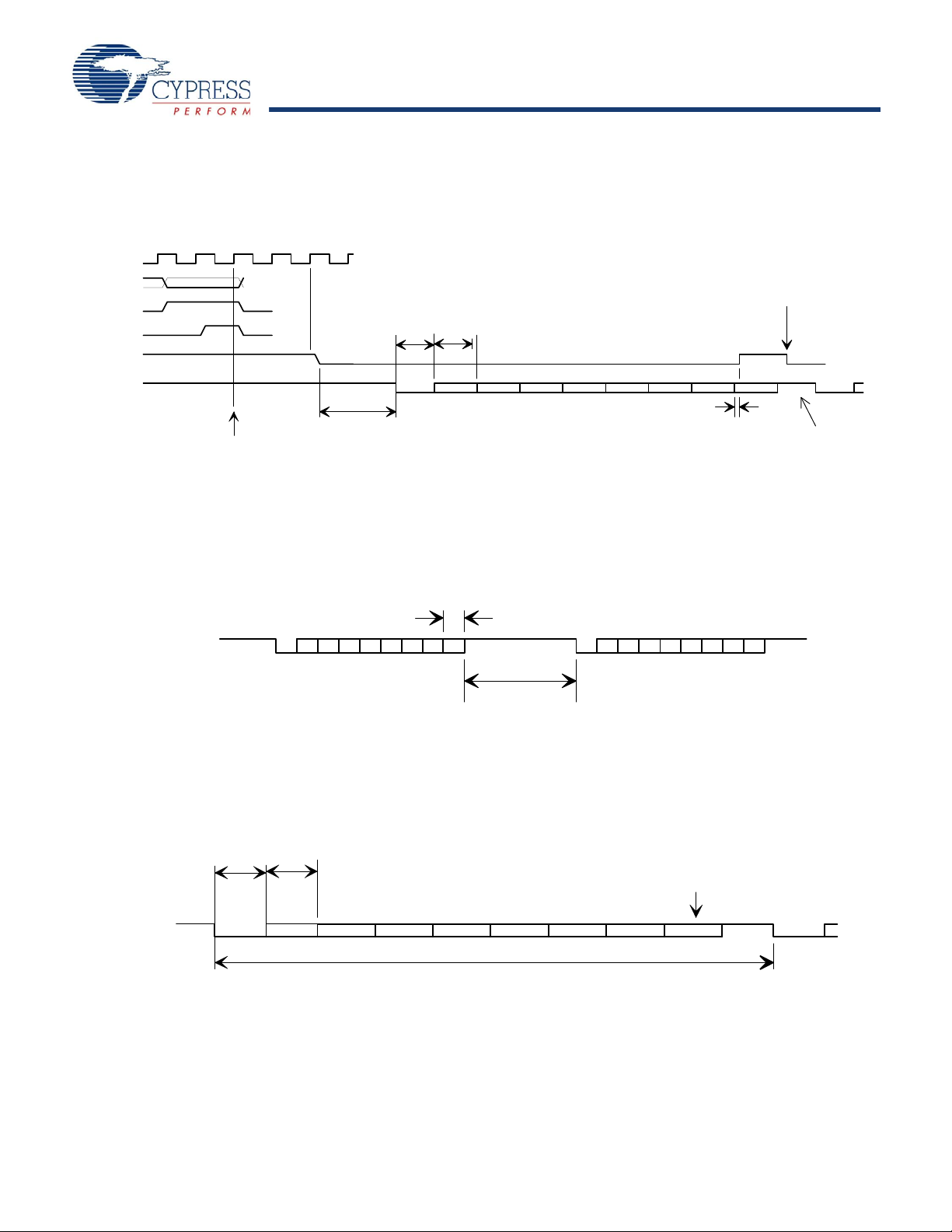
CY7C67300
IDE Timing
CPU may start another BYTE
transmit right after TxRdy
goes high
start of last data bit to TxRdy high:
0 min, 4 T max.
(T is qt_clk period)
TxRdy low to start bit delay:
0 min, BT max when starting from IDEL.
For back to back transmit, new START Bit
begins immediately following previous STOP bit.
(BT = bit period)
BT
BT
start bit bit 0
bit 1 bit 2 bit 3 bit 4 bit 5 bit 6 bit 7
qt_clk
CPU_A[2:0]
CPUHSS_cs
CPU_wr
TxRdy flag
HSS_TxD
Byte transmit
triggered by a
CPU write to the
HSS_TxData register
stop bit start bit
programmable
1 or 2 stop bits.
1 stop bit shown.
HSS_TxD
t
GAP
BT
BT +/- 5%
start bit bit 0
bit 1 bit 2 bit 3 bit 4 bit 5 bit 6 bit 7 stop bit start bit
HSS_RxD
BT +/- 5%
10 BT +/- 5%
received byte added to
receive FIFO during the final data bit time
The IDE interface supports PIO mode 0-4 as specified in the Information Technology-A T Attachment–4 with Packet Interface Extension
(ATA/ATAPI-4) Specification, T13/1153D Rev 18.
HSS BYTE Mode Transmit
qt_clk, CPU_A, CPUHSS_cs, CPU_wr are internal signals, included in the diagram to illustrate the relationship between CPU operations and HSS port operations.
Bit 0 is LSB of data byte. Data bits are HIGH true: HSS_TxD HIGH = data bit value ‘1’.
BT = bit time = 1/baud rate.
HSS Block Mode Tra nsmit
BLOCK mode transmit timing is similar to BYTE mode, except the STOP bit time is controlled by the HSS_GAP value.
The BLOCK mode STOP bit time, t
Transmit Gap register [0xC074].
The default t
GAP
is 2 BT.
= (HSS_GAP – 9) BT, where BT is the bit time, and HSS_GAP is the content of the HSS
GAP
BT = bit time = 1/baud rate.
HSS BYTE and BLOCK Mode Receive
Receive data arrives asynchronously relative to the internal clock. Incoming data bit rate may deviate from the programmed baud rate
clock by as much as ±5% (with HSS_RATE value of 23 or higher).
BYTE mode received bytes are buffered in a FIFO. The FIFO not empty condition becomes the RxRdy flag.
BLOCK mode received bytes are written directly to the memory system.
Bit 0 is LSB of data byte. Data bits are HIGH true: HSS_RxD HIGH = data bit value ‘1’.
BT = bit time = 1/baud rate.
Document #: 38-08015 Rev. *J Page 91 of 99
[+] Feedback
Page 92
CY7C67300
Hardware CTS/RTS Handshake
tCTSsetup
tCTSsetup
Start of transmission delayed until HSS_CTS goes high
Start of transmission not delayed by HSS_CTS
tCTShold
tCTShold
HSS_RTS
HSS_CTS
HSS_TxD
t
CTSsetup
t
CTShold
: HSS_CTS setup time before HSS_RTS = 1.5T min.
: HSS_CTS hold time after START bit = 0 ns min.
T = 1/48 MHz.
When RTS/CTS hardware handshake is enabled, transmission can be help off by deasserting HSS_CTS at least 1.5T before
HSS_RTS. Transmission resumes when HSS_CTS returns HIGH. HSS_CTS must remain HIGH until START bit.
HSS_RTS is deasserted in the third data bit time.
An application may choose to hold HSS_CTS until HSS_RTS is deasserted, which always occurs after the START bit.
Register Summary
Table 142. Register Summary
R/W Address Register Bit 15 Bit 14 Bit 13 Bit 12 Bit 11 Bit 10 Bit 9 Bit 8 Default High
R 0x0140 HPI Breakpoint Address... 0000 0000
R 0x0142 Interrupt Routing VBUS to HPI
W 1: 0x0144
R/W 0x02n0 Device n Endpoint n Control Reserved xxxx xxxx
R/W 0x02n2 Device n Endpoint n Address Address... xxxx xxxx
R.W 0x02n4 Device n Endpoint n Count Reserved Count... xxxx xxxx
R/W 0x02n6 Device n Endpoint n Status Reserved Overflow
R/W 0x02n8 Device n Endpoint n Count Result Result... xxxx xxxx
R 0xC000 CPU Flags Reserved... 0000 0000
R/W 0xC002 Bank Address... 0000 0001
R 0xC004 Hardware Revision Revision... xxxx xxxx
R/W 0xC006 GPIO Control Write Protect
R/W 0xC008 CPU Speed Reserved... 0000 0000
R/W 0xC00A Power Control Host/Device
SIEXmsg Data... xxxx xxxx
2: 0x0148
Bit 7 Bit 6 Bit 5 Bit 4 Bit 3 Bit 2 Bit 1 Bit 0 Default Low
...Address 0000 0000
Enable
Resume2 to
HPI Enable
...Data xxxx xxxx
IN/OUT
Ignore Enable
...Address xxxx xxxx
...Count xxxx xxxx
Stall
Flag
...Result xxxx xxxx
...Reserved Global Inter-
...Address Reserved 000x xxxx
...Revision xxxx xxxx
Enable
HSS
Enable
.Reserved CPU Speed 0000 1111
2B Wake
Enable
HPI
Wake Enable
ID to HPI
Enable
Resume1 to
HPI Enable
Sequence
Select
NAK
Flag
UD Reserved SAS
HSS XD
Enable
Host/Device
2A Wake
Enable
Reserved GPI
SOF/EOP2 to
HPI Enable
Reserved Done2 to HPI
Stall
Enable
Length
Exception Flag
SPI
Enable
Host/Device
1B Wake
Enable
SOF/EOP2 to
CPU Enable
ISO
Enable
Setup
Flag
rupt Enable
SPI XD
Enable
Host/Device
1A Wake
Enable
Wake Enable
SOF/EOP1 to
HPI Enable
Enable
NAK Interrupt
Enable
Flag
Sequence
Status
Negative
Flag
Enable
Interrupt 1
Polarity
Select
OTG
Wake
Enable
Reserved Boost 3V OKSleep
SOF/EOP1 to
CPU Enable
Done1 to HPI
Enable
Direction
Select
Underflow
Flag
Timeout
Flag
Overflow
Flag
Mode
Select
Interrupt 1
Enable
Reserved HSS
Reset2 to HPI
Enable
Reset1 to HPI
Enable
Enable ARM
OUT
Exception FlagINException Flag
Error
Flag
Carry
Flag
Interrupt 0
Polarity
Select
Wake
Enable
Enable
HPI Swap 1
Enable
HPI Swap 0
Enable
Enable
ACK
Flag
Zero
Flag
Interrupt 0
Enable
SPI
Wake
Enable
Halt
Enable
0001 0100
0000 0000
xxxx xxxx
xxxx xxxx
xxxx xxxx
000x xxxx
0000 0000
0000 0000
0000 0000
0000 0000
Document #: 38-08015 Rev. *J Page 92 of 99
[+] Feedback
Page 93

CY7C67300
Table 142. Register Summary (continued)
R/W Address Register Bit 15 Bit 14 Bit 13 Bit 12 Bit 11 Bit 10 Bit 9 Bit 8 Default High
R/W 0xC00C Watchdog Timer Reserved... 0000 0000
R/W 0xC00E Interrupt Enable Reserved OTG Interrupt
R/W 0xC098 OTG Control Reserved VBUS
R/W 0: 0xC010
R/W 0xC014 Breakpoint Address... 0000 0000
R/W 1: 0xC018
R/W 0: 0xC01E
R0: 0xC020
R/W 0: 0xC022
R/W 0xC038 Upper Address Enable Reserved xxxx xxxx
R/W 0xC03A External Memory Control Reserved XRAM
R/W 0xC03C USB Diagnostic Port 2B
W 0xC03E Memory Diagnostic Reserved Memory
R/W 0xC048 IDE Mode Reserved... 0000 0000
R/W 0xC04A IDE Start Address Address... 0000 0000
R/W 0xC04C IDE Stop Address Address... 0000 0000
R/W 0xC04E IDE Control Reserved... 0000 0000
- 0xC050-0
R/W 0xC070 HSS Control HSS
R/W 0xC072 HSS Baud Rate Reserved HSS Baud... 0000 0000
R/W 0xC074 HSS Transmit Gap Reserved
R/W 0xC076 HSS Data Reserved xxxx xxxx
R/W 0xC078 HSS Receive Address Address... 0000 0000
R/W 0xC07A HSS Receive Counter Reserved Counter... 0000 0000
R/W 0xC07C HSS Transmit Address Address.. 0000 0000
Timer n Count... 1111 1111
1: 0xC012
Extended Page n Map Address... 0000 0000
2: 0xC01A
GPIO n Output Data Data... 0000 0000
1: 0xC024
GPIO n Input Data Data... 0000 0000
1: 0xC026
GPIO n Direction Direction Select... 0000 0000
1: 0xC028
IDE PIO Port
xC06E
Bit 7 Bit 6 Bit 5 Bit 4 Bit 3 Bit 2 Bit 1 Bit 0 Default Low
...Reserved Timeout
HSS
Interrupt
Enable
D+ Pulldown
Enable
...Count 1111 1111
...Address 0000 0000
...Address 0000 0000
...Data 0000 0000
...Data 0000 0000
...Direction Select 0000 0000
Reserved Upper
XROM
Width Select
Diagnostic
Enable
...Reserved Pull-down
Reserved Monitor
...Reserved Reserved Mode Select 0000 0000
... Address 0000 0000
...Address 0000 0000
...Reserved Direction
Enable
Transmit Done
Interrupt Flag
...Baud 0001 0111
Transmit Gap Select 0000 1001
Data xxxx xxxx
...Address 0000 0000
...Counter 0000 0000
...Address 0000 0000
In Mailbox
Interrupt
Enable
D– Pull-down
Enable
XROM
Wait Select
Port 2A
Diagnostic
Enable
Enable
RTS
Polarity
Select
Receive Done
Interrupt Flag
Flag
Out Mailbox
Interrupt
Enable
Pull-up
Enable
Reserved OTG Data
Merge Enable
Port 1B
Diagnostic
Enable
LS Pull-up
Enable
CTS
Polarity
Select
One
Stop Bit
Period
Select
Enable
Reserved UART
Receive
Disable
XROM
Merge Enable
Port 1A
Diagnostic
Enable
FS Pull-up
Enable
XOFF XOFF
Transmit
Ready
SPI Interrupt
Enable
Interrupt
Enable
Charge Pump
Enable
Address
Enable
XMEM
Width Select
XRAM
Width Select
Reserved... 0000 0000
Reserved Force Select 0000 0000
Select
Enable
Packet Mode
Select
Lock
Enable
Reserved Host/Device 2
GPIO
Interrupt
Enable
VBUS
Discharge
Enable
Status
Reserved xxxx 0xxx
XMEM
Wait Select
XRAM
Wait Select
Arbitration
Select
IDE Interrupt
Enable
CTS
Enable
Receive
Overflow Flag
WDT
Enable
Interrupt
Enable
Timer 1
Interrupt
Enable
D+
Pull-up
Enable
ID
Status
Done
Flag
Receive
Interrupt
Enable
Receive Packet Ready Flag
Reset
Strobe
Host/Device 1
Interrupt
Enable
Timer 0
Interrupt
Enable
D–
Pull-up
Enable
VBUS Valid
Flag
Enable
IDE
Enable
Done
Interrupt
Enable
Receive
Ready Flag
0000 0000
0000 0000
0001 0000
0000 0000
0000 0xxx
xxxx xxxx
xxxx xxxx
0000 0000
0000 0000
0000 0000
0000 0000
0000 0000
0000 0000
Document #: 38-08015 Rev. *J Page 93 of 99
[+] Feedback
Page 94

CY7C67300
Table 142. Register Summary (continued)
R/W Address Register Bit 15 Bit 14 Bit 13 Bit 12 Bit 11 Bit 10 Bit 9 Bit 8 Default High
R/W 0xC07E HSS Transmit Counter Reserved Counter... 0000 0000
R/W 0xC080
R/W 0xC082
R/W 0xC084
R/W 0xC084
R 0xC086
W 0xC086
R 0xC088
W 0xC088
R/W 0xC08A
R/W 0xC08C Host 1 Interrupt Enable VBUS
R/W 0xC08C Device 1 Interrupt Enable VBUS
R/W 0xC08E
R/W 0xC090 Host 1 Status VBUS
R/W 0xC090 Device 1 Status VBUS
R/W 0xC092
R 0xC092
R 0xC094
W 0xC094
R 0xC096
R/W 0xC0AC Host 2 Interrupt Enable Reserved SOF/EOP
Host n Control Reserved 0000 0000
0xC0A0
Host n Address Address... 0000 0000
0xC0A2
Host n Count Reserved Port Select Reserved Count... 0000 0000
0xC0A4
Device n Port Select Reserved Port Select Reserved... 0000 0000
0xC0A4
Host n PID Reserved Overflow
0xC0A6
Host n EP Status Reserved 0000 0000
0xC0A4
Host n Count Result Result... 0000 0000
0xC0A8
Host n Device Address Reserved... 0000 000 0
0xC0A8
USB n Control Port B
0xC0AA
Device n Address Reserved... 0000 0000
0xC0AE
Host n SOF/EOP Count Reserved Count... 0010 1110
0xC0B2
Device n Frame Number SOF/EOP
0xC0B2
Host n SOF/EOP Counter Reserved Counter... xxxx xxxx
0xC0B4
Device n SOF/EOP Count Reserved Count... 0010 1110
0xC0B4
Host n Frame Reserved Frame... 0000 0000
0xC0B6
Bit 7 Bit 6 Bit 5 Bit 4 Bit 3 Bit 2 Bit 1 Bit 0 Default Low
...Counter 0000 0000
Preamble
Enable
...Address 0000 0000
...Count 0000 0000
...Reserved 0000 0000
Stall
Flag
PID Select Endpoint Select 0000 0000
...Result 0000 0000
...Reserved Address 0000 0000
D+ Status
Port A
Resistors
Enable
Interrupt
Enable
Port B
Wake Interrupt
Enable
Interrupt
Enable
EP7
Interrupt
Enable
...Reserved Address 0000 0000
Interrupt FlagIDInterrupt Flag
Port B
Wake Interrupt
Flag
Interrupt FlagIDInterrupt Flag
EP7
Interrupt Flag
...Count 1110 0000
Timeout
Flag
...Frame 0000 0000
...Counter xxxx xxxx
...Count 1110 0000
...Frame 0000 0000
Port B
Wake Interrupt
Enable
Sequence
Select
NAK
Flag
Port B
D– Status
Port B
Force D+/State
ID
Interrupt
Enable
Port A
Wake Interrupt
Enable
ID
Interrupt
Enable
EP6
Interrupt
Enable
Port A
Wake Interrupt
Flag
EP6
Interrupt Flag
SOF/EOP
Timeout
Interrupt Count
Port A
Wake Interrupt
Enable
Sync
Enable
Length
Exception Flag
Port A
D+ Status
Reserved SOF/EOP
Port B Connect
Change
Interrupt Enable
Reserved SOF/EOP
EP5
Interrupt
Enable
Reserved SOF/EOP
Port B Connect
Change
Interrupt Flag
Reserved SOF/EOP
EP5
Interrupt Flag
Port B Connect
Change
Interrupt
Enable
ISO
Enable
Reserved Sequence
Port A
D– Status
Port A
Force D±
State
Port A Connect Change
Interrupt
Enable
EP4
Interrupt
Enable
Port A Connect Change
Interrupt Flag
EP4
Interrupt Flag
Port A Connect Change
Interrupt
Enable
Reserved Arm
Flag
Status
LOB LOA Mode
Reserved Done
Timeout Interrupt Enable
EP3
Interrupt
Enable
Port B
SE0
Status
EP3
Interrupt Flag
Reserved Frame... 0000 0000
Reserved Done
Underflow
Flag
Timeout
Flag
Suspend
Enable
Reserved SOF/EOP
EP2
Interrupt
Enable
Port A
SE0
Status
EP2
Interrupt Flag
Reserved 0000 0000
Error
Flag
Select
Port B
SOF/EOP
Enable
Interrupt
Enable
Interrupt
Enable
EP1
Interrupt
Enable
Interrupt Flag
Reserved Done
Interrupt Flag
EP1
Interrupt Flag
Interrupt
Enable
Enable
ACK
Flag
Port B Resistors Enable
Port A
SOF/EOP
Enable
Reserved 0000 0000
Interrupt
Enable
Reset
Interrupt
Enable
EP0
Interrupt
Enable
Reserved xxxx xxxx
Interrupt
Flag
Reset
Interrupt Flag
EP0
Interrupt Flag
Reserved 0000 0000
Interrupt
Enable
0000 0000
0000 0000
xxxx 0000
0000 0000
0000 0000
0000 0000
0000 0000
xxxx xxxx
xxxx xxxx
xxxx xxxx
0000 0000
Document #: 38-08015 Rev. *J Page 94 of 99
[+] Feedback
Page 95

CY7C67300
Table 142. Register Summary (continued)
R/W Address Register Bit 15 Bit 14 Bit 13 Bit 12 Bit 11 Bit 10 Bit 9 Bit 8 Default High
R/W 0xC0AC Device 2 Interrupt Enable Reserved SOF/EOP
R/W 0xC0B0 Host 2 Status Reserved SOF/EOP
R/W 0xC0B0 Device 2 Status Reserved SOF/EOP
R/W 0xC0C6 HPI Mailbox Message... 0000 0000
R/W 0xC0C8 SPI Configuration 3Wire
R/W 0xC0CA SPI Control SCK
R/W 0xC0CC SPI Interrupt Enable Reserved... 0000 0000
R 0xC0CE SPI Status Reserved... 0000 0000
W 0xC0D0 SPI Interrupt Clear Reserved... 0000 0000
R/W 0xC0D2 SPI CRC Control CRC Mode CRC
R/W 0xC0D4 SPI CRC Value CRC 1111 1111
R/W 0xC0D6 SPI Data Port t Reserved xxxx xxxx
R/W 0xC0D8 SPI Transmit Address Address... 0000 0000
R/W 0xC0DA SPI Transmit Count Reserved Count... 0000 0000
R/W 0xC0DC SPI Receive Address Address... 0000 0000
R/W 0xC0DE SPI Receive Count Reserved Count... 0000 0000
R/W 0xC0E0 UART Control Reserved... 0000 0000
R 0xC0E2 UART Status Reserved... 0000 0000
R/W 0xC0E4 UART Data Reserved 0000 0000
R/W 0xC0E6 PWM Control PWM
R/W 0xC0E8 PWM Maximum Count Reserved Count... 0000 0000
R/W 0:
PWM n Start Reserved Address... 0000 0000
0xC0EA
1:
0xC0EE
2: 0xC0F2
3: 0xC0F6
Bit 7 Bit 6 Bit 5 Bit 4 Bit 3 Bit 2 Bit 1 Bit 0 Default Low
Timeout
Interrupt
EP7
Interrupt
Enable
Port B
Wake Interrupt
Flag
EP7
Interrupt Flag
...Message 000 0 000 0
Enable
Master
Active Enable
Strobe
Transmit
Empty
...Reserved Receive Inter-
FIFO Error
Flag
...Reserved Transmit
...Reserved 0000 0000
...CRC 1111 1111
Data xxxx xxxx
...Address 0000 0000
...Count 0000 0000
...Address 0000 0000
...Count 0000 0000
...Reserved Scale Select Baud Select UART Enable 0000 0111
...Reserved Receive
Data 0000 000 0
Enable
PWM3
Polarity Select
...Count 0000 0000
...Address 0000 0000
EP6
Interrupt
Enable
Port A
Wake Interrupt
Flag
EP6
Interrupt Flag
Phase
Select
Master
Enable
FIFO
Init
Receive
Full
Reserved Receive
Reserved Prescale
PWM2
Polarity Select
EP5
Interrupt
Enable
Port B
Connect
Change
Interrupt Flag
EP5
Interrupt Flag
SCK
Polarity Select
SS
Enable
Byte
Mode
Transmit Bit Length Receive Bit Length 1000 0000
Enable
PWM1
Polarity Select
EP4
Interrupt
Enable
Port A
Connect
Change
Interrupt Flag
EP4
Interrupt Flag
Scale Select Reserved 1000 0000
SS Delay Select 0001 1111
FullDuplex SS
CRC
Clear
PWM0
Polarity Select
Enable
EP3
Interrupt
Enable
Port B
SE0
Status
Timeout
Interrupt
Enable
EP3
Interrupt Flag
Manual
Receive
CRC
Select
PWM3
Enable
Wake
Interrupt
Enable
EP2
Interrupt
Enable
Port A
SE0
Status
Wake
Interrupt
Flag
EP2
Interrupt Flag
Read
Enable
rupt Enable
Interrupt Flag
One in CRC Zero in CRC Reserved... 0000 0000
PWM2
Enable
SOF/EOP
Interrupt
Enable
EP1
Interrupt
Enable
Interrupt
Flag
Reserved Done
SOF/EOP
Interrupt
Flag
EP1
Interrupt Flag
Transmit
Ready
Transmit Interrupt Enable
Transmit
Interrupt Flag
Interrupt Clear
Full
PWM1
Enable
Reset
Interrupt
Enable
EP0
Interrupt
Enable
Reserved xxxx xxxx
Interrupt
Flag
Reset
Interrupt
Flag
EP0
Interrupt Flag
receive
Data Ready
Transfer Interrupt Enable
Transfer
Interrupt Flag
Transmit
Interrupt Clear
Transmit
Full
Mode
Select
PWM0
Enable
0000 0000
0000 0000
xxxx xxxx
xxxx xxxx
xxxx xxxx
0000 0001
0000 0000
0000 0000
0000 0000
0000 0000
0000 0000
0000 0000
Document #: 38-08015 Rev. *J Page 95 of 99
[+] Feedback
Page 96

CY7C67300
Table 142. Register Summary (continued)
R/W Address Register Bit 15 Bit 14 Bit 13 Bit 12 Bit 11 Bit 10 Bit 9 Bit 8 Default High
R/W 0:
R/W 0xC0FA PWM Cycle Count Count... 0000 0000
R HPI Status Port VBUS
PWM n Stop Reserved Address... 0000 0000
0xC0EC
1: 0xC0F0
2: 0xC0F4
3: 0xC0F8
Bit 7 Bit 6 Bit 5 Bit 4 Bit 3 Bit 2 Bit 1 Bit 0 Default Low
...Address 0000 0000
...Count 0000 0000
Flag
Resume2 Flag Resume1 Flag SIE2msg SIE1msg Done2 Flag Done1 Flag Reset1 Flag Mailbox Out
ID
Flag
Reserved SOF/EOP2
Flag
Reserved SOF/EOP1
Flag
Reset2
Flag
Mailbox In
Flag
Flag
Document #: 38-08015 Rev. *J Page 96 of 99
[+] Feedback
Page 97

CY7C67300
Ordering Information
NOTE:
1. JEDEC STD REF MS-026
2. BODY LENGTH DIMENSION DOES NOT INCLUDE MOLD PROTRUSION/END FLASH
MOLD PROTRUSION/END FLASH SHALL NOT EXCEED 0.0098 in (0.25 mm) PER SIDE
3. DIMENSIONS IN MILLIMETERS
BODY LENGTH DIMENSIONS ARE MAX PLASTIC BODY SIZE INCLUDING MOLD MISMATCH
0.22±0.05
0.50
14.00±0.05 SQ
16.00±0.25 SQ
1.40±0.05
12°±1°
1.60 MAX.
0.05 MIN.
0.60±0.15
0° MIN.
0.25
0°-7°
(8X)
STAND-OFF
R 0.08 MIN.
TYP.
GAUGE PLANE
0.20 MAX.
0.15 MAX.
0.20 MAX.
1
100
R0.08MIN.
0.20 MAX.
76
75
5125
26 50
0.20 MIN.
1.00 REF.
0.08
SEE DETAIL
A
DETAIL
A
SEATING PLANE
NOTE: PKG. CAN HAVE
OR
TOP LEFT CORNER CHAMFER 4 CORNERS CHAMFER
51-85048-*C
Table 143. Ordering Information
Ordering Code Package Type AEC Pb-Free Temperature Range
CY7C67300-100AXI 100 TQFP X –40 to 85°C
CY7C67300-100AXA 100 TQFP X X –40 to 85°C
CY7C67300-100AXIT 100 TQFP, tape and reel X –40 to 85°C
CY7C67300-100AXAT 100 TQFP, tape and reel X X –40 to 85°C
CY3663 Development Kit
Package Diagrams
Figure 12. 100-Pin Thin Plastic Quad Flat Pack (TQFP) A100SA
Document #: 38-08015 Rev. *J Page 97 of 99
[+] Feedback
Page 98

CY7C67300
Document History Page
Document Title: CY7C67300 EZ-Host™ Programmable Embedded USB Host and Peripheral Contro ller with Automotive
AEC Grade Support
Document Number: 38-08015
REV. ECN NO.
** 111872 MUL 03/22/02 New Data Sheet
*A 116989 MUL 08/23/02 Preliminary Data Sheet
*B 125262 MUL 04/10/03 Added Memory Map Section and Ordering Information Section
*C 126210 MUL 05/23/03 Added Interface Description Section and Power Savings and Reset Section
*D 127335 KKV 05/29/03 Corrected font to enable correct symbol display
*E 129395 MUL 10/01/03 Final Data Sheet
*F 443992 VCS See ECN Title changed indicating AEC Grade
*G 566465 KKVTMP See ECN Added the lead free information on the Ordering Information Section. Imple-
*H 1063560 ARI See ECN Changed Ordering Informatijon table to reflect Automotive Qualification and to
*I 2514867 PYRS See ECN To publish in Web
*J 2544823 BHA/AESA 07/28/08 Updated template. Corrected A18 and A17 pin assignments in T ables 6 and 131.
Orig. of
Change
Submis-
sion Date
Description of Change
Moved Functional Register Map Tables into Register secti on
General Clean-up
Added Char Data
General Clean-up
Changed Memory Map Section and added CLKSEL to Pin Description
Added USB OTG Logo
General Clean-up
Added information for AEC qualified including part number
Fixed misc. errors including:
Table 4-1: UART does not have alternate location
Section 4.3.4 had incorrect register address
Table 4-10 had incorrect pin definitions
Section 4.16.2 changed GPIO[31:20] to GPIO[31:30]
Corrected Table 7-6 and 7-14
mented the new template with no numbers on the headings.
meet the MPN Part Number changes reflected in ECN 884880.
Changed the EZ-Host Pin Diagram figure to reflect the pin changes. Edited.
Document #: 38-08015 Rev. *J Page 98 of 99
[+] Feedback
Page 99

CY7C67300
Sales, Solutions, and Legal Information
Worldwide Sales and Design Support
Cypress maintains a worldwide network of offices, solution centers, manufacturer’s representatives, and distributors. To find the office
closest to you, visit us at cypress.com/sales.
Products
PSoC psoc.cypress.com
Clocks & Buffers clocks.cypress.com
Wireless wireless.cypress.com
Memories memory.cypress.com
Image Sensors image.cypress.com
PSoC Solutions
General psoc.cypress.com/solutions
Low Power/Low Voltage psoc.cypress.com/low-power
Precision Analog psoc.cypress.com/precision-analog
LCD Drive psoc.cypress.com/lcd-drive
CAN 2.0b psoc.cypress.com/can
USB psoc.cypress.com/usb
© Cypress Semiconductor Corporation, 2002-200 8. The inform ation cont ained herein is subject to change witho ut notice. Cypr ess Semiconductor Corporation assumes no responsibility for the use of
any circuitry other than circuitry embodied in a Cypress product. Nor does it convey or imply any license under patent or other rights. Cypress products are not warranted nor intend ed to be us ed for
medical, life support, life saving, critical contr o l o r saf ety ap pl ic at io ns, unl ess pu r suan t to a n exp re ss wr itte n agreement with Cypress. Furthermore, Cypress does not authorize its products for use as
critical components in life-support systems where a malfunction or failur e may reasonably be expe cted to result in significa nt injury to the u ser . The inclu sion of Cypress p roducts in life -support systems
application implies that the manufacturer assumes all risk of such use and in doing so indemnifies Cypress against all charges.
Any Source Code (software and/or firmware) is owned by Cypress Semiconductor Corporation (Cypress) and is protected by and subject to worldwide patent protectio n (United States and foreign),
United States copyrigh t laws and in ternati onal trea ty provis ions. Cyp ress he reby gra nt s to lic ensee a p erson al, no n-exclu sive, no n-tran sferab le license to copy, use, modify, crea te derivati ve works of ,
and compile the Cypress Source Code and derivative works for the sole purpose of creating custom software and or firmware in support of licensee product to be used only in conjuncti on with a Cypress
integrated circuit as specified in the ap plicable agreem ent. Any reprod uction, modificatio n, translation, com pilation, or repr esentation of this Source Co de except as speci fied above is pro hibited with out
the express written permission of Cypress.
Disclaimer: CYPRESS MAKES NO WARRANTY OF ANY KIND, EXPRESS OR IMPLIED, WITH REGARD TO THIS MATERIAL, INCLUDING, BUT NOT LIMITED TO, THE IMPLIED WARRANTIES
OF MERCHANTABILITY AND FITNESS FOR A PARTICULAR PURPOSE. Cypress reserves the right to make changes without further notice to the materials described herein. Cypress does not
assume any liability arising out of the applica tion or use o f any produ ct or ci rcuit de scrib ed herei n. Cy press does n ot auth orize it s product s for use a s critical componen ts in life-suppo rt systems where
a malfunction or failure may reason ably be expected to res ult in significant inj ury to the user. The inclusion of Cypre ss’ product in a life-support systems application implies that the manufacturer
assumes all risk of such use and in doing so indemnifies Cypress against all charges.
Use may be limited by and subject to the applicable Cypress software license agreement.
Document #: 38-08015 Rev. *J Revised July 28, 2008 Page 99 of 99
EZ-Host is a registered trad emark of Cypress Semi conductor Corp. All other trademarks or registered trademar ks referenced herei n are property of the respective corporations. Purchase of I2C
components from Cypress or one of its sublicensed Ass ociated Com pan ies conveys a lice nse under the Philips I2C Patent R ight s to use these compo nents in an I2C syste m, provided that the system
conforms to the I2C Standard Specification as defined by Philips. All products and company names mentioned in this document may be the trademarks of their respective holders.
[+] Feedback
 Loading...