

Page 1

C66011
CY7C66013
CY7C66113
CY7C66013
CY7C66113
Full-Speed USB (12 Mbps) Peripheral
Controller with Integrated Hub
Cypress Semiconductor Corporation • 3901 North First Street • San Jose • CA 95134 • 408-943-2600
Document #: 38-08024 Rev. ** Revised March 26, 2002
Page 2

CY7C66013
CY7C66113
TABLE OF CONTENTS
1.0 FEATURES .....................................................................................................................................6
2.0 FUNCTIONAL OVERVIEW ...... ...................... ........................ ............................................. ............7
3.0 PIN CONFIGURATIONS ..................................... .. .. .. ................................. .....................................9
4.0 PRODUCT SUMMARY TABLES ..................................................................................................10
4.1 Pin Assignments . .............. .. ............. .. .............. .. ............. .. .. .............. .. ............. .. .........................10
4.2 I/O Registe r Su mmary ......... ............. .. .............. .. ............. .. ............. ... ............. ............. .. .. ............10
4.3 Instruction Set Summary ............................................................................................................12
5.0 PROGRAMM I N G M OD E L ..... .. .. .............. .. ............. .. ............. ... ............. .. ............. ... ............. .. .......13
5.1 14-Bit Program Counter (PC) ......................................................................................................13
5.1.1 Program Memory Organization .........................................................................................................14
5.2 8-Bit Accumu la tor (A) ............ .. .. .............. .. ............. .. .............. .. .. ............. ... ............. .. ..................14
5.3 8-Bit Temporary Register (X) ......................................................................................................14
5.4 8-Bit Program Stack Pointer (PSP) ............................................................................................15
5.4.1 Data Memory Organization ................................................................................................................15
5.5 8-Bit Data Stack Pointer (DSP) ................................................................................................... 15
5.6 Address Mo d e s ............... ... ............. .. ............. ... ............. .. ............. .. .............. .. ............. ................16
5.6.1 Data (Immediate) .................................................................................................................................16
5.6.2 Direct ...................................................................................................................................................16
5.6.3 Indexed ................................................................................................................................................16
6.0 CLOCKING ....................................................................................................................................16
7.0 RESET ................................................................. ..........................................................................17
7.1 Power-On Reset (POR) ................................................................................................................17
7.2 Watch Dog Reset (WDR) .............................................................................................................17
8.0 SUSPEND MODE ............................ .. .. .. .................................. .. .. .. .. .. ............................................18
9.0 GENERAL-PURPOSE I/O (GPIO) PORTS ...................................................................................18
9.1 GPIO Configuration Port .............................................................................................................19
9.2 GPIO Interrupt Enable Ports .......................................................................................................20
10.0 DAC PORT ..................................................................................................................................21
10.1 DAC Isink Registers ..................................................................................................................21
10.2 DAC Port Interrupts ...................................................................................................................22
11.0 12-BIT FREE-RUNNING TIMER ............................................................ .. ............................. ......22
11.1 Timer (LSB ) ........ ... .. ............. .. .............. .. ............. .. ............. ... ............. .. ............. ... ......................22
11.2 Timer (MSB) .... ............. .. .............. .. ............. .. ... ............. .. ............. .. .............. .. .............................22
12.0 I
13.0 I
2
C AND HAPI CONFIGURATION REGISTER ..........................................................................23
2
C COMPATIB L E CO N T R O L L ER ......... ............. .. ............. ... ............. .. ............. ... ............. .. .. .....24
14.0 HARDWARE ASSISTED PARALLEL INTERFACE (HAPI) .................................... .. .. .. .............25
15.0 PROCESSOR STATUS AND CONTROL REGISTER ................................. .. ............................26
16.0 INTERRUPTS ..............................................................................................................................27
16.1 Interrup t V e c to r s ........... ... ............. .. ............. ... ............. .. ............. .. .............. .. .............................28
16.2 Interrup t L a te n c y ..................... ... ............. .. ............. ... ............. .. .. .............. .. ............. ..................30
16.3 USB Bus Reset Interrupt ...........................................................................................................30
16.4 Timer Inter rupt .......... .. ............. ... ............. .. ............. ... ............. .. ............. ... ............. .. ..................30
Document #: 38-08024 Rev. ** Page 2 of 53
Page 3

CY7C66013
CY7C66113
16.5 USB Endpoint Interrup ts ....... .............. .. ............. .. ............. ... ............. .. .. .............. .. ....................30
16.6 USB Hub Int e rr u p t ................... ... ............. .. ............. ... .. ............. .. .............. .. ............. .. ................30
16.7 DAC Interrupt .............................................................................................................................31
16.8 GPIO/HAPI Interrupt ..................................................................................................................31
16.9 I
17.0 USB OVERV I E W .......... .. .............. .. ............. .. ... ............. .. ............. .. .............. .. ............. .. . .............32
17.1 USB Serial Interface Engine (SIE) ..................................................................... .......................32
17.2 USB Enume ra tion ....... .. .............. .. .. ............. ... ............. .. ............. .. .............. .. ............. .. . .............32
18.0 USB HUB ....................................................................................................................................33
18.1 Connecting/Disconnecting a USB Device ...............................................................................33
18.2 Enablin g/ D is a b l in g a U SB D e vice .......... .. ............. ... ............. .. ............. ... ............. ............. .. .....34
18.3 Hub Downstream Ports Status and Control ............................................................................34
18.4 Downstream Port Suspend and Resume ................................................................................35
18.5 USB Upstream Port Status and Control ..................................................................................36
19.0 USB SERIAL IN T E R F A CE ENGINE OP ER A T ION ..................... .. .............. .. ............. .. ..............37
19.1 USB Device Addresses .............................................................................................................37
19.2 USB Device Endpoints ..............................................................................................................37
19.3 USB Contr o l E n dp o i n t M o d e Re g i sters ... .. .............. .. ............. .. .............. .. ............. .. ............. ...38
19.4 USB Non-Control Endpoint Mode Registers ............................... ............................................38
19.5 USB Endpoint Counter Registers ............................................................................................39
19.6 Endpoint Mode/Count Registers Update and Locking Mechanism ....................... ...............39
20.0 USB MODE T A B L E S .............. .............. .. ............. .. ............. ... ............. .. ............. ... ............. .........41
2
C Interrupt ........................ ............. .. .............. .. ............. .. ............. ... ............. .. ............. . .............31
21.0 SAMPLE SC H E M ATIC ............. ... ............. .. ............. ... ............. ............. .. .............. .. ....................45
22.0 ABSOLUTE M A X I M U M R A T INGS ......... ............. .. .. .............. .. ............. .. .............. .. ............. .. .....46
23.0 ELECTRICAL CHARACTERISTICS ............................................... ............................................46
24.0 SWITCHING CHARACTERISTICS ............................................... .. ................................ ............48
25.0 ORDERIN G IN F O RMATION .............. ... ............. .. .. ............. ... ............. .. ............. ... ............. .. .......50
26.0 PACKAGE DIAGRAMS ................................. ................................. ............................................51
Document #: 38-08024 Rev. ** Page 3 of 53
Page 4

CY7C66013
CY7C66113
LIST OF FIGURES
Figure 5-1. Program Memory Space with Interrupt Vector Table ..................................................14
Figure 6-1. Clock Oscillator On-Chip Circuit ...................................................................................16
Figure 7-1. Watch Dog Reset (WDR) .......................................... ............................................ ..........17
Figure 9-1. Block Diagram of a GPIO Pin ........................................................................................ 18
Figure 9-2. Port 0 Data 0x00 (read/write) ................................... .......................... .. ..........................19
Figure 9-3. Port 1 Data 0x01 (read/write) ................................... .......................... .. ..........................19
Figure 9-4. Port 2 Data 0x02 (read/write) ................................... .......................... .. ..........................19
Figure 9-5. Port 3 Data 0x03 (read/write) ................................... .......................... .. ..........................19
Figure 9-6. GPIO Configuration Register 0x08 (read/write) ............................................... ............20
Figure 9-7. Port 0 Interrupt Enable 0x04 (write only) ............... ..................... ...................... ............20
Figure 9-8. Port 1 Interrupt Enable 0x05 (write only) ............... ..................... ...................... ............20
Figure 9-9. Port 2 Interrupt Enable 0x06 (write only) ............... ..................... ...................... ............20
Figure 9-10. Port 3 Interrupt Enable 0x07 (write only) .................. ........................ ........................ ..20
Figure 10-1. Block Diagram of a DAC Pin ........................................................................................ 21
Figure 10-2. DAC Port Data 0x30 (read/write) .................................................................................21
Figure 10-3. DAC Port Isink 0x38 to 0x3F (write only) ............................................... .....................21
Figure 10-4. DAC Port Interrupt Enable 0x31 (write only) ................... ........................ .. .................22
Figure 10-5. DAC Port Interrupt Polarity 0x32 (write only) ....................... .....................................22
Figure 11-1. Timer Register 0x24 (read only) .............. .. ....................... ........................ .. .................22
Figure 11-2. Timer Register 0x25 (read only) .............. .. ....................... ........................ .. .................22
Figure 11-3. Timer Block Diagram .................................................................................................... 23
Figure 12-1. HAPI/I
Figure 13-1. I
Figure 13-2. I
Figure 15-1. Processor Status and Control Register 0xFF ............................................................26
Figure 16-1. Global Interrupt Enable Register 0x20 (read/write) ...................................................27
Figure 16-2. USB Endpoint Interrupt Enable Register 0x21 (read/write) .............................. ........27
Figure 16-3. Interrupt Controller Functional Diagram ....................................................................29
Figure 16-4. Interrupt Vector Register 0x23 (read only) .................................................................30
Figure 16-5. GPIO Interrupt Structure ..............................................................................................31
Figure 18-1. Hub Ports Connect Status 0x48 (read/write), 1 = Connect, 0 = Disconnect ............33
Figure 18-2. Hub Ports Speed 0x4A (read/write), 1 = Low-Speed, 0 = Full-Speed ....................... 34
Figure 18-3. Hub Ports Enable Register 0x49 (read/write), 1 = Enabled, 0 = Disabled ............... .34
Figure 18-4. Hub Downstream Ports Control Register 0x4B (read/write) ................ .....................34
Figure 18-5. Hub Ports Force Low Register (read/write) 0x51, 1 = Force Low, 0 = No Force .....35
Figure 18-6. Hub Ports SE0 Status Register 0x4F (read only), 1 = SE0, 0 = Non-SE0 .................35
Figure 18-7. Hub Ports Data Register 0x50 (read only), 1 = (D+ > D–), 0 = (D+ < D–) .............. ....35
Figure 18-8. Hub Ports Suspend Register 0x4D (read/write), 1 = Port is Selectivel y Su spended36
Figure 18-9. Hub Ports Resume Status Register 0x4E (read only), 1 = Port is in Resume State 36
Figure 18-10. USB Status and Control Register 0x1F (read/write) .......................................... ......36
Figure 19-1. USB Device Address Registers 0x10, 0x40 (read/write) ............................ ...............37
Figure 19-2. USB Device Endpoint Zero Mode Registers 0x12 and 0x42, (read/write) ...............38
Figure 19-3. USB Non-Control Device Endpoint Mode Registers 0x14, 0x16, 0x44, (read/wr it e) 39
Figure 19-4. USB Endpoint Counter Registers 0x11, 0x13, 0x15, 0x41, 0x43 (read/w rite) ..........39
Figure 19-5. Token/Data Packet Flow Diagram ................ .......................... .. ...................................40
Figure 21-1. Sample Schematic ........................................................................................................45
Figure 24-1. Clock Timing ................................................................................................................. 49
Figure 24-2. USB Data Signal Timing ............................................................................................... 49
Figure 24-3. HAPI Read by External Interface from USB Microcontroller ....................................49
Figure 24-4. HAPI Write by External Device to USB Microcontroller ............................................ 50
2
2
2
C Configuration Register 0x09 (read/write) ........................................... ........23
C Data Register 0x29 (separate read/write registers) .............................................24
C Status and Control Register 0x28 (read/write) ....................................................24
Document #: 38-08024 Rev. ** Page 4 of 53
Page 5

CY7C66013
CY7C66113
LIST OF TABLES
Table 4-1. Pin Assignments ..............................................................................................................10
Table 4-2. I/O Register Summary ......................................................................................................10
Table 4-3. Instruction Set Summary .................................................................................................12
Table 9-1. Port Configurations .........................................................................................................19
Table 12-1. HAPI Port Configuration ................................................................................................23
Table 12-2. I
Table 13-1. I
Table 14-1. Port 2 Pin and HAPI Configuration Bit Definitions .....................................................26
Table 16-1. Interrupt Vector Assignments .......................................................................................29
Table 18-1. Control Bit Definition for Downstream Ports ..............................................................35
Table 18-2. Control Bit Definition for Upstream Port .....................................................................37
Table 19-1. Memory Allocation for Endpoints ......................... .......................................................38
Table 20-1. USB Register Mode Encoding ......................................................................................41
Table 20-2. Decode table for Table 20-3: “Details of Modes for Differing Traffic Conditions” ...42
Table 20-3. Details of Modes for Differing Traffic Conditions .......................................................43
2
C Port Config u r a tio n . ... ............. .. ............. ... ............. .. ............. ... .. ............. .. ............. ...23
2
C Status and Co n t ro l Register Bit Def in itions ................ .. ............. .. ... ............. .. .......24
Document #: 38-08024 Rev. ** Page 5 of 53
Page 6

CY7C66013
CY7C66113
1.0 Features
• Full-speed USB Peripheral Microcontroller with an integrated USB hub
—Well suited for USB compound devices such as a keyboard hub function
• 8-bit USB Optimized Microcontroller
—Harvard architecture
—6-MHz external clock source
—12-MHz internal CPU clock
—48-MHz internal Hub clock
• Internal memory
—256 bytes of RAM
—8 KB of PROM (CY7C66013, CY7C66113)
• Integrated Master/Slave I2C-Compatible Controller (100 kHz) enabled through General-Purpose I/O (GPIO) pins
• Hardware Assisted Parallel Interface (HAPI) for data transfer to external devices
• I/O ports
—Three GPIO ports (Port 0 to 2) capable of sinking 8 mA per pin (typical)
—An additional GPIO port (Port 3) capable of sinking 12 mA per pin (typical) for high current requirements: LEDs
—Higher current drive achievable by connecting multiple GPIO pins together to drive a common output
—Each GPIO port can be configured as inputs w ith internal pull-ups or open drain outputs or traditional CMO S outputs
—A Digital to Analog Conversion (DAC) port with programma ble current sink outputs is available on the CY7C66 113
device
—Maskable interrupts on all I/O pins
• 12-bit free-running timer with one microsecond clock ticks
• Watch Dog Timer (WDT)
• Internal Power-On Reset (POR)
• USB Specification Compliance
—Conforms to USB Specification, Version 1.1
—Conforms to USB HID Specification, Version 1.1
—Supports one or two device addresses with up to 5 user configured endpoints
Up to two 8-byte control endpoints
Up to four 8-byte data endpoints
Up to two 32-byte data endpoints
—Integrated USB transceivers
—Supports 4 Downstream USB ports
—GPIO pins can provide individual power control outputs for each Downstream USB port
—GPIO pins can provide individual port over current inputs for each Downstream USB port
• Improved output drivers to reduce EMI
• Operating voltage from 4.0V to 5.5V DC
• Operating temperature from 0 to 70 degrees Celsius
• CY7C66013 available in 48-pin PDIP (-PC) or 48-pin SSOP (-PVC) packages
• CY7C66113 available in 56-pin SSOP (-PVC) packages
• Industry-standard programmer support
Document #: 38-08024 Rev. ** Page 6 of 53
Page 7

CY7C66013
CY7C66113
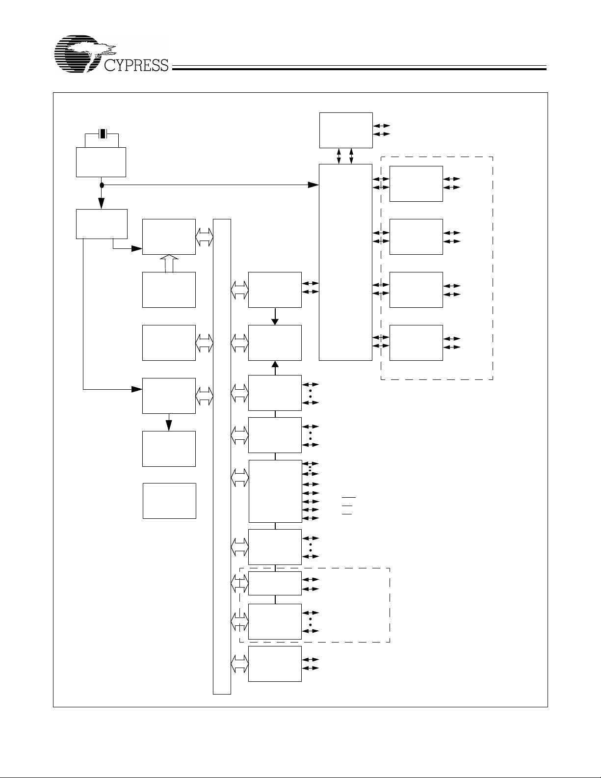
2.0 Functional Overview
The CY7C66013 and CY 7C66 113 are compound devices with a ful l-s pee d U SB mi cro co ntro lle r in c om bin ati on with a USB hub.
Each device is well suited for combination peripheral functions with hubs, such as a keyboard hub function. The 8-bit
one-time-programmable microcontroller with a 12-MBps USB Hub supports as many as 4 downstream ports.
The CY7C66013 feat ures 29 GP IO pins to s upport USB a nd other appli cations . The I/O pins are groupe d into four ports (P0[7:0 ],
P1[7:0], P2[7:0], P3[4:0]) where each port can be configured as inputs with internal pull-ups, open drain outputs, or traditional
CMOS outputs. Ports 0 to 2 are rated at 8 mA per pin (typical) sink current. Port 3 pins are rated at 12 mA per pin (typical) sink
current, which allows these pins to drive LEDs. Multiple GPIO pins can be connected together to drive a single output for more
drive current capac ity. Additio nal ly, eac h I /O pi n c an be us ed to g ene rate a GPIO interrupt to the micro co ntro lle r. All of the GPIO
interrupts all share the same “GPIO” interrupt vector.
The CY7C66113 has 31 GPIO p ins (P0 [7:0 ], P1 [7:0 ], P2 [7:0 ], P3 [6:0 ]). Additionally, the CY7C66113 featur es an ad diti ona l 8 I/O
pins in the Digital to Analog Conversion (DAC) port (P4[7:0] ). Every DAC pin includes an in tegrated 14-k Ω pull-up resistor. When
a ‘1’ is wr itten to a DAC I/O pin, th e output current sink is disabled a nd the output pin i s driven HIGH by the internal pull-up re sistor.
When a ‘0’ is written to a DAC I/ O pin, the internal p ull-up is disable d and the o utput pin p rovides the program med amount of sink
current. A DAC I/O pin can be used as an input with an internal pull-up by writing a ‘1’ to the pin.
The sink current for each DAC I/O pin can be individually programmed to one of sixteen values using dedicated Isink registers.
DAC bits DAC[1:0] can be used as high current outputs with a programmable sink current range of 3.2 to 16 mA (typical). DAC
bits DAC[7:2] have a programmable current sink range of 0.2 to 1.0 mA (typical). Multiple DAC pins can be connected together
to drive a single output that requires more sink current capacity. Each I/O pin can be used to generate a DAC interrupt to the
microcontroller. Also, the interrupt polarity for each DAC I/O pin is individually programmable.
The microcontroller uses an external 6-MHz crystal and an internal oscillator to provide a reference to an internal PLL-based
clock generator. This technology allow s the c ustom er appli cation to use an i nexpe nsive 6-MHz fundam ental crysta l that redu ce s
the clock-related noise emissions (EMI). A PLL clock generator provides the 6-, 12-, and 48-MHz clock signals for distribution
within the microcontroller.
The CY7C66013 and CY7C 66113 have 8 KB of PROM . These parts als o include Power-on Reset lo gic, a W atch Dog T imer, and
a 12-bit free-running timer. The Power-On Reset (POR) logic detects when power is applied to the device, resets the logic to a
known state, and begins executing instructions at PROM address 0x0000. The Watch Dog Timer is used to ensure the microcontroller recovers after a peri od of inac tiv ity. The firmw are may beco me inac tive for a va riety of reasons, including errors in the
code or a hardware failure such as waiting for an interrupt that never occurs.
2
The microcontroller can communicate with external electronics through the GPIO pins. An I
dates a 100-kHz serial link with an external device. There is also a Hardware Assisted Parallel Interface (HAPI) which can be
used to transfer data to an external device.
The free-running 12-bit timer clocked at 1 MHz provides two interrupt sources, 128-µs and 1.024-ms. The timer can be used to
measure the duration of an event under firmware control by reading the timer at the start of the event and after the event is
complete. The difference between the two readings indicates the duration of the event in microseconds. The upper four bits of
the timer are latched into a n internal register whe n the firmware reads the lower eight bits. A rea d from the upper four bits actually
reads data from the internal register, instead of the timer. This feature eliminates the need for firmware to try to compensate if
the upper four bits increment immediately after the lower eight bits are read.
The microcontroller su pports 11 m as kab le in terru pts in the vectored interrupt control ler. Interrupt s ou rces i nc lud e th e 1 28-µs (bit
6) and 1.024-ms (bit 9) outpu ts from the free-runn ing timer, five USB endpoints , the USB hub, the DAC po rt, the GPIO ports, an d
2
C-compatible master mode interface. The timer bits cause an interrupt (if enabled) when the bit toggles from LOW ‘0’ to
the I
HIGH ‘1.’ The USB en dpoints interrupt after the USB host h as written data to the endpoint FIFO or af ter the USB controlle r sends
a packet to the USB host. The DAC ports have an additional level of masking that allows the user to select which DAC inputs
can cause a DAC interrupt. Th e GPIO ports a lso have a level of m asking to select which GPIO inpu ts can cause a GPIO int errupt.
For additional flexibility, the input transition polarity that causes an interrupt is programmable for each pin of the DAC port. Input
transition polarity can be programmed for each GPIO port as part of the port configuration. The interrupt polarity can be rising
edge (‘0’ to ‘1’) or falling edge (‘1’ to ‘0’).
The CY7C66013 and CY7C66113 include an integrated USB Serial Interface Engine (SIE) that supports the integrated peripherals and the hub controller function. The hardware supports up to two USB device addresses with one device address for the
hub (two endpoints) and a dev ice address for a compound de vice (three endpoints). The SIE allows the USB host to communi cate
with the hub and functions integrated into the microcontroller. The part includes a 1:4 hub repeater with one upstream port and
four downstream po rts . Th e USB H ub al lows p ow er-management control of th e dow n stre am po rts by u si ng GPI O pin s as si gne d
by the user firmware. The user has the o ption of ganging t he downstre am ports together wi th a sing le pair o f power-mana gement
pins, or providing power management for each port with four pairs of power-management pins.
C-compatible interface accommo-
Document #: 38-08024 Rev. ** Page 7 of 53
Page 8
.
Logic Block Diagram
CY7C66013
CY7C66113
6-MHz crystal
PLL
48 MHz
Clock
Divider
12 MHz
6 MHz
12-MHz
8-bit
CPU
PROM
8 KB
RAM
256 byte
12-bit
Timer
8-bit Bus
USB
SIE
Interrupt
Controller
GPIO
PORT 0
USB
Transceiver
Repeater
P0[0]
P0[7]
D+[0]
Upstream
USB Port
D–[0]
USB
Transceiver
USB
Transceiver
USB
Transceiver
USB
Transceiver
Downstream USB Ports
Power management under firmware
control using GPIO pins
D+[1]
D–[1]
D+[2]
D–[2]
D+[3]
D–[3]
D+[4]
D–[4]
Watch Dog
Timer
Power-On
Reset
GPIO
PORT 1
GPIO/
HAPI
PORT 2
GPIO
PORT 3
GPIO
PORT 3
DAC
PORT
I2C
Interface
*I2C Compatible interface enabled by firmware through
P2[1:0] or P1[1:0]
P1[0]
P1[7]
P2[0:1,7]
P2[2]; Latch_Empty
P2[3]; Data_Ready
P2[4]; STB
P2[5]; OE
P2[6]; CS
P3[0]
P3[4]
P3[5]
P3[6]
DAC[0]
DAC[7]
CY7C66113 only
SCLK
SDATA
High Current
Outputs
Additional
High Current
Outputs
Document #: 38-08024 Rev. ** Page 8 of 53
Page 9

3.0 Pin Configurations
CY7C66013
CY7C66113
CY7C66013
48-pin PDIP/SSOP
REF
1
2
3
4
5
6
7
8
9
10
11
12
13
14
15
16
17
18
19
20
21
22
23
24
XTALOUT
XTALIN
V
P1[3]
P1[5]
P1[7]
P3[1]
D+[0]
D–[0]
P3[3]
GND
D+[1]
D–[1]
P2[1]
D+[2]
D–[2]
P2[3]
P2[5]
P2[7]
GND
P0[7]
P0[5]
P0[3]
P0[1]
TOP VIEW
CY7C66113
56-pin SSOP
48
V
CC
47
P1[1]
46
P1[0]
P1[2]
45
P1[4]
44
P1[6]
43
P3[0]
42
D–[3]
41
D+[3]
40
39
P3[2]
38
GND
37
P3[4]
D–[4]
36
35
D+[4]
34
P2[0]
33
P2[2]
32
GND
31
P2[4]
30
P2[6]
29
V
PP
P0[0]
28
P0[2]
27
P0[4]
26
25
P0[6]
XTALOUT
XTALIN
V
REF
P1[3]
P1[5]
P1[7]
P3[1]
D+[0]
D–[0]
P3[3]
GND
P3[5]
D+[1]
D–[1]
P2[1]
D+[2]
D–[2]
P2[3]
P2[5]
P2[7]
DAC[7]
P0[7]
P0[5]
P0[3]
P0[1]
DAC[5]
DAC[3]
DAC[1]
56
1
2
3
4
5
6
7
8
9
10
11
12
13
14
15
16
17
18
19
20
21
22
23
24
25
26
27
28
V
CC
55
P1[1]
54
P1[0]
P1[2]
53
P1[4]
52
P1[6]
51
P3[0]
50
D–[3]
49
48
D+[3]
47
P3[2]
46
P3[4]
45
D–[4]
D+[4]
44
43
P3[6]
42
P2[0]
41
P2[2]
GND
40
39
P2[4]
38
P2[6]
37
DAC[0]
V
36
PP
P0[0]
35
P0[2]
34
P0[4]
33
32
P0[6]
31
DAC[2]
30
DAC[4]
29
DAC[6]
Document #: 38-08024 Rev. ** Page 9 of 53
Page 10

4.0 Product Summary Tables
4.1 Pin Assignments
Table 4-1. Pin Assignments
Name I/O 48-Pin 56-Pin Description
D+[0], D–[0] I/O 8, 9 8, 9 Upstream port, USB differential data.
D+[1], D–[1] I/O 12, 13 13, 14 Downstream port 1, USB differential data.
D+[2], D–[2] I/O 15, 16 16, 17 Downstream port 2, USB differential data.
D+[3], D–[3] I/O 40, 41 48, 49 Downstream port 3, USB differential data.
D+[4], D–[4] I/O 35, 36 44, 45 Downstream port 4, USB differential data.
P0[7:0] I/O 21, 25, 22, 26,
P1[7:0] I/O 6, 43, 5, 44, 4,
P2[7:0] I/O 19, 30, 18, 31,
P3[6:0] I/O 37, 10, 39, 7, 4243, 12, 46,
DAC[7:0] I/O n/a 21, 29, 26,
XTAL
IN
XTAL
OUT
V
PP
V
CC
GND 11, 20, 32, 38 11, 40 Ground.
V
REF
OUT 1 1 6-MHz crystal out.
23, 27, 24, 28
45, 47, 46
17, 33, 14, 34
IN 2 2 6-MHz crystal or external clock input.
29 36 Programming voltage supply, tie to ground during normal operation.
48 56 Voltage supply.
IN 3 3 External 3.3V supply voltage for the differ ential data output buf fers and
22, 32, 23,
33, 24, 34,
25, 35
6, 51, 5, 52,
4, 53, 55, 54
20, 38, 19,
39, 18, 41,
15, 42
10, 47, 7, 50
30, 27, 31,
28, 37
GPIO Port 0.
GPIO Port 1.
GPIO Port 2.
GPIO Port 3, capable of sinking 12 mA (typical).
Digital to Analog Converter (DAC) Port with programmable current sink
outputs. DAC[1:0] offer a progra mmable range of 3.2 to 16 mA typ ical.
DAC[7:2] have a programmable sink current range of 0.2 to 1.0 mA
typical.
the D+ pull up.
CY7C66013
CY7C66113
4.2 I/O Register Summary
I/O registers are access ed via the I/O Read (IO RD) and I/O Wr ite (IOWR, IOWX) instr uctions. IORD read s data from the sele cted
port into the accum ulato r. IOWR performs the re verse; it write s dat a f rom th e accum ulator to the sele cted port. In dexed I/O W ri te
(IOWX) adds the con t en ts of X to th e address in the instructio n to form the port addres s and writes data from the ac cu mu lator to
the specified port. Specifying address 0 (e.g., IOWX 0h) means the I/O register is selected solely by the contents of X.
All undefined registers are reserved. It is important not to write to reserved registers as this may cause an undefined operation
or increased current consumption dur ing operati on. When writing to registers wit h reserved bits, the reserved bits mus t be written
with ‘0.’
Table 4-2. I/O Register Summary
Register Name I/O Address Read/Write Function Page
Port 0 Data 0x00 R/W GPIO Port 0 Data 19
Port 1 Data 0x01 R/W GPIO Port 1 Data 19
Port 2 Data 0x02 R/W GPIO Port 2 Data 19
Port 3 Data 0x03 R/W GPIO Port 3 Data 19
Port 0 Interrupt Enable 0x04 W Interrupt Enable for Pins in Port 0 20
Port 1 Interrupt Enable 0x05 W Interrupt Enable for Pins in Port 1 20
Port 2 Interrupt Enable 0x06 W Interrupt Enable for Pins in Port 2 20
Document #: 38-08024 Rev. ** Page 10 of 53
Page 11

CY7C66013
CY7C66113
Table 4-2. I/O Register Summary (continued)
Register Name I/O Address Read/Write Function Page
Port 3 Interrupt Enable 0x07 W Interrupt Enable for Pins in Port 3 20
GPIO Configuration 0x08 R/W GPIO Port Configurations 20
2
HAPI and I
USB Device Address A 0x10 R/W USB Device Address A 37
EP A0 Counter Register 0x11 R/W USB Address A, Endpoint 0 Counter 39
EP A0 Mode Register 0x12 R/W USB Address A, Endpoint 0 Configuration 38
EP A1 Counter Register 0x13 R/W USB Address A, Endpoint 1 Counter 39
EP A1 Mode Register 0x14 R/W USB Address A, Endpoint 1 Configuration 39
EP A2 Counter Register 0x15 R/W USB Address A, Endpoint 2 Counter 39
EP A2 Mode Register 0x16 R/W USB Address A, Endpoint 2 Configuration 39
USB Status & Control 0x1F R/W USB Upstream Port Traffic Status and Control 36
Global Interrupt Enable 0x20 R/W Global Interrupt Enable 27
Endpoint Interrupt Enable 0x21 R/W USB Endpoint Interrupt Enables 27
Interrupt Vector 0x23 R Pending Interrupt Vector Read/Clear 29
Timer (LSB) 0x24 R Lower 8 Bits of Free-running Timer (1 MHz) 22
Timer (MSB) 0x25 R Upper 4 Bits of Free-running Timer 22
WDT Clear 0x26 W Watch Dog Timer Clear 17
2
C Control & Status 0x28 R/W I2C Status and C ontrol 24
I
2
C Data 0x29 R/W I2C Data 24
I
DAC Data 0x30 R/W DAC Data 21
DAC Interrupt Enable 0x31 W Interrupt Enable for each DAC Pin 22
DAC Interrupt Polarity 0x32 W Interrupt Polarity for each DAC Pin 22
DAC Isink 0x38-0x3F W Input Sink Current Control for each DAC Pin 21
USB Device Address B 0x40 R/W USB Device Address B (not used in 5-endpoin t mode) 37
EP B0 Counter Register 0x41 R/W USB Address B, Endpoint 0 Counter 39
EP B0 Mode Register 0x42 R/W USB Address B, Endpoint 0 Configuration, or
EP B1 Counter Register 0x43 R/W USB Address B, Endpoint 1 Counter 39
EP B1 Mode Register 0x44 R/W USB Address B, Endpoint 1 Configuration, or
Hub Port Connect Status 0x48 R/W Hub Downstream Port Connect Status 33
Hub Port Enable 0x49 R/W Hub Downstream Ports Enable 34
Hub Port Speed 0x4A R/W Hub Downstream Ports Speed 34
Hub Port Control (Ports [4:1]) 0x4B R/W Hub Downstream Ports Control 34
Hub Port Suspend 0x4D R/W Hub Downstream Port Suspend Control 36
Hub Port Resume Status 0x4E R Hub Downstream Ports Resume Status 36
Hub Ports SE0 Status 0x4F R Hub Downstream Ports SE0 Status 35
Hub Ports Data 0x50 R Hub Downstream Ports Differential data 35
Hub Downstream Force Low 0x51 R/W Hub Downstream Ports Force LOW 35
Processor Status & Control 0xFF R/W Microprocessor Status and Control Register 26
C Configuration 0x09 R/W HAPI Width and I2C Position Configuration 23
USB Address A, Endpoint 3 in 5-endpoint mode
USB Address A, Endpoint 4 in 5-endpoint mode
38
39
Document #: 38-08024 Rev. ** P age 11 of 53
Page 12

CY7C66013
CY7C66113
4.3 Instruction Set Summary
Refer to the CYASM Assembler User’s Guide for more details.
Table 4-3. Instruction Set Summary
MNEMONIC operand opcode cycles MNEMONIC operand opcode cycles
HAL T 00 7 NOP 20 4
ADD A,expr data 01 4 INC A acc 21 4
ADD A,[expr] direct 02 6 INC X x 22 4
ADD A,[X+expr] index 03 7 INC [expr] direct 23 7
ADC A,expr data 04 4 INC [X+expr] index 24 8
ADC A,[expr] direct 05 6 DEC A acc 25 4
ADC A,[X+expr] index 06 7 DEC X x 26 4
SUB A,expr data 07 4 DEC [expr] direct 27 7
SUB A,[expr] direct 08 6 DEC [X+expr] index 28 8
SUB A,[X+expr] index 09 7 IORD expr address 29 5
SBB A,expr data 0A 4 IOWR expr address 2A 5
SBB A,[expr] direct 0B 6 POP A 2B 4
SBB A,[X+expr] index 0C 7 POP X 2C 4
OR A,expr data 0D 4 PUSH A 2D 5
OR A,[expr] direct 0E 6 PUSH X 2E 5
OR A,[X+expr] index 0F 7 SWAP A,X 2F 5
AND A,expr data 10 4 SWAP A,DSP 30 5
AND A,[expr] direct 11 6 MOV [expr],A direct 31 5
AND A,[X+expr] index 12 7 MOV [X+expr],A index 32 6
XOR A,expr data 13 4 OR [expr],A direct 33 7
XOR A,[expr] direct 14 6 OR [X+expr],A index 34 8
XOR A,[X+expr] index 15 7 AND [expr],A direct 35 7
CMP A,expr data 16 5 AND [X+expr],A index 36 8
CMP A,[expr] direct 17 7 XOR [expr],A direct 37 7
CMP A,[X+expr] index 18 8 XOR [X+expr],A index 38 8
MOV A,expr data 19 4 IOWX [X+expr] index 39 6
MOV A,[expr] direct 1A 5 CPL 3A 4
MOV A,[X+expr] index 1B 6 ASL 3B 4
MOV X,expr data 1C 4 ASR 3C 4
MOV X,[expr] direct 1D 5 RLC 3D 4
reserved 1E RRC 3E 4
XPAGE 1F 4 RET 3F 8
MOV A,X 40 4 DI 70 4
MOV X,A 41 4 EI 72 4
MOV PSP,A 60 4 RETI 73 8
CALL addr 50 - 5F 10 JC addr C0-CF 5
JMP addr 80-8F 5 JNC addr D0-DF 5
CALL addr 90-9F 10 JACC addr E0-EF 7
JZ addr A0-AF 5 INDEX addr F0-FF 14
JNZ addr B0-BF 5
Document #: 38-08024 Rev. ** Page 12 of 53
Page 13

CY7C66013
CY7C66113
5.0 Programming Model
5.1 14-Bit Program Counter (PC)
The 14-bit Program Counter (PC) allows acc es s to up to 8 KB of PROM avail abl e wi th the CY7C 66 x1 3 arch ite ctu re. The top 32
bytes of the ROM in the 8K part are reserved for testing purposes. The program counter is cleared during reset, such that the
first instruction e xe cut ed afte r a re se t is at add res s 0 x0 000 h. Typicall y, this is a ju mp in stru ction to a reset handler tha t initializes
the application (see Interrupt Vectors on page 28).
The lower eight bits of the program counter are incremented as instructions are loaded and executed. The upper six bits of the
program counter are increm ented by exe cuting an XPAGE instr uction . As a result, the la st instruc tion execu ted within a 256 -byte
“page” of sequential code should be an XPAGE instruction. The assembler directive “XPAGEON” causes the assembler to insert
XPAGE instructions automatically. Because instructions can be either one or two bytes long, the assembler may occasionally
need to insert a NOP followed by an XPAGE to execute correctly.
The address of the nex t inst ruction to be execu ted, the ca rry flag , and th e zero flag are save d as two bytes on the program sta ck
during an interrupt acknowledge or a CALL instruction. The program counter, carry flag, and zero flag are restored from the
program stack during a RETI instruction. Only the program counter is restored during a RET instruction.
The program counter cann ot be acc es se d di rec tly by t he fi rmwa re. Th e pro gram st ack ca n be examined by reading SRAM from
location 0x00 and up.
Document #: 38-08024 Rev. ** Page 13 of 53
Page 14

5.1.1 Program Memory Organization
after reset Address
14-bit PC 0x0000 Program execution begins here after a reset
CY7C66013
CY7C66113
0x0002 USB Bus Reset interrupt vector
0x0004 128-µs timer interrupt vector
0x0006 1.024-ms timer interrupt vector
0x0008 USB address A endpoint 0 interrupt vector
0x000A USB address A endpoint 1 interrupt vector
0x000C USB address A endpoint 2 interrupt vector
0x000E USB address B endpoint 0 interrupt vector
0x0010 USB address B endpoint 1 interrupt vector
0x0012 Hub interrupt vector
0x0014 DAC interrupt vector
0x0016 GPIO interrupt vector
0x0018
0x001A Program Memory begins here
0x1FDF 8 KB (-32) PROM ends here (CY7C66013, CY7C66113)
Figure 5-1. Program Memory Space with Interrupt Vector Table
I2C interrupt vector
5.2 8-Bit Accumulator (A)
The accumulator is the general-purpose register for the microcontroller.
5.3 8-Bit Temporary Register (X)
The “X” register is availa ble to the firmware for temporary storage of intermediate res ults. The microcontrol ler can perform inde xed
operations based on the value in X. Refer to Section 5.6.3 for additional information.
Document #: 38-08024 Rev. ** Page 14 of 53
Page 15
CY7C66013
CY7C66113
5.4 8-Bit Program Stack Pointer (PSP)
During a reset, the Program Stack Pointer (PSP) is set to 0x00 and “grows” upward from this address. The PSP may be set by
firmware, using the MOV PSP,A instruction. The PSP supports interrupt service under hardware control and CALL, RET, and
RETI instructions under firmware control. The PSP is not readable by the firmware.
During an interrupt acknowledge, interrupts are disabled and the 14-bit program counter, carry flag, and zero flag are written as
two bytes of data memory . The first byte is stored in the mem ory addressed by the PSP, then the PSP is incremented. The second
byte is stored in memory addressed by the PSP, and the PSP is incremented again. The overall effect is to store the program
counter and flags on the program “stack” and increment the PSP by two.
The Return From Interrup t (RETI) in struction decreme nts the PSP, then restores the second byte from memory a ddressed by the
PSP. The PSP is decrem ented again an d the first byte is restore d from memory addre ssed by the PSP. After the program counter
and flags have been res tored from stack, th e interrupts are enabled. The ov erall effe ct is to restore t he program counter a nd flags
from the program stack, decrement the PSP by two, and re-enable interrupts.
The Call Subroutine (CALL) instruction stores the program counter and flags on the program stack and increments the PSP by
two.
The Return From Subroutine (RET) instruction restores the program counter but not the flags from the program stack and
decrements the PSP by two.
5.4.1 Data Memory Organization
The CY7C66x13 microcontrollers provide 256 bytes of data RAM. Normally, the SRAM is partitioned into four areas: program
stack, user variab les, data s tack, and U SB endpoint FIFOs. The foll owing is one example o f where the program stack , data stack ,
and user variables areas could be located.
After reset Address
8-bit DSP 8-bit PSP 0x00 Program Stack Growth
(Move DSP
8-bit DSP
[1]
)
user selected Data Stack Growth
User variables
USB FIFO space for up to two Addre sses and five endpo ints
0xFF
[2]
5.5 8-Bit Data Stack Pointer (DSP)
The Data Stack Pointer (DSP) supports PUSH and POP instructions that use the data stack for temporary storage. A PUSH
instruction pre-decrements the DSP, then writes data to the memory location addressed by the DSP. A POP instruction reads
data from the memory location addressed by the DSP, then post-increments the DSP.
During a reset, the DSP is reset to 0x00. A PUSH instruction when DSP equals 0x00 writes data at the top of the data RAM
(address 0xFF). This writes data to the memory area reserved for USB endpoint FIFOs. Therefore, the DSP should be indexed
at an appropriate memory location that does not compromise the Program Stack, user-defined memory (variables), or the USB
endpoint FIFOs.
For USB applications , the firmw are shou ld set the DSP to a n appropriate location to avoid a memo ry confli ct with RAM dedic ated
to USB FIFOs. The memory requirements for the USB endpoints are described in Section 19.2. Example assembly instructions
to do this with two device addresses (FIFOs begin at 0xD8) are shown below:
MOV A,20h ; Move 20 hex into Accumulator (must be D8h or less)
SWAP A,DSP ; swap accumulator value into DSP register
Notes:
1. Refer to Section 5.5 for a description of DSP.
2. Endpoint sizes are fixed by the Endpoint Size Bit (I/O register 0x1F, Bit 7), see Table 19-1.
Document #: 38-08024 Rev. ** Page 15 of 53
Page 16
CY7C66013
CY7C66113
5.6 Address Modes
The CY7C66013 and CY7C66113 microcontrollers support three addressing modes for instructions that require data operands:
data, direct, and indexed.
5.6.1 Data (Immediate)
“Data” address mode refers to a data operan d that is actually a con stant encoded in the instruct ion. As an example, co nsider the
instruction that loads A with the constant 0xD8:
• MOV A,0D8h
This instruction requires two bytes of code where the first byte identifies the “MOV A” instruction with a data operand as the
second byte. The second byte of the instruction is the constant “0xD8”. A constant may be refe r red to by na me if a pr ior “EQU”
statement assigns the constant value to the name. For example, the following code is equivalent to the example shown above:
• DSPINIT: EQU 0D8h
• MOV A,DSPINIT
5.6.2 Direct
“Direct” address mode is used when the data operand is a variable stored in SRAM. In that case, the one byte address of the
variable is encoded in the instruction. As an example, consider an instruction that loads A with the contents of memory address
location 0x10:
• MOV A,[10h]
Normally, variable names are assigned to variable addresses using “EQU” statements to imp rove the rea dability of the assembl er
source code. As an example, the following code is equivalent to the example shown above:
• buttons: EQU 10h
• MOV A,[buttons]
5.6.3 Indexed
“Indexed” address mode allows the firmware to manipulate arrays of data stored in SRAM. The address of the data operand is
the sum of a constant e ncoded in the instructio n and the c ontents of t he “X” registe r . Normal ly, the constant is the “base” address
of an array of data and the X register contains an index that indicates which element of the array is actually addressed:
• array: EQU 10h
• MOV X,3
• MOV A,[X+array]
This would have the effect of loading A with the fourth element of the SRAM “array” that begins at address 0x10. The fourth
element would be at address 0x13.
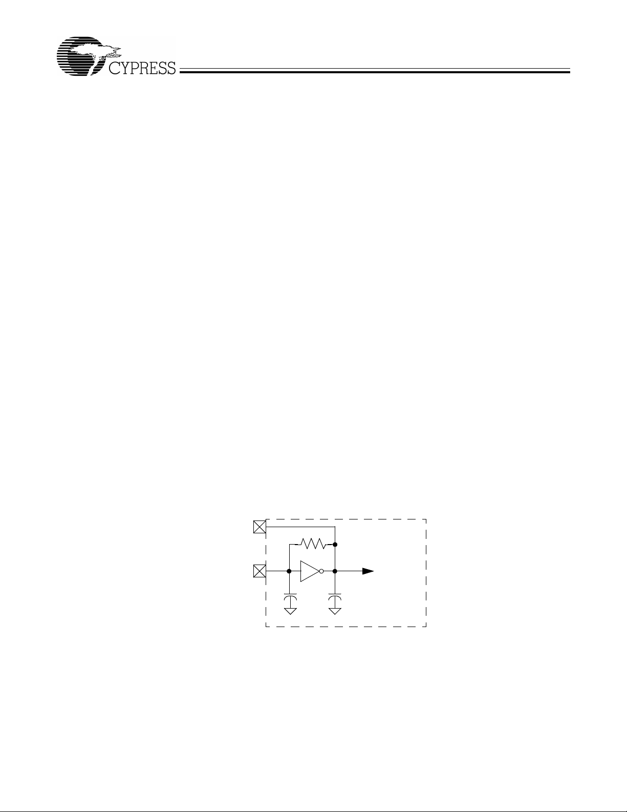
6.0 Clocking
XTALOUT
(pin 1)
XTALIN
(pin 2)
30 pF
Figure 6-1. Clock Oscillator On-Chip Circuit
The XTALIN and XTALOUT are the clock pins to the microcontroller. The user can connect an external oscillator or a crystal to
these pins. When using an ex tern al c rys tal , kee p PC B traces be tw een the ch ip le ads and crys tal as sh ort as pos sible (less than
2 cm). A 6-MHz fundamenta l frequency p arallel resonant crystal can be connecte d to these pin s to provide a reference fre quency
for the internal PLL. Th e two inte rnal 30 -pF load caps appear i n series t o the ex ternal c rystal an d wou ld be e quiva lent to a 15-pF
load. Therefore, the crystal must have a required load capacitance of about 15–18 pF. A ceramic resonator does not allow the
microcontroller to meet the timing specifications of full speed USB and therefore a ceramic resonator is not recommended with
these parts.
An external 6-MHz clock can be applied to the XTALIN pin if the XTALOUT pin is left open. Grounding the XTALOUT pin when
driving XTALIN with an oscillator does not work because the internal clock is effectively shorted to ground.
to internal PLL
30 pF
Document #: 38-08024 Rev. ** Page 16 of 53
Page 17

CY7C66013
CY7C66113
7.0 Reset
The CY7C66x13 supports two resets: Power-On Reset (POR) and a Watch Dog Reset (WDR). Each of these resets causes:
• all registers to be restored to their default states,
• the USB Device Addresses to be set to 0,
• all interrupts to be disabled,
• the PSP and Data Stack Pointer (DSP) to be set to memory address 0x00.
The occurrence of a reset is recorded in the Processor Status and Control Register, as described in Section 15.0. Bits 4 and 6
are used to record the occurr ence of POR and WDR resp ectivel y. Firmware can int errogate these bit s to determ ine the ca use of
a reset.
Program execution starts at ROM address 0x0000 after a reset. Although this looks like interrupt vector 0, there is an important
difference. Reset processing does NOT push the program counter, carry flag, and zero flag onto program stack. The firmware
reset handler should configure the hardware before the “main” loop of code. Attem pting to execute a R ET or RETI in the firmwa re
reset handler causes unpredictable execution results.
7.1 Power-On Reset (POR)
When VCC is first applied to the chi p, the Power-On Reset (POR) signa l is asserted and th e CY7C66x13 e nters a “semi-suspend”
state. During the semi-suspend state, which is different from the suspend state defined in the USB specification, the oscillator
and all other block s o f th e part are functional, exc ept for the CPU. This semi-susp end tim e ens ure s that both a valid V
reached and tha t the inte rnal PLL has tim e to sta bilize befo re full o peratio n begins. When t he V
2.5V, and the oscillator is stable, the POR is deasserted and the on-chip timer starts counting. The first 1 ms of suspend time is
not interruptible, a nd the semi -suspend sta te continues fo r an additiona l 95 ms unl ess the coun t is bypassed by a USB Bus Res et
on the upstream port. The 95 ms provides time for V
If a USB Bus Reset occurs on the upstream port during the 95 ms semi-suspend time, the semi-suspend state is aborted and
program execution begins immediately from address 0x0000. In this case, the Bus Reset interrupt is pending but not serviced
until firmware sets the USB Bus Reset Interrupt Enable bit (bit 0 of register 0x20) and enables interrupts with the EI command.
The POR signal is asserte d whenever V
again. Behavior is the same as described above.
drops below approxim ately 2.5V , an d remains asserte d until VCC rises above this leve l
CC
to stabilize at a valid operating voltage before the chip executes code.
CC
has risen above approxi mately
CC
level is
CC
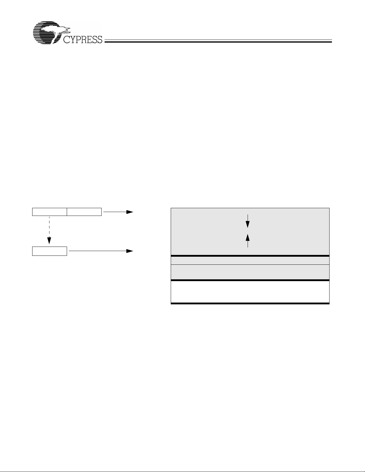
7.2 Watch Dog Reset (WDR)
The Watch Dog Timer Reset (WDR) occurs when the internal Watch Dog Timer rolls over. Writing any value to the write-only
Watch Dog Restart Register at address 0x26 clears the timer. The timer rolls over and WDR occurs if it is not cleared within
(8 ms minimum) of the la st clear . Bit 6 of th e Processor Statu s and Control Regis ter is set to reco rd this event (th e register
t
WATCH
contents are set to 010X0001 by the WDR). A Watch Dog Timer Reset lasts for 2 ms, after which the microcontroller begins
execution at ROM address 0x0000.
t
WATCH
Last write to
Watch Dog Timer
Register
The USB transmitter is disabled by a Watch Dog Reset because the USB Device Address Registers are cleared (see Section
19.1). Otherwise, the USB Controller would respond to all address 0 transactions.
It is possible for the WDR bit of the Proc ess or St atus an d Control Register (0xFF) to be se t foll owin g a PO R ev ent . If a fi rmw a re
interrogates the Processor Statu s and Cont rol Regis ter for a set condi tion on the WDR bit, the WDR bit should be ignored if the
POR (bit 3 of register 0xFF) bit is set.
No write to WDT
register, so WDR
goes HIGH
Figure 7-1. Watch Dog Reset (WDR)
2 ms
Execution begins at
Reset Vector 0x0000
Document #: 38-08024 Rev. ** Page 17 of 53
Page 18

CY7C66013
CY7C66113
8.0 Suspend Mode
The CY7C66x13 can be placed into a low-power state by setting the Suspend bit of the Processor Status and Control register.
All logic blocks in the device are turned off except the GPIO interrupt logic and the USB receiver. The clock oscillator and PLL,
as well as the free-running and watch dog timers, are shut down. Only the occurrence of an enabled GPIO interrupt or non-idle
bus activity at a USB upst ream or downstream p ort wakes the part from sus pend. The Run bit in th e Processor Status and Control
Register must be set to resume a part out of suspend.
The clock oscillator restarts immediately after exiting suspend mode. The microcontroller returns to a fully functional state 1 ms
after the oscillator is stable. The microcon troller executes the inst ruction following th e I/O write that placed the device into suspen d
mode before servicing any interrupt requests.
The GPIO interrupt allows the controller to wake-up periodic ally and poll system componen ts while maintaining a very low av erage
power consumption. To achieve the lowest possi ble current d uring suspend mode, all I/O shoul d be held at V
applies to internal port pins that may not be bonded in a particular package.
Typical code for entering suspend is shown below:
... ; All GPIO set to low-power state (no floating pins)
... ; Enable GPIO interrupts if desired for wake-up
mov a, 09h ; Set suspend and run bits
iowr FFh ; Write to Status and Control Register - Enter suspend, wait for USB activity (or GPIO Interrupt)
nop ; This executes before any ISR
... ; Remaining code for exiting suspend routine
or Gnd. This also
CC
9.0 General-Purpose I/O (GPIO) Ports
GPIO
CFG
OE
Internal
Data Bus
Port Write
Port Read
Reg_Bit
STRB
(Latch is Transparent
except in HAPI mode)
Interrupt
Enable
Interrupt
Controller
Data
Out
Latch
Data
In
Latch
Data
Interrupt
Latch
mode
2-bits
Control
Control
V
CC
Q1
14 kΩ
Q3*
Q2
*Port 0,1,2: Low I
Port 3: High I
sink
GPIO
PIN
sink
Figure 9-1. Block Diagram of a GPIO Pin
There are up to 31 GPIO pins (P0[7:0], P1[7:0], P2[7:0], and P3[6:0]) for the hardware interface. The number of GPIO pins
changes based on th e package type of the ch ip. Each port c an be confi gured as inp uts with intern al pull-up s, open drain outputs ,
or traditional CMOS outputs. Port 3 offers a higher current drive, with typical current sink capability of 12 mA. The data for each
GPIO port is accessible through the data registers. Port data registers are shown in Figure 9-2 through Figure 9-5, and are set
to 1 on reset.
Document #: 38-08024 Rev. ** Page 18 of 53
Page 19

CY7C66013
CY7C66113
7 6 5 4 3 2 1 0
P0[7] P0[6] P0[5] P0[4] P0[3] P0[2] P0[1] P0[0]
Figure 9-2. Port 0 Data 0x00 (read/write)
7 6 5 4 3 2 1 0
P1[7] P1[6] P1[5] P1[4] P1[3] P1[2] P1[1] P1[0]
Figure 9-3. Port 1 Data 0x01 (read/write)
7 6 5 4 3 2 1 0
P2[7] P2[6] P2[5] P2[4] P2[3] P2[2] P2[1] P2[0]
Figure 9-4. Port 2 Data 0x02 (read/write)
7 6 5 4 3 2 1 0
P3[7]
(see text)
P3[6] P3[5] P3[4] P3[3] P3[2] P3[1] P3[0]
Figure 9-5. Port 3 Data 0x03 (read/write)
Special care sho uld be ta ken w ith a ny un used GPIO data bits . An unu sed G PIO d ata bit , eithe r a pin on the c hip o r a port bit th at
is not bonded on a particular package, must not be left floating when the device enters the suspend state. If a GPIO data bit is
left floating, the leakage current caused by the floating bit may violate the suspend current limitation specified by the USB
specifications. If a ‘1’ is written to the unused data bit and the port is configured with open drain outputs, the unused data bit
remains in an indeterminate state. Therefore, if an unused port bit is programmed in open-drain mode, it must be written with a
‘0.’ Notice that the CY7C66 013 al ways req uires th at P3[7:5 ] be written with a ‘0.’ When the CY7C66113 is used the P3[7] should
be written with a ‘0.’
In normal non-HAPI mode, reads from a GPIO port always return the present state of the voltage at the pin, independent of the
settings in the Port Data Registers. If HAPI mode is activated for a port, reads of that port return latched data as controlled by
the HAPI signals (see Section 14.0). During reset, all of the GPIO pins are set to a high impedance input state (‘1’ in ope n drai n
mode). Writi ng a ‘0’ to a GPIO pin drives the pin LOW. In this state, a ‘0’ is always rea d on that GPI O pin unless an external
source overdrives the internal pull-down device.
9.1 GPIO Configuration Port
Every GPIO port can be programmed as inputs with internal pull-ups, open drain outputs, and traditional CMOS outputs. In
addition, the interrupt polarity for each port can be programmed. With positive interrupt polarity, a rising edge (‘0’ to ‘1’) on an
input pin causes an interrup t. With n egativ e pola rity, a falli ng edge (‘1’ to ‘0’) on an inpu t pin c auses an int errupt. As sh own i n the
table below, when a GPIO po rt i s con figured with CMOS outputs, inte rrup ts from th at p ort are disabled. The GPIO Co nfi gura tio n
Port register provides two bits per port to program these features. The possible port configurations are detailed in Table 9-1:
Table 9-1. Port Configurations
Port Configuration bits Pin Interrupt Bit Driver Mode Interrupt Polarity
11 0 Resistive Disabled
1Resistive–
10 0 CMOS Output Disabled
1 Open Drain Disabled
01 0 Open Drain Disabled
1 Open Drain –
00
(Reset Stat e)
0 Open Drain Disabled (Default Condition)
1 Open Drain +
In “Resistive” mode, a 14-kΩ pull-up resistor is conditionally enable d for all pins of a GPIO port. An I/O pin is dri ven HIGH throug h
a 14-kΩ pull-up resistor when a ‘1’ ha s b een w rit ten to the pin. The output pin is driven LOW w ith the pu ll-up disabled when a ‘0’
has been written to the pi n. An I/O pin that has be en written as a ‘1’ can be used as an input pin with the integr ated 14-kΩ pull-u p
resistor. Resistive mode selects a negative (falling edge) interrupt polarity on all pins that have the GPIO interrupt enabled.
Document #: 38-08024 Rev. ** Page 19 of 53
Page 20

CY7C66013
CY7C66113
In “CMOS” mode, all pins of the GPIO port are outp uts that are ac tively driven. A C MOS port is no t a possible sou rce for interrupts .
In “Open Drain” mode, the internal pull-up resistor and CMOS driver (HIGH) are both disabled. An open drain I/O pin that has
been written as a ‘1’ can be used as an input or an open drain output. An I/O pin that has been written as a ‘0’ drives the output
low. The interrupt polarity for an open drain GPIO port can be selected as positive (rising edge) or negative (falling edge).
During reset, all of the bits in the GPIO Configuration Register are written with ‘0’ to select Open Drain output for all GPIO ports
as the default configuration.
7 6 5 4 3 2 1 0
Port 3
Config Bit 1
9.2 GPIO Interrupt Enable Ports
Each GPIO pin can be individually enabled or disabled as an interrupt source. The Port 0–3 Interrupt Enable registers provide
this feature with an interrupt enable bit for each GPIO pin. When HAPI mode (discussed in Section 14.0) is enabled the GPIO
interrupts are blocked, including ports not used by HAPI, so GPIO pins cannot be used as interrupt sources.
During a reset, GPIO interrupts are disabled by clearing all of the GPIO interrupt enable ports. Writing a ‘1’ to a GPIO Interrupt
Enable bit enables GPIO interrupts from the corresponding input pin. All GPIO pins share a common interrupt, as discussed in
Section 16.8.
Port 3
Config Bit 0
Port 2
Config Bit 1
Figure 9-6. GPIO Configuration Register 0x08 (read/write)
Port 2
Config Bit 0
Port 1
Config Bit 1
Port 1
Config Bit 0
Port 0
Config Bit 1
Port 0
Config Bit 0
7 6 5 4 3 2 1 0
P0[7] P0[6] P0[5] P0[4] P0[3] P0[2] P0[1] P0[0]
Figure 9-7. Port 0 Interrupt Enable 0x04 (write only)
7 6 5 4 3 2 1 0
P1[7] P1[6] P1[5] P1[4] P1[3] P1[2] P1[1] P1[0]
Figure 9-8. Port 1 Interrupt Enable 0x05 (write only)
7 6 5 4 3 2 1 0
P2[7] P2[6] P2[5] P2[4] P2[3] P2[2] P2[1] P2[0]
Figure 9-9. Port 2 Interrupt Enable 0x06 (write only)
7 6 5 4 3 2 1 0
reserved set to zero
P3[6] P3[5] P3[4] P3[3] P3[2] P3[1] P3[0]
Figure 9-10. Port 3 Interrupt Enable 0x07 (write only)
Document #: 38-08024 Rev. ** Page 20 of 53
Page 21

10.0 DAC Port
CY7C66013
CY7C66113
V
CC
Internal
Data Bus
Data
Out
Latch
DAC Write
Suspend
(Bit 3 of Register 0xFF)
Q1
14 kΩ
DAC
I/O Pin
4 bits
Isink
DAC
to Interrupt
Controller
Interrupt
Enable
Interrupt
Polarity
Internal
Buffer
DAC Read
Isink
Register
Interrupt Logic
Figure 10-1. Block Diagram of a DAC Pin
The CY7C661 13 feat ures a Digital to An alog Conversion (DAC) p ort which has prog rammable current sink on each I/O pin. Writing
a ‘1’ to a DAC I/O pin disables the output current sink (Isink DAC) and drives the I/O pin HIGH through an integrated 14-kΩ
resistor . When a ‘0’ is wr itten to a DAC I/O pin, th e Isink DAC is e nabled an d the pul l-up resi stor is d isabled. This ca uses the Isink
DAC to sink current to drive the output LOW. The amount of sink current for the DAC I/O pin is programmable over 16 values
based on the contents of the DAC Isink Register for that output pin. DAC[1:0] are high current outputs that are programmable
from 3.2 mA to 16 mA (typical). DAC[7:2] are low current outputs, programmable from 0.2 mA to 1.0 mA (typical).
When the suspend bit in Proces sor Status and Control Reg ister (0xFF) is set, the Isink D AC block of the DAC circuitry is disabled.
Special care should be t aken w he n the C Y7C 64 x1 3 dev ic e is pl ac ed in the sus pe nd. T he DA C Port D a ta R eg ist er(0 x30 ) sh oul d
normally be loaded with all ‘1’s (0xFF) before setting the suspend bit. If any of the DAC bits are set to ‘0’ when the device is
suspended, th at DAC input wil l float. The fl oating pin coul d result in exce ssive curre nt consumptio n by the device, unless an
external load places the pin in a deterministic state.
When a DAC I/O bit is writt en as a ‘1’, th e I/O pin is an outpu t pulle d HIGH through the 14-kΩ res istor or an input with an interna l
14-kΩ pull-up resistor. All DAC port data bits are set to ‘1’ during reset.
Low current outputs
0.2 mA to 1.0 mA typical
High current outputs
3.2 mA to 16 mA typical
7 6 5 4 3 2 1 0
DAC[7] DAC[6] DAC[5] DAC[4] DAC[3] DAC[2] DAC[1] DAC[0]
Figure 10-2. DAC Port Data 0x30 (read/write)
10.1 DAC Isink Registers
Each DAC I/O pin has an associated DAC Isink register to program the output sink current when the output is driven LOW. The
first Isink register (0x38 ) con trol s th e cu rrent for DA C[0], the second (0x39) for DAC[1], and so on unti l the Isi nk regis ter at 0x3 F
controls the current to D AC[7]. Writing all ‘0’s to the Isink register ca us es 1/5 of the max current to flow through the DAC I /O pin.
Writing all ‘1’s to the Isink register provide s the maximum current flow through the pin. The other 14 st ates of the DAC sink current
are evenly spaced between the se tw o val ues.
Isink Value
7 6 5 4 3 2 1 0
reserved reserved reserved reserved Isink[3] Isink[2] Isink[1] Isink[0]
Figure 10-3. DAC Port Isink 0x38 to 0x3F (write only)
Document #: 38-08024 Rev. ** Page 21 of 53
Page 22

CY7C66013
CY7C66113
10.2 DAC Port Interrupts
A DAC port interrupt can be enabled/disabled for each pin individually. The DAC Port Interrupt Enable register provides this
feature with an interrupt enable bit for each DAC I/O pin. Writing a ‘1’ to a bit in this register enables interrupts from the corresponding bit po sition . W riti ng a ‘0’ to a bit in the DAC Port Int errup t Enabl e regi ster di sable s int errupts from th e corre spond ing b it
position. All of th e DAC Port In terrupt Enable register bi ts are cleared to ‘0’ during a reset. Al l DAC pins share a com mon interrup t,
as explained in Section 16.7.
7 6 5 4 3 2 1 0
DAC[7] DAC[6] DAC[5] DAC[4] DAC[3] DAC[2] DAC[1] DAC[0]
Figure 10-4. DAC Port Interrupt Enable 0x31 (write only)
As an additional benefit, the interrupt polarity for each DAC pin is programmable with the DAC Port Interrupt Polarity register.
Writing a ‘0’ to a bit selects negative polarity (falling edge) that causes an interrupt (if enabled) if a falling edge transition occurs
on the correspond ing in put pin . Writing a ‘1’ to a bit i n th is reg is ter s el ec ts pos iti ve po lari ty (ris ing ed ge) that causes an interrupt
(if enabled) if a rising edge transition occurs on the corresponding input pin. All of the DAC Port Interrupt Polarity register bits
are cleared during a reset.
7 6 5 4 3 2 1 0
DAC[7] DAC[6] DAC[5] DAC[4] DAC[3] DAC[2] DAC[1] DAC[0]
Figure 10-5. DAC Port Interrupt Polarity 0x32 (write only)
11.0 12-Bit Free-Running Timer
The 12-bit timer provides two interrupts (128-µs and 1.024-ms) and allows the firmware to directly time events that are up to
4 ms in duration. The lower 8 bits of the timer can be read directly by the firmware. Reading the lower 8 bits latches the upper
4 bits into a temporary register. When the firmware reads the upper 4 bits of the timer, it is accessing the count stored in the
temporary register. The eff ect of this logic is to ensure a stable 12-bit tim er value can be re ad, even wh en the tw o reads ar e
separated in time.
11.1 Timer (LSB)
7 6 5 4 3 2 1 0
Timer
Bit 7
11.2 Timer (MSB)
7 6 5 4 3 2 1 0
Reserved Reserved Reserved Reserved Timer
Timer
Bit 6
Timer
Bit 5
Figure 11-1. Timer Register 0x24 (read only)
Figure 11-2. Timer Register 0x25 (read only)
Timer
Bit 4
Timer
Bit 3
Bit 11
Timer
Bit 2
Timer
Bit 10
Timer
Bit 1
Timer
Bit 9
Timer
Bit 0
Timer
Bit 8
Document #: 38-08024 Rev. ** Page 22 of 53
Page 23

CY7C66013
CY7C66113
1.024-ms Interrupt
128-
µs Interrupt
10 9 7856432
1 011
1-MHz Clock
L1 L0L2L3
D3 D2 D1 D0 D7 D6 D5 D4 D3 D2 D1 D0
To Timer Register
8
Figure 11-3. Timer Block Diagram
12.0 I2C and HAPI Configuration Register
Internal hardware suppo rts c om mu nic ati on with ex tern al de vi ce s through two interfaces: a two-wire I2C compatible, and a HAPI
for 1, 2, or 3 byte tra nsfers. The I
configuration registe r (see Figure 12-1 ). All bits of this register are cleared on reset.
7 6 5 4 3 2 1 0
R/W R/W R/W R R R/W R/W
I2C Position Reserved LEMPTY
Bits [7,1:0] of the HAPI/I
Bits [5:2] are used in HAPI mode only, and are described in Section 14.0. Table 12-1 shows the HAPI port configurations, and
Table 12-2 shows I
packages, and to allow simultaneous HAPI and I2C compatible operation.
HAPI operation is enabled whenever e ither HAP I Port W idth Bit ( Bit 1 or 0 ) is non -zero. Thi s af fects G PIO opera tion as describe d
in Section 14.0. The I
Table 12-1. HAPI Port Configuration
Table 12-2. I
I2C Position
2
C pin location configuration options. These I2C compatible options exist due to pin limitations in certain
2
C-compatible interface must be separately enabled as described in Section 13.0.
Port Width
Bits[1:0] HAPI Port Width
11 24 Bits: P3[7:0], P1[7:0], P0[7:0]
10 16 Bits: P1[7:0], P0[7:0]
01 8 Bits: P0[7:0]
00 No HAPI Interface
2
C Port Configuration
Bit[7]
X1I
00I
10I
2
C compatible and H API functions, dis cussed in detai l in Sections 13. 0 and 14.0, share a common
Polarity
Figure 12-1. HAPI/I2C Configuration Register 0x09 (read/write)
2
C Configuration Register control the pin out configuration of the HAPI and I2C compatible interfaces.
Port Width
DRDY
Polarity
Bit[1] I2C Positio n
Latch Empty Data Ready HAPI Port
2
C on P2[1:0], 0:SCL, 1:SDA
2
C on P1[1:0], 0:SCL, 1:SDA
2
C on P2[1:0], 0:SCL, 1:SDA
Width Bit 1
HAPI Port
Width Bit 0
Document #: 38-08024 Rev. ** Page 23 of 53
Page 24
13.0 I2C Compatible Controller
CY7C66013
CY7C66113
The I2C-compatible block provides a versatile two-wire communication with external devices, supporting master, slave, and
multi-master modes of operat ion. The I
interrupts as needed to allow firmware to take appropriate action during transactions. While waiting for firmware response, the
hardware keeps the I
2
C-compatible interface generates an interrupt to th e m ic roc ontr oll er at the end of each received or tra nsmi tted byte, when
The I
2
C-compatible bus idle if neces sar y.
2
C-compatible blo ck functio ns by handl ing the low- level sig naling in h ardware, and i ssuing
a stop bit is detected by the slave when in receive mode, or when arbitration is lost. Details of the interrupt responses are given
in Section 16.9.
2
C-compatible interfac e consists of two registers , an I2C Data Register (Figure 13-1) and an I2C Status and Control Register
The I
(Figure 13-2). The Data Register is implemented as separate read and write registers. Generally, the I
Register should only be monitored afte r the I
2
C interrupt, as all bits are valid at that time. Polling thi s register at oth er times could
2
C Status and Control
read misleading bit status if a transaction is underway.
2
C SCL clock is connected to bit 0 of GPIO port 1 or GPIO port 2, and the I2C SDA data is connected to bit 1 of GPIO port
The I
1 or GPIO port 2. Refer to Section 12.0 for the bit definitions and functionality of the HAPI/I2C Configuration Register, which is
used to set the locations of the co nfigurable I
Status & Control Register, the two LSB ([1:0]) of the corresponding GPIO port is placed in Open Drain mode, regardless of the
settings of the GPIO Configuration Register.The electrical characteristics of the I
GPIO ports 1 and 2. Note that the I
OL
2
C pins. Once the I2C-compatible func tio na lity is ena ble d by sett ing bit 0 of the I2C
(max) is 2 mA @ V
= 2.0V for ports 1 and 2.
OL
2
C-compatible interface is the same as that of
All control of the I2C clock and data lines is performed by the I2C compatible block.
7 6 5 4 3 2 1 0
I2C Data 7 I2C Data 6 I2C Data 5 I2C Data 4 I2C Data 3 I2C Data 2 I2C Data 1 I2C Data 0
Figure 13-1. I2C Data Register 0x29 (separate read/write registers)
7 6 5 4 3 2 1 0
R/W R/W R/W R/W R/W R/W R/W R/W
MSTR
Mode
Continue/
Busy
Xmit
Mode
ACK Addr ARB Lost/
Restart
Received
Stop
I2C
Enable
Figure 13-2. I2C Status and Control Register 0x28 (read/write)
The I2C Status and Control register bits are defined in Table 13-1, with a more detailed description following.
Table 13-1. I
2
C Status and Control Register Bit Definitions
Bit Name Description
0I2C Enable Write to 1 to enable I2C-compatible function. When cleared, I2C GPIO pins operate
normally.
2
1 Received Stop Reads 1 only in slave re ceive mod e, when I
C Stop bit detected (unless firmw are did not
ACK the last transaction).
2 ARB Lost/Restart Reads 1 to indicate master has lost arbitration. Reads 0 otherwise.
Write to 1 in master mode to perform a restart sequence (also set Continue bit).
3 Addr Reads 1 during first byte after start/restart in slave mode, or if master loses arbitration.
Reads 0 otherwise. This bit should always be written as 0.
4 ACK In receive mode, write 1 to generate ACK, 0 for no ACK.
In transmit mode, reads 1 if ACK was received, 0 if no ACK received.
5 Xmit Mode Write to 1 for transmit mode, 0 for receive mode.
6 Continue/Busy Write 1 to indicate ready for next transaction.
Reads 1 when I
2
C-compatible block is busy with a transaction, 0 when transaction is
complete.
7 MSTR Mode Write to 1 for master mode, 0 for slave mo de. This bit is cleared if maste r loses arbitration.
Clearing from 1 to 0 generates Stop bit.
Document #: 38-08024 Rev. ** Page 24 of 53
Page 25

CY7C66013
CY7C66113
MSTR Mode: Setting this bit c au ses th e I2C to initiate a master m ode trans ac ti on b y s end ing a st art bit and transmitting the first
data byte from the data register (this typically holds the target address and R/W bit). Subsequent bytes are initiated by setting
the Continue bit, as described below.
2
In master mode, th e I
or receive sta te. The I2C-compatible block performs any required arbitration and clock synchronization. The loss of arbitration
results in the clearing of this bit, the setting of the ARB Lost bit, and the generation of an interrupt to the microcontroller. If the
chip is the target of an external master that wins arbitration, then the interrupt is held off until the transaction from the external
master is completed.
When MSTR Mode is cleared from 1 to 0 by a firmware write, an I
Continue/Busy: This bit i s wri tten by t he firm ware to indicate that the firmware is rea dy for the ne xt byte transaction to b egi n. In
other words, the bit has responded to an interrupt request and has completed the required update or read of the data register.
During a read this bit indicates if the hardware is busy and is locking out additional writes to the I
This locking allows the hardware to complete certain operations that may require an extended period of time. Following an I
interrupt, the I
2
to make one control register write without the need to check the Busy bit.
Xmit Mode: This bit is set by firmware to enter transmit mode and perform a data transmit in master or slave mode. Clear this
bit for receive mode. Firmware ge nerally determi nes the value of thi s bit from the R/W bit asso ciated with the I
The Xmit Mode bit state is ignore d when initially writi ng the MSTR Mode or the Resta rt bits, as these cases alway s cause transmit
mode for the first byte.
ACK: This bit is set or cleared by firmware during receive operation to indicate if the hardware should generate an ACK signal
2
on the I
C-compatible bus. Writing a 1 to this bit generates an ACK (SDA LOW) on the I2C-compatible bus at the ACK bit time.
During transmits (Xmit Mode = 1), this bit should be cleared.
Addr: This bit is se t by th e I
The Addr bit is cleared when the firmware sets the Continue bit. This bit allows the firmware to recognize when the master has
lost arbitration, and in slave mode it allows the firmware to recognize that a start or restart has occurred.
ARB Lost/Restart: This bit is valid as a status bit (ARB Los t) after master mode tran sactions . In master mode , set this bit (alon g
with the Continue and MSTR Mo de bits) to perform an I
to the data register before setting the Continue bit. To prevent false ARB Lost signals, the Restart bit is cleared by hardware
during the restart sequ ence.
Receive Stop: This bit is se t when the slave is in rec eive mode and detects a stop bit on the bus. The Receive Stop bit is not set
if the firmware t erminates the I
in receive mode if firmware sets the Continue bit and clears the ACK bit.
2
C Enable: Set this bit to override GPIO definition with I2C-compatible function on the two I2C pins. When this bit is cleared,
I
these pins are free to fun cti on as GPIOs. In I
GPIO configuration setting.
C-compatible block gen erat es the clock (SCK) and d r ives th e data line as require d d ep end ing o n transmit
2
C Stop bit is generated.
2
C Status and Control register.
2
C-compatible block does not return to the Bus y state until firm ware sets the Con tinue bit. Thi s allows the fi rmware
2
C address packe t.
2
C-compatible block during the first byte of a slave receive transaction, after an I2C start or restart.
2
C restart sequence . The I2C target address for t he restart m ust be writte n
2
C transaction by not acknowled ging the previous byt e transmitted on the I2C-compatible bus, e.g .,
2
C-compatible mo de , the tw o pin s o pera te i n o pen drain mode, independent of the
C
14.0 Hardware Assisted Parallel Interface (HAPI)
The CY7C66x13 processor provides a hardware assisted parallel interface for bus widths of 8, 16, or 24 bits, to accommodate
data transfer with an external microcontroller or similar device. Control bits for selecting the byte width are in the HAPI/I
Configurat ion Register (Figure 12-1), bits 1 and 0.
Signals are provided on Port 2 to co ntro l the HAPI in terf ac e. Tab le 14 -1 des cr ibes these signals and the HAPI contro l bits in the
2
C Configuration Register. Enabling HAPI causes the GPIO setting in the GPIO Configuration Register (0x08) to be
HAPI/I
overridden. The Port 2 outp ut pi ns are in C M OS o utpu t mo de an d Port 2 inpu t pin s are in in put mod e (ope n dra in m ode wi th Q3
OFF in Figure 9-1).
Document #: 38-08024 Rev. ** Page 25 of 53
2
C
Page 26
Table 14-1. Port 2 Pin and HAPI Configuration Bit Definitions
Pin Name Direction Description (Port 2 Pin)
P2[2] LatEmptyPin Out Ready for more input data from external interface.
P2[3] DReadyPin Out Output data ready for external interface.
P2[4] STB
P2[5] OE
P2[6] CS In Chip Select (Gates STB and OE).
Bit Name R/W Description (HAPI/I
2 Data Ready R Asserted after firmware writes data to Port 0, until OE
3 Latch Empty R Asserted after firmware reads data from Port 0, until STB driven LOW.
4 DRDY Polarity R/W Determines polarity of Data Ready bit and DReadyPin:
5 LEMPTY Polarity R/W Determines polarity of Latch Empty bit and LatEmptyPin:
In Strobe signal for latching incoming data.
In Output Enable, causes chip to output data.
2
C Configuration Register)
If 0, Data Ready is active LOW, DReadyPin is active HIGH.
If 1, Data Ready is active HIGH, DReadyPin is active LOW.
If 0, Latch Empty is active LOW, LatEmptyPin is active HIGH.
If 1, Latch Empty is active HIGH, LatEmptyPin is active LOW.
driven LOW.
CY7C66013
CY7C66113
HAPI Read by External Device from CY7C66x13: In this case (see Figure 24-3), firmware writes data to the GPIO ports. If
16-bit or 24-bit transfers ar e be ing mad e, Port 0 should be w ritt en last, since writes to Port 0 asserts the D ata Read y bi t and th e
DReadyPin to signal the external device that data is available.
The external device then drives the OE
When OE
for the next output, again writing Port 0 last.
The Data Ready bit reads the opposite state from the external DReadyPin on pin P2[3]. If the DRDY Polarity bit is 0, DReadyPin
is active HIGH, and the Data Ready bit is active LOW.
HAPI Write by Exte rnal Device to CY7C66x13: In this case (see Figure 24-4), the external device drives the STB
active (LOW) when it drives ne w d ata o nto the po rt pin s. When this hap pens, the internal latches bec om e fu ll, whic h causes the
Latch Empty bit to be deasserted. When STB
reads the parallel ports to empty the H API latches. I f 16-bit or 24-bit transfers are be ing made, Port 0 should be read last because
reads from Port 0 assert the Latch Empty bit and the LatEmptyPin to signal the external device for more data.
The Latch Empty bit reads the opposite state from the external LatEmptyPin on pin P2[2]. If the LEMPTY Polarity bit is 0,
LatEmptyPin is active HIGH, and the Latch Empty bit is active LOW.
is returned HIGH (inactive), the HAPI/GPIO interr upt is genera ted. At that po int, firm ware can reloa d the HAPI latche s
and CS pins active (LOW), which causes the HAPI data to be output on the port pins.
and CS pins
is returned HIGH (inactive), the HAPI/GPIO interru pt is generated . Firmware the n
15.0 Processor Status and Control Register
7 6 5 4 3 2 1 0
R R/W R/W R/W R/W R R/W
IRQ
Pending
The Run bit, bit 0, is man ipulated b y the HALT ins truction. W hen Halt is executed , all the bi ts of the Proc essor Statu s and Con trol
Register are cleared to 0. Since the run bit is cleared, the processor stops at the end of the current instruction. The processor
remains halted until an appropriate reset occurs (Power-on or Watch Dog). This bit should normally be written as a ‘1.’
Bit 1 is reserved and must be written as a zero.
The Interrupt Enable Sens e (bit 2) s hows w hethe r interru pts are ena bled o r disab led. Fi rmware ha s no di rect c ontrol o ver thi s bit
as writing a zero or one to this bit position has no effect on interrupts. A ‘0’ indicates that interrupts are masked off and a ‘1’
indicates that the interrupts are en abled. This bi t is further gated w ith the bit se ttings of the Glo bal Interrupt Enab le Register (0x20)
and USB End Point Interrupt Enable Register (0x21). Instructions DI, EI, and RETI manipulate the state of this bit.
Writ i ng a ‘1’ to the Suspend bit (bit 3) halts the processor and cause the microcontroller to enter the suspend mode that significantly reduces powe r consump tion. A pendin g, enabl ed interr upt or USB bu s acti vity ca uses the de vi ce to come ou t of susp end.
After coming out of sus pend, the device re sumes fi rmware exec ution at t he instruc tion follo wing the IO WR which put the par t into
suspend. An IOWR attem pti ng to p ut the part into suspend is ig nored if non-idle USB bus acti vi ty is pres en t. Se e Sec tion 8.0 for
more details on suspend mode operation.
Watch Dog
Reset
USB Bus Re-
set Interrupt
Figure 15-1. Processor Status and Control Register 0xFF
Power-On
Reset
Suspend Interrupt
Enable Sense
reserved Run
Document #: 38-08024 Rev. ** Page 26 of 53
Page 27

CY7C66013
CY7C66113
The Power-On Reset (bit 4) is set to ‘1’ during a Power-on Reset. The firmware can check bits 4 and 6 in the reset handler to
determine whether a reset was ca used by a Power-on conditi on or a Watch Dog T imeout. Note tha t a POR event may be followed
by a watch dog reset before firmware begins executing, as explained below.
The USB Bus Reset Interrupt (bit 5) occurs when a USB Bus Reset is received on the upstream port. The USB Bus Reset is a
Single-Ended Zero (SE0) that last s from 12 to 16 µs. An SE0 is defined as the condi tion in which both the D+ line a nd the D– lin e
are LOW at the same time. When the SIE detects that this SE0 condition is removed, the USB Bus Reset interrupt bit is set in
the Processor Status and Control Register and a USB Bus Reset interrupt is generated.
The Watc h Do g R e se t (bi t 6 ) is s et duri ng a res et i ni tiat ed by the Watch D og Timer . Th is indicates the W atc h D og Timer went for
more than t
The IRQ pending (bit 7), when set, indic ates that one or more of the interrupts has been recogn ized as active. An interrupt remains
pending until its interru pt en abl e bit is set (registers 0x20 or 0x21) and inte rrup ts are globally enabled. At that point, th e internal
interrupt handling sequence clears this bit until another interrupt is detected as pending.
During power-up, the Proces so r Statu s an d Con trol Re gist e r is set to 0001 000 1, w hi ch ind ic ates a POR (bit 4 set) has occurre d
and no interrupts are pending (bit 7 clear). During the 96 ms suspend at start-up (explained in Section 7.1), a Watch Dog Reset
also occurs unless this suspend is aborted by an upstream SE0 before 8 ms. If a WDR occurs during the power-up suspend
interval, firmware reads 010 10001 from the Statu s and Control R egister afte r power-up. Normal ly, the POR bit should be cleare d
so a subsequent WDR ca n be c lea rly ide nti fie d. If an ups trea m bus reset is received before firm ware e xam in es this reg ist er, the
Bus Reset bit may also be set.
During a Watch Dog Reset, the Processor Status and Control Register is set to 01XX0001, which indicates a Watch Dog Reset
(bit 6 set) has occurred and no interrupts are pending (bit 7 clear). The Watch Dog Reset does not effect the state of the POR
and the Bus Reset Interrupt bits.
(8 ms minimum) between Watch Dog clears. This can occur with a POR event, as noted below.
WATCH
16.0 Interrupts
Interrupts are generated by the GPIO/DAC pins, the internal timers, I2C-compatible or HAPI operation, the internal USB hub, or
on various USB traffic conditions. All interrupts are maskable by the Global Interrupt Enable Register and the USB End Point
Interrupt Enable Register. Writin g a ‘1’ to a bit position enables the interrupt associated w i th that bit position. During a reset, the
contents of the Global Interrupt Enable Register and USB End Point Interrupt Enable Register are cleared, effectively disabling
all interrupts.
7 6 5 4 3 2 1 0
R/W R/W R/W R/W R/W R/W R/W
Reserved I2C
Interrupt
Enable
7 6 5 4 3 2 1 0
Reserved Reserved Reserved EPB1
Figure 16-2. USB Endpoint Interrupt Enable Register 0x21 (read/write)
The interrupt controller c ontains a sep arate flip-fl op for each i nterrupt. See F igure 16-3 fo r the logic bl ock diagram of the interru pt
controller . When an interrupt is generate d, it is firs t registered as a pendin g interrupt. I t stays pen ding until it is servi ced or a res et
occurs. A pending interrupt only generates an interrupt request if it is enabled by the corresponding bit in the interrupt enable
registers. The highest priority interrupt request is serviced following the completion of the currently executing instruction.
When servicing an interrupt, the hardware first disables all interrupts by clearing the Global Interrupt Enable bit in the CPU (the
state of this bit can b e re ad a t Bit 2 of the Processor Status and Co ntro l R eg ist er). Se co nd, the fli p-fl op o f the cu rrent interrupt is
cleared. This is follo wed by an autom atic CALL instruc tion to the ROM addres s assoc iated wit h the interrup t being servi ced (i.e .,
the Interrupt Vector, see Section 16.1). The instruction in the interrupt table is typically a JMP instruction to the address of the
Interrupt Service Routine (ISR). The user can re-enable interrupts in the interrupt service routine by executing an EI instruction.
Interrupts can be nested to a level limited only by the available stack space.
The Program Counter value as well as the Carry and Zero flags (CF, ZF) are stored onto the Program Stack by the automatic
CALL instruction gene rate d as part of the interrupt acknowledge proc es s. The user firmware is respons ibl e fo r ens uri ng th at th e
processor state is preserved and restored during an interrupt. The PUSH A instruction should typically be used as the first
GPIO/HAPI
Interrupt
Enable
Figure 16-1. Global Interrupt Enable Register 0x20 (read/write)
DAC
Interrupt
Enable
R/W R/W R/W R/W R/W
Interrupt
Enable
USB Hub
Interrupt
Enable
EPB0
Interrupt
Enable
1.024-ms
Interrupt
Enable
EPA2
Interrupt
Enable
128-µs
Interrupt
Enable
EPA1
Interrupt
Enable
USB Bus RST
Interrupt
Enable
EPA0
Interrupt
Enable
Document #: 38-08024 Rev. ** Page 27 of 53
Page 28

CY7C66013
CY7C66113
command in the ISR to save the accumulator value and the POP A instruction should be used to restore the accumulator value
just before the RETI instruction. The program counter CF and ZF are restored and interrupts are enabled when the RETI
instruction is executed.
The DI and EI instructions can be used to disable and enable interrupts, respectively. These instructions affect only the Global
Interrupt Enable bit of the CPU. If desired, EI can be used to re-enable interrupts while inside an ISR, instead of waiting for the
RETI that exists the ISR. W hil e the glo bal inte rrup t ena ble bit is cl eare d, th e pre sen ce of a pe ndi ng i nterrupt can be detected by
examining the IRQ Sense bit (Bit 7 in the Processor Status and Control Register).
16.1 Interrupt Vectors
The Interrupt Vectors supported by the USB Controller are listed in Table 16-1. The lowest-numbered interrupt (USB Bus Reset
interrupt) has the high est priority, and th e highest-n umbered in terrupt (I2C interrupt) has the lowest p riority. Although Re set is not
an interrupt, the first instruction executed after a reset is at PROM address 0x0000h—which corresponds to the first entry in the
Interrupt Vector Table. Because the JMP instruction is 2 bytes long, the interrupt vectors occupy 2 bytes.
Document #: 38-08024 Rev. ** Page 28 of 53
Page 29
CY7C66013
CY7C66113
USB Reset Clear
CLR
D
CLK
CLR
D
CLK
CLR
D
CLK
Q
Enable [0]
(Reg 0x20)
Q
Enable [2]
(Reg 0x21)
Q
Enable [6]
(Reg 0x20)
USB Reset IRQ
µs CLR
128-
µs IRQ
1281-ms CLR
1-ms IRQ
AddA EP0 CLR
AddA EP0 IRQ
AddA EP1 CLR
AddA EP1 IRQ
AddA EP2 CLR
AddA EP2 IRQ
AddB EP0 CLR
AddB EP0 IRQ
AddB EP1 CLR
AddB EP1 IRQ
Hub CLR
Hub IRQ
DAC CLR
DAC IRQ
GPIO CLR
GPIO IRQ
2
C CLR
I
2
I
C IRQ
Interrupt
Priority
Encoder
1
USB
Reset
Int
1
AddA
ENP2
Int
1
I2C
Int
Interrupt
Vector
IRQout
To CPU
CPU
Global
Interrupt
Enable
Bit
CLR
Interrupt
Acknowledge
IRQ Sense
IRQ
Int Enable
Sense
Controlled by DI, EI, and
RETI Instructions
Figure 16-3. Interrupt Controller Functional Diagram
Table 16-1. Interrupt Vector Assignments
Interrupt V ecto r Number ROM Address Function
Not Applicable 0x0000 Execution after Reset begins here
1 0x0002 USB Bus Reset interrupt
2 0x0004 128-µs timer interrupt
3 0x0006 1.024-ms timer interrupt
4 0x0008 USB Address A Endpoint 0 interrupt
5 0x000A USB Address A Endpoint 1 interrupt
6 0x000C USB Address A Endpoint 2 interrupt
7 0x000E USB Address B Endpoint 0 interrupt
8 0x0010 USB Address B Endpoint 1 interrupt
9 0x0012 USB Hub interrupt
10 0x0014 DAC interrupt
11 0x0016 GPIO / HAPI interrupt
12 0x0018 I2C interrupt
A pending address can be read from the In terru pt Vector Register ( Fig ure 16 -4). The value read from this register is only vali d if
the Global Inter rupt bit has been disabl ed, by execu ting the DI instruction or in an Int errupt Service Routine b efore interrupt s hav e
been re-enabled. The value read f rom this regis ter is the int errupt vecto r address; for example , a 0x12 ind icates th e hub interrupt
is the highest priority pending interrupt.
Document #: 38-08024 Rev. ** Page 29 of 53
Page 30

CY7C66013
CY7C66113
7 6 5 4 3 2 1 0
R R R R R
Reserved Reserved Reserved Interrupt
Vector Bit 4
Figure 16-4. Interrupt Vector Register 0x23 (read only)
16.2 Interrupt Latency
Interrupt latency can be calculated from the following equation:
Interrupt latency = (Numb er of cl oc k c yc le s re ma ini ng in the current instruction) + (10 cl oc k c yc le s fo r th e CA LL in stru cti on) +
(5 clock cycles for the JMP instruction)
For example, if a 5 clock cycle instruction such as JC is being executed when an interrupt occurs, the first instruction of the
Interrupt Service Routine executes a minimum of 16 clocks (1+10+5) or a maximum of 20 clocks (5+10+5) after the interrupt is
issued. For a 12-MHz internal clock (6-MHz crystal), 20 clock periods is 20 / 12 MHz = 1.667 µs.
16.3 USB Bus Reset Interrupt
The USB Controller recognizes a USB Reset when a Single Ended Zero (SE0) condition persists on the upstream USB port for
12–16 µs (the Reset may be recognized for an SE0 as short as 12 µs, but is always recognized for an SE0 longer than 16 µs).
SE0 is defined as the condi tion in which bo th the D+ line an d the D– line are LOW. Bit 5 of the S tatus an d Control R egist er is set
to record this event. The interrupt is asserted at the end of the Bus Reset. If the USB reset occurs during the start-up delay
following a POR, the delay is aborted as descr ibed in Se ction 7.1. The USB Bu s Reset In terrupt is g enerated wh en the SE0 s tate
is deasserted.
A USB Bus Reset clears the following registers:
SIE Section: USB Device Address Registers (0x10, 0x40)
Hub Section: Hub Ports Connect Status (0x48)
Hub Ports Enable (0x49)
Hub Ports Speed (0x4A)
Hub Ports Suspend (0x4D)
Hub Ports Resume Status (0x4E)
Hub Ports SE0 Status (0x4F)
Hub Ports Data (0x50)
Hub Downstream Force (0x51)
Interrupt
Vector Bit 3
Interrupt
Vector Bit 2
Interrupt
Vector Bit 1
Reads ‘0’
16.4 Timer Interrupt
There are two periodic timer interrupts: the 128-µs interrupt and the 1.024-ms interrupt. The user should disable both timer
interrupts before go ing into the suspend mode to avoid pos sible conflicts between se rvicing the timer interrupts fir st or the suspend
request first.
16.5 USB Endpoint Interrupts
There are five USB endpoint interrupts, one per endpoint. A USB endpoint interrupt is generated after the USB host writes to a
USB endpoint FIFO or after the USB controller sends a packet to the USB host. The interrupt is generated on the last packet of
the transaction (e.g. on the host’s ACK during an IN, or on the device ACK during on OUT). If no ACK is received during an IN
transaction, no interrupt is generated.
16.6 USB Hub Interrupt
A USB hub interrupt is genera ted b y th e hard w are after a con nec t/d is co nne ct c han ge , bab ble , or a re sum e e ve nt is det ected by
the USB repeater hardware. The babble and resume events are additionally gated by the corresponding bits of the Hub Port
Enable Register (Figure 18-3). The connect/disconnect event on a port does not generate an interrupt if the SIE does not drive
the port (i.e., the port is being forced).
Document #: 38-08024 Rev. ** Page 30 of 53
Page 31
CY7C66013
CY7C66113
16.7 DAC Interrupt
Each DAC I/O pin can generate an interrupt, if enabled. The interrupt polarity for each DAC I/O pin is programmable. A positive
polarity is a rising edge input while a negative polarity is a falling edge input. All of the DAC pins share a single interrupt vector,
which means the firmware needs to read the DAC port to determine which pin or pins caused an interrupt.
If one DAC pin has trigg ered an i nte rrupt, no other DAC pins can caus e a D AC interrupt until that pin has retu rned to it s in ac t ive
(non-trigger) state or the corresponding interrupt enable bit is cleared. The USB Controller does not assign interrupt priority to
different DAC pins and the DAC Interrupt Enable Register is not cleared during the interrupt acknowledge process.
16.8 GPIO/HAPI Interrupt
Each of the GPIO pins can generate an interrupt, if enabled. The interrupt polarity can be programmed for each GPIO port as
part of the GPIO configurati on . All of the GPIO pins share a single inte rrup t vec to r, which means the firm ware n eed s to read the
GPIO ports with enabled interrupts to determine which pin or pins caused an interrupt. A block diagram of the GPIO interrupt
logic is shown in Figure 16-5. Refer to Sections 9.1 an d 9.2 for more information a bout setting GPIO interrupt po larity and enabling
individual GPIO interrupts.
If one port pin has triggered an interrupt, no other port pins can cause a GPIO interrupt until that port pin has returned to its
inactive (non-trigger) s tate or its co rres pon di ng po rt interrupt enable bit is cleare d. Th e USB Controller does not assign inte rrupt
priority to different port pins and the Port Interrupt Enable Registers are not cleared during the interrupt acknowledge process.
Port
GPIO
Pin
Configuration
Register
M
U
X
OR Gate
(1 input per
GPIO pin)
GPIO Interrupt
Flip Flop
D
1
CLR
Q
Interrupt
Priority
Encoder
IRQout
Interrupt
Vector
1 = Enable
0 = Disable
IRA
Port Interrupt
Enable Register
1 = Enable
0 = Disable
Global
GPIO Interrupt
Enable
(Bit 5, Register 0x20)
Figure 16-5. GPIO Interrupt Structure
When HAPI is enabled, the HAPI logic takes over the interrupt vector and blocks any interrupt from the GPIO bits, including
ports/bits not bei ng us ed by HAPI. O p erati on of the HAPI interrupt is in dep end ent of the GPIO specific bit i nte rrupt enables, and
is enabled or disabled only by bit 5 of the Global Interrupt Enable Register (0x20) when HAPI is enabled. The settings of the
GPIO bit interrupt enables on po rts/bits not used by HAPI still effe ct the C MOS mo de op era tion of tho se po rts /bi ts. Th e effect of
modifying the interru pt bits while the Port Conf ig bits are set to “10” is shown in T able 9-1. The events tha t generate HAPI interrupt s
are described in Section 14.0.
16.9 I2C Interrupt
The I2C interrupt occurs after vario us events o n the I2C-compatible bus to signa l the nee d for firmw are inte raction. Th is genera lly
involves reading the I2C Status and Control Register (Figure 13-2) to determine the cause of the interrupt, loading/reading the
2
C Data Register as appropriate, and finally writing the Status and Control Register to initiate the subsequent transaction. The
I
interrupt indicates th at s tatu s b its are st abl e and it is safe to read and wr i te th e I
the I2C registers.
2
When enabled, th e I
C-compatible sta te machi ne ge nerates inte rrupts on co mpleti on of the foll owing c onditi ons. The ref eren ced
bits are in the I2C Status and Control Register.
2
C registers. Refer to Sect ion 13 .0 fo r details on
Document #: 38-08024 Rev. ** Page 31 of 53
Page 32

CY7C66013
CY7C66113
1. In slave recei ve mo de, afte r the slave receives a byte of da ta. T he Addr bit is set if this is the firs t by te si nce a s tart or restart
signal was sent by the external master. Firmware must read or write the data register as necessary, then set the ACK, Xmit
Mode, and Continue bits appropriately for the next byte.
2. In slave rece ive mode, after a stop bit is detected. Th e Received Stop bit is set. If the stop bit follo ws a slave receiv e transaction
where the ACK bit was cleared to 0, no stop bit detection occurs.
3. In slave transmit mode, after the slave transmits a byte of data. The ACK bit indicates if the master that requested the byte
acknowledged the byte. If more bytes are to be sent, firmware writes the next byte into the Data Register and then sets the
Xmit Mode and Continue bits as required.
4. In master transmit mod e, after the mast er sends a byte of data . Firmware shou ld load the Data Reg ister if neces sary, and set
the Xmit Mode, MSTR Mode, and Continue/Busy bits appropriately. Clearing the MSTR Mode bit issues a stop signal to the
2
C-compatible bus and return to the idle state.
I
5. In master receive mode, after the master receives a byte of data. Firmware should read the data and set the Ack and
Continue/Busy bits app ropriately for the next byte. Clea ring the Maste r bit at the same time cau ses the mast er state mach ine
to issue a stop signal to the I
6. When the master loses arbitration . Th is c ond iti on clears the Master bit and sets the Arbit rati on Lost bit immediate ly an d t he n
waits for a stop signal on the I
The Continue/Busy bit i s cleared by hardware p rior to interrupt condit ions 1 to 4. Once the Data Register has been read or written,
firmware should configure the other control bits and set the Continue bit for subsequent transactions.
Following an interrup t from maste r mode, f irmware shou ld perform o nly one write to the Status a nd Control Register tha t sets th e
Continue bit, withou t che ckin g the value of the Busy bit. The Busy bit ma y otherwise be active and I
changed by the hardware during the transaction, until the I
2
C-compatible bus and leave the I2C-compatible hardware in the idl e state .
2
C-compatible bus to generate the interrupt.
2
2
C interrupt occurs.
C register contents may be
17.0 USB Overview
The USB hardware includes a USB Hub repea ter with one upstream and four downstream port s. The USB Hub repeater interfaces
to the microcontroller through a full-speed Serial Interface Engine (SIE). An external series resistor of R
series with all upstream and downstream USB outputs in order to meet the USB driver requirements of the USB specification.
The CY7C66x13 microcontroller can provide the functionality of a compound device consisting of a USB hub and permanently
attached functions.
17.1 USB Serial Interface Engine (SIE)
The SIE allows the CY7C66x13 micr ocontroll er to comm unica te with the USB host thro ugh the U SB repeater po rtion of the hu b.
The SIE simplifies the interface between the microcontroller and USB by i nc orpo rati ng ha rdw are th at han dle s the fo llo w ing USB
bus activity independen tly of the micro con trol le r:
• Bit stuffing/unstuffing
• Checksum generat ion /ch ecking
• ACK/NAK/STALL
• Token type identifi ca tio n
• Address checking
Firmware is required to handle the following USB interface tasks:
• Coordinate enumeration by responding to SETUP packets
• Fill and empty the FIFOs
• Suspend/Resume coordination
• Verify and select DATA toggle values
17.2 USB Enumeration
The internal hub and any compound device function are enumera ted under firmware contro l. The hub is enumerat ed first, followed
by any integrated compound function. After the hub is enumerated, the USB host can read hub connection status to determine
which (if any) of the downstream ports need to be enumerated. The following is a brief summary of the typical enumeration
process of the CY7C 66x13 by the USB host. For a detailed description of t he enumeration process , refer to the USB specificat ion.
In this description, ‘Firmware’ refers to embedded firmware in the CY7C66x13 controller.
1. The host computer sends a SETUP packet followed by a DATA packet to USB address 0 requesting the Device descriptor.
2. Firmware decodes the request and retrieves its Device descriptor from the program memory tables.
3. The host computer performs a control read sequen ce and Firmware res ponds by sending the Device desc riptor over the USB
bus, via the on-chip FIFOs.
must be placed in
ext
Document #: 38-08024 Rev. ** Page 32 of 53
Page 33

CY7C66013
CY7C66113
4. After receiving the d escri ptor, the host send s a SET UP pa cket followe d by a DATA packet to add ress 0 ass igning a new USB
address to the device.
5. Firmware stores the new address in its USB Device Address Register (for example, as Address B) after the no-data control
sequence complete s.
6. The host sends a request for the Device descriptor using the new USB address.
7. Firmware decodes the request and retrieves the Device descriptor from program memory tables.
8. The host performs a control read sequence and Firmware responds by sending its Device descriptor over the USB bus.
9. The host generates control reads from the device to request the Configuration and Report descriptors.
10.Once the device receives a Set Configuration request, its functions may now be used.
11 .Following en umeration as a hub, Firmware ca n optionally indicate to the hos t that a compo und device exis ts (for example, th e
keyboard in a keyboard / hub device).
12.The host carries out the enumeratio n process with this additional func tion as though it were attached downstre am from the hub.
13.When the host assigns an address to this device, it is stored as the other USB address (for example, Address A).
18.0 USB Hub
A USB hub is required to support:
• Connectivity behavior: service connect/disconnect detection
• Bus fault detection and recovery
• Full-/Low-speed devic e support
These features are m apped onto a hu b repeater and a h ub controller. The hub con troller is support ed by the proce ssor integrate d
into the CY7C66013 and CY7C66113 microcontrollers. The hardware in the hub repeater detects whether a USB device is
connected to a downstream port and the interface speed of the downstream device. The connection to a downstream port is
through a differential signal pair (D+ and D–). Each downstream port provided by the hub requires external R
each signal line to ground, so that when a downstream port has no device connected, the hub reads a LOW (zero) on both D+
and D–. This condition is used to identify the “no connect” state.
The hub must have a resistor R
The hub generates an EOP at EOF1, in accordance with the USB 1.1 Specification, Section 11.2.2.
connected between its upst ream D+ line and V
UUP
to indicate it is a full speed USB device.
REG
resistors from
UDN
18.1 C on nectin g/Dis co nn ecting a USB Device
A low-speed (1.5 Mb ps ) USB d evi ce has a pull-up resistor o n t he D– pin. At connect time, th e bias resistors set the si gn al lev els
on the D+ and D– lines. When a low-speed device is connected to a hub port, the hub sees a LOW on D+ and a HIGH on D–.
This causes the hub repeater to set a connect bit in the Hub Ports Connect Status register for the downstream port. The hub
repeater also sets a b it in the Hub Ports Speed regi ster to ind icate this port is low- speed (see Figure 18 -1 and Figure 1 8-2). Then
the hub repeater generates a Hub Interrupt to notify the microcontroller that there has been a change in the Hub downstream
status.
A full-speed (12 Mb ps) U SB dev ic e h as a pu ll -up re si sto r fro m th e D+ pin, so the hub sees a HI GH on D+ an d a LO W on D –. In
this case, the hub rep eater sets a conn ect bit in the Hub Po rts Connect Status re gister , clears a bit in the Hub Ports Sp eed register
(for full-speed), and generates a Hub Interrupt to notify the microcontroller of the change in Hub status.
Connects are recorded by the time a non-SE0 state lasts for more than 2.5 µs on a downstream port.
When a USB device is disconnected from the Hub, the downstream signal pair eventually floats to a single-ended zero state.
The hub repeater recognizes a disconnect once the SE0 state on a downstream port lasts from 2.0 to 2.5 µs. On a disconnect,
the corresponding bit in the Hub Ports Connect Status register is cleared, and the Hub Interrupt is generated.
7 6 5 4 3 2 1 0
Reserved Reserved Reserved Reserved Port 4
Connect
Status
Figure 18-1. Hub Ports Connect Status 0x48 (read/write), 1 = Connect, 0 = Disconnect
The Hub Ports Connect Status register is cleared to zero by reset or bus reset, then set to match the hardware configuration by
the hub repeater hardware. The Reserved bits [7:4] should always read as ‘0’ to indicate no connection.
Port 3
Connect
Status
Port 2
Connect
Status
Port 1
Connect
Status
Document #: 38-08024 Rev. ** Page 33 of 53
Page 34

CY7C66013
CY7C66113
7 6 5 4 3 2 1 0
Reserved Reserved Reserved Reserved Port 4
Speed
Figure 18-2. Hub Ports Speed 0x4A (read/write), 1 = Low-Speed, 0 = Full-Speed
The Hub Ports Speed regist er is cle ared to z ero by re se t or bu s re se t, th en s et to ma tch the hardware configuration wh ene ve r a
connect occurs. Firm ware may write this register if d esired, to allow f or firmware debouncing of the speed d etection. The Re served
bits [7:4] should always read as ‘0.’
18.2 Enabling/Disabling a USB Device
After a USB device connection has been detected, firmware must update status change bits in the hub status change data
structure that is polled periodically by the USB host. The host responds by sending a packet that instructs the hub to reset and
enable the downstream port. Firmware then sets the bit in the Hub Ports Enable register, Figure 18-3, for the downstream port.
The hub repeater h ard ware res pon ds to an en able bit in the Hub Po rts Ena ble re gis ter by en ab lin g t he downstream port, so th at
USB traffic can flow to and from that port.
If a port is marked enabled and is not suspended, it receives all USB traffic from the upstream port, and USB traffic from the
downstream port is passed to the upstream port (unless babble is detected). Low-speed ports do not receive full-speed traffic
from the upstream port.
When firmware writes to the Hub Ports Enable register to enable a port, the port is not ena bled until the end of any pack et currently
being transmitted. If there is no USB traffic, the port is enabled immediately.
When a USB device disconnection has bee n d ete cte d, firm w are mu st update status bits in the hub change status da ta s tructure
that is polled peri odi ca lly b y the USB h os t. In suspend, a connect or d is co nne ct ev ent generates an interrupt (if th e hub interrupt
is enabled) even if the port is disabled.
Port 3
Speed
Port 2
Speed
Port 1
Speed
7 6 5 4 3 2 1 0
Reserved Reserved Reserved Reserved Port 4
Enable
Figure 18-3. Hub Ports Enable Register 0x49 (read/write), 1 = Enabled, 0 = Disabled
The Hub Ports Enable register is cleared to zero by reset or bus reset to disable all downstream ports as the default condition.
A port is also disabled by internal hub hardware (enable bit cleared) if babble is detected on that downstream port. Babble is
defined as:
• Any non-idle downstream traffic on an enabled downstream port at EOF2
• Any downstream port with upstream connectivity established at EOF2 (i.e., no EOP received by EOF2)
Port 3
Enable
Port 2
Enable
Port 1
Enable
18.3 Hub Downstream Ports Status and Control
Data transfer on hub d owns trea m p orts is co ntro lle d a cc ordi ng to th e bi t s etti ngs of the H ub Do wn st ream Port s C o ntrol Reg ister
(Figure 18-4). Each do wnstream port is co ntrolled by two bit s, as defined in Table 18-1 below. The Hub Downstream Ports Control
Register is cleared upon reset or bus reset, and the reset state is the state for normal USB traffic. Any downstream port being
forced must be marked as disabled (Figure 18-3) for proper operation of the hub repeater.
Firmware should use this register fo r driving bus res et and resume sig naling to downstre am ports. Controlli ng the port pins th rough
this register uses standard USB edge rate control according to the speed of the port, set in the Hub Port Speed Register.
The downstr eam USB port s are designed for connec tion of USB d evices, but can also serve as output p orts under fir mware
control. This al lows unused USB ports to be used for fu nction s su ch as driv ing L EDs or provid ing addi tional inpu t sig nals. Pulling
up these pins to voltages above V
This register is not reset by bus reset. These bits must be cleared before going into suspend.
7 6 5 4 3 2 1 0
Port 4
Control Bit 1
Port 4
Control Bit 0
Figure 18-4. Hub Downstream Ports Control Register 0x4B (read/write)
may cause current flow into the pin.
REF
Port 3
Control Bit 1
Port 3
Control Bit 0
Port 2
Control Bit 1
Port 2
Control Bit 0
Port 1
Control Bit 1
Port 1
Control Bit 0
Document #: 38-08024 Rev. ** Page 34 of 53
Page 35

CY7C66013
CY7C66113
Table 18-1. Control Bit Definition for Downstream Ports
Control Bits:
Bit1 Bit 0 Control Action
0 0 Not Forcing (Normal USB Function)
0 1 Force Differential ‘1’ (D+ HIGH, D– LOW)
1 0 Forc e Differential ‘0’ (D+ LOW, D– HIGH)
1 1 Force SE0 state
An alternate means of forcin g the downstream ports is through the Hub Ports Force Low Register (Fi gure 18-5). Wit h this register
the pins of the downstream ports can be individually forced low, or left unforced. Unlike the Hub Downstream Ports Control
Register, above, the Force Low Register does not produce standard USB edge rate control on the forced pins. However, this
register allows do wnstream p ort pins to be held L OW in s uspend. T his register can be us ed to driv e SE0 on al l downst ream port s
when unconfigured, as required in the USB 1.1 specification.
7 6 5 4 3 2 1 0
Force Low
DD4 D+
Force Low
DD4 D–
Figure 18-5. Hub Ports Force Low Register (read/write) 0x51, 1 = Force Low, 0 = No Force
Force Low
DD3 D+
Force Low
DD3 D–
Force Low
DD2 D+
Force Low
DD2 D–
Force Low
DD1 D+
Force Low
DD1 D–
The data state of downstream ports can be read through the HUB Ports SE0 Status Register (Figure 18-6) and the Hub Ports
Data Register (Figure 18 -7). The data read from the Hub Ports Data Register is the differential data only and is not dependent
on the settings of the Hub Ports Speed Register (Figure 18-2). When the SE0 condition is sensed on a downstream port, the
corresponding bits of the Hub Ports Data Register hold the last differential data state before the SE0. Hub Ports SE0 Status
Register and Hub Ports Data Register are cleared upon reset or bus reset.
7 6 5 4 3 2 1 0
Reserved Reserved Reserved Reserved Port 4
SE0 Status
Figure 18-6. Hub Ports SE0 Status Register 0x4F (read only), 1 = SE0, 0 = Non-SE0
7 6 5 4 3 2 1 0
Reserved Reserved Reserved Reserved Port 4
Diff. Data
Figure 18-7. Hub Ports Data Register 0x50 (read only), 1 = (D+ > D–), 0 = (D+ < D–)
Port 3
SE0 Status
Port 3
Diff. Data
Port 2
SE0 Status
Port 2
Diff. Data
Port 1
SE0 Status
Port 1
Diff. Data
18.4 Downstream Port Suspend and Resume
The Hub Ports Suspend Register (Figure 18-8) and Hub Ports Resume Status Register (Figure 18-9) indicate the suspend and
resume conditions on downstream ports. The suspend register must be set by firmware for any ports that are selectively suspended. Also, this register is only valid for ports that are selectively suspended.
If a port is marked as selectively suspended, normal USB traffic is not sent to that port. Resume traffic is also prevented from
going to that port, unless the Resume comes from the selectively suspended port. If a resume condition is detected on the port,
hardware reflects a Resume back to the port, sets the Resume bit in the Hub Ports Resume Register, and generates a hub
interrupt.
If a disconnect occurs on a port marked as selectively suspended, the suspend bit is cleared.
The Device Remote W akeup bit (bit 7) of the Hub Ports Suspend Register controls wh ether or not the resume signal is propag ated
by the hub after a connect or a disconnect event. If the Device Remote Wakeup bit is set, the hub will automatically propagate
the resume signal after a con nect or a disconnect event. If the Devic e Rem ote Wakeup bit is cleare d, th e hu b will not propagate
the resume signal. The setting of the Device Remote Wakeup flag has no impact on the propagation of the resume signal after
a downstream remote wakeup event. The hub will automatically propagate the resume signal after a remote wakeup event,
regardless of the sta te of the De vice Remote w akeup bit. The state of this bit has no impact on th e generation of the hub int errupt.
These registers are cleared on reset or bus reset.
Document #: 38-08024 Rev. ** Page 35 of 53
Page 36

CY7C66013
CY7C66113
7 6 5 4 3 2 1 0
Device
Remote
Wakeup
7 6 5 4 3 2 1 0
Reserved Reserved Reserved Reserved Resume 4 Resume 3 Resume 2 Resume 1
Resume from a selectively suspended port, with the hub not in suspend, typically involves these actions:
1. Hardware detec ts the R esu me , dr ives a K to the port, and gen era tes the hu b i nterrupt. The corresponding bit in the Resume
Status Regi ster (0x4E) r eads ‘1’ in this case.
2. Firmware responds to hub interrupt, and reads register 0x4E to determine the source of the Resume.
3. Firmware begins driving K on the port for 10 ms or more through register 0x4B.
4. Firmware clears the Selective Suspend bit for the port (0x4D), whic h clears the Resume bit (0x4E). This ends the hardware-driven Resume, but the firmw are- driv en R esume c onti nu es. To prevent traffic being fed by the h ub repe ate r to the port during or
just after the Resume, firmware should disable this port.
5. Firmware drives a timed SE0 on the port for two low-speed bit times as appr opri ate . Note: Firmware must disable interrupts
during this SE0 so the SE0 pulse isn’t inadvertently lengthened and appears as a bus reset to the downstream device.
6. Firmware drives a J on the port for one low-speed bit time, then it idles the port.
7. Firmware re-enables the port.
Resume when the hub is suspended typically involves these actions:
1. Hardware detects the Resume, drives a K on the upstream (which is then reflected to all downstream enabled ports), and
generates the hub interrupt.
2. The part comes out of suspend and the clocks start.
3. Once the clocks are stable, firmware execution resumes. An internal counter ensures that this takes at least 1 ms. Firmware
should check for Resume from any selectively suspended ports. If found, the Selective Suspend bit for the port should be
cleared; no other action is necessary.
4. The Resume ends when the host stops sending K from upstream. Firmware should check for changes to the Enable and
Connect Registers. If a port has become disabled but is still connected, an SE0 has been detec ted on the port. The port should
be treated as having been reset, and should be reported to the host as newly connected.
Firmware can choose to clear the Device Remote Wake-up bit (if set) to implement firmware timed states for port changes. All
allowed port changes wake the part. Then, the part can use internal timing to determine whether to take action or return to
suspend. If Device Remote Wake-up is set, automatic hardware assertions take place on Resume events.
Reserved Reserved Reserved Port 4
Selective
Suspend
Figure 18-8. Hub Ports Suspend Register 0x4D (read/write), 1 = Port is Selectively Suspended
Figure 18-9. Hub Ports Resume Status Register 0x4E (read only), 1 = Port is in Resume State
Port 3
Selective
Suspend
Port 2
Selective
Suspend
Port 1
Selective
Suspend
18.5 USB Upstream Port Status and Control
USB status and control is regul ated by the USB Statu s and Cont rol Register, as shown in Figure 18-10. All bits in the register are
cleared during reset.
7 6 5 4 3 2 1 0
R/W R/W R R R/C R/W R/W R/W
Endpoint
Size
The three control bits a llow the upst ream port to be driven m anually by firmw are. For normal USB ope ration, all of thes e bits must
be cleared. Table 18-2 shows how the control bits affect the upstream port.
Document #: 38-08024 Rev. ** Page 36 of 53
Endpoint
Mode
D+
Upstream
Figure 18-10. USB Status and Control Register 0x1F (read/write)
D–
Upstream
Bus Activity Control
Bit 2
Control
Bit 1
Control
Bit 0
Page 37

CY7C66013
CY7C66113
Table 18-2. Control Bit Definition for Upstream Port
Control Bits Control Action
000 Not Forcing (SIE Controls Driver)
001 Force D+[0] HIGH, D–[0] LO W
010 Force D+[0] LOW, D–[0] HIGH
011 Force SE0; D+[0] LOW, D–[0] LOW
100 Force D+[0] LOW, D–[0] LOW
101 Force D+[0] HiZ, D–[0] LOW
110 Force D+[0] LOW, D–[0] HiZ
111 Force D+[0] HiZ, D–[0] HiZ
Bus Activity (bit 3) is a “sticky” bit that indicates if any non-idle USB event has occurred on the upstream USB port. Firmware
should check and clear this bit periodically to detect any loss of bus activity. Writing a ‘0’ to the Bus Activity bit clears it, while
writing a ‘1’ preserves the current value. In other words, the firmware can clear the Bus Activity bit, but only the SIE can set it.
The Upstream D– and D+ (bits 4 and 5) are read only. These give the state of each upstream port pin individually: 1 = HIGH,
0=LOW.
Endpoint Mode (bit 6) and Endpoint Size (bit 7) are used to configure the number and size of USB endpoints. See Section 19.2
for a detailed description of these bits.
19.0 USB Serial Interface Engine Operation
The CY7C66x13 Serial Interface Engine (SIE) supports operation as a single device or a compound device. This section describes the two device addresses, the configurable endpoints, and the endpoint function.
19.1 USB Device Addresses
The USB Controller provides two USB Device Address Registers (A and B). Upon reset and under default conditions, Device A
has three endpoints and Device B has two endpoints. The USB Device Address Register contents are cleared during a reset,
setting the USB device addresses to zero and disabling these addresses. Figure 19-1 shows the format of the USB Address
Registers.
7 6 5 4 3 2 1 0
Device
Address
Enable
Bit 7 (Device Address Enable) in the USB Device Address Register must be set by firmware before the SIE can respond to USB
traffic to these addresses. The Device Address in bits [6:0] are set by firmware during the USB enumeration process to the
non-zero address assigned by the USB host.
19.2 USB Device Endpoints
The CY7C66x13 controller supports up to two addresses and five endpoints for communication with the host. The configuration
of these endpoints, and ass ociated FIFOs, is controlled by bit s [7, 6] of the U SB Stat us and Control Register (see Figure 18-10).
Bit 7 controls the size of the endpoints and bit 6 controls the number of addresses. These configuration options are detailed in
Table 19-1. Endpoint FIFOs are part of user RAM (as shown in Section 5.4.1).
Device
Address
Bit 6
Device
Address
Bit 5
Figure 19-1. USB Device Address Registers 0x10, 0x40 (read/write)
Device
Address
Bit 4
Device
Address
Bit 3
Device
Address
Bit 2
Device
Address
Bit 1
Device
Address
Bit 0
Document #: 38-08024 Rev. ** Page 37 of 53
Page 38
CY7C66013
CY7C66113
Table 19-1. Memory Allocation for Endpoints
Two USB addr: 3 EP for Addr A, 2 EP for Addr B One USB address (A), 5 EP
Reg 0x1F, Bits [7,6] = [0,0] Reg 0x1F, Bits [7,6] = [1,0] Reg 0x1F, Bits [7,6] = [0,1] Reg 0x1F, Bits [7,6] = [1,1]
Label
EPB1 0xD8 8 EPB0 0xA8 8 EPA4 0xD8 8 EPA3 0xA8 8
EPB0 0xE0 8 EPB1 0xB0 8 EPA3 0xE0 8 EPA4 0xB0 8
EPA2 0xE8 8 EPA0 0xB8 8 EPA2 0xE8 8 EPA0 0xB8 8
EPA1 0xF0 8 EPA1 0xC0 32 EPA1 0xF0 8 EPA1 0xC0 32
EPA0 0xF8 8 EPA2 0xE0 32 EPA0 0xF8 8 EPA2 0xE0 32
When the SIE writes data to a FIFO, the internal data bus is driven by the SIE; not the CPU. This causes a short delay in the
CPU operation. The delay is three clock cycles per byte. For example, an 8-byte data write by the SIE to the FIFO generates a
delay of 2 µs (3 cycles/byte * 83.33 ns/cycle * 8 bytes).
Start
Address Size Label
19.3 USB Control Endpoint Mode Registers
All USB devices are required to have a control endpoint 0 (EPA0 and EPB0) that is used to initialize and control each USB
address. Endpoint 0 prov ides access to the devi ce configuration inform ation and allows generic USB status and control access es.
Endpoint 0 is bidirectional to both receive and transmit data. The other endpoints are unidirectional, but selectable by the user
as IN or OUT endpoints.
The endpoint mode registe rs are cleared during res et. The en dpoint zero EPA0 and EPB0 mode registers use the format shown
in Figure 19-2. Note: In 5-endpoint mode, Register 0x42 serves as non-control endpoint 3, and has the format for non-control
endpoints shown in Figure 19-3.
Start
Address Size Label
Start
Address Size Label
Start
Address Size
7 6 5 4 3 2 1 0
Endpoint 0
SETUP
Received
Bits[7:5] in the en dpoint 0 mode re gisters are s tatus bits th at are s et by the SIE t o report the typ e of to ken th at was m ost recently
received by the corresponding device address. These bits must be cleared by firmware as part of the USB processing.
The ACK bit (bit 4) is set whenever th e SIE engages in a transa ction to the register’s endpoint that completes with a n ACK packet.
The SETUP PID status (bit 7) is forced HIGH from the start of the data packet phase of the SETUP transaction until the start of
the ACK packet returned by the SIE. The CPU is preven ted from clea ring this bit durin g this interv al, and su bsequ ently, until the
CPU first does an IORD to this endpoint 0 mode register.
Bits[6:0] of the en dpo int 0 mode register a re locked from CPU write o perations whenever the SIE has updated one of th ese b its ,
which the SIE does only a t the end of the token phas e of a trans action (SETUP... Data... ACK, OUT ... Data ... ACK, or IN... Data ...
ACK). The CPU can unlock these bits by doing a subsequent read of this register. Only endpoint 0 mode registers are locked
when updated. The locking mechanism does not apply to the mode registers of other endpoints.
Because of these h ardware locking fe atures, firmware must p erform an IORD af ter an IOWR to an e ndpoint 0 register . This v erifies
that the contents have changed as desired, and that the SIE has not updated these values.
While the SETUP bit is set, the C PU cannot write to the endp oint zero FIFOs. This prev ents firmware from overwriti ng an incoming
SETUP transaction before firmware ha s a chance to rea d the SETUP data. Refer to Table 19-1 for the approp riate e ndpoi nt ze ro
memory locatio ns.
The Mode bits (bits [3:0]) control how the endpoint responds to USB bus traffic. The mode bit encoding is shown inTable 20-1.
Additional information on the mode bits can be found inTable 20-2 and Table 20-3. Note that the SIE offers an “Ack out - Status
in” mode and not an “Ack out - Nak in” mode. Therefore, if following the status stage of a Control W r ite trans fer a USB host were
to immediately start the next transfer, the new Setup packet could override the data payload of the data stage of the previous
Control Write.
Endpoint 0
IN
Received
Figure 19-2. USB Device Endpoint Zero Mode Registers 0x12 and 0x42, (read/write)
Endpoint 0
OUT
Received
ACK Mode
Bit 3
Mode
Bit 2
Mode
Bit 1
Mode
Bit 0
19.4 USB Non-Control Endpoint Mode Registers
The format of the non-control endpoint mode registers is shown in Figure 19-3.
Document #: 38-08024 Rev. ** Page 38 of 53
Page 39

CY7C66013
CY7C66113
7 6 5 4 3 2 1 0
STALL Reserved Reserved ACK Mode
Figure 19-3. USB Non-Control Device Endpoint Mode Registers 0x14, 0x16, 0x44, (read/write)
The mode bits (bits [3:0]) of the Endpoint Mode Register control how the endpoint responds to USB bus traffic. The mode bit
encoding is shown in Table 20-1.
The ACK bit (bit 4) is set whenever th e SIE engages in a transa ction to the register’s endpoint that completes with a n ACK packet.
If STALL (bit 7) is set, the SIE stalls an OUT packet if the mode bits are set to ACK-OUT, and the SIE stalls an IN packet if the
mode bits are set to ACK-IN. For all other modes, the STALL bit must be a LOW.
Bits 5 and 6 are reserved and must be written to zero during register writes.
Bit 3
19.5 USB Endpoint Counter Registers
There are five Endpoint Counter registers, with identical formats for both control and non-control endpoints. These registers
contain byte count i nformatio n for USB tra nsactions, as well as bits for d ata packet s tatus. The format of t hese regi sters is shown
in Figure 19-4:
7 6 5 4 3 2 1 0
Data 0/1
Toggle
Data Valid Byte Count
Bit 5
Figure 19-4. USB Endpoint Counter Registers 0x11, 0x13, 0x15, 0x41, 0x43 (read/write)
Byte Count
Bit 4
Byte Count
Bit 3
Mode
Bit 2
Byte Count
Bit 2
Mode
Bit 1
Byte Count
Bit 1
Mode
Bit 0
Byte Count
Bit 0
The counter bits (bits [5:0 ]) indic ate the nu mber of da ta byte s in a trans actio n. For IN trans actio ns, firm ware load s the co unt with
the number of bytes to b e trans mitted to t he h ost from th e endpo int FIFO . Valid values are 0 to 32, inclusive. For OUT o r SETUP
transactions, the count is updated by hardware to the number of data bytes received, plus 2 for the CRC bytes. Valid values are
2 to 34, inclusive.
Data Valid bit 6 is used for OUT and SE TUP toke ns onl y. Data is loaded into the FI FOs d uring the tran sacti on, an d then the D ata
Valid bit is set if a proper CRC is received. If the CRC is not correct, the endpoint interrupt occurs, but Data Valid is cleared to a
zero.
Data 0/1 Toggle bit 7 selects the DATA packet’s toggle state: 0 for DATA0, 1 for DATA1. For IN transactions, firmware must set
this bit to the desired st ate. For OUT or SETUP transac tions, the hardware se ts this bit to the state of th e received Data Toggle bit.
Whenever the count updates from a SETUP or OUT transaction on endpoint 0, the counter register locks and cannot be written
by the CPU. Reading the register un locks it. Th is prevents firm ware from overwri ting a sta tus update on in coming SETUP or OUT
transactions befor e firmware has a chance to re ad the data. Only end point 0 counter regist er is locked when u pdated. The lockin g
mechanism does not apply to the count registers of other endpoints.
19.6 Endpoint Mode/Count Registers Update and Locking Mechanism
The contents of the endpoint mode and counter registers are updated, based on the packet flow diagram in Figure 19-5. Two
time points, UPDATE and SETUP, are shown in the same figure. The following activities occur at each time point:
UPDATE:
1. Endpoint Mode Register - All the bits are updated (except the SETUP bit of the endpoint 0 mode register).
2. Counter Registers - All bits are updated.
3. Interrupt - If an interrupt is to be generated as a result of the transaction, the interrupt flag for the corresponding endpoint is
set at this time. For details on what conditions are required to generate an endpoint interrupt, refer to Table 20-2.
4. The contents of the updated endpoin t 0 mode a nd count er register s are l ocked, e xcept the SETU P bit of t he end point 0 mode
register which was locked earlier.
SETUP:
The SETUP bit of the endpo int 0 mode reg ister i s force d HIGH at t his tim e. Thi s bit is fo rced HI GH by the SIE until the end of the
data phase of a control write transfer. The SETUP bit can not be cleared by firmware during this time.
The affected mode and counter registers of endpoint 0 are locked from any CPU writes once they are updated. These registers
can be unlocked by a CPU read, only if the read operation occurs after the UPDATE. The firmware needs to perform a register
read as a part of the endpoint ISR processing to unlock the effected registers. The locking mechanism on mode and counter
registers ensures that the firmware recognizes the changes that the SIE might have made since the previous IO read of that
register.
Document #: 38-08024 Rev. ** Page 39 of 53
Page 40

1. IN Token
CY7C66013
CY7C66113
a)
S
Y
N
C
b)
A
I
N
Token Packet
S
Y
N
C
Token Packet
E
D
N
D
D
R
P
A
I
D
N
D
R
C
R
C
5
E
C
N
R
D
C
P
5
H
O
2. OUT or SETUP Tok en without CRC error
D
S
A
Y
T
N
A
C
1
Data Packet
update
data
S
Y
N
C
H/S Pkt
STALL
S
T
O
S
Y
N
C
A
U
D
T
D
Set
R
up
Token Packet
E
C
N
R
D
C
P
5
D
S
A
Y
T
N
A
C
1
Data Packet
data
C
R
C
1
6
NAK/
C
R
C
1
6
updateSetup
S
Y
N
C
H/S Pkt
S
Y
N
STALL
C
H/S Pkt
A
C
K
update
ACK,
NAK,
D
E
V
I
C
E
3. OUT or SETUP Tok en with CRC error
O
S
Y
N
C
Document #: 38-08024 Rev. ** Page 40 of 53
A
E
U
D
T
D
Set
R
up
Token Packet
Figure 19-5. Token/Data Packet Flow Diagram
C
N
R
D
C
P
5
D
S
A
Y
T
N
A
C
1
Data Packet
C
R
data
C
1
6
update only if FIFO is
update only if FIFO is
Written (see Table 20-3)
Written (see Table 20-3)
Page 41

CY7C66013
CY7C66113
20.0 USB Mode Tables
Table 20-1. USB Register Mode Encoding
Mode Encoding Setup In Out Comments
Disable 0000 ignore ignore ignore Ignore all USB traffic to this endpoint
Nak In/Out
0001
Status Out Only 0010 accept stall check For Control endpoints
Stall In/Out 0011 accept stall stall For Control endpoints
Ignore In/Out 0100 accept ignore ignore For Control endpoints
Isochronous Out 0101 ignore ignore always For Isochronous endpoints
Status In Only 0110 accept TX 0 stall For Control Endpoints
Isochronous In 0111 ignore TX cnt ignore For Isochronous endpoints
Nak Out 1000 ignore ignore NAK An ACK from mode 1001 --> 1000
[3]
Ack Out
(STALL
Ack Out(STALL
=0)
[3]
=1)
1001
1001
Nak Out - Status In 1010 accept TX 0 NAK An ACK from mode 1011 --> 1010
Ack Out - Status In 1011 accept TX 0 ACK This mod e is change d by SIE on iss uance of AC K --> 1010
Nak In 1100 ignore NAK ignore An ACK from mode 1101 --> 1100
[3]
(STALL
Ack IN
Ack IN(STALL
=0)
[3]
=1)
1101
1101
Nak In - Status Out 1110 accept NAK check An ACK from mode 1111 - -> 111 Ack In - Status Out
Ack In - Status Out 1111 accept TX cnt check This mode is changed by SIE on issuance of ACK -->1110
accept NAK NAK Forced from Setup on Control endpo int, from modes other
than 0000
ignore
ignore
ignore
ignore
ignore
ignore
TX cnt
stall
ACK
stall
ignore
ignore
This mode is c hange d by SIE on issuan ce of ACK --> 10 00
This mode is chang ed by SI E on iss uanc e of ACK --> 1100
The ‘In’ column represents the SIE’s response to the token typ e.
A disabled endpoint remains disabled until it is changed by firmware, and all endpoints reset to the disabled state.
Any SETUP packet to an enab led endpoint with mode set to accep t SETUPs is changed by the SIE to 0001 (NAKing). Any mode
set to accept a SETUP, ACKs a valid SETUP transaction.
Most modes that control transactions involving an ending ACK, are changed by the SIE to a corresponding mode which NAKs
subsequent packets following the ACK. Exceptions are modes 1010 and 1110.
A Control endpoint has thre e extra status bits for PID (Setup, In and Out), but must be pl ac ed i n the corre ct mode to function as
such. Non-Control endpoints should not be placed into modes that accept SETUPs.
A ‘check’ on an Out token during a Status trans action ch ecks to see that the Out is of zero length an d has a Data Toggle (DTOG)
of ‘1’. If the DTOG bit is set and the received Out Packet has zero length, the Out is ACKed to complete the transaction.
Otherwise, the Out is STALLed.
Note:
3. STALL bit is bit 7 of the USB Non-Control Device Endpoint Mode registers. For more information, refer to Section 19.4.
Document #: 38-08024 Rev. ** Page 41 of 53
Page 42
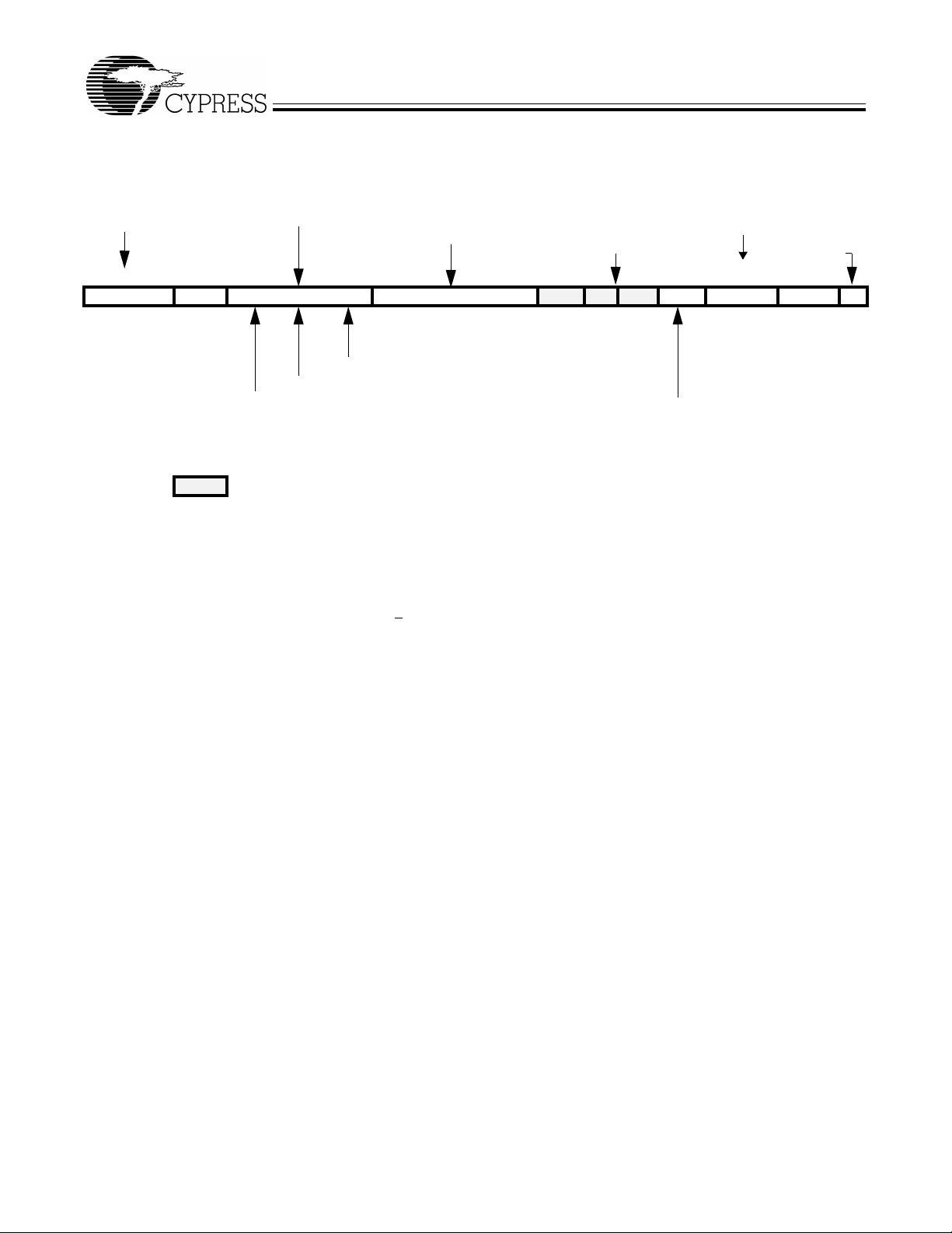
CY7C66013
CY7C66113
Table 20-2. Decode table for Table 20-3: “Details of Modes for Differing Traffic Conditions”
Properties of incoming packet
Encoding Status bits What the SIE does to Mode bits
PID Status bits Interrupt?
End Point Mode
3 2 1 0 Token count buffer dval DTOG DVAL COUNT
Setup
In
Out
The validity of the receiv ed data
The quality status of the DMA buffer
The number of received bytes Acknowledge phase completed
Setup In Out ACK 3 2 1 0 Response Int
End Point
Mode
Legend:
UC: unchanged TX: transmit TX0: transmit 0-length packet
x: don’t care RX: receive
available for Control endpoint only
The response of the SIE can be summarized as follows:
1. The SIE only responds to valid transactions and ignores non-valid ones.
2. The SIE generates an interrupt when a valid transacti on is comp leted or wh en the FIFO is co rrupted. FIF O corruption oc curs
during an OUT or SETUP transaction to a valid internal address that ends with a non-valid CRC.
3. An incoming Data packet is valid if the count is <
Endpoint Size + 2 (includes CRC) and passes all error checking.
4. An IN is ignored by an OUT configured endpoint and vice versa.
5. The IN and OUT PID status is updated at the end of a transaction.
6. The SETUP PID status is updated at the beginning of the Data packet phase.
7. The entire Endpoint 0 mode register and the count register are locked from CPU writes at the end of any transaction to that
endpoint in which either an ACK is transferred or the mode bits have changed. These registers are only unlocked by a CPU
read of these registers, and only if that read happens after the transaction completes. This represents about a 1-µs window
in which the CPU i s locke d from regis ter writes to th ese U SB regist ers. Normall y, the firmware should perform a re gister read
at the beginning o f th e End po int ISR s t o u nlo ck an d ge t th e m od e reg is ter i nformation. The interlock on the Mo de and Count
registers ensures that the firmware recognizes the changes that the SIE might have made during the previous transaction.
Document #: 38-08024 Rev. ** Page 42 of 53
Page 43

CY7C66013
CY7C66113
Table 20-3. Details of Modes for Differing Traffic Conditions (see Table 20-2 for the decode legend)
End Point Mode
3 2 1 0 token count buffer dval DTOG DVAL COUNT Setup In Out ACK 3 2 1 0 response int
PID
Setup Packet (if accepting)
See Table 20-1 Setup <= 10 data valid updates 1 updates 1 UC UC 1 0 0 0 1 ACK yes
See Table 20-1 Setup > 10 junk x updates updates updates 1 UC UC UC NoChange ignore yes
See Table 20-1 Setup x junk invalid updates 0 updates 1 UC UC UC NoChange ignore yes
Disabled
0 0 0 0 x x UC x UC UC UC UC UC UC UC NoChange ignore no
Nak In/Out
0 0 0 1 Out x UC x UC UC UC UC UC 1 UC NoChange NAK yes
0 0 0 1 In x UC x UC UC UC UC 1 UC UC NoChange NAK yes
Ignore In/Out
0 1 0 0 Out x UC x UC UC UC UC UC UC UC NoChange ignore no
0 1 0 0 In x UC x UC UC UC UC UC UC UC NoChange ignore no
Stall In/Out
0 0 1 1 Out x UC x UC UC UC UC UC 1 UC NoChange Stall yes
0 0 1 1 In x UC x UC UC UC UC 1 UC UC NoChange Stall yes
Control Write
Normal Out/premature status In
1 0 1 1 Out <= 10 data valid updates 1 updates UC UC 1 1 1 0 1 0 ACK yes
1 0 1 1 Out > 10 junk x updates updates updates UC UC 1 UC NoChange ignore yes
1 0 1 1 Out x junk invalid updates 0 updates UC UC 1 UC NoChange ignore yes
1 0 1 1 In x UC x UC UC UC UC 1 UC 1 NoChange TX 0 yes
NAK Out/premature status In
1 0 1 0 Out <= 10 UC valid UC UC UC UC UC 1 UC NoChange NAK yes
1 0 1 0 Out > 10 UC x UC UC UC UC UC UC UC NoChange ignore no
1 0 1 0 Out x UC invalid UC UC UC UC UC UC UC NoChange ignore no
1 0 1 0 In x UC x UC UC UC UC 1 UC 1 NoChange TX 0 yes
Status In/extra Out
0 1 1 0 Out <= 10 UC valid UC UC UC UC UC 1 UC 0 0 1 1 Sta ll yes
0 1 1 0 Out > 10 UC x UC UC UC UC UC UC UC NoChange ignore no
0 1 1 0 Out x UC invalid UC UC UC UC UC UC UC NoChange ignore no
0 1 1 0 In x UC x UC UC UC UC 1 UC 1 NoChange TX 0 yes
Control Read
Normal In/premature status Out
1 1 1 1 Out 2 UC valid 1 1 updates UC UC 1 1 NoChange ACK yes
1 1 1 1 Out 2 UC valid 0 1 updates UC UC 1 UC 0 0 1 1 Stall yes
1 1 1 1 Out !=2 UC valid updates 1 updates UC UC 1 UC 0 0 1 1 Stall yes
1 1 1 1 Out > 10 UC x UC UC UC UC UC UC UC NoChange ignore no
1 1 1 1 Out x UC invalid UC UC UC UC UC UC UC NoChange ignore no
1 1 1 1 In x UC x UC UC UC UC 1 UC 1 1 1 1 0 ACK (back) yes
Nak In/premature status Out
1 1 1 0 Out 2 UC valid 1 1 updates UC UC 1 1 NoChange ACK yes
1 1 1 0 Out 2 UC valid 0 1 updates UC UC 1 UC 0 0 1 1 Stall yes
1 1 1 0 Out !=2 UC valid updates 1 updates UC UC 1 UC 0 0 1 1 Stall yes
1 1 1 0 Out > 10 UC x UC UC UC UC UC UC UC NoChange ignore no
1 1 1 0 Out x UC invalid UC UC UC UC UC UC UC NoChange ignore no
1 1 1 0 In x UC x UC UC UC UC 1 UC UC NoChange NAK yes
Status Out/extra In
0 0 1 0 Out 2 UC valid 1 1 updates UC UC 1 1 NoChange ACK yes
0 0 1 0 Out 2 UC valid 0 1 updates UC UC 1 UC 0 0 1 1 Stall yes
0 0 1 0 Out !=2 UC valid updates 1 updates UC UC 1 UC 0 0 1 1 Stall yes
Set End Point Mode
Document #: 38-08024 Rev. ** Page 43 of 53
Page 44

CY7C66013
CY7C66113
Table 20-3. Details of Modes for Differing Traffic Conditions (see Table 20-2 for the decode legend) (continued)
End Point Mode
3 2 1 0 token count buffer dval DTOG DVAL COUNT Setup In Out ACK 3 2 1 0 response int
0 0 1 0 Out > 10 UC x UC UC UC UC UC UC UC NoChange ignore no
0 0 1 0 Out x UC invalid UC UC UC UC 1 UC UC NoChange ignore no
0 0 1 0 In x UC x UC UC UC UC 1 UC UC 0 0 1 1 Stall yes
PID
Out endpoint
Normal Out/erroneous In
1 0 0 1 Out <= 10 data valid updates 1 updates UC UC 1 1 1 0 0 0 ACK yes
1 0 0 1 Out > 10 junk x updates updates updates UC UC 1 UC NoChange ignore yes
1 0 0 1 Out x junk invalid updates 0 updates UC UC 1 UC NoChange ignore yes
1 0 0 1 In x UC x UC UC UC UC UC UC UC NoChange ignore no
1 0 0 1 In x UC x UC UC UC UC UC UC UC NoChange Stall no
NAK Out/erroneous In
1 0 0 0 Out <= 10 UC valid UC UC UC UC UC 1 UC NoChange NAK yes
1 0 0 0 Out > 10 UC x UC UC UC UC UC UC UC NoChange ignore no
1 0 0 0 Out x UC invalid UC UC UC UC UC UC UC NoChange ignore no
1 0 0 0 In x UC x UC UC UC UC UC UC UC NoChange ignore no
Isochronous endpoint (Out)
0 1 0 1 Out x updates updates updates updates updates UC UC 1 1 NoChange RX yes
0 1 0 1 In x UC x UC UC UC UC UC UC UC NoChange ignore no
In endpoint
Normal In/erroneous Out
1 1 0 1 Out x UC x UC UC UC UC UC UC UC NoChange ignore no
1 1 0 1 Out x UC x UC UC UC UC UC UC UC NoChange stall no
1 1 0 1 In x UC x UC UC UC UC 1 UC 1 1 1 0 0 ACK (back) yes
NAK In/erroneous Out
1 1 0 0 Out x UC x UC UC UC UC UC UC UC NoChange ignore no
1 1 0 0 In x UC x UC UC UC UC 1 UC UC NoChange NAK yes
Isochronous endpoint (In)
0 1 1 1 Out x UC x UC UC UC UC UC UC UC NoChange ignore no
0 1 1 1 In x UC x UC UC UC UC 1 UC UC NoChange TX yes
Set End Point Mode
[3]
(STALL
= 0)
[3]
(STALL
= 1)
[3]
= 0)
(STALL
[3]
(STALL
= 1)
Document #: 38-08024 Rev. ** Page 44 of 53
Page 45
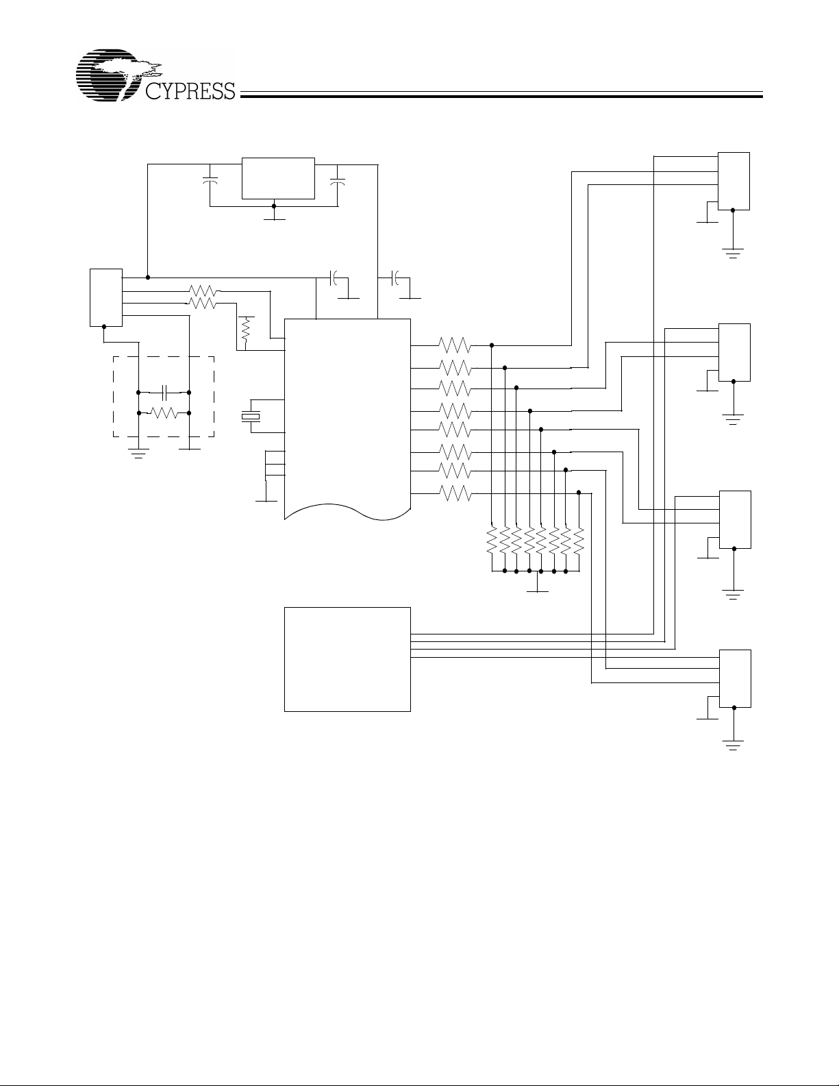
21.0 Sample Schematic
3.3V Regulator
2.2
µ
F
IN
OUT
GND
CY7C66013
CY7C66113
USB-A
Vref
2.2 µF
Vbus
D–
D+
GND
USB-B
Vbus
D–
D+
GND
SHELL
Optional
Vbus
4.7 nF
250VAC
10M
0V
22x2(R
0V
)
ext
Vref
1.5K
(R
UUP
6.000 MHz
0V
D0–
)
D0+
XTALO
XTALI
GND
GND
Vpp
0.01 µF
Vcc
0V
0.01 µF
Vref
D1–
D1+
D2–
D2+
D3–
D3+
D4–
D4+
0V
22x8(R
15K(x8)
(R
UDN
0V
USB-A
ext
)
Vbus
D–
D+
GND
0V
USB-A
Vbus
D–
D+
GND
)
0V
0V
USB-A
POWER
MANAGEMENT
Vbus
D–
D+
GND
0V
Figure 21-1. Sample Schematic
Document #: 38-08024 Rev. ** Page 45 of 53
Page 46

CY7C66013
CY7C66113
22.0 Absolute Maximum Ratings
Storage Temperature ..........................................................................................................................................–65°C to +150°C
Ambient Temperature with Power Applied.................................................................................................................0°C to +70°C
Supply Voltage on V
DC Input Voltage........................................................................................................................................... –0.5V to +V
DC Voltage Applied to Outputs in High Z State ............................................................................................ –0.5V to +V
Power Dissipation..............................................................................................................................................................500 mW
Static Discharge Voltage ...................................................................................................................................................>2000V
Latch-up Current ............................................................................................................................................................ >200 mA
Max Output Sink Current into Port 0, 1, 2, 3, and DAC[1:0] Pins ...................................................................................... 60 mA
Max Output Sink Current into DAC[7:2] Pins...................................................................................................................... 10 mA
Max Output Source Current from Port 1, 2, 3, 4 ................................................................................................................ 30 mA
23.0 Electrical Characteristics
Fosc = 6 MHz; Operating Temperature = 0 to 70°C, VCC = 4.0 to 5.25 Volts
V
V
I
CC
I
SB1
I
ref
I
il
V
V
V
C
I
lo
R
R
R
t
vccs
V
V
Z
O
R
V
V
V
V
REF
pp
di
cm
se
in
ext
UUP
UDN
UOH
UOL
up
ITH
H
OL
OH
Reference Voltage 3.15 3.45 V 3.3V ±5%
Programming Voltage (disabled) –0.4 0.4 V
VCC Operating Current 50 mA No GPIO source current
Supply Current—Suspend Mo de 50 µA
Vref Operating Current 10 mA No USB Traffic
Input Leakage Current 1 µA Any pin
Differen tial Input Sensitivity 0.2 V | (D+)–(D–) |
Differential Input Common Mode Range 0.8 2.5 V
Single Ended Receiver Threshold 0.8 2.0 V
Transceiver Capacitance 20 pF
Hi-Z State Data Line Leakage –10 10 µA0V < V
External USB Series Resistor 19 21 Ω In series with each USB pin
External Upstream USB Pull-up Resistor 1.425 1.575 kΩ 1.5 kΩ ±5%, D+ to V
External Downstream Pull-d own Resisto rs 14.25 15.75 kΩ 15 kΩ ±5%, downstream USB pins
VCC Ramp Rate 0 100 ms Linear ramp 0V to V
Static Output High 2.8 3.6 V 15 kΩ ±5% to Gnd
Static Output Low 0.3 V 1.5 kΩ ±5% to V
USB Driver Output Impedance 28 44 Ω Including R
Pull-up Resistance (typical 14 kΩ) 8.0 24.0 kΩ
Input Threshold Voltage 20% 40% V
Input Hysteresis Voltage 2% 8% V
Port 0,1,2,3 Output Low Voltage 0.4
Output High Voltage 2.4 V IOH = 1.9 mA (all ports 0,1,2,3)
relative to VSS....................................................................................................................–0.5V to +7.0V
CC
Parameter Min. Max. Unit Conditions
General
[4]
USB Interface
< 3.3V
in
REG
Power-On Reset
[5]
CC
USB Upstream/Downstream Port
REF
Resistor
ext
General Purpose I/O (GPIO)
All ports, LOW to HIGH edge
CC
All ports, HIGH to LOW edge
CC
V
IOL = 3 mA
2.0
V
I
OL
= 8 mA
CC
CC
+0.5V
+0.5V
Document #: 38-08024 Rev. ** Page 46 of 53
Page 47

Parameter Min. Max. Unit Conditions
DAC Interface
R
up
I
sink0(0)
I
sink0(F)
I
sink1(0)
I
sink1(F)
I
range
T
ratio
I
sinkDAC
I
lin
Notes:
4. Add 18 mA per driven USB cable (upstream or downstream). This is based on transitions every 2 full-speed bit times on average.
5. Power-on Reset occurs whenev er the vol ta ge on V
6. Irange: I
7. T
ratio
8.
I
measured as largest step size vs. nominal according to measured full scale and zero programmed values.
lin
DAC Pull-up Resistance (typical 14 kΩ) 8.0 24.0 kΩ
DAC[7:2] Sink Current (0) 0.1 0.3 mA V
DAC[7:2] Sink Current (F) 0.5 1.5 mA V
DAC[1:0] Sink Current (0) 1.6 4.8 mA V
DAC[1:0] Sink Current (F) 8 24 mA V
Programmed Isink Ratio: max/min 4 6 V
Tracking Ratio DAC[1:0] to DAC[7:2] 14 22 V
DAC Sink Current 1.6 4.8 mA V
Differential Nonlinearity 0.6 LSB DAC Port
is below approximately 2.5V.
CC
= I
sinkn
sink1
(15)/ I
[1:0](n)/I
(0) for the same pin.
sinkn
0[7:2](n) for the same n, programmed.
sink
= 2.0V DC
out
= 2.0V DC
out
= 2.0V DC
out
= 2.0V DC
out
= 2.0V DC
out
= 2.0V
out
= 2.0V DC
out
[6]
[7]
[8]
CY7C66013
CY7C66113
Document #: 38-08024 Rev. ** Page 47 of 53
Page 48

CY7C66013
CY7C66113
24.0 Switching Characteristics (f
= 6.0 MHz)
OSC
Parameter Description Min. Max. Unit
Clock Source
f
OSC
t
cyc
t
CH
t
CL
t
rfs
t
ffs
t
rfmfs
t
dratefs
Clock Rate 6 ±0.25% MHz
Clock Period 166.25 167.08 ns
Clock HIGH time 0.45 t
Clock LOW time 0.45 t
USB Full Speed Signaling
[9]
CYC
CYC
Transition Rise Time 4 20 ns
Transition Fall Time 4 20 ns
Rise / Fall Time Matching; (tr/tf) 90 111 %
Full Speed Date Rate 12 ±0.25% Mb/s
DAC Interface
t
sink
Current Sink Response Time 0.8 µs
HAPI Read Cycle Timing
t
RD
t
OED
t
OEZ
t
OEDR
Read Pulse Width 15 ns
OE LOW to Data Valid
OE HIGH to Data High-Z
OE LOW to Data_Ready Deasserted
[10, 11]
[11]
[10, 11]
40 ns
20 ns
0 60 ns
HAPI Write Cycle Timing
t
WR
t
DSTB
t
STBZ
t
STBLE
Write Strobe Width 15 ns
[10, 11]
[11]
[11]
5 ns
15 ns
0 50 ns
Data Valid to STB HIGH (Data Set-up Time)
STB HIGH to Data High-Z (Data Hold Time)
STB LOW to Latch_Empty Deasserted
Timer Signals
t
watch
Notes:
9. Per Table 7-6 of revision 1.1 of USB specification.
10. For 25-pF load.
11. Assumes chip select CS
Watch Dog Timer Period 8.192 14.336 ms
is asserted (LOW).
ns
ns
Document #: 38-08024 Rev. ** Page 48 of 53
Page 49
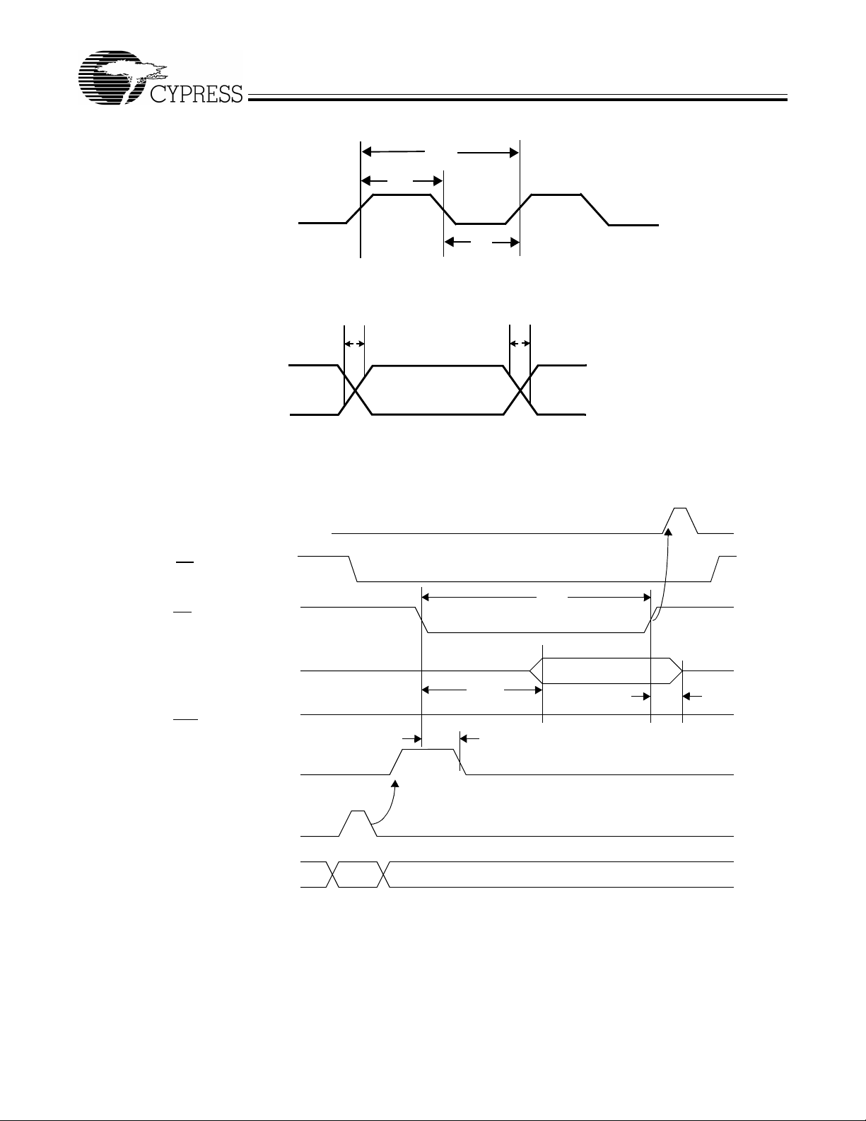
CLOCK
t
t
CH
Figure 24-1. Clock Timing
CYC
CY7C66013
CY7C66113
t
CL
D+
10%
D−
Figure 24-2. USB Data Signal Timing
Interrupt Generated
CS (P2.6, input)
OE (P2.5, in put)
DATA (output)
(P2.4, input)
STB
DReadyPin (P2.3, output)
(Shown for DRDY Polarity=0)
t
r
90%
90%
t
r
10%
Int
t
RD
D[23:0]
t
t
OEDR
OED
t
OEZ
(Ready)
Internal Write
Internal Addr
Port0
Figure 24-3. HAPI Read by External Interface from USB Microcontroller
Document #: 38-08024 Rev. ** Page 49 of 53
Page 50

CY7C66013
CY7C66113
Interrupt Generated
(P2.6, input)
CS
(P2.4, input)
STB
DATA (input)
OE (P2.5, input)
LEmptyPin (P2.2, output)
(Shown for LEMPTY Polarity=0)
Internal Read
Internal Addr
Figure 24-4. HAPI Write by External Device to USB Microcontroller
t
STBLE
t
WR
D[23:0]
t
DSTB
(not empty)
t
STBZ
Int
Port0
25.0 Ordering Information
Ordering Code PROM Size
CY7C66013-PVC 8 KB O48 48-Pin (300-Mil) SSOP Commercial
CY7C66013-PC 8 KB P25 48-Pin (600-Mil) PDIP Commercial
CY7C66113-PVC 8 KB O56 56-Pin (300-Mil) SSOP Commercial
Document #: 38-08024 Rev. ** Page 50 of 53
Package
Name Package Type
Operating
Range
Page 51
26.0 Package Diagrams
CY7C66013
CY7C66113
48-Lead Shrunk Small Outline Package O48
56-Lead Shrunk Small Outline Package O56
51-85061-*C
51-85062-*C
Document #: 38-08024 Rev. ** Page 51 of 53
Page 52

ng so indemnifies Cypress Semiconductor against all charges.
26.0 Package Diagrams (continued)
CY7C66013
CY7C66113
48-Lead (600-Mil) Molded DIP P25
51-85020-A
Document #: 38-08024 Rev. ** Page 52 of 53
© Cypress Semiconductor Corporation, 2002. The information contained herein is subject to change without notice. Cypress Semiconductor Corporation assumes no responsibility for the use
of any circuitry other than circuitry embodied in a Cypress Semiconductor product. No r does it convey or imply any license under patent or other rights. Cypress Semiconductor does not autho rize
its products for use as critical components in life-support systems where a malfunction or failure may reasonably be expected to result in significant injury to the user. The inclusion of Cypress
Semiconductor products in life-support systems application implies that the manufacturer assume s all risk of such use and in doi
Page 53

CY7C66013
CY7C66113
Document Title: CY7C66013, CY7C66113 Full-Speed USB (12 Mbps) Peripheral Controller with Integrated Hub
Document Number: 38-08024
REV. ECN NO.
** 114525 3/27/02 DSG Change from Spec number: 38-00591 to 38-08024
Issue
Date
Orig. of
Change Description of Change
Document #: 38-08024 Rev. ** Page 53 of 53
 Loading...