

Page 1

PRELIMINARY
™
ily
x
CY7C656x
EZ-USB HX2LP
Low-Power USB 2.0 Hub Controller Fam
1.0 Features
• USB 2.0 hub controller
• Compliant with the USB 2.0 specification
• Windows
• Up to four downstream ports supported
• Supports bus-power and self powered modes
• Single-TT and Multi-TT modes supported
—Single-TT option for low-cost
—Multi-TT option for high performance
•2-Port
—Single TT option for bus power
• Fit/form/function compatible option with CY7C65640
(TetraHub)
• Multiple package options
—Space -saving 56 QFN
• Single power supply requirement
—Internal regulat or for reduced cost
• Integrated up stream pull-up resist or
• Integrated pull -down resistors for a ll downstream port s
• Integrated up stream and downstream terminati on
resistors
• Integrated port status indicator controls
• 24-MHz external crystal (inte grated PLL)
• Configurable with external SPI EEPROM
—Ven dor ID, Product ID, Device ID (VID/PID/DID)
—N um ber of active ports
—N um ber of removable ports
—Maximum power setting for high-speed and full-
speed
—H ub controller power setting
—Power-on timer
—Overcurrent detection mode
—Overcurrent timer
—Enable/Disable overcurrent timer
—Overcurrent pin polarity
—indicator pin polar ity
—Compound device
—Enable full-speed only
—Disable port indicators
—Gang power switching
—Enable single-TT mode only
—Self/bus powered compatibility
—Fully configurable string descriptors for multiple
language support
• In-system EEPROM programming
Hardware-quality lab (WHQL)-compliant
2.0 Introduction
EZ-USB HX2LP is Cypress’s nex t- generat ion fami ly of highperformance, low-powe r USB 2.0 hub controllers. HX2LP is an
ultra low-power single-chip USB 2.0 hub controller with
integrated upstream and downstream transceivers, a USB
Serial Inter face Engine (SIE), USB Hub Con tr ol and Repeate r
logic, and T ransac tion T ranslat or (TT) l ogic. Cypress has also
integrated many of the external passive component s, such as
pull-up and pull-down resistors, reducing the overall bill-ofmaterials required to implement a hub design. The entire
HX2LP portfolio consi sts of:
1. CY7C65640B (TetraHub LP): 4-port/multiple transaction
translator
This device option is fit/form/function compatible with Cypress’s existing CY7C65640 device. Cypress’s “Tetra” architecture provi des four downstream USB ports, each with
a dedicated T ransact ion T ranslator (TT), maki ng it t he highest-performance hub available. The TetraHub LP also offers best-in-class power consumption. The CY7C65640B is
available in a 56 QF N (TetraHub pin-compatible) for space
saving designs.
2. CY7C65630: 4-port/single transaction translator
This device option is for ultra low-cost applications where
performance is secondary consideration. All four ports
must share a single transaction translator in this configuration. The CY7C65630 is available in a 56 QFN and is also
pin for pin-compatible with the CY7C65640.
3. CY7C65620:
This device option is for a 2-port bus powered application.
Both ports must share a single transaction translator in this
configuration. The CY7C65620 is available in a 56 QFN
and is also pin for pin compatible with the CY7C65640.
All device options are supported by Cypress’s world-class
reference design kits, which include board schematics, bill of
materials, Gerber files, Orcad files, and thorough design
documentation.
Cypress Semiconductor Corporation • 3901 North First Street • San Jose, CA 95134 • 408-943-2600
Document #: 38-08037 Rev. *D Revised March 31, 2005
Page 2
x
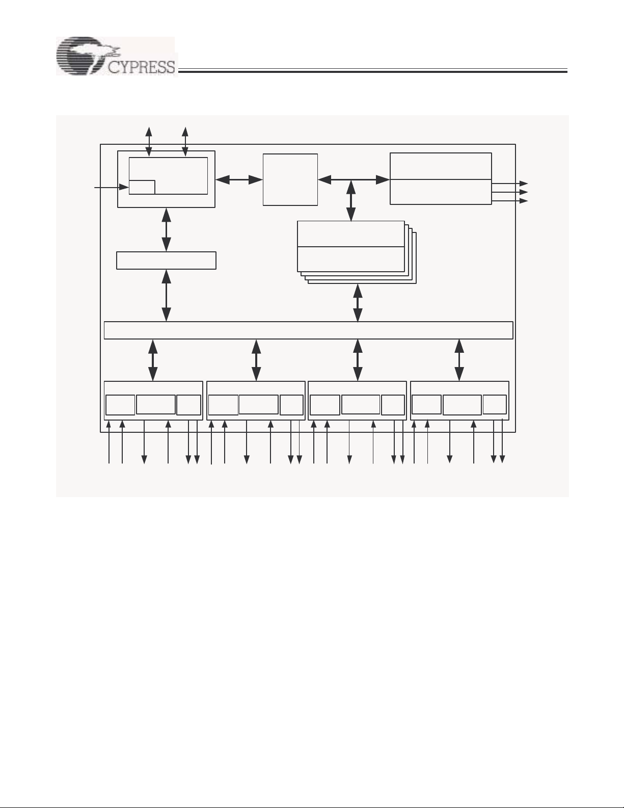
3.0 Block Diagrams
D+ D -
PRELIMINARY
CY7C656x
24
MHz
Crystal
USB 2.0 PHY
PLL
USB Upstream Port
Hub Repeater
USB Downstream Port 1
USB 2.0
PHY
Port Power
Control
Port
Status
Interface
USB Downstream Port 2
USB 2.0
PHY
Port Power
Control
Serial
Engine
Transaction Translator (X4)
Routin g L o gi c
USB Downstream Port 3
Port
Status
USB 2.0
PHY
TT RAM
Port Power
Control
USB Control Logic
SPI Communication
Port
Status
USB 2.0
High-Speed
Block
USB Downstream Port 4
PHY
Port Power
Control
Port
Status
SPI_SCK
SPI_SD
SPI_CS
OVR #[ 1 ]
LED
OVR #[ 2 ]
LEDD+ D- P WR#[1]
OVR#[3]
LEDD+ D- PWR#[2]
D+ D- PWR#[4]
OVR #[ 4 ]
LEDD+ D- PWR#[3]
Figure 3-1. CY7C65640B Block Diagram
Document #: 38-08037 Rev. *D Page 2 of 23
Page 3
x
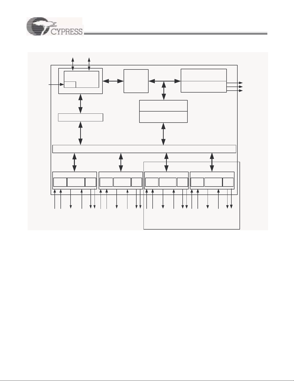
3.0 Block Diagrams (continued)
D+ D -
PRELIMINARY
CY7C656x
24 MHz
Crys ta l
USB 2.0 PHY
PLL
USB Upstream Port
Hub Repeater
USB Downstream Port 1
USB 2.0
Port Power
PHY
Control
OVR # [1]
Port
Status
LED
Interface
USB Downstream Port 2
USB 2.0
Port Power
PHY
Control
OVR # [2]
Serial
Engine
Transac t ion Translator (X1)
Routing Logic
USB Downstream Port 3
Port
USB 2.0
Status
PHY
LEDD+ D- P W R#[1]
TT RA M
Port Power
Control
OVR # [3]
USB C ontrol Logi c
SPI Communication
Port
USB 2 .0
Status
D+ D- PW R#[ 4 ]
LEDD+ D- PWR#[2]
High-Speed
Block
USB Downstream Port 4
PHY
Port Power
Control
OVR#[4]
Port
Status
SPI_SCK
SPI_SD
SPI_CS
LEDD+ D- PW R#[3]
This applies to CY7C65630 only.
Figure 3-2. CY7C65630/CY7C65620 Block Diagram
Document #: 38-08037 Rev. *D Page 3 of 23
Page 4

x
PRELIMINARY
CY7C656x
3.1 USB Serial Interface Engine (SIE)
The SIE allows the CY7C656x x to commu nicate wit h the USB
host through the USB repeater component of the HUB. The
SIE handles the following USB activity independently of the
HUB Control Block:
• Bit stuffing/unstuffing
• Checksum generation/checking
• ACK/NAK/STALL
• TOKEN type identification
• Address checking.
3.2 Hub Repeater
The HUB Repeater manages the connectivity between
upstream and downstream facing ports that are operating at
the same speed. It supports full-/low-speed connectivity and
high-speed connectivity. Per the USB 2.0 specification, the
HUB Repeater provides the following functions:
• Sets up a nd tears down connectivity on packet boun daries
• Ensures orderly entry into and out of the Suspend state,
including proper handling of remote wakeups.
3.3 Transaction T r anslator (TT)
The TT basically transl ates dat a from one sp eed to another. A
TT takes high-speed split transactions and translates them to
full-/low-speed transactions when the HUB is operating at
high-speed (the upstream port is connected to a high-speed
host controller) and has full-/low-speed devices at tached. The
operating spee d of a device at tached on a downstream fac ing
port determi nes whether the Routing Logi c connects a port to
the Transaction Translator or Hub Repeater section. If a low/full-speed device is connected to the hub operating at highspeed, the data transfer route includes the transaction translator. If a high-speed device is connected to this high-speed
hub the route only includes the repeater and no transaction
translator since the device and the hub are in conformation
with respect to their data transfer speed. When the hub is
operating at full speed (the upstream port is connected to a
full-speed host controller), a high-speed peripheral will not
operate at its f ull capabi lity . The se devices will onl y work at 1.1
speed. Full- and low-speed devices connected to this hub will
operate at their 1. 1 speed.
4.0 Applications
• Ty pical applications for the HX2LP device family are :
• St andalone hubs
• Motherboard hubs
• Monitor hubs
• Advanced port replicators
• Docking stations
• Split-PC designs
• External personal storage drives
• Keyboard hubs
5.0 Functional Overview
The Cypress CY7C656xx USB 2.0 Hubs are a high-performance, low-system-cost solution for USB. The CY7C656xx
USB 2.0 Hubs integrate 1.5k up stream pull-up resi stors for fullspeed operation and all downstream 15k pull-down resistors
as well as series termination resistors on all upstream and
downstream D+ and D– pins. This results in optimization of
system costs by providing built-in support for the USB 2.0
specification.
5.1 System Initialization
On power-up, the CY7C656xx will read an external SPI
EEPROM for configuration information. At the most basic
level, this EEPROM will have the Vendor ID ( VID) , Product ID
(PID), and Device ID (DID) for the customer 's application. For
more speciali zed appl icati ons, othe r conf igurat ion opt ions can
be specified. See secti on 9.0 for more detail s.
After reading the EEPROM, if BUSPOWER (connected t o upstream VBus) is HIGH, CY7C656xx will enable the pull-up
resistor on the D+ to indicate that it is connected to the
upstream hub, after which a USB Bus Reset is expected.
During this reset, CY7C656xx will initiate a chirp to indicate
that it is a high-speed peripheral. In a USB 2.0 system, the
upstream hub will respond with a chirp sequence, and
CY7C656xx will be in a high-speed mode, with the upstream
D+ pull-up resistor turned off. In USB 1.x systems, no such
chirp sequence from the upstream hub will be seen, and
CY7C656xx will op erat e as a normal 1. x hub (operating at full
speed).
5.2 Enume ration
After a USB Bus Reset, CY7C656xx is in an unaddressed,
unconfigured state (configuration value set to 0). During the
enumeration process, the host will set the hub's address and
configuration by sending a SetCongfiguration request.
For high-speed multi-TT support, the host must also set the
alternate inter face set ting t o 1 (the defau lt mode is singl e-TT) .
Once the hub is configured, the full hub functionality is
available.
5.3 Multiple Transaction Translator Support
After the CY7C65640B is configured in a high-speed system,
it will be in Singl e TT mode. The host may t hen set the hub into
Multiple TT mode by sending a SetInterface command. In
Multiple TT mode, each full speed port is handled independently and thus has a full 12-Mbps bandwidth available. In
Single TT mode, all traffic from the host destined for full- or
low-speed ports will be forwarded to all of those ports. This
means that the 12-Mbps bandwidth is shared by all full- and
low-speed ports.
5.4 Down stream P orts
The CY7C656xx supports a maximum of four downstream
ports, each of which may be marked as usable or removable
in the extended configuration (0xD2 EEPROM load, see
section 9.2 or 0xD4 EEPROM load, see section 9.3).
Downstream D+ and D– pull-down resistors are incorporated
in CY7C656xx for each port. Prior to the hubs being
configured, the ports are driven SE0 (Single Ended Zero,
where both D+ and D– are driven low) and are set to the
Document #: 38-08037 Rev. *D Page 4 of 23
Page 5

x
PRELIMINARY
CY7C656x
unpowered stat e. Once the hubs ar e configu red, the por ts ar e
not driven, and the host may power the ports by sending a
SetPortPower command to each port. After a port is powered,
any connect or disconnect event is detected by the hub. Any
change in the port state is reported by the hubs back to the
host through the Status Change Endpoint (endpoint 1). Upon
receipt of SetPort R eset command from the host, the hub will
• Drive SE0 on the corresponding port
• Put the port in an enabled state
• Enable the green por t indicator for that port (i f not previously
overridden by t he host)
• Enable babble detection once the port is enabl ed.
Babble consists of either unterminated traffic from a
downstream port (o r loss of activi ty), or a non-idle condi tion on
the port after EOF2. If babble is detected on an enabled port,
that port will be disabl ed. A Cle arPort Enable comm and from
the host will also disable the specifie d port.
Downstream ports can be individually suspended by the host
with the SetPortSuspend command. If the hubs are not
suspended, any res ume will be con fined t o that in divid ual port
and reflected to the host through a port change indication in
the Hub Status Change Endpoint. If the hubs are suspended,
a resume on this port will be forwarded to the host, but other
resume events will not be seen on that port. The host may
resume the port by sendi ng a ClearPortSuspend com m and.
5.5 Upstream Port
The upstream port includes the transmitter and the receiver
state machine. The Transmitter and Receiver operate in highspeed and full-speed depending on the current hub configuration.
The transmitter state machine monitors the upstream facing
port while the Hub Repeater has conn ectivity in the upstr eam
direction. This monitoring activity prevents propagation of
erroneous indications in the upstream direction. In particular,
this machine prevents babble and disconnect events on the
downstream facing ports of this hub from propagating and
causing the hub to be disabled or disconnected by the hub to
which it is att ached. This all ows the Hub to only disco nnect th e
offensi ve port on detecting a babble from it.
5.6 Power Switching
The CY7C656xx includes interface signals for external port
power switches. Both ganged and individu al (per-por t) confi gurations are supported, with individual switching being the
default. Initially all ports are unpowered. After enumerating,
the host may power each port by sending a SetPortPower
command for that port. The power switching and over-current
detection of downstream ports is managed by control pins
connected to an external power switch device. PWR [n]#
output pins of the CY7C656xx series are connected to the
respective external power switch's port power enable signals.
(Note that each port power output pin of the external power
switch must be bypassed with an electrolytic or tantalum
capacitor as required by the USB specification. These capacitors supply the inrush currents, which occur during
downstream device hot-attach events.) The polarity of t his pin
can be configured through the EEPROM, see section 9.3.
5.7 Over-current Detection
Over-current detection includes timed detection of 8 ms by
default. This parameter is configured from the external
EEPROM in a range of 0 ms to 15 m s for both an enabled por t
and a disabled port individually. Detection of over-current on
downstream ports is managed by control pins conn ected to an
external power switch device.
The OVR[n]# pins of the CY7C656xx serie s are connected to
the respective external power switch's port over-current
indication (output) signals. Upon detecting an over-current
condition, the hub device r eports the over-current condition to
the host and disables the PWR# output to the external power
device. The polarity of this pin can be configured through the
EEPROM, see section 9.3.
5.8 Port I ndicators
The USB 2.0 port indicators are also supported directly by the
CY7C656xx. As per the specification, each downstream port
of the hub support s an opti onal st atus i ndicat or. The presence
of indicators for downstream facing ports is specified by bit 7
of the wHubCharacteristics field of the hub class descriptor.
The default CY7C656xx descriptor specifies that port
indicators are supported (wHubCharacteristics, bit 7 is set). If
port indicators are not included in the hub, this should be
disabled by the EEPROM.
Each port indicator is strategically located directly on the
opposite edge of the port which it is associated with. The
indicator provides two colors: green an d am ber. This is implemented as two separate LEDs, one amber and the other
green. A combi nation of hardware and soft ware contr ol is u sed
to inform t he user of the cur rent stat us of the port or the d evice
attached to the port and to guide the user through problem
resolution. Colors and bl inking are use d to provide infor mation
to the user . The signific ance of the color of th e LED depend on
the operational mode of the CY7C656xx. There are tw o modes
of operation for the CY7C656xx port indicat ors: automatic and
manual.
On power-up the CY7C656xx defaults to Automatic Mode,
where the color of the Port Indicator (Green, Amber, Off)
indicates the functional status of the CY7C656xx port. In
Automatic Mode, the CY7C656xx will turn on the green LED
whenever the port is en abled and the amber LED when i t has
had an overcurrent condition detected. The color of the port
indicator is se t by the p ort st ate m achine . Bli nking of the LEDs
is not supported in Automat ic Mode. Table 5-1 below identifies
the mapping of color to port state in Automatic Mode.
T able 5-1. Automatic Port State to Port Indicator Color Mapping
Downstream Facing Hub Port State
Powered Off
Off or Amber if due to an
Overcurrent Condition
Document #: 38-08037 Rev. *D Page 5 of 23
Disconnected, Disabled, Not
Configured, Resetting, Testing
Off Green Off
Enable d , Transmit, or
TransmitR
Suspended, Resuming,
SendEOR, Restart _E /S
Page 6

x
PRELIMINARY
CY7C656x
The LED control lines can also be modulated with a square
wave for power conservat ion in s ystems u sing batteri es. Alon e
with this there is also a polarity control for these pins, see
section 9.3.
In manual mode, the indicators are under the control of the
host, which can turn on one of the LEDs, or leave them off.
This is done by a system software USB Hub class request.
Blinking of the LEDs is supported in Manual Mode. The port
indicators allow the user to intervene on any error detection.
For example, when babble is detected on plugging in a
defective device, o r on occur rence of a n overcu rrent con dition,
the port indicators corresponding to the downstream port will
blink green or only light the amber LED, respecti vely.
Note:
1. Information presented in Table 5-1 and Table 5-2 is from USB 2.0 specification Tables 11-6 and 11-7, respectively.
Table 5-2 displays the color definition of the indicators when
CY7C656xx is in Manual Mode.
T able 5-2. Por t Indica tor Color Definitions i n Manual Mode
Color Definition Port Stat e
Off Not operational
Amber Error condition
Green Fully Operational
Blinking Off/Green Software At tention
Blinking Off/ Am ber Hardware Attention
Blinking Green/Amber Reserved
[1]
Document #: 38-08037 Rev. *D Page 6 of 23
Page 7

x
6.0 Pin Configuration
PRELIMINARY
CY7C656x
DD–[4]/NC
DD+[4]/NC
VCC
GND
DD–[3]/NC
DD+[3]/NC
VCC
GND
DD–[2]
DD+[2]
VCC
GND
PWR#[3]/NC
VCC
545556
OVR#[3]/NC
53 52
PWR#[4]/NC
GND
OVR#[4]/NC
51 50 49 48 47 46 45 44 43
SPI_SD
GND
SPI_SCK
RESET
1
2
3
4
5
6
7
8
9
10
11
SELFPWR
AMBER#[4]/NC
GREEN#[4]/NC
AMBER#[3]/NC
42
41
GREEN#[3]/NC
GND
40
VCC
39
38
AMBER#[2]
GREEN#[2]
37
AMBER#[1]
36
GREEN#[1]
35
GND
34
33
VCC
OVR#[2]
32
GND
12
DD–[1]
13
DD+[1]
14
VCC
Note:
2. NC are for CY7C65620 ONLY.
D–
D+
GND
VCC
XIN
GND
VCC
XOUT
GND
SPI_CS
VBUSPOWER
Figure 6-1. 56-pin Quad Flat Pack No Leads (8 mm x 8 mm)
PWR#[2]
31
OVR#[1]
30
PWR#[1]
29
2827262524232221201918171615
VCC
GND
[2]
Document #: 38-08037 Rev. *D Page 7 of 23
Page 8

x
7.0 Pin Description Table
Table 7- 1 below displays the pin assignments.
T able 7-1. Pin Assignments
CY7C65640B /
CY7C65630 Pin
CY7C65620
Pin Name Type Default Description
3 3 VCC Power N/A V
7 7 VCC Power N/A V
11 11 VCC Power N/A V
15 15 VCC Power N/A V
19 19 VCC Power N/A V
23 23 VCC Power N/A V
27 27 VCC Power N/A V
33 33 VCC Power N/A V
39 39 VCC Power N/A V
55 55 VCC Power N/A V
4 4 GND Power N/A GND. Connect to Ground with as short a path as possible.
8 8 GND Power N/A GND. Connect to Ground with as short a path as possible.
12 12 GND Power N/A GND. Connect to Ground with as short a path as possible.
16 16 GND Power N/A GND. Connect to Ground with as short a path as possible.
20 20 GND Power N/A GND. Connect to Ground with as short a path as possible.
24 24 GND Power N/A GND. Connect to Ground with as short a path as possible.
28 28 GND Power N/A GND. Connect to Ground with as short a path as possible.
34 34 GND Power N/A GND. Connect to Ground with as short a path as possible.
40 40 GND Power N/A GND. Connect to Ground with as short a path as possible.
47 47 GND Power N/A GND. Connect to Ground with as short a path as possible.
50 50 GND Power N/A GND. Connect to Ground with as short a path as possible.
56 56 GND Power N/A GND. Connect to Ground with as short a path as possible.
21 21 XIN Input N/A 24-MHz Crystal IN or External Clock Input.
22 22 XOUT OutputN/A 24-MHz Crystal OUT.
[3]
PRELIMINARY
. This signal provid es power to the chip.
CC
. This signal provid es power to the chip.
CC
. This signal provid es power to the chip.
CC
. This signal provid es power to the chip.
CC
. This signal provid es power to the chip.
CC
. This signal provid es power to the chip.
CC
. This signal provid es power to the chip.
CC
. This signal provid es power to the chip.
CC
. This signal provid es power to the chip.
CC
. This signal provid es power to the chip.
CC
CY7C656x
46 46 RESET# I nput N/A Active LOW Reset. This pin resets the entire chip. It is
normally tied to V
through a 0.1-µF capac itor . Other than this, no other special
through a 100K resistor, and to GND
CC
power-up procedur e is required.
45 45 SELFPWR Input N/A Indicator for bus/se lf powered. 0 is bus powered, 1 is self-
powered.
26 26 VBUSPOWER Input N/A VBUS. Connect to the VBUS pin of the upstream connector.
This signal indicates to the hub that it is in a connected st ate,
and may enable the D+ pull-up resistor to indicate a
connection. (The hub will do so afte r the ext ernal EEPROM is
read, unless it is put into a high-speed mode by the upstr eam
hub).
SPI Interface
25 25 SPI_CS O O SPI Chip Select. Connect to CS pin of the EEPROM.
48 48 SPI_SCK O O SPI Clock. Connect to EEPROM SCK pin.
49 49 SPI_SD I /O/Z Z SPI Dataline Connect to GND wi th 15- KΩ
resistor and to t he
Data I/O pins of the EEPROM.
Note:
3. Unused port DD+/DD– lines can be left floating. The port power, amber, and green LED pins should be left unconnected, and the overcurrent pin should be
tied HIGH. The overcurrent pin is an input and it should not be left floating.
Document #: 38-08037 Rev. *D Page 8 of 23
Page 9

x
PRELIMINARY
CY7C656x
T able 7-1. Pin Assignments (continued)
CY7C65640B /
CY7C65630 Pin
Upstream Port
17 17 D– I/O/Z Z Upstream D– Signal.
18 18 D+ I/O/Z Z Upstream D+ Signal.
Downstream Port 1
13 13 DD–[1] I/O/Z Z Downstream D– Signal.
14 14 DD+[1] I/O/Z Z Downstream D+ Signal.
36 36 AMBER#[1] O 1 LED. Driver output for Ambe r LED. Port I ndicator Support.
35 35 GREEN#[1] O 1 LED. Driver output for Green LED. Port Indicator Support.
30 30 OVR#[1] Input 1 Overcurrent Condition Detection Input. Defau lt is Active
29 29 PWR#[1] O/Z Z Power Switch Driver Output. Default is Ac tive LOW . Po lari ty
Downstream Port 2
9 9 DD–[2] I/O/Z Z Downstream D– Signal.
10 10 DD+[2] I/O/Z Z Downstream D+ Signal.
38 38 AMBER#[2] O 1 LED. Driver output for Ambe r LED. Port I ndicator Support.
37 37 GREEN#[2] O 1 LED. Driver output for Green LED. Port Indicator Support.
32 32 OVR#[2] Input 1 Overcurrent Condition Detection Input. Defau lt is Active
31 31 PWR#[2] O/Z Z Power Switch Driver Output. Default is Ac tive LOW . Po lari ty
Downstream Port 3
5 - DD–[3] I/O/Z Z Downstream D– Signal.
6 - DD+[3] I/O/Z Z Downstream D+ Signal.
42 - AMBER#[3] O 1 LED. Driver output for Amber LED. Port Indicator Support.
41 - GREEN#[3] O 1 LED. Driver output for Green LED. Port Indicator Support.
53 - OVR#[3] Input 1 Overcurrent Condition Detection Input. Defa u lt is Active
54 - PWR#[3] O/Z Z Power Switch Driver Output. Default is Acti ve LOW . Pola rity
Downstream Port 4
1 - DD–[3] I/O/Z Z Downstream D– Signal.
2 - DD+[3] I/O/Z Z Downstream D+ Signal.
44 - AMBER#[3] O 1 LED. Driver output for Amber LED. Port Indicator Support.
43 - GREEN#[3] O 1 LED. Driver output for Green LED. Port Indicator Support.
51 - OVR#[3] Input 1 Overcurrent Condition Detection Input. Defa u lt is Active
52 - PWR#[3] O/Z Z Power Switch Driver Output. Default is Acti ve LOW . Pola rity
CY7C65620
Pin Name Type Default Description
[3]
Default is Active LOW . Polarity is control led through EEPROM.
Default is Active LOW . Polarity is control led through EEPROM.
LOW. Polarity is controlled through EEPROM.
is controlled th rough EEPROM.
Default is Active LOW . Polarity is control led through EEPROM.
Default is Active LOW . Polarity is control led through EEPROM.
LOW. Polarity is controlled through EEPROM.
is controlled th rough EEPROM.
Default is Active LOW . Polarity is control led through EEPROM.
Default is Active L OW. Polarity is controlled thro ugh EEPROM.
LOW. Polarity is controlled through EEPROM.
is controlled th rough EEPROM.
Default is Active L OW. Polarity is controlled thro ugh EEPROM.
Default is Active L OW. Polarity is controlled thro ugh EEPROM.
LOW. Polarity is controlled through EEPROM.
is controlled th rough EEPROM.
Document #: 38-08037 Rev. *D Page 9 of 23
Page 10

x
PRELIMINARY
CY7C656x
8.0 Default Descriptors
8.1 Device Descriptor
The standard devi ce descript or for CY7C656x x is based on the VID, PID, and DID found in the SPI EEPROM. This VID/PID/DID
in the EEPROM will overwr ite the def au l t V ID/PID/D ID . If no EEPROM is used, the CY7C656xx will enumer ate w ith t h e d e fa u lt
descriptor values as shown below.
Byte Full Speed High Speed Field Name Description
0 0x12 0x12 bLength 18 Bytes
1 0x01 0x01 bDescriptorType DEVICE_DESCRIPTOR
2,3 0x0110 0x 0200 bcdUSB USB specif ic ati on 2.0 in HS (1.1 if forced FS)
4 0x09 0x09 bDeviceClass HUB
5 0x00 0x00 bDeviceSubClass None
6 0x00 0x01
[4]
7 0x40 0x40 bMaxPacketSize0 64 bytes
8,9 0x04B4 0xx04B4 wIdV endor VID (overwritten by what is defined in EEPROM)
10,11 0x6560 0x6560 wIdProduct PID (overwritten by what is defined in EEPROM)
12, 13 0x0910
0x0810
0x0910
0x0810
14 0x00 0x00 iManufacturer No ma nufacturer stri ng supported
15 0x00 0x00 iProduct No product string supported
16 0x00 0x00 iSerialNumber No serial string supported
17 0x01 0x01 bNumConfigurations One configuration supported
8.2 Configuration Descriptor
Byte Full Speed High Speed Field Name Description
0 0x09 0x09 bLength 9 Bytes
10x02
[7]
2 0x0019
0x0029
/ 0x07
[8]
0x02
[7]
0x0019
0x0029
4 0x01 0x01 bNumInterfaces 1
5 0x01 0x01 bConfigurationValue The configuration to be used
6 0x00 0x00 iConfiguration
70xA0
0xE0
0xA0
0xE0
80x280x57
8.3 Interface Descriptor
Byte Full Speed High Speed Field Name Description
0 0x09 0x09 bLength 9 Bytes
1 0x04 0x04 bDescriptorType I NTERFACE_DESCRIPTOR
2 0x00 0x00 bInterfaceNumber
3 0x00 0x00 bAlternateSetting
4 0x01 0x01 bNumEndpoints
5 0x09 0x09 bInterfaceClass
6 0x00 0x00 bInterfaceSubClass
70x00
[4]
8 0x00 0x00 iInterface
Notes:
4. If configured as single-TT hub.
5. If configured as multi-TT hub and other speed.
6. This value is configured through the External EEPROM.
7. Configured speed descriptor
8. Other speed descriptor
/ 0x01
[5]
0x00
[4]
/ 0x02
/ 0x07
[4]
[5]
[6]
/ 0x01
[5]
bDeviceProtocol None
wbcdDevice DID (overwritten by what is defined in EEPROM)
[8]
bDescriptorType CONFIG_DESCRIPTOR
wTotalLength Length of all other descriptors
bmAttributes Value depends on pin 45 - SELFPWR signal
SELFPWR = 0 yields 0xA0 and =1 yields 0xE0
bMaxPower
[5]
bInterfaceProtocol
Document #: 38-08037 Rev. *D Page 10 of 23
Page 11

x
PRELIMINARY
8.4 Endpoint Descriptor
Byte Full Speed High Speed Field Name Description
0 0x07 0x07 bLength 7 Bytes
1 0x05 0x05 bDescriptorTy pe ENDPOI NT_DESCRIPTOR
2 0x81 0x81 bEndpointAddress IN Endpoint #1
3 0x03 0x03 bmAttributes Interrupt
4,5 0x0001 0x0001 wMaxPacketSize Maximum Packet Size
6 0xFF 0x0C bIn te r va l Pollin g Ra te
CY7C656x
8.5 Interface Descriptor
Byte Full Speed High Speed Field Name Description
0 N/A 0x09 bLength 9 Bytes
1 N/A 0x04 bDescriptorType INTERFACE_DESCRIPTOR
2 N/A 0x00 bInterfaceNumber Interface Descriptor Index
3 N/A 0x01 bAlternateSetting Al ternate Setting for the Interface
4 N/A 0x01 bNumEndpoints Number of Endpoints Defined
5 N/A 0x09 bInterfaceClass Interface Class
6 N/A 0x00 bInterfaceSubClass Interf ace Sub-Class
7 N/A 0x02 bInterfaceProtocol Interface Protocol
8 N/A 0x00 bInterface Interface String Index
8.6 Endpoint Descriptor
Byte Full Speed High Speed Field Name Description
0 N/A 0x07 bLength 7 Bytes
1 N/A 0x05 bDescriptorType ENDPOINT_DESCRIPTOR
2 N/A 0x81 bEndpointAddress IN Endpoint #1
3 N/A 0x03 bmAttributes Interrupt
4,5 N/A 0x0001 wMaxPacketSize Maxi mu m Pack et Si ze
6 N/A 0x0C bInterval Polling Rate
[9,10]
[9,10]
8.7 Device Qualifier Descriptor
Byte Full Speed High Speed Field Name Description
0 0x0A 0x0A bLength 10 Bytes
1 0x06 0x06 bDescriptorType DEVICE_QUALIFIER
2,3 0x0200 0x0200 bcdUSB
4 0x09 0x09 bDeviceClass
5 0x00 0x00 bDeviceSubClass
60x01
7 0x40 0x40 bMaxPacketSize0
8 0x01 0x01 bNumConfigurations
9 0x00 0x00 bReserved
Note:
9. If CY7C65640B is configured for singled-TT only or CY7C65630 or CY7C65620 (from the external EEPROM), this descriptor is not present.
10. If connected at high-speed
Document #: 38-08037 Rev. *D Page 1 1 of 23
0x02
[4]
[5]
0x00 bDeviceProtocol
Page 12

x
PRELIMINARY
8.8 Hub Descriptor
Byte All Speed Field Name Description
0 0x09 bLength 9 Bytes
1 0x29 b D escriptorType HUB Descriptor
0x02
0xAE
[11]
bNbrPorts Number of ports supported, CY7C65640B or CY7C65630.
Number of ports supported, CY7C65620.
[11]
wHubCharacteristics b1, b0: Logical Power Swi tching Mode
00: Ganged power switc hing (all ports’ power at once)
01: Individual port power switching (Def ault in CY7C656xx)
b2: Identifies a Compound Device,
0: Hub is not part of a compound device (Default in CY7C656xx),
1: Hub is part of a compound device.
b4, b3: Over-current Protection Mode
00: Global Overcurrent Protection. The hub reports over current as a
summation of all ports current draw, without a breakdown of individual
port overcurrent status.
01: Individual Port Overcurrent Protection. The hub reports overcurrent on
a per-port basis. Each port has an ov er- curre nt st atus ( Default in CY7C656 xx) .
1X: No Overcurrent Prot ection. This option is al lowed only for bus-powere d
hubs that do not implem ent overcurrent prot ection.
b6, b5: TT Think Time
00: TT requires at most 8 FS bit ti me s of i nter transaction gap on a
full-/low-speed downstream bus (Default in CY7C656xx).
b7: Port Indicators Supported,
0: Port Indicators are not supported on i ts downstream facing ports and
the PORT_INDICATOR request has no effect.
1: Port Indicators are supported on its downstream facing port s and the
PORT_INDICATOR request controls the indicators. See Section 5.0 and 10.0
(Default in CY7C656xx).
b15,. b8: Reserved
[11]
bPwrOn2PwrGood Time from when the port is powered to when the power is good on that port
[11]
bHubContrCurrent Maximum current requirement for the Hub Controll er at full-speed.
[11]
[11]
bDeviceRemov able Indicates if the port has a removabl e device attached
[11]
bPortPwrCtrlMask Required for compatibility with software written f or 1. 0 com pliant devices
Maximum current requirement for the Hub Controller at high-speed.
20x04
3,4 0x0089
50x32
60x28
70x00
80xFF
Note:
11. This value is configured through the External EEPROM.
CY7C656x
9.0 Configuration Options
Systems using CY7C656xx that do not have the fuse ROM
pre-set at the fact ory mus t have an ext ernal EEPROM in or der
for the device to have a unique VID, PID, and DID. The
CY7C656xx can communicate with SPI EEPROM that are
either double byte addressed or a single byte with the 9th bit
within the inst ruction byte, such as the 24LC040 parts use. The
25LC080 EEPROM uses t he double byte addr ess format , and
therefore the CY7C656xx can communicate with these parts.
The '010s and '020s uses the s am e command for m at as used
to interface wi th the ‘ 040 and hen ce th ese ca n also be us ed to
interface with the CY7C656xx.
Document #: 38-08037 Rev. *D Page 12 of 23
9.1 Default – 0xD0 Load
When used in default mode, only a unique VID, PID, and DID
must be present in the external SPI EEPROM. The contents
of the EEPROM must contain this information in the following
format:
Byte Value
00xD0
1 VID (LSB)
2 VID (MSB)
3 PID (LSB)
4 PID (MSB)
5 reversed
6 DID (MSB)
Page 13

x
PRELIMINARY
CY7C656x
9.2 Configured – 0xD2 Load
Byte Value (MSB->LSB)
00xD2
1 VID (LSB)
2 VID (MSB)
3 PID (LSB)
4 PID (MSB)
5reversed
6 DID (MSB)
7 EnableOverCurrent Timer[3: 0], DisableOvercurrent-
Timer[3:0]
8 ActivePorts[3:0], RemovablePorts[3:0]
9MaxPower
10 HubControllerPower
11 PowerOnTimer
12 IllegalHubDescriptor, CompoundDevice,
FullspeedOnly, NoPortIndicators, Reserved,
GangPowered, SingleTTOnly, Reserved
Byte 0: 0xD2
Needs to be programmed with 0x D2
Byte 1: VID (LSB)
Least Significant Byte of Vendor ID
Byte 2: VID (MSB)
Most Significant Byte of V endor ID
Byte 3: PID (LSB)
Least Significant Byte of Product ID
Byte 4: PID (MSB)]
Most Significant Byte of Product ID
Byte 5: Reserved
Reserved.
Byte 6: DID (MSB)]
Most Significant Byte of Device ID
Byte 7: EnableOvercurrentTimer[3:0], DisabledOvercurrentTimer[3:0]
Count time in ms f or filteri ng overcurr ent detect ion. Bits 7– 4
are for an enable d port, and bit s 3–0 are for a disabl ed port.
Both range from 0 ms to 15 ms. See section 5.8. Default:
8 ms = 0x88.
Byte 8: ActivePorts[3:0], RemovablePorts[3:0]
Bits 7–4 are the ActivePorts[3:0] bits that indicates if the
corresponding port is usable. For example, a two-port hub
that uses por ts 1 and 4 would se t this fi eld to 0x09 . The tot al
number of ports reported in the Hub Descriptor: bNbrPorts
field is calculated from this. Bits 3–0 are the RemovablePorts[3:0] bits that indicates whether the corresponding
port is r emovable ( set t o hi gh). T his bi t val ues a re reco rded
appropriat ely in the HubDescr iptor: DeviceRemovabl e field.
Default: 0xFF.
Byte 9: MaximumPower
This value i s reported in the Confi gurationDes criptor:bMax Power field and is the current in 2-mA intervals that is required from the upstream hub. Default: 0x28 = 80 mA for
full-speed and 0x57 = 174 mA for high-speed.
Byte 10: HubControllerPower
This value is re ported in t he HubDescri ptor:bHub Contr Current field and is th e curr ent in milliamper es required by the
hub controller. Default: 0x28 = 80 mA for full-speed and
0x57 = 174 mA for high-speed.
Byte 11: PowerOnTimer
This value is reported in the HubDescriptor:
bPwrOn2PwrGood field and is the time in 2-ms intervals
from the SetPortPower command until the power on the
corresponding downstream port is good. Default: 0x32 =
100 ms.
Byte 12: IllegalHubDescriptor, CompoundDevice, FullspeedOnly, NoPortIndicators, Reserved, GangPowered,
SingleTTOnly
Bit 7: Illeg alHubDescriptor: For GetHubDesc riptor request,
some USB hosts use a DescriptorTypeof 0x00 instead of
HUB_DESCRIPTOR, 0x29. According to the USB 2.0 st andard, a hub must treat thi s as a Request Error, and STALL
the transaction accordingly (USB 2.0, 11.24.2.5). For systems that do not accept this, the IllegalHubDescriptor configuration bit may be set to allow CY7C656xx to accept a
DescriptorType of 0x00 for this command. Default is 1.
Bit 6: CompoundDevice: Indicates whether the hub is part
of a compound device. This is reported in the HubDescriptor, wHub-Characteristics: b2. Default set to 0.
Bit 5: Fullspeed: Only configures t he hub to be a full -speed
only device. Default set to 0.
Bit 4: NoPortIndicators: Turns off the port indicators and
does not report them as present in the HubDescriptor,
wHubCharacteristi cs b7 fi eld. Default set to 0.
Bit 3: Reserved. Should be set to 0.
Bit 2: GangPowered: Indicates whether the port power
switching is ganged (set to 1) or per-port (set to 0). This is
reported in the HubDescriptor, wHubCharacteristics field,
b4, b3, b1, and b0. Default set to 0.
Bit 1: SingleTT Only: Indi cates that the hub shoul d only support single T ransact ion Tran slator mode. This changes var ious descriptor values. Default set to 0.
Bit 0: Reserved. Default set to 0.
9.3 Configured – 0xD4 Load
Byte Value (MSB-> L S B )
00xD4
1 VID (LSB)
2 VID (MSB)
3 PID (LSB)
4 PID (MSB)
5 reserved
6 DID (MSB)
Document #: 38-08037 Rev. *D Page 13 of 23
Page 14

x
PRELIMINARY
CY7C656x
Byte Value (MSB->LSB)
7 EnableOverCurr entTimer[3:0], DisableOvercur-
rentTimer[3:0]
8 MaxPower (Full-speed)
9 MaxPower (High-spee d)
10 Reserved
11 Reserved
12 HubControllerPower Full-Speed
13 HubControllerPower High -Speed
14 Reserved
15 Reserved
16 PowerOnTimer
17 IllegalHubDescriptor, CompoundDevice,
FullspeedOnly, NoPortIndicators, Rese rved,
GangPowered, Singl eTTOnly, Reserved
18 AmberPolarity , GreenPolar ity, Modul ateIndicators,
PowerControlPolarity, OverCurrentPolarity,
OverCurrentMode1, OverCurrentMode2
19 Write Protect
20 NumLangs
21 SupportedStrings
22 ActivePorts[3:0]
23 RemovablePorts[3:0]
24 LangID
a
iManufacturer
=24+2N
b
iProduct
=a+2N
c
iSerialNumber
=b+2N
d
iConfiguration(FS)
=c+2N
e
iConfiguration(HS)
=d+2N
f
iInterface(0)
=e+2N
g
iInterface(1)
=f+2N
h=g+2N Strings
N:NumLangs
Byte 0: 0xD3
Needs to be programmed with 0xD3
Byte 1: VID (LSB)
Least Significant Byte of Vendor ID
Byte 2: VID (MSB)
Most Significant Byte of V endor ID
Byte 3: PID (LSB)
Least Significant Byte of Product ID
Byte 4: PID (MSB)]
Most Significant Byt e of Product ID
Byte 5: Reserved
Reserved.
Byte 6: DID (MSB)]
Most Significant Byte of Device ID
Byte 7: EnableOvercurrentTimer[3:0], DisabledOvercur-
rentTimer[3:0]
Count time in ms fo r filtering o vercurrent detection. Bits 7–4
are for an enabled port, and bits 3–0 are for a disabled por t.
Both range from 0 ms to 15 ms. See section 5.8. Default:
8 ms = 0x88.
Byte 8: MaximumPower (Full-Speed)
This value i s reported in the Confi gurationDes criptor:bMax Power field and is the current in 2-mA intervals that is required from the upstream hub when connected at fullspeed. Default: 0x28 = 160 mA for f ull -speed.
Byte 9: MaximumPower (High-Speed)
This value i s reported in the Confi gurationDes criptor:bMax Power field and is the current in 2-mA intervals that is required from the upstream hub when connected at highspeed. Default: 0x57 = 348 mA for hi gh-speed.
Byte 10: Reserved
Zeros should be written t o thi s location.
Byte 11: Reserved
Zeros should be written t o thi s location.
Byte 12: HubControllerPower (Full-Speed)
This value is re ported in t he HubDescri ptor:bHub Contr Current field and is th e curr ent in milliamper es required by the
hub controller when connected on the upstream hub as a
full-speed. Default: 0x50 = 80 mA for full-speed.
Byte 13: HubControllerPower (High- speed)
This value is re ported in t he HubDescri ptor:bHub Contr Current field and is th e curr ent in milliamper es required by the
hub controller when connected on the upstream hub as a
high-speed. Default: 0xAE = 174 mA for high-speed.
Byte 14: Reserved
Zeros should be written t o thi s location.
Byte 15: Reserved
Zeros should be written t o thi s location.
Byte 16: PowerOnTimer
This value is reported in the HubDescriptor:
bPwrOn2PwrGood field and is the time in 2-ms intervals
from the SetPortPower command until the power on the
corresponding downstream port is good. Default: 0x32 =
100 ms.
Byte 17: IllegalHubDescriptor, CompoundDevice, FullspeedOnly, NoPortIndicators, Reserved, GangPowered,
SingleTTOnly
Bit 7: Illeg alHubDescriptor: For GetHubDesc riptor request,
some USB hosts use a DescriptorTypeof 0x00 instead of
HUB_DESCRIPTOR, 0x29. According to the USB 2.0 st andard, a hub must treat thi s as a Request Error, and STALL
the transaction accordingly (USB 2.0, 11.24.2.5). For sys-
Document #: 38-08037 Rev. *D Page 14 of 23
Page 15

x
PRELIMINARY
CY7C656x
tems that do not accept this, the IllegalHubDescriptor configuration bit may be set to allow CY7C656xx to accept a
DescriptorType of 0x00 for this comm and. Def ault is 0 , recommended setting is 1.
Bit 6: CompoundDevice: Indicates whether the hub is part
of a compound de vice. This is reported in the HubDes criptor, wHub-Characteristics: b2. Default set to 0.
Bit 5: Fullspeed: Only configures the hub to be a full-speed
only device. Defaul t set to 0.
Bit 4: NoPortIndicators: Turns off the port indicators and
does not report them as present in the HubDescriptor,
wHubCharacteristics b7 field. Default set to 0.
Bit 3: Reserved. Should be set to 0.
Bit 2: GangPowered: Indicates whether the port power
switching is ganged (set to 1) or per-port (set to 0). This is
reported in the HubDescriptor, wHubCharacteristics field,
b4, b3, b1, and b0. Default set to 0.
Bit 1: SingleTT Only: Ind icates tha t the hub should on ly support single Transact ion Tr anslator mode. This cha nges various descriptor values. Default set to 0.
Bit 0: Reserved. Default set to 0.
Byte 18: AmberPolarity, GreenPolarity, SelfPowerable,
ModulateIndicators, PowerControlPolarity, OverCurrentPolarity, OverCurrentMode1, OverCurrentMode2
Bit 7: AmberPolarity—Indicates the polarity of the amber
indicator control.
Bit 6: Gree nPolarity—Indicates the polarity of the green indicator control.
Bit 5: Self Powerable—Indi cates whet her the hub is capa ble
of operati ng in self- powered mode. If ‘ 0’, the hu b is c apa ble
of bus-powered oper ation only.
Bit 4: Modul ateIndicato rs—If thi s bit i s set, the i ndicator outputs will be modulated by a square wave of programmable
frequency , for power savings. If ‘0’, the out puts will be sta tic.
Bit 3: PowerControlPolarity—If set, the power control outputs will be active HIGH. If not set, the power control outputs will be active LOW.
Bit 2: OverCurrentPolarity—If set, the over-current inputs
will be active HIGH. If not set, the over-current inputs will
be active LOW.
Bit 1: OverCurrentMode1—Reported as bit 4 of the wHubCharacteristics field of the hub descriptor. If set to ‘1’, this
bit disables over-current detection.
Bit 0: OverCurrentMode2—Reported as bit 3 of the wHubCharacteristi cs field of the hub descrip tor. If Bit 1 of this byte
is set to ‘0’, over-current detection is enabled. If this bit (Bit
0) is set to ‘1’, the hub reports over-current on a per-port
basis. If set to ‘0’, t he hub report s over-current as the summation of all ports’ current draw.
Byt e 1 9: Writ e P rotect
Byte 20: NumLangs
Number of supported string languages. CHC supports a
maximum of 31 lan guages; if this f ield is set to 0 or a number larger than 31, all string support will be disabled.
Byte 21: SupportedStrings
This field cont ains a bi tmap of st rings supp orted by t he hub.
A set bit indicates that the standard string is supported. A
bit not set indicates that the string is not supported. The hub
controller will return a non-zero index for each string which
is supported, and will return 0x00 for each string not supported, as indicat ed by this fiel d. The bit s in this f ield cor respond to the following standard strings.
Bit Name Description
7 reserved
6 iInterface (1) The iInterface string index reported in
the second interface descriptor
(alternate setting 1).
5 iInterface (0) The iInterface string index reported in
the first interface descriptor (alternate
setting 0).
4 iConfiguration (high-speed) The iConfiguration string
index reported in the configuration
descriptor, when operating at highspeed.
3 iConfiguration (full-speed) The iConfiguration string
index reported in the configuration
descriptor, when operating at fullspeed.
2 iSerialNumber The iSerialNumber string index
reported in the device descriptor.
1 iProduct The iProduct string index reported in
the device descriptor.
0 iManufacturer The iManufacturer string index
reported in the device descriptor.
Document #: 38-08037 Rev. *D Page 15 of 23
Page 16

x
PRELIMINARY
CY7C656x
Byte 22: ActivePorts[3:0]
Bits 3–0 are the ActivePorts[3:0] bits that indicates if the
corresponding port is usable. For example, a two-port hub
that uses por ts 1 and 4 would se t this fi eld to 0x09 . The tot al
number of ports reported in the Hub Descriptor: bNbrPorts
field is calcul ated from this.
Byte 23: RemovablePorts[3:0]
Bits 3–0 are the RemovablePorts[3:0] bits that indicates
whether the corresponding port is removable (set to high).
This bit values are recorded appropriately in the
HubDescriptor:DeviceRemovable field. Default: 0xFF.
Byte 24: LangID
Array of LangID code s support ed by the hub. Eac h LangID
consists o f two byt es, st ored LSB first. The arra y has NumLangs entries ( 2 * NumLa ngs bytes).
Byte a: iManufacturer
Array of addresses for the iManufacturer strings. Each address is two bytes long, stored LSB first. The array has
NumLangs entries (2 * NumLangs byt es). (The star ting EEPROM address is based upon the number entered for
NumLangs.
The address a = 24 + 2 * NumLangs.
Byte b: iProduct
Array of addresses for the iProduct strings. Each address
is two bytes long, stored LSB first. The array has NumLangs entries ( 2 * NumLa ngs bytes).
The address b = a + 2*NunLangs.
Byte c: iSerialNumber
Array of addresses for the iSerialNum ber strin gs. Each address is two bytes long, stored LSB first. The array has
NumLangs entries (2 * NumLangs bytes).
The address c = b + 2 * NumLangs.
Byte d: iConfiguration(Full-Speed)
Array of addresses for the iConfiguration (full-speed)
strings. Each address is two bytes long, stored LSB first.
The array has NumLangs entri es (2 * NumLangs bytes).
The address d = c + 2*NumLangs.
Byte e: iConfiguration(High-Speed)
Array of addresses for the iConfiguration (high-speed)
strings. Each address is two bytes long, stored LSB first.
The array has NumLangs entri es (2 * NumLangs bytes).
The address e = d + 2 * NumLangs.
Byte f: iInterface(0)
Array of addresses for the iInterface(0) strings. Each address is two bytes long, stored LSB first. The array has
NumLangs entries (2 * NumLangs bytes).
The address f = e + 2 * NumLangs.
Byte g: iInterface(1)
Array of addresses for the iInterface(1) strings. Each address is two bytes long, stored LSB first. The array has
NumLangs entries (2 * NumLangs bytes).
The address g = f + 2 * NumLangs.
Byte h: Strings
String s addresse d by the string point ers. S trings must comply with the USB specification. The first byte must be the
length of t he string in bytes, the second must be 0x03, and
the string must be in Unicode.
10.0 Supported USB Requests
10.1 Device Class Commands
T able 10-1. Device Class Request s
Request bmRequestType bRequest wValue wIndex wLength Data
GetDev iceStatus 10000000B 0x00 0x0000 0x0000 0x0002 2 Byte Devi ce Status
GetInterfaceStatus 10000001B 0x00 0x0000 0x0000 0x0002 2 Byte Endpoint
GetEndpointStatus 10000010B 0x00 0x0000 0x0000 0x0002 2 Byte Endpoint
GetDev iceDescriptor 100000 00B 0x06 0x0001 Zero or
GetConfigDescriptor 10000000 B 0x06 0x0002 Zero or
GetDeviceQualifierDescriptor
GetOtherSpeedConfigurationDescriptor
GetConfiguration
SetCongfiguration
GetInterface 10000001B 0xA 0x0000 0x0000 0x0001 Interface Num ber
Note:
12. Only one configuration is supported in CY7C656xx.
[12]
[12]
100000 00B 0x06 0x0006 Zero or
100000 00B 0x06 0x0007 Zero or
10000000B 0x08 0x0000 0x0000 0x0001 Configuration value
00000000B 0x09 Configuration
Value
Language ID
Language ID
Language ID
Language ID
0x0000 0x0000 None
Descriptor
Length
Descriptor
Length
Descriptor
Length
Descriptor
Length
Status
Status
Descriptor
Descriptor
Descriptor
Descriptor
Document #: 38-08037 Rev. *D Page 16 of 23
Page 17

x
PRELIMINARY
CY7C656x
T able 10-1. Device Class Request s (continued)
Request bmRequestType bRequest wValue wIndex wLength Data
SetInterface 00000001B 0x0B Alternate
Setting
Interface
Number
0x0000 None
SetAdd ress 00000000B 0x05 Device Address 0x0000 0x0000 None
SetDeviceRemoteWakeup 00000000B 0x03 0x01 0x0000 0x0000 None
SetDeviceTest_J 00000000B 0x03 0x02 0x0100 0x0000 None
SetDeviceTest_K 00000000B 0x03 0x02 0x0200 0x0000 None
SetDeviceTest_SE0_NAK 00000000B 0x03 0x02 0x0300 0x0000 None
SetDeviceTest_Packet 00000000B 0x03 0x02 0x0400 0x0000 None
SetEndpointHalt 00000000B 0x03 0x00 0x0000 0x0000 None
ClearDeviceRe-
00000000B 0x01 0x01 0x0000 0x0000 None
moteWakeup
ClearEndpointHalt 00000000B 0x01 0x00 0x0000 0x0000 None
10.2 Hub Class Commands
T able 10-2. Hub Class Requests
Request bmRequestType bRequest wValue wIndex wLength Data
GetHubS tatus 10100000B 0x00 0x0000 0x000 0 0x0004 Hub S tatus (See T abl e 11-19
GetPortStatus 10100011B 0x00 0x0000 Byte 0: 0x00
0x0004 Port Status (Se e T able 11- 21
Byte 1: Port
ClearHubFeature 00100000B 0x01 Feature
Selectors
ClearPortFeature 00100011B 0x01 Feature
Selectors
[13]
[13]
0 or 1
0x0000 0x0000 None
Byte 0: 0x00
0x0000 None
Byte 1: Port
1, 2, 8, 16 , 17, 18, 19,
or 20
ClearPortFeature 00100011B 0x01 Feature Selectors
22
(PORT_INDICATOR)
[13]
Byte 0:
Selectors
0, 1, 2, or 3
0x0000 None
[14]
Byte 1: Port
SetHubFeature 00100000B 0x03 Feature
Selector
[13]
0x0000 0x0000
0 or 1
SetPortFeature 00100011B 0x03 Feature
Selectors
[13]
Port 0x0000 None
2, 4 or 8
SetPortFeature 00100011B 0x03 Feature
Selector
(PORT_TEST)
[13]
21
Byte 0:
Selectors
1,2, 3, 4 or 5
0x0000 None
[15]
Byte 1: Port
SetPortFeature 00100011B 0x03 Feature
Selector
(PORT_INDICATOR)
[13]
22
Byte 0:
Selectors
0, 1, 2, or 3
0x0000 None
[14]
Byte 1: Port
GetHubDescriptor 10100000B 0x06 Descri ptor Type and
Descriptor Index
Hub
Descriptor
Length
Notes:
13. Feature selector values for different feature is presented in Table 10-3.
14. Selector values for different feature is presented in Table 10-5.
of S pec) Change Status
(See Table 11-20 of Spec)
of S pec) Change Status
(See Table 11-20 of Spec)
Document #: 38-08037 Rev. *D Page 17 of 23
Page 18

x
PRELIMINARY
T able 10-2. Hub Class Requests (continued)
Request bmRequestType bRequest wValue wIndex wLength Data
ClearTTBuffer 00100011B 0x08 Dev_Addr, EP_Num TT_Port 0x0000 None
ResetTT 00100000B 0x09 0x0000 Byte 0: 0x00
Byte 1: Port
GetTTState 10100011B 0X0A TT_Flags Byte 0: 0x00
Byte 1: Port
StopTT 00100011B 0x0B 0x0000 Byte 0: 0x00
Byte 1: Port
Vendo r Commands
Read EEPROM 11000000B 0x02 0x00 0x00 Length Data
This request resu lts in Length bytes of Dat a being r ead from the ext ernal memory devi ce, and ret urned to the host . Data is read
beginning with addr ess 0. This reque st wi ll fai l if there is no e xte rnal memor y device pres ent. This r eque st is on ly val id if the hub
is in the Configured state; the request will fail otherwise.
Write EEPROM 01000000B 0x01 0x00 0x00 Length Data
This request resul ts in Length byt es of Data bei ng written t o the exte rnal memory device. Dat a is writt en beginni ng with address
0. This request will fail if there is no external memory device present. This request is only valid if the hub is in the Configured
state; the request will fail otherwise.
0x0000 None
TT State
Length
0x0000 None
TT State
CY7C656x
T able 10-3. Hub Class Feature Selector
Feature Selector Recipient Value
C_HUB_LOCAL_POWER Hub 0
C_HUB_OVER_CURRENT Hub 1
PORT_CONNECTION Port 0
PORT_ENABLE Port 1
PORT_SUSPEND Port 2
PORT_RESET Port 4
PORT_POWER Port 8
PORT_LOW_SPEED Port 9
C_PORT_CONNECTION Port 16
C_PORT_ENABLE Port 17
C_PORT_SUSPEND Port 18
C_PORT_OVER_CURRENT Port 19
C_PORT_RESET Port 20
PORT_TEST Port 21
PORT_INDICATOR Port 22
T able 10-5. Port Indicator Selector for Feature Selector PORT_INDICA TOR (0x22)
Port Indicator Color Selector Value Port Indicator Mode
Color Set Automatically as shown in Table 5-1 0 Automatic Mode
Amber 1 Manual Mode
Green 2 Manual Mode
Off 3 Manual Mode
Note:
15. Selector values for different features are presented in Table 10-4.
Table 10-4. Test Mode Selector for Feature Selector
PORT_TEST (0x21)
PORT_TEST Mode Description Selector Value
Test_J 1
Test_K 2
Te st_SE0_NAK 3
Test_Packet 4
Test_Force_Enable 5
[15]
Document #: 38-08037 Rev. *D Page 18 of 23
Page 19

x
PRELIMINARY
CY7C656x
11.0
Upstream USB Connection
The following is a schemat ic of the USB upstream connector.
VCC
D–
D+
GND
SHELL
D–
D+
4.7 nF 250V
1 MΩ
Figure 11-1. USB Upstream Port Connection
12.0
Downstream USB Connections
The following is a schematic of the USB downstream
connector.
PWRx
150 µF
10V
0.01 µF
DD–[X]
2.2 µF
10V
BUSPOWER
100 kΩ
VCC
D–
Figure 12-1. USB Downstream Port Connec ti on
13.0
LED Connections
The following is a schematic of the LED circuitr y.
GREEN#[x]
AMBER#[x]
Figure 13-1. USB Downstream Port Connec ti on
680Ω
680Ω
DD+[X]
D+
GND
SHELL
3.3V
Document #: 38-08037 Rev. *D Page 19 of 23
Page 20

x
14.0 System Block Di ag ram
PWR3
VCC
D–
D+
GND
SHELL
BUSPOWER
D–
D+
4.7 nF 250V
1 MΩ
2.2 µF
10V
100 kΩ
PRELIMINARY
5V
PWR1
OVR1
OVR2
OVR3
OVR4
Power
Management
PWR2
PWR3
PWR4
PWR4
PWR3
PWR2
PWR1
PWR1
150 µF
10V
GREEN#[1]
AMBER#[1]
0.01 µF
680Ω
680Ω
CY7C656x
DD–[1]
DD+[1]
VCC
D–
D+
GND
SHELL
3.3V
BUSPOWER
3.3V
100K
0.1µF
D–
D+
DD–[1]
DD+[1]
DD–[2]
DD+[2]
DD–[3]
DD+[3]
DD–[4]
DD+[4]
3V
VCC1
VCC2
VCC3
VCC4
BUSPOWER
RESET
DD+
DD-[1]
DD+[1]
DD-[2]
DD+[2]
DD-[3]
DD+[3]
DD-[4]
DD+[4]
SPI_SD
SPI_SCK
SPI_CS
24 MHz
12 pF
SPI
EEPROM
12 pF
SPI_SD
PWR2
150 µF
10V
GREEN#[2]
AMBER#[2]
680Ω
680Ω
0.01 µF
DD–[2]
DD+[2]
VCC
D–
D+
GND
SHELL
3.3V
XIN
VCC5
VCC6
VCC7
VCC8
VCC9
VCC10
VCC11
HX2LP
XOUT
GREEN[1]
AMBER[1]
GREEN[2]
AMBER[2]
GREEN[3]
AMBER[3]
GREEN[4]
AMBER[4]
PWR1
PWR2
PWR3
PWR4
SPI_CS
SPI_SCK
SPI_SD
OVR1
OVR2
OVR3
OVR4
GREEN[1]
AMBER[1]
GREEN[2]
AMBER[2]
GREEN[3]
AMBER[3]
GREEN[4]
AMBER[4]
PWR1
OVR1
PWR2
OVR2
PWR3
OVR3
PWR4
OVR4
SPI_CS
SPI_SCK
SPI_SD
150 µF
10V
GREEN#[3]
AMBER#[3]
PWR4
150 µF
10V
GREEN#[4]
680Ω
680Ω
680Ω
0.01 µF
0.01 µF
DD-[3]
DD+[3]
DD-[4]
DD+[4]
VCC
D–
D+
GND
SHELL
3.3 V
VCC
D–
D+
GND
SHELL
3.3 V
GND1
GND2
GND3
GND4
GND5
GND6
GND7
GND8
GND9
GND10
GND11
GND12
AMBER#[4]
680Ω
Figure 14-1. Sample Schematic
Document #: 38-08037 Rev. *D Page 20 of 23
Page 21

x
15.0 Electrical Characteristics
PRELIMINARY
CY7C656x
15.1 Absolute Maximum Ratings
St orage Temperature ................... .............–65°C to +150 °C
Ambient Temperature with Power Applied........0°C to +70°C
Supply Voltage to Ground Potential .............. –0.5V to +4.0V
DC Voltage Applied to Output s in High Z State
...............................................................–0.5V to V
Power Dissipation (4 HS ports)...................................TBD W
Static Discharge Voltage ...........................................> 2000V
CC
+ 0.5V
15.2 Oper ating Conditions
TA (Ambient Temperature Under Bias)........... ..0°C to +70°C
Supply Voltage ...........................................+3.15V to +3.45V
Grou nd Voltage ........... .. .......... .......... .......... ......... .......... ... 0V
FOSC (Oscillator or Crystal Frequency)......24 MHz ± 0.05%
parallel re s o na n t,
fundamental mode,
12-pF load capacitance,
0.5 mW
Max. Output Sink Current per I/O ................................10 mA
15.3 DC Electrical Characteristics
Parameter Description Conditions Min. Typ. Max. Unit
V
CC
RampUp Ramp rate on V
V
CC
V
IH
V
IL
I
l
V
OH
V
OL
I
OH
I
OL
C
IN
I
SUSP
I
CC
Supp ly Voltage 3.15 3.3 3. 4 5 V
CC
18 V/ms
Input High Voltage 2 5.25 V
Input Low Voltage –0.5 0.8 V
Input Leakage Current 0 < V
Output Voltage High I
Outp u t Lo w Vol tage I
< V
IN
CC
= 4 mA 2.4 V
OUT
= –4 mA 0.4 V
OUT
±10 µA
Output Current High 4mA
Output Current Low 4mA
Input Pin Capacitance 10 pF
Suspend Current TBD µA
Supply Current
4 Active port s Full-speed Host, Full-speed Devices 53 mA
High-speed Host, High- speed Devices 174 mA
High-speed Host, Full -speed Devices 77 mA
2 Active Port s Full-speed Host, Ful l- speed Devices 50 mA
High-speed Host, High- speed Devices 123 mA
High-speed Host, Full -speed Devices 75 mA
No Active Ports Full-speed Host 48 mA
High-speed Host 72 mA
15.4 USB Transceiver
USB 2.0-Compliant in fu ll -, low-, and high-speed modes.
15.5 AC Electrical Characteristics
Both the upstream USB transceiver and all four downstream
transceivers hav e pass ed the USB-I F USB 2.0 Electr ical Certi fication Testing.
15.5.1 Serial Peripheral Interface
Parameter Description Conditions Min. Typ. Max. Unit
Clock Rise/Fall Time 500 ns
Clock Frequency 250 KHz
Data Set-up Time 50 ns
Hold Time 100 ns
Reset Period 1.9 ms
Document #: 38-08037 Rev. *D Page 21 of 23
Page 22

PRELIMINARY
x
CY7C656x
16.0 Ordering Information
Ordering Code Package Type
CY7C65640B-56LFXC 56-pin QFN Mult-TT
CY7C65630-56LFXC 56-pin QFN Single-TT
CY7C65620-56LFXC 56-pin QFN 2-Port Single-TT
CY46XX CY7C656xx USB 2.0 4 port Hub Reference Desi gn Kit
17.0 Package Diagrams
The CY7C656xx is available in a space-saving 56-pin QFN
(8 × 8 mm).
56-Lead QFN 8 x 8 MM LF56A
0.80[0.031]
TOP VIEW
A
1
2
DIA.
7.90[0.311]
8.10[0.319]
7.70[0.303]
N
7.80[0.307]
1.00[0.039] MAX.
0.80[0.031] MAX.
SIDE VIEW
0.08[0.003]
0.05[0.002] MAX.
0.20[0.008] REF.
C
BOTTOM VIEW
0.18[0.007]
0.28[0.011]
PIN1 ID
N
0.20[0.008] R.
1
2
0.45[0.018]
E-PAD
(PAD SIZE VARY
BY DEVICE TYPE)
6.45[0.254]
6.55[0.258]
0.50[0.020]
0.24[0.009]
0.60[0.024]
6.55[0.258]
6.45[0.254]
(4X)
51-85144-*D
Dimensions in mm
E-Pad size 6.0 x 6.0 mm typ
7.80[0.307]
7.70[0.303]
8.10[0.319]
7.90[0.311]
0°-12°
0.30[0.012]
0.50[0.020]
C
SEATING
PLANE
Windows is a regist ered t r ademark of Mi crosof t Co rporat ion. TetraHub and EZ-USB HX2LP ar e trad emarks of Cy press Se micon ductor Corporation. All product and company names mentioned in this document are trademarks of their respective holders.
Document #: 38-08037 Rev. *D Page 22 of 23
© Cypress Semiconductor Corporation, 2005. The information contained herein is subject to change without notice. Cypress Semiconductor Corporation assumes no responsibility for the use
of any circuitry other than circuitry embodied in a Cypress product. Nor does it convey or imply any license under patent or other rights. Cypress products are not warranted nor intended to be
used for medical, life support, life saving, critical control or safety applications, unless pursuant to an express written agreement with Cypress. Furthermore, Cypress does not authorize its
products for use as critical components in life-support systems where a malfunction or failure may reasonably be expected to result in significant injury to the user. The inclusion of Cypress
Page 23

x
PRELIMINARY
CY7C656x
Document History Page
Document Title: CY7C656xx EZ-USB HX2LP™ Low-Power USB 2.0 Hub Controller Family
Document Number: 38-08037
REV. ECN NO. Issue Date
** 131505 02/12/2004 JTC New Data Sheet
*A 231329 See ECN KKU Changed load capaci tors to 12 pF, updated part numbers, added functional
*B 250869 See ECN ARI Added typical values for Icc in Table 15.3, changed MPN CY7C65650 to
*C 330195 See ECN KKU Added Reset period in table 15.5.1
*D 342997 See ECN KKU Updated features list.
Orig. of
Change Description of Change
overviews, block descriptions, pin configurati ons, default descriptor s, configurations options, supported USB requests, electrical char acteristics and
package dia gram
CY7C65640B, added CY7C65620 package
Added 0xD4 EEPROM Load
Added vendor command values
Added V
Updated block diagram
Removed from section 5. 2 “Once the hub is conf igured, the full hub function-
ality is available.”
Added reference to 0xD4 load to section 5.4
Added reference to polarity control in sections 5.6 and 5.7
Updated table 5-1 to match USB-IF spec changes.
Added LED modulation to sec ti on 5.8
Updated pin des cription t able - SELFPWR# to SEL FPWR and remove d refer-
ences to limitations of bus powered. Added reference to polarity control
on PWR#, OVR# and LED control lines.
Updated Default descri ptors
Updated EEPROM list to include 25LC080
Removed NoEOPatEOF1 bit.
Added LED polarity control
ramp rate
CC
Document #: 38-08037 Rev. *D Page 23 of 23
 Loading...